New Development in MEMS Researchdata.nistep.go.jp/dspace/bitstream/11035/2590/1/NISTEP...—...
13
82 SCIENCE & TECHNOLOGY TRENDS 8 New Development in MEMS Research — Technical and Social Aspects — KUMI OKUWADA Materials and Manufacturing Technology Research Unit 8.1 Introduction MEMSs (Micro Electro-Mechanical Systems) are defined as micro mechanical systems including the movable parts produced by utilizing the processing technology that has been accumulated through the development of semiconductors. Not only in the United States and European countries that are advanced in MEMS technology but also in Asian countries such as Taiwan and Singapore with aids by governments, there is a strong trend to develop MEMS technology as a new core technology of industry. Currently, the targets of MEMS research cover a wide range of application fields including, in addition to machine parts, medical- and bio-related technologies and energy storage technology [1–4] . Products that are manufactured utilizing MEMS technology are basically characterized by small-lot production of a wide variety of goods, and the technology is expected to activate the development of industry including the creation of venture businesses. Since overseas countries are directing their efforts toward the development of MEMS technology that may endanger the future of the parts supply industry, which has been the specialty of Japan, we cannot take a wait-and-see attitude. In this report, we will review the history and highlights of MEMS research in Japan, and point out problems in the present research system in Japan. 8.2 What is MEMS? 8.2.1 Typical MEMS devices One of the typical MEMS products is the Digital Micro Mirror Device (DMD TM ) (see Figure 1) [1–4] . Figure 1: Optical element with mirrors rotated by electrical voltage. Digital Micro Miller Device (DMD TM ) [1]
Transcript of New Development in MEMS Researchdata.nistep.go.jp/dspace/bitstream/11035/2590/1/NISTEP...—...

82
S C I E N C E & T E C H N O L O G Y T R E N D S
8
New Development in MEMS Research— Technical and Social Aspects —
KUMI OKUWADA
Materials and Manufacturing Technology Research Unit
8.1 Introduction
MEMSs (Micro Electro-Mechanical Systems) are
defined as micro mechanical systems including
the movable parts produced by utilizing the
processing technology that has been accumulated
through the development of semiconductors.
Not only in the United States and European
countries that are advanced in MEMS technology
but also in Asian countries such as Taiwan and
Singapore with aids by governments, there is a
strong trend to develop MEMS technology as a
new core technology of industry. Currently, the
targets of MEMS research cover a wide range of
application fields including, in addition to machine
parts, medical- and bio-related technologies and
energy storage technology [1–4]. Products that are
manufactured utilizing MEMS technology are
basically characterized by small-lot production of a
wide variety of goods, and the technology is
expected to activate the development of industry
including the creation of venture businesses. Since
overseas countries are directing their efforts
toward the development of MEMS technology that
may endanger the future of the parts supply
industry, which has been the specialty of Japan, we
cannot take a wait-and-see attitude.
In this report, we will review the history and
highlights of MEMS research in Japan, and point
out problems in the present research system in
Japan.
8.2 What is MEMS?
8.2.1 Typical MEMS devicesOne of the typical MEMS products is the Digital
Micro Mirror Device (DMDTM) (see Figure 1) [1–4].
Figure 1: Optical element with mirrors rotated by electrical voltage. Digital Micro MillerDevice (DMDTM) [1]
This is an array of more than a million small
aluminum mirrors. Each mirror is 16 µm-square,
which is arranged on a silicon integrated circuit. It
rotates within the range of ±10 degrees, with a
response speed of 1 microsecond.This means that
micro machine technology is being placed on
microelectronics technology. It gives an advantage
that a large number of chips can be formed on a
single wafer.
Another example of MEMS devices is GLV
(Glating Light Valve), which aims at a display
similar to the DMD array (see Figure 2)[5]. This
device is made of 1,080 sets of six nitride ribbons
(3 µm W × 100 µm L) coated with aluminum. Each
set corresponds to a picture element. The laser
beams are ref lected by the alternate sinking
motion of the ribbon caused by an electrical
voltage sent from the integrated circuit. It is said
that the GLV device could operate 1,000 times
faster than the DMD array. It is also produced by
making use of semiconductor processing
technology.
The present research on MEMS technology is not
restricted to such optical devices and covers a
wide range of applications (see Table 1) [6].
8.2.2 Definition and historical background ofMEMS
“MEMS” is a term that has been used mainly in
83
Q U A R T E R L Y R E V I E W N o . 6 / F e b r u a r y 2 0 0 3
Figure 2: Optical element in which ribbons sinkalternately by electrical voltage. Glating LightValve (GLV) [5]
Table 1: Applications of MEMS (Underlined applications are especially promising)
(According to Professor Esashi of Tohoku University) [6]
Information and communication— Printing: ink jet printer head, etc.— Optical devices: optical switch, display (DMD, FED, etc.), optical scanner, optical modulator, optical connector,
variable wave length filter, spectrometer (environmental measurement, etc.), variable focal length lens, mirror,lens array, variable wave length laser, optical detector, free space integrated optical system, micro-encoder, tipsensor for optical fiber, etc.
— Electronic devices: high frequency devices (resonator, variable capacitor, inductor, submillimeter wave zoneresonator, array antenna, etc.), micro magnetic devices (micro-transformer, etc.), micro relay, mounting partssuch as connectors, etc.
— Recording: recording head (magnetic, optical, magnetic optical, thermal, etc.), actuator for tracking, etc.
Automobiles, consumer products and environment— Inertial measuring units: acceleration sensor, (automobile use such as with air bags, pace maker, games,
seismometer, etc.), gyro (automobile use such as with the brake system, camera shake prevention, motioncontrol, etc.)
— Pressure measuring units: pressure sensor (automobile use, medical use, industrial use, etc.)— Other sensors: thermal sensors such as thermal type infrared imager, microphone, ultrasonic transducer,
environmental sensing, infrared gas sensor, spatial localization cognition sensor, personal identification sensor(fingerprint, etc.), and others.
Medical and biological— Biochemical: biochemical analysis on chip (DNA chip, capillary electrophoresis, etc.), dispersoid analysis on
chip (flow cytometer, etc.), micro reactor (reagent synthesis, etc.), tools for biotechnology (cell fusion, etc.), andothers.
— Medical care: minimally invasive operations (catheter, endoscope, drug delivery, etc.), embedded devices(artificial internal ear, telemeter, etc.), interfaces to organisms (electrode, probes for sampling and injection), etc.
Production and inspection— Micro fluid: micro valve/pump, flow sensor/controller, etc.— Micro probes: scanning probe microscope (AFM, SNOM, etc.), micro-prober, etc.— Local thermal control: micro cooler, micro heater, micro-calorimetry, thermal actuator, etc.— Energy and resource saving: maintenance tool, active fluid control, micro factory, space applications (micro
thruster, micro spaceship artificial satellite, devices for space experiments), etc.— Micro structures: mask for X-ray exposure, collimator for X-rays, shadow mask, electron and particle beam
sources, electron and ion beam control, channel plate, micro tool, micro turbine, injection nozzle, etc.— Micro motor/actuator: electrostatic, electromagnetic, piezoelectric, etc.— Micro energy sources: micro fuel cell, micro engine generator, etc.
the United States, and “MST” (Micro System
Technology) has been used in Europe, whereas
the term “Micromachine” has been used in
Japan [7]. The definition of MEMS varies from
person to person, and it is still under discussion
how far MEMS technology covers the application
fields.
It is said that the research on MEMS originated at
the School of Electrical Engineering of Stanford
University in around 1970. In those days, the
results of research on pressure sensors and gas
chromatographs, though not so miniature, made
on silicon wafers were reported.The research and
development of gas chromatographs was
commissioned by NASA (National Aeronautics and
Space Administration) with the intent of reducing
the size in order to be mounted on spaceships. In
the latter half of the 1980s, research into creating a
new concept, “systems including micro movable
parts,” was carried out extensively at Berkley
Campus of the University of California and Bell
Laboratories by combining micromachines,
microelectronic devices and sensors, making use
of semiconductor technology that was rapidly
being developed. The term MEMS was used as a
general expression for these research activities. In
1992, a MEMS program was started with the
support of DARPA (Defense Advanced Research
Project Agency)[8].The most successful example in
the early stage of the program is the above-
mentioned DMDTM developed by Texas
Instruments (see Figure 1)[9]. Because the mirrors
could ref lect very strong light and made it
possible to provide a large screen display using a
small gadget that could not be realized with a
liquid crystal display, small-size projectors using
DMD devices monopolized the market for a while.
In Japan, micromachine technology represented
by microminiature motors attracted attention from
1985, and the Agency of Industrial Science and
Technology of the former Ministry of International
Trade and Industry started a ten-year big project
from fiscal 1991 under the Industrial Science and
Technology Development Program. The four
themes that have been announced as successful
results of this project by the Micromachine Center
are: prototype system for in-pipe self propelled
environment recognition, prototype system for
external inspection of a group of small tubes,
prototype system for internal work inside
equipment, and prototype system for a micro
factory; each of which is a micromachine in the
order of mm size [10].Although none of the systems
has been commercialized yet, elemental
technologies of each system have continuously
been developed in the industry.
8.3 Main points in the researchand development of MEMS
8.3.1 Characteristics of the research anddevelopment of MEMS
One of the characteristics of the research and
development of MEMS is that the results of the
research are very close to commercial products.
Therefore, even when the research is carried out
at an educational institution, not only the ability to
solve a problem as pure science is essential but
also the attitude when launching a venture
business is required. The research and
development of MEMS consists basically of three
stages: conceptualization, design, and embodiment
(prototyping). And the target of research and
development cannot be achieved without passing
through all of these stages. The outline of each
stage is described below.
8.3.2 Conceptualization stageResearchers must begin with the discussion
“what type of system can be created by
miniaturizing particular movable parts.” The very
beginning of the concept of micromachines was
the question,“what can be created if machines of
human size are reduced to the size of silicon
chips?” or “what will happen if the machines we
use daily are reduced to the size of insects?” At
lectures on MEMS relating to biotechnology, the
film “Fantastic Voyage,” which was put on the
screen in the latter half of the 1960s, is always
introduced. It is also said that the ultimate target of
a sensor is “to realize each function in the living
organisms on the silicon chips.” It is a very
interesting concept to replace biological systems
with equivalent circuits. Therefore, it is necessary
for the researchers at the beginning of the
research to discuss from not only the viewpoint of
mechanical engineering and biology but also from
the viewpoint of energy and social issues.
84
S C I E N C E & T E C H N O L O G Y T R E N D S
Consequently, in the research of MEMS, subjects
requiring miniaturization are good targets (see
Figure 3). Three significant merits of
miniaturization are:
1. Saving space.
2. Reducing weight.
3. Increasing sensitivity.
Miniaturization enables the installation or
movability of electromechanical systems in a
limited space such as in a narrow mechanical
space or living organisms.As a result, the following
effects are expected [4]:
1. Electrical, optical, and heat energy can be
converted to mechanical displacement or
high-speed motion.
2. Low electric power consumption can be
targeted.
3. Multiple functions can be integrated.
4. Very small amounts of material resources are
required.
Although the mechanical strength of silicon
single crystal is rarely discussed in the processing
of semiconductor devices, it possesses excellent
mechanical properties. The micromachines can
utilize such properties of silicon single crystal,
which cannot be realized with bulk silicon.
Key points for the new system conception are
where these advantages are made a good use of
and how much f lexible idea is taken up (see
Figure 4). As can be understood by observing the
diversity of living organisms, problems can be
solved in multiple ways.
In some cases, it is more significant to integrate
technologies of different fields, that is, to integrate
mechanical parts, electric circuits, and chemical
reaction parts on one chip, than to miniaturize a
single function. In such a case of integration, it is
of no use to make one function much superior to
the other functions, not to mention that the worst
part determines the overall performance.This is a
very important point when trying to increase the
speed and sensitivity of the total system.
8.3.3 Design stageAfter the concept of research is fixed, the total
design technology is required for the next stage.
Designing capability and simulation technology
are required including the mechanical calculation,
electric circuit design, and the designing of the
silicon fabrication process. Recently, design tools
for MEMS have become available even in Japan [11].
And there is also a system that assists in the
designing as an activity of scientific society [12].
However, it is true that comprehensive design
capability of researchers is attained only through
their experience.
For the mechanical calculation in smaller world
by four to seven orders of magnitude than the size
of human beings, the following requirements must
be carefully considered. If these requirements are
fully satisfied in the designing stage, noticeable
effects will be obtained. [4]
1. Large electrostatic force: in a micro system in
which the ratio of surface area to weight is
relatively large, the form of the accumulation
of usable energy is different. For example,
electrostatic motors have an advantage for
85
Q U A R T E R L Y R E V I E W N o . 6 / F e b r u a r y 2 0 0 3
Figure 3: Subjects requiring miniaturization are goodtarget in the MEMS research
Figure 4: Various systems are realized on silicon wafersusing semiconductor fabrication technology.

micro actuators from the viewpoint of
accumulation capacity, whereas electro-
magnetic motors are widely used in our daily
environments.
2. Small thermal time constant: sensitivity to
heat is quite high in micro systems.
Therefore, it is possible to produce thermal
stress and local thermal change at a high
speed making use of this characteristic.
3. Intermolecular and interatomic interaction
cannot be neglected: interatomic attraction
force (van der Waals force) is more dominant
than the gravitational acceleration by the
earth.
4. High sensitivity: relatively small changes in
physical and chemical properties, such as
piezoelectricity, crystal phase change, and
chemical reaction in solution, can be utilized
by converting them into mechanical
displacement.
Even in the design stage, there can be multiple
solutions for a single target. For example, there are
several types of ink jet printer heads that are
typical MEMS parts.All of them inject ink particles
of 10 to 30 µm with an energy between 0.5 to 10
mW at intervals of several microseconds and at a
high speed of between 5 and 20 m/sec. The dot
size is less than 0.2mm2. However, several
principles of operation are applied including
electrostatically driven heads utilizing electrostatic
force, bubble jet heads utilizing thermal response,
and piezoelectric heads utilizing piezoelectricity.
All of which provide high-resolution images [1–4].
Although most of the MEMS products rely on
processing technologies that have been developed
in the semiconductor manufacturing industry, the
technology for MEMS differs from that of
semiconductors in that the former requires three-
dimensional shapes. In semiconductor integrated
circuit technology, patterns are formed on thin
films by lithography (a processing technology
based on a photo printing method) and these
patterns are stacked layer by layer, in which a
three-dimensional arrangement is performed, so to
speak, by repeating two-dimensional processing. In
MEMS technology, on the other hand, patterning
with high aspect ratios (height-to-width ratio) is
applied providing three-dimensional, movable
parts. To realize this, it is necessary to reconsider
the technologies that have been neglected in the
development of the miniaturization technology for
integrated circuits, such as thick film formation
and isotropic chemical etching (see Figure 5). It is
also necessary to develop equipment again for
these processes. In addition, different materials
and processes than those used in integrated circuit
technology, in which impurities must be strictly
avoided, may be used. For example, organic
materials may be laminated or mechanisms for
flowing chemicals may be provided on the surface
of silicon chips.Although there is a move to assign
old-generation semiconductor plants for the
research and development of MEMS, it must be
remembered that success cannot be expected
without some new investment and a f lexible
attitude for the development.
8.3.4 Embodiment (trial manufacturing) stageThe trial manufacturing stage follows the design
stage. In MEMS technology, successful prototype
products are very likely to be developed directly
into commercial products, and many tr ial
manufacturing fabs can be converted into
commercial production fabs as they are.Therefore,
research and development of MEMS is an
appropriate theme for cooperative work between
industry and academia. Generally speaking,
research and development relating to hardware
requires more initial investment compared with
that of software.The mass production requires still
86
S C I E N C E & T E C H N O L O G Y T R E N D S
Figure 5: Three-dimensional formation using thick filmtechnology and deep etching technology [2]

more investment. So it has been difficult to start a
venture business in hardware. In the research and
development of MEMS, however, it is very possible
to connect the results of trial manufacturing
directly to the startup of business. In Europe and
the United States, most of the research works at
this stage are often carried out by outsourcing;
also in Japan, it seems to be effective for research
organizations that do not have their own trial
manufacturing fabs to utilize the facilities of
universities provided with ample equipment for
common use or private foundries (contracted
manufacturing).
8.4 Promising fields forMEMS in the future
8.4.1 Sensors and optical MEMSJapan has been considered to be in the leading
position in the world in the research and
development of micro sensors. Japan’s advantage
over foreign countries in this field could be
maintained by effectively promoting cooperation
within and between private companies [13]. MEMS
in the optical industry is specifically called Micro
Optical Electro-Mechanical System (MOEMS). The
development of switches for optical
communication are attracting attention, in
addition to the elements for conventional optical
sensors and displays. The research and
development works in this field will be
extensively carried out mainly in private
companies.
Except in these fields, however, it is very difficult
at present even to realize trial manufacturing for
other applications as described below.
8.4.2 Medical and biological MEMSIn the field of medical and biological MEMS, the
size of the market for individual products is rather
small.The difficult silicon processing technology is
not necessarily required. For this reason, it seems
to be possible even in Japan, where the
development structures for MEMS are not yet
established, to realize small scale production
within a short period of time by making use of the
small-scale facilities of universities and other
public institutions. Therefore, venture businesses
are most likely to start in this field. While it is a
usual practice in the United States that facilities of
universities are used for the research work of
private companies, this is not usual in Japan. The
reason is because, in many cases, cooperation
between universities and private companies has
been made by commissioning research to
universities through the donation of funds, with
the mass production developments done by
private companies. In other countries, “Spin-in” is
the term used when private companies use the
facilities of universities and public institutions. In
the medical and biological field, utilization of
“Spin-in” including with the production stage
seems to be effective because production tends to
be in small-lots of a wide variety.
8.4.3 RF MEMSIn the field of RF MEMS (High Frequency MEMS
for communication devices), on the other hand,
the keyword is “Integration” and the accumulated
technologies of semiconductor production can be
utilized most effectively (see Figure 6).
Presently, it is said that the domestic
semiconductor industry has entered a structural
recession. And everyone is changing the lean-to-
memories strategy to the production of so-called
“System LSIs” in which even passive elements such
as capacitors and resistors are integrated into
chips. By integrating everything into one chip, the
wiring length is reduced and improvement in the
Q value, a factor indicating speed-up, is expected.
This concept of integration is called SoC (System
on Chip). Because even movable parts such as
resonator and power supply circuits will be
integrated into one chip or one package [14], this
may be considered as the stage that follows SoC [3].
It may not be commercially profitable to integrate
87
Q U A R T E R L Y R E V I E W N o . 6 / F e b r u a r y 2 0 0 3
Figure 6: MEMS chips arranged on a silicon wafer [1]

movable parts into one chip due to the
complexity of processing, increased number of
processes, process contamination (contamination
by impurities), etc.Therefore, it may be effective at
the initial stage to add MEMS parts to other SoC
chips or to package multiple parts in one package.
In such a case, the products are called SiP (System
in Package) rather than SoC.
Although RF MEMS is not yet in the stage of
practical applications, foundries in Taiwan are
paying close attention to the advances because the
market is expected to be very large. If large scale
of manufacturing of RF MEMS would be realized,
some of the discrete parts would become obsolete
and bring about a serious crisis in the parts supply
industry, which has been the specialty of Japan.
Therefore, the Japanese semiconductor industry,
which is aiming at the field of system LSI, must
take action immediately including patenting
activities in the field of RF MEMS, which is an
extension of system LSI. Otherwise, Japan's
international competitiveness would be lost in this
market.
8.4.4 Power MEMSResearch on micro power sources is also a matter
of international concern. Workshop “Power MEMS
2002” was held at the Tsukuba International
Conference Hall on November 12 to 13, 2002,
where prominent researchers in this field
gathered. Among the topics of the conference
were: miniature combustion electricity generator;
micro fuel cell; miniature fuel reformer; and
thermoelectric transducer [15].
A miniature combustion electricity generator (see
Figure 7) was developed at the Massachusetts
Institute of Technology [16], which is a gas turbine
produced by deep etching (Reactive Ion Etching)
of silicon to form turbine blades of the order of
µm, and the blades are rotated at a speed of a
million revolutions per minute or higher to
generate electric power.
The micro fuel cell is a miniature fuel cell that is
further downsized from the one that is being
developed for portable devices at present. It is
considered as a possible replacement for lithium
cells, whose efficiency is as low as several percent.
Great expectation is applied to the microminiature
cells produced by MEMS technology, which have a
longer life than conventional cells, because they
will enable the continuously connection of
cellular phones to the Internet. There is also an
attempt to realize MEMS engines that use gasoline
stored in a cartridge [17]. Such engines will replace
the cells for portable tools such as drills and saws,
because present cells cannot supply enough
power. For these applications that require high
heat resistance, silicon carbide (SiC) would be
used instead of silicon, or SiC would be coated on
the surface. For portable device applications, there
is a new concept that fuel is supplied by changing
cartridges that are sold at convenience stores.
Although developing the field of power MEMS is
a target that is difficult to complete, it is one of the
most promising fields due to its expected market
size and impact on society.
8.5 Development status ofMEMS in foreign countries
8.5.1 Development status of MEMS in theUnited States [8,18]
In the United States, MEMS projects sponsored by
DARPA (Defense Advanced Research Project
Agency) were started as national projects in 1992.
The outline and policy of the project leaders were
announced to the public through their website.
And a system has been established so that public
institutions and private companies can utilize the
research results.
Cronos (now JDS Uniphase), a private foundry
that became independent of a nonprofit
organization, undertakes trial manufacturing of
MEMS, and it is now possible to place an order
from overseas.They reportedly supply 15 chips in
88
S C I E N C E & T E C H N O L O G Y T R E N D S
Figure 7: Micro turbine [16]
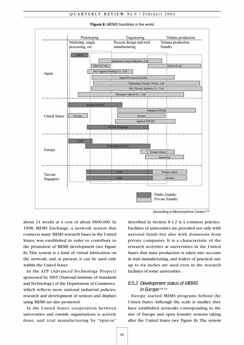
about 11 weeks at a cost of about ¥600,000. In
1998, MEMS Exchange, a network system that
connects many MEMS research bases in the United
States, was established in order to contribute to
the promotion of MEMS development (see Figure
8). This system is a kind of virtual fabrication on
the network, and, at present, it can be used only
within the United States.
In the ATP (Advanced Technology Project)
sponsored by NIST (National Institute of Standards
and Technology) of the Department of Commerce,
which reflects more national industrial policies,
research and development of sensors and displays
using MEMS are also promoted.
In the United States, cooperation between
universities and outside organizations is actively
done, and tr ial manufacturing by “Spin-in”
described in Section 8.4.2 is a common practice.
Facilities of universities are provided not only with
national funds but also with donations from
private companies. It is a characteristic of the
research activities at universities in the United
States that mass production is taken into account
in trial manufacturing, and wafers of practical size
up to six inches are used even in the research
facilities of some universities.
8.5.2 Development status of MEMSin Europe [18,19]
Europe started MEMS programs behind the
United States. Although the scale is smaller, they
have established networks corresponding to the
size of Europe and open foundry systems taking
after the United States (see Figure 8). The system
89
Q U A R T E R L Y R E V I E W N o . 6 / F e b r u a r y 2 0 0 3
Figure 8: MEMS foundries in the world
(According to Micromachine Center) [18]

formation was not spontaneous but purposefully
carried out with French LETI (Electronics and
Information Technology Laboratory), etc., at the
center, so that each country of the EU functions as
a member of the network. A representative MEMS
network is NEXUS, and the foundry exclusive for
MEMS is EUROPRACTICE; anyone can use these
facilities for tr ial manufacturing. In
EUROPRACTICE, users bear only one-third of the
prototyping cost, with one-third being subsidized
by local governments and the remaining one-third
subsidized by the EU.They accept orders from all
over the world, and some Japanese universities are
using the European foundries.
8.5.3 Development status of MEMS in Asia [18,20]
As in the cases of other fields, exchanges of
engineers between Western countries and Asia are
growing, contributing to the rise in the technical
level of Asian countries. Particularly in Taiwan and
Singapore, the governments are placing great
emphasis on this technology and the roles of the
public sector and the private sector are clearly
played. Public institutions take charge up to trial
manufacturing and private foundries take charge
of mass production. In Taiwan, common
laboratories are provided in ITRI (Industrial
Technology Research Institute of Taiwan), and
private foundries such as Walsin Lihwa Corp. are
implementating small-lot production of a wide
variety of products after taking over the results
achieved at ITRI (see Figure 8). Since MEMS
manufacturing processes are difficult to
standardize, it is unlikely that MEMS foundries will
grow as fast as the semiconductor foundries did in
the past. However, this field is being seriously
considered as a remedy to avoid the hollowing-out
in Taiwan, because their semiconductor foundries
may be jeopardized by the uprising of China.The
product field that is drawing the most attention is
RF MEMS described in Section 8.4.3.
8.6 Progress fromMEMS to NEMS
Many phenomena in nature are based on
reactions at the nano-level, and the science
intended to understand these phenomena is being
rapidly developed. In the research on MEMS as
well, there is a trend to mechanically or
electrically reproduce such phenomena, and
processing technologies at the nano-level are
being investigated. Such research activities have
been called NEMS (Nano Electro-Mechanical
Systems) since around 2000 [21]. For example,
miniature tubes provided on chips are considered
to be a highly efficient reactor, because chemical
reactions become more efficient with increasing
surface area. The concept that intends to
automatically reproduce on a chip chemical
experiments that are normally carried out in
chemical laboratories is called “Lab. on a Chip
(Laboratory on a chip).” The pioneer in this field
was the trial manufacturing of gas chromatograph
in 1975 as described in Section 8.2.2.
From the viewpoint of human size, it seems that
MEMS and NEMS have no great difference, but, as a
matter of fact, there is a great dif ference
comparable to that between an elephant and an
insect (see Figure 9).The miniaturization from
µm to nm by three orders of magnitude means
that the characteristics described in Section 8.3.3
are further enhanced. Higher resonance frequency,
higher mechanical response speed, lower power
consumption, lower noise, and higher thermal
response are expected.While many improvements
are expected, it must be taken into account that
the effect of surface conditions becomes greater
and static electricity has stronger effects. This
means that changes effected by environmental
conditions cannot be neglected.
The processing accuracy required for NEMS is
much severer than that required for MEMS. In the
present lithography technology, it is not easy to
form a line of 100 µm with a dimension error of
±1 µm; it is even less possible to obtain a
dimension error of ±1 nm for 100 nm.The level of
90
S C I E N C E & T E C H N O L O G Y T R E N D S
Figure 9: There is a great difference between micro andnano, comparable to that between an elephantand an insect.
processing accuracy for NEMS is comparable to
that for MEMS several decades ago [22].
Furthermore, even quantum fluctuations cannot
be neglected for a line width of 10 nm or less.
For these reasons, it is not conceivable that all
the research activities on MEMS should shift to
NEMS.The progress in miniaturization from micro
to nano is only one direction of the diversified
MEMS research activities. MEMS technology
essentially grows by diversification, and, in this
sense, it is different from semiconductor device
technology whose supreme target is
miniaturization, even though the same silicon
processing technology is involved. The evolution
of organisms was a history of the fearless struggle
for diversification, and it must be remembered that
in the history of organisms any attempt to unify
the form to the one considered to be the best
solution at the time resulted in failure. The latest
semiconductor processing technology is not
always required for medical devices such as
minimally invasive operation (a treatment that
does not cut the body very much, such as the one
in a blood vessel), biological devices such as DNA
chips, and chemical devices such as micro
reactors; more often than not, low costs are more
important than miniaturization. For example, it has
been shown that holes of about 100µm for micro
reactors could be processed without using silicon
processing technology [23].Therefore, the ability to
optimize the design process is required, including
judgment as to whether the use of silicon
processing technology is necessary.
8.7 For the promotion ofresearch on MEMS in Japan
8.7.1 Reflection on the peculiarity of thedevelopment of MEMS in Japan
Generally speaking, it is unlikely that the quality
or progress of research is affected by what the
technology is called. But in the particular case of
MEMS in Japan, it seems that the appellation gave
a significant effect on the course of research. Even
now, MEMS is often regarded as “micromachine” in
Japan.As is understood from this fact, research on
MEMS in Japan has been made mainly on
miniature machines typically represented by
micro robots. On the other hand, according to a
report on the investigation of nanotechnology in
the United States [24], micromachine (miniature
machine) and MEMS are classified into separate
fields that pursue different targets. It says that,
while Japan is ahead of the United States in
micromachine technology, it is far behind in MEMS
technology. We must admit that such situation in
the development of MEMS over the past 15 years
has been caused by the difference in
understanding — whether MEMS is considered as
“miniature machine” or as “miniature system.” In
Japan, micromachine technology has progressed
along with the development of robot technology
in which Japan is advanced. Although Japan has
made great progress in this field, commercial
products are still on the way to being developed.
In the past in Japan, microsensors were
considered to belong to another technical field or
as components used for micromachines, and they
have been developed mainly by private companies
as products for the parts supply business.
Ironically, sensor technology has grown into one
of the specialties of Japan. From now on,
micromachines should be regarded as
components for MEMS from a more
comprehensive viewpoint.
8.7.2 Development of human resources forsystem engineering
As described in Section 8.3.3, capable human
resources who have the ability to design a whole
system are required for the research on MEMS, but
it seems that Japan has a shortage of such qualified
personnel. Furthermore, it has been neglected in
technical education to train students in discussing
what to make in the manner as described in
Section 8.3.2. It has been pointed out that
Japanese industries excel at “how to make” but are
weak in “what to make” [13]. If one starts with
“how,” one cannot foster the capability to design
the whole system. One of the important roles of
Japanese universities and colleges in the future is
to nurture the engineers of “system engineering”
in its true sense.
8.7.3 Outsourcing of prototypesMEMS products are essentially manufactured by
large variety, small volume production [6].
Therefore, the mass-production-oriented concept
91
Q U A R T E R L Y R E V I E W N o . 6 / F e b r u a r y 2 0 0 3
that costs are reduced through volume production
even if prototypes are expensive must be
discarded, and commercialization factors must be
considered from the prototyping stage. However, it
is very difficult for organizations, even existing
private companies, to complete the cycle from
research and development through production to
marketing using their own facilities.
The Venture Business Laboratory of Tohoku
University and the Microsystem Technical Center
of Ritsumeikan University are examples of
common use facilities owned by universities in
Japan. Also, there are more than 10 private
foundries that accept orders for research and
small-scale prototyping [25]. At present, however,
most of the foundries cannot complete the desired
prototyping using a single process fab, and
sometimes it is impossible to complete the
prototyping through multiple process fabs due to
the difference in the size of silicon wafers. These
problems must be solved in the future by
appropriate means such as establishing networks.
So, now is the time to discuss how to effectively
utilize common facilities rather than constructing
new clean rooms for MEMS.
In the past, Japanese universities were unwilling
to carry out “fab-less” research, that is, without
having their own facilities to make the prototypes.
However, it is unrealistic for universities to have
on their own all the silicon processing facilities
required for providing prototypes. It is not always
economical even for private companies. If the
research on MEMS is understood as the “creation
of a new system,” it is more efficient for studying
“system engineering,” from the viewpoint of time
and economy, to eliminate the intermediate
prototyping stage. For education in MEMS, more
time should be spent on the verification and
analysis of finished products. To operate trial
manufacturing fabs that require diversity, the
researchers must prepare a considerable amount
of expense and labor as well as a certain number
of exclusive operators to keep them. It is
necessary to avoid increasing the number of
inefficient facilities neglecting these
disadvantages.
In March 2002, the Mechanical Social Systems
Foundation published a report compiled by the
Micromachine Center called the “Report on the
Investigation of the Foundry Network System
Concept for Micro/Nanotechnologies, Fiscal Year
2001” [18]. This report points out that there is a
mismatch between the expected initial market
size of MEMS and enormous investment required
for the processing facilities. It also advises that in
order to clear entry barriers, network systems
(FNS) should be established so that assets and
technologies, which are now being developed
randomly and separately, are integrated for the
best efficiency. In the concept of FNS, research
activities at universities and public institutions and
developments by private companies are integrated
into one system.When establishing a network, it is
important to make its size appropriate to the
market size and funding ability, and European
systems should be considered as models to follow.
8.7.4 Promotion of the venture aspect ofMEMS research
Regarding MEMS research activities, it is worth
noting that the orientation of research at
universities and that of the industry are in the
same direction, showing little discrepancy
between the two.This means that MEMS research
is an appropriate theme for the cooperative work
between industry and academia. It also should be
noted that MEMS is suitable for commercialization
by small-size companies and venture businesses.
Particularly, medical- and biology-related
technologies represent fields where venture
businesses are created most, with about 1,300
companies in the United States and more than 200
companies in Japan having been established up to
now [26]. Included among these venture businesses
are companies created by MEMS technology. For
example, Protein Wave was established in 2000
based on µ-TAS (µ-Total Analysis), a technology for
the crystallization of protein indispensable in the
research of genome (gene information) [27]. They
plan to commercialize silicon chips provided with
grooves or dents, in which protein solutions to be
crystallized are poured. They also intend to
develop new medicines by themselves. A road to
fund procurement has been opened in this field.
For example, a venture development association
has established [28] and a business plan
competitions have been held [29].
92
S C I E N C E & T E C H N O L O G Y T R E N D S

93
Q U A R T E R L Y R E V I E W N o . 6 / F e b r u a r y 2 0 0 3
8.7.5 Services available in JapanIf funds are sufficient, there is no restriction for
using universities and private foundries for the
research on MEMS. As a matter of fact, however,
universities without facilities and researchers who
intend to create venture businesses are suffering
from financial barriers. For these people, one
solution may be to utilize the facilities of other
universities and public institutions.
The following are examples of services available
to anyone. As for universities, the two mentioned
in Section 8.7.3 have the most experience. The
Institute of Electrical Engineers of Japan offers a
service called MICS (Micromachine Integrated
Chip Service), which provides micromachine
integrated chips [12]. In this service, multiple
prototypes are shared on one mask in order to
save the costs of trial manufacturing. But it must
be said that the available technologies are limited.
The Ministry of Education, Culture, Sports, Science
and Technology (MEXT) has established a
technical support system called the
Nanotechnology Support Project, and designated
14 organizations that anyone can use at no charge.
In this project, MEMS prototyping technology is
included [30]. Other than universities, efforts by
public institutions for shared research are not yet
active [18], however, one example of services
provided by local governments is the Technical
Support Center for Micro Device Development of
the Technology Research Institute of Osaka
Prefecture [31].
Some universities and private companies already
have experience in ordering prototypes of MEMS
from foundries in Europe and Taiwan, and
international cooperation has started in order to
cover the lack of domestic prototyping facilities.
However, if Japan loses the capability to develop
MEMS by itself, the hollowing-out of industry
would accelerate because the MEMS industry also
requires an integrated system from development
to manufacturing.
8.8 Conclusion
The research and development of MEMS is an
activity that creates new systems by integrating
microelectronics, nanoscience and other
technologies into micromachine and sensor
technologies that have been the specialty of Japan.
It requires system engineering education that
discusses “what” to make rather than “how” to do,
and it is very important to foster human resources
to handle the overall design including all of
conceptualization, design, and prototyping. Also,
for Japanese universities and private foundries for
MEMS, which are now being arranged to function
effectively for the vitalization of industry including
venture businesses, it is necessary to make organic
systematization taking after Europe.
Acknowledgements
I would like to express my sincere thanks to
Professor Masayoshi Esashi of Tohoku University,
Professor Shigeru Ando of Tokyo University,
Professor Kyoichi Ikeda of Tokyo University of
Agriculture and Technology, Professor Susumu
Sugiyama of Ritsumeikan University, Mr. Atsushi
Takano of Dainippon Printing Co., Ltd., Dr. Masaaki
Kimata of Mitsubishi Electric Corp., and Mr.
Takahiko Oasa of Sumitomo Metal Industries for
their precious advice relating to this report.
References
[1] Microelectromechanical Systems:Technology
and Applications, MRS BULLETIN,Vol. 26, No.
4, pp. 282-340 (2001.4).
[2] D. Bishop et al.,The Little Machines That Are
Making It Big, Physics Today,Vol. 54, No. 10, p.
38 (2001).
[3] M. Esashi, Introduction of three-dimensional
structures and different materials to the
differentiation technology of system LSI,
NIKKEI MICRODEVICES, September 2001, p.
125.
[4] K. Ikeda, Introduction to silicon
micromachine technology, Design Wave
Magazine, July, p. 101, September, p. 99,
November, p. 84 (2001).
[5] Silicon Light Machine web site, http://www.
siliconlight.com/htmlpgs/glvtechframes/.
[6] M. Esashi, New technical trends and
application perspective of MEMS,
ELECTRONIC PARTS AND MATERIALS, Vol.
41, No. 5, p. 18 (2002).
[7] Compiled by the Planning Section, National
Institute of Science and Technology Policy,

94
S C I E N C E & T E C H N O L O G Y T R E N D S
Science and Technology Agency,
Micromachine-Keyword for the newest
technology, p. 42 (1992).
[8] M. Waga, MEMS programs in the United
States, SEMI News,Vol. 17, No. 4, #12 (2001),
http://www.semi.org/.
[9] Texas Instruments, web site, http://www.ti.
com/corp/docs/company/history/.
[10] T. Hirano, Latest micromachine technology,
Journal of the Japan Society of Mechanical
Engineers,Vol. 105, No. 1004, p. 36 (2002.7).
[11] For example, Cybernet System, Ltd., MEMS
design and analysis software, MEMS ProTM,
http://www.cybernet.co.jp/memscap/.
[12] The Institute of Electrical Engineers of Japan,
Micromachine Integrated Chip Service,
http://www.e-mics.com/.
[13] M. Kimata et al., Micromachine expanding
from basic research to applications,Technical
Bulletin of Mitsubishi Electric Corp., Vol. 75,
No. 11, pp. 2-6, (pp. 698-702) (2001).
[14] IBM Japan, http://www.ibm.com/news/jp/
2002/06/06063.html.
[15] Power MEMS 2002 Program (http://www.
getinet.org/geti/).
[16] A. H. Epstein et al., Macro Power from Micro
Machinery, Science, Vol. 276, p. 1211
(1997.5).
[17] A. Pisano, MEMS Rotary Engine Power
System: Project Overview and Recent
Research Results.
[18] Micromachine Center, Report on the
investigation of the concept of foundry
networks for micro/nano manufacturing
technologies, (March 2002).
[19] M. Esashi, COMS2001 Report, http://www.
semi.org/.
[20] M.Waga, Rise of research and development of
MEMS in Asia, SEMI News, Vol. 18, No. 1, #17
(2002), http://www.semi.org/.
[21] H. G. Craighead, Nanoelectromechanical
Systems, Science, Vol. 290, No. 5496, p. 1532
(2000.11).
[22] T. Ono et al., From MEMS to NEMS, Applied
Physics,Vol. 71, No. 8, p. 982, (2002.8).
[23] H. Maeda, Micro space as a field for new
chemical reaction,AIST Today,Vol. 2, No. 8, p.
9 (2002.8).
[24] Mitsubishi Research Institute Inc.,
Investigation on the U. S. strategy for
promoting research and development of
nanotechnology, Achievement Report.
(2001.3).
[25] A. Takano, Current status of MEMS foundry
service, ELECTRONIC PARTS AND
MATERIALS,Vol. 41, No. 5, p. 22 (2002).
[26] H. Odagiri et al, Bio-venture companies in
Japan - significance and reality, National
Institute of Science and Technology Policy,
Ministry of Education, Culture, Sports,
Science and Technology, DISCUSSION PAPER,
No. 22 (2002.6), http://www.nistep.go.jp/.
[27] Protein Wave Corp., web site, http://www.
pro-wave.co.jp/.
[28] Japan Bio-venture Development Association,
http://www.jbda.jp/.
[29] Executive Committee for Japan
Biotechnology Business Competition,
http://www.mydome.or.jp/biocompe/.
[30] Nanotechnology Support Project, Ministry of
Education, Culture, Sports, Science and
Technology, http://www.mext.go.jp/b_menu
/houdou/14/02/020213g.htm. and http://
www.nanonet.go.jp
[31] Technical Support Center for Micro Device
Development, Technology Research Institute
of Osaka Prefecture, http://www.tri.pref.
osaka.jp/group/zairyou/microdl.htm.
(Original Japanese version: published in September 2002)