
Quantitative field mapping at the nanoscale by ...
169
HAL Id: tel-02974885 https://hal.archives-ouvertes.fr/tel-02974885 Submitted on 22 Oct 2020 HAL is a multi-disciplinary open access archive for the deposit and dissemination of sci- entific research documents, whether they are pub- lished or not. The documents may come from teaching and research institutions in France or abroad, or from public or private research centers. L’archive ouverte pluridisciplinaire HAL, est destinée au dépôt et à la diffusion de documents scientifiques de niveau recherche, publiés ou non, émanant des établissements d’enseignement et de recherche français ou étrangers, des laboratoires publics ou privés. Distributed under a Creative Commons Attribution - NonCommercial - NoDerivatives| 4.0 International License Quantitative field mapping at the nanoscale by transmission electron microscopy Christophe Gatel To cite this version: Christophe Gatel. Quantitative field mapping at the nanoscale by transmission electron microscopy. Materials Science [cond-mat.mtrl-sci]. Université Paul Sabatier Toulouse III, 2020. tel-02974885
Transcript of Quantitative field mapping at the nanoscale by ...

HAL Id: tel-02974885https://hal.archives-ouvertes.fr/tel-02974885
Submitted on 22 Oct 2020
HAL is a multi-disciplinary open accessarchive for the deposit and dissemination of sci-entific research documents, whether they are pub-lished or not. The documents may come fromteaching and research institutions in France orabroad, or from public or private research centers.
L’archive ouverte pluridisciplinaire HAL, estdestinée au dépôt et à la diffusion de documentsscientifiques de niveau recherche, publiés ou non,émanant des établissements d’enseignement et derecherche français ou étrangers, des laboratoirespublics ou privés.
Distributed under a Creative Commons Attribution - NonCommercial - NoDerivatives| 4.0International License
Quantitative field mapping at the nanoscale bytransmission electron microscopy
Christophe Gatel
To cite this version:Christophe Gatel. Quantitative field mapping at the nanoscale by transmission electron microscopy.Materials Science [cond-mat.mtrl-sci]. Université Paul Sabatier Toulouse III, 2020. �tel-02974885�

Titres et travaux pour l’obtention de
l’Habilitation à Diriger des Recherches
Quantitative field mapping at the nanoscale by
transmission electron microscopy
Christophe Gatel
Soutenue le 06 Février 2020 au CEMES devant le jury composé de :
• Mr Michael Lehmann Professeur
TU Berlin
Rapporteur
• Mme Alexandra Mougin Directrice de recherche CNRS
LPS Orsay
Rapporteure
• Mr. Jean-Luc Rouvière Chercheur
CEA-LEMMA Grenoble
Rapporteur
• Mr Vincent Cros Directeur de recherche
UMR CNRS-Thales, Palaiseau
Examinateur
• Mr Guillaume Saint-
Girons
Chargé de recherche
INL Lyon
Examinateur
• Mr Etienne Snoeck Directeur de recherche
CEMES Toulouse
Examinateur
• Mr. David. Guéry-
Odelin
Professeur
LCAR Toulouse
Prédisent du
jury
Ecole Doctorale Sciences de la Matière


TABLE OF CONTENTS
CURRICULUM VITAE ........................................................................................................................ 1
SUMMARY OF RESEARCH ACTIVITIES
Introduction ...................................................................................................................................... 7
I. Image formation in transmission electron microscopy ................................................. 9
I.1. Principle ................................................................................................................................... 9
I.2. Mathematical description .................................................................................................. 10
I.3. Electron beam phase shift ................................................................................................. 10
II. Structural investigations by HRTEM and correlation with material properties .............................................................................................................................................................. 14
II.1. Geometrical Phase Analysis (GPA) method............................................................... 14
II.1.a. Image decomposition ..................................................................................................... 15
II.1.b. Image reconstruction .................................................................................................... 15
II.1.c. Displacement field �� (�� )................................................................................................. 16
II.1.d. Deformation/Strain field ............................................................................................... 16
II.2. Quantum wells (QWs) in semiconducting materials ................................................ 17
II.2.a. Thin-foil effect on InAs QWs ....................................................................................... 17
II.2.b. Localized strain at InAs-AlSb interfaces .................................................................... 19
II.3. Magnetic materials ............................................................................................................ 22
II.3.a. Local investigation of the structural properties of ferrites and correlation with
magnetic properties .................................................................................................................. 24
II.3.a.1. Effect of antiphase boundaries (APBs) on magnetic properties of epitaxial Fe3O4
thin films ................................................................................................................................ 24
II.3.a.2. Ultrathin layers of NiFe2O4, MnFe2O4, and CoFe2O4 for spin-filter-based magnetic
tunnel junctions ...................................................................................................................... 25
II.3.a.3. Effect of the strain state on magnetic properties of epitaxial CoFe2O4 thin layers .. 26
II.3.b. Elaboration and magnetic transition of epitaxial FeRh thin films on MgO(001) ... 30
II.3.c. Magnetic particles elaborated by chemical routes ..................................................... 32
II.3.c.1. Air and water resistant Co nanorods ........................................................................ 32
II.3.c.2. Co-Fe dumbbells formation ..................................................................................... 35
II.4. Conclusion ........................................................................................................................... 39
III. Electric and magnetic field mapping using TEM ...................................................... 41
III.1. Introduction on magnetic mapping in TEM .............................................................. 45
III.2. The objective lens problem ........................................................................................... 45
III.3. Energy-loss Magnetic Chiral Dichroïsm .................................................................... 45
III.4. Lorentz Microscopy ........................................................................................................ 46
III.4.a. Principle ........................................................................................................................ 46
III.4.b. Results ........................................................................................................................... 48
III.5. Off-axis electron holography: principle and data treatment ................................. 50
III.5.a. Principle ........................................................................................................................ 50
III.5.b. Phase extraction and separation of the phase shift contributions........................... 52
III.5.c. Quantification from phase images .............................................................................. 55
III.5.d. A dedicated microscope ............................................................................................... 57
III.5.e. Off-line and live data treatments: qHolo & HoloLive! ............................................. 58
III.5.f. Double exposure ............................................................................................................ 60
III.6. Studies of magnetic configurations of nanosystems by EH .................................. 65
III.6.a. Micromagnetism .......................................................................................................... 65
III.6.b. Size effect in Fe nanoparticles .................................................................................... 67
III.6.c. The world of nanowires ............................................................................................... 72
III.6.c.1. Structure of a magnetic wall in a Ni nanowires ...................................................... 74
III.6.c.2. Structural and magnetic interplay in CoCu multilayered nanowires ...................... 76
III.6.c.3. Prospects for EH studies on nanowire .................................................................... 80
III.6.d. Inhomogeneous spatial distribution of magnetic transition in epitaxial layers ..... 82
III.6.d.1. Investigation of a FeRh thin film ............................................................................ 84
III.6.d.2. Magnetostructural transition as a function of the temperature of a MnAs layer .... 88
III.6.e. Operando investigation of a hard drive writing head ............................................... 92
III.6.f. Conclusion ..................................................................................................................... 96
III.7. Quantitative electrostatic mapping by EH ................................................................. 96
III.7.a. Elementary charge counting ....................................................................................... 96
III.7.b. Field emission of carbon nanocones ........................................................................... 99

RESEARCH PROJECT 103
P-I In situ/operando EH studies .......................................................................................... 104
P-I.1 Studies of electrical properties .................................................................................... 108
P-I.1.a . Operando biasing experiments on nanocapacitors: tools for studying dielectric and
ferroelectric properties .................................................................................................................... 108
P-I.1.a.1. A new geometry for sample preparation .............................................................. 109
P-I.1.a.2. Different nanocapacitors: from MOS to ferroelectric layers ............................... 109
P-I.1.a.3. Work program ...................................................................................................... 110
P-I.1.b Operando experiments on devices extracted from production lines ...................... 112
P-I.1.b.1. Microelectronics devices to be studied ................................................................ 112
P-I.1.b.2.Selection and electrical characterization of single devices ................................... 114
P-I.1.b.3. Device preparation for TEM observations ........................................................... 114
P-I.1.b.4. Device preparation for TEM observations ........................................................... 114
P-I.1.c Quantifying the Hall effect at the nanoscale ............................................................ 117
P-I.2 Studies of magnetic properties .................................................................................... 118
P-I.2.a Operando TEM studies for DWs manipulation under current .............................. 118
P-I.2.b Mapping the spin accumulation in spintronics devices using operando EH......... 119
P-I.2.c Spin wave imaging by EH .......................................................................................... 120
P-II Dynamic automation and complete simulation of electron trajectories in a
TEM ................................................................................................................................................. 123
P-II.1 Unlimited acquisition time by automated feedback control of a TEM ........... 124
P-II.1.a Phase detection limit in EH ...................................................................................... 125
P-II.1.b Correcting EH instabilities using dynamic automation ........................................ 127
P-II.1.b.1. Fringe control ..................................................................................................... 127
P-II.1.b.2. Specimen control ................................................................................................ 129
P-II.1.b.3. Removal of both fringe and specimen instabilities ............................................ 130
P-II.1.c Future of dynamic automation ................................................................................ 131
P-II.2 Simulation and visualization of electron trajectories in a TEM ....................... 132
P-II.2.a SIMION software ..................................................................................................... 133
P-II.2.b First results of a complete simulation of electron trajectories in a TEM ............ 134
P-II.2.c Future developments ................................................................................................ 137
Conclusion. .................................................................................................................................... 138
PUBLICATIONS ............................................................................................................................... 139
REFERENCES ................................................................................................................................. 148


1
Curriculum Vitae
CURRICULUM VITAE
PERSONAL INFORMATION
GATEL Christophe Married, 3 childs
07th June 1978, Rennes (France), French nationality Associate Professor
University of Toulouse - Paul Sabatier
CEMES-CNRS
EDUCATION
2001 - 2004 Ph.D. in Nanophysics, “Structure, magnetic and magnetotransport properties of an
hybrid system Ferrimagnetic oxide / Non-magnetic metal / Ferrimagnetic oxide"
CEMES-CNRS / Institut National des Sciences Appliquées (INSA-Toulouse).
PhD supervisor: Etienne Snoeck
2000 - 2001 Master’s degree in Nanophysics, INSA Toulouse (Rank: 1st)
1996 - 2001 Engineer’s degree in Physics
Institut National des Sciences Appliquées (INSA), Toulouse
POSITIONS
Since 2006 Permanent Associate Professor, Department of Physics at the University Paul Sabatier.
Research activities at the CEMES-CNRS laboratory.
2014-2019 IUF (Institut Universitaire de France) Junior Member
2004 - 2006 Post-doctoral position at CEA (Commissariat à l’Energie Atomique) Grenoble.
“Development of magnetic imaging for transmission electron microscopy”
Supervision: Pascale Bayle-Guillemaud
AWARDS
2017 Bronze Medal of CNRS
2014 IUF (Institut Universitaire de France) Junior Member
TEACHING ACTIVITIES
2006 – Permanent Associate Professor –Université Toulouse III-Paul Sabatier, France - ~200 h/year
2001 – 2004 Sessional Lecturer (Moniteur) – INSA Toulouse, France – 64h/year
In the past 10 years I have been teaching lectures (CM-Cours magistraux), practical tutorials (TD-Travaux
Dirigés) and practical labs (TP-Travaux pratiques) at bachelor (L-Licence) and master level (M). From 2012 to
2014, I obtained a 6 month-CNRS delegation fellow. This fellowship corresponds to a teaching reduction of
96h/year (on a normal teaching activity of 192h/year). From 2014 to 2019, I obtained a fellowship from the
Institut Universitaire de France (IUF) as junior member. My teaching activity has then been reduced to 64h/year
officially (in practice ~100h/year).

2
Curriculum Vitae
Since 2006, I have been teaching general physics courses as follow:
Bachelor:
• Mathematic tools (CM, TD)
• Optics (CM, TD, TP)
• Classical and quantum mechanics (CM, TD)
• Electromagnetism (CM, TD)
• Instrumentation (TP)
Master:
• Crystal growth and surface/interface physical properties (CM)
• Nanoscience and nanotechnologies (CM)
• Instrumentation and physical measurements (CM, TD, TP)
• Electron microscopy (CM, TP)
Having both a master’s degree and an engineer’s degree, I am also involved in selective bachelor’s degrees
which are preparing the students for engineer or long scientific studies. I give teaching lectures and practical
tutorials on physics (solid mechanics, electromagnetism, optics) at “Institut National Polytechnique (INP)” in
preparatory classes. In addition, I am examiner for the oral physics exam of the "Concours Communs
Polytechniques (CCP)" since 2008 (2 weeks each July) and for the physics exam of the "Ecole Nationale de
l’Aviation Civile (ENAC)" from 2009 to 2019.
I also participate in the annual reception of students from the Cazères secondary school: every year, about
twenty students and their physics and chemistry teacher (Pierre Baulès) visit the laboratory and carry out
practical work during the winter period, which they then return in the form of an oral presentation in May.
SUPERVISION OF GRADUATE STUDENTS AND POSTDOCTORAL FELLOWS
PhD Students: 3 completed / 4 on-going
2019-2022 Killian Gruel
Multiphysic modelisation of nanodevices
Co-supervised (50%) with M.J. Hÿtch, (CEMES)
1 publication in preparation
2019-2022 Maria Brodovoi
Development of in situ/operando characterization techniques in METs of semiconductor
devices & Correlation of physical and electrical characterization methods
Co-supervised (50%) with F. Lorut (STMicroelectroncs, Crolles)
2017-2020 Julien Dupuy
Development and optimization of electron interferometry experiments
Co-supervised (50%) with F. Houdellier, (CEMES)
1 co-signed publication, 2 in preparation
2017-2020 Marie Ingrid Andersen
In situ electron holography studies of magnetic nanosytems
Co-supervised (50%) with E; Snoeck (CEMES)
1 co-signed publication, 2 in preparation
2013-2016 David Reyes
Growth of multilayer nanowires by electrodeposition. Study of magnetic properties by
electron holography.
Co-supervised (50%) with B. Warot-Fonrose (CEMES)
5 co-signed publications

3
Curriculum Vitae
2012-2015 Marion Castiella
Elaboration, magnetic and structural studies of FeRh thin films.
Co-supervised (50%) with M.-J. Casanove (CEMES)
3 co-signed publications
2009 -2012 Elsa Javon
Development of dark filed electron holography: dynamical theory and propagation of the
geometrical phase
Co-supervised (50%) with M.J. Hÿtch (CEMES)
3 co-signed publications, 1 book chapter
Postdoctoral stages: 6 completed
2017 –2019 Raphaël Serra
Sample preparation of operando studies of nanodevices by EH
Co-supervised (50%) with M.J. Hÿtch (CEMES)
1 publication in preparation
2017 –2019 Luis-Alfredo-Rodriguez
Electron holography studies of magnetic nanosystems
Co-supervised (50%) with E. Snoeck (CEMES)
5 co-signed publication
2015 – 2016 Maxime Vallet
Study of epitaxial deformations at the interface of InAs/AlS quantum wells
Co-supervised (50%) with A. Ponchet (CEMES)
1 co-signed publication
2013-2015 Cécile Garcia-Marcellot
Local stuctural and magnetic studies of nanoparticles
Co-supervised (50%) with K. Soulentika (LPCNO)
2 co-signed publications
2012-2014 Julien Nicolai
Epitaxial strain studies at InAs/AlSb interfaces quantum wells
Co-supervised (50%) with A. Ponchet (CEMES)
5 co-signed publications
2008-2010 Jean-Pierre Ayoub
Elaboration, stuctural and magnetic studies of FeRh thin films
Co-supervised with M.-J. Casanove (CEMES)
1 co-signed publication
Master 2 students: 4 completed (3 pursued as PhD, 1 engineer)
February-July 2019: Killian Gruel
Multiphysic modelisation of nanocapacitors
February-July 2017: Julien Dupuy
Development and optimization of electron interferometry experiments
February-Sept. 2012: Polairk Kuong
Finite element calculations of Pt nanoparticles
February-June 2009: Elsa Javon
Study by electron holography of magnetic reversal of a magnetic junction

4
Curriculum Vitae
RESEARCH ACTIVITIES
Key words: Transmission Electron Microscopy, Electron Holography, In-situ experiments, High-resolution
microscopy, Data processing, Magnetic materials, Crystal growth, Strain measurement.
Few indicators are listed below. The details of these activities will be developed in the next sections.
101 PUBLICATIONS (87 articles and 14 proceedings) in peer-reviewed scientific journals (list at the end of
the manuscript)
>1700 citations, H-factor = 24 (ISI Web October 2019)
13 publications in first author.
Journals: Phys. Rev. Lett., Phys. Rev. B, Appl. Phys. Lett., J. of. App. Phys., Nature Communications,
Scientific Reports, Communication Physics, Ultramicroscopy, J. Magn. Magn. Mater., Surface science, J.
of Crystal Growth, Acta Materiala, Nano Letters, ACS Nano, Nano Research, Angw. Chem. Int. Ed, EPJB,
J. Phys. D.: Appl. Phys., Nanoscale, Nanotechnology,…
5 CHAPTERS in collective volume
• Magnetic Characterization Techniques for Nanomaterials, Edited by S.S.R. Kumar
Chapter Five: In Situ Lorentz Microscopy and Electron Holography Magnetization Studies of Ferromagnetic Focused
Electron Beam Induced Nanodeposits
C. Magen, L.-A. Rodriguez, L. Serrano-Ramon, C. Gatel, E. Snoeck and J.-M. Teresa
SpringerMaterials. DOI:10.1007/978-3-662-52780-1_9 (2017)
• Transmission Electron Microscopy in Micro-nanoelectronics, Edited by A. Claverie
Chapter Five: Magnetic Mapping Using Electron Holography
E. Snoeck and C. Gatel
ISTE, John Wiley and Sons, ISBN: 978-1-84821-367-8 (2013)
• Transmission Electron Microscopy in Micro-nanoelectronics, Edited by A. Claverie
Chapter Four: Dark-Field Electron Holography for Stain Mapping
M.J. Hÿtch, F. Houdellier, N. Cherkashin, S. Reboh, E. Javon, P. Benzo, C. Gatel, E. Snoeck and A. Claverie
ISTE, John Wiley and Sons, ISBN: 978-1-84821-367-8 (2013)
• Strain analysis in transmission electron microscopy: how far can we go?
Chapitre invité de l’ouvrage collectif “Mechanical Stress on the nanoscale”
A. Ponchet, C. Gatel, M.-J. Casanove and C. Roucau
Wiley-VCH Berlin (M. Hanbuecken, P. Müller, R. Wehrspohn, éditeurs) - Novembre 2011
ISBN-13: 978-3-527-41066-8
• Linear and Chiral Dichroism in the Electron Microscope. Edited by P. Schattschneider
Chapter Ten: Artefacts and Data Treatment in EMCD Spectra
K. Leifer, H. Lidbaum, J. Rusz, S. Rubino, C. Gatel and B. Warot-Fonrose
Pan Stanford Publishing Pte. Ltd., www.panstanford.com, ISBN: 978981426748
1 GRANTED PATENT
• Patent N° FR 1262755 "Nano objets magnétiques recouverts par une enveloppe métallique"
Inventeurs : A. Soulentika, S. Lentijo Mozo, M.T. Hungria-Hernandez, R. Tan and C. Gatel (December 2012)
3 SOFTWARE CONTRACTS
• CNRS Software and Patent License Agreement No. L16200. The contract for the commercialization of HoloLive!,
real-time hologram processing software, was signed between the CNRS and HREM Research Inc.
(www.hremresearch.com) on May 08, 2017 (authors: M.J. Hÿtch, C. Gatel).

5
Curriculum Vitae
• CNRS Software and Patent License Agreement No. L17054. The contract for the commercialization of the STEM
Moirés software for measuring deformation from moirés in scanning mode was concluded between the CNRS and
HREM Research Inc. (www.hremresearch.com) on May 08, 2017 (authors: M.J. Hÿtch, C. Gatel).
• CNRS Software and Patent License Agreement No. L10066. The contract for the commercialization of the
HoloDark software for the analysis of data from the CNRS patented process (No. 07 06711) was concluded between
the CNRS and HREM Research Inc. (www.hremresearch.com) on May 12, 2010 (authors: M.J. Hÿtch, C. Gatel).
DISSEMINATION OF FINDINGS
25 oral presentations in international conferences – 11 invitations
8 oral presentations in national conferences – 3 invitations
7 invited seminars
RESEARCH GRANT
Writing of national and European grants (ERC Consolidator, ranked B). In coordinator, 2 were successful.
2014-2019: Institut Universitaire de France, 75 k€
2017-2021: ANR IODA (In Operando electron microscopy for Device Analysis), Coordinator, 460 k€
INSTITUTIONAL RESPONSIBILITIES
Since 2016 Leader of the I3EM group (In situ, Interferometry and Instrumentation for Electron
Microscopy) consisting of 6 permanent staff. It is 1 of 7 groups of the CEMES laboratory.
Since 2016 Member of the direction committee of the CEMES laboratory.
2018-2022 Leader of the associated international laboratory LIA M²OZART (Materials and
Microscopy Consortium Zaragoza Toulouse) with INA/ICMA of Zaragoza (Spain) and
LPCNO-INSA of Toulouse.
2016-2020 Member of the Scientific Council, of University Paul Sabatier (Toulouse III)
2013-2018 Member of the scientific college « Physique SDU » (sections 28-29-30-34-37). This
committee is in charge of constituting the boards for the hiring of lecturers and professors
2010-2013 Member of the scientific committee of the « Journées Surface/Interface » (JSI)
COMMISSIONS OF TRUST
Since 2006 Reviewer for ~6 papers per year for different journals (Nature Communications, Nano Letters,
Ultramicroscopy, Phys. Rev. B., Appl. Phys. Lett.,…)
2018 Examiner for Habilitation thesis (Dr. Martien Den Hertog), University Grenoble Alpes,
Institut Louis Néel, France.
2017 Selection Committee (member) for permanent position of associate professor, University of
Lille, France
2014-2019 Expertise Committee of Léon Brillouin laboratory. Selection of proposals concerning
magnetic materials for beam line time.
2014 Examiner for PhD thesis (Dr. Luis-Alfredo Rodriguez), University of Zaragoza Institut of
Nanoscience of Aragon, Spain.

6
Curriculum Vitae
ORGANISATION OF SCIENTIFIC MEETINGS
2019 Louis Neel conference, Organising committee, ~200 participants, Toulouse, France.
2019 Nanomagnetism workshop in the framework of associated international laboratory M²OZART
with ~20 participants. February 2019 at Zaragoza, Spain.
2018 Annual meeting of the associated international laboratory M²OZART with ~30
participants. March 2018 at Banyuls, France.
2013 Quantitative Electron Microscopy (QEM2013) with 100 participants. From 12 to 24 may
2013 at Saint-Aygulf, France.
2009 Quantitative Electron Microscopy (QEM2009) with 100 participants. May 2009 at Saint-
Aygulf, France.
MAJOR COLLABORATIONS
At the present time and not to mention the cooperation with CEMES researchers:
• L.-M. Lacroix, T. Blon, . Soulantika, LPCNO-INSA, Toulouse (France)
• A. Masseboeuf, O Fruchart, Spintec, Grenoble (France). ANR IODA and ANR MILF
• M. Den Hertog, Institut Néel, Grenoble (France)
• F. Lorut, L. Clément, N. Bicais, STMicroelectronics, Crolles (France). ANR IODA
• A. Lubk, D. Wolf, Institute for Solid State Research, Dresden (Germany)
• C. Magen, J.-M. De Teresa, R. Arena, Institut of Nanoscience of Aragon” (INA) – University of
Zaragoza- CESIC, Zaragoza (Spain). LIA TALEM1&2 LIA M²OZART, ESTEEM2 & 3
• M. Vasquez, A. Asenjo, C. Bran, Instituto de Ciencia de Materiales de Madrid – CSIC, Madrid (Spain)
• L-A. Rodriguez, Department of Physics, Universidad del Valle, Cali (Columbia)
• ESTEEM 1, ESTEEM 2 and ESTEEM 3: European project with transnational access and joint research
activities. Cooperation with many European laboratories involved in advanced TEM studies: LPS-Orsay
(France), EMAT-Antwerp (Belgium), ERC-Jülich (Germany), Oxford (UK),…
7
Research activities - Introduction
SUMMARY OF RESEARCH ACTIVITIES
Introduction
The extraordinary progress of Nanosciences and Nanotechnologies in recent years results from the unique
properties that appear in materials and devices as their physical dimensions are reduced. At some point, the
properties of nano-objects can no longer be deduced from the macroscopic behavior by a simple scaling law.
Either the influence of surfaces and interfaces become preeminent or the object exhibits dimensions below the
characteristic length scales of physical properties under consideration. For example, superplasticity has been
observed in nanocrystalline material when the grain structure modifies the normal action of dislocations, the
defects which mediate plasticity1,2, and magnetic nanoparticles become superparamagnetic when their
dimensions become smaller than the typical width of domain walls.3,4 Many investigations have thus revealed
the exceptional magnetic, mechanical, electronic, optical and catalytic properties of nanoparticles5, nanowires
and thin films. Some of these unique properties already have found industrial applications in a broad range of
fields such as medicine, chemistry, optics, microelectronics or data storage. For instance, the current digital
revolution results from the important size reduction of components coupled with the increased speed of
transistors but it also benefits from the extraordinary progress in optoelectronics and imaging sensors (Nobel
Prize 2000, 2009, and 2014).6–12 The data storage is continuously facing breakthrough with the discovery of
new phenomena such as the giant magnetoresistance effect used in hard disks readings heads (Nobel Prize 2007)
and joint developments around spintronics.13–17 Many potential applications exist such as the use of magnetic
nanoparticles for the local treatment of the tumors by hyperthermia18–20, the astonishing promises of carbon
nanotubes and graphene (Nobel Prize 2010)21,22, and the recent developments based on topological phase
transitions and topological phases of matter (Nobel Prize 2016).23–25
One of the most important challenges in previously mentioned discoveries is to get access and to control
phenomena at the nanoscale with an appropriately sensitive tool. This ability to target new physical phenomenon
as well as manipulating newfound objects is crucial for fundamental physics leading to application
breakthroughs. Transmission Electron Microscopy (TEM) is the appropriate tool: its broad sensitivity ranges
from atomic structure to atomic-scale analysis of valence states and chemistry. TEM can also determine the
electrostatic, magnetic and deformation fields at the nanometer scale using scanning methods as differential
phase contrast or interferometric methods as electron holography. The ability of TEM to probe individual nano-
object instead of assemblies of nano-objects provides the unmeasurable potential discoveries. Many examples
prove the potentiality of TEM to observe new phenomena such as skyrmions which are a major building block
of the promising spintronics26–29, or to address new concepts. For instance, the observation of Electrons with
Orbital Angular Momentum waves (i.e. phase singularity)30 have recently put out to date a new future of
information transmission integration31 or non-contact manipulation32,33. Nanometre-scale surface plasmon
resonances34 also opened the door to optical antennas35 and their application in optoelectronics and energy. In
situ TEM experiments offer the possibility to observe phenomena that occur for very high stimulus values.
Indeed, working at nanometre distances on nanoscale objects with confined fields allows electric fields higher

8
Research activities - Introduction
than GV.m-1 to be easily reached, current densities greater than 1010 A.m-2 or magnetic field gradients on
nanometric widths. As an example, a voltage of 10 V applied on a distance of 10 nm creates an electric field of
10 GV.m-1. When scaling this distance up to 1 cm the equivalent voltage to be applied would be of 107 V, which
is unrealistic (except in a lightning storm). Physical phenomena associated with such high stimuli could then be
investigated at the local scale.
My research activities and my project presented in this manuscript are parts of the nanoscience field. In this
exciting field, my goal has always been to explore the physical properties of individual nanosystems through
TEM experiments, from nanoparticle to device. After graduating as an engineer in physics and nanophysics in
2001 from the National Institute of Applied Sciences (INSA) in Toulouse, I started a Ph.D. (Supervisor: E.
Snoeck) at the Centre for Materials Elaboration and Structural Studies (CEMES). I had to elaborate an epitaxial
multilayer system consisting of ferrimagnetic oxides (Fe3O4, CoFe2O4) and non-magnetic metals (Ag, Au, Pt)
by sputtering. I determined the optimal growth conditions for the structural and magnetic properties in order to
measure a magneto-resistance effect by specular reflections of electrons at the non-magnetic
metal/ferromagnetic interfaces. I performed structural studies by conventional and high-resolution transmission
electron microscopy. Then I reinforced my skills in electron microscopy and magnetic materials during my
postdoctoral work at the CEA Grenoble (2004-2006) where I had to develop and implement optical alignments
and data extraction for magnetic imaging electron microscopy (Lorentz microscopy) under the supervision of
P. Bayle.
In September 2006, I was hired as a lecturer at the University Paul Sabatier. My research activities were then
focused on the study of strain in quantum wells of semiconducting materials and the relationships between
structural and magnetic properties of materials in various forms (thin films, nanoparticles...) using high-
resolution transmission electron microscopy. I refocused my work ten years ago on the development of novel
techniques, especially off-axis electron holography (EH), and their use for measuring the physical properties of
nanomaterials. In particular, electron holography is an exciting and very powerful interferometric method for
quantitative electromagnetic field mapping. However, I quickly realized that this technique suffered from
different drawbacks and many bottlenecks had to be solved before fully exploiting its huge possibilities. I thus
focused my efforts on the development of software for automatic and live data treatment as well as on model
experiments to study in situ electromagnetic phenomena on nano-objects when they are stimulated by an
external stimulus. The pursuit of these developments and the possibilities they offer for operando studies of
nanodevices as well as the feedback control and simulations of the microscope are the guidelines of my project.
This manuscript follows and summarizes this research path. In the first part, I briefly present the principle of
the formation of an image in TEM. The second part concerns the structural investigations I conducted using
high-resolution microscopy and their correlation with the material properties. The third part is focused on my
works on the electric and magnetic field mapping of various systems at the nanoscale. Backgrounds on magnetic
imaging in TEM and off-axis EH are given before presenting the developments on EH and different studies I
performed. The last part will conclude this report with the project I plan to conduct.
9
I. Image formation in transmission electron microscopy
I. Image formation in transmission electron microscopy
I start this report by giving some details about the image formation in a transmission electron microscope
which will be useful in the next sections concerning high-resolution TEM for structural studies of nanosystems,
and electron holography developments and experiments which concerns the main part of my activity and the
project.
I.1. Principle
The overall process of the image formation in TEM can be summarized in six steps, which follow the electron
wave trajectory:
1. Creation and acceleration of an electron beam from an electron source.
2. Illumination of the specimen with the (coherent) electron beam.
3. Scattering of the electron wave by the specimen transparent to electrons
4. Formation of a diffraction pattern in the back focal plane of the objective lens.
5. Formation of an image of the specimen in the image plane of the objective lens.
6. Projection of the image (or the diffraction pattern) on the detector plane.
In the first step, electrons are generated either by thermionic emission of a filament (tungsten or LaB6) heated
at high temperatures, or by field emission using a Cold Field Emission Gun (C-FEG) where electrons are
extracted from an extremely sharp tungsten tip (W(310)) at room temperature or by the combination of both
methods in the so-called Schottky Field Emission Gun (S-FEG). The C-FEG and S-FEG guns are highly
coherent and bright electrons sources, essential for EH, while thermionic sources provide more intense but less
coherent beams. In the second step, electron waves are accelerated (typically up to 60 kV to 300 kV) and the
illumination system (a set of two or three condenser lenses) allows defining the beam (probe size, convergence
angle, electron dose) that irradiates the top surface of the specimen. The electron wave then interacts with the
sample through various scattering process, either elastic or inelastic, followed by the formation of a diffraction
pattern in the back focal plane. Finally, the formation of the image is possible in the image plane.36
It is important to note that the specimen has to be thinned for achieving electron transparency. The thickness
for electron transparency depends on the material, the energy of electron beam and the methods to be used. For
a 300kV microscope, this thickness is for instance between a few nanometres and about 200nm.
A schematic representation of the image formation in TEM following this simple idea is displayed in Fig.
I.1.

10
I. Image formation in transmission electron microscopy
Fig. I.1. Left: signals generated by the electron beam-specimen interaction. Right: basic schematic
representation of the image formation by the objective lens in a TEM. Red lines represent the optical path
followed by the electrons during the image formation process.
The electron-specimen interaction modifies the incident electron wave through elastic and inelastic scattering
phenomena. A summary of the signals generated by the electron-specimen interaction is also illustrated in the
inset of Fig. I.1. In inelastic scattering processes, the electrons loose a small amount of energy that is transferred
to the specimen producing the emission of a wide range of secondary signals (x-rays, visible light, secondary
electrons, phonons and plasmons excitations), also damaging the specimen.37 These secondary signals are used
to perform analytical TEM experiments such as x-ray energy-dispersive spectroscopy (XEDS), electron energy-
loss spectroscopy (EELS) or cathodoluminescence. On the other hand, in elastic processes, the electrons are
scattered without losing energy. In crystalline materials, the elastic scattering gives rise to Bragg diffraction
related to the constructive interference of the scattered electron waves in a periodic crystal. Thus, Bragg
scattering results in a series of diffracted beams scattered at angles dependent on the lattice periodicities of the
crystal structure. The elastically scattered electron beams are the ones used to form images in TEM techniques
such as diffraction-contrast TEM38 and phase-contrast High-Resolution TEM (HRTEM).37
I.2. Mathematical description
The mathematical description of the image formation process in a TEM is described as follows. According
to quantum mechanics, the scattering of a high energy electron plane wave interacting with a crystalline
specimen can be described by the relativistic time-independent Schrödinger equation, also known as Dirac
equation.39 Considering the weak phase object approximation (electrons are scattered elastically by a thin

11
I. Image formation in transmission electron microscopy
specimen and absorption effects are neglected), its solution at the exit surface of the specimen is a transmitted
wave function in the direct space 𝑟 = (𝑥, 𝑦, 𝑧) called object electron wave:
ψobj(r ) = A(r )eiϕ(r ) Eq. I.1
where 𝐴(𝒓) is the amplitude of the exit wave function and 𝜙(𝒓) is a phase shift induced by the potential with
which the electrons interact when passing through the sample. Next, the object electron wave propagates and
the objective lens creates a diffraction pattern in its back focal plane and an image of the specimen in its image
plane. According to diffraction theory, electrons scattered by the same lattice planes converge in a common
point in the back focal plane, creating a representation of the specimen in the reciprocal space (i.e. a diffraction
pattern). From a mathematical point of view, such a diffraction pattern is the Fourier transform (ℱ) of the object
electron wave:
𝛹obj(k ) = ℱ[ψobj(r )] Eq. I.2
where �� is the reciprocal vector. The Fourier transform Ψ𝑜𝑏𝑗(�� ) is defined as:
𝛹obj(k ) = ∫ψobj(r ) e(2πik ∙r )dr3 Eq. I.3
In the image formation process, the object electron wave is modified by the aberrations of the objective lens
(mainly defocus, astigmatism and spherical aberration). These optical artefacts can be introduced by means of
a transfer function, 𝑇(�� ), multiplying the object electron wave in reciprocal space, Ψ𝑜𝑏𝑗(�� ). Thus, the
diffraction wave function, Ψ𝑑𝑖𝑓𝑓(�� ), in the back focal plane becomes the following function:40,41
𝛹diff(k ) = 𝛹obj(k )T(k ) Eq. I.4
In general, the transfer function can be expressed as:
T(k ) = B(k )eiχ(k )e−ig(k ) Eq. I.5
where 𝐵(�� ) is a pre-exponential function associated with the use of a cut-off aperture and magnification effects,
𝑔(�� ) is a damping function which accounts for all the microscope instabilities (lens current, acceleration
voltage, etc.) and the incoherence of the electron probe, and 𝜒(�� ) is the phase contrast function, which contains
the phase shift introduced by the lens aberrations (defocus, astigmatism, coma, spherical aberrations, etc.).
Neglecting high order aberration factors, 𝜒(�� ) can be expressed as:
χ(k ) =2π
λ[CS
4λ4k4 +
∆z
2λ2k2 −
CA
2(ky
2 − kx2)λ2] Eq. I.6
where 𝐶𝑆 is the spherical aberration coefficient, 𝐶𝐴 is the axial astigmatism coefficient, 𝜆 is the electron
wavelength and ∆𝑧 is the defocus. Finally, the objective lens forms an image of the object in the image plane
Ψ𝑖𝑚𝑔(𝑟 ) in real space, which corresponds to an inverse Fourier transform of Ψ𝑑𝑖𝑓𝑓(�� ).
𝛹img(r ) = ℱ−1[𝛹diff(k )] = ℱ−1[𝛹obj(k )T(k )] Eq. I.7

12
I. Image formation in transmission electron microscopy
Afterwards, intermediate and projector lenses magnify and transfer the image of the object to a conjugated plane
where the detector (e.g. fluorescent screen, charge-coupled-device CCD camera, CMOS camera, direct electron
detector,…) records the image as an intensity map of the image electron wave. The image intensity is expressed
as the squared modulus of Ψ𝑖𝑚𝑔(𝑟 ):
I(r ) = |𝛹img(r )|2= 𝛹img(r ) ∙ (𝛹img(r ))
∗ Eq. I.8
In an ideal microscope free of optical defects where images are recorded at zero defocus (Gaussian focus),
without aberrations, aperture cut-off or incoherence, 𝑇(�� ) = 1 and the intensity is:
I(r ) = |𝛹img(r )|2= |A(r )|2 Eq. I.9
In such an ideal case, 𝐼(𝑟 ) only records the amplitude of the object electron wave, losing the information
contained in the phase shift, 𝜙(�� ). Furthermore, in weak phase objects, the amplitude is homogeneous, resulting
in an image without any contrast at all. As we will see in the next section, the study of magnetic materials by
TEM experiments requires to be able to record the phase shift of the object electron wave.
I.3. Electron beam phase shift
The phase of an electron wave is modified when interacting with an object and with an electromagnetic field
around it. From quantum mechanics, we know that the electron function that describes the behaviour of
relativistic electrons in an electromagnetic field can be deduced from the Dirac equation, where the electron
spin would be neglected:
1
2me(−iℏ𝛻 + eA)2𝛹(x, y, z) = e[U∗ + γV]𝛹(x, y, z) Eq. I.10
where 𝐴 and 𝑉 are the magnetic and electric potential respectively, 𝑒 is the electron charge, 𝑚𝑒 is the rest mass
of the electron, 𝛾 is the relativistic Lorentz factor [𝛾 = 1 + 𝑒𝑈 𝑚𝑒𝑐2⁄ ] and 𝑈∗ is the relativistic corrected
accelerating potential (𝑈∗ = (𝑈 2⁄ )(1 + 𝛾), where 𝑈 is the non-relativistic accelerating potential). The solution
of this equation corresponds to the object electron wave of the equation 𝜓𝑜𝑏𝑗(𝑟 ) = 𝐴(𝑟 )𝑒𝑖𝜙(𝑟 ) (Eq. I.1), where
its phase shift is modified due to the Aharonov-Bohm effect:42,43
ϕ(x, y) =πγ
λU∗ ∫𝑉(r )dz −e
ℏ∫Az(r )dz Eq. I.11
with 𝜆 = ℏ (2𝑒𝑚𝑒𝑈∗)1 2⁄⁄ the electron relativistic wavelength, and 𝐴𝒛 the component of the magnetic vector
potential 𝐴 along the beam direction. The Eq. I.11 can also be expressed as:44
ϕ(x, y) = CE ∫V(r )dz −e
ℏ∬B⊥(r )drdz Eq. I.12
where 𝑉 corresponds to the mean inner potential and 𝐵⊥ is the magnetic component of the induction along the
direction perpendicular to the two-dimensional position in the object plane and 𝐶𝐸 = (𝜋𝛾 𝜆𝑈∗⁄ ) is an interaction
constant that only depends on the energy of the incident electron beam. 𝐶𝐸 takes values of 7.29 × 10⁶,
6.53 × 10⁶ and 5.39 × 10⁶ rad. V−1.m−1 at accelerating voltages of 200kV, 300kV and 1MV, respectively.

13
I. Image formation in transmission electron microscopy
Eq. I.11 and I.12 underline that, when the electrons propagate through a specimen, the phase shift contains
information about the electrostatic potential (mean inner potential related to the composition, and density and/or
presence of an excess of electric charges) and the magnetic vector potential (magnetic induction) if the sample
present magnetic properties. Therefore, it becomes possible to map the electric and the magnetic properties by
TEM if the phase shift resulting from the interaction of the object electron wave with the electromagnetic field
can be analysed. It is important to note at this point that only in-plane components of the magnetic induction,
i.e. components perpendicular to the beam direction, participate in the magnetic phase shift. In other words, the
parallel component to the electron beam cannot be detected in TEM. In addition, the total phase shift
corresponds to a projection and an integration of the different potentials along the electron path. As a
consequence, a constant thickness of the sample is often required to facilitate the data interpretation.
A common strategy to extract information from the phase shift of the electron wave is to tune the transfer
function of the microscope in order to modulate the electron wave and obtain an image whose intensity is related
to the phase shift. This strategy is used in HRTEM to resolve atomic columns, and it is known as phase-contrast
imaging. In advanced TEM with 𝐶𝑆-aberration corrector, the transfer function can be modulated through the
phase contrast function by a slight variation of the focal distance ∆𝑧. The image contrast in HRTEM can be
analysed using different methods of data treatment and gives information on the variation of the periodicity of
atomic planes, allowing a measurement of the atomic displacement and thus the deformation and strain as a
function a reference area. I applied the Geometrical Phase Analysis (GPA) method45–47 on HRTEM images for
studying structural properties of many systems and explaining how the local strain can modify the expected
properties. This research axis is detailed in the next section.
Extracting the electron beam phase shift is needed for quantitative magnetic or electric mapping (Eq I.11
and I.12). However, in normal condition, only the spatial distribution of the intensity (the square of the
amplitude) of the electron wave is recorded by the detector and consequently, the phase shift term is lost.
Electron holography (EH) records the interference between a part of the beam that has interacted with an object
and the surrounding electromagnetic fields, called “object wave”, with another part of the beam that has not
interacted with any field, called the “reference wave”. The intensity of the image, e.g. hologram, which results
from the superposition of the two waves, preserves the phase shift term which will be extracted using data
treatment. The principle, as well as the use and developments I conducted in EH, is detailed in section I.

14
II. Structural investigations by HRTEM and correlation with material properties
II. Structural investigations by HRTEM and correlation with material properties
TEM is one of the most used methods for investigating structural and chemical properties of nanosystems at
the nanoscale. Its flexibility allows studying 2D materials or bulk materials, of various chemical composition.
But its main advantage is also its main drawback: if it is possible to reveal and probe a particular defect by a
very local analysis, it is very difficult to obtain a statistical analysis of these defects. One thing to keep in mind
during a TEM experiment: is the area observed representative of the sample?
However, local analyzes of structural and chemical properties by TEM remain very relevant, in particular
when they become quantitative and allow to be correlated with macroscopic measurements of properties. For
instance, the elastic strain is a key parameter of epitaxial heterostructures. It results from the elastic
accommodation of the lattice misfit between two materials, for instance the substrate and the deposited layer.
The resulting state of strain has strong implications in growth modes and in nanostructure properties. In this
context, the internal strain is one essential parameter to characterize epitaxial layers and to investigate the related
properties.
In the following, I give some examples demonstrating the efficiency of quantitatively analyzing images
obtained in high resolution microcopy for a deeper investigation of local structural properties of the nanosystem.
After introducing the basic of the Geometrical Phase Analysis (GPA) method, I present some works performed
on the strain state analysis of semiconducting quantum wells. Then I will detail different studies using HRTEM
on various magnetic nanomaterials, from epitaxial thin films to complex nanoparticles. In each of these
examples, I will highlight how the determination of the local properties correlated with results obtained from
various methods for measuring others properties allowed for an enhanced understanding of the nanosystem.
II.1. Geometrical Phase Analysis (GPA) method
The GPA method aims at quantitatively determining the displacement and strain fields of atomic columns in
a sample from high-resolution images. As explained previously, the image contrast obtained in high-resolution
electron microscopy is not a simple function of the position of atoms but the combination of parameters defined
by the imaging conditions (voltage, defocusing of the objective lens, spherical aberrations…) with parameters
related to the sample (thickness, orientation ...). When atomic columns appear in the form of Gaussian intensity
peaks, one can locate them and evaluate their displacements by comparison with a reference area. However, in
cases where atomic columns do not respect this intensity distribution, the method cannot be applied. The GPA
method avoids the search for atomic peaks and minimizes the importance of imaging conditions.45–47 Using a
Fourier transform, the high-resolution image of a crystal is considered as a sum of sinusoidal fringes. As a
consequence, the displacement (phase) of these fringes correspond to the phase of the coefficients in the Fourier
transform of the image and provides information on displacement of fringes, i.e. atomic planes.

15
II. Structural investigations by HRTEM and correlation with material properties
II.1.a. Image decomposition
The intensity of the high-resolution image at the position 𝑟 is decomposed in a sum of Fourier components.
For an image with a perfect periodicity of the crystal lattice:
𝐼(𝑟 ) = ∑ 𝐻𝑔𝑒2𝜋𝑖�� .𝑟 𝑔 Eq. II.1
where 𝑔 corresponds to a Bragg reflection, 𝐻𝑔 the corresponding Fourier component. The summation is
performed in the reciprocal space where only the 𝑔 vectors related to the periodicities present in the image have
a large amplitude. The deviations of a real crystal from the perfect crystal are introduced by making 𝐻𝑔
dependent on the position:
I(r ) = ∑ Hg(r )e2πig .r
g Eq. II.2
Complex images 𝐻𝑔(𝑟 ) can be decomposed in terms of amplitude and phase as 𝐻𝑔(𝑟 ) = 𝐴𝑔(𝑟 )𝑒𝑖𝑃𝑔(𝑟 ). By
selecting only a single spot in the Fourier transform of the image and calculating the inverse Fourier transform,
the intensity in the image is written:
Bg(r ) = 2Ag(r )cos (2πg . r + Pg(r )) Eq. II.3
From this equation, phase and amplitude terms can be separated for creating two distinct images. The
amplitude image gives the contrast of a set of fringes at a particular position in the image. Amplitude variations
are related to changes in sample thickness, composition, imaging conditions, or loss of periodicity (in the
vicinity of a defect, for example). The phase image represents the deviation of the position of the fringes at the
ideal position. For a non-periodic image, a periodicity defect can be considered in real space or in reciprocal
space:
• In the real space, it represents the displacement of the fringe position. We thus obtain 𝐵𝑔(𝑟 ) =
2𝐴𝑔(𝑟 )𝑐𝑜𝑠(2𝜋𝑔 . 𝑟 − 2𝜋𝑔 . �� (𝑟 )) corresponding to the displacement of the cosine maximum for a value
�� (𝑟 ). The relationship between the phase and displacement is 𝑃𝑔(𝑟 ) = −2𝜋𝑔 . �� (𝑟 ). The component of
the displacement field �� (𝑟 ) can therefore be determined from the phase image.
• In the reciprocal space, a defect is equivalent to a variation of the periodicity of the fringes. In that case,
𝐵𝑔(𝑟 ) = 2𝐴𝑔(𝑟 )𝑐𝑜𝑠(2𝜋𝑔 . 𝑟 + 2𝜋∆𝑔 . 𝑟 ) and 𝑃𝑔(𝑟 ) = −2𝜋∆𝑔 . 𝑟 .
The position of the fringes of maximum intensity does not necessarily correspond to the position of the
atomic planes. However, the periodicities of the fringes in the image are related to the periodicities of the atomic
planes in the studied crystal.
II.1.b. Image reconstruction
The Fourier transform of the image, analogue of the crystal diffraction pattern (without considering the
intensities of the spots which depend on the structural factors), consists of spots related to the periodicities of
the crystal lattice and is called diffractogram. A spot, corresponding to a single spatial periodicity, is selected

16
II. Structural investigations by HRTEM and correlation with material properties
using a mask and the image related to this periodicity is reconstructed in amplitude and phase. The phase image
2𝜋(𝑔 + ∆𝑔 ). 𝑟 + 𝑃𝑔(𝑟 ) had to be treated for removing the 2𝜋∆𝑔 . 𝑟 term which represents the difference between
the real value of 𝑔 and the value measured during the selection of the spot. A reference area is then chosen for
which 𝑔 is fixed at the real value. The difference between the value of the selected periodicity and the value of
the periodicity in the reference area is finally subtracted from the whole image.
II.1.c. Displacement field �� (�� )
�� (𝑟 ) can be extracted from a high-resolution image by selecting two different spots 𝑔1 and 𝑔2 on the
diffractogram, and by calculating the corresponding phase images :
𝑃𝑔1(𝑟 ) = −2𝜋𝑔1 . �� (𝑟 ) = −2𝜋 (𝑔1𝑥. 𝑢𝑥(𝑟 ) + 𝑔1𝑦. 𝑢𝑦(𝑟 ))
Pg2(r ) = −2πg2 . u (r ) = −2π(g2x. ux(r ) + g2y. uy(r )) Eq. II.4
The reference area has to be the same for both images to avoid variation in periodicity. The expressions of
the displacements in x and y directions in the image plane are deduced from Eq. II.4:
𝑢𝑥(𝑟 ) = −1
2𝜋
𝑃𝑔1(𝑟 ).𝑔2𝑦−𝑃𝑔2(𝑟 ).𝑔1𝑦
𝑔1𝑥.𝑔2𝑦−𝑔1𝑦.𝑔2𝑥
uy(r ) = −1
2π
Pg2(r ).g1x−Pg1(r ).g2x
g1x.g2y−g1y.g2x Eq. II.5
𝑔1 and 𝑔2 has not to be collinear. If not, phase images are similar and the denominator is equal to 0.
II.1.d. Deformation/Strain field
Calculation of the derivatives of �� (𝑟 ) gives access to the local deformation with respect to the reference
zone:
𝜕𝑢𝑥(𝑟 )
𝜕𝑥= 휀𝑥𝑥(𝑟 )
𝜕𝑢𝑦(𝑟 )
𝜕𝑦= 휀𝑦𝑦(𝑟 )
∂uy(r )
∂x= εyx(r )
∂ux(r )
∂y= εxy(r ) Eq. II.6
To avoid an accumulation of errors, the components of the deformation tensor are calculated directly from
the phase images and not from the displacement images. Partial derivatives of phase images are written:
𝜕𝑃𝑔1(𝑟 )
𝜕𝑥= −2𝜋𝑔1 .
𝜕�� (𝑟 )
𝜕𝑥= −2𝜋 (𝑔1𝑥.
𝜕𝑢𝑥(𝑟 )
𝜕𝑥+ 𝑔1𝑦.
𝜕𝑢𝑦(𝑟 )
𝜕𝑥)
𝜕𝑃𝑔1(𝑟 )
𝜕𝑦= −2𝜋𝑔1 .
𝜕�� (𝑟 )
𝜕𝑦= −2𝜋 (𝑔1𝑥.
𝜕𝑢𝑥(𝑟 )
𝜕𝑦+ 𝑔1𝑦.
𝜕𝑢𝑦(𝑟 )
𝜕𝑦)
𝜕𝑃𝑔2(𝑟 )
𝜕𝑥= −2𝜋𝑔2 .
𝜕�� (𝑟 )
𝜕𝑥= −2𝜋 (𝑔2𝑥 .
𝜕𝑢𝑥(𝑟 )
𝜕𝑥+ 𝑔2𝑦.
𝜕𝑢𝑦(𝑟 )
𝜕𝑥)
∂Pg2(r )
∂y= −2πg2 .
∂u (r )
∂y= −2π(g2x.
∂ux(r )
∂y+ g2y.
∂uy(r )
∂y) Eq. II.7

17
II. Structural investigations by HRTEM and correlation with material properties
We deduce the expressions of the partial derivatives of the displacements:
𝜕𝑢𝑥(𝑟 )
𝜕𝑥= 휀𝑥𝑥(𝑟 ) = −
1
2𝜋
𝜕𝑃𝑔1(�� )
𝜕𝑥.𝑔2𝑦−
𝜕𝑃𝑔2(�� )
𝜕𝑥.𝑔1𝑦
𝑔1𝑥.𝑔2𝑦−𝑔1𝑦.𝑔2𝑥
𝜕𝑢𝑥(𝑟 )
𝜕𝑦= 휀𝑥𝑦(𝑟 ) = −
1
2𝜋
𝜕𝑃𝑔1(�� )
𝜕𝑦.𝑔2𝑦−
𝜕𝑃𝑔2(�� )
𝜕𝑦.𝑔1𝑦
𝑔1𝑥.𝑔2𝑦−𝑔1𝑦.𝑔2𝑥
𝜕𝑢𝑦(𝑟 )
𝜕𝑦= 휀𝑦𝑦(𝑟 ) = −
1
2𝜋
𝜕𝑃𝑔2(�� )
𝜕𝑦.𝑔1𝑥−
𝜕𝑃𝑔1(�� )
𝜕𝑦.𝑔2𝑥
𝑔1𝑥.𝑔2𝑦−𝑔1𝑦.𝑔2𝑥
∂uy(r )
∂x= εyx(r ) = −
1
2π
∂Pg2(r )
∂x.g1x−
∂Pg1(r )
∂x.g2x
g1x.g2y−g1y.g2x Eq. II.8
The method does not give direct access to the deformation of the crystal with respect to its massive state. In
the case where the reference material is not the same as the one on which the deformation is measured, the
deformation of the studied material becomes 𝜕𝑢𝑥
𝜕𝑥= 휀𝑥𝑥 +
∆𝑎
𝑎 where ∆𝑎 represents the parametric mismatch
between the reference area and the study area, and a is the parameter of the reference material.
The knowledge of the strain tensor for the studied material allows calculating the strain components from the
deformation ones.
II.2. Quantum wells (QWs) in semiconducting materials
In my early time as lecturer and in collaboration with A. Ponchet (CEMES), I studied the structural properties
using HRTEM and GPA method of III–V semiconducting quantum wells (QW) grown on GaAs or InP
substrates. These systems present strategic importance for optoelectronics devices and are characterized by a
mismatch of lattice parameters between the substrate and the QWs. To ensure optical properties like light
emission, the lattice mismatch must be accommodated through elastic deformation of the QWs (dislocations
being non-radiative recombination centres). Therefore, the resulting state of strain has strong implications on
the growth modes and on the device properties. The internal strain is thus one essential parameter to characterize
epitaxial layers and understand optical properties. Because of the nanometric scale of QWs, HR(S)TEM is one
of the experimental approaches particularly suitable for measuring the actual state of strain or stress. Compared
to other methods of epitaxial strain determination, HR(S)TEM has the advantage of providing a direct and very
local image of the strained system with a high spatial resolution, giving also information on layer thicknesses,
interfacial morphology and extended defects.
II.2.a. Thin-foil effect on InAs QWs
For all TEM based methods, the strain determination is affected by the thinning needed to make the sample
transparent to the electron beam. Previous studies showed that the key parameter is the ratio between the sample
thickness along the thinned direction and the superlattice period.48,49 If the thickness is much larger than the
period, the stress remains biaxial; as the thickness decreases, the symmetry of stress tensor and strain tensor is

18
II. Structural investigations by HRTEM and correlation with material properties
reduced and one tends to uniaxial stress along the direction of the plane perpendicular to the observation.
Experimental analysis of strained InAlAs superlattices50 has evidenced inhomogeneous strain fields and a
reduction of the average strain in accordance to this theoretical approach. Experimental values of smaller strain
than expected have also been observed in single layers.51 As also theoretically expected, a stress transfer from
the layers to the buffers has been seen in HR(S)TEM experiments and extended very far in the substrate.52
Estimating the thin foil effect, i.e. the actual modification of strain due to thinning for electron transparency,
remains nevertheless a delicate issue for HR(S)TEM observations due to various artifacts, as for instance those
caused by the bending of the lattice planes. But the main source of incertitude is the lack of data on the surface
relaxation. The hypothesis made on the sample thickness, too thin to be accurately measured, contributes to the
experimental incertitude. Then, theoretical and numerical analyses are based on the hypothesis that the sample
has a finite size in the direction of thinning, but is infinite along the direction perpendicular, so that the strain in
this direction is fixed by the nominal misfit. That was one of the aims of the first study I conducted on a III-V
semiconducting system.
This system was composed of nanometric InAs QWs grown by molecular beam epitaxy (MBE) using a
residual flux of Sb on Ga0.47In0.53As/InP(001) substrate [A22]. Despite a high epitaxial strain due to a nominal
lattice mismatch of 3.2%, at least 15 monolayers (MLs) of
InAs (equivalent thickness equal to 4.5 nm) can be grown
at 460°C without relaxation while the critical thickness of
the 2D–3D transition is usually around a few MLs. In
collaboration with A. Ponchet (CEMES), I performed
HRTEM experiments and applied GPA method to
investigate the elastic strain of these QWs: a lattice
distortion was detected within the buffers below and above
the InAs layers (Fig. II.1). I showed that the buffers are
under tensile stress, which is the signature of a significant
transfer of stress from the layer to the buffers due to surface
relaxation effect in these experimental observation
conditions.
For a quantitative analysis of the thin foil effect,
numerical simulations were performed using three-
dimensional (3D) Finite Element Modeling (FEM).
Compared to two-dimensional (2D) FEM and to the
analytical approach, 3D FEM does not impose that the
sample is infinite in the directions of the image plane. 3D
FEM has the advantage of allowing the possible occurrence
of foil bending and large displacements, making possible
the modeling of any thin foil geometry and crystallographic
direction. In the range of the strained layer thickness
Fig. II.1. (a) HRTEM image of 15 MLs of InAs
in [110] zone axis; (b) GPA map of the
displacements parallel to the growth axis
(spatial resolution of 2 atomic planes). The
arrow indicates the growth direction.

19
II. Structural investigations by HRTEM and correlation with material properties
considered here (3–5 nm), 3D FEM showed that the reduction of the measured strain due to thin foil effect is
unavoidable in HR(S)TEM experiment, and reaches about 10–25% of the initial value. In addition, experimental
displacements in the buffer layers may not be reproduced completely by a classical FEM model in which the
foil relaxes only in the direction of observation. The buffer distortion calculated by FEM is very sensitive to the
boundary conditions adopted in the model to simulate surface relaxation effects (Fig. II.2). It is exalted by an
additional surface relaxation along the direction of the observation. The displacements in the buffers are
impacted by this effect even at several hundred nm from the additional free surface. This is due to an enhanced
transfer of stress from layer to buffers. Considering surface relaxation effects, the uncertainty in the strain
determination due to surface relaxation (10%) is larger than the one due to the image analysis itself. The
experimental level of elastic strain in the [001] direction is thus found to be in excellent agreement with the one
calculated by elasticity for a pure InAs layer (3.5%), demonstrating the existence of high epitaxial stress in these
thick layers. Fitting experimental data by a model integrating surface relaxation is thus essential to retrieve the
strain before thinning from HR(S)TEM images and to estimate the precision of the strain measurement.
II.2.b. Localized strain at InAs-AlSb interfaces
Like the previous example, almost all studies on QWs have been focused on determining the strain inside
nanometric layers. However, the strain variation at interfaces themselves is more complex: strong strain
gradients can occur at interfaces because of chemical exchanges over several atomic planes. In addition, the
juxtaposition of two materials without common atomic species requires different chemical bonds at interfaces
compared to the two materials. In some cases, these interfaces can undergo a larger distortion than the layers
themselves. This situation is not the most frequent in the epitaxy of III-V compounds, where the simultaneous
change of group III and group V elements is often avoided, but it is not fictitious. Indeed, the alternation of
Fig. II.2. Displacements Uz parallel to the growth axis
calculated across a 15 MLs layer of InAs embedded
inGa0.47In0.53As buffers (Curves artificially shifted in the Uz-axis
for a better readability). The introduced mismatch is 3.2% and
the foil thickness tx is 13 nm (tx/h = 3). Dashed line: relaxation
effect only in the direction parallel to the interfaces. Full lines:
free surface effect in the y direction, at a distance ty from the
analyzed zone. Dotted lines: relaxed boundary conditions at the
bottom (free surface 80 nm below the strained layer).
GaInAs GaInAs InAs

20
II. Structural investigations by HRTEM and correlation with material properties
wells and barriers without common atoms enhance physical properties for some systems, particularly for
antimonide-arsenide systems like AlSb/InAs and GaSb/InAs. The AlSb/InAs system alternates a wide bandgap
material and a small gap material and it presents a very large conduction band discontinuity of 2.1 eV, beneficial
for the fabrication of short wavelength Quantum Cascade Lasers (QCLs).53 The lattice mismatch between the
two binaries InAs and AlSb is moderate (1.3%) but the formation of specific chemical bonds at interfaces such
as Al-As or In-Sb may result in large and very-localized strains. Indeed, the lattice parameters of AlAs (0.566
nm) and InSb (0.6479nm), as bulk materials, differ significantly from that of the substrate InAs (0.6058 nm)
and their lattice misfit with InAs is -6.6% and +6.9%, respectively [Swaminathan]. Al-As or In-Sb type
interfaces can thus present very large local distortions, which can affect the device properties through a loss of
structural quality and a modification of the band structure.54,55
Although this issue has been identified for a long time, very few studies have been done on the strain induced
by this lack of common atoms. In collaboration with A. Ponchet and J. Nicolai (postdoc), I thus investigated
more deeply the elastic strain induced by the interfaces themselves and the nature of the interfacial bonds in this
system at the scale of the interface [A45, A61, A68]. The out-of-plane strain has been extracted using GPA
method applied on HRTEM images obtained from a Cs-corrected Tecnai F20 microscope (CEMES), and
correlated with the chemical composition of the interfaces analyzed by HAADF-STEM (CS-probe corrected FEI
Titan at INA-Zaragoza) where the intensity contrasts are directly related to the atomic number of elements
(intensity varies as Zn, with n close to 1.7). However, translate strain data into chemical data in a quaternary
system does not lead to a unique solution. Only semi-quantitative information can be deduced from the GPA
method like AlAs-rich (tensile stress) or InSb-rich (compressive stress) interfaces. Similarly, several chemical
compositions can account for one HAADF intensity profile and only qualitative chemical information can also
be obtained. But the combination of these two techniques allowed a more precise description of the interface
composition (Fig. II.3).
Fig. II.3. (a) ε⊥ strain map from GPA of an
[110] zone axis HRTEM image, (b) ε⊥ strain
profile averaged on the whole width of the
image (30 nm), (c) HAADF-STEM micrograph
obtained on the same area, (d) Intensity profile
from HAADF image plotted along the growth
direction.

21
II. Structural investigations by HRTEM and correlation with material properties
As molecular beam epitaxy (MBE) is an out-of-equilibrium process, the interface formation is a sequential
process, which depends on the succession of microscopic events that occur at the surface. It is well known that
due to this feature, direct and reverse interfaces are generally not equivalent and as a consequence the formation
of one of the possible interfacial configurations could be favored. We thus choose to investigate a multilayer
with very simple interfacial sequences where we tried to force the two extreme cases, i.e. either Al-As or In-Sb
type interface. In practice, a very short sequence of either AlAs or InSb was introduced; the duration of the
deposit corresponded to 0.7 monolayer. In parallel, examining the growth sequence and using only a limited
number of hypotheses, we determined the possible chemical composition of the interfaces. These assumptions
are: (i) the elements of group V can desorb while those of group III cannot, (ii) exchanges are possible between
In and Al, due to In segregation versus Al, and (iii) between Sb and As leading to better incorporation of As
than Sb. Moreover, we assume (iv) that the more the bonding is strong, the more it is favored.
TEM image analysis showed that spontaneously, without any special flux conditions, Al-As bonds were
favored on both AlSb on InAs interfaces and InAs on AlSb interfaces. We assumed that the Al-As type interface
is favored due to its high thermal stability and bond energy. Then, the intentional insertion of either an AlAs or
InSb sequence gave a clear insight into the mechanisms favoring the formation of these interfaces. Indeed, the
intentional addition of one AlAs layer at the first interface (AlSb on InAs) should reinforce the natural tendency
towards Al-As type interface and increase the tensile stress (negative out of plane strain), which is actually
observed. At the second interface (InAs on AlSb), the addition of one AlAs layer should lead to the formation
of a very high tensile interface, but the experimental analysis suggests a more moderate tensile stress, in
agreement with the possible mixing of elements V suggested by the sequence analysis. On the contrary, the
addition of one InSb monolayer at the first interface is clearly useless under these growth conditions, leading to
a wide interface, with moderate tensile stress. At the second interface the addition of one InSb monolayer
produces strong compressive stress, as expected; however, an Al0.5In0.5Sb rich interface is formed rather than
InSb due to the unstable character of In-Sb bond. The use of these rules leads to the determination of the
chemical composition of the interfaces in a very good agreement with the experimental results. We also showed
that the interface composition could be tuned using an appropriate growth sequence.
We used this strong localized strain at InAs/AlSb interfaces to study the ability of GPA of determining the
actual level of strain in that case. Indeed, the application of GPA to interfaces with abrupt and huge variations
of both atomic composition and bond length requires some caution. Due to the technical limitations of the
method which relies on a filtering in the Fourier space of the image (spatial resolution, choice of the reference
zone…) and to the averaging effects in the direction of observation, the strain value at the scale of an interface
cannot be measured as precisely as in thicker layers. In particular, the actual strain is probably larger than the
measured one. During the postdoc of M. Vallet we have thus performed a strain analysis on atomic-resolved Z-
contrast images acquired by HAADF-STEM thanks to an improved process of image acquisition which removes
the detrimental effects of image drift [A68]. Experimental strain profiles were compared to those obtained from
simulated images, with a focus on the effect of convolution due to the mask used in the GPA treatment (Fig.
II.4).

22
II. Structural investigations by HRTEM and correlation with material properties
The combination of strain and intensity profiles analysis confirmed the high content of AlAs bonds at
interfaces spontaneously assembled in InAs/AlSb multilayers for QCLs. With the best spatial resolution allowed
by the numerical mask used in GPA, a negative strain of about 6% was measured at interfaces which is of the
same order of magnitude in an image generated from a model structure with perfect AlAs interfaces. Intensity
profiles performed on the same images confirmed that changes of chemical composition are the source of high
strain fields at interfaces. The results show that spontaneously assembled interfaces are not perfect but extend
over 2 or 3 monolayers.
To conclude on this part, my work on the strain states of QWs using HRTEM was also conducted through
various collaborations which led to the following articles: [A23, A46, A56].
II.3. Magnetic materials
This research axis on the correlation between structural and magnetic properties of nanosystems started
during my Ph.D. thesis. The aim was to analyze the spin dependence of electron reflection at interfaces. For
that, I had to experimentally measure the current-in-plane giant magnetoresistance (CIP-GMR) effect which is
only produced by the spin-dependent interfacial reflection by elaborating an appropriate system. In this
framework, I had first to explore the experimental conditions for growing by sputtering a monocrystalline
heterostructure composed of epitaxial layers. More precisely, two ferromagnetic semiconducting or insulating
Fig. II.4. Out-of-plane strain ε⊥ maps from a high resolution image with spatial
resolutions of 1 nm (a), 0.7nm (b), and 0.45 nm (c). The diffractograms with the different
mask sizes are shown in insets. Corresponding profiles of strain along the growth
direction (integrated over the width of the image in the [110] direction) are displayed
in (d), (e), and (f), respectively.

23
II. Structural investigations by HRTEM and correlation with material properties
layers, i.e. CoFe2O4 and Fe3O4 with different coercivity fields Hc1 and Hc2 respectively, separated by a
nonmagnetic metallic Au or Pt layer. In such a system, the conducting electrons were confined in the bi-
dimensional epitaxial metallic layer and were reflected at the interfaces. An antiparallel configuration of
ferrimagnetic layer magnetization was obtained for magnetic fields ranging between Hc1 and Hc2 while a parallel
alignment of them is achieved for fields larger than the higher coercive field.
Once the optimal growth conditions have been determined, the interfacial flatness and the high structural
quality of the multilayers have been evidenced by TEM. The electrical measurements confirmed that the
electrical conduction occurred within the metallic layer. A CIP-GMR effect was observed at low temperature
which has been ascribed only to the spin-dependent reflection at the metal/ferrimagnetic insulator interfaces.
The increase of the GMR in the CoFe2O4 /Fe3O4 /Au/Fe3O4 symmetrical system reached 5% at 10 K and the
first observations of the decrease of the GMR with the Au/ferrimagnetic interface roughness increase
highlighted a CIP-GMR effect due to the spin dependence of electron reflection at the interfaces with a large
contribution of specular reflections [A6].
The elaboration of this system required to conduct several studies in parallel. The first one was focused on
the epitaxial growth of Ag, Au and Pt on Fe3O4(001) and (111) layers epitaxially grown on MgO(001) and
Al2O3(0001) substrates. The aim was to obtain a very thin but continuous and monocrystalline metallic layer
with the lowest possible roughness [A2, A3, A7, A10]. I thus obtained results leading to physical interpretation
about their growth modes and structural properties as a function of the growth temperature, the deposited
thickness and the growth direction. A second study was dedicated to the control of exchange bias between Fe3O4
and the antiferromagnetic oxide NiO as a function of their structural properties [A5]. The aim was to obtain
Fe3O4 layers with different coercive field and shifted hysteresis loop for having both antiparallel and parallel
magnetic configurations of the whole CIP-GMR heterostructure. The epitaxial growth of Fe3O4 and NiO layers
has been achieved on the two Al2O3(0001) and MgO(001) substrates. Detailed structural analyses allowed me
to characterize the epitaxial structure and the quality of the interface for both [001] and [111] growth directions
while magnetic measurements have permitted the study of the influence of two drastically different types of
Fe3O4/NiO interfaces on the exchange coupling. This study is a perfect example of the interpretation of the
measured magnetic properties through a local investigation of structural properties by TEM.
I conducted other studies in different magnetic materials focusing my work on the correlation of the structural
properties obtained by quantitative analysis from HRTEM images with the measured magnetic properties. These
materials could be oxides or metals, in epitaxial thin films or nanoparticles. In the following, I give a summary
of the related studies trying to highlight the context and the results.

24
II. Structural investigations by HRTEM and correlation with material properties
II.3.a. Local investigation of the structural properties of ferrites and correlation with
magnetic properties
II.3.a.1. Effect of antiphase boundaries (APBs) on magnetic properties of epitaxial Fe3O4 thin
films
The use of ferrite materials, i.e. Fe3O4 et CoFe2O4, into the heterostructure elaborated for studying the spin-
dependent reflections of electrons allowed me to deeply investigate by TEM the link between their structural
and magnetic properties. In particular concerning Fe3O4 for which many studies have been conducted since the
2000’s. Fe3O4, so-called magnetite, presents a cubic (inverse) spinel structure as all ferrite materials (NiFe2O4,
CoFe2O4, MnFe2O4,…). Its chemical formula, often written as [Fe3+]A[Fe2+]BO4 indicates that the tetrahedral
sites denoted as A are occupied by ferric ions (Fe3+) while octahedral sites denoted as B contain an equal number
of ferric and ferrous ions (Fe2+). The tetrahedral and octahedral sites form two magnetic sublattices with the
spin moments on the A sub-lattice antiparallel to those on the B sub-lattice, at the origin of its ferrimagnetic
property. Contrary to all others ferrite materials which are insulating, magnetite belongs to the half-metallic
materials which present a considerable interest for spin electronics applications as they are fully spin polarized,
i.e. conductors for one spin direction and insulators for the other. Indeed, the band structure calculations have
predicted a half-metallic behavior56–58 at 300 K and above while its Curie temperature reaches 860 K. In addition,
magnetite presents a band structure transition around 120K (Verwey transition) highlighted by a change of its
electrical and magnetic properties due to a modification of the crystallographic structure (monoclinic to spinel
structure). If the explanation of the Verwey transition is nowadays still under debates, its appearance is the sign
of high quality films.
However, the amplitude of the giant magnetoresistance59 or tunnel magnetoresistance60–67 of devices
including Fe3O4 is much lower than expected from the predicted half-metallic character. An explanation for this
discrepancy has been found in the significant differences between the magnetic properties of Fe3O4 thin films
and those of bulk samples.68–70 One of the puzzling features of the magnetic behavior of Fe3O4 thin films is the
lack of saturation even under large applied fields up to 70 kOe. This has been qualitatively ascribed to the
presence of the antiphase boundaries (APBs) which are structural defects present in various compounds
including bimetallic alloys (Cu3Au, FexRh1-x, FexAl1-x, …) and oxides. The influence of APBs on magnetic
properties comes from the existence of specific geometries of the Fe-O-Fe arrangements not present in perfect
Fe3O4 crystalline structure. Although APBs have also been observed in bulk spinels71, they are mostly associated
with Fe3O4 thin films and more specifically with the coalescence of islands exhibiting different cation
sublattices. APBs have been observed in Fe3O4 thin films epitaxially grown onto a great variety of substrates,
e.g. MgO, Al2O3, Pt, and even the original spinel MgAl2O4. The APB network was first thought to be set during
the very first stages of growth.72
Thanks to a collaboration with a research team of CEA Saclay (J.-B. Moussy, A.M. Bataille and
collaborators), we performed a large study on Fe3O4 layers elaborated by sputtering (CEMES) or by MBE under
monoatomic oxygen (CEA Saclay) with different growth directions. We quantitatively analyzed the APB
network by TEM as a function of the growth conditions (temperature, thickness) and the nature of the substrate
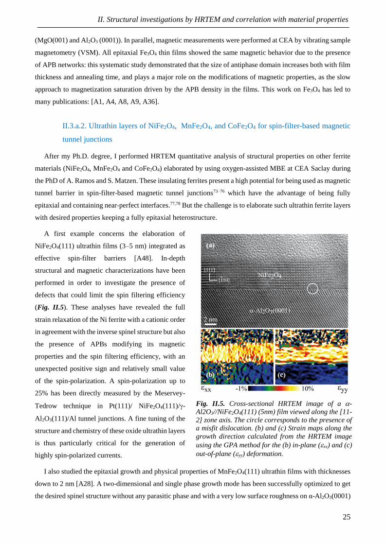
25
II. Structural investigations by HRTEM and correlation with material properties
(MgO(001) and Al2O3 (0001)). In parallel, magnetic measurements were performed at CEA by vibrating sample
magnetometry (VSM). All epitaxial Fe3O4 thin films showed the same magnetic behavior due to the presence
of APB networks: this systematic study demonstrated that the size of antiphase domain increases both with film
thickness and annealing time, and plays a major role on the modifications of magnetic properties, as the slow
approach to magnetization saturation driven by the APB density in the films. This work on Fe3O4 has led to
many publications: [A1, A4, A8, A9, A36].
II.3.a.2. Ultrathin layers of NiFe2O4, MnFe2O4, and CoFe2O4 for spin-filter-based magnetic
tunnel junctions
After my Ph.D. degree, I performed HRTEM quantitative analysis of structural properties on other ferrite
materials (NiFe2O4, MnFe2O4 and CoFe2O4) elaborated by using oxygen-assisted MBE at CEA Saclay during
the PhD of A. Ramos and S. Matzen. These insulating ferrites present a high potential for being used as magnetic
tunnel barrier in spin-filter-based magnetic tunnel junctions73–76 which have the advantage of being fully
epitaxial and containing near-perfect interfaces.77,78 But the challenge is to elaborate such ultrathin ferrite layers
with desired properties keeping a fully epitaxial heterostructure.
A first example concerns the elaboration of
NiFe2O4(111) ultrathin films (3–5 nm) integrated as
effective spin-filter barriers [A48]. In-depth
structural and magnetic characterizations have been
performed in order to investigate the presence of
defects that could limit the spin filtering efficiency
(Fig. II.5). These analyses have revealed the full
strain relaxation of the Ni ferrite with a cationic order
in agreement with the inverse spinel structure but also
the presence of APBs modifying its magnetic
properties and the spin filtering efficiency, with an
unexpected positive sign and relatively small value
of the spin-polarization. A spin-polarization up to
25% has been directly measured by the Meservey-
Tedrow technique in Pt(111)/ NiFe2O4(111)/-
Al2O3(111)/Al tunnel junctions. A fine tuning of the
structure and chemistry of these oxide ultrathin layers
is thus particularly critical for the generation of
highly spin-polarized currents.
I also studied the epitaxial growth and physical properties of MnFe2O4(111) ultrathin films with thicknesses
down to 2 nm [A28]. A two-dimensional and single phase growth mode has been successfully optimized to get
the desired spinel structure without any parasitic phase and with a very low surface roughness on α-Al2O3(0001)
Fig. II.5. Cross-sectional HRTEM image of a -
Al2O3//NiFe2O4(111) (5nm) film viewed along the [11-
2] zone axis. The circle corresponds to the presence of
a misfit dislocation. (b) and (c) Strain maps along the
growth direction calculated from the HRTEM image
using the GPA method for the (b) in-plane (xx) and (c)
out-of-plane (yy) deformation.

26
II. Structural investigations by HRTEM and correlation with material properties
single crystals or Pt(111) buffer layers. The HRTEM measurements have clearly revealed the excellent
structural quality of the manganese ferrite ultrathin films with sharp interfaces and low roughness. The electrical
and magnetic properties shown that MnFe2O4(111) layers keep adequate properties (highly insulating behavior
without pin holes on large surfaces) to be used as tunnel barriers at room temperature. This study proved the
high potential of MnFe2O4 to be used as a magnetic tunnel barrier for spin filtering applications at room
temperature.
I performed several studies on epitaxial CoFe2O4 thin
layers in collaboration with J.-B. Moussy and A. Ramos
(CEA Saclay). The insulating Co ferrite is especially
interesting as it presents a very high coercive field due to
the highest magnetostriction coefficient reported79,80,
offering the capability of mastering the magnetization with
strain. In a first step, I studied its structural properties by
HTREM when depositing on Pt(111) buffer layers or α-
Al2O3(0001) substrate [A13, P9]. The high quality of the
fully epitaxial growth and interfaces (Fig. II.6) have
demonstrated room temperature spin filtering in
Pt(111)/CoFe2O4(111)/-Al2O3(111)/Co(0001) magnetic
tunnel junctions where CoFe2O4 was the magnetic tunnel
barrier: tunnel magnetoresistance (TMR) values of −18%
and −3% were observed at 2 and 290 K, respectively.
Furthermore, the experimental TMR ratio increased with increasing bias voltage, reproducing the theoretically
predicted behavior for a model spin filter system. I have also conducted structural studies of spin filter systems
containing CoFe2O4(111) barriers and Co(111) or Fe3O4(111) top electrodes [A11],. The structural and chemical
characteristics of these CoFe2O4(111)-based epitaxial heterostructures with near-perfect interfaces have proven
to be crucial in the interpretation of their magnetic properties. The magnetic study unveiled important
differences in the magnetization behavior of the oxide/metal and oxide/oxide systems produced by the distinct
exchange interactions at their interfaces. In particular, unique phenomena were found in the case of the
CoFe2O4/Fe3O4 bilayers due to the interactions found exclusively in ferrimagnetic oxides. This exceptional
system revealed an exchange spring magnet effect that most dramatically affects the second layer to switch,
resulting in a system that is blocked in the antiparallel state with respect to the applied magnetic field.
II.3.a.3. Effect of the strain state on magnetic properties of epitaxial CoFe2O4 thin layers
The previous results showed that magnetic properties of spinel ferrites, especially CoFe2O4, are often
modified when these oxides are deposited as thin films (decrease of magnetization, Curie temperature or
coercive field). In all previous examples, CoFe2O4 was elaborated along the [111] growth direction, with a large
misfit (>6%) compared to the substrates or the buffer layer, and presented a high density of APBs. In order to
Fig. II.6. HRTEM image of a CoFe2O4 (5
nm)/-Al2O3 (1.5 nm)/Co(10 nm) trilayer
deposited directly on a sapphire substrate.

27
II. Structural investigations by HRTEM and correlation with material properties
understand and optimize its magnetic properties in thin films, in particular its huge magnetocrystalline
anisotropy, it is particularly important to study the local defects and the films strain state induced by a given
substrate and growth mode. This strain state acts directly on magnetic properties through the strong
magnetostriction coefficient of Co ferrite. The magneto-elastic effect has been studied in theoretical works81,82
where the direction of the easy magnetic axis is shown to be tuned by strain. If CoFe2O4 (cubic lattice parameter
aCoFe2O4= 0.8392 nm) is under tensile strain, the magnetization will remain out-of-plane whereas a compressive
strain will lead to an in-plane magnetization. Experimentally, the easiest way of applying strain to a thin oxide
film is to deposit the film epitaxially on a suitable substrate. Many groups have worked on the deposition of
CoFe2O4 layers on different substrates as for example -Al2O3 [A13], SrTiO383–87 and mostly MgO.86–89 On
SrTiO3 (aSrTiO3= 0.3905 nm), the lattice mismatch between the film and the perovskite substrate reaches +7.45
% (substrate taken as reference) and this compressive strain induces an in-plane easy axis. On the other hand,
the small lattice mismatch of -0.36% on a rocksalt MgO substrate (aMgO= 0.4212 nm) produces an out-of-plane
magnetization due to tensile strain. Few groups have deposited CoFe2O4 layers on a MgAl2O4 spinel substrate
(aMgAl2O4= 0.8083 nm) with striking results.79,80 On this substrate, CoFe2O4 films can be completely strained
despite a lattice mismatch of 3.82%, undergoing a high in-plane compression of 3.68%, compared to CoFe2O4
bulk parameter. Even if the reported results confirm in most cases the theoretical predictions, the influence of
the magneto-elastic effect is not straightforward due to the complex crystallographic structure of CoFe2O4.
In collaboration with B. Warot-Fonrose (CEMES), J.-B. Mousy and S. Matzen (CEA Saclay), we choose to
elaborate CoFe2O4 ultrathin films (5 nm-thick) on MgAl2O4 substrates for two different crystallographic
orientations ((001) and (111)) with the aim studying the strain state and the related magnetic properties [A29,
A42]. The parameters for the deposition were exactly the same for the two kinds of orientations, allowing to
keep the same characteristics (inversion parameter…) for both layers. We were surprised when measuring very
different in-plane hysteresis loops at 300 K by VSM. The hysteresis loop measured along the [010] in-plane
direction of the CoFe2O4(001) films showed large values of
both in-plane magnetization (415 kA/m at 1.2 T) and coercive
field (0Hc~ 4700 Oe), significantly higher than the values
obtained for relaxed thicker films [A13] and very close to the
bulk values (Fig. II.7). For the [111] growth direction, the
VSM hysteresis loop along the [-110] in-plane direction
presents a completely different behavior which looks like the
one obtained generally for 5 nm-thick ferrite layers, with a
strong decrease of the saturation magnetization (170 kA/m at
1.2 T) and the coercive field (0Hc~ 200 Oe) compared to the
bulk values. No in-plane anisotropy is observed in both films
indicating that others factors than the magnetocrystalline
anisotropy had a strong effect on the magnetic properties of
CoFe2O4 thin films.
Fig. II.7. In-plane magnetic hysteresis loops
at 300K of a CoFe2O4 (5 nm) film grown on
MgAl2O4(100) and MgAl2O4(111).

28
II. Structural investigations by HRTEM and correlation with material properties
I have thus analyzed the structural properties, mainly the local strain state using the GPA method from
HRTEM images. Fig. II.8.a reports a HRTEM image of a cross-section of the CoFe2O4 layer on a
MgAl2O4(111) substrate studied along the [11-2] zone axis. Despite high epitaxial quality and well-defined
interfaces, GPA method in Fig. II.8.b and c indicated a relaxation of the CoFe2O4(111) layer with a measured
deformation very close to the theoretical misfit between the ferrite layer and the substrate indicating a full
relaxation of CoFe2O4. This relaxation is accompanied by the presence of a network of misfit dislocations
(circles on Fig. II.8.a) and the presence of APBs (dashed lines). Each APB is linked to a dislocation but all
dislocations do not generate an APB. The isotropic magnetic properties of the CoFe2O4(111) films with low
magnetization and coercivity values are consistent with the increased presence of numerous APBs in thinner
ferrite films as observed in Fe3O4 layers.
Very different results have been obtained for CoFe2O4 layer on a MgAl2O4(001) substrate studied along the
[100] zone axis. This micrograph confirms the high quality of the epitaxial growth in the [001] direction with
sharp interface perfectly flat without any noticeable interface phase at the atomic scale. The HRTEM
experiments performed on different cross sections have revealed a sharp decrease in the density of antiphase
boundaries (APBs). In Fig. II.9.b and c are reported the GPA mapping of the strain field in the CoFe2O4(001)
layer based on the HRTEM image on top. The color map corresponding to the in-plane deformation (xx) presents
the same color on the entire thickness of the layer/substrate system, indicating a continuity of the atomic planes
between the layer and the substrate. The profile of this deformation on the right-hand side proves the absence
of deformation in the CoFe2O4 layer compared to the substrate (xx= 0%) indicating a full-strained CoFe2O4
layer. From the out-of-plane deformation (yy), deformation of yy= 6.7 +/- 0.3 % has been measured with respect
to the substrate, indicating that the CoFe2O4 layer is strongly strained by the substrate. Thanks to the values of
the elastic coefficients, I calculated theoretical in-plane and out-of-plane components of the strain corresponding
to 0% and 6.79% respectively for a perfect strained state and equal both to 3.82% for a perfect relaxed state.
Consequently, the comparison between this analysis and the experimental values undoubtedly showed that the
CoFe2O4 layer was perfectly elastically strained on the MgAl2O4(001) substrate without notable relaxation.
From the in-plane compressive strain xx, the in-plane stress component xx has been calculated and presents a
huge value of -10.92 GPa. This pseudomorphic growth along the [001] direction has two effects on the films
magnetic properties: it prevents from the formation of APBs allowing to restore bulk-like magnetic properties
with high magnetization and coercive field and it also induces a strong magnetic anisotropy (with magnetization
purely in-plane) resulting from the strong in-plane compressive strain.

29
II. Structural investigations by HRTEM and correlation with material properties
A study of the different magnetic energies in CoFe2O4(001) thin films allows understanding the changes in
magnetic properties and the effect of the strain. The demagnetizing energy has not to be considered as the
magnetization lies in the film plane. The value of the magnetocrystalline energy is about 1.105 J.m-3 when the
magnetization is along the [100] or [010] directions. The last energy to consider is the magneto-elastic energy
(EME) due to the epitaxial strain. Using the in-plane stress xx value extracted from the GPA method, we found
a value of -9.66.106 J.m-3 which presents nearly 2 orders of magnitude of difference compared to the
magnetocrystalline energy. We therefore demonstrated that the magnetic properties of CoFe2O4(001) layers
were strongly affected by the magneto-elastic energy allowing to the 5 nm-thick layer to present bulk-like
properties in the film plane. The difference in surface energy between (001) and (111) surfaces, the terminal
Fig. II.9. HRTEM image of a CoFe2O4(001) film
deposited on MgAl2O4(001) (a) with the
corresponding GPA for the in-plane deformation
xx (b) and the out-of-plane deformation yy (c).
Profile of the deformation in dashed rectangle is
reported for each direction.
Fig. II.8. HRTEM image of a CoFe2O4(111) film on
MgAl2O4(111) (a).Dashed circles indicate
dislocations, and the parallel dashed lines mark an
antiphase boundary. GPA method applied for the in-
plane deformation xx (b) and the out-of-plane
deformation yy (c). Profile of the deformation in
dashed rectangle is reported for each direction.

30
II. Structural investigations by HRTEM and correlation with material properties
surface (purely anionic or cationic) and the presence of specific defects of the MgAl2O4(111) surface could
explain why a non-pseudomorphic growth is observed for the (111) orientation.
All these results underline the importance of the MgAl2O4/CoFe2O4 interface analysis, and more generally
for magnetic materials epitaxially grown, in order to understand the correlation between structure and magnetic
properties of thin layers.
II.3.b. Elaboration and magnetic transition of epitaxial FeRh thin films on MgO(001)
I have also studied the properties of metallic thin layers. In particular, I supervised with M.-J. Casanove
(CEMES) a postdoc during 2 years (J.P. Ayoub, 2008-2010) and a Ph.D. thesis (M. Castiella, 2012-2015) for
elaborating and studying the structural and magnetic properties of thin epitaxial FeRh layers. This alloy presents
a remarkable and unusual magnetic transition from a low temperature antiferromagnetic state (AFM) to a high
temperature ferromagnetic state (FM) close
to 370K accompanied by a 1% volume
expansion.90–94 The transition is only
obtained for a narrow composition range
0.48<x<0.56 in the B2-ordered ’ crystal
phase of Fe1-xRhx (Fig. II.10) Its main
characteristics have been studied both
theoretically95–97 and experimentally using
dedicated techniques such as Mössbauer98,99,
neutrons92,100,101, and XMCD.102–107
These original magnetic transition makes FeRh particularly well suited for advanced magnetic devices108 for
instance in heat-assisted or even electrically –assisted magnetic recording109–111 and magnetic random access
memories based on AFM spintronics112, or for magnetocaloric materials.113 However, the mechanisms involved
in the AFM-FM transition are still under discussion. Clearly, as for other chemically ordered magnetic alloys,
the properties of FeRh are likely to be influenced by size reduction. The thickness dependence of the AFM-FM
transition was indeed demonstrated in a theoretical work114 in Rh-terminated FeRh(001) free-standing thin films
and experimentally reported115: the AFM-FM transition temperature decreases with film thickness and the FM
contribution is larger than the AFM one in 10 nm thick films. In fact, the critical thickness for the onset of this
transition is still highly controversial as different results have been obtained. The discrepancy of the different
results is attributed to strain difference or possible “pinning” of the FeRh FM-phase at interfaces with substrates
or capping layers. Using XMCD-PEEM on plane view specimens to visualize the magnetic domains,
Baldasseroni et al.106,116 compared the magnetic behavior in differently capped FeRh films and conclude on the
role of interface chemistry on the persistence of FM domains. Finally, the role of surface and interface
termination is also under debate.114,117 Indeed, the FeRh films are usually grown along their [001], or sometimes
[111] axes, along which pure Rh and pure Fe atomic planes, with different magnetic configurations, alternate in
the equiatomic FeRh B2-phase (Fig. II.10).
Fig. II.10. Scheme of the chemically ordered bcc-phase of
Fe1-xRhx B2 phase –AF state for T < TN = 360K ; FM state for
TN < T < TC = 680K.

31
II. Structural investigations by HRTEM and correlation with material properties
For better understanding, more fundamental studies are also required. While many different studies have
been conducted on the FeRh alloy, the relation between microstructural details and magnetic order has scarcely
been investigated despite the fact that the presence of defects such as misfit dislocations or steps at the interface
with the substrate are likely to play an important part in the observed mechanisms, together with chemical inter-
diffusion and epitaxial strain. Moreover, decreasing the size of the system can also lead to important
morphological and compositional (surface segregation for instance) changes. Our motivation in this study was
thus to elaborate epitaxial thin presenting the AFM-FM transition to correlate the local structural properties
using TEM with the magnetic measurements obtained by VSM. In addition, such films could be studied by
electron holography for observing the magnetic induction at the nanoscale in a cross-sectional view as a function
of the temperature. The AFM-FM transition was for the first time quantitatively mapped inside the FeRh layer
highlighting its mechanisms and the effects of the interfaces (see section III.6.d.1).
We have thus investigated the morphological and
structural evolution of FeRh nanolayers, 2 to 5 nm
thick, deposited by dc-magnetron co-sputtering of
elemental targets on MgO(001) substrate under
different conditions of temperature in order to
promote the formation of highly oriented FeRh
nanodots [A26]. Our results gave clear evidence for
the Volmer-Weber growth mode of this alloy,
leading to the formation of faceted nanodots at high
growth temperature. We have shown that long in situ
annealing process was required to observe the
chemically ordered phase, with a composition close
to the equiatomic one. Interestingly, results gave
evidence for the formation of this phase in Rh-rich
epitaxially grown films (Fe0.4Rh0.6). We also
investigated the structural and magnetic properties of
thicker films (5 to 100nm) elaborated by magnetron sputtering from an equiatomic alloy target (Fe0.5Rh0.5). Fully
ordered bcc films were obtained after an annealing of 2 hours at 700°C (thick films grown at 200°C). However,
we observed a majority ferromagnetic phase in these fully ordered films. The occurrence of a small proportion
of AF phase was however demonstrated through both neutron diffraction and Mössbauer spectrometry. Our
different experiments led us to the conclusion that a slight Rh enrichment in the deposited films was highly
desirable.
In another experiment, 100 nm thick films have been grown by co-sputtering from elemental targets in order
to be able to adjust the composition in the film, and eventually to increase the Rh content. The films grown at
medium temperature (450°C) and annealed at 800°C during 6 hours presented a very sharp AFM-FM transition
at 383K (ΔT=17K), with a magnetization as high as 1143 emu/cm3 (to be compared with Ms=1200 emu/cm3 in
the bulk alloy). They also display a very high degree of chemical order as shown in Fig. II.11 [A64]. The
Fig. II.11. HTREM image recorded along the [1-10]
zone axis of an equiatomic FeRh layer epitaxially
grown on MgO(001). In inset, selected area electron
diffraction patterns recorded on the same area
showing the chemical order.

32
II. Structural investigations by HRTEM and correlation with material properties
transition temperature decreases with the applied field and we also observed that it highly depends on the growth
temperature. For instance, a 700°C growth stabilizes the ferromagnetic phase, no transition towards an
antiferromagnetic state was observed.
In a last experiment [A71] on synthesized nanoparticles in the 6–10 nm range by magnetron sputtering, the
complex interplay between magnetic state, surface termination and morphology in B2-FeRh nanoparticles, has
been demonstrated through a combined theoretical and experimental study. The density-functional-theory
(DFT) calculations of the surface energies of AFM and FM FeRh films, for different surface magnetic
configurations and terminations, revealed that Rh-terminated (100) and (111) monometallic surfaces usually
have lower energies than the Fe-terminated ones, for both FM and AFM films. Remarkably, the Rh-terminated
(100) surface has lower energy than the (110) surface in FM films, whereas in AFM films, the most favorable
surface is the bimetallic (110) (as in body-centered cubic systems). These findings suggest a magnetic
dependency of the FeRh NPs morphology. HRSTEM images revealed their faceted morphology with mainly
(100) and (110) facets and provided the first experimental evidence of the preferred Rh termination of the (100)
facets. Magnetometry measurements demonstrated the FM properties of these nanoparticles down to 5 K.
Consistently, the grown FM nanoparticles presented the morphology predicted by the DFT calculations, i.e.
larger Rh-terminated (100) facets compared to (110) facets, emphasizing the close relationship between surface
termination and magnetism.
II.3.c. Magnetic particles elaborated by chemical routes
In parallel of the structural studies on epitaxial thin layers, I focused a part of my work on nanoparticles
thanks to a close collaboration with researchers of LPCNO lab (L.-M. Lacroix, K. Soulantica, G. Viau and B.
Chaudret) who elaborate different types of complex nanosystems by chemical methods. Indeed, an important
research activity in nanoscience concerns the development of magnetic nano-objects, prepared by solution
chemical synthesis.118–121 I will not detail in the following the process for elaborating such nanoparticles as I am
not a specialist of this method. Through two examples, I will just give the purpose for which these particles
have synthesized and the contribution of advanced TEM analysis in the understanding of their growth conditions
and magnetic properties.
II.3.c.1. Air and water resistant Co nanorods
Among the magnetic nanoparticles, metallic Co single-crystalline nanorods (Co-NRs) of hexagonal close-
packed structure, exhibit particularly attractive magnetic properties122for implementation in domains requiring
materials with both high magnetization and high coercivity.123,124 However, the practical use of metallic
magnetic nano-objects is undermined by their reactivity towards oxygen and water, which transforms them into
the corresponding oxides and/or hydroxides deteriorating their magnetic properties. Moreover, Co is not a target
metal for in vivo biomedical applications due to its toxicity. But with a noble-metal protective shell, Co
nanoparticles could respond to the specific needs of targeted biomedical applications, such as the magneto-
optical in vitro detection of important biomarkers in physiological liquid samples.125 Therefore, the growth of a

33
II. Structural investigations by HRTEM and correlation with material properties
protective shell would open the way to a successful implementation of highly performant magnetic metallic
nanoparticles for biomedical diagnosis. In addition, these optimized Co nanoparticles will also facilitate the
implementation of the core-shell nanorods in magnetic recording126, magnetically actuated liquid crystals127, or
ferrofluids.128
A noble metal shell as Au may not only act as an efficient barrier against oxidation but also add its specific
properties to those of the core. Pt is also chemically inert and despite the fact that its optical properties are less
interesting compared to those of Au, it is a highly active metal in catalysis.129–131 However, the development of
a conformal shell of a material on a seed nanocrystal depends on many parameters which affect the final results
due to a modification of surface and interface energies. For colloidal nanocrystals, the presence of ligands,
necessary to ensure good dispersion and therefore a homogeneous reaction with the shell precursor, may prevent
a homogeneous shell formation. In addition, when noble metal ions come into contact with nanocrystals of a
less noble metal, galvanic displacement may occur, partially dissolving the seed and reducing its dimensions132,
favoring a superparamagnetic behavior.
In this study, I performed HRTEM experiments using the Cs-corrected FEI Tecnai F20 microscope on
various Co nanorods synthesized with different precursors for obtaining the expected shell of Au or Pt [A57]. I
evidenced that Au presented an epitaxial growth on the nanorods but failed to cover entirely the Co surface. In
the best cases where Au growth was not limited to the tip area, a growth mode analogous to a Volmer-Weber
(VW) epitaxial growth mode takes place, favoring small Co-Au interfaces instead of extended interfaces
Fig. II.12. Co@SnAu nanorods. (a) TEM image (scale bar: 100 nm). (b) HRTEM
image of a Co@SnAu nanorod, showing the core@shell structure. (c-f) STEM-EDX
maps showing the elemental distribution separately (c-e), and from the pair Co-Au
(f) (Co: green, Au: red, Sn: blue). Scale bar for EDX maps is 10 nm.

34
II. Structural investigations by HRTEM and correlation with material properties
required for the formation of a complete shell. I established different epitaxial relationships between Au and Co
at the edges of nanorods and on their lateral surfaces. We tried to introduce a Sn buffer layer before the Au
growth to remediate interfacial strain and/or surface chemistry issues responsible for the full-shell formation
failure. TEM observations in Fig. II.12.a and b showed that an epitaxial growth of a thin shell of less than 1 nm
thickness has taken place. HRTEM images revealed the presence of a thin Au layer surrounding the Co nanorod.
As expected, the Co core presents the same crystal structure as prior to shell growth. Despite the fact that the
shell layer thickness is not uniform, it can be considered as monocrystalline since no grain boundaries are visible
along the nanorod axis. Whereas the positive effect of Sn on the Au shell growth is clear, the presence of Sn on
the nanorods could not be observed by HRTEM experiments (Fig. II.12.b). In order to localize Sn and have an
insight into the element distribution within the core-shell nanorods, Scanning Transmission Electron
Microscopy-Energy Dispersive X-ray (STEM-EDX) experiments have been performed at EMAT (S. Bals,
Antwerp) on isolated nano-objects (Fig. II.12.c-f). From these images, we can clearly see that Au is forming a
shell containing a small amount of Sn, and there is no indication that Sn presence is limited to a layer between
Co and Au.
Fig. II.13. Co@SnPt nanorods. (a) TEM image (scale bar: 100 nm). The red arrows indicate rods
where Co is not completely covered by the shell. Blue arrows indicate nanorods for which no shell
can be discerned. (b) HRTEM image of a Co@SnPt nanorod. The growth orientation is different
on the lateral sides and on the tips. (c-f) STEM-EDX maps showing the elemental distribution
separately as well as of the couple CoPt on an isolated nanorod, which has a completely covered
Co core (Co: green, Pt: red, Sn: blue). Scale bar for all EDX maps is 10 nm.

35
II. Structural investigations by HRTEM and correlation with material properties
Platinum is also resistant towards oxidation and can be miscible with Co. Avoiding the alloy formation, the
growth of a continuous Pt shell around Co should be more favorable than in the case of Au. However, under all
reaction conditions employed, a continuous Pt layer was not achieved. I observed that independent Pt nucleation
in solution was dominant, with in some cases Pt “patches” on Co surface. After adding the Sn buffer layer,
careful observation of the TEM images shows that most of the nanorods are covered by a layer (Fig. II.13.a).
However, not all of them are uniformly coated. Supplementary Pt depositions increase the existing thickness
difference between covered and uncovered areas. Obviously, once the first layers of Pt deposited, the additional
Pt preferentially deposits on the already Pt-covered areas. HRTEM studies showed that Pt also grows epitaxially
on the nanorod surface with the same relationships with Co as Au (Fig. II.13.b). The STEM-EDX measurements
performed on fully covered isolated nanorods (Fig. II.13.c-f) showed that a smooth Pt-containing shell is
present. Again, the presence of Sn does not appear to be strictly limited to a layer between Co and the noble
metal, and there is no evidence of a metallic Sn crystal lattice.
The resistance of the Co@SnAu and Co@SnPt nanorods towards water has been tested by TEM observation
on the samples after exposing them to the air, adding distilled water to core-shell powders and leaving them in
water for 2 days. Water affects the Au- and Pt-coated nanorods differently. Almost all Co@SnAu nanorods
were severely attacked, but fully coated Co@SnPt specimens are seemingly unaffected by water. Nevertheless,
incompletely covered or naked rods appear corroded. The fully covered nanorods remain intact after water
exposure, but incompletely covered nanorods are corroded.
These successive TEM studies prompted to use Pt and Au successively for covering the whole surface of the
Co nanorods. A less smooth surface in comparison to the Co@SnAu and Co@SnPt nanorods was observed.
HRTEM analysis showed the presence of a polycrystalline shell, while STEM-EDX measurements revealed
that Pt and Au are complementary on the Co@SnAuPt nanorods. They were not affected after 2 days of exposure
to water. Magnetic measurements were performed on the water-resistant Co@SnPtAu before and after exposure
of the sample to air and to water. For comparison, Co nanorods were also measured following the same
experimental protocol. Before any exposure to air or water, both samples present a saturation magnetization
very close to the expected bulk value. But as expected, the Co nanorods present several obvious signs of
oxidation after 5 days exposure to the air or 1 day to water (decrease of saturation magnetization, high exchange
bias). On the contrary, the magnetization of Co@SnPtAu nanorods does not seem to be sensitive to the exposure
to the air after 6 days. The samples exposed to the air were then immersed into distilled water for 1 day. Only
very slight changes in their magnetic properties have been measured
II.3.c.2. Co-Fe dumbbells formation
This study concerned the structural analysis and the magnetic properties of hybrid nanostructures combining
two magnetic metals. The co-existence of different materials on the same nano-object increases its
functionalities since the individual properties of each component can be present on a single nanoparticle, and
opens the way to the discovery of new properties stemming from an interaction between the different
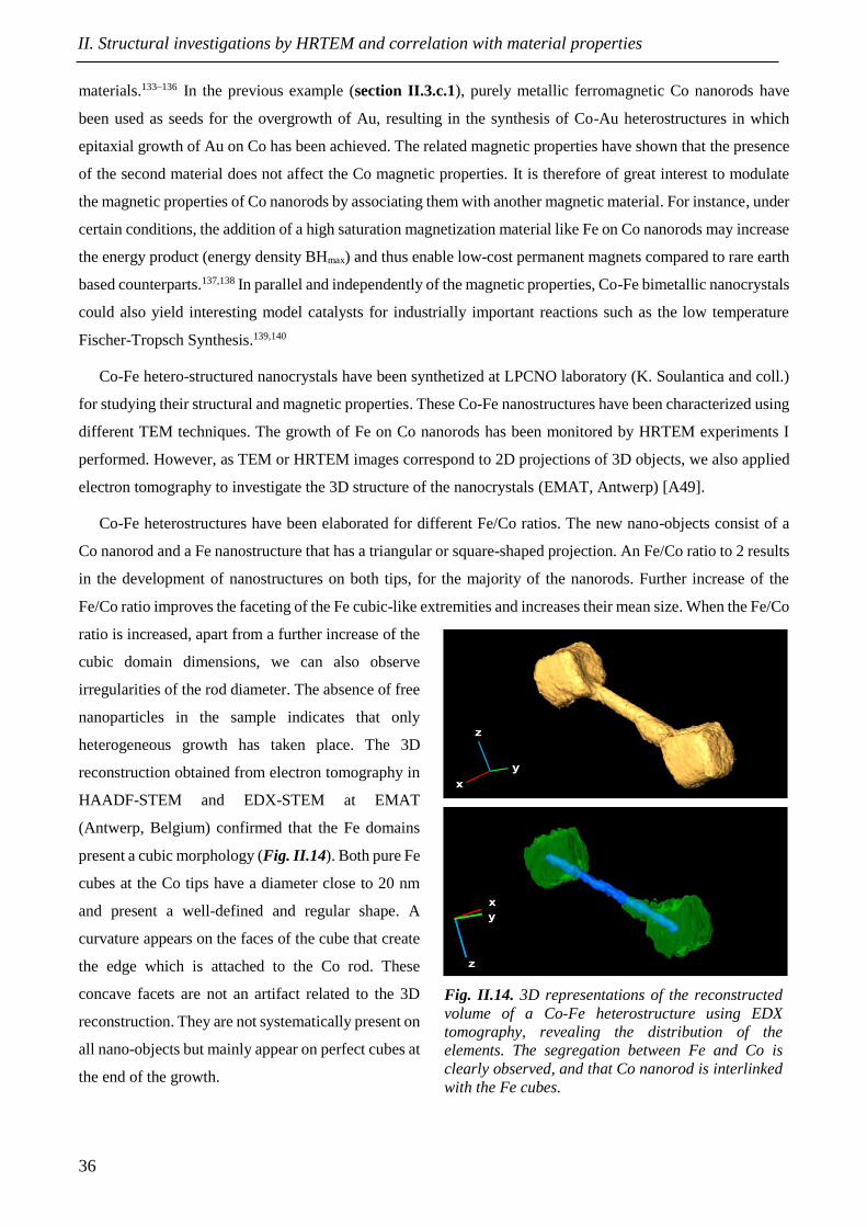
36
II. Structural investigations by HRTEM and correlation with material properties
materials.133–136 In the previous example (section II.3.c.1), purely metallic ferromagnetic Co nanorods have
been used as seeds for the overgrowth of Au, resulting in the synthesis of Co-Au heterostructures in which
epitaxial growth of Au on Co has been achieved. The related magnetic properties have shown that the presence
of the second material does not affect the Co magnetic properties. It is therefore of great interest to modulate
the magnetic properties of Co nanorods by associating them with another magnetic material. For instance, under
certain conditions, the addition of a high saturation magnetization material like Fe on Co nanorods may increase
the energy product (energy density BHmax) and thus enable low-cost permanent magnets compared to rare earth
based counterparts.137,138 In parallel and independently of the magnetic properties, Co-Fe bimetallic nanocrystals
could also yield interesting model catalysts for industrially important reactions such as the low temperature
Fischer-Tropsch Synthesis.139,140
Co-Fe hetero-structured nanocrystals have been synthetized at LPCNO laboratory (K. Soulantica and coll.)
for studying their structural and magnetic properties. These Co-Fe nanostructures have been characterized using
different TEM techniques. The growth of Fe on Co nanorods has been monitored by HRTEM experiments I
performed. However, as TEM or HRTEM images correspond to 2D projections of 3D objects, we also applied
electron tomography to investigate the 3D structure of the nanocrystals (EMAT, Antwerp) [A49].
Co-Fe heterostructures have been elaborated for different Fe/Co ratios. The new nano-objects consist of a
Co nanorod and a Fe nanostructure that has a triangular or square-shaped projection. An Fe/Co ratio to 2 results
in the development of nanostructures on both tips, for the majority of the nanorods. Further increase of the
Fe/Co ratio improves the faceting of the Fe cubic-like extremities and increases their mean size. When the Fe/Co
ratio is increased, apart from a further increase of the
cubic domain dimensions, we can also observe
irregularities of the rod diameter. The absence of free
nanoparticles in the sample indicates that only
heterogeneous growth has taken place. The 3D
reconstruction obtained from electron tomography in
HAADF-STEM and EDX-STEM at EMAT
(Antwerp, Belgium) confirmed that the Fe domains
present a cubic morphology (Fig. II.14). Both pure Fe
cubes at the Co tips have a diameter close to 20 nm
and present a well-defined and regular shape. A
curvature appears on the faces of the cube that create
the edge which is attached to the Co rod. These
concave facets are not an artifact related to the 3D
reconstruction. They are not systematically present on
all nano-objects but mainly appear on perfect cubes at
the end of the growth.
Fig. II.14. 3D representations of the reconstructed
volume of a Co-Fe heterostructure using EDX
tomography, revealing the distribution of the
elements. The segregation between Fe and Co is
clearly observed, and that Co nanorod is interlinked
with the Fe cubes.

37
II. Structural investigations by HRTEM and correlation with material properties
From the HRTEM images, we
clearly saw that the hybrid object
combines a single-crystalline Co
nanorod and a single-crystalline Fe
cube epitaxially grown on Co (Fig.
II.15). No Fe was detected on the Co
domains which are not encompassed
by the Fe cubes, which means that the
Fe detected by EDX and EELs is not
crystallized. The cobalt nanorods
penetrate into the iron nanostructures
without however protruding from
them. All epitaxial relationships
between Co and Fe have been
established thanks to Fast Fourier
Transform (FFT) patterns obtained
from different parts of the particle and
from several HRTEM images on different dumbbells. Fe and Co domains are linked by well-defined epitaxial
relationships meaning that the dumbbells can be considered as single-crystal structures with the Fe nanocubes
surrounding part of the Co nanorod. As expected, the growth axis of Co corresponds to the [0001] direction.
The zone axis of the Co part is the [2-1-10]. The planes that correspond to the surfaces enclosing the rod axis
correspond to the (01-10) (planes parallel to the rod axis). The Fe domains adopt a classical bcc structure and
are single crystals. The zone axis observed for the Fe part is [001]. The shape of the Fe nanostructures confirms
the one observed in electron tomography and can be well described as a parallelepiped presenting mainly the
{100} planes as surfaces with truncated edges exhibiting {110} facets. Considering the 4-fold symmetry of the
Fe part, we established that {111} planes appear at the corners. Based on all TEM results, a 3D model for the
nanostructures has thus been proposed.
HRTEM images have been analyzed by GPA method. The deformation of the Fe planes parallel to the Co
nanorod long axis has been measured to be -6,4% ±0.3 % (reference taken in the Co part) very close to the
theoretical mismatch between Co (01-10) and Fe (1-10), indicating that no epitaxial strain occurs and that Fe
seems perfectly relaxed on the surface of Co along this direction. Another interesting aspect concerning the
relations of the Co (2-1-10) and the Fe (001) planes is their quite important mismatch (-14.3 % with reference
to Co). This can be translated to a periodicity of 1 plane every 7. As a consequence one plane of Fe every seven
planes is in perfect coincidence with a plane of Co. This periodicity type is well known to favor the
crystallographic order and thus the epitaxy between different layers.141
In order to understand how growth occurs, we have examined by HRTEM the Fe/Co = 1/1 sample in which
dumbbells at different stages of Fe growth are present after 24h of reaction (Fig. II.16). The initiation of the
Fig. II.15. HRTEM image of a Fe-Co dumbbell and FFT patterns
obtained from Fe (up) and Co (down) domains of the dumbbell. A
shell layer can also be discerned mainly on the surface of Fe
domains, composed of oxide due to the exposition to the air.

38
II. Structural investigations by HRTEM and correlation with material properties
growth very close to the tips can be seen in structures in which only a limited amount of Fe is grown. The growth
initiation at this location is explained by the chemical accessibility of the surface of the nanorod. A part of the
nanorod tips is less effectively passivated by stabilizing ligands; therefore, the initial reaction of Fe takes place
at these positions. This configuration is not surprising since, as we have previously demonstrated, Au prefers to
grow on the extremes of Co nanorods when enough stabilizing ligand is available to cover efficiently the
nanorod lateral sides [A57]. Nevertheless, despite the fact that they grow close to the tips, the iron nanocubes
have a majority of interfaces with the lateral sides of the nanorods rather than with the tips. Indeed, Fe atom
deposition on the lateral sides of Co and subsequent growth by formation of (110) facets which grow on the rod
lateral facets seem to be favored against the formation of only a small interface on the tip. This diffusion along
the nanorod is not extended over the whole nano-rod length and iron growth preferentially continues by addition
of atoms on the already deposited iron layers along the nanorod lateral sides. Faceting develops as growth
advances. Some triangle shaped structures which correspond well to semi-parallelepipeds “cut” through their
diagonal have been observed. Subsequent growth continues around the nanorod and finally, the cube
encompasses the nanorod. The dimensions of the Fe structures depend on the Fe/Co ratio. However, we
observed that Fe can be found also away from the cubic domain towards the center of the nanorod.
Both the addition of different material and the shape modification can alter the magnetic properties of the
initial Co nanorods. Fe is a magnetically “soft” material in contrast to cobalt nanorods. The dumbbell shape
should also allow an easier magnetization reversal resulting in softer magnetic materials. The bare cobalt
nanorods exhibit high magnetic anisotropy, both due to their shape anisotropy (elongated shape) and to the
magnetocrystalline anisotropy of hcp-Co which acts along the hcp-c axis (the long rod axis). The hysteresis loop
of Co-Fe dumbbells showed that the magnetization evolves smoothly with the applied magnetic field indicating
an efficient exchange coupling between the two phases. The initial bare Co nanorods display a saturation
magnetization very close to the bulk Co. The bare cobalt nanorods exhibit a coercive field of about 0.5 T at
300K while for Co-Fe the value is decreased to 36 mT at room temperature. In order to have an insight into the
modification of the magnetic properties, 3D micromagnetic simulations have been performed for a single Co
nanorod and a Fe-Co dumbbell (see principle in section III.6.a). Introducing the nanorod shapes and dimensions
Fig. II.16. HRTEM images of dumbbells at different growth stages.(a) initial Fe deposition close to the Co
extremity; (b) growth of a Fe mainly on one side of the nanorod forming a trigonal prism; (c) the growth of
the second prism has started.

39
II. Structural investigations by HRTEM and correlation with material properties
deduced from the HRTEM analysis and using bulk magnetic parameters, micromagnetic simulations confirmed
the exchange coupling between Fe and Co phases, the increase in saturation magnetization and the decrease of
the coercive field due to the presence of Fe nanostructures. Since Fe is magnetically soft, the spin rotation is
facilitated at the Fe extremities of the dumbbells during the magnetization reversal. As a consequence, the hybrid
Co-Fe nano-object is softer than the bare Co nanorod, with a strongly reduced coercive field in comparison to
a bare Co nanorod.
This study is a last example of the interest to determine the structural properties by TEM for explaining the
magnetic properties of a localized nanosystem.
II.4. Conclusion
The study of structural properties by TEM, mainly using high-resolution mode, is one of my main research
axes. If for some years I focused my attention on experiments and developments in electron holography, I
continue to perform some structural investigations through different collaborations. Articles related to structural
studies by TEM represent about 50% of all my list of publications.
I have previously presented different studies of structural properties for various nanosystems, from
semiconducting quantum wells to hybrid magnetic nanoparticles. For each one, TEM studies did not consist
simply in obtaining nice images, but their analysis, even only qualitative, makes it possible to obtain valuable
information on the properties of the studied nanosystem, such as the formation interface, or the role of epitaxial
strain or defects on magnetic properties. However, it is necessary to assimilate and understand the context of
the study as well as the different properties of the nanosystem or its methods of synthesis. The best TEM
experiments and analysis will not be performed without knowing what we have to observe and how the sample
is illuminated by the electron beam.
I did not present other studies where I had less involvement or which correspond to occasional collaborations,
as some experiments performed for the French microscopy network (METSA). And it was also difficult to find
the common thread of all these works as many different systems have been studied: Co1-xNix/CoO core-shell
nanowires [A16], Co-Fe multilayers [A24], different Fe nanocubes [A25, A81], ultrafine-grained fcc/hcp cobalt
[A21], LaVo3/SrVO3 superlattices [A27]), ultrathin YSZ films on Si(001) [A31], alloys for aeronautic
application [A32, A41], Ag nanocrystals in amorphous matrix [A47], FePt nanoparticles [A52], epitaxial
MgO/Cr/MgO trilayers [A50, A65], growth of Co nanoparticles by the polyol process [A86].
. Obviously, the contexts of these studies are very different one from each of the others.
However, I would highlight a work not listed previously for which I had a lot of investment as the system
was as interesting as it was pleasant to study. In collaboration with L.M. Lacroix (LPCNO-INSA), I have
performed HRTEM experiments on Pt nanoparticles of unprecedented shapes for studying the fine-tuning
between growth mechanisms [A34]). We have demonstrated that quasi-monocrystalline Pt nanoparticles with
peculiar morphologies ( cubic dendrites, planar tripods, and fivefold stars) have been obtained selectively and
in high yield from a very simple procedure by tuning the reduction kinetics of a platinum salt under a dihydrogen

40
II. Structural investigations by HRTEM and correlation with material properties
atmosphere in the presence of an amine. The monocrystalline dendritic cubes present an outer cubic shape and
unprecedented size control of their envelope. Such dendritic cubes display a high surface-to-volume ratio, while
their cubic shape enables their self-assembly on surfaces, which should be of high interest in catalysis. The
synthesized fivefold stars showed multiply twinned arms with a disclination (a rotative dislocation) at the centre
of the particle (Fig. II.17). HRTEM experiments, in combination with electron tomography, allowed us to
determine the different faceted which composed the whole surface. This morphology is unique for Pt and could
open new perspectives for fundamental research on strained materials, as the study of the electrical properties
[A77]. In addition to this fundamental interest, catalytic activities could benefit from the presence of almost
exclusively crystallographic surface orientate on {111} for selectivity purposes.
Fig. II.17. (a) TEM micrograph of a single Pt fivefold star and (b) its corresponding
selected area electron diffraction pattern. HRTEM images of (c) the core and (d) a
branch tip as shown in (a) by white and black boxes, respectively.

41
III. Electric and magnetic field mapping using TEM
III. Electric and magnetic field mapping using TEM
As presented in the first part of this manuscript, I used the high-resolution mode in TEM during my PhD
thesis to study the structural properties of thin metallic layers (Ag, Au and Pt) and magnetic oxides (Fe3O4,
CoFe2O4, NiO) grown by sputtering, with the aim for elaborating an appropriate heterostructure and measuring
the spin dependence of specular electron reflections. The analysis of the structural properties of magnetic oxides
obtained by HRTEM made it possible to interpret a part of their magnetic properties. However, mapping
structural properties does not always provide information on these magnetic properties, and when the link
between properties exists, interpretation is not direct. Another possibility would be to directly map the magnetic
properties, i.e. the magnetic induction, at the nanoscale. In this case, TEM again remains the appropriate tool.
During my postdoc at CEA Grenoble (2004-2006) in the team of Pascale Bayle, I had to develop the magnetic
imaging in Fresnel and Foucault modes, techniques that did not exist in Grenoble. I thus discovered the
capabilities of TEM magnetic imaging, and the need to map and to quantify induction at the nanoscale, perfectly
complementary to structural properties studied in high resolution mode as well as other methods of magnetic
imaging or macroscopic magnetic measurements. However, the quantitative analysis of magnetic induction
maps is not direct and requires image processing that was not available. So I had to familiarize myself with the
development of software for data analysis, activity that I am still pursuing.
In the following, I will present the principle of magnetic imaging by TEM, from Lorentz microscopy (Fresnel
and Foucault modes) to electron holography. I will insist on this last method that I use and develop as my main
axis of research, and which is not limited to magnetic mapping as electrostatic potential can be analyzed,
opening the way to operando experiments on devices.
III.1. Introduction on magnetic mapping in TEM
The study of the magnetic properties of nanosystems requires the combination of macroscopic characterization
techniques which provide magnetic information averaged over large length scales with local techniques for
probing magnetic properties with high spatial resolution and sensitivity. Among the latter, magnetic imaging
techniques permit a direct study of the magnetic configurations, particularly magnetic domain structures at the
submicron scale. The possibility of imaging ferromagnetic order together with the improvement of the
computational time of micromagnetic simulations have significantly contributed to the understanding of the
magnetic phenomena at the local scale enabling the latest technological applications in the field of
nanomagnetism and spintronics. There is now a substantial number of magnetic imaging techniques as the Kerr
microscopy based on the magneto-optical Kerr effect (MOKE)142–144, the scanning electron microscopy with
polarization analysis (SEMPA)145–148, the spin-polarized low-energy electron microscopy (SPLEEM)145,
synchrotron radiation-based techniques such as x-ray magnetic circular dichroism, photoelectron emission
microscopy (XMCD-PEEM)149,150 and magnetic x-ray transmission microscopy (M-XTM)145 but also the
surface probe techniques such as magnetic force microscopy (MFM)151,152 and spin-polarized scanning
tunnelling microscopy (SP-STM).153 To finish, and I will detail them hereafter, TEM-based techniques such as

42
III. Electric and magnetic field mapping using TEM
Lorentz microscopy (LM) and electron holography (EH).148,154–156 All these experimental methods offer a wide
range of possibilities to study micromagnetic phenomena in different setups as can be seen in the comparative
list of their main features presented in Table III-1. Altogether they provide a spatial resolution ranging from
microns to few angstroms, a high sensitivity to detect small changes of the local magnetization, probing the
surface or the volume properties and sufficient versatility to enable the application of multiple external stimuli
(temperature, electromagnetic fields, etc.). None of these techniques covers all the possibilities, and they are
therefore complementary
Table III-1. Local techniques of magnetic mapping and their main characteristics.
From Table III-1, these methods of magneticc imaging can be classified following different criteria that
determine their range of application in terms of (spatial and time) resolution and sensitivity:
• The acquisition method: the image can be recorded using either a parallel acquisition of the signal at every
point of the image simultaneously (e.g. XMCD-PEEM, LM) or a serial acquisition in which a fine probe is
scanned across the sample (e.g. MFM, SP-STM).
• The probe-specimen interaction on which the magnetic contrast is based: the Lorentz force experienced by
electrons due to the magnetic induction of the sample or the Aharonov-Bohm effect (e.g. LM and EH); the
Technique Best spatial
resolution
(nm)
Information
depth (nm)
Acquisition
time (s)
Quantitative Type of
information
Type of
imaging
XMCD–
PEEM
20 2-20 0.03-10 Yes Surface Parallel
MXTM 20 Sample
thickness
(< 500nm)
3 Yes Volume Parallel-
scanning
Kerr
Microscopy
200 20 10-8 to 1 Yes Surface Parallel-
scanning
MFM 30 200-500 300 to 1800 No Surface Scanning
SEMPA 10 2 60-6000 Yes Surface Scanning
SPLEEM 20 1 1 Yes Surface Parallel
DPC 2 Sample
thickness
(<150 nm)
5-50 Yes Volume Parallel-
scanning
Lorentz
Microscopy
10 Sample
thickness
(< 150 nm)
0.04-30 Yes Volume Parallel
Electron
Holography
0.05 Sample
thickness
(< 150 nm)
>0.02 Yes Volume Parallel
SP-STM 0.02 0.2 30-1800 Yes Surface Scanning

43
III. Electric and magnetic field mapping using TEM
magnetic force on a magnetic tip caused by a stray field gradient (e.g. MFM); and magneto-optic coupling
between photons and the magnetization of the material (e.g. Kerr microscopy).
• The depth sensitivity, directly related to the probe-specimen interaction, determines whether the technique
is sensitive only to the sample surface (e.g. MOKE, SPLEEM) or to the whole volume of the specimen such
as in transmission techniques (e.g. M-XTM, LM and EH).
For the study of the local magnetic states, one of the most important requests is the achievable spatial
resolution. The TEM-based techniques are thus very interesting tools providing quantitative magnetic
information of the volume of the sample with flexibility to apply external stimuli (magnetic and electric fields,
injection of the electrical current, changes in temperature, stress, light, etc.) and a high spatial resolution.
Historically, the first attempts to study magnetic materials by TEM were to correlate the microstructure with
the magnetic domain configuration measured by other techniques. In 1957, Mayer157 established the first method
to map a magnetic signal adapting an electron mirror microscope. He observed artificial magnetic domain
patterns produced by an array of linear magnetic stray fields and the magnetic contrast of ferromagnetic barium
and nickel ferrite films. In 1959, Hale et al.158 developed the first methods to image domain patterns in
ferromagnetic thin films through defocused TEM imaging and thanks to the use of an off-centred objective
diaphragm to image magnetic domains.159 They established the basis of LM in Fresnel and Foucault mode
respectively. In the 1970s and 1980s, other TEM-based magnetic techniques such as phase contrast
microscopy160–162 and off-axis electron holography (EH)163,164 were developed. The basics principle of EH is
based on an original idea proposed by Gabor in 1949 to overcome the resolution-limiting spherical aberration
of the objective lens. 165, 166,167 But the electron beam phase shift measurements with sufficient sensitivity had
to wait for the development of high coherence electron sources which were available in commercial microscopes
in the ’80s. Tonomura made use of the off-axis electron holography to observe the fine structure of magnetic
domain walls163. The reconstruction of the hologram was made by an optical method using a Mach Zender
interferometer. Two years later, Tonomura observed the Aharonov-Bohm effect in permalloy magnets.168 EH
can thus be used to measure the corresponding phase shift of the electron wave to map the magnetic induction
as well as the electrostatic potential at the nanoscale.
III.2. The objective lens problem
The objective lens (OL) is the most important of the different lenses that constitute the electron microscope.
It forms the first image of the object and therefore determines the quality and the spatial resolution of the final
image. The OL, as all the lenses of the electron microscope, is an electromagnetic lens that creates a magnetic
field with a focusing effect on the electron beam. It is composed of a copper coil winded inside a cylindrical
magnetic yoke excited with a high electric current to generate an axial magnetic field. The pole pieces of the
yoke are designed to concentrate the flux lines in a small region where the electrons pass through the pole piece
gap.

44
III. Electric and magnetic field mapping using TEM
In a twin-type OL used in advanced microscopes, the specimen is placed just in the centre of the gap between
the pole pieces of two symmetric magnetic lenses, immersing the sample in a very intense and uniform magnetic
field (Fig. III.1). magnetic field seen by the sample can reach some Teslas (2 T for the Hitachi HF3300C).
Therefore, the magnetic field of the OL is sufficiently high to saturate most ferromagnetic materials, aligning
the magnetization almost parallel to the optical axis. This does not only alter the magnetic state of the specimen
but also minimizes the magnetic contrast because the TEM imaging techniques for magnetic mapping are only
sensitive to magnetic induction components perpendicular to the optical axis. Thus mapping the magnetic
configurations of materials cannot be performed in classical HRTEM conditions.
The OL has then to be switched off for TEM magnetic studies and other optical alignments of the microscope
have to be set in which the sample remains in a field-free environment. In dedicated TEM for magnetic imaging,
a special lens called Lorentz lens, located just below the OL and with a weak focusing power due to its very
weak magnetic field, is used in this case to magnify and form the image of the object without interacting with
the sample. This imaging mode called Lorentz mode can be used in EH as well as in LM, or for TEM
experiments which requires a large field of view, i.e. a low magnification. Due to its long focal length (few tens
of millimetres), the Lorentz lens has a large spherical aberration, degrading the spatial resolution to few
nanometers. Fortunately, recent developments in aberration correction set-ups have made possible to correct the
spherical aberration of the Lorentz lens, improving the spatial resolution down to 2 nm. Furthermore, recent
prototypes of dedicated Lorentz microscopes like the Hitachi HF3300C-I2TEM (In situ Interferometry TEM) I
used since 2012, designed between CEMES-CNRS and Hitachi High Technology, reaches a spatial resolution
of 0.5 nm in Lorentz mode. The solution proposed by Hitachi consists in adding another stage where the sample
can be introduced above the OL to guarantee field-free conditions, but keeping the OL on and a part of its
capabilities for the spatial resolution.
Fig. III.1. (a) Schematic representation of the magnetic field lines (dash red lines) inside a twin type
OL. (b) The column of I2TEM microscope (CEMES-CNRS). In the inset, Young fringes experiment
revealing the limit of the spatial resolution of the I2TEM in HRTEM mode (80 pm).

45
III. Electric and magnetic field mapping using TEM
III.3. Energy-loss Magnetic Chiral Dichroïsm
Among the TEM methods for magnetic measurements, only one of them does not require to have the OL
off. The energy-loss magnetic chiral dichroism (EMCD) method makes it possible to quantify the magnetic
moments and to retrieve the orbital over spin contribution to magnetism [A12]. This is the analog of the X-ray
magnetic circular dichroism applied in a TEM. EMCD thus allows measuring the component of the orbital over
spin magnetic moment contribution parallel to electron beam. The spatial resolution is determined by the
electron probe. However, the signal-to-noise ratio and the probe size strongly limit the achievable spatial
resolution. I mention this method used by few research groups in this manuscript because I collaborated with
B. Warot-Fonrose (CEMES), who leads this project, for developing software dedicated to data analysis from
EMCD experiments [A19].
The measurement of the dichroic signal in a TEM needs the recording of electron energy loss spectra at
precise locations in the diffraction pattern (Fig. III.2). Different experimental configurations are available to
combine spatial resolution and energy data. B. Warot-Fonrose developed the energy spectrum imaging (ESI)
method, also known as energy filtered TEM (EFTEM), applied in the diffraction plane. The whole diffraction
pattern is thus recorded for each energy slice to obtain a three-dimensional data set (two spatial dimensions and
the energy as the third one), called data cube.169 The advantages of the ESI method compared to other methods
are the ability to obtain a map of the dichroic signal and to correct for distortions or aberrations in a post-
treatment process.
Image treatments are necessary due to distortions, especially for drift and non-isochromaticity corrections. I
developed a full set of scripts in Digital Micrograph (Gatan) to measure and to remove all distortions from the
Fig. III.2. (a) Image of a data cube obtained using ESI method with the drawing of the
numerical masks used to extract the spectra presented in (b) from positions 1 and 2. (c)
Difference of the two spectra, i.e. dichroic signal.
b)
c)
a)

46
III. Electric and magnetic field mapping using TEM
datacubes and to extract reliable information. The key point is to measure and correct these distortions with
sufficient precision to extract the dichroic signal but at the same time to avoid any loss of meaningful
information. The measure and correction procedures were developed on an artificial data cube containing the
dichroic signal and some noise to prove the efficiency of the routines [A12]. These scripts were applied in real
systems for studying the dichroic signal in pure Fe thin films [P12] but also in FexCo1-x alloys as a function of
the Co amount [P11], or for optimizing the aperture sizes and positions in EMCD experiments [A14].
III.4. Lorentz Microscopy
III.4.a. Principle
From a classical point of view, LM is based on the Lorentz force (𝐹𝐿 ) that electrons moving with a velocity
𝑣 experience in a magnetic field �� :
𝐹𝐿 = −𝑒𝑣 × �� Eq. III.1
Considering that the electrons travel along the optical axis (z-axis), the vector product 𝑣 × �� indicates that
the Lorentz force induces a deflection of the electron trajectory only dependent on the component of the
magnetic induction perpendicular to the optical axis (�� ⊥ = �� (x, y)) (Fig. III.3 left-side). If the electrons go
through a thin sample of thickness t, its magnetic induction will deflect the electron trajectory an angle:
𝜃𝑳 =𝑒𝜆
ℎ𝐵⊥𝑡 = 𝐶𝐵⊥𝑡 Eq. III.2
where B⊥ is the magnitude of �� ⊥ and h is the Planck constant. C is a pre-factor that depends on the acceleration
voltage of the electron microscope, with an approximate value of 0.5 rad nm-1 T-1 for 300 kV. As an illustrative
example, a 10 nm thick cobalt film with a magnetic induction of 1.772 T (bulk value) will produce a deflection
angle of 0.086 mrad. The Lorentz deflection of thin film is about one or two orders of magnitude lower than the
typical Bragg diffraction angles produced by the low-index atomic planes (~5mrad).
In a quantum mechanical approach, if the electron beam is considered as a wave, the Lorentz force will be
described as a phase shift of the electron wave (Fig. III.3 right-side). The magnetic induction is then represented
by the vector potential inside the specimen, 𝐴 (𝑥, 𝑦)), and induces a phase shift on the scattered electrons,
according to equation :
𝜙𝑀𝐴𝐺(𝑥, 𝑦) = −𝜋𝛾
𝜆𝑈∗
𝑒
ℏ∫𝐴𝑧(𝑟 )𝑑𝑧 Eq. III.3
In focus, the image formation process in LM is similar to conventional TEM. The electron scattering process
induced by the magnetic sample creates a diffraction pattern in the back focal plane of the Lorentz lens due to
both the Bragg diffractions on the crystal lattice and the different “magnetic” beam deflections resulting of the
different magnetic induction directions lying in the sample. Without the effects of the spherical aberration of
the Lorentz lens (which is reasonable at low magnifications and weak scattering angle), the image intensity in
the image plane will only contain information concerning the amplitude. Magnetic contrasts in LM can thus

47
III. Electric and magnetic field mapping using TEM
only be obtained by altering the transfer function of the microscope. There are two ways to do that: defocusing
the image or using an aperture to select one deflected beam direction in the focal plane of the Lorentz lens.
These two methods define the two main LM modes: Fresnel and Foucault modes.148,155
The most popular method is the Fresnel mode (or out-of-focus mode). In this imaging technique, magnetic
contrasts due to magnetic domain walls (DWs) can be directly observed by defocusing the Lorentz lens in order
to image a plane either located above or below the sample plane (Fig. III.4.a). From a classical view, the
electron beam will be deflected in opposite directions thanks to the Lorentz force acting on the electrons when
passing through each side of a magnetic domain wall. It results in either an electron convergence or divergence
depending on the relative magnetization orientation in the two domains (Fig. III.4.a), producing respectively
bright or dark contrast lines. The wave behaviour associated with the electron beam results in the appearance of
interference fringes parallel to the domain wall separating two magnetic domains inducing the overlap of the
two beams. Fresnel contrasts thus appear only in defocused images.
In the second approach, called Foucault mode, the magnetic domains are imaged using an aperture located
in the back focal plane of the Lorentz lens to select a chosen magnetic deflection angle. Such aperture will only
let pass the electrons deflected by magnetic domains having the corresponding magnetic induction direction to
create the image. It will therefore result in a bright contrast associated with these domains. Electrons deflected
by domains of different magnetic induction direction are blocked and darker contrasts appear on the Foucault
image (Fig. III.4.b).
There is a third LM mode called differential phase contrast (DPC) microscopy. Contrary to Fresnel and
Foucault modes, the DPC is performed using a fine electron probe in a scanning transmission electron
microscope (STEM). The Lorentz deflection is measured on each point of the sample by a segmented STEM
detector when scanning the probe.162,170
Fig. III.3. Schematic illustration of the electron beam deflection due to the Lorentz force (left) and quantum
mechanical description (right) which lead to the overlap of beams coming from two different domains and the
apparition of interference fringes. Red and blue arrows represent the magnetization direction.

48
III. Electric and magnetic field mapping using TEM
Although Lorentz microscopy in Fresnel and Foucault modes offers the possibility to obtain a rapid and
direct visualization of DWs, both techniques only provide a qualitative analysis of the magnetic states. Van
Dyck et. al. solved this problem by applying to electron optics a non-interferometric approach to the phase
retrieval problem, originally developed in light optics, via the solution of the so-called Transport of Intensity
Equation (TIE).171 In the TIE method, the processing of a focal series of Lorentz images in Fresnel mode supplies
semi-quantitative information of the magnetic configuration of the specimen. This approach corresponds also
to inline electron holography which will not be detailed in the following.
III.4.b. Results
I started working on Lorentz microscopy during my postdoctoral internship at CEA Grenoble (2004-2006)
in the team of Pascale Bayle. The aim of my work was to implement both Fresnel and Foucault modes in a
JEOL 3010 microscope and to observe the magnetic properties of samples grown at CEA. After defining the
optical alignments of both modes in a field-free environment at the sample location, I started to develop shortly
afterwards an extension of the DPC technique adapted to conventional TEM for obtaining semi-quantitative
maps of the magnetic induction at different field values. This latter technique, so-called SIDPC (SI for Series
of Images), records series of images by moving the aperture or tilting the incident beam in ±X and ±Y directions
Fig. III.4. Schematic representation of the two imaging Lorentz microscopy modes: (a) Fresnel and
(b) Foucault modes. Red and yellow arrows located on the sample indicate the magnetization
direction of each magnetic domain.

49
III. Electric and magnetic field mapping using TEM
of the sample plane. It has been shown that adding the images in each direction produces two images linearly
proportional to BX and BY components respectively.172 The magnetic components are then computed with
respect to the origin of the incident beam (no magnetic deflection) and the vector map can be easily displayed
from the two images. In collaboration with A. Masseboeuf (Ph.D. student at that time), I implemented this
method on the JEOL 3010 microscope to perform in situ experiment magnetization for reversal process analysis.
The in-plane field applied to the sample was created by tilting the specimen holder in the axial magnetic field
of the objective lens (either residual field or field obtained by switching on the objective lens). Details on this
method are given in [A43]. These fields have been calibrated with a Hall-effect sensor.
I studied the exchange anisotropy of a polycrystalline Co35Fe65/NiMn bilayer. NiMn is widely used as an
AF layer for its high crystalline anisotropy field and high blocking temperature.173,174 For the LTEM observation,
the bilayer has been directly deposited by DC sputtering on carbon-coated thin film. Semi-quantitative maps of
the magnetic induction were obtained at different field values by SIDPC (Fig. III.5) [A18]. From the relative
intensity of magnetic maps, I calculated the local hysteresis loop of the bilayer. The curve showed the
appearance of an exchange-bias field of 30 Oe with two distinct reversal modes of the magnetization: the first
path corresponds to a reversal by wall propagation when the applied field is parallel to the anisotropy direction
whereas the second is a reversal by coherent rotation of magnetic moments when the field is applied antiparallel
to unidirectional anisotropy direction.
The SIDPC implantation required the development of software for controlling the beam tilt and the stage of
the microscope, but also for automatizing the acquisition and the data treatment. In particular, the long
Fig. III.5. Six magnetic maps obtained by SIDPC on the Co35Fe65(70 nm)/NiMn(50nm) bilayer. On
image (A) the unidirectional anisotropy direction is represented by the dashed white arrow. The inserted
color wheel indicates the direction of magnetization by the color and the intensity corresponds to the
strength of the magnetic signal. On image(C) some cross-tie walls are surrounded.

50
III. Electric and magnetic field mapping using TEM
acquisition time (~10 mn) for one magnetic map necessitated adapted procedure for correcting the sample drift
before processing the semi-quantitative maps. I thus had the opportunity to develop my skills in scripting using
Digital Micrograph.
My work on Fresnel and Foucault modes continued on the implementation of the TIE method with the
development of dedicated software for the reconstruction of the magnetic phase and data analysis. These
software have been used in different studies, mainly in collaboration with the “Institut of Nanoscience of
Aragon” (INA) at Zaragoza (Spain) [P6, A20, A37, A43, A53].
III.5. Off-axis electron holography: principle and data treatment
III.5.a. Principle
As previously described, when an electron beam passes through a material, the amplitude and phase of the
electron wave are modified due to different interactions. In conventional TEM imaging, the amplitude and phase
information are mixed and only the spatial distribution of the intensity (the square of the amplitude) of the
electron wave is recorded. While a single recorded image considered as a bright-field TEM image contains
information about the structure of the material, information about the phase of the electron wave function is
lost. Electron holography (EH) is an interferometric technique that allows recording directly the phase shift of
the high-energy electron wave that passed through a specimen. The phase shift can, in turn, be used to provide
information about local variations in the magnetic induction and electrostatic potential within and around the
specimen as seen in section I.3 (Eq. I.12)
The concept of electron holography was initially proposed and developed in 1948 by Denis Gabor who was
interested in overcoming electron microscope instrument limitations due to the unwanted aberration in
electromagnetic lenses.166,167 The type of holography initially proposed by Gabor is called inline holography,
but this one has for the most part been superseded by off-axis holography. A nice comparison between inline
and off-axis electron holography has been proposed by C. Koch.175,176
In off-axis EH, the phase shift of the electron
beam is recorded by performing an
interferometry experiment where the object
electron wave interferes with a reference
electron wave. A scheme of the off-axis EH
arrangement is displayed in Fig. III.6. The
resulting interference pattern, i.e. the hologram,
is a set of fringes with local periodicity
variations and shifts due to the relative
difference of the phase of the object wave and
the reference wave (Fig. III.7.a). The hologram
intensity and contrast are related to the Fig. III.6. Conventional TEM and off-axis EH schemes.
Fringes

51
III. Electric and magnetic field mapping using TEM
amplitude of the object wave 177, the beam coherence and its stability over the exposure time. To implement this
technique, the electron microscope requires the use of a high brightness and highly coherent electron source
associated with a Möllenstedt biprism to create the overlap of the two beams. 177 Particularly a high spatial
coherence and a high brightness of the electron source permit recording holograms with a very good fringe
contrast and intensity, up to recently limited to a short acquisition time of few seconds for avoiding specimen
and/or beam drift effects (see Project section P-II.1). The contrast or visibility is defined as 𝐼𝑀𝐴𝑋−𝐼𝑀𝐼𝑁
𝐼𝑀𝐴𝑋+𝐼𝑀𝐼𝑁 where
IMAX and IMIN are the maximum and the minimum values of the fringes. This parameter generally expressed in
% is usually between 5 % and 30 % and defined partly the signal-to-noise ratio.
The Möllenstedt biprism is usually a very thin Au-coated glass fibre or a Pt wire used to deflect both object
and reference electron wave to produce an overlap region that enables the interference phenomenon. Such
deflection is achieved by the application of a voltage on the biprism. Although there is an optimum geometric
arrangement of the biprism in the column of the microscope to obtain the highest hologram quality178, most
electron microscopes have to assemble it among the selected area apertures for technical reasons. As the
interference is produced between one electron wave that passes by the vacuum and another through the sample,
a vacuum area close to the sample is required for experimental constraints of overlapping, contrast value and
interfringe.
Mathematically, the hologram formation is described as follow. We consider two coherent waves
propagating along the direction z: the reference electron plane wave 𝜓𝑟𝑒𝑓(𝑟 ) = 𝐴𝑟𝑒𝑓(𝑟 )𝑒𝑖2𝜋�� ∙𝑟 and the object
electron wave 𝜓𝑜𝑏𝑗(𝑟 ) = 𝐴𝑜𝑏𝑗(𝑟 )𝑒𝑖[2𝜋�� ∙𝑟 +𝜙(𝑟 )]. 𝑟 = (x,y,z) is the position vector and �� the wave vector. The
action of the biprism makes that both reference and object electron waves are tilted with a certain angle (𝛼ℎ 2⁄
and −𝛼ℎ 2⁄ , respectively). Thus the intensity of the wave function for z=0 resulting from the interferences along
the 𝑥-axis is given by:
𝐼ℎ𝑜𝑙(𝑥, 𝑦) = 𝐴𝑟𝑒𝑓2 (𝑥, 𝑦) + 𝐴𝑜𝑏𝑗
2 (𝑥, 𝑦) + 2. 𝐴𝑟𝑒𝑓(𝑥, 𝑦). 𝐴𝑜𝑏𝑗(𝑥, 𝑦). cos [2𝜋𝛼ℎ
𝜆𝑥 + 𝜙(𝑥, 𝑦)] Eq. III.4
From Eq. III.4, we see that the hologram is formed by the conventional bright field image 𝐼𝐵𝐹 =
𝐴𝑟𝑒𝑓2 (𝑥, 𝑦) + 𝐴𝑜𝑏𝑗
2 (𝑥, 𝑦), superimposed over the sinusoidal term that represents mathematically the fringe
pattern of the hologram, and depends on both amplitude and phase shift 𝜙(𝑥, 𝑦) of the object wave (Fig. III.7.a).
Thus the hologram contains all the information of the object electron wave. The period of the interference
fringes, 𝜆 𝛼ℎ⁄ , depends on the deflection angle induced by the biprism voltage.
In the Fourier space, the hologram is represented by a central spot (central band) and two collinear spots
(sidebands) equally spaced with respect to the centre (Fig. III.7.b). The central band contains the conventional
bright-field image, while each sideband stores the information of the amplitude and phase. Choosing one of the
sidebands and performing the inverse Fourier transform allows extracting the object electron wave.

52
III. Electric and magnetic field mapping using TEM
III.5.b. Phase extraction and separation of the phase shift contributions
The reconstruction process starts calculating the fast Fourier transform (FFT) of a digitally recorded
hologram by a camera (CCD, CMOS, direct electron). Using a numerical mask with a defined shape (square,
cosine, Butterworth, Gaussian…), one of the sidebands is selected and then centred with respect of the FFT
image before calculating the inverse Fourier transform from the masked FFT. The amplitude and phase images
are then extracted from the resulting complex image. A summary of the phase reconstruction process of a
hologram recorded on a FeCo nanostar is represented in Fig. III.7.
In relation to the interferometric fringes, the phase image describes their shift or the variation of their
periodicity with respect to a reference area selected by the user (dotted white square in Fig. III.7.d). The size
(radius) of the numerical mask in the reciprocal space (FFT) is an essential parameter as it defines partly the
final spatial resolution and the signal-to-noise ratio of the amplitude and the phase images. In other words,
increasing the signal-to-noise ratio (smaller mask radius) is at the expense of the spatial resolution. We thus
need to find a good balance between the level of noise and the spatial resolution. The fringe space (𝑆𝑓) is the
other important factor for the spatial resolution of the reconstructed image.178
In any case, the recorded hologram, and consequently the resulting phase image, presents others phase shifts
than the one from the specimen. Indeed, the setup (microscope and detector) introduces phase shifts which have
in the most cases values higher than the ones to be investigated and prevent a clear analysis of the phase image.
These parasitic phase shifts come from the Fresnel fringes of the biprism and the distortions of projector lenses
and optical fibers for the camera with scintillator. The intensity of the resulting hologram becomes:
-
a) b)
c)
d)
50 nm
Fig. III.7. Process for amplitude and phase image extraction. (a)
Hologram of a FeCo nanostar with a zoom of fringes in the inset. (b)
Fast Fourier Transform (FFT) of (a) where a numerical mask is
applied on a sideband before be centred with respect to the FFT
image. (c) and (d) Amplitude and phase image calculated from the
inverse FFT of masked (b).

53
III. Electric and magnetic field mapping using TEM
𝐼ℎ𝑜𝑙(𝑥, 𝑦) = 𝐴𝑟𝑒𝑓2 (𝑥, 𝑦) + 𝐴𝑜𝑏𝑗
2 (𝑥, 𝑦) + 2. 𝐴𝑟𝑒𝑓(𝑥, 𝑦). 𝐴𝑜𝑏𝑗(𝑥, 𝑦). cos [2𝜋𝛼ℎ
𝜆𝑥 + 𝜙(𝑥, 𝑦) + 𝜙µ(𝑥, 𝑦)] Eq. III.5
where 𝜙µ(𝑥, 𝑦)represents the sum of parasitic phase shifts. It is then mandatory to record a reference hologram
in a field-free vacuum area which will contains only 𝜙µ(𝑥, 𝑦). The phase image of this reference hologram is
extracted following the same procedure and same parameters as the initial hologram and is subtracted to the
sample one for removing phase from the setup (Fig. III.8.a and b.).179
The extracted phase image has values between –π and +π and phase discontinuities or phase jumps appear
at positions where the phase exceeds this amount (wrapped image). The phase image can be “unwrapped” using
some suitable algorithms to remove the phase jumps and to obtain a continuous variation of the phase shift (Fig.
III.8.c).180
We have seen in section I.3 that the phase shift from the specimen contains different electromagnetic
contributions which correspond to a projection and an integration of the corresponding potential/field along the
electron path:
𝜙(𝑥, 𝑦) = 𝐶𝐸 ∫𝑉(𝑟 )𝑑𝑧 −𝑒
ℏ∬𝐵⊥(𝑟 )𝑑𝑟𝑑𝑧 Eq. III.6
The first one, the electric phase shift 𝜙𝐸𝑙𝑒𝑐, corresponds to the electrostatic potential and the second one, the
magnetic phase shift 𝜙𝑀𝑎𝑔, to the magnetic induction. 𝜙𝐸𝑙𝑒𝑐 is related to the atomic potential (mean inner
potential or MIP) and/or the presence of an excess of electric charges. In the following, we will then separate
𝜙𝐸𝑙𝑒𝑐 in two sub-contributions, 𝜙𝑀𝐼𝑃 and 𝜙𝐶ℎ𝑎𝑟𝑔𝑒𝑠, for distinguishing the origin of the electric potential (atomic
or excess of charge respectively). 𝜙𝑀𝐼𝑃 is always present when observing a material, while 𝜙𝐶ℎ𝑎𝑟𝑔𝑒𝑠 appears
only if an excess of charges creating an electric field exists. If the sample possesses magnetic properties with a
non-zero in plane magnetic induction, 𝜙𝑀𝑎𝑔 will contribute to the total phase shift. The total phase shift can
then be expressed as a linear combination of each potential contribution given by:
𝜙 = 𝜙𝐸𝑙𝑒𝑐 + 𝜙𝑀𝑎𝑔 = 𝜙𝑀𝐼𝑃 + 𝜙𝐶ℎ𝑎𝑟𝑔𝑒𝑠 + 𝜙𝑀𝑎𝑔 Eq. III.7
- 8.5 rad 0
a) b) c)
50 nm
Fig. III.8. (a) Phase image extracted from a reference hologram recorded in vacuum and showing phase
distortions coming from the set-up (microscope and camera). (b) Phase image calculated from Fig.
III.7.d after subtracting (a). (c) Unwrapped phase image of (b).

54
III. Electric and magnetic field mapping using TEM
For studying independently the different contributions, it is necessary to separate them. However, separating
𝜙𝑀𝐼𝑃 and 𝜙𝐶ℎ𝑎𝑟𝑔𝑒𝑠 is quite complicated as they come from the same physical potential even if this potential
can have different origins (𝑉𝑀𝐼𝑃 and 𝑉𝐶ℎ𝑎𝑟𝑔𝑒𝑠). In some cases, if the sample width (e.g. the thickness seen by
the electron beam) is constant and the chemical composition is homogeneous over the studied area, the phase
variations can be related only to 𝜙𝐶ℎ𝑎𝑟𝑔𝑒𝑠 as 𝜙𝑀𝐼𝑃 keeps a constant value. Otherwise a precise knowledge about
the thickness and 𝑉𝑀𝐼𝑃values are required, or 𝑉𝐶ℎ𝑎𝑟𝑔𝑒𝑠 has to be modified in two successive holograms thanks
to in situ/operando experiments and a relative 𝜙𝐶ℎ𝑎𝑟𝑔𝑒𝑠 can be calculated by subtracting the corresponding
phase images as 𝜙𝑀𝐼𝑃 remains unchanged.
Extracting 𝜙𝑀𝑎𝑔 from the total phase shift is less complicated. Several procedures exist; some of them are
more or less suitable depending on the magnetic behaviour of the sample and their implementation. The two
main procedures are:
• Saturation the sample magnetization in two opposite directions: Two holograms are recorded after saturating
the magnetization of the sample in two opposite in-plane directions. 177 This method requires either the use of a
dedicated magnetizing holder or the conventional objective lens after tilting the sample to switch and saturate
the magnetization in opposite directions. Perfectly antiparallel saturation states induce a change of the sign in
the magnetic phase shift contribution keeping constant the electrostatic contribution. This method is very useful
in nanostructures with high in-plane shape anisotropy (e.g. nanowires, nanostripes…) where the magnetostatic
energy confines the magnetization in specific and stable orientations. But non saturated magnetic states, in
particular magnetic walls separating magnetic domains or vortices, cannot be studied.
• Switching upside down the sample: This method can be applied in almost all the cases, and this advantage
explains why it is the most used method. It was proposed by Tonomura considering the “time-reversal operation
of the electron beam”,181 where the sign of the magnetic phase shift contribution is changed by flipping the
sample while the electrostatic phase shift (a scalar) remains constant. It consists in recording two holograms
where one of them is taken after manually flipping the sample upside down. The phase image resulting from
the first experiment is called “phase up”, and the second one is “phase down”. After numerical alignment
procedure, the half sum and the half subtraction of both phase images are computed resulting in two new phase
images corresponding to the main inner potential (MIP) if any 𝜙𝐶ℎ𝑎𝑟𝑔𝑒𝑠 is present and the integrated magnetic
induction (MAG) respectively (Fig. III.9). By this way, the magnetic state of the specimen is not altered. But
the main drawback is the numerical realignment of the up ond down phase images for correcting their relative
shift and rotation before computing the half sum and the half difference.

55
III. Electric and magnetic field mapping using TEM
Others procedures as changing the electron acceleration voltage, or taking two holograms at different
temperatures (above and below the Curie temperature)182–184 exist but are difficult to perform and consequently
very rarely used.
III.5.c. Quantification from phase images
The in-plane components of the electric and magnetic fields integrated along the electron path can be
obtained from the corresponding phase images. For the electrostatic phase shift, the isophase lines correspond
to isopotential lines: consequently, the integrated electric field is perpendicular to the isophase lines. The
projected magnetic induction can be directly observed following the isophase lines (Fig. III.10.a). The cosine
of the phase image which can be amplified by a numerical factor allows highlighting the isophase contours and
the corresponding direction of the magnetic induction (Fig. III.10.b) or the distribution of the electric potential.
The density of isophase lines is directly related to the amplitude of the integrated field.
More specifically, the in-plane components integrated along the electron path can be computed using the
derivative function of the phase shift. For the electric field which appears if a variation of the potential occurs,
its integrated in-plane components correspond to:
∫𝐸𝑥(𝑥, 𝑦, 𝑧)𝑑𝑧 = −1
𝐶𝐸
𝜕𝜙𝐶ℎ𝑎𝑟𝑔𝑒𝑠(𝑥,𝑦)
𝜕𝑥 and ∫𝐸𝑦(𝑥, 𝑦, 𝑧)𝑑𝑧 = −
1
𝐶𝐸
𝜕𝜙𝐶ℎ𝑎𝑟𝑔𝑒𝑠(𝑥,𝑦)
𝜕𝑦 Eq. III.8
Similarly, the integrated in-plane components of the magnetic induction are equal to:
∫𝐵𝑥(𝑥, 𝑦, 𝑧)𝑑𝑧 =ℏ
𝑒
𝜕𝜙𝑀𝐴𝐺(𝑥,𝑦)
𝜕𝑦 and ∫𝐵𝑦(𝑥, 𝑦, 𝑧)𝑑𝑧 = −
ℏ
𝑒
𝜕𝜙𝑀𝐴𝐺(𝑥,𝑦)
𝜕𝑥 Eq. III.9
Up
Down
MIP
MAG
50 nm
-
+
-
Fig. III.9. Separation of the mean
inner potential (MIP) and magnetic
(MAG) contributions to the phase
shift. MIP and MAP images result of
the half sum or half subtraction
respectively of up and down
observations after switching the
sample and numerical alignment.

56
III. Electric and magnetic field mapping using TEM
In some cases, the field is assumed to be homogeneously distributed along the electron path on a constant
thickness w corresponding to the lamella width crossed by the electron beam. Electric and magnetic in-plane
components can thus be obtained with the following equations:
𝐸𝑥(𝑥, 𝑦) = −1
𝑤.𝐶𝐸
𝜕𝜙𝐶ℎ𝑎𝑟𝑔𝑒𝑠(𝑥,𝑦)
𝜕𝑥 and 𝐸𝑦(𝑥, 𝑦) = −
1
𝑤.𝐶𝐸
𝜕𝜙𝐶ℎ𝑎𝑟𝑔𝑒𝑠(𝑥,𝑦)
𝜕𝑦 Eq. III.10
𝐵𝑥(𝑥, 𝑦) =ℏ
𝑤.𝑒
𝜕𝜙𝑀𝐴𝐺(𝑥,𝑦)
𝜕𝑦 and 𝐵𝑦(𝑥, 𝑦) = −
ℏ
𝑤.𝑒
𝜕𝜙𝑀𝐴𝐺(𝑥,𝑦)
𝜕𝑥 Eq. III.11
For magnetic materials, some magnetic configurations lead to an equivalence between induction and
magnetization (for instance for induction parallel to the wire axis or in the plane of thin films). In-plane
components of the magnetization Mx and My are thus quantitatively measured:
𝑀𝑥(𝑥, 𝑦) =∫𝐵𝑥(𝑥,𝑦,𝑧)𝑑𝑧
𝜇0.𝑤 and 𝑀𝑦(𝑥, 𝑦) =
∫𝐵𝑦(𝑥,𝑦,𝑧)𝑑𝑧
𝜇0.𝑤 Eq. III.12
A quantitative vector map can be computed from both components for each field. An example of magnetic
components using Eq. III.9 is given in Fig. III.10.c and d. The vector map is in general represented using colors
where the color and its intensity give respectively the direction and the amplitude of the field (Fig. III.10.e).
The color-coded vector map can also be modulated by the cosine of the phase image to highlight the induction
lines (Fig. III.10.f). Arrows can also be drawn. The vector map representation of the field calculated from the
phase image is often more clearly understood, especially for magnetic materials where the vector potential is
a) c) e)
f) d) b
)
BX
BY
50 nm
Fig. III.10. (a) Isophase lines parallel to induction lines calculated from MAG (Fig. III.9). The step
between the isophase lines is equal to 0.09 rad. (b) Cosine of MAG with an amplified factor of 15. (c)
and (d) X and Y components of the MAG calculated using Eq. III.9. (e) Vector map calculated from (c)
and (d). The color and its intensity give respectively the direction and the amplitude of the field as seen
on the color wheel. (f) Combination of (b) and (e).

57
III. Electric and magnetic field mapping using TEM
never used to represent their magnetic configuration. For example, micromagnetic calculations always give the
components of magnetic induction (see section III.6.a). However the vector map representation presents a
major drawback: it requires calculating the gradient of the phase shift, and therefore to strongly decrease the
signal-to-noise ratio. Noise can be filtered by adequate spatial filters, but always at the expense of spatial
resolution. For this reason, it is preferable to calculate the phase image to be compared with the experimental
phase image from the simulated components, and not to derive the experimental phase image for a comparison
with the simulated integrated components. The calculation of the simulated phase image from components is
explained in section III.6.a.
III.5.d. A dedicated microscope
I performed my first EH experiments on a FEI Tecnai F-20 microscope acquired in 2004. This microscope
was the first one installed with a commercial corrector for the spherical aberration of the objective lens and was
dedicated to high-resolution experiments (section II) with a spatial resolution of 0.12 nm. It is equipped with a
Schottky field emission gun and a single biprism allowing EH studies. If no dedicated Lorentz lens is present,
the first transfer lens of the corrector (TL11 lens) was used for this purpose while switching off the objective
lens. A special setting of the corrector developed at CEMES with the CEOS company has limited the
deterioration of the spatial resolution which reaches nevertheless about 5 nm.
In 2012, a Hitachi HF 3300C, so-called I2TEM for “In situ Interferometric TEM”, was installed for electron
holography experiments. This 300kV microscope has been specially designed to perform in situ and
interferometric experiments with very stable mechanical setup and electronics power supply to optimize the
stability and the signal-to-noise ratio. Associated to a cold field emission source for very high spatial and
temporal coherences, two goniometers are available on the column: one of them is called Lorentz stage and is
located above of the objective lens, where the sample can be in real magnetic field-free position and the other
one is the normal stage in which the sample is located in the middle of the OL. Using the Lorentz stage (Lorentz
mode) allows performing experiments for magnetic imaging or for studies requiring a large field of view while
keeping the objective lens as Lorentz lens. The normal stage corresponds to conventional and high-resolution
TEM. It is however possible to switch off the OL and to use the TL11 lens of the corrector for having another
Lorentz mode similar to the Tecnai one. This microscope has a spherical aberration corrector (CEOS B-COR
Aplanator) dedicated to large field of view modes allowing reaching a spatial resolution down to 0.5 nm in both
Lorentz modes. Four rotatable electrostatic biprisms have been installed, the first one (condenser biprism BPC)
below the gun and the others (BP1 to BP3) in the imaging part. In most cases, I have used BP1 and BP2 at the
same time in a “double biprism configuration”185 to avoid artefacts linked to Fresnel fringes and to set separately
the interference area size 𝑊 and the fringe spacing 𝑆𝑓. The condenser biprism allows splitting the electron beam
in two parts for increasing the distance between the object and the reference wave at the object plane.186–188 But
this feature is difficult to realize and additional work is needed for developing the corresponding optical
alignment (see Project section PII-2).

58
III. Electric and magnetic field mapping using TEM
Finally, “large” sample holders can be introduced to perform various in situ experiments. For this purpose,
different sample holders have then been acquired:
• Biasing holder with 9 contacts and dedicated chips.
• 4 electrical contacts with high and low temperatures holder (-150 °C to 250 °C).
• Nano-indentor holder equipped with a nanoscale conductive tip with piezoelectric displacement.
• Magnetizing holder to apply a local magnetic field (300 Oe in the sample plane).
III.5.e. Off-line and live data treatments: qHolo & HoloLive!
The major drawback of EH is the need to extract and manipulate the useful signal, i.e. the phase image. The
extraction of the phase image includes several delicate calculation steps while the quantification and the analysis
of the electromagnetic potentials needs special procedures as the separation of the phase shift contributions or
the calculation of the vector map. The acquisition of holograms is thus only the first step of a full holographic
experiment and has to be conducted in relation with the different steps of data treatment. For instance, the
interfringe and the interference area will determine the spatial resolution and the field of view of the phase image
while the exposure time and the visibility of fringes will act on the signal-to-noise ratio, and consequently on
the size of the numerical to be applied, related to the spatial resolution…
The procedure detailed in section III.5.b for obtaining a magnetic phase image is summarized thereafter:
• Extraction of phase and amplitude images from the “object” hologram “up”.
• Extraction of the phase image of the reference hologram with the same parameters (type, position and
mask size).
• Subtraction of two phase images for removing the distortions of the microscope and detector.
• Choice of a reference area on the phase image.
• The first four steps are repeated for the "object" hologram “down” acquired after flipping back the
sample.
• Alignment of “up” and “down” phase images to correct the relative rotation and shift (and possibly
magnification variations).
• Subtractions of “up” and “down” phase images to isolate the magnetic contribution.
Then the phase image analysis can follow these steps (see section III.5.c)
• Application of a cosine, or a procedure to display isophases with a defined step.
• Remove of phase jumps (unwrapping) for drawing profiles and/or calculating gradient.
• Spatial filtering to suppress high frequency noise.
• Application of the gradient to obtain both in-plane components.
• Calculation of the color-coded vector map.
All these steps are conducted for a single magnetic configuration and for a defined area of an object. If a
larger field of view is needed, or if several holograms are recorded on the same area as a function of stimulus
for an in situ experiment, all the treatment steps will have to be repeated on each acquired hologram.

59
III. Electric and magnetic field mapping using TEM
The main difficulty encountered by research groups that start an EH activity concerns the means available
to process the data. It exists only one commercial software which does not allow a full control and a clear
understanding of the different steps of the data treatment. Most of the recognized groups in this field have then
developed their own code they keep for their own use. Concerning the CEMES laboratory, the EH studies started
in 2004 after the acquisition of the Tecnai F20 microscope making possible to carry out such experiments. The
first holograms were treated using the GPA software as the procedure for extracting the phase image from an
hologram is similar to the one for studying the atomic displacement from HRTEM images. But this software
was adapted neither to an automatic procedure for treating several holograms in the same batch as required for
performing in situ experiments, nor to a full quantification of the electromagnetic contributions of a phase image.
In addition, it did not allow numerical alignment of images in shift and rotation. More importantly, the non-
direct visualization of the phase signal in the hologram prevented to optimize and succeed the in situ
experiments. Without phase visualisation during experiments, it is not possible to determine if the data being
collected is valuable and if the applied stimuli are indeed changing the expected signal in the case of in situ
studies.
I decided to solve these bottlenecks to fully exploit the huge possibilities offered by
EH for studying the electromagnetic properties of nanostructures, in particular through in situ/operando
experiments. I thus focused my efforts these last 10 years on the development of software allowing an automatic
and fast treatment of series of holograms for a direct visualization and accurate quantification of the signal. Two
software have then been developed under Digital Micrograph (Gatan): qHolo and HoloLive!.
qHolo is dedicated to a post-treatment of series of holograms, from the phase
and amplitude extraction to quantification of the magnetic induction or elementary
charge mapping (see section III.7.a). qHolo is divided into different parts allowing
to follow the full procedure in an intuitive way.
HoloLive! is designed to help the user during EH experiments by providing live
phase images with automatic removal of distortions from the setup and tools for a
first analysis of the signal. It allows an automatic detection and a tracking of the
side-band, a live phase unwrapping with an handy window for controlling
procedures and output (Fig. III.11). In addition of its capabilities for selecting the
data to be acquired and for succeeding in in situ/operando experiments, this
software can also be used to measure the position of the hologram fringes in real-
time from the live phase images, allowing feedback control of the microscope (see
Project section P-II.1) .
I will not detail in the following all the capabilities of these software. Their short descriptions do not reflect
the time I spent developing them and the key role they had for all studies presented in the next parts of the
manuscript. To finish, HoloLive! is commercialized by HREMResearch (https://www.hremresearch.com/)
since 2019 and qHolo will be soon available on the same platform.
Fig. III.11. Main
window of HoloLive!.

60
III. Electric and magnetic field mapping using TEM
III.5.f. Double exposure
The operando EH experiment on the magnetic field produced by the write pole of a hard disk drive head as
a function of applied electrical current gave me the opportunity to develop a new interferometric method
allowing a quantitative analysis of the magnetic and electric properties emanating from objects using holograms
free of artifacts and with a frequential sensitivity [A69]. All details about the operando study are given in section
III.6.e. This new method called Dynamical Holographic Moirés (DHM) was implemented in a TEM in
collaboration with A. Masseboeuf (CEMES).
A Moiré pattern consists in interference fringes resulting from the superimposition of two spatial periodic
structures. As a result, a modulation of the image intensity appears within the pattern. A simple distinction
between Moiré pattern and EH can be drawn by the part of the wave under interest: Moiré fringes appear as
changes in the amplitude of the exit electron wave while EH aims at retrieving the full exit wave, mostly
focusing on its phase part. Moiré patterns have intensively been used in TEM for decades for the study of lattices
deformation due to stacking faults189, crystal orientation190 or dislocations.191
The DHM method combines EH and Moirés patterns for performing frequency studies of the electromagnetic
field. The principle of DHM is to superimpose two holograms obtained on the same area of an object which is
periodically stated in two different but controlled configurations (either electrostatic or magnetic). The
overlapping of both holograms gives rise to Moiré contrasts in the final amplitude image carried out by the
fringes of the holograms.
The addition of two interferometric patterns corresponding to a double exposure was already proposed in
optical interferometry and was formerly used in a photonic bench. It enabled to access variations of gas
distribution during an arc discharge or to the macroscopic deformation of a given object under external stress.
192,193 In 1987, its first implementation in a TEM was applied to off-axis EH experiments on electromagnetic
fields.194–197 The double exposure technique presents different advantages. First at all, the signal can be directly
visualized and interpreted from the recorded image by observing the modulation of the amplitude of fringes.
Secondly, it is not necessary to correct the final image for any perturbations of the reference wave (as it has to
be done for EH, see section III.5.b) as these perturbations do not contribute to the modulated amplitude if they
remain the same for both holograms which will be overlapped. Finally, the Moiré contrasts linked to the relative
signal between both holograms are not influenced by the distortions originating from the microscope setup
(projector lens, camera...) as they remain identical for all images recorded at the same magnification. Double
exposure EH has been further developed by various groups to improve the phase sensitivity.198–201 However, the
main drawback of this method is a lower spatial resolution and a lower sensitivity to weak signals compared to
the ones obtained in off-axis EH. In addition, the superimposition between both holograms requires to necessary
record the holograms with identical conditions. The emergence of computational hologram treatment, as well
as the great improvement of detectors, turned out this technique less used with respect to achievable modern
methods (Fourier analysis) which are less time consuming for an improved sensitivity.
The DHM method is depicted by an illustration using the calculated electrostatic field from a virtual charged
sphere which can be modulated between a positive and negative state (Fig. III.12). The only feature required

61
III. Electric and magnetic field mapping using TEM
in our experiment is to be able to switch the charge state of the sphere without any other modification of the
optical system during the acquisition time. The phase shift 𝜙𝑠(𝑥, 𝑦) related to the positive charge state is shown
Fig. III.12.a. However, the experimental setup (microscope and detector) creates additional parasitic phase
shifts 𝜙µ(𝑥, 𝑦) which can strongly modify the expected signal (Fig. III.12.b). The intensity of the hologram
resulting from the overlap along the 𝑥-axis parallel to the biprism between the beam which crossed the sample
s and the one through the vacuum can be written as:
𝐼𝐻𝑠(𝑥, 𝑦) = 𝐴02(𝑥, 𝑦) + 𝐴𝑠
2(𝑥, 𝑦) + 2. 𝐴0(𝑥, 𝑦). 𝐴𝑠(𝑥, 𝑦). cos [2𝜋𝛼ℎ
𝜆𝑥 + 𝜙𝑠(𝑥, 𝑦) + 𝜙µ(𝑥, 𝑦)] Eq. III.13
The hologram in Fig. III.12.c displays a fringe deformation coming from 𝜙𝑠(𝑥, 𝑦) due to the electric field
generated by the sphere. 𝜙𝑠(𝑥, 𝑦) is usually extracted by Fourier filtering while the phase distortions 𝜙µ(𝑥, 𝑦)
coming from the setup are removed recording a reference hologram in the vacuum (see section III.5.b). Fig.
III.12.d shows the same hologram for an opposite charge.
In the double exposure method, the recorded image (interferogram) corresponds to the simple addition of the
half intensity of both previous holograms where s1 and s2 describe two different charge states, here opposite
states with s1 = - s2. Assuming that the amplitude of the object wave is not modified between both charge states,
i.e. 𝐴𝑠1(𝑥, 𝑦) = 𝐴𝑠2(𝑥, 𝑦), the intensity of the final interferogram in Fig. III.12.e is:
𝐼𝐷𝐻𝑀(𝑥, 𝑦) =1
2(𝐼𝐻𝑠1(𝑥, 𝑦) + 𝐼𝐻𝑠2(𝑥, 𝑦))
Fig. III.12. (a) Phase image simulation of a sphere
with a positive charge of 100 e (field of view equal to
1 μm). (b) Phase image simulation of the same
sphere including experimental phase distortions due
to the microscope setup. (c) and (d) Simulated
holograms for a positive and negative charge
respectively. (e) Double exposure hologram
(interferogram) corresponding to the addition of the
two previous hologram. (f) Electrostatic map
obtained from the amplitude analysis of the
interferogram in (f ).

62
III. Electric and magnetic field mapping using TEM
= 𝐴0,2 (𝑥, 𝑦) + 𝐴𝑠1
2 (𝑥, 𝑦) + 2. 𝐴0(𝑥, 𝑦). 𝐴𝑠1(𝑥, 𝑦). [cos [2𝜋𝛼ℎ
𝜆𝑥 + 𝜙𝑠1(𝑥, 𝑦) + 𝜙µ(𝑥, 𝑦)] +
cos [2𝜋𝛼ℎ
𝜆𝑥 + 𝜙𝑠2(𝑥, 𝑦) + 𝜙µ(𝑥, 𝑦)]] Eq. III.14
which can be rewritten into:
𝐼𝐷𝐻𝑀(𝑥, 𝑦) = 𝐴0,2 (𝑥, 𝑦) + 𝐴𝑠1
2 (𝑥, 𝑦) + 2. 𝐴0(𝑥, 𝑦). 𝐴𝑠1(𝑥, 𝑦). cos [𝜙𝑠1(𝑥,𝑦)−𝜙𝑆2(𝑥,𝑦)
2] . cos [2𝜋
𝛼ℎ
𝜆𝑥 +
𝜙𝑠1(𝑥,𝑦)+𝜙𝑠2(𝑥,𝑦)
2+ 𝜙µ(𝑥, 𝑦)] Eq. III.15
This simple mathematical description shows that the amplitude of the holographic fringes is modulated by
the cosine of the phase difference 𝜙𝑠1(𝑥, 𝑦) − 𝜙𝑆2(𝑥, 𝑦) between both superimposed states. This cosine term
then corresponds to the envelop function of these holographic fringes and is the origin of the Moirés contrasts.
It is interesting to note that this term does not depend on the holographic fringe periodicity i.e. the applied
voltage on the biprism. On Fig. III.12.e, we can clearly observe the appearance of the Moirés pattern which can
be emphasized by the use of a classical Fourier filtering on the fringe frequency equivalent to the amplitude
image (Fig. III.12.f). The shape of the Moirés pattern within the interferogram only represents the variation of
the electrostatic potential (equal to twice the electric field) emanating from the charged sphere, while the phase
distortions due to the microscope optic and the camera have been removed. As a consequence, the interferogram
contains a quantitative information on the relative variation of the magnetic or electric potential between two
defined states without any contribution from any other phase terms remaining constant during such variation.
The distance between two maxima (white lines) or two minima (black lines) corresponds to a difference of one
period of the holographic fringes between both superimposed holograms, i.e. a phase shift of 2π coming from
the presence of an electromagnetic field. The experimental challenge to perform successfully such DHM
experiment relies on the ability to quickly vary and control the electromagnetic field for making an addition of
at least two defined states during the acquisition time, keeping the whole optical alignment stable without any
change. Microelectronics devices whose state can be tuned in two controlled configurations by an external
alternative input of various frequencies are perfect systems to be studied by DHM. Any defined state can then
be studied with any frequency.
With A. Masseboeuf, we had the idea to develop and implement this method studying the magnetic field
emanating from the writing pole of a hard drive disk head [A69]. Indeed, the magnetic flux created by the pole
was controlled by the applied current into the coils (see section III.6.e and [A59]). It was then possible to inject
either a positive or a negative DC current through the coil of the pole during EH experiment. Recording
holograms with opposite currents allowed us to access to the intrinsic writer pole magnetic flux and the intrinsic
magnetic shield contribution respectively. Fig. III.13.a presents the hysteresis loops of the horizontal
component (i.e. perpendicular direction to the surface of the pole) of the projected magnetic inductions for the
pole and the surrounding shield. They have been calculated from an area located in front of the write pole at a
distance of 5 nm from its surface. We can clearly observe that the shield contribution presents a rather constant
and low value while the pole contribution shows an important variation of the projected magnetic induction.
The highest value corresponding of the projected induction is reached for an applied current around 20 mA. The

63
III. Electric and magnetic field mapping using TEM
hysteresis loops demonstrate the absence of remnant and
coercive fields that are both expected for such device
(see section III.6.e). When an AC square current is sent
into the coils instead of a DC one, the emanating
magnetic field oscillates between the two states defined
by the AC square signal. The oscillation of the signal
may then be tuned with different current values and
frequencies during the acquisition time allowing to
obtain interferograms by the DHM method. The
amplitude part of these interferograms displayed in Fig.
III.13.c-g corresponds to the ones obtained for the AC
signal depicted with a color code on the hysteresis loop.
We probed all part of the hysteresis loop
independently, without any complex data treatment and
in a qualitative way. The frequency was set at 1 kHz and
the acquisition time at 4 s meaning that 4000 holograms
were overlapped (2000 for each current value/magnetic
state). In the case of an AC square signal between −60
and +60 mA (c), the Moirés pattern fits qualitatively
with the intrinsic signal of the pole only (Fig. III.13.c).
This illustrates that the shield contribution, which
remains constant (as well as any constant phase
distortion coming from the microscope setup), is not
contributing to the DHM amplitude and that DHM only
reveals the magnetic changes associated to the AC
square current. Approximately 12 white lines
surrounded by dark lines emanating from the writer part
can be deduced. The distance between two white lines
(or dark lines), corresponds to a relative phase shift
between both states of 2 and is equivalent to a
magnetic flux of e/h (4.136 10-15 Wb) with e the electron
charge and h the Planck constant (see Eq I.11). The total
magnetic flux is therefore equal to about 5. 10−14 Wb.
If the AC signal is set between −60 and 0 mA (d),
the amplitude of the magnetic variation of the pole
contribution is the half of the previous one. Only 6 white
lines from the writer pole which is also the half of the
Fig. III.13. Time-averaged holographic
interferometry on the HDD writing head. (a)
Hysteresis loop of the horizontal magnetic
induction component (perpendicular to the pole
surface) for the writing pole (black) and the shield
(red). Colored dots and corresponding i
correspond to the amplitude signal between the
excitation states used in the following
interferograms. (b) Raw interferogram
corresponding to the sum of two holograms
obtained for a + \−60 mA AC square signal. (c)–
(g) Amplitude images extracted from
interferograms obtained for a (c): ±60 mA (d): -
60\0 mA (e): 20\60 mA (f ): ±10 mA and (e) -15\+5
mA AC signal.

64
III. Electric and magnetic field mapping using TEM
previous signal s observed on Fig. III.13.d. With an AC signal set between 20 and 60 mA (e), the two states
are in the same saturated part of the hysteresis loop. As a consequence, no magnetic variation arose and the
amplitude image of the corresponding interferogram shows a uniform contrast although a large magnetic
induction is generated in front of the writer pole. This result confirms the sensitivity of DHM only to the
magnetic variation between both different states.
If we now probe the signal within the hysteresis loop, keeping a constant AC current amplitude of 20 mA,
i.e. between −10 and 10 mA (f) and between −15 and 5 mA (g), we define the same magnetic variation than
(d) since the magnetic saturation is almost achieved for an applied current of 20 mA (Fig. III.13.e). On the
corresponding amplitudes images in Fig. III.13.f and Fig. III.13.g, the same quantification of the emitted
magnetic flux of about 6 white lines is obtained.
The behavior of the HDD writer head was studied as a function of frequency with a fixed amplitude signal
(−60 and 60 mA). The frequency was tuned from 0.5 Hz to 50 kHz keeping the acquisition time fixed to 4s. We
observed only an important decrease of the fringe amplitude close to the write pole for frequency’ excitations
higher than 10 kHz due to our experimental set up (sample holder, source meter and cables) that is not designed
for such high-frequency experiments producing possible decay of the electrical power and mechanical
vibrations. As it worth noting that a standard HDD writing head is supposed to work at a frequency of 2.4 GHz,
a dedicated sample holder for high-frequency signals should be used to explore such high-frequency domain
and to study local dumping due to the inductance effect.
This last result is in fact a general drawback of the DHM method: it requires mastering the combined
complexity of both the EH and in situ experimental constraints. Moreover, DHM is only limited to the study of
perfectly reversible processes for which the two states that are superimposed in the interferogram are fully
reproducible. Finally, the quantification of the interferogram is realized with a lower spatial resolution compared
to the phase image obtained by off-axis EH. In addition, the appearance of the Moiré pattern is linked to a
sufficient variation of the signal allowing multiple of 2π phase shift. This method is therefore not adapted to the
study of weak signal variations. However, DHM method offers a very interesting alternative to conventional
off-axis EH. The phase distortions are automatically removed and the DHM interferograms can be directly
quantified without any needs of other image treatments. Most of all, the possibility to tune the frequency opens
the way to emphasis dynamical effects and damping functions such as inductance or capacitance (at the expand
of instrumental developments toward high-frequency signal injection).

65
III. Electric and magnetic field mapping using TEM
III.6. Studies of magnetic configurations of nanosystems by EH
Nowadays there is an increasing interest for searching novel magnetic nano-objects presenting original
magnetic configurations which do not exist in bulk material, and allowing the control of individual magnetic
domain walls (DWs) motion. These magnetic configurations of magnetic nanomaterials depend on the shape
and size of the nanostructures but also on the magnetic properties of the constituting materials. However, the
achievement of a controlled and reproducible handling of magnetic properties requires a preliminary exhaustive
study focused on understanding how the remnant local spin configuration is altered by changes of the lateral
geometry in individual and isolate nanosystems, but also how these nanosystems interact each other.
Through different collaborations, I performed quantitative studies on the local magnetic configurations of
various nanomaterials using EH which allows magnetic mapping at the nanoscale with high sensitivity. These
works provided quantitative local analysis in volume for a more detailed characterization of the magnetic
induction distribution within and around of the nanosystems. All of these EH measurements have been
correlated to complementary TEM methods for a better understanding of magnetic properties including
structural and chemical properties, and, more important, to micromagnetic simulations for a deeper analysis of
the involved magnetic parameters. The principle of micromagnetic simulations is detailed in the next paragraph.
If a majority of these observations have been conducted at the remnant state, I also realized in situ experiments
for studying magnetic transitions as a function of the temperature in epitaxial thin layers. To finish, I will present
a first operando experiment on a hard drive writing head in normal conditions of operation. This last study
opens the way for mapping the electric field or the magnetic induction at the nanoscale on working nanodevices.
III.6.a. Micromagnetism
Local measurements as EH give information about the magnetic state inside and outside the sample. As
detailed previously, the magnetic phase shift is the result of the integration of the 3D in-plane components of
magnetic induction along the observation axis. In order to complete the analysis of these magnetic states,
micromagnetic simulations have to be performed. They allow a better understanding of the magnetic phase shift
analysis and can reveal the 3D magnetic state inside and outside the sample.
Magnetic states in a ferromagnetic material can be perfectly simulated by the Landau-Lifshitz-Gilbert (LLG)
equation202,203, which defines the time evolution of the magnetization under a local effective magnetic field
�� 𝑒𝑓𝑓. Such magnetization equation of motion is usually expressed as:
𝑑��
𝑑𝑡= −|��|�� × �� 𝑒𝑓𝑓 −
|��|𝛼
𝑀𝑠𝑀 × (�� × �� 𝑒𝑓𝑓) Eq. III.16
where �� is the magnetization, �� 𝑒𝑓𝑓 is the effective field, �� is the gyromagnetic ratio, and 𝛼 is the damping
constant. The effective field can be expressed as a functional derivate of the average energy density, tot, as a
function of the magnetization:
�� 𝑒𝑓𝑓 =1
𝜇0
𝜕𝐸𝑡𝑜𝑡
𝜕�� Eq. III.17

66
III. Electric and magnetic field mapping using TEM
where 𝐸𝑡𝑜𝑡 = ∫ 휀𝑡𝑜𝑡𝑑𝑉𝑉
and µ0 the magnetic permeability of free space. This effective field is associated with
the different sources of energy as Zeeman energy, magnetocrystalline energy, dipolar field, ... This field exerts
a torque on the magnetization vector of each “magnetic unit cell” that induces a precession movement, which
is described by the first term of Eq. III.16. The magnetization is reoriented toward the effective field following
a damping process as a function of time, which is described by the second term of Eq. III.16. There are very
few situations where the LLG equation can be solved analytically and numerical methods are generally
unavoidable. In addition, Eq. III.16 is only valid assuming that: (i) magnetization is a continuous function of
the position, �� = �� (𝑟 ); (ii) magnetization modulus is constant in every point and equal to the saturation
magnetization, |�� | = 𝑀𝑆.
There are several micromagnetic simulation packages available to solve the LLG equation such as
MuMax3204, GPMagnet205, Nmag206, MicroMagnum207, Magpar208 and OOMMF209. For the different studies
detailed below, except the hard drive writing head, the OOMMF code has been used through different
collaborations (N. Biziere from CEMES, T. Blon from LPCNO, L.-A. Rodriguez from INA-Zaragoza). The aim
of the simulations is to minimize the total energy of the magnetic system, which is usually subdivided in a
rectangular mesh of cubes, called the magnetic unit cell. These cells should have lateral sizes preferably less
than the characteristic exchange length 𝑙𝑒𝑥 = √2𝐴 𝜇0𝑀𝑆2⁄ , of each magnetic material (in most ferromagnetic
materials, 𝑙𝑒𝑥 has a value of 2-6 nm) where A is the exchange constant.
Depending on the specific problem, OOMMF can use different “evolvers”, which are responsible for
updating the magnetization configuration from one step to the next. There are two types of solvers: time solvers,
which track LLG dynamics, and minimization solvers, the latter locate local minima in the energy surface
through direct minimization techniques. The minimization evolvers were the most used allowing stopping the
simulation with torque criteria for the spins that make part of the sample. This code allows also the entrance of
an exchange constant, the magnetocrystalline anisotropy as a vectorial value and the saturation magnetization
for the whole sample. With these initial conditions, the simulation runs iteratively to minimize the energy until
a given convergence criterion is satisfied. The final magnetic configuration is considered as being the
equilibrium state for a given external magnetic field.
Once the 3D final components of the magnetic configuration have been obtained, the projected 2D in-plane
components are calculated by integrating them along the direction parallel to the electron propagation in TEM.
I developed a complete suite of programs in Digital Micrograph (Gatan) for calculating the simulated phase
images from the micromagnetic simulations. A first script converts the text file created from the simulations
into two calibrated images corresponding to both integrated in-plane magnetic components (Fig. III.14.b-d).
The second script is based on the following equation:
𝜙𝑀𝐴𝐺(𝑥, 𝑦) =𝜇0𝑀𝑆𝑡(𝑥,𝑦)𝑒
2ℎ𝐼𝑚 [(𝑚𝑥 + 𝑖.𝑚𝑦) ×
−1
𝑥+𝑖.𝑦] Eq. III.18
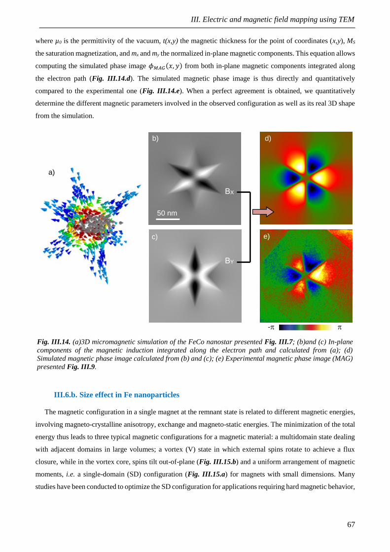
67
III. Electric and magnetic field mapping using TEM
where µ0 is the permittivity of the vacuum, t(x,y) the magnetic thickness for the point of coordinates (x,y), MS
the saturation magnetization, and mx and my the normalized in-plane magnetic components. This equation allows
computing the simulated phase image 𝜙𝑀𝐴𝐺(𝑥, 𝑦) from both in-plane magnetic components integrated along
the electron path (Fig. III.14.d). The simulated magnetic phase image is thus directly and quantitatively
compared to the experimental one (Fig. III.14.e). When a perfect agreement is obtained, we quantitatively
determine the different magnetic parameters involved in the observed configuration as well as its real 3D shape
from the simulation.
III.6.b. Size effect in Fe nanoparticles
The magnetic configuration in a single magnet at the remnant state is related to different magnetic energies,
involving magneto-crystalline anisotropy, exchange and magneto-static energies. The minimization of the total
energy thus leads to three typical magnetic configurations for a magnetic material: a multidomain state dealing
with adjacent domains in large volumes; a vortex (V) state in which external spins rotate to achieve a flux
closure, while in the vortex core, spins tilt out-of-plane (Fig. III.15.b) and a uniform arrangement of magnetic
moments, i.e. a single-domain (SD) configuration (Fig. III.15.a) for magnets with small dimensions. Many
studies have been conducted to optimize the SD configuration for applications requiring hard magnetic behavior,
b) d)
e)
BX
BY
50 nm
c)
a)
-
Fig. III.14. (a)3D micromagnetic simulation of the FeCo nanostar presented Fig. III.7; (b)and (c) In-plane
components of the magnetic induction integrated along the electron path and calculated from (a); (d)
Simulated magnetic phase image calculated from (b) and (c); (e) Experimental magnetic phase image (MAG)
presented Fig. III.9.

68
III. Electric and magnetic field mapping using TEM
such as hard disk drives126,210 or permanent magnets211,212,
while vortex state is sought in biological applications such
as hyperthermia or drug delivery121 to minimize the stray
field around the particle and thus prevent magnetic
aggregation213, or in spin-torque vortex-oscillator devices
for microwave signal-processing applications.214 In these
contexts, studying at room temperature the single-domain
limit separating SD and V states is particularly interesting.
The determination of this SD limit in a single nanoparticle
is predicted to be in the order of several exchange lengths,
i.e. from 15 to 25 nm depending on the material.215,216
Though spin configurations were experimentally
determined in different nanomagnets, no result has been
reported on the experimental determination of the critical
size, even for nano-objects with the simplest geometries.
This is mainly due to the limited sensitivity and resolution
of existing experimental techniques, which do not allow
studying isolated nanomagnets of size close to the expected transition. In addition, the investigation of the SD/V
transition required peculiar sample preparation. Isolated nano-objects are mandatory to prevent any influence
of dipolar interactions on the magnetic configuration of the object under study. Moreover, defect-free
nanomagnets with controlled and reproducible magnetic properties should be sought to allow accurate modeling
and comparison with experimental investigations.
In this context, I used EH to map the remnant magnetic configurations of Fe nanocubes [A15, A35, A63].
These particles were synthesized by L.-M. Lacroix and A. Meffre (LPCNO-INSA) using the organometallic
method, which results in quasi-monodispersed cubes with well-defined size. These Fe nanocubes, whose size
can be tuned at the frontier between the monodomain and the vortex states, are therefore considered as model
nano-objects to study the influence of shape and size on magnetic properties. Statistical measurements of the
size by conventional TEM observations revealed a dispersion of about 10% giving a thickness to length ratio of
1±0.1. High-resolution TEM experiments indicate that the Fe nanocubes are single crystalline and present body-
centered cubic (bcc) structure with {100} type facets (Fig. III.15.d). A thin layer of iron oxide (most likely
Fe3O4) of 1 or 2 nm surrounds each particle. This oxide appears when transferring the sample into the TEM.
Their simple shape favors the control of the nano-object orientation once deposited at the surface. Indeed, in
contrast to spheres217, cubes can lay on a surface along one of their faces, orienting their crystallographic
structure for TEM observations and their magnetization for magnetic imaging.
In a first work in 2008 done in collaboration with the LPCNO laboratory, we studied the magnetic
configurations of individual and interacting single crystalline 30 nm Fe nanocubes [A15]. EH experiments were
performed using the FEI Tecnai F20 microscope with a limited signal-to-noise ratio and a spatial resolution of
a few nanometers. Nevertheless, we evidenced a vortex state on isolated cubes which fulfilled the largest
Fig. III.15. Schematic 2D view of (a) a single-
domain and (b) a vortex spin arrangement in a
square magnetic element. (c) Transmission
electron microscopy (TEM) micrograph of Fe
nanocubes. (d) High resolution TEM
micrograph of a single Fe nanocube.

69
III. Electric and magnetic field mapping using TEM
cylinder, fitting perfectly the central part of the cube. The magnetization continuously curls around the [001]
axis with components in the (001) plane and turns progressively in the [001] direction parallel to the electron
beam when approaching its core. This vortex configuration, referred on as <001> vortex (V<001>) in the
following, was simulated by micromagnetic calculations (T. Blon, LPCNO-INSA) where the 3D nanocube
shapes and sizes introduced for the calculations were deduced from the 2D TEM images. The simulation fits
well with the EH results and confirms both the appearance of the vortex and the flux closure around the [001]
edges. Similar EH experiments and simulations were conducted on four cubes in a square arrangement. In that
case, the magnetic flux over the four cubes exhibits an axial symmetry, the centre of which is located in the
middle of the square. Here no vortex appears in that four cubes arrangement, i.e. the magnetization is only
curling around the middle of the square without any out-of-plane component. We have also shown results
combining EH and micromagnetic simulations for other configurations (2 and 4 cubes aligned). Our study
demonstrated that the magnetic configuration of Fe nanocubes strongly depends on their arrangement and
allowed us to understand the magnetic configuration of isolated nanocubes and magnetic interactions between
them.
All observations done in 2008 using the Tecnai F20 microscope on isolated Fe nanocubes showed a vortex
configuration and did not permit to study of the SD/V transition due to its limited spatial resolution of a few
nanometers in Lorentz mode. Indeed, micromagnetic calculations predict a SD/V transition for a cube size about
25 nm. In addition, a 25nm Fe nanocube has a magnetic volume half less than a 30 nm nanocube. We therefore
needed a better sensitivity, but at the expense of the spatial resolution.
In 2012, the new Hitachi H3300C microscope (I2TEM) dedicated to interferometric studies with a spatial
resolution of 0.5nm in Lorentz mode and increased phase shift sensitivity thanks to the cold field emission gun
has been installed. We resumed the study of the SD/V transition focalized our attention on 25nm Fe nanocubes
[A63]. After evaluating their squareness distribution, several iron nanocubes have then been investigated by EH
to observe the most probable magnetic configurations. The spatial resolution of phase images reached 1 nm.
Surprisingly three different configurations have been obtained. A V<001> configuration has still been observed
on a 27×26×(27±5) nm3 nanocube with a very good quantitative agreement between simulated and experimental
phase shift maps (Fig. III.16).
We then studied a slightly smaller cube with dimensions of 24×26×(25±4) nm3 (Fig. III.17). The flux lines
are fairly aligned within the cube and tend to curl outside in order to close the induction flux. Perfect agreement
between experimental and simulated magnetic phase images confirmed that SD is experimentally observed. A
closer look at the vicinity of the edges revealed that the magnetization goes out due to the inhomogeneity of the
stray field and makes this SD state usually referred as flower state.215,218–220 For an intermediate nanocube of
25×27×(26±4) nm3, the extracted magnetic phase image presented a complex pattern which cannot be directly
interpreted (Fig. III.18)

70
III. Electric and magnetic field mapping using TEM
The micromagnetic simulation of a cube of similar dimension obtained after relaxation of a randomly spin
orientation leads to a complex spin arrangement (Fig. III.18.c): its projection along the cube diagonal revealed
that spins curl around <111> direction. This complex configuration is therefore a vortex, the core axis of which
is aligned along the diagonal of the cubes, referred hereafter as vortex <111> (<111> vortex). A quantitative
comparison of linear profiles evidenced a good agreement between experimental and simulated profiles.
These experimental configurations and the size at which they were observed have been compared with
theoretical results. No intermediate state was predicted in previous numerical studies.215,218,219 However the
present data on single-crystalline Fe nanocubes of cubic anisotropy demonstrated that the three SD, <111> and
<001> vortices are stable configurations. In order to address more precisely the stability of each configuration,
we performed additional micromagnetic simulations. We computed the resulting energies for which the initial
spin configuration, uniform SD or V<001>, was imposed as the function of the nanocube sizes (Blue and red
curves on Fig. III.19).
Fig. III.16. Magnetic EH vs. micromagnetic
simulations of an isolated Fe nanocube of
27×26×(27±5) nm3. (a) Experimental hologram and (b)
resulting magnetic phase shift map. (c) Cosine of the
experimental phase image corresponding to the
magnetic induction flux lines. The inset color wheel
indicates the direction of the magnetic induction. (d)
Simulated magnetic phase shift map calculated from
micromagnetic simulations (dashed box indicates the
cube position). (e) 3D view of the magnetization
obtained at the equilibrium state for a simulated cube
of 29.53 nm3 (27.53 nm3 Fe core and a 1nm Fe3O4 shell).
(f) Comparison of experimental and simulated profiles
along the arrows indicated in (b) and (d).

71
III. Electric and magnetic field mapping using TEM
The magnetic transition between SD and V<001> occurs at 27 nm. The SD configuration is favored for small
sizes as it minimizes the exchange energy at the expense of magneto-static energy which scales with the volume.
In contrast, V<001> minimizes the magneto-static energy but leads to an increase of the exchange energy due
to the spin disorientations between “vertical” spins in the core and “horizontal” spins at the cube periphery.
When the cube size is reduced, the angle between neighboring spins from the center to the periphery become
larger and increase the exchange cost. In a second step, we introduced a random spin configuration and
computed the energy corresponding to a stable configuration after relaxation of the spins. Below 25 nm (above
29.5 nm), stable SD (V<001>) configurations were observed (blue circles and red squares respectively in Fig.
Fig. III.17. (a) Electron hologram of a
24×26×(25±4) nm3 Fe nanocube and (b)
corresponding magnetic phase shift map with 78
mrad isophase contours (as for (e)). (c) Cosines of
the experimental phase corresponding to the
magnetic induction flux lines. (d) Magnetic phase
shift map calculated from micromagnetic
simulations. (e) 3D view of the calculated
magnetization obtained at the equilibrium state for
a simulated cube of a 24×26×24 nm3 Fe nanocube
(22×24×22 nm3 Fe core surrounded with a 1 nm
Fe3O4 shell). (f) Comparison of experimental and
simulated profiles along the arrows indicated in (b)
and (d) (the vertical dashed lines indicate the cube
position).
Fig. III.18. (a) Hologram and (b) corresponding
magnetic phase shift map of a 25×27×(26±4) nm3 Fe
nanocube with 62 mrad isophase contours. (c) 3D
view of the simulated magnetization in a perfect Fe
nanocube of 263 nm3 (243 nm3 Fe core with a 1 nm
Fe3O4 shell) starting from an initial random
distribution of moments. (d) Projection of (c) along
the [11-1] direction of the cube illustrating a vortex
configuration with a core-axis parallel to the <111>
direction. (e) Calculated magnetic phase shift map
with same isophase contours as (b) obtained from the
simulation of a 263 nm3 cube. (f) Comparison of
experimental and simulated profiles along the arrows
indicated in (b) and (c).

72
III. Electric and magnetic field mapping using TEM
III.19). For intermediate sizes, between 25.5 and 29 nm, simulations evidenced <111> vortex as the most stable
configuration, the four equivalent directions [111], [111], [111] and [111] leading to similar energies. In this
size range where they are observed experimentally, V<111> have lower energy than SD and V<001>
configurations: the core axis aligned along a <111> direction permits to accommodate l the spin disorientation
along the nanocube diagonal between the vortex core and its periphery. Thus the V<111> allows balancing
exchange and magneto-static interactions at the expense of the magnetocrystalline energy which remains quite
low in Fe. We thus evidenced SD, <111> and <001> vortex states for cubes of roughly 25, 26 and 27 nm size
respectively, confirming the sharp but sequential transition between these three configurations when increasing
the nanocube size within a 3 nm window, demonstrating the key importance of nanometric size control of
magnetic nanoparticles.
To finish, an additional study has been conducted in collaboration with L.-M. Lacroix and T. Blon (LPCNO-
INSA) on 30nm size Fe nanocubes incorporating voids thanks to a fine-tuning of the growth environment and
the use of appropriate aliphatic surfactants [A35]. We showed that the presence of internal defects embedded
within cubes stabilizes vortex magnetic states within nanoparticle interacting assemblies. We thus provided
experimental proof for the potential interest of metallic porous cubes as stable vortices structures
III.6.c. The world of nanowires
Magnetic nanowires (NWs) are probably the nanosystems I most studied by EH. They are of great interest
due to their potential in the field of 3D magnetism and spintronics221–225 and became a very important topic in
magnetism both for theoretical and technological issues. Indeed, the understanding and observation of magnetic
configurations in 3D nanostructures became a major topic in nanomagnetism opening some new paths for
magnetic sensors, high-density data storage or magnetic domain wall based devices224 as Racetrack memory
concepts.225 In particular, there is an increasing interest for searching novel magnetic nano-objects allowing the
control of individual magnetic domain walls (DWs) motion.
One-dimensional (1D) nanostructures such as ferromagnetic self-standing nanowires (NWs) or patterned in
a planar shape are used to achieve a precise DW manipulation either by the application of magnetic fields or by
the injection of electric current. Magnetic nanocylinders are expected to show configurations reflecting the
Fig. III.19. Calculated magnetic energy of
ferromagnetic iron nanocubes (including a
1nm Fe3O4 shell) as a function of the total cube
size (range 15-40 nm). The energies were
calculated once the SD or V configurations
were reached. Comparison between random
(dots) and frozen SD (blue line) or Vortex
<001> (red line) initial states is reported.

73
III. Electric and magnetic field mapping using TEM
competition between dipolar and exchange energy. Their cylindrical symmetry prevents any change in the
demagnetizing energy as the spins rotate during DW propagation226,227 and should lead to a suppression of the
Walker breakdown228–230 encountered in nanostripes. A nice review of the current knowledge about the
synthesis, magnetic properties, and applications of magnetic cylindrical nanowires and nanotubes has been
recently published.231
However, the achievement of a controlled and reproducible DW handling requires a preliminary exhaustive
study focused on understanding how the remnant local spin configuration is distributed in individual and isolate
NWs, free of magnetic interaction among neighboring nanowires. While magnetic DWs have been almost
exclusively studied experimentally in nanostripes, I noticed that most of the research on nanocylinders has been
carried out by means of micromagnetic calculations, and very rarely correlated to experimental investigations.
Imaging and understanding the fine structure of the DW in nanocylinders was thus important to make these
systems an interesting alternative to the usual flat nanostripes produced by lithography.
Different methods have been used for mapping their magnetic configuration as magnetic force microscopy
(MFM), magneto-optic Kerr effect (MOKE), scanning electron microscopy with polarization analyzer
(SEMPA) or X-ray magnetic circular dichroism (XMCD-PEEM).231 These methods are complementary with
some advantages compared to EH. But they are in general sensitive to surface magnetization or stray field and
present a limited spatial resolution of few tens of nanometers. In contrast, EH offers quantitative information
on the internal magnetic structure with a spatial resolution down to 1 nm but with an integrated signal along the
electron path.
Through different collaborations, I have conducted studies for determining the remnant magnetic
configurations at the nanoscale in different types of cylindrical NWs: pure Ni nanowires for investigating the
domain wall structure [A38], FeCoCu diameter modulated for understanding the origin of bright and dark
contrasts observed in MFM images [A70] or multilayered Co-Cu NWs for analyzing their multiple magnetic
states [A66, A84, A85]. All these NWs have been grown using electrodeposition method which is one of the
most used techniques due to its ability to obtain nanowires with different sizes, shapes and composition in a
relatively easy and inexpensive way. Another common point between these different studies is the combination
of different electron microscopy techniques and micromagnetic simulations for a deeper understanding of the
magnetic states. We thus used EH to study the remnant magnetic states and the structural parameters of different
NWs with a high spatial resolution. Complementary structural and chemical properties were in some cases
determined by conventional and high-resolution electron microscopy, Energy Filtered Transmission Electron
Microscopy (EFTEM) and Electron Energy Loss Spectroscopy (EELS). The comparison of experimental
magnetic phase images with simulated phase images obtained by 3D micromagnetic calculations including the
geometrical parameters extracted from TEM experiments allowed an enhanced analysis of the remnant magnetic
configurations and the determination of the involved magnetic parameters such as the magnetization value, the
exchange constant or the magnétocristalline anisotropy.
I will not detail in the following the study on the magnetic configuration of isolated diameter modulated
FeCoCu nanowire [A70]. Only a summary of the studies I performed on pure Ni NWs and multilayered Co-Cu

74
III. Electric and magnetic field mapping using TEM
NWs will be presented [A38, A66, A84, A85]. I would also like to point out that I have participated to other
works on different types of 1D systems using EH such as cobalt nanostructures grown by Focused Electron
Beam Induced deposition (FEBID) techniques with ultra-small diameter (lateral size below 30 nm) [A30] or
larger diameter for quantitative 3D reconstruction of the magnetic induction and electrostatic potential [A62],
single-crystal Ni nanowires of 20 nm of diameter produced via a metal–organic precursor decomposition
synthesis in solution [A78].
III.6.c.1. Structure of a magnetic wall in a Ni nanowire
As explained previously, the DW manipulation in cylindrical NWs requires a detailed description of their
remnant magnetic state as a function of their structural properties and geometry. Indeed, magnetic nanocylinders
are expected to show a magnetic transition from vortex to transverse wall as the diameter is reduced.232,233 In
collaboration with N. Biziere (CEMES), I studied this transition on pure Ni nanocylinders with diameters around
80 nm ±25 nm [A38]. Conventional and high-resolution TEM demonstrated the polycrystalline structure of the
wire with randomly oriented grains, leading to a random distribution of the magnetocrystalline anisotropy and
grain sizes roughly equal to the wire diameter. Before imaging at the remanence, a 2 T magnetic field was
applied perpendicularly to the nanowire axis (z-axis parallel to the electron path) using the electromagnetic
objective lens of the microscope to favor transverse walls in nanowires of smallest diameter.
Fig. III.20.b and e display the experimental magnetic phase images induced by DWs appearing in two
nanocylinders of 55 and 85 nm diameter. Magnetic domain walls are evidenced by the stray field leaking outside
the wire in each side of the DWs. Inside the wire, the magnetic flux at the DW position is found to be asymmetric
Fig. III.20. Transverse DW and hybrid magnetic state in 55 and 85 nm nanocylinders. (a and d) Amplitude
image of 55 and 85 nm nanocylinders, respectively; (b and e) Experimental magnetic phase shift and
corresponding induction field lines; (c and f) Magnetic phase shift and corresponding induction field lines
calculated from micromagnetic simulation. The dashed lines are a guide for the eye to position the wires. The
arrows on the scheme represent a simplified view of the magnetization within the wire.

75
III. Electric and magnetic field mapping using TEM
as compared to the uniform case. Two different DW structures were found from two wires of different diameters.
For the smallest one (Fig. III.20.b), field lines are symmetric with respect to both the x and y-axis of the image
plane, and no magnetic induction is observed at the very center of the DW indicating that the magnetization at
this location is parallel to the electron beam path (z-axis). This is the magnetic configuration expected for a pure
transverse wall with the spins pointing in the direction of the saturation field. For the larger diameter wire (Fig.
III.20.e), field lines are symmetric with respect to a plane tilted at about 45° from the y axis. Such a magnetic
DW configuration does not correspond to a vortex state for which the magnetic flux should be confined within
the wire, with a round shape and without stray field.
Micromagnetic simulations have been performed for both studied NWs. For the 55 nm diameter wire,
calculations indicated a head to head transverse wall. The corresponding calculated phase shift is reported in
Fig. III.20.c. The qualitative and quantitative agreements between simulation and experiment clearly proved
the appearance of a transverse DW. Micromagnetic simulation showed a more complex head-to-head DW in
the 85 nm diameter wire with the appearance of a “pseudo transverse wall”. The presence of such a “pseudo”
transverse wall implies that the cores of the vortices are not centered along the wire axis inducing clockwise
and anticlockwise rotation of the vortices on each side of it. As for the 55 nm diameter case, the phase shift
calculated from this magnetic state (Fig. III.20.f) is in perfect agreement with the experimental result (Fig.
III.20.e). As the cores of the vortices are not aligned with the y-axis, the resulting uncompensated flux closure
induces the appearance of a stray field as experimentally observed. This result was the first evidence of a
magnetic transition in a cylindrical nanostructure from a pure transverse wall to a hybrid magnetic configuration
whose fine structure has been clearly elucidated. We observed that such hybrid state strongly depends on the
magnetic history of the nanostructure: saturating the magnetization perpendicular to the wire axis did not lead
systematically to the pinning of a DW. As already stated, shape anisotropy tends to align all of the spins in the
direction of the NW axis to stabilize a uniform magnetic state. A DW can nucleate but moves and collapses at
the NW edge leading to a uniform magnetic state. However, the polycrystalline structure plays a major role in
the DW pinning, most probably on grain boundaries.
During this study, we acquired magnetic phase images on the edges of the Ni NWs for analyzing the leak
field emanating from the tip. Due to the cylindrical symmetry of the NW and its magnetic field, these images
have been used in a novel method based on the inverse Abel transform for quantitative determination of the 3D
electromagnetic fields in and around 1D nanostructures using a single phase image, thereby eliminating the
cumbersome acquisition of tomographic data (Fig. III.21) [A67]. This last work was done in collaboration with
A. Masseboeuf (CEMES) and C.D. Phatak (Argonne National Laboratory, US).

76
III. Electric and magnetic field mapping using TEM
III.6.c.2. Structural and magnetic interplay in CoCu multilayered nanowires
The Co-Cu multilayered NWs are an important topic in my activities as one of my PhD students (D. Reyes,
2013-2106) studied their magnetic configurations using EH in collaboration with B. Warot-Fonrose and N.
Biziere (CEMES) [A66]. We still continue to work on these NWs with new submitted articles on the 3D
reconstruction of the internal magnetic states by Vector Field Electron Tomography (VFET) [A84] in
collaboration with D. Wolf and A. Lubk from the Institute for Solid State Research at Dresden (Germany), and
a detailed comparison between EH experiments and micromagnetic analysis of all the possible configurations
as a function of geometrical parameters [A85].
Despite the strong interest for the novel cylindrical nanostructures, multilayered systems with such geometry
have been poorly studied up to date while they present multiple advantages for many magnetic applications.
Besides the possibility to get a relatively high Giant Magneto-Resistance234 at room temperature, they are basic
blocks for synchronized spin torque nano-oscillators.235 They are also interesting for developing thermoelectric
applications236 or novel magnonics devices.237 In order to realize such applications, controlling the magnetic
states of the different magnetic layers is a crucial step. In particular, the interlayer dipolar coupling of these
multilayers complicates further the understanding of the magnetic state as metastable states in the individual
layers can be stabilized. Studying the stray field of Co/Cu nanowires, Beeli et al.238 observed that the remnant
states vary with both their diameter and the direction of the magnetic field applied before the observations.
Several magnetic configurations were confirmed, changing from parallel to antiparallel coupling between the
Co layers. The interlayer dipolar coupling is then a key point for a deeper knowledge of the interplay between
magnetic states and local properties in multilayers in order to control the properties of the potential devices.
Fig. III.21. (a) Electrostatic contribution to the phase shift of the nickel nanowire. (b) Magnetic
contribution to the phase shift. (c) By component calculated from the gradient of magnetic phase
shift, and (d) shows the By component in the x- y plane in the middle of the nanowire. The color
represents the strength of magnetic induction indicated by the color bar. (e) 3D vector plot of the
reconstructed magnetic induction from the nanowire. The vectors are colored according to the y
component of the induction indicated by the color bar (in units of T).

77
III. Electric and magnetic field mapping using TEM
We have thus performed a detailed study of the internal magnetic remnant states of Co/Cu multilayered
nanocylinders grown by electrodeposition in commercial polycarbonate membranes. Their diameters range
between 60 and 90 nm. In order to investigate the effect of the aspect ratio and dipolar coupling on the magnetic
states, four series of samples with different nominal Co and Cu thicknesses have been realized, namely Co25
nm/Cu15 nm, Co25 nm/Cu45 nm, Co50 nm/Cu50 nm and Co100 nm/Cu100 nm. Prior to the EH observations of the remnant
magnetic states, the NWs were saturated with a magnetic field of 1T produced by an external electromagnet. A
first observation was performed with a saturation field applied in a direction parallel to the NW axis before a
second observation on the same NWs after saturation perpendicular to the NW axis.
Co25 nm/Cu15 nm system was the first studied system and was used to develop our methodology combining
EH, structural and chemical TEM experiments with micromagnetic simulations on the same NW [A66]. Fig.
III.22.a shows a TEM image of a representative NW. Local chemical analysis performed by EELS and EFTEM
allowed to distinguish the nanodisks and showed a rotation of a few degrees with respect to the wire axis (Fig.
III.22.b). In addition, while Co impurities are barely visible in the Cu layers, a Cu amount of about 15% has
been measured in the Co part. This result, already reported in other works239–241 dealing with electrodeposition
process, is explained by the single bath method: as the deposition potential is lower for Co (-1 V) than for the
Cu (-0.3 V), a small amount of Cu is co-deposited during the Co deposition.
We recovered the different magnetic remnant
configurations by electron phase shift
reconstruction with a 2 nm spatial resolution.
Through statistical analysis performed on many
NWs, three different states have clearly been
identified as a function of the direction of the
saturation field and structural properties: an
antiparallel magnetic coupling between adjacent
Co nanodisks presenting in-plane magnetization,
coupled vortices or monodomain configurations.
We found that, when the saturation field was
applied perpendicular to the NW axis, about 70%
of the layers showed the antiparallel coupling
(Fig. III.22.d). For a saturation field applied
parallel to the NW axis, we observed a change of
the magnetic configuration resulting in coupled
vortices for only about 20% of the Co layers (Fig.
III.22.c). Finally, in some rare cases (10%),
uniform alignment of the magnetization in all
layers in the direction of the NW axis has been
detected.
Fig. III.22. (a) TEM image of a Co25 nm/Cu15 nm nanowire.
b) EFTEM image of the same area to distinguish the
copper (blue) and cobalt (red) layers. c) Magnetic phase
shift map obtained after the application of the parallel
saturation field with respect to the wire axis. d) Magnetic
phase shift map obtained after the application of the
saturation field perpendicularly to the wire axis.
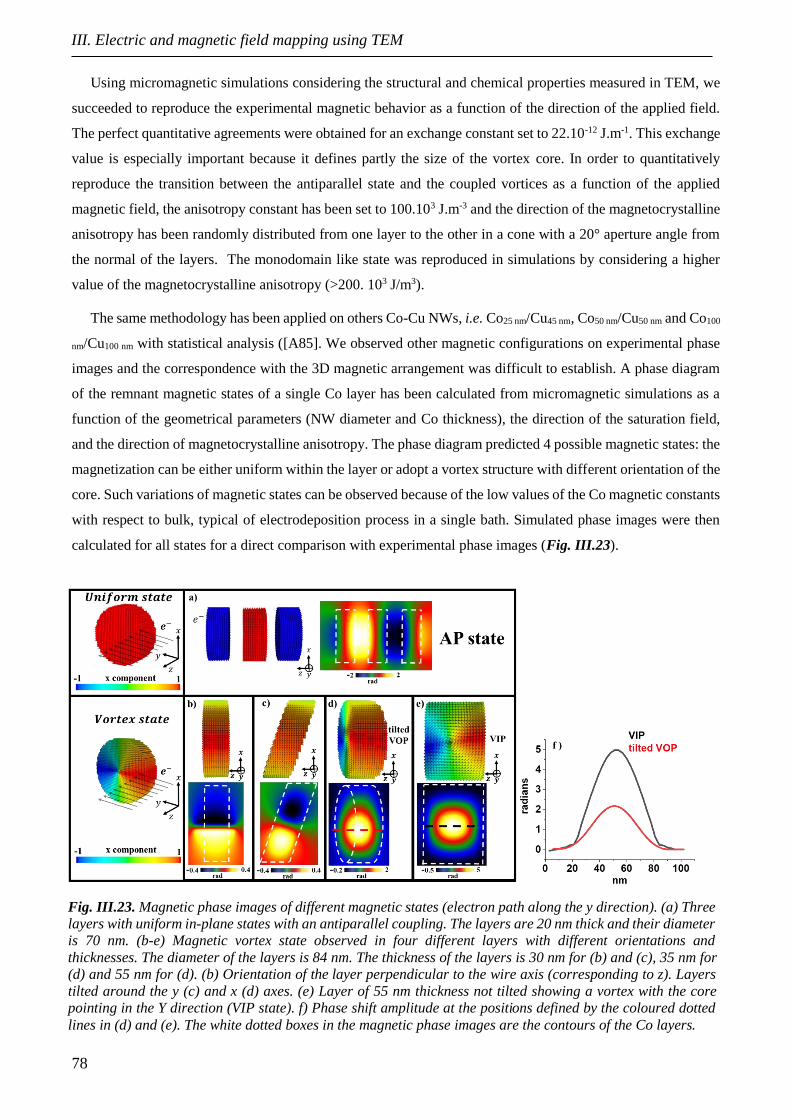
78
III. Electric and magnetic field mapping using TEM
Using micromagnetic simulations considering the structural and chemical properties measured in TEM, we
succeeded to reproduce the experimental magnetic behavior as a function of the direction of the applied field.
The perfect quantitative agreements were obtained for an exchange constant set to 22.10-12 J.m-1. This exchange
value is especially important because it defines partly the size of the vortex core. In order to quantitatively
reproduce the transition between the antiparallel state and the coupled vortices as a function of the applied
magnetic field, the anisotropy constant has been set to 100.103 J.m-3 and the direction of the magnetocrystalline
anisotropy has been randomly distributed from one layer to the other in a cone with a 20° aperture angle from
the normal of the layers. The monodomain like state was reproduced in simulations by considering a higher
value of the magnetocrystalline anisotropy (>200. 103 J/m3).
The same methodology has been applied on others Co-Cu NWs, i.e. Co25 nm/Cu45 nm, Co50 nm/Cu50 nm and Co100
nm/Cu100 nm with statistical analysis ([A85]. We observed other magnetic configurations on experimental phase
images and the correspondence with the 3D magnetic arrangement was difficult to establish. A phase diagram
of the remnant magnetic states of a single Co layer has been calculated from micromagnetic simulations as a
function of the geometrical parameters (NW diameter and Co thickness), the direction of the saturation field,
and the direction of magnetocrystalline anisotropy. The phase diagram predicted 4 possible magnetic states: the
magnetization can be either uniform within the layer or adopt a vortex structure with different orientation of the
core. Such variations of magnetic states can be observed because of the low values of the Co magnetic constants
with respect to bulk, typical of electrodeposition process in a single bath. Simulated phase images were then
calculated for all states for a direct comparison with experimental phase images (Fig. III.23).
Fig. III.23. Magnetic phase images of different magnetic states (electron path along the y direction). (a) Three
layers with uniform in-plane states with an antiparallel coupling. The layers are 20 nm thick and their diameter
is 70 nm. (b-e) Magnetic vortex state observed in four different layers with different orientations and
thicknesses. The diameter of the layers is 84 nm. The thickness of the layers is 30 nm for (b) and (c), 35 nm for
(d) and 55 nm for (d). (b) Orientation of the layer perpendicular to the wire axis (corresponding to z). Layers
tilted around the y (c) and x (d) axes. (e) Layer of 55 nm thickness not tilted showing a vortex with the core
pointing in the Y direction (VIP state). f) Phase shift amplitude at the positions defined by the coloured dotted
lines in (d) and (e). The white dotted boxes in the magnetic phase images are the contours of the Co layers.

79
III. Electric and magnetic field mapping using TEM
All these states have been observed using EH, demonstrating that information on the magnetocrystalline
anisotropy, and then potentially on the local structure of the Co layers, can be recovered by applying a saturation
magnetic field in different directions. Our observations proved that the amplitude of the magnetocrystalline
anisotropy decreases when increasing the thickness of the Co layer, in agreement with an averaging due to the
random distribution of the crystallographic grains. However, the interlayer dipolar coupling can strongly modify
the remnant state of a system as compared to the case of a single layer. For instance, an antiparallel coupling of
uniform states in very thin Co layers is favoured, even for Cu thickness up to 40 nm. But in a very thick layer
with an aspect ratio close to 1, the dipolar coupling stabilizes the magnetization along the direction of the NW
axis.
To conclude, while electrodeposited nanocylinders are a nice playground for fundamental studies because
of the wide variety of states, their use for potential applications requires further control of the structural
properties of the layers. As an example, we often observed different configurations within the same nanowire
due to the local variation of geometry and/or chemical composition. This might be a problem for applications
such as spin torque oscillators. Indeed, the geometry of the layers must be the same for all layers in order to
ensure the same resonance frequency, precession amplitude and to allow phase locking between layers.
A last study has been conducted on the Co25 nm/Cu15 nm system using the holographic VFET method in
collaboration with D. Wolf ad A. Lubk (Institute for Solid State Research, Dresden) [A84]. It consists in
combining EH and tomography experiments for reconstructing the 3D magnetic induction and the 3D chemical
composition with a high spatial resolution. Dual-axis tilt series of holograms were acquired within a tilt range
of 280° before holographic phase reconstruction, precise image alignment, separation of electric and magnetic
Fig. III.24. 3D reconstruction of a multi-layered Co25 nm/Cu15 nm nanowire. (a) The volume rendering of the
mean inner potential of the nanowire display Co in red and Cu in bluish/white. The arrow plots represent the
field line of magnetic induction sliced through 8 disks, where the direction of the normal component of the
induction is color-coded in black and yellow. (b) Slices through the Co disks as indicated in (a): Co disks 2 and
7 show in-plane magnetization, 1,3,5,6 counter-clock-wise, and 4,8 clock-wise vortex magnetization.

80
III. Electric and magnetic field mapping using TEM
phase shift and tomographic reconstruction of all three induction components. The results obtained on the Co25
nm/Cu15 nm multilayers painted a complex picture of the 3D magnetization behavior, as the coexistence of vortex
and in-plane magnetized states (Fig. III.24). The findings confirm the 2D analysis detailed previously [A66].
However, this allowed to set up a micromagnetic model including the exact geometry of the Co nanodisks that
matches the experimental induction field tomogram from which magnetic parameters of individual layers can
be derived more precisely. Avoiding problems of geometrical uncertainties as well as providing additional data
terms of the 3D field distribution for optimizing micromagnetic simulation is a great advance for a precise
analysis of the magnetic properties of nanostructures. I continue to strongly collaborate with D. Wolf and A.
Lubk on this topic.
III.6.c.3. Prospects for EH studies on nanowire
My activity on cylindrical magnetic NWs studied by EH is currently going on with a Ph.D. student (I.-M.
Andersen, 2017-2020) in collaboration with E. Snoeck (CEMES), A. Masseboeuf (CEMES), the Instituto de
Ciencia de Materiales de Madrid and the Institute for Solid State Research at Dresden.
We are working on CoNi cylindrical NWs displaying grains of both fcc and hcp crystal phase, where the hcp
phase has the c-axis oriented perpendicular to the nanowire axis [A87]. The magnetic configurations in various
Co-based cylindrical nanowires have previously been studied in several publications242–244, which have revealed
a strong influence of the NW’s structural properties, depending thus on their fabrication process245,246. For
instance, it has been shown that monocrystalline Co hcp phase can be obtained in pure Co NWs with the c-axis
perpendicular to the NW axis. The corresponding uniaxial magnetocrystalline anisotropy is then strong enough
to challenge the large shape anisotropy of NWs245,247,248. In CoNi-alloy NWs, the amount of Ni content can
modify the crystallographic phase: while Co NWs with a low Ni content keep a hcp phase with a strong magnetic
anisotropy and a resulting magnetic induction perpendicular to the NW axis, high Ni content generally leads to
fcc crystal structure with a lower magnetocrystalline anisotropy249,250 and a parallel magnetic induction. Tuning
the CoxNi1-x content then allows for adjusting the magnetic easy axis orientation from parallel to perpendicular
relative to the nanowire axis245. 17,19 and therefore make the CoNi-alloy NWs very interesting as potential
building blocks for future devices.
However, previous publications have evidenced the coexistence of fcc and hcp crystal phases in single CoNi
alloy NWs249,251–253, but there has been little or no report on how they mix and affect the magnetic configuration
of the NW. Only statistical overviews of the structural and chemical information has been reported as the crystal
phase and composition in NWs are often determined by techniques like x-ray diffraction (XRD) and energy
dispersive x-ray microanalysis (EDX) on assemblies or arrays of NWs245,246. To gain control over the
magnetization states and reversal mechanisms, a precise analysis of the local structure of a single nanowire,
combined with its magnetic configuration, is required. A quantitative study of both the structure and the
magnetic properties obtained on the same area and at the nanoscale demands versatile and advanced techniques
in combination with sufficient spatial resolution and sensitivity. In the PhD topic of I.-M. Andersen, we combine
EH with classical TEM, Scanning TEM (STEM)-EELS and ASTAR measurements, a diffraction spot

81
III. Electric and magnetic field mapping using TEM
recognition technique based in the TEM, to quantitatively observe the magnetic induction of cylindrical Co85Ni15
nanowires, i.e. NWs with a low Ni content, prepared by electrodeposition, in relation to their local
crystallographic structure and chemical composition. In addition, micromagnetic OOMMF simulations are
carried out for a deeper analysis of the experimental results. This correlative study of TEM methods combined
to micromagnetic simulations allowed us to unambiguously determine the main parameters involved the
magnetic configuration.
Fig. III.25. (a) BF-TEM image and (b) over-focused Lorentz image of sample NW. (c) unwrapped magnetic
phase shift image of stippled region marked in (b), and (d) magnetic flux lines obtained from the cosine of (c)
with amplification factor 4.
EH revealed an inhomogeneous magnetic configuration within a single nanowire representative for the whole
sample. This complex magnetic configuration consists in curling states parallel to nanowire axis, a chain of
antiparallel domains oriented perpendicular to the nanowire axis, and a magnetic transition state between these
two (Fig. III.25). The experimental results have been compared to micromagnetic simulations, revealing a chain
of perpendicularly oriented vortex domain walls separating the antiparallel domains. Correlated local changes
in composition and crystal structure have been highlighted as the origin of the different magnetic configurations
(Fig. III.26). The chain of vortex domain walls oriented perpendicular to the nanowire axis is the result of the
hcp phase whose easy magnetic c-axis is oriented 80 relative to the NW axis and counterbalances the shape
anisotropy. A curling state with a magnetic induction component oriented along the NW axis is appearing in fcc
phase where the easy axis and shape anisotropy act in the same way. A transition region between these two
configurations is observed at the fcc/hcp grain boundary running almost parallel to the NW axis.

82
III. Electric and magnetic field mapping using TEM
Fig. III.26. Experimental results of structural analysis of nanowire region. (a) Pole figure showing [0001] hcp
crystal grain orientations from the region highlighted by blue square in (c). (b) virtual bright field image of
scanned nanowire area. (c) virtual crystal phase map of region in (b), where black pixels represent highest
match for fcc phase, and colored pixels for hcp. The pixel colors correspond to [0001] orientations with the
same color as in (a). (d) superimposed magnetic phase shift image and virtual crystal phase map of the same
nanowire region (marked by yellow square in (c)).
This study demonstrates the strong correlations between crystal structure and composition, and consequence
on the magnetic configurations in CoNi NWs. The effect of local crystalline changes is found to drastically
change the magnetic configuration in the NW, and can therefore not be neglected when attempting to explain
and analyze the magnetic structure. A correlative microscopy investigation has a great advantage in such a
study, as it offers magnetic, structural and spectroscopic analysis of the exact same area, since the same sample
can be inspected by different microscopic techniques. We are currently conducting a deeper study of this
complex magnetic configuration using the holographic VFET method in collaboration with D. Wolf ad A. Lubk
(Institute for Solid State Research, Dresden). It will allow obtaining a direct 3D visualization of the chain of
vortex domain walls and the curling magnetic state of these NWs.
Another part of the Ph.D. work is to develop in situ/operando EH experiment for applying an electrical
current across the magnetic NW. The aim is to manipulate domain walls during the TEM observations. This
topic which requires advanced sample preparation and dedicated setup for acquiring holograms is a part of my
project.
III.6.d. Inhomogeneous spatial distribution of magnetic transition in epitaxial thin layers
The control of a magnetic state by thermal or electrical activation is essential for the development of new
magnetic devices, for instance in heat or electrically-assisted magnetic recording or room-temperature memory
resistor.109,111,112 Compounds such as FeRh or MnAs, which undergoes a magnetic transition from a
ferromagnetic state to a state of zero magnetization close to room temperature are expected for such applications.
As detailed in section II.3.b, the FeRh alloy presents an unusual magnetic transition from a low temperature
antiferromagnetic (AFM) state to a high temperature ferromagnetic (FM) state close to 370K accompanied by
a 1% volume expansion.90–94 The transition takes place for a narrow composition range 0.48<x<0.56 and is only
obtained for the B2-ordered ’ crystal phase of Fe1-xRhx. MnAs presents a magnetostructural phase transition
from the ferromagnetic hexagonal phase (NiAs type symmetry, B81) to non-ferromagnetic (N-FM)
orthorhombic β phase (MnP type symmetry, B31) around 40°C. This N-FM is in general associated with a
paramagnetic state but an AFM state with a very slight antiparallel coupling has also been proposed. Most

83
III. Electric and magnetic field mapping using TEM
interestingly, the parameters of the transition are different in MnAs thin films grown on GaAs substrate
compared to bulk MnAs: the temperature range where and β domains coexist broadens and varies with the
film thickness, orientation and deposition conditions. The phase coexistence is explained by the constrained
lateral size and constant mean lattice spacing in the MnAs layer254,255: the thermal dilatation and crystalline
transformation give rise to an elastic strain that can be relaxed through the coexistence of and domains.
If both alloys present a first-order magnetic transition, the magnetic transition in MnAs is related to an
important structural change, and is thus described as a magnetostructural transition. For FeRh, the transition can
be associated to a pure magnetic transition due to the very slight change of the lattice parameter. In addition,
the FM domains in MnAs have a strong magnetocrystalline anisotropy along the [11-20] direction of the
hexagonal phase while the magnetocrystalline anisotropy is quite low for the cubic structure of FeRh in its FM
state. The investigation of the transition mechanisms has been proposed using many different methods studying
the transition from the corresponding magnetic states101,103,116,256–259 or, for MnAs, from a purely structural point
of view.255,256,260,261 Among other results, a persistence of a FM component has in general been reported at room
temperature or even below in thin FeRh films115,259,262 or at the interface between the film and the capping
layers.101,103 This persistent FM signal was attributed to chemical diffusion, surface segregation or misfit strain,
and often to a combination of these different effects. The role of surface or interface in the nucleation of the FM
domains at the onset of the transition was also analyzed experimentally.106,116,263,264 However, the mechanisms
involved in the transition for both alloys are still under debate.
Local magnetic techniques, such as magnetic force microscopy (MFM)258,265,266 and X-ray magnetic circular
dichroism photoemission electron microscopy (XMCD-PEEM)106,116,257,263,264,267,268 have therefore been
performed on both alloys. Viewed from the film surface plane, the FM α-MnAs and N-FM β-MnAs phases
coexist in a form of a self-aligned array of stripes between around 20 and 50°C255,261,269, and the width of α-
MnAs stripes is continuously tunable by varying the temperature.257,258,267 Concerning FeRh, few studies have
mapped the transition on thin films.106,263,270 All of them have reported co-existing FM and AFM domains on
the top surface and the subsequent expansion of the FM domains. At this point, it is important to notice that all
magnetic imaging methods used for mapping the magnetic transition are surface investigation techniques,
without visualization of the magnetic reorganization in volume, and mainly performed on a plane view
configuration. The knowledge of this plane view magnetic configuration is not sufficient to offer a full
understanding of the structural local transition mechanisms in thin films for future applications. The cross-
section in-depth information with quantitative values of the magnetization seemed mandatory to me for a deeper
analysis of the transition. In addition, a spatial resolution better than a few tens of nanometers was required to
observe the possible effects of surface and interface as well as inevitable defects on the transition. I consequently
chose to apply EH in cross-sectional view for quantifying the magnetization in the inner part of FeRh and MnAs
layers at the highest spatial resolution and as a function of the temperature [A74, A76].

84
III. Electric and magnetic field mapping using TEM
III.6.d.1. Investigation of a FeRh thin film
In collaboration with M.-J. Casanove (CEMES), a 50nm FeRh film was epitaxially grown on a MgO (001)
substrate by DC sputtering and in situ annealed. We first checked the presence of AFM/FM transition by
vibrating sample magnetometry (VSM). The cross-sectional lamella was then prepared by FIB to ensure a
uniform thickness crossed by the electron beam, and the FeRh layer was protected by ink and platinum layers
to avoid damages and charge accumulation during the thinning process. The growth axis is [001] and the layer
is observed along the FeRh [-110] axis ([100] for MgO). The final thickness of the lamella was measured at
90±5 nm after a low energy step to minimize irradiation damages and surface amorphization. For the EH
experiment, the sample temperature was first stabilized at +125°C to get the FeRh layer into the FM state before
applying an in situ magnetic field to saturate the specimen parallel to the [110] direction of FeRh. A first set of
holograms was acquired during a temperature decrease down to -120°C (cooling process) before recording a
second series of holograms during the heating process up to +125°C. All the holograms were acquired at the
remnant state on the same area after temperature stabilization to perform a static study of the transition [A76].
The spatial resolution of the extracted phase images is equal to 2.5nm.
The FM state clearly showed up on the magnetic phase image obtained at +125°C with the appearance of a
phase shift inside the FeRh layer (Fig. III.27.b). The phase shift profile parallel to the FeRh growth direction
averaged over the whole field of view presented a linear variation indicating that the induction was spread
homogeneously within the FeRh film (Fig. III.27.d). From the mean slope of the phase shift profile and the
width of the TEM lamella, I calculated a magnetization µOMx equal to 1.19±0.13 T (Eq. III.11 and III.12). This
Fig. III.27. Amplitude and magnetic phase images for the two extreme temperatures. (a) Amplitude image of
the studied area (630 nm x 190 nm). (b) Magnetic phase image obtained at +125°C. The FeRh layer is between
horizontal dashed lines at the right of the image. The white arrow and isophase lines parallel to the magnetic
induction lines into the FeRh layer have been added for clarity. (c) Magnetic phase image obtained at -120°C.
(d) Magnetic phase shift profiles along the y direction averaged over the x direction for the whole field of
view. The red and blue curves correspond to the profiles extracted at +125°C and -120°C respectively. Scale
bars represent 50 nm.

85
III. Electric and magnetic field mapping using TEM
value is in very good agreement with previous magnetization value obtained at the FM state.99,101,115 However
the magnetic phase image recorded at -120°C (Fig. III.27.c) showed a strong decrease of the total phase shift
corresponding to a residual magnetization parallel to the film equal to 0.28±0.13 T. This value appeared to be
higher than previously reported.103,271 We explained this apparent discrepancy taking into account the
amorphous layers on each side of the thin lamella creating during the lamella preparation process by FIB.
Indeed, the FM to AFM transition upon cooling, only present in the B2 phase, is impeded in these regions which
remain in the FM state. Assuming a minimum thickness of 5nm for each layer, these two damaged FM layers
correspond to more than 10% of the total width of the thin lamella crossed by the electron beam. The
magnetization of the AFM state limited to the B2 phase thickness (80nm) was therefore calculated equal to 0.166
T in reasonable agreement with values measured by VSM and other studies. This value would be lower for
thicker damaged layers with a magnetization of the AFM state approaching 0.
For a deeper local analysis of the AFM/FM transition, I studied the evolution of the temperature transition
along the growth direction using a rectangular window of 4nm width and elongated parallel to the interface with
the MgO substrate over 630 nm. The area enclosed by the window was shifted by 1 nm along the growth
direction and, for each position, a complete loop µ0M = f(T) was extracted. Fig. III.28 presents the evolution of
the AFM/FM transition from the bottom interface to the top surface. The first 3 nm close to both interfaces have
been excluded because of artefacts in the data processing. The main result is the evidence of the heterogeneity
of the transition: close to the interfaces, especially close to the top surface, the magnetic transition from the
AFM state to the FM state starts at much lower temperature and is spread over a wider range of temperature
Fig. III.28. Evolution of the AFM/FM transition along the growth direction. (a) Map of the magnetization
as a function the temperature and the position in the layer depth using the “Heating” temperature series.
The color scale corresponds to the magnitude of the magnetization and the transition temperature is
displayed by the white profile corresponding to magnetization of 0.75 T. (b) Amplitude image of the part
of the FeRh layer used for the calculation. (c) Profiles of the transition temperature TT and the transition
width T as a function of the position within the FeRh layer.

86
III. Electric and magnetic field mapping using TEM
than in the middle of the layer. The profiles of the transition temperature (TT) and the transition width (T) along
the growth direction have been extracted from the left part of Fig. III.28 and are shown in the right part. TT is
lower close to the interfaces than in the middle of the layer with a difference up to 50°C. The core of the layer
presents a 30 nm plateau with a mean value of TT slightly lower than 60°C. TT decreases towards the interfaces
down to 10°C over a width of 5 to 10 nm. By superimposing the transition width T and TT profiles as a function
of the position in the film, a clear match occurs: the lower TT, the wider the transition. Similar results are obtained
studying the “Cooling” or “Heating” series.
If the presence of interfaces is considered to favor the FM state114,115,263, the stress is also suspected to play a
role.99,103,264 In our case, the interdiffusion of the ink layer is most likely very limited and has no effect, as it was
deposited at room temperature and the maximum temperature the system reached is 125°C. Any structural
defects have been seen in the FeRh layer at the top surface compared to the inner part. A slight oxidation of the
FeRh would spread over less than 2nm and has not been observed. So even if we cannot exclude a slight effect
of stress, symmetry breaking seems to be the most likely responsible for the magnetic behavior changes.
Regarding the MgO/FeRh interface, a diffusion of Mg might have occurred and the presence of structural defects
such as misfit dislocations at this interface certainly promotes magnetic transition changes. These different
mechanisms are sufficient to explain the slight asymmetry of the TT and T profiles between both interfaces.
We observed also that the interface effects extend up to 15 nm, i.e. deeper into layer than previously assumed
in other studies. Both interfaces have thus a huge influence on the AFM/FM in the same way by reducing TT
and broadening the temperature range necessary for the transition. This result is of large importance since it
explains why various experimental measurements observe a decrease of the transition temperature with the
decrease of the layer thickness and predict the difficulty to obtain an AFM/FM transition in FeRh nanoparticles
of few nanometers diameter. In addition, interface effects have to be taken into account when FeRh layer is
integrated in a device and coupled with adjacent (magnetic) layer.109,111,112
The magnetic phase images corresponding to the main stages of the transition from low temperatures to high
temperatures are presented in Fig. III.29. The color scale is common to all images. The gradual increase of the
total phase shift with increasing temperature reflects the appearance of the FM state. The magnetic configuration
varies significantly from 45°C. Interfaces with an almost complete FM state exhibit a higher phase variation
(i.e. magnetization) than in the core of the film. In addition, inhomogeneities of the phase shift corresponding
to the nucleation of FM areas appear in the direction parallel to the interfaces some areas (see isophase lines on
the phase image recorded at 50°C). These local FM regions are coupled with other small variations outside the
film near the interfaces due to their leak field. In Fig. III.29.c-g, two FM domains which remain for temperatures
between 45°C and 65°C are identified by dotted lines (drawn in the MgO part for better clarity). This width of
the AFM area between the two FM domains (double white arrow) decreases gradually implying a lateral
extension of the FM domains before a sudden disappearance of the remaining AFM area between 65°C and
70°C, the coalescence of the FM areas being favored due to the magnetic coupling between them that promotes
the transition from AFM to FM state.

87
III. Electric and magnetic field mapping using TEM
This AFM/FM transition mechanism though FM domain nucleation within the FeRh layer was confirmed
by the study of leak fields spreading out of the FM domains. They are evidenced by extracting the magnetic
phase profile as a function of the temperature along the upper interface (white arrow on the phase image at -
20°C in Fig. III.29.a). These profiles show the appearance of oscillations whose maxima and minima are
centered on the FM and AFM areas respectively. Oscillations appear clearly at the end of the nucleation process,
increase in amplitude (FM domain growth) and begin to disappear from 65°C (FM domains coalescence) and
completely at 80°C. The most remarkable result is the constant spatial periodicity (of about 100 nm) of the FM
domains reflecting the regular repetition of the FM and AFM areas. Note that the value of this period is
comparable to the distance between misfit dislocations allowing a complete relaxation of a FeRh layer on MgO,
indicating a nucleation of these FM domains occurs on these structural defects.
Thus the cross-sectional observation of a FeRh layer at the nanoscale using in situ EH upon heating and
cooling cycles allowed obtaining a clear and quantitative description of the AFM/FM transition process.
Successive schemes of the AFM/FM transition have therefore been determined by EH: the induction starts to
Fig. III.29. Main stages of the AFM/FM transition while increasing temperature. (a) to (i) Magnetic phase
images. The color scale is common to all images and scale bars represent 50 nm. On the phase image recorded
at 50°C (d) are displayed the isophase lines parallel to the induction lines: the narrowing corresponds to a
local increase of the phase variation and the appearance of FM domains. The 2 dotted lines into the MgO
part are centred on 2 FM domains and the double arrow between them corresponds to the approximate width
of the enclosed AFM domain. (j) Phase profiles extracted for different temperatures along the upper interface
(large arrow on the magnetic phase image obtained at -20°C).

88
III. Electric and magnetic field mapping using TEM
increase with the interface transition (-40°C<T<20°C), it accelerates slightly with nucleation of periodic FM
domains from 25°C even if the transition at interfaces is not achieved, then an abrupt change from 35°C
corresponding to the FM domain growth within the AF matrix and a slower increase from 65°C during the
coalescence phase until the complete disappearance of the AFM state. The analysis of magnetic phase images
also evidenced an evolution of the transition temperature from the bottom interface with the substrate to the top
surface associated to a regular alternation of FM domains in an AF matrix.
III.6.d.2. Magnetostructural transition as a function of the temperature of a MnAs layer
Through a collaboration with B. Warot-Fonrose, V. Serin (CEMES) and X. Fu (PhD student), I have
conducted a second in situ EH experiment for investigating the magnetostructural phase transition in a cross-
sectional 180 nm thick MnAs film epitaxially grown on a semi-insulating GaAs(001) substrate [A74].256,269 The
cross-section lamella was thinned by FIB along the MnAs[0001] axis for keeping the MnAs easy
axis257,272 in the lamella plane in order to observe both and stripes.
Prior the EH experiment, the cross-section lamella was in situ magnetically saturated along the easy axis
, and then slightly tilted away from a zone axis to avoid dynamic diffraction effects. Holograms were
acquired down to a temperature step of 1° between 23°C (RT) and 50°C after temperature stabilization to
perform a static study of the transition. In total, a little less than 1000 holograms were recorded throughout the
experiment. Magnetic phase shift maps were extracted with a spatial resolution of 3 nm. The full quantification
procedure of the magnetic induction from the phase shift maps was the same than the one used for the FeRh
transition study.
Magnetic phase images with the same color scale recorded during the heating and cooling process are
displayed in Fig. III.30). At RT (23°C), the FM state corresponding to the α-MnAs phase is clearly identified
by the appearance of an variation of the phase shift inside the MnAs layer with a projected induction along the
direction as denoted by the white arrow. The phase shift distribution corresponds to an homogeneous
magnetization along the direction parallel to the interface with GaAs. The constant phase shift slope of
0.086±0.006 rad.nm-1 in the MnAs layer and the lamella thickness of 80 nm gives a mean magnetization of µ0Mx
equal to 0.7±0.1 T in agreement with others saturation magnetization values obtained at the FM state in the
literature.261,273,274. At 50°C, no phase shift variation was observed. Therefore the constant phase term
corresponds to a zero magnetization in the image plane evidencing that the FM α-MnAs detected at RT has been
completely transformed to N-FM β-MnAs at 50°C.
On intermediate magnetic phase shift maps obtained between 23°C and 50°C, FM contrasts corresponding
to domains present phase shift variations inside the MnAs layer giving isophase lines parallel to the magnetic
induction while domains correspond to area without such lines, i.e. where there is no magnetization. On the
contrary to the extreme case of pure N-FM state at 50°C, phase variations can still be visible in some domains
during the transition, especially at low temperatures. The corresponding magnetic induction in the positions of
domains come from the leakage field between two adjacent FM domains and/or the coexistence of and
0211
0211
0211

89
III. Electric and magnetic field mapping using TEM
domains in the width of the lamella. However the presence of domains is easily identified by the decrease of
the phase shift slope corresponding to a reduced magnetization compared to the adjacent ones. At higher
temperatures, the domains are more separated with weaker intercoupling, and the domains present more
obvious leakage field and less visible color variation. The results of the phase identification are displayed on
the different maps of Fig. III.30 in the GaAs part for better clarity.
A very interesting point is the identification of two different types of domains observing the phase images
obtained between 44°C and 48°C. The first one, referred as “Type-I”, presents a magnetization along the
magnetic easy axis. Type-I domains initially appear in the core of the MnAs layer at approximatively 75 nm
from the interface with GaAs, and then expand preferentially along the direction parallel to the interfaces during
0211
Fig. III.30. Amplitude image (top) and magnetic phase shift maps at various temperatures in the heating (left
hand side column) and cooling (right hand side column) processes. In those images presenting the phase
coexistence, the MnAs layer is between horitonzal dashed line at left of each image. Positions and width of the
α and β domains are denoted in the GaAs layer (black and white legends are for contrast purpose only). Two
different types of α domains are noted. The bold white or black arrows in the MnAs layer indicate the direction
of the local magnetic inductionmagnetic phase image obtained at -20°C).

90
III. Electric and magnetic field mapping using TEM
cooling. These Type-I domains correspond to the α-MnAs stripes previously observed by the surface-based
methods.257,258,261 The other type, denoted as “Type-II”, is smaller and shows a magnetization direction along
the 1001 growth axis. Remarkably, Type-II domains always appear close to the GaAs interface and
experience no spatial expansion. During the cooling process and the spatial extension of Type-I domains, the
Type-II domains become less visible but still coexist with Type-I domains down to RT.
Comparing the heating and cooling series, we demonstrated a perfect reversible transition comparing both
series for a neighbouring temperature. Following the locations of and domains, it is easy to find that the
positions where the phase transition initially occurs are not random but fixed. The areas in MnAs where ()
or domains appear first during the heating
process correspond to areas where the ()
domains disappear last during cooling.
domains present the same features (Type I
or II) than the last domains disappearing
during heating. The fixed positions of and
domains demonstrate an obvious correlation
between structural inhomogeneities and
preferential nucleation sites of and
domains. In a structure-dependent magnetic
phase transition, the defects are likely to play
important roles. The Type II domains
located at the interface and presenting a local
change of the magnetocristalline anisotropy
are certainly favored by the defects but it is
difficult to establish a clear correspondance
between contrasts in the amplitude image of
Fig. III.30 and the appearance of magnetic
domains in the phase images. No direct
correlation between the misfit dislocations and
the locations of domain nucleation has been
found.
Interestingly Type II domains can interact with magnetic domain walls. This effect is clearly highlighted
in the EH experiments performed on another area. Fig. III.31 displays the amplitude and magnetic phase images
for the cooling series. From the whole MnAs layer is in the β phase at 50°C, the two types of α domains appears
at 45°C. From 43°C, we clearly observe Type-I domains with opposite magnetizations between the central
part of the images and both extremities (horizontal white arrows).As a consequence, two 180-degree domain
walls appear, as spotted by vertical arrows in the Pt part in the phase image recorded at 41°C. The left one is for
Fig. III.31. On the top amplitude image of the studied area;
below are displayed the magnetic phase shift maps of the
same area at various temperatures in the cooling process.
The MnAs layer is between horitonzal dashed line at left of
each image. Positions and width of the α and β domains are
denoted. The horizontal white arrows indicate the magnetic
induction directions of Type- I domains in the MnAs layer.

91
III. Electric and magnetic field mapping using TEM
instance located at about 150 nm on the left of a Type-II domains. At 40°C, the domain walls shift towards
the specific positions of Type-II domains and are finally stabilized in these positions (vertical arrows in the
Pt part). This leads to the conclusion that the Type-II domains probably due to structural defects help to
stabilize the magnetic walls of adjacent Type-I domains if their respective magnetizations remain unchanged.
They play a definite role on the final magnetic configuration.
In addition to the defect influence, Fig. III.30 and Fig. III.31 also demonstrated significant surface and
interface effects. The magnetic contrasts corresponding to α Type-I domains always initially appear in a well
defined position at about 75 nm from the interface as
previously mentioned before expanding. I performed a
quantitative analysis of the transition along the growth
direction using the same method than the one used for
studying the magnetic transition of FeRh thin film (section
III.6.d.1). From the sub-area enclosed by the white
rectangle displayed in Fig. III.31on the 50°C phase
image, a three-dimensional map has been obtained where
both the temperature and thickness dependences of
magnetization are mapped (Fig. III.32). The white curve
representing the transition temperature TT as a function of
the position y within the layer clearly displays how the
phase transition is inhomogeneous along the growth
direction. The difference of the transition temperatures
reaches 11°C between the interfaces (lowest TT) and the
area at 75 nm from the interface corresponding to the
position where the Type-I domains appear.
Interestingly, the temperature range of the transition
(width between yellow and blue parts) decreases strongly
for the area close to the surface.
It has been demonstrated that TT is lowered and the phase is stabilized at lower temperature for strained
regions if a compressive epitaxial strain is applied on MnAs thin films.273,275 The epitaxial strain generated from
the interface and decreasing when going to the surface276 explains the low values of TT for area close to the
interface followed by a gradual increase. However, if this effect was the only one, TT should increase on the
whole thickness of the layer. The analysis of Fig. III.32 indicates that the temperature reaches a maximum at
75 nm from the GaAs interface before diminishing towards the surface. An effect of the surface has thus to be
taken into account.
These effects of interface and surface have been highlighted and discussed from Fig. III.32 which was
calculated from a homogeneous area along the x axis for the transition. However, inhomogeneities of TT along
the [1120] direction were evidenced on Fig. III.30 and Fig. III.31. Local variation of the strain due to defects
Fig. III.32. Map of the magnetization as a
function of the temperature and the position in
the layer depth of the sub-area enclosed by a
white rectangle displayed in Fig. III.31 on the
50°C magnetic phase image. The color scale
corresponds to the magnitude of the
magnetization and the transition temperature is
displayed by the white profile corresponding to a
magnetization of 0.35 T.

92
III. Electric and magnetic field mapping using TEM
or others structural inhomogeneities could modulate the transition temperature along the direction parallel to
the interfaces and would explain why and phases preferentially appear or disappear in different regions.
We thus unambiguously evidenced and quantitatively analyzed the spatially inhomogeneous phase transition
along the MnAs magnetic easy axis [1120] as well as the [1100] growth direction. The original EH nanometer
scale methodology highlights also the existence of two type of domains. The α Type-II domains localized at
the bottom interface with a different magnetic anisotropy play an important role in stabilizing the magnetic
walls of adjacent α Type-I domains. The interplay between structural inhomogeneities, strain, and preferential
nucleation sites of and domains was demonstrated and provided new information on the phase transition of
MnAs thin film,
III.6.e. Operando investigation of a hard drive writing head
This part was my first operando study conducted on a real
nanodevice. It demonstrated that a collaboration with a
manufacturer and a combination between advanced sample
preparation, careful EH experiment and complex data analysis
allow to quantitatively map at the nanoscale the electromagnetic
field of a nanodevice in operation. This work was important
because it was at the origin of the project on the operando EH study
of nanodevices but also allowed the development of the dynamical
holographic moirés method as presented section III.5.f.
The context of this study concerns the proliferation in the society
of mobile devices accessing data via the ‘cloud’ which is imposing
a dramatic increase in the amount of information stored on hard disk
drives (HDD) used by servers. To meet this request the HDD
industry needs to achieve at least 2 Tb/in2 densities. This means
significantly increased performance from the magnetic pole of the
electromagnetic writer in the read/write head of the HDD. The
read/write head is the small active part of the slider component
located at the end of the actuator arm inside a HDD. A schematic
drawing of a slider and a SEM image of the read/write parts that
face the media with a zoom of the write pole region are displayed
in Fig. III.33. The writing/erasing magnetic field is generated by
the current flowing in the coils intended to behave linearly with the
applied current without hysteresis when reversing the current to
allow for the fast, accurate writing and erasing of data. Current state-of-art writing implies complex magnetic
pole of sub 100 nm dimensions, in an engineered magnetic shields environment, which needs to deliver strong
directional magnetic field onto the smallest possible area of the recording media. Current understanding about
Fig. III.33. (a) Schematic illustration of
the HDD slider (I corresponds to the
injected current), (b) High
magnification SEM image of the
read/write parts with a zoom of the
write pole inset. The yellow arrows
indicate the flying direction of the
magnetic media and the electron path
for TEM experiments.

93
III. Electric and magnetic field mapping using TEM
the behavior, shape and strength of the magnetic field generated by this nanoscale electromagnet arises from
indirect methods using the magnetic media or numerical simulations.277
Within a collaboration with Seagate Technology Company and A. Masseboeuf (CEMES), we offered to use
EH to map and quantify the magnetic field produced by the write pole [A59]. Previous EH experiments were
performed on the write pole but without keeping the whole structure and applying real conditions of
working.278,279 We thus developed a new set-up combining EH with in situ electrical biasing for the first time to
quantitatively map the magnetic field generated by the writer as a function of applied electrical current up to +/-
60 mA in real conditions, to obtain the complete local hysteresis loop on each point of a large area and separate
the magnetic signals originating solely from the write pole and those of the shield material. A specific process
of sample preparation was required to extract the active part of the device directly from the production line. The
difficulty in developing a method for directly imaging the write pole’s magnetic fields was in keeping the
necessary electrical circuitry undamaged to drive the writer, while making it fit in a TEM stage. We achieved
this by reducing the overall size of a HDD slider from 1.2 mm down to 30 μm by mechanically polishing while
keeping intact the electrical contacts pads and coils used by the device. An additional issue is to provide a
scheme to locate the plane in which the write pole resides because in this EH experiment the electron beam
passes adjacent to the face of the write pole. To do so, a pair of fiducial carbon pillars was grown using FIB on
each side of the write pole prior to TEM investigation. The thinned device was then wire bonded to an in situ
electrical biasing holder and transferred to the microscope. The operando EH experiment was performed in
Lorentz mode on the Tecnai F20 microscope. Two series of holograms have been acquired with the applied
current varying from -60 mA to +60 mA, and from +60 mA to -60 mA to effectively perform a hysteresis loop
measurements. The phase images have been extracted from the corresponding holograms with a spatial
resolution of 5 nm.
Phase shift images obtained with some current values are reported in the left column of Fig. III.35. The in-
plane x and y components of the magnetic induction integrated over the beam path have be extracted using Eq.
III.11 and reported in the two columns on the right for the corresponding currents. The phase images and
magnetic field components are symmetric with respect to the “x” axis for an applied current of opposite sign.
For 0 mA applied current the magnetic flux is only between the shields located on each side of the pole indicating
that the integrated Bx component of the magnetic induction is zero for the direction perpendicular to the write
pole.
Using both dimensional maps of the magnetic induction acquired a function of the applied DC current, we
were able to extract the local hysteresis loops for each component in any point. As an illustration, four hysteresis
loops of the Bx and By components averaged over a (5 x 5) nm2 region at four different positions in front of the
device (noted 1, 2, 3, 4 in the first Bx and By images of Fig. III.35) are reported in Fig. III.345.a and b for Bx
and By respectively. The two Bx hysteresis loops demonstrate that the magnetic saturation is reached for an
applied current of about 25 mA. They also indicate the absence of remnant and coercive fields that both are
expected for a HDD read/write device. This results also evidences the induction field reduction when moving
away from the central part of the pole.

94
III. Electric and magnetic field mapping using TEM
The two By hysteresis loops for two symmetrical positions (3) and (4) on each side of the pole show that the
magnetic induction remains symmetric with respect to the write pole and highlights the appearance of a constant
magnetic field for zero applied current. This magnetic field is due to the lateral magnetic shields adjacent to the
write pole. The total magnetic induction in front of the write pole is therefore the superimposition of the constant
magnetic induction created by the shields and the one generated by the current sent into the writer coils.
Changing the polarity of the applied current results in reversing the direction of the induced magnetic field while
the shield magnetic induction remains constant. Therefore, the half-sum of two phase-images obtained with
reversal current gives the magnetic contribution of the shields while their half difference results in the phase
contribution of the writer only. Fig. III.36 illustrates the results of these calculations. We can clearly observe
that the shield contribution to the magnetic induction remains constant with a gradient perpendicular to the write
pole one and much lower. Such quantitative measurements of the magnetic induction had confirmed by
Fig. III.35. Left column: Experimental phase image
of the magnetic flux recorded in front of the write pole
for an applied current of +60 mA, +10 mA, 0 mA, -10
mA and -60 mA. Middle column: Corresponding Bx
components map integrated over the beam path. Right
column: Corresponding By components map
integrated over the beam path. The white rectangle on
the middle left side of each image is the write pole
location.
Fig. III.34. (a) Hysteresis loops of the Bx
component extracted from Fig. III.35 (middle
column) at position (1) and (2), (b) Hysteresis
loops of the By component extracted from Fig.
III.35 (right column) at position (3) and (4).

95
III. Electric and magnetic field mapping using TEM
numerical simulation to ensure that the region where the reference beam has been selected contained a negligible
field, without creating artefacts in the final phase image.
Further manipulations of the Bx and By maps allowed quantifying the magnetic flux spreading from the write
pole source by calculating | tan−1|𝐵𝑦 𝐵𝑥⁄ | | for a given current. In Fig. III.37.a is reported the angular spread
of the magnetic flux observed for a +60 mA applied current. A quantitative measurement of the magnetic flux
divergence was extracted at the position where the magnetic media is flying 5 nm in front of the pole (Fig.
III.37.b). For instance, at +60 mA applied current, the magnetic flux spreading over = 10° angle (noted +/-
5° on Fig. III.37.b) is radiating over a 15 nm wide region. This demonstrates how the lateral shields are efficient
in focusing the field onto the media for current varying between 10 mA and 60 mA and how the flux drops off
laterally (to prevent interference across adjacent recorded tracks in the media). From the HDD application point
of view, this illustrates that only the media directly under the write pole will experience any significant magnetic
interaction for writing/erasure processes.
We have thus performed an operando TEM process allowing the quantitative measurement of the magnetic
field generated by a HDD writer in real conditions at the nanometer scale [A59]. We demonstrated that there is
no remnant field along the perpendicular direction to the surface of the write pole when no current is applied
Fig. III.36. Upper row: Experimental images
of the magnetic flux generated by the write
pole for applied currents of 0 mA, +10 mA and
+60 mA, Bottom row: Experimental images of
the magnetic flux due to the shield which
remains constant.
Fig. III.37. (a) Angular spread of the magnetic flux observed for an applied current of +60 mA, (b)
Variation of the radiated region width at 5 nm in front of the pole (dashed line in (a) as a function
of the applied current and for various flux divergences..

96
III. Electric and magnetic field mapping using TEM
and measured the local hysteresis loop for any point of the studied region. The different contributions of the
shield and the write pole have been separated allowing an analysis of the angular spread of the magnetic field
as a function of current. We have therefore demonstrated the power of EH to characterize active devices. In
addition, this work showed that a HDD write device could be used to create a local magnetic source for
fundamental magnetic studies in situ in TEM: various magnetic nanomaterials could be placed into a tunable
magnetic field generated by the write pole and their local magnetic response studied in situ.
III.6.f. Conclusion
I have summarized in this section the main EH studies I performed on different magnetic nanosystems:
nanoparticles (0D system), nanowires (1D), thin films (2D) and device (3D). For all cases, the combination
between EH, other TEM methods and micromagnetic simulations allowed a deeper understanding of their
different magnetic properties with respect to their structural and chemical properties, from the domain wall
structure to magnetic transitions in temperature or by size-effect. I also conducted or participated to additional
EH studies on other magnetic systems that I did not detail into this manuscript: dipolar interaction between
Fe3O4 nanoparticles in magnetotactic bacteria [A55, A79], epitaxial FePd layer with perpendicular magnetic
anisotropy [A17], surface-modulated magnonic crystal of permalloy [A75], local switching process in magnetic
tunnel junctions [P10] or the analysis of a geometrically constrained nanodomain wall for new MFM probes
[A82].
I have no doubt that EH will remain an essential tool for magnetic studies at the nanoscale, in particular with
the new developments for increasing the signal over noise ratio or for performing operando experiments on
magnetic devices.
III.7. Quantitative electrostatic mapping by EH
III.7.a. Elementary charge counting
The distribution and movement of charge are fundamental to many physical phenomena, particularly for
applications involving nanoparticles, nanostructures and electronics devices. However, there are very few ways
of quantifying charge at the necessary length scale. Different scanning probe microscopy (SPM) techniques
have been developed to detect and even manipulate single electrons at the nanoscale.280–284 Nevertheless, these
SPM techniques suffer from different drawbacks: measurements are optimized for particular electrical boundary
conditions and ultra-high vacuum conditions, the measured forces and currents are highly non-linear with
respect to the charge state and scanning the specimen introduces artifacts such as distortions. TEM related
methods, through the interaction with the electric charge of the incoming beam, have long been used to study
charges and charge distributions on nanoparticles and nanostructures. In particular, off-axis EH has the
advantage that the phase measured in the electron hologram is linearly related to the electrostatic potential
experienced by the fast electron and can be used to quantify electrostatic fields285,286

97
III. Electric and magnetic field mapping using TEM
In general, EH measurements are based on fitting models for the electrostatic potential to the EH phase. Such
indirect methods suffer from the usual limitations that a priori knowledge is required to construct the models.
Charge distributions need to be postulated beyond the field of view because their long-range electrostatic fields
may modify the reference wave required within the EH experimental setup.197,287 In addition, TEM related
methods have notably less sensitivity than SPM and the electron beam can locally modify the initial charge
distribution.288,289 An accurate characterization of beam-induced charges itself is therefore of great interest, as
done on isolated latex spheres.176
Following a previously published work290, I developed with A. Lubk (Institute for Solid State Research at
Dresden) a direct method of measuring charge from electron holograms that overcomes these problems [A40].
Using this method based on applying Gauss’s Law at the nanoscale, we demonstrated the possibility to directly
measure for isolated nanoparticles their total charge with an unprecedented precision of about one elementary
charge (~1 qe).
Starting from the Gauss’s Law and the Green-Ostrogradski theorem:
𝑄
𝜀0= ∯�� (𝑟 ) ∙ 𝑑𝑆 = ∭𝑑𝑖𝑣 �� (𝑟 ) ∙ 𝑑𝑉 Eq. III.19
where Q is the total charge enclosed into the volume define by the integral, 휀0 is the dielectric permittivity of
vacuum, 𝑟 = (x,y,z) the position vector and �� the electric field, the total charge can be written as a function of
the electrostatic potential 𝑉𝐶ℎ𝑎𝑟𝑔𝑒𝑠:
𝑄
𝜀0= ∯�� (𝑟 ) ∙ 𝑑𝑆 = −∭∆𝑉𝐶ℎ𝑎𝑟𝑔𝑒𝑠(𝑟 ) ∙ 𝑑𝑉 Eq. III.20
The relationship between the potential due to electric charges and the corresponding phase shift
𝜙𝐶ℎ𝑎𝑟𝑔𝑒𝑠(𝑥, 𝑦) = 𝐶𝐸 ∫𝑉𝐶ℎ𝑎𝑟𝑔𝑒𝑠(𝑟 )𝑑𝑧 where z is the electron beam direction leads to this expression:
𝑄
𝜀0= −
1
𝐶𝐸∬ ∆𝜙𝐶ℎ𝑎𝑟𝑔𝑒𝑠(𝑥, 𝑦) ∙ 𝑑𝑆
𝑆(𝑥,𝑦) Eq. III.21
Using the Stokes theorem, a final expression relating the integral contour of the simple electric phase gradient
to the total charge is obtained:
𝑄 = −𝜀0
𝐶𝐸∮ ∇ 𝜙𝐶ℎ𝑎𝑟𝑔𝑒𝑠(𝑥, 𝑦) ∙ 𝑒𝑁 𝑑𝑙𝐶
Eq. III.22
where 𝑒𝑁 is the normal vector to the contour. The power of Gauss’s Law is that the result is independent of any
particularly contour C, and therefore by choosing suitable contours enclosing the region of interest, it is possible
to obtain several values for the enclosed charge, whose statistical processing allows for a significant reduction
of errors and an estimation of the precision. Furthermore, the method provides direct access to the total charge
enclosed by a given contour without assuming further details about neither the position of the charges within or
outside the field of view nor the material investigated, contrary to a model-based approach where the whole
electrostatic potential has to be computed. The reduction of the estimated parameter space improves the
precision and accuracy of the obtained charge.

98
III. Electric and magnetic field mapping using TEM
The Eq. III.14 shows that the presence of additional electric or magnetic fields, or linear phase ramps
introduced by the reconstruction process or from disturbances in the reference wave will not disturb the charge
that is measured. Neither is the method affected by residual high-frequency aberrations (if the measured charge
is spread over large distances compared to the spatial resolution of the holographic reconstruction). The main
limitation is currently imposed by the signal over noise ratio of the reconstructed phase and the impact of the
mean inner potential. Indeed, as described in section III.5.b (Eq. III.7)., the electric phase shift can originate
from the VMIP (mean inner potential) or 𝑉𝐶ℎ𝑎𝑟𝑔𝑒𝑠 (excess of charges). The total charge to be measured is only
due the second term and is therefore useful for our analysis. However, if an object is present (which is always
the case for containing electric charges), the corresponding VMIP will create an additional phase shift MIP and
will distort the charge measurement. This problem can be solved in two ways: either MIP is a constant term and
will disappear calculating the gradient from Eq.III.14, or MIP is subtracted from holograms where the excess
of charges is controlled (in situ experiments). In [A40], we demonstrated the efficiency of our method using the
first solution. The second solution will be applied in my project with EH operando experiments.
We used MgO nanocubes with a large variety of sizes (5-200 nm) synthesized by simply burning pure Mg
foil and intercepting the resulting MgO smoke on a lacey carbon grid. These insulating MgO nanocubes are
electrically charged, or become so under the electron beam by knockout of secondary electrons. Due to their
well-defined geometry, low-scattering power and large variety of sizes, these nanocubes can be considered as
model nano-objects for the study of the electron charge density. In order to suppress thickness gradients within
the cube, only <100>-oriented cuboids have been considered.
I developed a dedicated Digital Micrograph software plug-in for performing the charge evaluation based on
line integration. Following Eq.III.14, a set of contour integrals with increasing size as illustrated in Fig. III.38.a
has been employed. The rectangular contours are aligned with respect to the cube edges, crossing them at 90°
in such a way as to minimize the influence of thickness gradients at the particle edges. To further suppress both
the influence of artificially large phase gradients at thickness discontinuities and possible reconstruction
artifacts, an additional threshold filter has been applied to remove a very small number (< 5%) of excessive
gradients from the line integration.
We studied the charge measurements in a 75 x 78 x 80 nm MgO nanocube (Fig. III.38) located on top of
another cube, and thus electrically isolated from the carbon support. Multiple rectangular contour integrals were
analyzed to determine both the charge on the particle and its distribution within the particle. The final length
"a" is 140 nm for a width "b" of about 170 nm. Three different regions were distinguished when plotting the
measured charge versus the length “a” of the rectangular contour. First, the enclosed charge increases rapidly,
corresponding to contours which sweep across the particle, secondly there are oscillations as the contours cross
the boundary of the particle, and finally, the signal saturates out in the vacuum. The latter region is most easily

99
III. Electric and magnetic field mapping using TEM
interpreted: the total measured charge remains constant within the contours since the vacuum contains no charge.
The total charge on the particle has been determined from the average in this region as 49.7±3 qe.
The linear slope of the first part of the curve suggests a homogeneous distribution of projected charge within
the particle. By extending the linear slope to the particle edge and comparing the intersection with the measured
total charge one furthermore observes a discrepancy of about 10 qe (Fig. III.38.b). That difference indicates the
presence of a surface charge. Assuming a homogeneous distribution of the charges solely on the surface of the
nanocube and knowing the sizes of this particle (75 x 78 x 80 nm), we determined using the linear slope (0.542
qe.nm-1) a surface charge of about 1.75 10 -3 qe.nm-2 and a total charge on the lateral face (75 x 80 nm2) of 10.5
qe. That agrees with the observed 10 qe demonstrated that the total charge is predominantly distributed over the
surface. This result could be explained by surface states or adsorbates acting as charge traps.
We also applied our analysis on a smaller particle (16 x 23 x 28 nm) with a set of contours starting just inside
the particle. The total measured charge was only Q = 5.1±1.2 qe demonstrating that very small numbers of
charges can be detected with this method with a precision down to one elementary charge.
III.7.b. Field emission of carbon nanocones
In collaboration with F. Houdellier, A. Masseboeuf, M. Hÿtch, M. Monthioux (CEMES) and in the
framework of the Ph.D. thesis of L. De Knoop (CEMES), I realized in situ EH experiments on electron field
emission (FE) of carbon cone nanotip (CCnT) for studying the corresponding electric field.
Electron field emission (FE) was first observed by Wood in 1897.291 If a sufficiently strong electric field is
present around a tip (cathode), electrons tunnel quantum mechanically through the metal/vacuum barrier and
are emitted into the vacuum. This phenomenon is called cold field emission when it occurs at room temperature.
Applications of FE range from neutralizing the electrical charge on space crafts to large area emitters in vacuum
microelectronics and include cold-field emission guns (C-FEG) for electron microscopy. C-FEG is the brightest
Fig. III.38. (a) Reconstructed phase image of a
MgO nanocube; (b) by contour enclosed charge
as a function of the short side a; the linear fit of
contours within the particle and the constant fit
outside of the particle are indicated by red and
black lines.

100
III. Electric and magnetic field mapping using TEM
source available for electron microscopy and exhibits the smallest energy spread. The brightness of
commercially C-FEG available with a standard W emitter tip is in the range of 108 A m-2 Sr-1 V-1 while a standard
thermionic gun presents a value of about 105 A m-2 Sr-1 V-1. Furthermore, the energy spread can be up to 10
times smaller with a CFEG compared with a thermionic one. The exit work function linked to the energy barrier
and the tip apex shape play major roles in the process. The choice of the material and its morphology are
therefore of primary interest.
However, the CFEG suffers from some drawbacks. Firstly, the emission and the corresponding probe current
noise remains high compared to the thermal-assisted source. This is mainly due to ion bombardment of the tip,
but also from the atom migration on the cathode surface. Secondly, probe and emission current decrease over
time with a continuous slope between 10% and 20% per hour. This phenomenon is mainly due to the build-up
of contamination on the emitter surface that disturbs the emission process. To improve the properties of the cold
FE electron source, the standard W emitter tip can be exchanged with multi-wall carbon nanotubes (CNTs).292–
294. The high aspect ratio and small tip radii of CNTs strongly enhance the associated brightness and the electric
field decreasing the extraction voltage for which the field emission starts. Carbon is also chemically less reactive
than W, which reduces the contamination layer build-up on the surface resulting in lower noise and better current
stability over time.
If one important breakthrough has been achieved by the use of carbon nanotubes as emitting tips, a better
understanding of FE processes was still needed. In addition, the inherent high aspect ratio of CNTs causes them
to vibrate upon electron emission, which degrades the emission properties like the brightness. A new emitter,
consisting of a CCnT, was synthesized at CEMES and expected to improve greatly the properties of the carbon-
based C-FEG. The CCnT comprises a few μm wide and several μm long carbon fiber segment base, followed
by a smooth (at atomic range) carbon cone that ends in an apex with a tip radius of around 10 nm. This structure
keeps all the desired properties of the CNT while minimizing the vibration and handling issues. When CCnTs
have been used as emitting tips in various modern Hitachi electron microscopes working at low (30 kV) and
high (200 kV) acceleration voltage, measurements have revealed unprecedented stability with almost no current
decay during one hour [A58]
We used a dedicated biasing sample holder from the Nanofactory company to apply a voltage between the
CCnT welded on a tungsten wire and an Au anode to in situ study the field emission by EH. All experiments
were performed on the FEI F20 Tecnai microscope adapted to the Nanofactory holder. We observed the
quantitative distribution of the electric field around the tip as the voltage increased until the field emission
process occurs. Using a combination of EH (Fig. III.39), the Fowler-Nordheim equations and finite element
method modeling, we measured the exit work function of CCnT equal to 4.8±0.3 eV [A51]. In addition, by
applying the method for the charge mapping, we were able to measure for the first time the local charge density
of charges along the tip as a function of the applied voltage and during the field emission process.

101
III. Electric and magnetic field mapping using TEM
We also performed an original experiment in a symmetrized system consisting in two CCnTs facing together
at few nanometres distance (Fig. III.40). The aim was to generate a confined current into the vacuum between
the tips and to study the modifications of the phase shift related to the presence of the emission current. We
wanted to map the charge distribution in vacuum participating in this current and thus "observe electrons flow
with an electron beam". This exciting unique experiment had to provide the first observation of a current
distribution into the vacuum. But the limited sensitivity of the Tecnai microscope did not allow us to detect such
phase variations. However, we showed that when using a CCnT instead of a Au plate-anode, the standard
deviation of the emission current noise was decreased from the 10 nA range to the 1 nA range under vacuum
conditions of 10-5 Pa demonstrating the strong influence of the anode on the cold-field emission current noise
[A60].
Fig. III.39. (a) Experimental phase shift map at 80 V. (b) Unwrapped version of (a). (c) shows the gradient
of (b), which represents the integrated electric field (the legend was added only as an indication of the later
quantitatively attained field). The white box in (a) and (b) shows the internal reference area.
Fig. III.40. (a) Front part of the TEM in
situ biasing holder, with the
nanomanipulator, driven by a piezo-tube.
(b) A zoom-in of the two tips in the
holder. c) Further zoom-in and hologram
of the two CCnTs, with the top one being
biased and the lower one being ground.
Images
10 μm 50 nm
W tipPt weld
Anode CCnT
Cathode CCnT
Ground
ie
88 V
e-
2 mmnanomanipulator piezo-tube(a)
(b) (c)
base
cone

102

103
Research project - Introduction
RESEARCH PROJECT
Introduction
As detailed in the previous chapter, my work has focused in recent years on the development of off-axis
electron holography at CEMES and its use through experiments on different nanostructures for studying their
electric and magnetic properties at remnant state or under external stimulus. These studies led me to propose
new strategies to realize EH experiments allowing the investigations of original physical phenomena and
bringing solutions to bottlenecks of EH as the improvement of signal over noise ratio (SNR) and the optical
alignment.
The electric contribution 𝜙𝐶ℎ𝑎𝑟𝑔𝑒𝑠 to the phase shift coming from only an excess of charge or ferroelectric
domains is generally less studied in EH than the magnetic contribution 𝜙𝑀𝑎𝑔. Indeed, the accurate measurement
of 𝜙𝑐ℎ𝑎𝑟𝑔𝑒𝑠 is difficult to achieve because additional effects interfere and have to be considered in the analysis.
Contribution of the mean inner potential, surface charge effect due to the high-energy electron beam from the
microscope, electrical surface state (i.e. surface depletion) and artifacts arising from the sample preparation
(surface amorphization, ion implantation,…) that can create a screening of the charges to be measured, or
perturbations of the reference wave for EH, are the main artefacts to be considered.95
However, quantitatively mapping the electric field and current, or the charge distribution (see method
presented sectionIII.7.a) at the nanoscale on nanostructures under external stimuli (voltage and current),
combined to complementary structural and chemical TEM investigations would potentially open new
possibilities of studying fundamental physical phenomena at the nanometer scale and mastering the physical
processes. These observations would also be a way to optimize the performance and reliability of devices in
laboratories or in production for a large domain of applications. The operando study of the magnetic field
generated by a HDD writer in real conditions (see section III.6.e and [A59]) demonstrated all the interest of
carrying out such experiments on a real device. A next breakthrough would be to quantitatively map the electric
and magnetic properties in working conditions not only of any nanostructures elaborated in laboratories for
fundamental studies but also on wafers extracted from the production line of microelectronics industries. The
first part of my project is thus dedicated to tackle the different bottlenecks to prepare and to contact nanodevices
for TEM observations before performing original experiments with the aim of studying their physical properties
in operation using EH. In such a way, I expect to obtain critical information for understanding and mastering of
the electromagnetic phenomena and interactions of nano-objects.
Nevertheless, the studies of low charge densities or small magnetic volumes that contribute weakly to the
phase shift require to improve the SNR limited by exposure times of a few seconds. Even using the very stable
I2TEM microscope dedicated to interferometric experiments, it is very rare to record holograms for more than
10 s due to remaining instabilities, mainly the fringe and sample drift. For a very long time, I wondered how we
could improve it without recording series of holograms, conducting to different difficulties like the big data
problem or numerous additional data treatment, as proposed in all the studies related to this topic. We will see

104
Research project - I. In situ/operando EH studies
that the solution can be found in the real-time processing of images allowing to measure instabilities and their
correction.
Finally, EH and other TEM technics do not offer all the flexibility that users expect. For example, EH has a
limited field of view. Increasing this field of view, i.e. the interference area, is limited by the basic optical
alignments. Similarly, if it is possible to use the condenser biprism for splitting the beam in two parts and so
choose the reference area avoiding disturbances186–188, the corresponding optical alignment is very difficult to
achieve. More simply, it is surprising to note that knowing the real magnification of the image is not possible at
the moment whatever the TEM related methods. The distance measurements depend on calibrations previously
made on reference samples and present an uncertainty of 5 to 10%. More generally, the use of the microscope
as an optical bench is not possible although it contains different optical elements allowing this flexibility. The
definition and implementation of original alignments (i.e. not provided by the manufacturer) is hard-to-reach
and time-consuming. It may be hard to believe that no full simulation of an electron microscope exists, while
the methodological and pedagogical benefits are huge. Yet this is a reality that the last part of my project aims
to solve.
P-I In situ/operando EH studies
The development of new building blocks of nano-electronics and recording media devices such as Magnetic
Random Access Memories (MRAM)296–299, memristor300–302 or Phase Change Memories (PCM)303–307 requires
a deeper understanding of their local properties when they are in operation. While electrical characterizations
are used extensively to monitor and evaluate both the performance of devices and the quality of the layer stack,
there is a lack of knowledge on how the electromagnetic fields are precisely mediated along the devices at the
nanoscale level. TEM studies of systems under external stimuli remain relatively rare and have been long
restricted to some experiments mastered by few research groups worldwide. In particular, in situ biasing EH
experiments has been performed on only few samples (carbon or metallic tip308–312, quantum wells313,
nanowires314,315, p-n junctions316,286,317,318) and even more rarely on real devices studied in operation (operando
experiments) 319–321. Correlating local electric fields mapped across a single particular device with its crystalline
structure and chemical composition would greatly help research laboratories and microelectronics industries in
the development or volume production of integrated Circuits. In addition, in order to improve the devices in
terms of reliability, speed and power consumption, these local studies would provide ways to determine the
origins of electrical failing. However, developments operando TEM studies are required for a full methodology:
• The electron transparent sample has to be electrically connected to a dedicated sample holder before
applying a voltage or a current.
• The electrical circuit spans from macroscopic to nanometer length, with many contributions of the
setup to the expected bias or current to be injected (Fig. P.1).
• The recording process during TEM observations has to be optimized, followed by an important data
treatment which has to be automatized.

105
Research project - I. In situ/operando EH studies
• The experimental results have then to be compared to numerical simulations taking into account
integration of the signal along the electron path, electron/specimen interactions and artifacts from
the sample preparation.
It is this project that I have been developing for some time now and that I want to pursuit.
Systems and physical processes to be studied
The operando EH studies are divided in 6 parts, the first 3 for the electrical properties, the other 3 for
magnetic ones. They will be conducted in parallel as the methodology both in terms of sample preparation and
TEM acquisition and data analysis has common points. The main challenge in all systems is to apply a bias or
inject an electrical current on electron transparent system during TEM investigations. The following table
summarized the 6 studies that will be detailed thereafter.
Fig. P.1. Contributions to the electrical setup and representation of the change of the length scale of
the electrical circuit: from macroscopic to nanometer connections. (Courtesy A. Masseboeuf)

106
Research project - I. In situ/operando EH studies
P-I.1 Studies of electrical properties
Nanosystems Effect / Physical quantity
P-I.1.a Operando biasing
experiments on nanocapacitors
• Nanocapacitors
(MOS, MIM, high-k,
ferroelectric)
• Tunnel junction
• Surface and volume charge density,
Dielectric permittivity and local
capacitance
• Charge/discharge cycle
• Quantum tunneling
• Ferroelectric domains manipulation
P-I.1.b Operando experiments
on microelectronics devices
extracted from production lines
• MIM nanocapacitors
• Transistor (MOSFET)
• Flash memory
• Phase change memory
• Surface and volume charge density,
dielectric permittivity and local
capacitance
• Charge/discharge cycle
P-I.1.c Quantifying the Hall
effect at the nanoscale
• Semiconductor
nanostripe
• Hall effect: charge carrier and current
mapping (density and type,
localization, edge effects,…).
P-I.2 Studies of magnetic properties
Nanosystems Effect / Physical quantity
P-I.2.a Operando TEM studies
for DWs manipulation under
current
• Magnetic nanowires
• Magnetic nanostripes
• Domain wall manipulation,
• Early stage of current induced
magnetic switching
• Modification of the internal structure of
the domain wall
P-I.2.b Mapping the spin
accumulation in spintronics
devices
• Spintronics devices
• Magnetic multilayered
nanowires
• Spin accumulation
P-I.2.c Spin wave imaging
• Array of magnetic dots
/ antidots
• Magnonic crystals
• Magnetic pillars and
nano-cylinders
• Local spin precession

107
Research project - I. In situ/operando EH studies
Microscope and sample holder for operando EH studies
Our first results in operando TEM experiments have been obtained using a GATAN HC3500 sample-holder
with 4 contacts. This holder can operate over a range of temperature from -150 °C to 250 °C. However, the
operation for establishing electrical connections between the specimen and the holder is an issue: the specimen
has to be glued with silver paste before being electrically connected with thin conductive wires by microbonding
(Fig. P.2).
We recently acquired an advanced sample-holder
(Hummingbird) with direct insertion of chips and 9
different electric connections. The electron transparent
nano-chips serve as supports for one or several samples
and are easily installed and connected to the sample-
holder by an appropriate plug (Fig. P.3). Moving the
nano-chip from one laboratory to the other without
repeating the delicate operation of micro-bonding is
another advantage. In addition, these nano-chips can be
mounted on compatible sample-holders dedicated to
electron microscopes from different manufacturers.
All studies detailed in the following section will be performed using the Hitachi-HF3300(C) I2TEM
microscope dedicated to in situ and interferometric experiments (see section III.5.d). Future experiments based
on pump-probe method for time-resolved studies will be transferred on another HF3300 microscope actually
developed by F. Houdellier and A. Arbouet (CEMES) in collaboration with Hitachi High Technology. This
ultrafast TEM will be equipped of a laser-driven cold field emission source with high brightness.322–324
Wire microbonding Electrical pads
Fig. P.2. Electric connections between the specimen and the sample-holder GATAN HC3500
Specimen
Fig. P.3. Head of the Hummingbird holder with
direct insertion of chips. The specimen is mounted
on the chip with Au pads.

108
Research project - I. In situ/operando EH studies
P-I.1 Studies of electrical properties
P-I.1.a Operando biasing experiments on nanocapacitors: tools for studying dielectric
and ferroelectric properties
Capacitors are one of the fundamental components in all electronics devices. They are widely used for
memory devices as flash memories and random access memory (DRAM, SDRAM,…) chips, and processors
whose performance depends on their miniaturization and operation. They are composed of two conductive
layers separated by an insulating layer. In the case of nanocapacitors, these layers present nanometric thickness.
For an insulating layer thinner than 5 nm, electrons can pass through the barrier by tunneling quantum effect.
Tunnel junctions are widely used in many fast-acting electronics devices, such as flash memories chips or
Magnetic Random Access Memories (MRAM), increasing the efficiency of photovoltaic cells and the
construction of extremely fast diodes. Up to now, no quantitative electric field or charge distribution maps have
been obtained at the nanoscale on such working devices while mapping the charge density at the nanoscale
could allow the determination of the local capacitance and dielectric permittivity as well as the determination
of trapped charges in defects at the interfaces.
In collaboration with M. Hÿtch, B. Warot-Fonrose (CEMES) and A. Masseboeuf (Spintec, Grenoble), I plan
to study nanocapacitors with different electrodes (metal, semiconductor) and with various insulating layers.
The sample preparation is one of the key points for
succeeding in these experiments. Indeed, it is
necessary to prepare cross-sectional samples with
electron transparency and to create independent
electrical contacts with the electrodes for applying the
bias. In most cases, the electrical contact with the
upper electrode is realized using a metallic nanotip of
a dedicated sample holder with piezo-electric actuators
while the lower electrode (layer directly deposited on
the substrate, or substrate itself) is connected to the
ground (Fig. P.4). A voltage V between the two
electrodes is then applied. However, EH studies
require a field-free reference wave (see section
III.5.b) for avoiding artifacts in the reconstruction
process and data analysis. The electrical leak field
coming from the tip as well as the mechanical contacts
with the upper electrode leading to a localized strain
and instabilities are two major drawbacks.
Fig. P.4. In situ TEM experiment of a nanocapacitor
in operation. The electrical contact with the upper
electrode is realized using a metallic nanotip.

109
Research project - I. In situ/operando EH studies
P-I.1.a.1. A new geometry for sample preparation
We thus recently developed a new geometry of sample preparation (Fig. P.5) perfectly adapted to biasing
EH experiments: the cross-sectional sample is directly placed on an electron transparent Si3N4 grid on which
Au pads have been previously prepared. The electrical contacts between the electrodes of the thinned
nanocapacitor and the Au pads are created by Pt or W depositions using Focused Electron Beam Induced
Deposition (FEBID) before a final thinning of the sample where the Si3N4 layer under the sample is then
removed. During EH observations, the biprism is placed parallel to the interfaces above the upper electrode, this
latter preventing the creation of an electric leak field in the reference zone, as confirmed by numerical
simulations using finite element modelling. Our geometry also provides excellent mechanical stability without
the appearance of a strained zone, and allows for applying a controlled and confined electric field. This part of
the project requires technological developments including clean-room lithography processes, adapted
equipment and dedicated software for performing safe biasing experiments in front of the microscope and
avoiding any ElectroStatic Discharge (ESD) that may destroy the devices.
P-I.1.a.2. Different nanocapacitors: from MOS to ferroelectric layers
MOS capacitors are very important in many applications such as CCD and CMOS detectors or flash
memories, and present fundamental aspects very interesting to investigate. In order to study these
nanocapacitors, we will design model structures composed of metallic or semiconducting (Ti, doped Si,…)
electrodes separated by a nanometre thick insulating layer (2 to 100 nm). Different insulating layers will be
Bottom
electrode
Top electrode
V
Pt Au
Insulator
Biprism
Reference wave
Fig. P.5. New geometry proposed for operando experiment of
a nanocapacitor. The pre-thinned nanocapacitor is
electrically connected to the Au pads of on a Si3N4 grid before
a final thinning where the Si3N4 layer is removed. The biprism
(green line) is placed above the upper electrode, the reference
wave passing in a field-free area.
Au Au
Au Au

110
Research project - I. In situ/operando EH studies
investigated as a function of their dielectric constant (SiO2, Si3N4, high-k). The combination of different
materials will allow studying MOS (Metal-Oxyde-Semiconductor) and MIM (Metal-Insulator-Metal)
nanocapacitors.
The new geometry of sample preparation adapted to nanocapacitors is also particularly suitable for
investigating the domain switching of ferroelectric materials as the homogeneous electric field applied to the
ferroelectric layer is perfectly controlled. I have already planned to focus a part of my work on PbxZr1-xTiO3
(PZT) layers and others ferroelectric materials in order to
obtain quantitative map of their ferroelectric domains. In
addition, spintronics devices as Tunnel Magneto
Resistance (TMR) junctions will be studied using the
same methodology detailed thereafter.
Simulations using finite elements modelling will be
mandatory to consider the real dimensions of the studied
nanocapacitors (Fig. P.6), in particular the reduction of
the thickness for electron transparency, artifacts from the
FIB process as the thin conductive layers on the surfaces
of the specimen, interaction with the electron beam
(charging effect) and the integration of the potential along
the electron path (see Eq. III.6). A PhD student (K. Gruel)
supervised by M. Hÿtch and myself has been hired in
October 2019 and is in charge of theses simulations.
P-I.1.a.3. Work program
To achieve these measurements, the following experiments will be developed:
• A voltage V between the two electrodes will be applied. The potential and charge distributions within the
insulating layer, particularly at the interfaces with the electrodes will then be investigated as function of the
applied voltage. In a first approximation, we will use the expression 𝜎 =𝜀
𝑒= 𝐶. ∆𝑉 where is the surface charge
at the interfaces, the dielectric constant and e the thickness of the insulating layer. This equation shows that a
direct access to the local capacitance C of the nanocapacitor can thus be obtained as well as a map of the
dielectric constant of the insulating material at the nanoscale. The charge mapping will also provide information
on the edge effects, which are non-negligible at this scale. The experiments will be performed varying the layer
thicknesses and the nature of materials of the nanocapacitors. Of course EH experiments will be combined to
others TEM methods e.g. conventional and high-resolution TEM for structural studies, advanced electron
energy-loss spectroscopy (EELS) and energy dispersive X-ray spectrometry (EDS) for chemical mapping in
order to obtain information about the interface quality and the possible presence of local defects and charge
traps.
V(x,x
z
Fig. P.6. Simulation of the electric potential of
a biased nanocapacitor with its surrounding
electrical field. The electron beam is
propagated along the z-axis. The signal is
therefore integrated along the same direction.

111
Research project - I. In situ/operando EH studies
• For nanocapacitors with a very low thickness of insulating layer, the electric field and charge distribution
will be mapped when a current is flowing from one conductor to the other by quantum tunneling through the
insulating layer (for instance TMR devices). The resistance to electrical breakdown and the resulting maps of
the electric field before and after the breakdown will be studied. Combining with structural and chemical
observations performed in TEM, these experiments will indicate the local mechanism of failure in such devices.
• Others systems including 2 or 3 insulating layers separated by conductors could be also elaborated and
studied using operando EH. If metallic nanoparticles are included in the insulating layers in such systems, it
would be possible to study by EH the quantum tunneling and the Coulomb blockage at room temperature
accessed through the nanoscale.
• In complement to static investigations, all previous experiments will be performed modulating the applied
voltage with a square function to create cycles of charge and discharge. Holographic moiré experiments (see
section III.5.f and [A69]) will be performed at different frequencies whilst operating this nanocapacitor with
the aim to obtain information about dynamic processes of charge traps or the damping behavior. The capability
to create and to reproduce a defined electrical state makes the nanocapacitors particularly suitable for pump-
probe experiments. This study will thus be a first step before time-resolved EH experiments with pump-probe
method [A83] in collaboration with F. Houdellier.
We have already obtained some very interesting preliminary results by working in DC mode on these
nanocapacitors, in particular on MOS capacitors composed of Si and Ti electrodes, separated by a SiO2
insulating layer. The analysis of the phase profile across the different layers shows that 5 to 10 nanometers
of SiO2 at the interface with Si have a volume charge density due to traps (Fig. P.7 upper line). The volume
charge density depends on the amplitude and the sign of the applied bias. This "electrical interface" is
different from the chemical and structural interfaces of about 2 nm observed by complementary TEM
methods: the volume charge density extends over a larger thickness inside of the SiO2 layer, i.e. after the
structural interface. The capacity associated with this system is therefore different from the one expected
from a perfect system in which no volumetric load is present.
The study of a similar system, with a Si3N4 layer as insulator, does not reveal the presence of a charge
volume density near the interfaces, nor any charge homogeneity in Si3N4 (Fig. P.7). In addition to a variation
of dielectric permittivity, the interfaces between the insulating layer and the electrodes play an important role
in the distribution of electrical charges, and therefore on the expected capacity and energy of the system. We
are working on the data analysis and numerical simulations for a deeper understanding of the origin and the
energy associated to these trap. These preliminary results obtained on model nanocapacitors are very
promising for others systems described in this section which will be studied in the short term.

112
Research project - I. In situ/operando EH studies
To finish on this part, biased nanowires with semiconducting materials will also be studied by EH in
collaboration with M. Den Hertog (Institut Néel, Grenoble). An internship followed by a PhD work will start in
spring 2020. In parallel, I will collaborate with S. Meuret (CEMES) for studying the Stark effect in nanowires
when they are illuminating with a laser excitation (CNRS project of S. Meuret).
P-I.1.b Operando experiments on devices extracted from production lines
In collaboration with STMicroelectronics (Crolles, France), I obtained a national funding (ANR project
IODA, 2018-2022) to develop a methodology for performing operando TEM studies on nanodevices directly
extracted from production lines and to demonstrate that they are particularly efficient to obtain quantitative
maps of local electric fields and charges at the nanoscale on these systems. As for the model nanocapacitors
previously detailed, the EH measurements will be correlated to complementary TEM methods for a full
understanding of structural, chemical and electrical properties as well as electrical measurement performed of
wafers before device extraction.
P-I.1.b.1. Microelectronics devices to be studied
The operando TEM methodology will be applied on four industrial devices designed by ST: MIM
nanocapacitors, field effect transistors, flash and phase change memories (PCM).
• Field effect transistors (FET), also known as Metal-Oxide-Semiconductor (MOSFET) are the most
commonly used elementary device in the microelectronics industry. A semiconductor rod, called channel, is
Fig. P.7. Amplitude images, phase images of the electrostatic contribution from the bias after removal
of the MIP and phase profiles of Si(P)/SiO2/Ti (upper line) and Si(P)/Si3N4/Ti (bottom line)
nanocapacitors. The comparison of both phase profiles shows two different behaviors, in particular the
appearance of a volume charge density in the SiO2 layer close to the interface with Si (red rectangle).
The variations of the electrostatic phase shift within the electrodes come from the leak field due to the
finite dimensions of the nanocapacitors and the integration of the signal along the electron path.

113
Research project - I. In situ/operando EH studies
delimited by the source and drain electrodes (Fig. P.8.a). For a given potential difference between source
and drain, a current flow appears. The electrical potential applied on a third electrode, the gate, will modify
the channel conductance, and thus the current flow. Although this device has been extensively electrically
characterized as a whole system, very few experiments have been performed to observe physically the charge
distribution change that occur in the channel when applying voltage difference between the 3 electrodes.319
I will study the electrical breakdown, the local dielectric permittivity, the channel potential and the gate
electrode work-function in operation.
• Flash memories (Fig. P.8.b) derive from the MOSFET architecture: the gate is electrically isolated and
named Floating Gate (FG). A second gate, isolated from the FG, command the behavior of the FG through
capacitive effects. As the FG is surrounded by insulating materials, charge remained trapped even when no
more voltage is applied onto the structure. For this so called flash transistor, it is of crucial importance to
study the local electrical properties of the FG (charge distribution, local capacitance), to validate the
architecture and to determine insulating materials weaknesses that lower the performances of such a device.
I will also study the electrical breakdown.
• Phase Change Memories303–307 employ a thin film of chalcogenides material like GeSbTe (GST) that is
locally and reversibly switched between its crystalline and amorphous phase states using heating pulses
(through electrical pulses). Information is contained in the pronounced difference of electrical conductivity
between crystalline and amorphous phases of GeSbTe. An image of the cell architecture is shown in Fig.
P.8.c. It includes the heater (TiSiN), the phase change material (GST) and the top electrode (TiN). PCM
memories imply high temperature processes during programing steps. I will study the local electrical
resistivity, the thermal transition and the possible evolution of the microstructure of the layer of interest.
For all of these systems, influence of the electrical properties of one device on its nearest neighbors will also
be investigated.
The IODA project aims thus at resolving the various bottlenecks allowing the measurement and the
quantitative mapping of the electric field and the electric charge distribution at the nanoscale on real single
nanodevices in operation. This project is divided in three main parts:
(a) (b) (c)
Fig. P.8. Low magnification TEM images of (a) MOSFET transistor, (b) Flash memory cell, and (c) PCM
memory.

114
Research project - I. In situ/operando EH studies
P-I.1.b.2. Selection and electrical characterization of single devices
Thanks to the strong expertise of STMicroelectronics, devices of interest will be identified in the production
lines through a local and full electrical characterization (nanoprobing) at the wafer level. Electrical based
techniques will be performed on twin samples using nanoprobing and near field microscopy based techniques
such as Scanning Capacitance Microscopy and Scanning Spreading Resistance Microscopy. These electrical
characterizations will be correlated to the operando TEM experiments.
P-I.1.b.3. Device preparation for TEM observations
The sample preparation of devices extracted from production lines for operando TEM studies is challenging:
different steps are necessary and all must be carried out carefully. We are developing an advanced dedicated
plateform for state-of-the-art TEM sample preparation with all modern equipment for sample extraction,
thinning and metal deposition for bonding. The devices are prepared for operando experiments by
STMicroelectronics (Fig. P.9) before being electrically bonded to apply current/voltage on TEM sample holders
at CEMES. During the sample preparation, we will pay
special attention to the effects of
amorphization/modification of surfaces and to the
influence of electron dose to determine its impact on the
electrical properties of the device during the sample
preparation. Electrical control steps will be integrated in
the preparation procedure to ensure the reliability of the
TEM samples. Special cares will be taken for avoiding
any electrostatic discharges at each steps of preparation
and connection. A PhD student (M. Brodovoi)
supervised both by STMicroelectronics (F. Lorut) and
me has been hired since January 2019 on this topic.
P-I.1.b.4. Device preparation for TEM observations
I will study the local electrical, structural and chemical properties of the connected device under a bias or current.
These stimuli will be applied in continuous (DC) mode or in square shaped (AC) mode at different frequencies.
Both reliable and unreliable devices from the production lines will be observed. The resistance to electrical
breakdown of reliable devices and the resulting properties after the breakdown will also be studied for getting
information on the local mechanisms of failure.
The local electric properties (electric field lines and potential distribution) will be investigated by EH using
the I2TEM microscope. Additional structural (electron diffraction, HREM) and chemical TEM (EELS, EDS)
studies will be performed on the exactly same area of the device. In the DC mode, holograms will be firstly
recorded without applying a stimulus (ground state). The resulting phase images will be subtracted to the ones
obtained when the device is submitted to a controlled bias (MIM nanocapacitor, transistor, flash memory) or an
Fig. P.9. Scanning electron micrograph of a
connected device by FEBID to Au pads of the
Si3N4 membrane.
115
Research project - I. In situ/operando EH studies
appropriate current (PCM). By this way, only the relative phase shift due to the stimulus will be kept and
analyzed. If relevant regarding the system, opposite signals may be used to achieve this with a better accuracy.
The charge counting method (see section III.7.a and [A40]) could be applied for measuring the elementary
charge distribution on phase images obtained in DC mode on MIM nanocapacitor, transistor and flash memory.
Information about the interface quality and the possible presence of local defects and charge traps could be
obtained by complementary TEM methods. Analysis of the electric field lines on the same systems will allow
localizing areas where short-cuts or leakage currents occur in unreliable device. Further TEM investigations on
these areas will then determine the structural or chemical origin of the failure and its mechanisms, particularly
interesting for manufacturers. For PCM, local variations of the electric potential on the phase image will give
information about current paths and the local resistivity of the layer of interest.
A part of these experiments will be repeated in AC mode, for instance with a square shaped voltage for
creating cycles of charge and discharge in nanocapacitors and flash memories. DHM method as well as the time
resolved experiments in ultrafast TEM will allow obtaining dynamic information as a function of the frequency
of the stimuli on the involved physical processes as impedance of the devices.
All of these devices are generally embedded in an integrated circuit. We will analyze the influence of electric
properties of one device on its nearest neighboring devices. Macroscopic electrical measurements and local
operando investigations will be compared to avoid any artifacts linked to sample preparation. In addition,
numerical simulations by Finite Element Modeling (FEM) will be carried out by a PhD student to take into
account the 2D projection of a 3D field, the effects of the thin lamellae and charging effect from the high-energy
electron beam. The direct comparison between (macroscopic and local) experimental and simulated data will
allow an enhanced interpretation of device properties but also to validate or not the equivalence between the
thin lamella and the embedded device.
This part of my research project is short-term We already started to investigate MIM nanocapacitors
directly extracted from the production lines and successfully mastered the different steps of sample
preparation for a first EH experiment on the I2TEM microscope. Fig. P.10 shows the amplitude image with
isophase contours on a very large area (6 µm x 500 nm) including 3 nanocapacitors. The corresponding phase
image in Fig. P.11 presents only the electrostatic contribution with a bias of 1V after subtraction of the MIP
contribution using holograms acquired with 0V of bias. The phase shift due to the electric field can be
measured with accuracy on magnified area around the thin insulating layer (12 nm) (Fig. P.11). These first
results are currently being analyzed and will be correlated to additional TEM methods and numerical
simulations. It is important to note that these measurements have only been possible thanks to the recent
developments in dynamic automation of the microscope during the acquisition for obtaining long exposure
time (2 mn) and to increase significantly the signal over noise ratio (see section P-II.1).

116
Research project - I. In situ/operando EH studies
Fig. P.11. Left side: Zoom of the phase image of the electrostatic contribution extracted from the red
rectangle in Fig. P.10. The spatial resolution is equal to 0.8 nm. Right side: phase profile extracted
from the arrow on the phase image.
Fig. P.10. MIM nanocapacitors observed by EH under a bias of 1V. From top to bottom: low magnification
of the device connected to Au pads of the Si3N4 membrane, TEM image of the studied area, amplitude image
with isophase contours showing the isopotential lines, phase image used for calculated the contours displayed
on the amplitude image.

117
Research project - I. In situ/operando EH studies
P-I.1.c Quantifying the Hall effect at the nanoscale
In this part, I propose a new experiment to map locally the elementary charges resulting of the Hall effect.
Hall effect devices are often used as magnetometers. They are generally immune to external environment and
may be used in various sensors such as rotating speed sensors, position and motion sensors (electronic compass,
etc.), fluid flow sensors, non-contacting current sensors and pressure sensors.
If a current I passes through a semiconductor or a
conductive stripe and a magnetic field �� is applied
perpendicularly to the direction of the current, the
carriers injected undergo the Lorentz force and their
path is bent, which results in charge accumulation on the
edges of the sample (Fig. P.12). These charges induce
an electric field 𝐸𝐻 perpendicular to �� and the current
density 𝐽 related to the current I (I = ∬𝐽 . 𝑑𝑆 ). A steady
state is reached when the electric field compensates the
Lorentz force. The resulting Hall potential is written
𝑉𝐻 =𝐼𝐵
𝑞𝑛𝑡 where t is the thickness of the bar along the
electron beam path, q and n the charge and the density
of the carriers. In EH, the potential difference will
appear as a phase shift 𝜙 between the sides of the bar with 𝜙 = 𝐶𝐸𝐼𝐵
𝑞𝑛. Considering a perpendicular and
homogeneous magnetic field of 2T produced by the objective lens of the I2TEM microscope, a current of 10
µA (far below an excessive value of current density) and carrier density of 1021m-3, the total phase shift due to
the Hall effect will be of about 1 radian for a microscope operating at 300kV. This phase shift is then easily
reachable with a spatial resolution of 1 nm.
If the Hall effect has been studied macroscopically for many decades, no local studies have been developed
to locally map the charge distribution in nano-objects at the origin of this effect. More importantly, the
measurement of the Hall potential using EH is a way to quantitatively map the electrical current density for the
first time as a direct relationship is established between the corresponding phase shift 𝜙 and I.
In collaboration with A. Masseboeuf (Spintec, Grenoble), I will use semiconductor materials to fabricate
nanostructures of dedicated shapes for the EH experiments. As for others systems, the sample preparation is a
key point. Using common lithography technique, rectangular stripes transparent to electrons (thickness lower
than 100 nm) will be prepared including large pods for electrical contacts (Fig. P.12). A vacuum area will be
created by FIB for the reference wave required in EH.
Measurements of the phase shift by EH using the I2TEM microscope will allow mapping the charge carrier
distribution responsible for the Hall effect, getting values of local charge density as a function of the material
and identify the type of carriers (electrons or holes). We will investigate the role of different parameters on the
Fig. P.12. Principle of the Hall effect experiment to
map the charge distribution by in situ EH.

118
Research project - I. In situ/operando EH studies
Hall charge distribution. For instance, different doped semiconductors (p, n) will be selected to observe the
influence of the number and the type of charge carriers. In addition, the stripes will present different sizes (50
to 100 nm of thickness) and constrictions or holes (20 to 100 nm of width) to study the edge effects on charge
accumulation. Additionally finite element potential simulations will be performed and compared to
experimental results to validate the precision of the EH method. These experiments will be a first step before a
study of the anomalous Hall effect taking place in magnetic materials.
Finally, using the GATAN HC3500 sample holder operating between -150 °C and 250 °C, we will
investigate the evolution of Hall potential related to the variation of the carrier densities and distribution as a
function of the material and/or the temperature. Dynamical experiments with AC current could also be
performed using DHM method or time-resolved microscope with pump-probe method to observe the changes
of the Hall potential as a function of the frequency and the temperature for different materials.
If studying fundamental electrical properties of microelectronics devices in operation at the nanoscale would
already be a breakthrough, mapping fields within and spreading out of magnetic devices in operation is of key
interest for fundamental studies and to optimizing designs and making spintronics applications more available.
I thus plan to conduct operando studies on different magnetic nanosystems of different complexity. One-
dimensional magnetic nanostructures have for the past two decades been of increased interest for the
development of future spintronics devices325–328 motivated by concepts like Magnetic Race Track Memory329
and the manipulation of magnetic domain walls (DW). Nanowires (NWs) with a cylindrical symmetry are
particularly interesting candidates to reach this goal, much due to the fast DW motion induced by an external
magnetic field or electric current, that even surpasses the Walker limit.330,331 However, for further technical
developments in spintronics, a better understanding of the control of DW motion under electric correlated to a
deep analysis of the fine structures of DWs in magnetic NWs, in which shape, crystal structure, and composition
are contributing factors to the minimization of the system’s magnetic energy242,245,332, is required.
P-I.2 Studies of magnetic properties
P-I.2.a Operando TEM studies for DWs manipulation under current
This part of my research aims at manipulating DWs and mapping the corresponding magnetic induction as
a function of the injected current during EH observations. This topic will require advanced sample preparation
and dedicated setup for acquiring holograms with a high sensitivity to the magnetic signal. In collaboration with
E. Snoeck, N. Biziere (CEMES), A. Masseboeuf and O. Fruchart (Spintec, Grenoble), and the Instituto de
Ciencia de Materiales de Madrid, multilayers and cross-shaped nanocylinders will be firstly investigated. A
PhD student (I.-M. Andersen) is currently working on the methodology for applying an electrical current across
the magnetic NW in electrodeposited nanocylinders (Co, Ni, Co/Cu multilayers,…).
The operando EH studies will allow:
• Making a statistical analysis of the preferential magnetic configuration to decrease the switching current
density.

119
Research project - I. In situ/operando EH studies
• Observing the early stage of current induced magnetic switching as a function of the remnant state. We will
use in situ EH to study if the magnetic configuration is modified by the current before the switching and to the
mode of rotation (coherent rotation, curling or vortex mode) of the magnetization as a function of the remnant
magnetic state. We will then study the effect of cylindrical geometry upon the de-pining probability and velocity
speed of domain wall under current. The results will be compared to micromagnetic simulations and x-ray
related methods.
• Investigating the modification of the internal structure of the domain wall which can lead to a radical decrease
of the velocity of the domain wall while propagating. We will use cross-shaped nanocylinders to study the
modification of the internal structure of magnetic domains and walls, under current, particularly at the junction
of the arms composing the cross-shaped geometry. The interest for the cross-shaped geometry relies on the
possibility to pin a DW in the central part of the device.
This part will benefit from the developments in sample preparation that we are currently carrying out for the
microelectronics devices (see sections P-I.1.a to 0), the recently acquired sample-holder (Hummingbird), and
the live analysis of the holograms (see section III.5.e).
Our methodology for performing operando EH experiments and studying the magnetic induction as a
function of the injected current could be applied on others magnetic systems as skyrmions for investigating their
motion, or vortices for observing their precession, by using for instance ultrafast TEM in ump-probe mode.
P-I.2.b Mapping the spin accumulation in spintronics devices using operando EH
Magneto-resistive devices such as Giant MagnetoResistance (GMR) and Tunnel MagnetoResistance (TMR)
devices are commonly made of two magnetic electrodes separated by a thin non-magnetic spacer (conductive
materials for GMR, insulating layer for TMR). Depending on the relative orientations of the electrode
magnetizations, the electrical resistance varies between a high and a low state (Nobel Prize 200713–16). Such
devices are now widely used in industry for data storage (MRAM) and for magnetic fields sensors applications
for on-board electronics.
The building block of spintronics devices comes from spin accumulation at the interface between a magnetic
and a non-magnetic layer.333,334 This effect is similar to the electrons and holes migration in p-n junctions to
accommodate the chemical potential on each side of the interface. In a magnetic material, spin-up and spin-
down electron densities are unbalanced contrary to a normal metal. When electrons flow from a magnetic
material to a non-magnetic material, an accumulation of spin the interface occurs leading to a splitting of the
spin-up and spin-down chemical potentials. Such spin accumulation can extend over few tens of nanometers in
the non-magnetic material, decreasing exponentially from the interface (Fig. P.13).
While spin accumulation has been treated theoretically and experimentally demonstrated via transport
measurement, no direct observation has been realized up to now. In collaboration with N. Biziere (CEMES) and
A. Masseboeuf (Spintec, Grenoble), I propose to use the state-of-the-art of EH for quantitatively mapping the

120
Research project - I. In situ/operando EH studies
spin accumulation. The MIP contribution and the effect of the current on the phase shift will be removed by
subtracting two phase images acquired with opposite direction of the magnetization in the magnetic material.
However, in addition to a complex sample
preparation as explained previously, the measurement of
the spin accumulation will be delicate as the
corresponding phase shift will be very low. Indeed, the
spin accumulation leads to an induced magnetic field of
about 10 -2 T for a reasonable current density (≈ 10 A.cm-
2). The corresponding phase shift is then in the 10-3 rad
(mrad) range. The use of dynamic automation for
obtaining very long exposure time and applying the
−shift method335 (see section P-II.1) will thus be
mandatory to detect such low values of phase shift. It
could be necessary to also use direct electron detection
cameras which present a huge sensitivity and a very low
noise.
The first systems that will be studied are nanocylinders composed of hundreds of Co/Cu bilayers grown by
electro-deposition in nanoporous templates and GMR multilayers in planar geometry grown by sputtering. They
will be electrically contacted before injecting a current with a dedicated sample holder. Others spintronics
devices as TMR will also be investigated. The studies of TMR devices will be performed in parallel of
nanocapacitors as the geometry for the sample preparation, which is mastered, is similar. It then will possible
to correlate the magnetic information to the distribution of the electrostatic potential.
P-I.2.c Spin wave imaging by EH
Magnonics is an exponentially growing topic in magnetism that relies on the possibility to manipulate spin
waves (or magnons) to propagate and/or encode information, making possible logic operations.336 Spin waves
are collective excitations of the magnetization in the microwave range with wavelengths from few nanometers
to few microns. As compared to other technologies, they offer several advantages. In particular, their very small
wavelength and the possibility to shift spin waves frequencies with an external magnetic field allow broadband
miniaturized communication devices. In addition, joule heating is very limited during spin wave propagation,
as opposite to electronic current, allowing for low energy dissipation devices. Joule heating can even be null in
the case of insulating magnetic materials such as YIG. Therefore, recent studies in magnonics have focused on
spin wave propagation in sub-micron magnetic waveguides in the form of stripes and the excitation of spin
waves in magnonic crystals. The latter consist of a magnetic medium presenting a periodic spatial modulation
of its magnetic properties. Similarly to photonic crystals, the periodic pattern leads to the creation of frequency
bandgaps for which the propagation of spin waves is forbidden. Such systems allow for similar operations as
optic devices but with much reduced dimensions.
Fig. P.13. GMR device for the spin accumulation
mapping by in situ EH.

121
Research project - I. In situ/operando EH studies
Despite the great potential offered by spin waves based logic devices, a prerequisite for their industrial
development is their integration at nanoscale, typically under 100 nm, in order to be compatible and/or to
compete with CMOS technology. At such scales, spatial properties of spin waves (spatial profile, spreading,
attenuation…), and more generally, of magnetization dynamic precession, are crucial parameters for the
performance of the devices. In particular, these properties can be very different from bulk because of
confinement effects, reflection at interfaces, inhomogeneous magnetization etc... Therefore, direct imaging of
the local spin dynamics in relation with the initial magnetic state in “real” micro and nanostructures has become
a crucial technological and fundamental issue.
At the state of the art, mainly optical techniques are considered for imaging spin precession in the microwave
range. However, the beam wavelength generally limits their spatial resolution. The best one obtained by time
resolved Magneto-Optic Kerr Effect microscopy (MOKE) is about 500 nanometers with a time resolution of a
few tens of picoseconds.337,338 Another very attractive technique is the Brillouin Light Scattering (BLS) allowing
probing thermal spin waves in a wide range of wave vectors and frequencies (0-20 µm-1 and 5-300 GHz). This
technique is very efficient in particular to probe quantized modes. While the spatial resolution for standard BLS
experiments is generally around 800 nm, the development of the micro-focus BLS experiment about ten years
ago allows now mapping spin waves with a spatial resolution down to 50-60 nm. 339,340 Beside LASER based
techniques, other methods have been developed, the most efficient being X-ray transmission microscopy which
gives a high spatial (15 nm) and temporal (100 ps) resolution341 but this implies the use of synchrotron facilities.
In TEM related methods, Lorentz mode (Fresnel mode) in TEM has been used to observe sub-GHz processes
as magnetic vortex precession or domain walls motion in the.342 However the Fresnel imaging is sensitive to
significant magnetization gradients, which is not the case with spin waves.
With N. Biziere (CEMES) who leads this
project, and B. Lassagne (LPCNO-INSA), we
aim to offer EH as a new characterization tool of
magnonics devices. EH will be used in a quasi-
static configuration to image spin dynamics in
nanostructures in the microwave range. As
compared to state of the art technique, the
innovative aspect is the possibility to
quantitatively map the local spin precession in
individual nanostructures, down to 1 nanometer
of spatial resolution, and in direct correlation
with its remnant configuration and structural properties. Indeed, when the magnetization precesses, the electron
hologram recorded over few seconds corresponds to the superposition of individual interference patterns
induced by the time varying magnetization components (quasi-static approach). The magnetization precession
around the equilibrium position induces a decrease of the time-averaged magnetic component parallel to the
equilibrium direction (Meq in Fig. P.14). As a consequence, spatial variations of magnetization precession can
Fig. P.14. Example of sample design for magnonic
studies by EH.

122
Research project - I. In situ/operando EH studies
be measured as small variations (i.e. small gradients) in the time averaged electron phase shift image with
respect to the one at equilibrium.
EH experiments will be focused on spin wave modes in geometries relevant for spintronics and magnonics
applications, with frequencies between 0.1 to 20 GHz and wavelengths from ten to few hundreds of nanometers
respectively. In particular, experiments will be performed at the remanence, which is generally the operating
mode of the devices and for which no clear analytical model exists. Different magnetic nanostructures will be
studied:
• Model systems, such as array of nano stripes or dots, for which the spin dynamics can be calculated
analytically and simulated numerically in order to be directly compared to EH observations.
• Systems with strong technological impact in spintronics and magnonics such as magnonic crystals with
different geometries of the artificial lattice, or pillars and nano-cylinders for spin torque devices.
The first part of this study will be dedicated to the complex sample preparation for obtaining devices
compatible with TEM observations, i.e. electron transparent specimen with electrical connections allowing
injecting Radio-Frequency (RF) signals through the sample-holder. The magnetic nanostructures and the
microwave micro-strip that excite the spin dynamics will be deposited by e-beam lithography and lift-off
processes on Si3N4 membranes with small apertures (Fig. P.14). We will use the dedicated sample holder
(Hummingbird) with 9 electrical contacts and direct insertion of chips where microwave signals of about 1 to 2
GHz can be injected. However an important work will be dedicated to upgrade the sample holder for biasing
experiments up to several GHz for accessing many dynamic modes.
The second part is also very challenging: it corresponds to the first observation of local precession using
combination of EH and RF excitations, and comparison with numerical simulations. The spatial profile of the
dynamic modes will be observed by EH in a quasi-static approach. Using numerical simulations, simulated
phase images have been calculated for quantized modes in a stripe and in a magnonic crystal after subtracting
the phase image obtained at remanence (without RF excitation). The phase shift variations (Fig. P.15.a and b)
reproduce the variation of the magnetization dynamic amplitude (Fig. P.15.c and d). However these variations
are very slight: based on preliminary simulations on model systems (precession angle of about 3° in a 50 nm
thick Py film, typical of spin waves precession), only few mrads are expected. The combination of dynamic
automation of microscope (see section P-II.1) with a direct electron detection camera will thus be required.
However, these simulations demonstrate that EH could potentially give quantitative and qualitative information
on the amplitude of the local precession for a complete description of the spin wave properties (frequency,
spatial profile, propagation length etc…) at nanoscale.

123
Research project - II. Dynamic automation and complete simulation of electron trajectories in a TEM
P-II Dynamic automation and complete simulation of electron trajectories in a
TEM
Electron microscopes have always been an active subject of research, in particular with the advent of new
instrumentation like brighter electrons sources292,343, sensitive cameras(direct electron detection) 344, phase plate
and vortex beam345, aberration corrector346 , high collection angle EDX detector.347 Such new advanced
capabilities have pushed forward classical TEM techniques with higher resolution (spatial and in energy) and
higher signal over noise ratio (SNR). This continuous instrumental development has also led to the emergence
of new methods of observation by original techniques.348,349 In particular new forms of electron interferometry
emerged185,186,188 thanks to new optical configurations . For instance, the use of electrostatic biprism located in
the illumination part of the microscope allowed to “manipulate” the incident electron beam illuminating the
sample. Split beam electron holography has been first proposed to select an independent reference region far
from the region of interest.186 Such configuration has been also developed using 2 biprisms installed in the
illumination optic of a TEM, which then offer an even higher flexibility.188
In parallel of these instrumental and methodological developments, automation of the electron microscope
is a growing research area. Algorithms were first developed for focusing and astigmatism correction350–352,
leading to computer-assisted alignment of higher order aberrations for spherical-aberration-corrected TEM.353
Automation was extended to acquire tomographic tilt series for cryo-microscopy354, diffraction tomography355,
and holographic tomography356, and recording images of many specimen areas and defocus values for single-
particle analysis in cryo-microscopy.357 Further refinements include object displacement and focus prediction
to accelerate acquisition of tilt series for shorter acquisition and less beam induced damage358 , online
reconstruction of tilt series for preliminary inspection of data at the microscope359, alignment of individual
Fig. P.15. Calculated phase shift image for
different quantized modes in a Py stripe (a)
and a Py magnonic crystal (b). (c,d)
corresponding phase shift amplitude at the
dotted line position and spin wave profile
calculated with OOMMF. The squares are
shown for clarity.

124
Research project - II. Dynamic automation and complete simulation of electron trajectories in a TEM
particles in images to correct for beam induced movement360, and more recently, development of routine analysis
pipeline coupled with the acquisition, enabling complete sample-tailored automated acquisition, including
specimen selection.361 For these applications, automation was developed to acquire a specific sequence of
images (or datasets) under a chosen set of experimental conditions; for example, beam tilt and defocus for
aberration correction, or sample tilt for tomography. High numbers of images can be easily acquired without
requiring any operator interaction, leaving human errors and fatigue out of the loop.361,362 Thanks to the
computer controlled execution, automated sequences can also reduce the time the specimen is exposed to
electrons, which is important for beam-sensitive materials.363 A large part of automation TEM has thus been
developed for biological material studies which require low-dose observations.
However, despite these recent developments, TEM studies suffer from two important limitations:
• The SNR is a key factor to detect low signals, or to perform low dose experiments. But it is strongly limited
by exposure times of few seconds due to remaining mechanical or electrical instabilities.
• Defining, optimizing and implementing original or dedicated optical alignments is very difficult to achieve
and time-consuming. Indeed, it is not possible to directly observe the electron trajectories inside the
microscope and only a final image resulting from the contribution of all optic elements is observed on the
screen.
In the last part of my research project, I propose a solution to these limitations by developing new
methodologies based on dynamic automation and complete simulation in a TEM for solving these bottlenecks
P-II.1 Unlimited acquisition time by automated feedback control of a TEM
All the developments for automation were dedicated to the acquisition of a specific sequence of images (or
datasets) under a chosen set of experimental conditions; for example, beam tilt and defocus for aberration
correction, or sample tilts for tomography. A great numbers of images can be acquired without requiring any
operator interaction, leaving human errors and fatigue out of the loop. The speed of such automated sequences
can be fairly effective for minimizing the exposure time to electrons of beam-sensitive materials. However, the
specimen position and imaging conditions (notably defocus and astigmatism) are corrected only between images
in a sequence. It is interesting to consider whether drift and aberration correction could be carried out
autonomously and continually during image acquisition, or experiments in general. Such an advanced
automation has been theorized, involving complete computer control of the instrument, specimen stage and
detectors, together with on-line image processing and feedback control, all carried out continuously and in real
time. 364,365 While earlier implementation attempts were ultimately dropped366, this kind of approaches has been
successfully applied in other fields, such as correction of motion perturbation for satellite images.367 For two
years, I am thus developing a dynamic automation adapted to EH observations. The principle, and a part of this
work, can be directly adapted to others TEM methods.
125
Research project - II. Dynamic automation and complete simulation of electron trajectories in a TEM
P-II.1.a Phase detection limit in EH
In EH, the signal over noise ratio (SNR) of phase measurements impacts directly on the precision of the
measured quantity and thus defines if small electric and magnetic signals can be quantitatively mapped. The
phase noise, corresponding to the standard deviation of the phase in the vacuum, is strongly influenced by
several key experimental parameters. Assuming that the arrival of electron beam follows a Poisson distribution,
resulting in shot noise368, the standard deviation 𝜎𝜙 of the reconstructed phase can be expressed as:179,368
𝜎𝜙 =1
𝐶√
2
𝐷𝑄𝐸.𝑁𝑒/𝑝𝑖𝑥
where C is the fringe contrast of the hologram, Ne/pix the number of electrons per pixel and DQE the quantum
efficiency of the detector used for recording the hologram. The hologram figure of merit can alternatively be
quantified by the phase detection limit 𝛿𝜙 which corresponds to the smallest detectable phase difference
between adjacent pixels at a desired SNR:369
𝛿𝜙 = SNR. 𝜎𝜙.
To properly determine the result of an experiment without ambiguity, it is generally admitted that a SNR
between 3 and 10 is necessary. In theory, the phase detection limit will be improved by acquisition of a higher
number of electrons, only possible by longer exposure times due to the limited brightness of the electron gun.
However, the phase noise, and consequently the phase detection limit, is also related to the fringe contrast
C. It is commonly accepted that contrast values better than 10% are required to extract a phase with enough
SNR and good spatial resolution. The fringe contrast is affected by the experimental setup instabilities due to
external perturbations, by the partial coherence of the electron source, by inelastic interactions of the electron
beam inside the specimen and by the Modulation Transfer Function (MTF) of the detector for a given interfringe
distance. A useful expression of the contrast used to take into account all these contributions is:
𝐶 = 𝐶𝑖𝑛𝑠𝑡. 𝐶𝑐𝑜ℎ. 𝐶𝑖𝑛𝑒𝑙 .𝑀𝑇𝐹
where Cinst, Cinel and Ccoh correspond to the influence of instabilities, inelastic scattering and partial coherence,
respectively.369 As a consequence, longer exposure times, which are in opposition to instabilities, decrease the
interference fringes contrast.
Since the number of electrons Ne/pix contributes to the phase noise 𝜎𝜙 only by its square root, whereas the
fringe contrast C has a linear relation, long exposure times are prohibited by instabilities in experimental
conditions during acquisition. The two main sources of these random instabilities are the drift in the position of
the hologram fringes and the specimen. Even if the electron microscope, the holographic setup and the
environment are optimized in terms of stability, exposure times are limited to a few seconds, rarely reaching
tens of seconds.
The solution currently implemented consists in recording series of holograms in “image stacks”.370 The
holograms are realigned with sophisticated post-processing before integrating the information. Equivalent

126
Research project - II. Dynamic automation and complete simulation of electron trajectories in a TEM
exposure times of about 400 s370,371 were thus reported for medium-resolution electron holography. These values
drop to 60 s for high-resolution electron holography, where drift is more critical.372 The alignment procedures
are not trivial since both the hologram fringes and the specimen drift during the acquisition series and must be
treated separately despite being intertwined in the individual holograms. Moreover, the amount of data to store
and post-process for a stack of 150 holograms to be aligned represent more than 10 GB using a 4k camera
(4096x4096 pixels). Nevertheless, this approach has demonstrated that better signal-to-noise is indeed
achievable from the accumulation of greater numbers of electrons during acquisition series.
However, in situ experiments require multiple hologram stacks for every value of the stimuli and for every
specimen area. Huge quantities of data must be manipulated, with orders of magnitude more for tomographic
holography.373 The use of image stacks for increasing the phase detection limit is therefore not really compatible
with routine in situ/operando and tomography experiments. A solution to avoid the recording of hologram stacks
would therefore be to remove instabilities for increasing the exposure time while optimizing the contrast of the
fringes. This would allow achieving a phase noise only limited by the holographic setup. The exposure time
will be no longer limited by the microscope but by the specimen and its resistance to electron radiation and
contamination. At the end, only one hologram is recorded.
I propose to develop and to implement an advanced automation, here called dynamic automation, consisting
in real time measurements and corrections of instabilities thanks to a feedback control of the electron microscope
during the acquisition [A80]. The principle of the
dynamic automation is the following: the image
acquired by the camera is analyzed through
speed-optimized algorithms which continuously
send commands back to different parts of the
microscope for correcting/compensating
instabilities (Fig. P.16). I started this project two
years ago with a PhD student (J. Dupuy) and M.J.
Hÿtch (CEMES) by developing and integrating
drivers for remote control of the I2TEM
microscope thanks to the communication
protocol provided by the manufacturer (Hitachi
High Technology). The remote commands can be
used into DigitalMicrograph (Gatan©). Of
course, similar libraries of commands could be
developed for microscopes of others
manufacturers if an access to the communication
protocol is provided.
Fig. P.16. Principle of the dynamic automation of the
microscope.
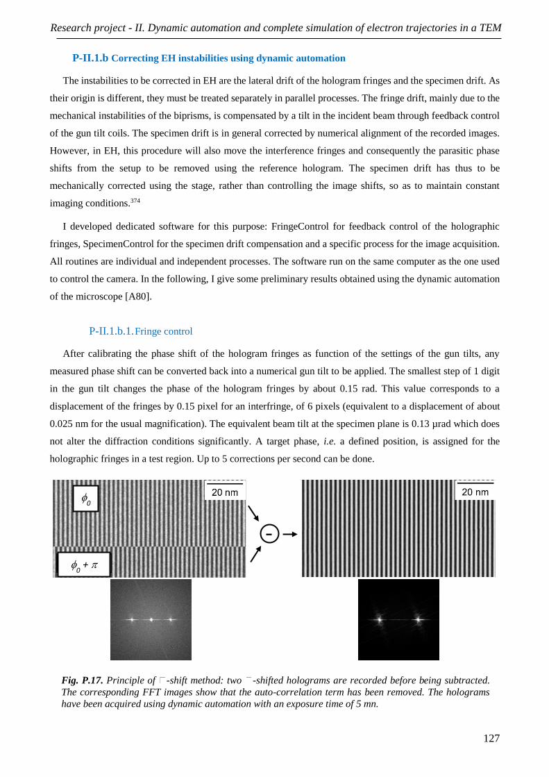
127
Research project - II. Dynamic automation and complete simulation of electron trajectories in a TEM
P-II.1.b Correcting EH instabilities using dynamic automation
The instabilities to be corrected in EH are the lateral drift of the hologram fringes and the specimen drift. As
their origin is different, they must be treated separately in parallel processes. The fringe drift, mainly due to the
mechanical instabilities of the biprisms, is compensated by a tilt in the incident beam through feedback control
of the gun tilt coils. The specimen drift is in general corrected by numerical alignment of the recorded images.
However, in EH, this procedure will also move the interference fringes and consequently the parasitic phase
shifts from the setup to be removed using the reference hologram. The specimen drift has thus to be
mechanically corrected using the stage, rather than controlling the image shifts, so as to maintain constant
imaging conditions.374
I developed dedicated software for this purpose: FringeControl for feedback control of the holographic
fringes, SpecimenControl for the specimen drift compensation and a specific process for the image acquisition.
All routines are individual and independent processes. The software run on the same computer as the one used
to control the camera. In the following, I give some preliminary results obtained using the dynamic automation
of the microscope [A80].
P-II.1.b.1. Fringe control
After calibrating the phase shift of the hologram fringes as function of the settings of the gun tilts, any
measured phase shift can be converted back into a numerical gun tilt to be applied. The smallest step of 1 digit
in the gun tilt changes the phase of the hologram fringes by about 0.15 rad. This value corresponds to a
displacement of the fringes by 0.15 pixel for an interfringe, of 6 pixels (equivalent to a displacement of about
0.025 nm for the usual magnification). The equivalent beam tilt at the specimen plane is 0.13 µrad which does
not alter the diffraction conditions significantly. A target phase, i.e. a defined position, is assigned for the
holographic fringes in a test region. Up to 5 corrections per second can be done.
-
0
0 +
Fig. P.17. Principle of -shift method: two -shifted holograms are recorded before being subtracted.
The corresponding FFT images show that the auto-correlation term has been removed. The holograms
have been acquired using dynamic automation with an exposure time of 5 mn.

128
Research project - II. Dynamic automation and complete simulation of electron trajectories in a TEM
An additional benefit of FringeControl allows advanced phase reconstruction methods to be implemented
such as the -shift method where a pair of holograms exactly phase shifted by are required for optimal use.335
By subtracting both holograms, the autocorrelation term is removed resulting to a large decrease of the noise
such as a part of the noise coming from the gain of the camera (Fig. P.17).
Fig. P.18.a shows how the phase (position) of the hologram fringes varied in the absence of fringe control
for two different measurements. Holograms with a fringe spacing of 1 nm (7 pixels) were recorded in empty
vacuum with and without control for up to 600 s. The first series (#1) at the beginning of the day had relatively
large drift (0.14 rad/s) and for the second (#2) after some hours, the drift was lower (0.04 rad/s). With feedback-
control, however, the phase of the hologram can be stabilized to a predefined target value, in this case 1 rad and
1- rad (Fig. P.18.b). The contrast of the fringes decreases on the uncorrected holograms as a function of total
acquisition time whilst the drift-compensated series maintained the initial contrast (Fig. P.18.c).
Fig. P.18.d shows the evolution of the phase noise over the time with and without FringeControl. The phase
extraction has been performed with a 2 nm of spatial resolution. Without feedback control, the phase noise
continuously increases due to the contrast decrease. When FringeControl is on, we can observe a lower value
d)
Fig. P.18. Fringe stabilization by real-time feedback control of the gun tilts: phase measurements of the
fringe position without (a) and with (b) feedback control as a function of the exposure time, and for two
acquisition series; (c) and (d) Contrast and phase noise of the corresponding recorded holograms. Note the
logarithmic scale for the phase noise.

129
Research project - II. Dynamic automation and complete simulation of electron trajectories in a TEM
of noise which remains stable over the time. This limit corresponds to the gain noise of the camera. Using an
automatic procedure for acquiring and subtracting -shifted holograms, the measured phase noise is much lower
and reaches few mrads. The more significant feature is the continuous noise reduction over time. These
preliminary experiments show that we are very close to reaching the theoretical limit of the counting noise in a
single hologram by using fringe-drift compensation.
P-II.1.b.2. Specimen control
The real-time compensation of the specimen drift is based on the same logic as for the fringe drift
compensation: diagnostics, calibration and control with an optimization of computing time. The diagnostic tool
is based on cross-correlations between a target and current image region after applying dedicated filters. A
region of the hologram with identifiable image features such as amorphous material or edges is suitable. Unlike
the fringe control, the displacement vector of the image with respect to a mechanical shift of the stage along two
axes must be calibrated. For small injections of mechanical shift, we found the action of the stage to be linear
and remarkably free from hysteresis. The smallest mechanical shifts move the specimen by 0.15 nm, far below
the spatial resolution in Lorentz mode (0.5 nm). This value is surprising as the displacement is only performed
by a pure mechanical system without piezo-electric displacements. Nevertheless, it remains too high to apply
this approach to atomic resolved electron holography.
Fig. P.19 demonstrates the efficiency of the dynamic automation for correcting the specimen drift on a Ni
nanowire. The uncorrected image obtained after 15 mn of exposure time without feedback control shows blurred
contours due to large drift (blue path) measured during the acquisition. On the contrary, the feedback control
allows the nanowire to be held in the same location with accuracy better than 0.5 nm (orange path).
The comparison of profiles extracted on the edge of the nanowire between uncorrected and corrected images
show that details as the presence of an oxide layer can be observed become visible on the corrected image.

130
Research project - II. Dynamic automation and complete simulation of electron trajectories in a TEM
P-II.1.b.3. Removal of both fringe and specimen instabilities
To illustrate the efficiency of removing both instabilities, Fig. P.20 displays a comparison between
holograms and corresponding phase image acquired with a usual exposure time of 5s and a smart controlled
sequence with p-shift method and long exposure time. Much lower phase noise can be obtained in the phase
image with automation, without specimen blurring, after 10 mn of total exposure time. The magnetic leakage
field can nicely be observed around the nanowire and looks like what can be obtained in simulation.
Fig. P.19. Specimen stabilization by real-time feedback control of the stage: resulting images of a Ni
nanowire after 15 mn of exposure time without (a) and with (b) feedback control; (c) Displacements of the
specimen measured in real time without (blue) and with (orange) correction; (d) Profiles extracted from the
lines on the resulting images showing blurred (blue) and well-defined (orange) edges.

131
Research project - II. Dynamic automation and complete simulation of electron trajectories in a TEM
P-II.1.c Future of dynamic automation
With dynamic automation, holograms can be routinely acquired over much longer times without otherwise
changing the experiment, or adding any heavy numerical processing as described in many papers. In theory, the
theoretical limit of SNR can be obtained using an unlimited acquisition time by actively compensating the
instrumental instabilities during acquisition. We reached a lowest value of phase noise equal to 2 mrad under
normal imaging conditions. However this value is limited by the reading noise of the camera on the I2TEM
(Gatan OneView) whose detector is composed of CMOS devices with a scintillator. The MTF and DQE could
be greatly improved if using of direct electron detection cameras. I have no doubt that the phase noise will be
much lower, allowing the measurement of very small phase shifts such as those involved in some of the
operando studies presented in section P-I. The investigation of spintronics devices, or semiconducting
nanowires for studying the Stark effect, will become accessible. I aim to define the best conditions (optical
alignment of the microscope, detector,…) for recording holograms with the best phase detection limit. A funding
has been requested for a direct electron detection camera which will be installed on the I2TEM microscope.
I want also to go deeper in the dynamic automation for improving the speed, sensitivity and accuracy of
instability analysis and correction. Others instabilities such as defocus could be corrected. Apart from the
necessity of a fast camera and microscope control protocols, the approach presented here is based on software
Fig. P.20. Comparison of holograms and corresponding phase images between an usual exposure time
of 5 s (top images) and dynamic automation during 10 mn with -shift method (bottom images). The
holograms have been recorded on a magnetic Ni nanowire. The phase noise has been strongly decreased
on the -shifted hologram recorded with 10 mn of exposure time.

132
Research project - II. Dynamic automation and complete simulation of electron trajectories in a TEM
routines and should therefore be widely applicable to others related TEM methods. I plan to transfer the dynamic
automation from the I2TEM microscope to others microscopes equipped with piezo-stage (stage with piezo-
actuators for atomic displacements) for performing high-resolution experiments while correcting the specimen
drift.
The dynamic automation also opens the way for performing new experiments in low dose conditions. Indeed,
long exposure times are not necessarily associated with high dose. For example, electron holograms acquired in
ultrafast TEM experiments suffer from extremely low beam intensities. Long exposure times of 150 s are even
mandatory to obtain exploitable phase images [A83]. I will thus transfer the dynamic automation on the new
HF3300 microscope actually developed for time-resolved studies in the framework of the joint-lab Hitachi-
CNRS HC-IUMi. Through different collaborations, I will also participate to studies in low dose conditions for
minimizing the charge effect of the specimen due to the electron beam or observing sensitive materials during
long exposure times.
P-II.2 Simulation and visualization of electron trajectories in a TEM
The emergence of new TEM instrumentation, pushing forward classical TEM techniques with higher spatial
and energy resolution, is also at the origin of new original techniques. These new methods of observations have
a high potential to study processes or physical quantities more precisely, or even to perform observations that
have not been possible until now. Related methods to electron spectroscopy or differential phase contrast (DPC)
in STEM are a huge growing field of innovations and original studies. For interferometric methods, an electron
biprism located before 3 magnetic condenser lenses offers for instance the possibility to create a tilted reference
wave (TRW) relatively to the object wave for direct measurement of the deformation field375, or to tune two
shifted half electron probe focused on the TEM sample plane to performed so-called Split Beam CBED
(SCBED) experiment.376 An alternative example is the introduction of adapted phase plate or the use of
aberration corrector multipolar optic377,378, in order to create vortex beams for new electron energy loss magnetic
chiral dichroism (EMCD) measurements (see section III.3) or more generally to perform phase manipulation.
In each case, particular lens conditions have been selected to adjust the desired configuration as well as the
amplitude of the phenomena. From a general point of view, TEM experiments require adjusting precise
configuration of the incident electron beam like controlled convergence angle and spot size, tilt of the reference
wave for off-axis electron holography… as well as fine-tuning of the imaging part of the column (i.e. particularly
in EH for which the overlap of the reference and the object beams has to be perfectly adjusted).
All these examples illustrate the advantages of such modern and versatile microscopes to settle peculiar and
complex optic configurations. However the fine adjustment of all the microscope parameters is not
straightforward and is barely optimized when fixed manually, even for well-established observations such as
high-resolution, electron spectroscopy or EH experiments. To optimize such experiments, microscopists would
then ideally need to simulate the optical configuration thanks to a complete model of the microscope which
could give, prior to any experiment, the optimal conditions (currents for the electromagnetic lenses and

133
Research project - II. Dynamic automation and complete simulation of electron trajectories in a TEM
deflectors, extraction, gun lens and acceleration voltage for the gun part) which should be used experimentally
to obtain the desired optical parameters (shift distance, tilt angles, magnification…).
In collaboration with F. Houdellier and M.J. Hÿtch (CEMES), I am developing a dedicated software for a
complete electron trajectory simulation of the I2TEM microscope. We aim at pushing forward the capabilities
of the I2TEM microscope by:
• being able to get the complete simulation of the microscope,
• monitoring all the currents in all optical part of it to set the initial optimal alignment for each given
experiment,
• automatically fine tuning the alignment to optimize the experimental data.
The design of each optical part of the I2TEM column is perfectly known and therefore accurate simulation
of the beam path through it can be carried out. In addition all the currents set in the I2TEM lenses, deflectors
and stigmators can be addressed by software (see section P-II.1) allowing setting the simulated configuration.
P-II.2.a SIMION software
Models based on trajectories computed through a succession of basic Glaser shape magnetic field and starting
from a fixed source optic have been developed in many research groups using different supports (Matlab,…).
However, these simulations do not take into account the saturation of magnetic lenses, which therefore limit
their use to small lens currents. Furthermore, these models are limited to a part of the microscope column and
do not consider the whole setup. They do not include any gun optic, as well as all the imaging optics, and are in
general limited to paraxial solutions. If these models are very useful from a conceptual point of view, strong
differences emerge when increasing tilt or shift amplitude, especially when lenses saturations and aberrations
become non-negligible.
Being able to precisely calculate the correct optical setting under real conditions requires the development
of a more complete model from the emission of electrons to their detection on the detector plane. This simulation
has to be able to retrieve the electrons trajectories in a full model, which will combine a wide range of scale,
starting from nanometer size of the electron source to the whole column length (meter). The optical component
real design exported for Computer-Aided Design (CAD) model (electrodes shape, material…) has to be used to
calculate all the potentials (electric and magnetics) encountered by the electron beam. In addition, a three-
dimensional model required in order to properly simulate even the non-cylindrical symmetry element as
electrostatic biprisms.
Many commercial electron optics simulations software encountered in the literature are used to address
various needs, depending on the user interest.379–381 Few software can be used to precisely design one isolated
component, (like an electromagnetic lens, an electron mirror system, …) or a small optical system (like a lens
doublet, …) providing a multitude of very useful and precise quantitative information as off axial aberrations
coefficients, magnetic field shape, … However a large part of these software are strongly limited when dealing
with a large numbers of optical elements.380,381 The SIMION software379 solves the Laplace equation using Finite
Difference Method in order to retrieve the potential distribution inside a three-dimensional or a cylindrical

134
Research project - II. Dynamic automation and complete simulation of electron trajectories in a TEM
symmetric electron/ion optical component within a certain numbers of known conditions on the boundary
surface enclosing the component volume. This volume is called a “Potential Array” in SIMION language from
which electrons (or ions trajectories) are retrieved thanks to standard Newton equations of motion. CAD model
of any electron optic component can be easily imported and converted in a potential array. Regarding the full
TEM simulation, SIMION offers the possibility to add many potential arrays, i.e. many optical component, in
a global “ion optic workbench” easy to manipulate/modify and compute. Furthermore, potential array with
strong size difference (like the nanometer size field emission tip and the 60 cm long standard linear accelerator)
can be easily associated and the potential distribution can then be computed using different meshing size
depending on the precision requested. The main drawback of SIMION concerns the magnetic optical
components: only magnetic scalar potential, with poles of infinite permeability, can be modelled with so-called
magnetic Potential Arrays.
P-II.2.b First results of a complete simulation of electron trajectories in a TEM
This project started in 2016 during the internship of a Hitachi engineer (Y. Kubo) who worked on the first
version of the software [A73] including SIMION capabilities. A PhD student (J. Dupuy) is actually in charge
of the new version of the software. The first version of the software includes the gun, all lenses (x9) and biprisms
(x4) of the I2TEM microscope. All lenses and the gun potential were calculated in two-dimensional (2D) using
cylindrical symmetric coordinates. The electrostatic biprism and deflectors which do not present any cylindrical
symmetry were considered in a three dimensional (3D) coordinate system. The final workbench which finally
combines all the elements was defined in the three dimensional coordinates system. For cylindrical symmetric
component, the 2D representation of the calculated field is sufficient. However, the Larmor rotation taking place
in a magnetic lens implies to display the electrons trajectories in 3D. I will not describe in the following the
calculation of each individual element. All details, as the calculation of the real size high voltage cold field
emission source, the weak magnetic lenses (saturated and non-saturated), the objective lens (strong magnetic
lens) and electrostatic Möllenstedt biprism, can be found in reference [A73].
The combination of all separated optical elements in our software allowed designing a complete model of
the I2TEM microscope from the top (field emission tip surface) down to the detector plane. In order to achieve
this complete simulation, we used the concept of “Ion Optic Workbench” (IOB) defined in SIMION.379 The
IOB is an imaginary volume in space in which all potential arrays calculated previously can be sized and
combined. It is however of large importance to notice that electrostatic and magnetic fields can only exist within
the potential array, and regions between arrays are assumed to be field free. As a consequence, all boundary
conditions between each potential array need to be properly adjusted.
Using the first version of the software, we successfully plotted the electrons trajectories from the electron
source to the detector plane. Fig. P.21 shows the simulations obtained for the I2TEM column set in TEM mode
with a magnification of x10000. Source conditions and lens excitations are displayed on the right part of Fig.
P.21. The spherical aberration corrector inserted between the objective lens and the first intermediate lens (I1)
is not taken into account into the simulations, as the associated magnification is equal to 1 . However, the

135
Research project - II. Dynamic automation and complete simulation of electron trajectories in a TEM
corrector has to be considered if we want to deal with aberrations effects (higher order effects on the trajectories).
Most applications do not require this refinement but the corrector may be added in a future version of the
simulation.
A large number of optical configurations used for various applications can now be simulated using this first
version from off-axis electron holography with the proper handling of hologram fields of view to electron
diffraction (parallel and convergent) with the determination of arbitrary camera length, convergence angles and
even TEM and STEM imaging.
Fig. P.21. Full electrons trajectories simulations for I2TEM microscope. The (x, z) and (y, z) planes are
reported and enlarged in the direction x and y by a factor of 800. The red dashed line rectangles after the
P2 lens show the electron trajectories in (x, z) and (y, z) enlarged in x and y direction by a factor of 40.
Indeed, the angles are much larger in this region to project on the scintillator of the camera. In the small
red filled line rectangles are also reported the detailed trajectories around the sample plane.

136
Research project - II. Dynamic automation and complete simulation of electron trajectories in a TEM
In reference [A73], we illustrated the capabilities of this approach to simulate two specific non-trivial
configurations to highlight the strength of the model for both the illumination part of the microscope and the
imaging part. For instance, the magnification of the first image, produced by the objective lens of a TEM, is
managed by a combination of intermediate and projectors lenses excitations (5 different lenses in the case of
I2TEM). The magnification table, generated by all manufacturers during factory alignment, is not continuous
and consists of specific lenses current values determined to magnify the image at particular magnifications
without introducing any Larmor rotation between them. It is thus not possible to choose any arbitrary value of
magnification when required. Using the first version of the software, an arbitrary magnification without Larmor
rotation was easily set calculating all the currents values Fig. P.22). This apparently simple application remains
almost impossible to implement manually.
Fig. P.22. Simulation of the electrons trajectories calculated for an arbitrary magnification of 25kX at 300
kV. Only the imaging part of the I2TEM column, in (x,z) and (y, z) planes, is displayed. The images of a
cross-grating calibration sample obtained for 20kX, 25kX and 30kX are also reported. The pixel size of the
used one-view camera is15 μm.

137
Research project - II. Dynamic automation and complete simulation of electron trajectories in a TEM
However our approach presents some weak points. Indeed, making a complete simulation requires an open
access to all technical drawings of each optical element of the microscope, which can be difficult to obtain from
manufacturers. The model also requires a calibration step, which can be time-consuming. Computation time of
a standard simulation of the complete electron trajectory is between 2 and 5 min depending on the desired
accuracy. The visualization of the electron trajectories is also not trivial and needs to be improved. All these
minor weak points restrict at the moment the use of such type of simulation to specialized centres. It is however
highly desirable that in near future, TEM manufacturers could offer such complete simulation to users.
P-II.2.c Future developments
I strongly believe that such simulations
consistently associated with modern and optically
complex machines will significantly open the field
of possibilities in transmission electron
microscopy. This approach can be extended to any
other situations encountered by (S)TEM users.
Such system, which will provide standard
characterizations methods (from electron
diffraction, to EH through conventional high
resolution, STEM or EFTEM...) could also be used
as an "electron optical bench "in the same way as
laser optical benches used in various fields of
modern physics, will determine innovative optical
configurations necessary for the optimal use of the
TEM. For example, these simulations could be
very useful in operando EH experiments detailed
in section P-I to define and optimize the hologram
field of view and the interference fringes
periodicity. The configuration using two biprisms
in the imaging system185 is used to independently
adjust these two parameters, but it does not allow
the easy access to any combination of fields of
views / interference fringes distances possible that
may be of interest for various experimental cases.
The simulation makes possible to adjust all the
optical parameters to determine the electron
trajectories and therefore obtain the microscope
parameters necessary for an optimal experiment.
Fig. P.23. Human-machine interface recently developed.

138
Research project - II. Dynamic automation and complete simulation of electron trajectories in a TEM
All the simulated parameters are then used to set all the microscope lenses and the users will have a rapid access
to the optimal configuration of the TEM required for the experiment.
I plan to continue the development of the simulation software and to solve the few weak points. A PhD
student (J. Dupuy) has been hired to introduce deflectors into the simulation, to optimize the speed of processing
and to develop homemade software based on the paraxial approximation as well as a direct communication
between the software and the microscope. In parallel, we are developing a dedicated human-machine interface
for an intuitive and user-friendly visualization of electron trajectories (Fig. P.23), and to set the input values
required for computing these electron trajectories using SIMION or using the software based on the paraxial
approximation for decreasing the computing time. This interface will also allow a direct communication
between the microscope and the simulation software. The work on this interface started with students of the
“Human-Machine Interface” master (ENAC-University Paul Sabatier of Toulouse) in 2019 and now continues
with a 6 month postdoc.
In addition to developing and optimizing TEM configurations, I aim to generalize this approach to all non-
trivial TEM experiments in a fully automated procedure. The user would set a specific target either for the
illumination optics (like tilts angles, shifts...) or/and for the image and diffraction modes (as magnification,
camera length, field of view...). The optical parameters will then be adjusted in the simulated model to reach
the target requirement for an optimal set of TEM parameters. These calculated parameters will be introduced
thanks to the human-machine interface into the microscope server to set the optimal starting alignment. To
optimize even more the experiment, an in-line analysis of the experimental data could then performed with a
feedback loop to the TEM parameters. The automated in-line procedure to optimize the TEM configuration will
be combined to the loop adjustment algorithm based on real time data treatment and analysis (see section P-
II.1) and will strongly benefit to the operando EH experiments (section P-I).
Conclusion
My research project for the coming years aims at pushing forward the studies of physical quantities
and processes by TEM. I want to improve the sensitivity and spatial resolution in EH to measure weaker
and more localized phenomena. The operando studies will make it possible to define a methodology in
order to electrically contact any sample or device and quantitatively map its properties under current or
voltage. These investigations thus pave the way for an in-depth and original study of electromagnetic
properties at the nanometer scale.
This project also includes original developments in transmission electron microscopy (dynamic
automation, simulation of full electron trajectories). If these developments will first be applied to EH,
they will also impact other techniques and benefit all in situ/operando studies.

139
Publications in peer-reviewed scientific journals
PUBLICATIONS IN PEER-REVIEWED SCIENTIFIC JOURNALS
Articles
A87 Exotic transverse-vortex magnetic configurations in CoNi nanowires
I.M. Andersen, L.-A. Rodriguez, C. Bran, C. Marcelot, S. Joulié, T. Hungria, M. Vazquez, C. Gatel and
E. Snoeck
ACS Nano 14, 1399 (2020)
A86 One-pot seed-mediated growth of Co nanoparticles by the polyol process: unreavaling the
heterogeneous nucleation step
R.K. Ramamoorthy, A. Viloa, B. Grindi, J. Peron, C. Gatel, M.J. Hÿtch, R. Arenal, L. Sicard, M. Giraud,
J.-Y. Piquemal and G. Viau
Nano Letters 19, 9160 (2019)
A85 Multi magnetic states in Co/Cu multilayered nanocylinders studied by combination of off-axis electron
holography imaging and micromagnetic simulations
N. Biziere, D. Reyes, T. Wade, B. Warot-Fonrose and C. Gatel
J. Appl. Phys. 126, 163906 (2019)
A84 Holographic Vector Field Electron Tomography of Three-Dimensional Nanomagnets
D. Wolf, N. Biziere, S. Sturm, D. Reyes, T. Wade, T. Niermann, J. Krehl, B. Warot-Fonrose, B.
Büchner, E. Snoeck, C. Gatel and A. Lubk
Communication Physics 2, 1-9 (2019)
A83 Optimization of off-axis electron holography performed with femtosecond electron pulses
F. Houdellier, G.-M Caruso, S. Weber, M.J. Hÿtch, C. Gatel and A. Arbouet
Ultramicroscopy 202, 26-32 (2019)
A82 Magnetic imaging using geometrically constrained nano-domain walls
H. Corte-Leon, L.-A. Rodriguez, M. Pancaldi, C. Gatel, D. Cox, E.Snoeck, V. Antonov, P. Vavassori
and O. Kazakova
Nanoscale 11, 4478-4488 (2019)
A81 Nanoparticle ripening: A versatile approach for the size and shape control of metallic iron
nanoparticles
L.-M. Lacroix, A. Meffre, C. Gatel, P.-F. Fazzini, S. Lachaize, M. Respaud and B. Chaudret
ChemPlusChem 84, 302-306 (2019)
A80 Unlimited acquisition time in electron holography by automated feedback control of transmission
electron microscope
C. Gatel, J. Dupuy, F. Houdellier and M.J. Hÿtch
Appl. Phys. Letters 113, 133102 (2018)
A79 Magnetic-field induced rotation of magnetosome chains in silicified magnetotactic bacteria
M. Blondeau, Y. Guyodo, F. Guyot, C. Gatel, N. Menguy, I. Chebbi, B. Haye, M. Durand-Dubief, E.
Alphandery, R. Brayner and T. Coradin
Scientific Reports 8, 7699 (2018)
A78 Air-stable Anisotropic Monocrystalline Nickel Nanowires Characterized using Electron Holography
G.L. Drisko, C. Gatel, P.-F. Fazzini, A. Ibarra, S. Mourdikoudis, V. Bley, K. Fajerwerg, P. Fau and
M.L. Kahn
Nano Letters 18, 1733-1738 (2018)

140
Publications in peer-reviewed scientific journals
A77 Platinum tripods as nanometric frequency multiplexing devices
B. Camargo, B. Lassagne, R. Arenal, C. Gatel, T. Blon, G. Viau, L.-M. Lacroix and W. Escoffier
Nanoscale 9, 14635-14640 (2017)
A76 Inhomogeneous spatial distribution of the magnetic transition in an iron-rhodium thin film
C. Gatel, B. Warot-Fonrose, N. Biziere, L.A. Rodriguez, D. Reyes, R. Cours, M. Castiella and M.-J.
Casanove
Nature Communications 8, 15703 (2017)
A75 Role of internal demagnetizing field for the dynamics of a surface-modulated magnonic crystal
M. Langer, F. Röder, R.A. Gallardo, T. Schneider, S. Stienen, C. Gatel, R. Hubner, L. Bischoff, K.
Lenz, J. Lindner, P. Landeros and J. Fassbender
Phys. Rev. B 95, 184405 (2017)
A74 In Depth Spatially Inhomogeneous Phase Transition in Epitaxial MnAs Film on GaAs(001)
C. Gatel, X. Fu, V. Serin, M. Eddrief, V. Etgens and B. Warot-Fonrose
Nano Letters, 17, 2460-2466 (2017)
A73 Optimising electron microscopy experiment through electron optics simulation
Y. Kubo, C. Gatel, E. Snoeck and F. Houdellier
Ultramicroscopy, 175, 67-80 (2017)
A72 Assessment of off-axis and in-line electron holography for measurement of potential variation in
Cu(In,Ga)Se2 thin-film solar cells
D. Keller, S. Buecheler, P. reinhard, F. Pianezzi, E. Snoeck, C. Gatel, M.D. Rossell, R. Erni and A.N.
Tiwari
Advanced Structural and Chemical Imaging 2, 1 (2017)
A71 Magnetism and morphology in faceted B2-ordered FeRh nanoparticles
M. Liu, P. Benzo, H. Tang, M. Castiella, B. Warot-Fonrose, N. Tarrat, C. Gatel, M. Respaud, J.
Morillo and M.-J. Casanove
EPL, 116, 2706 (2016)
A70 Quantitative Nanoscale Magnetic Study of Isolated Diameter-Modulated FeCoCu Nanowires
L.A. Rodriguez, C. bran, D. Reyes, E. Berganza, M. Vasquez, C. Gatel, E. Snoeck and A. Asenjo
ACS Nano 10, 9669-9678 (2016)
A69 Dynamical holographic Moires in a TEM
C. Gatel, F. Houdellier and E. Snoeck
J. Phys..D: Applied Physics 49, 324001 (2016)
A68 Highly strained AlAs-type interfaces in InAs/AlSb heterostructures
M. Vallet, Y. Claveau, B. Warot-Fonrose, C. Gatel, J. Nicolai, N. Combe, C. Magen, R. Teissier,
A.N. Baranov and A. Ponchet
Appl. Phys. Letters 108, 211908 (2016)
A67 Quantitative 3D electromagnetic field determination of 1D nanostructures from single projection
C. Phatak, L. de Knoop, F. Houdellier, C. Gatel, M.J. Hytch and A. Masseboeuf
Ultramicroscopy 164, 24-30 (2016)
A66 Magnetic Configurations in Co/Cu Multilayered Nanowires: Evidence of Structural and Magnetic
Interplay
D. Reyes, N. Biziere, B. Warot-Fonrose, T. Wade and C. Gatel
Nano Letters 16, 1230-1236 (2016)

141
Publications in peer-reviewed scientific journals
A65 Enhanced magnetization at the Cr/MgO(001) interface
M.-A. Leroy, A.M. Bataille, Q. Wang, M.R. Fitzsimmons, F. Bertran, P. Le Fevre, A. Taleb-Ibrahimi,
A. Vlad, A. Coati, Y. Garreau, T. Hauet, C. Gatel, F. Ott and S.Andrieu
Appl. Phys. Letters 107, 251602 (2015)
A64 Structural investigation of magnetic FeRh epitaxial films
M. Castiella, C. Gatel,J.F. Bobo, N. Ratel-Ramond, R.P. Tan, M. Respaud and M.-J.Casanove
Mater. Res. Express 2, 086401 (2015)
A63 Size-Specific Spin Configurations in Single Iron Nanomagnet: From Flower to Exotic Vortices
C. Gatel, F.J. Bonilla, A. Meffre, E. Snoeck, B. Warot-Fonrose, B. Chaudret, L.-M. Lacroix and T.
Blon
Nano Letters 15, 6952-6957 (2015)
A62 3D Magnetic Induction Maps of Nanoscale Materials Revealed by Electron Holographic Tomography
D. Wolf, L.A. Rodriguez, A. Beche, E. Javon, L. Serrano, C. Magen, C. Gatel, A. Lubk, H. Lichte, S.
Bals, G. Van Tendeloo, A. Fernandez-Pacheco, J.-M. De Teresa and E. Snoeck
Chemistry of Materials 27, 6771-6778 (2015)
A61 Formation of strained interfaces in AlSb/InAs multilayers grown by molecular beam epitaxy for
quantum cascade lasers
J. Nicolai, B. Warot-Fonrose, C. Gatel, R. Teissier, A.N. Baranov, C. Magen and A. Ponchet
J. Appl. Phys 118, 035305 (2015)
A60 Low-noise cold-field emission current obtained between two opposed carbon cone nanotips during in
situ transmission electron microscope biasing
L. de Knoop, C. Gatel, F. Houdellier, M. Monthioux, A. Masseboeuf, E. Snoeck and M.J. Hÿtch
Appl. Phys. Lett. 106, 263101 (2015)
A59 In situ electron holography of the dynamic magnetic field emanating from a hard-disk drive writer
J.F. Einsle, C. Gatel, A. Masseboeuf, R. Cours, M.A. Bashir, M. Gunbbins, R.M. Bowman and E.
Snoeck
Nano Research 8, 1241-1249 (2015)
A58 Development of TEM and SEM high brightness electron guns using cold-field emission from a carbon
nanotip
F. Houdellier, L. de Knoop, C. Gatel, A. Masseboeuf, S. Mamishin, Y. Taniguchi, M. Delmas, M.
Monthioux, M.J. Hÿtch and E. Snoeck
Ultramicroscopy 151, 107-115 (2015)
A57 Air- and Water-Resistant Noble Metal Coated Ferromagnetic Cobalt Nanorods
S. Lentijo-Mozo, R.P. Tan, C. Garcia-Marcelot, T. Altantzis, P.F. Fazzini, T. hungria, B. Cormary,
J.R. Gallagher, J.T. Miller, H. Martinez, S. Schrittwieser, J. Schotter, M. Respaud, S. Bals, G. Van
Tendeloo, C. Gatel and K. Soulantica
ACS Nano 9, 2792-2804 (2015)
A56 Sb surfactant mediated growth of InAs/AlAs0.56Sb0.44 strained quantum well for intersubband absorption
at 1.55 µm
Y. Zhao, J. Nicolai, N. Bertru, H. Folliot, M. Perrin, C. Gatel, B. Warot-Fonrose and A. Ponchet
App. Phys. Lett. 106, 081908 (2015)
A55 Crystal growth of bullet-shaped magnetite in magnetotactic bacteria of the Nitrospirae phylum
J.H. Li, N. Menguy, C. Gatel, V. Boureau, E. Snoeck, G. Patriarche, E. Leroy and Y.X. Pan
Journal of the Royal Society, Interface / the Royal Society 12, 20141288 (2015)

142
Publications in peer-reviewed scientific journals
A54 Dynamical effects in strain measurements by dark-field electron holography
E. Javon, A. Lubk, R. Cours, S. Reboh, N. Cherkashin, F. Houdellier, C. Gatel and M. Hÿtch
Ultramicrocopy 147, 70-85 (2014)
A53 High resolution imaging of remanent state and magnetization reversal of superdomain structures in
high-density cobalt antidot arrays
L.-A. Rodríguez, C. Magen, E. Snoeck, C. Gatel, C. Castán-Guerrero, J. Sesé, L.M. García, J. Herrero-
Albillos, J. Bartolomé, F. Bartolomé and M.R. Ibarra
Nanotechnoloy 25, 385703 (2014)
A52 Epitaxial growth micro-structure and magnetic studies of FePt nanoparticles: MgO multi-layer
composite thin films
J.-B. Wu, M.-J. Zhou, X.-M. Wang, Y.Y. Waang, Z.W. Xiong, X.L. Cheng, M.-J. Casanove, C. Gatel
and W.D. Wu
Acta Physica Sinica 63, 166801 (2014)
A51 Determining the work function of a carbon-cone cold-field emitter by in situ electron holography
L. de Knoop, F. Houdellier, C. Gatel, A. MasseBoeuf, M. Monthioux and M.J. Hÿtch
Micron 63, 2-8 (2014)
A50 Tunnel-mediated coupling between antiferromagnetic thin films
M.-A. Leroy, A.M. Bataille, B. Dkhil, F. Porcher, A. Barbier, V.L.R. Jacques, C. Bellouard, T. Hauet,
S. Ravy, J. Herrero-Martin, C. Gatel, K. Bouzehouane, A. Gukasov, S. Andrieu and C. Tiusan
Phys. Rev. B 90, 035432 (2014)
A49 Co–Fe Nanodumbbells: Synthesis, Structure, and Magnetic Properties
N. Liakakos, C. Gatel, T. Blon, T. Altantzis, S. Lentijo-Mozo, C. Garcia-Marcelot, L.-M. Lacroix, M.
Respaud, S. Bals, G. Van Tendeloo and K. Soulantica
Nano Letters 14, 2747-2754 (2014)
A48 Structure, magnetic ordering and spin filtering efficiency of NiFe2O4(111) ultrathin films
S. Matzen, J.-B. Moussy, P. Wei, C. Gatel, J.C. Cezar, M.A. Arrio, Ph. Sainctavit and J.S. Moodera
Appl. Phys. Lett. 104, 182404 (2014)
A47 Experimental investigation of the vibrational density of states and electronic excitations in metallic
nanocrystals
M. Bayle, P. Benzo, N. Combe, C. Gatel, C. Bonafos, G. Benassayag, and R. Carles
Phys. Rev.B,89, 195402 (2014)
A46 Molecular beam epitaxy and properties of GaAsBi/GaAs quantum wells grown by molecular beam
epitaxy – Effect of thermal annealing
H. Makhloufi, P. Boonpeng, S. Mazzucato, J. Nicolai, A. Arnoult, T. Hungria, G. Lacoste, C. Gatel, A.
Ponchet, H. Carrere, X. Marie and C. Fontaine
Nanoscale Research Letters 9:123 (2014)
A45 Elastic strains at interfaces in InAs/AlSb multilayer structures for quantum cascade lasers
J. Nicolai, C. Gatel, B. Warot-Fonrose, R. Teissier, A.N. Baranov, C. Magen and A.Ponchet
Appl. Phys. Lett. 104, 031907 (2014)
A44 Dynamic scattering theory for dark-filed electron holography of 3D strain fields
A. Lubk, E. Javon, N. Cherkashin, S. Reboh, C. Gatel and M. Hÿtch
Ultramicrocopy 136, 42-49 (2014)
A43 Quantitative in situ magnetization reversal studies in Lorentz microscopy and electron holography
L.A. Rodriguez, C. Magen, E. Snoeck, C. Gatel, L. Marin, L. Serrano-Ramon, J.L. Prieto, M. Muñoz,
P.A. Algarabel, L. Morellon, J.M. De Teresa and M.R. Ibarra
Ultramicrocopy 134, 144-154 (2013)

143
Publications in peer-reviewed scientific journals
A42 Magnetism of CoFe2O4 ultrathin films on MgAl2O4 driven by epitaxial strains
C. Gatel, B. Warot-Fonrose, S. Matzen and J.-B. Moussy
Appl. Phys. Lett. 103, 092405 (2013)
A41 TEM study of structural hardening in a new martensitic steel for aeronautic application
F. Pettinari-Sturmel, B. Kedjar, J. Douin, C. Gatel, D. Delagnes and A. Coujou
Materials Science & Engineering A 576, 290-297 (2013)
A40 Counting elementary charges on nanoparticles by electron holography
C. Gatel, A. Lubk, G. Pozzi, E. Snoeck and M. Hÿtch
Phys. Rev. Lett. 111, 025501 (2013)
A39 Contrast enhancement of data measured with area detectors: a way to generalize the use of neutron
diffraction for thin film studies
A.M. Bataille, V. Auvray, C. Gatel and A. Gukasov
J. of Applied Crystallography 46, 726-735 (2013)
A38 Imaging the fine structure of a magnetic domain wall in a Ni nanocylinder
N. Bizière, C. Gatel, R. Lassalle-Balier, M.-C. Clochard, J.-E. Wegrowe and E. Snoeck
Nano Letters 13, 2053-2057 (2013)
A37 Optimized cobalt nanowires for domain wall manipulation imaged by in-situ Lorentz microscopy
L.A. Rodriguez, C. Magen, E. Snoeck, L. Serrano-Ramon, C. Gatel, R. Cordoba, E. Martinez-Vecino,
L. Torres, J.M. De Teresa and M.R. Ibarra
Appl. Phys. Lett. 102, 022418(2013)
A36 Investigation of high quality magnetite thin films grown on SrTiO3(001) substrates by pulsed laser
deposition
A. Hamie, Y. Dumont, E. Popova, A. Fouchet, B. Warot-Fonrose, C. Gatel, E. Chikoidze, J. Scola, B.
Berini and N. Keller
Thin Solid Films 525, 115-120 (2012)
A35 Stabilizing Vortices in Interacting Nano-Objects: A Chemical Approach
L.-M. Lacroix, S. Lachaize, F. Hue, C. Gatel, T. Blon, R. P. Tan, J. Carrey, B. Warot-Fonrose, and B.
Chaudret
Nano Letters 12, 3245-3250 (2012)
A34 Tuning complex shapes in platinum nanoparticles: from cubic dendrites to fivefold stars
L.-M. Lacroix , C. Gatel, R. Arenal, C. Garcia, S. Lachaize, T. Blon, B. Warot-Fonrose, E. Snoeck, B.
Chaudret and G. Viau
Angewandte Chemie 51(9), 4690-4694 (2012)
A33 A new linear transfer theory and characterization method for image detectors. Part II: Experiment
A. Lubk, F. Roeder, T. Niermann, C. Gatel, S. Joulié, F. Houdellier, C. Magen and M.J. Hÿtch
Ultramicroscopy 115, 78-87 (2012)
A32 Measurement and modeling of the elastic strain around nanoprecipitates
M. Le Fournier , J. Douin, C. Gatel, F. Pettinari-Sturmel et P. Donnadieu
Revue de métallurgie 109, 409-414 (2012)
A31 Mechanisms of epitaxy and defects at the interface in ultrathin YSZ films on Si(001)
P. de Coux, R. Bachelet, C. Gatel, B. Warot-Fonrose, J. Fontcuberta and F. Sanchez
CRYSTENGCOMM 14, 7851-7855 (2012)

144
Publications in peer-reviewed scientific journals
A30 Ultrasmall Functional Ferromagnetic Nanostructures Grown by Focused Electron-Beam-Induced
Deposition
L. Serrano-Ramon, R. Cordoba, L.A. Rodriguez, C. Magen, E. Snoeck, C. Gatel, I. Serrano, M.R. Ibarra
and J.M. De Teresa
ACS Nano 5, 7781-7787 (2011)
A29 Restoration of bulk magnetic properties by strain engineering in epitaxial CoFe2O4 (001) ultrathin films
S. Matzen, J.-B. Moussy, R. Mattana, F. Petroff, C. Gatel, B. Warot-Fonrose, J. C. Cezar, A. Barbier,
M.-A. Arrio and Ph. Sainctavit
Appl. Phys. Lett. 99, 052514 (2011)
A28 Epitaxial growth and ferrimagnetic behavior of MnFe 2O4(111) ultrathin layers for room-temperature
spin filtering
S. Matzen, J.-B. Moussy, R. Mattana, K. Bouzehouane, C. Deranlot, F. Petroff, J. C. Cezar, N.
Brookes, M.-A. Arrio, Ph. Sainctavit, C. Gatel and B. Warot-Fonrose
Phys. Rev. B 83, 184402 (2011)
A27 Microstructure and interface studies of LaVO3/SrVO3 superlattices
P. Boullay, A. David, W. C. Sheets, U. Lüders, W. Prellier, H. Tan, J. Verbeeck, G. Van Tendeloo, C.
Gatel, G. Vincze and Z. Radi
Phys. Rev. B 83, 125403 (2011)
A26 Structure and chemical order in FeRh nanoalloys epitaxially grown on MgO(001)
J. Ayoub, C. Gatel, C. Roucau and M.-J. Casanove
J. of Crystal Growth 314, 336-340 (2011)
A25 Use of long chain amine as a reducing agent for the synthesis of high quality monodisperse iron(0)
nanoparticles
A. Meffre, S. Lachaize, C. Gatel, M. Respaud and B. Chaudret
J. of Materials Chemistry 21, 13464-13469(2011)
A24 Magnetic field strength and orientation effects on Co-Fe discontinuous multilayers close to percolation
H.G. Silva, A.M. Pereira, J.M.Teixeira, J.M. Moreira, G.N. Kakazei, J.P. Araujo, Y.G. Pogorelov, J.B.
Sousa, M.E. Braga, B. Raquet, H. Rakoto, C. Gatel, E. Snoeck, S. Cardoso and P.P. Freitas
Phys. Rev.B 82, 144432 (2010)
A23 Achievement of InSb Quantum Dots on InP(100) Substrates
W. Lu, T. Rohel, N. Bertru, H. Folliot, C. Paranthoën, J.- M. Jancu, A. Létoublon,
A. Le Corre, C. Gatel, A. Ponchet, N. Combe, J.- M. Ulloa and P. Koenraad
Jp. J. Appl. Phys. 49, 060210 (2010)
A22 Analysis by high-resolution electron microscopy of elastic strain in thick InAs layers embedded in
Ga0.47In0.53As buffers on InP(001) substrate
C. Gatel, H. Tang, C. Crestou, A. Ponchet, N. Bertru, F. Doré, H. Folliot
Acta Materiala 58, 3238-3246 (2010)
A21 Microstructure and mechanical properties of ultrafine-grained fcc/hcp cobalt processed by a bottom-
up approach
F. Fellah, G. Dirras, J. Gubicza, F. Schoenstein, N. Jouini, S.M. Cherif, C. Gatel, J. Douin
Journal of Alloys and Compounds 489, 424-428 (2010)
A20 Lorentz microscopy mapping for domain walls structure study in L10 FePd thin films
A. Masseboeuf, C. Gatel, P. Bayle-Guillemaud, A. Marty and J.-C. Toussaint
Ultramicroscopy 110, 20-25 (2009)

145
Publications in peer-reviewed scientific journals
A19 Distortion corrections of ESI data cubes for magnetic studies
C. Gatel, B. Warot-Fonrose and P. Schattschneider
Ultramicroscopy 109, 1465-1471 (2009)
A18 The use of Lorentz microscopy for the determination of magnetic reversal mechanism of exchange-
biased Co30Fe70/NiMn bilayer
A. Masseboeuf, C. Gatel, P. Bayle-Guillemaud, Y. Lamy and B. Viala
J. Magn. Magn. Mater. 321, 3080-3083 (2009)
A17 Quantitative observation of magnetic flux distribution in new magnetic films for future high density
recording media
A. Masseboeuf, A. Marty, P. Bayle-Guillemaud, C. Gatel and E. Snoeck
Nano Letters 9, 2803–2806 (2009)
A16 Exchange bias in Co1-xNix/CoO core-shell nanowires: role of the antiferromagnetic superparamagnetic
fluctuations
T. Maurer, F. Zighem, F. Ott, G. Chaboussant, G. André, Y. Soumare, J.-Y. Piquemal, G. Viau and C.
Gatel
Phys. Rev.B, 80, 064427 (2009)
A15 Magnetic Configurations of 30 nm Iron Nanocubes Studied by Electron Holography
E. Snoeck, C. Gatel, L.-M. Lacroix, T. Blon, S. Lachaize, J. Carrey, M. Respaud and B. Chaudret
Nano Letters 8, 4293-4298 (2008)
A14 Optimal aperture sizes and positions for EMCD experiments
J. Verbeeck, C. Hébert, P. Schattschneider, S. Rubino, P. Novak, J. Rusz, F. Houdellier and C. Gatel
Ultramicroscopy 108, 865-872 (2008)
A13 Room temperature spin filtering in epitaxial cobalt-ferrite tunnel barriers
A.V. Ramos, M.-J. Guittet,J.-B. Moussy, R. Mattana, C. Deranlot, F. Petroff and C. Gatel
Appl. Phys. Lett. 91, 122107 (2007)
A12 Experimental application of sum rules for electron energy loss magnetic chiral dichroism
L. Calmels, F. Houdellier, B. Warot-Fonrose, C. Gatel, M.J. Hytch, , V. Serin, E. Snoeck and P.
Schattschneider
Phys. Rev.B. 76, 060409 (2007)
A11 Influence of a metallic or oxide top layer in epitaxial magnetic bilayers containing CoFe2O4(111) tunnel
barriers
A.V. Ramos, J.-B. Moussy, M.-J. Guittet, M. Gautier-Soyer, C. Gatel and P. Bayle-Guillemaud
Phys. Rev.B. 75, 224421 (2007)
A10 Epitaxial growth of Au and Pt on Fe3O4(111) surface
C. Gatel and E. Snoeck
Surface Science 601, 1031-1039 (2007)
A9 Magnetotransport properties of Fe3O4 epitaxial thin films: Thickness effects driven by antiphase
boundaries
A.V. Ramos, J.-B. Moussy, M.-J. Guittet, A.M. Bataille, M. Gautier-Soyer, M. Viret, C. Gatel , P.
Bayle-Guillemaud and E. Snoeck
J. App. Phys. 100, 103902 (2006 )
A8 Characterization of antiphase boundary network in Fe3O4(111) epitaxial thin films: Effect on
anomalous magnetic behavior
A. M. Bataille, L. Ponson, S. Gota, L. Barbier, D. Bonamy, M. Gautier-Soyer, C. Gatel and E. Snoeck
Phys. Rev.B. 74, 155438 (2006)

146
Publications in peer-reviewed scientific journals
A7 Comparative study of Ag, Au and Pt growth on Fe3O4(001)
C. Gatel and E. Snoeck
Surface Science 600, 2650-2662 (2006)
A6 Experimental evidence of the spin-dependence of electrons reflection in magnetic CoFe2O4/Au/Fe3O4
trilayers
E. Snoeck, C. Gatel, R. Serra, G. BenAssayag, J.-B. Moussy, A.M. Bataille, M. Pannetier and M.
Gautier-Soyer
Phys. Rev.B. 73, 104434(2006)
A5 Epitaxial growth and magnetic exchange anisotropy in NiO–Fe3O4 bilayers grown on MgO(001) and
Al2O3(0001)
C. Gatel, V. Serin, E. Snoeck and A.R. Fert
European Physical Journal B 45, 157-168 (2005)
A4 Thickness dependence of the anomalous magnetic behaviour in epitaxial Fe3O4(111) thin films: effect
of the antiphase boundaries density
J.-B. Moussy, S. Gota, A. Bataille, M.-J. Guittet, M. Gautier-Soyer, F. Delille, B. Dieny, F. Ott, T.D.
Doan, P. Warin, P. Bayle-Guillemaud, C. Gatel, and E. Snoeck
Phys. Rev. B. 70, 174448 (2004)
A3 Morphology of Pt islands grown on MgO(001)
C. Gatel, P. Baulès and E. Snoeck
J. Crystal Growth 252, 424-432 (2003)
A2 High-resolution X-ray diffraction analysis and reflectivity of epitaxial thin layers
P. Baulès, M.-J. Casanove, C. Roucau, J.-C. Ousset, J.-F. Bobo, E. Snoeck, D. Magnoux et C. Gatel
J. Phys. IV France 12, 247-253 (2002)
A1 Magnetic behaviour and role of the antiphase boundaries in Fe3O4 epitaxial films sputtered on
MgO(001)
J.F. Bobo, D. Basso, E. Snoeck, C. Gatel, D. Hrabovsky, R. Mamy, S. Visnovsky, J. Hamrle, J. Teillet
and A.R. Fert
European Physical Journal B 24, 43-49 (2001)
Proceedings with peer-reviewed committee
P14 Probing domain walls in cylindrical magnetic nanowires with electron holography
M. Staňo, S. Jamet, J.C. Toussaint, S. Bochmann, J. Bachmann, A. Masseboeuf, C. Gatel, and O.
Fruchart,
J. Phys.: Conf. Ser. 903, 012055 (2017)
P13 Towards a Room Temperature Organic Spin Valve: Structural, Magnetic and Transport Properties of
Fe3O4/PTCTE/Co Devices
M. Palosse, E. Bedel-Pereira, F. Olivié, I. Séguy, C. Villeneuve, T. Blon, C. Gatel, B. Warot-Fonrose
and J.-F. Bobo
Mat. Res. Soc. Symp. Proc., 1359, mrss11-1359-nn11-05 (2011)
P12 Effect of spatial and energy distortions on energy-loss magnetic chiral dichroism measurements:
Application to an iron thin film
B. Warot-Fonrose, C. Gatel, L. Calmels, V. Serin and P. Schattschneider
Ultramicroscopy 110, 1033-1037 (2010)
P11 Magnetic properties of FeCo alloys measured by energy-loss magnetic chiral dichroism
B. warot, C. Gatel, L. Calmels, V. Serin, E. Snoeck and S. Cherifi
11th Joint MMM-Intermag Conference, January 18-22, 2010 Washington, DC
147
Publications in peer-reviewed scientific journals
J. App. Phys. 107, 09D301 (2010)
P10 Electron Holography study of the local magnetic switching process in MTJs
E. Javon, C. Gatel, A. Masseboeuf and E. Snoeck
Conference Information: 11th Joint MMM-Intermag Conference, January 18-22, 2010 Washington, DC
J. App. Phys. 107, 09D310 (2010)
P9 Crystalline structure of oxide-based epitaxial tunnel junctions
C. Mocuta, A. Barbier, A.V. Ramos, M.-J. Guittet, J.-B. Moussy, S. Stanecu, C. Gatel, R. Mattana, C.
Deranlot and F. Petroff
European Physical Journal – Special Topics 167, 53-58 (2009)
P8 Synthesis of carbon coated β-SiC nanofibers by microwave plasma assisted chemical vapour deposition
inCH4/CH2 gas mixture
S. Rizk, M. B. Assouar, C. Gatel, M. Belmahi, J. Lambert and J. Bougdira
Diamond and Related Materials Series 17, 1660-1665 (2008)
P7 c-axis inclined AlN film growth in planar system for shear wave devices
A. Fardeheb-Mammeri, M. B. Assouar, O. Elmazria, C. Gatel, J-J. Fundenberger and B. Benyoucef
Diamond and Related Materials Series 17, 1770-1774 (2008)
P6 Lorentz microscopy mapping during magnetization process of L10 FePd thin films
A. Masseboeuf, C. Gatel, A. Marty, J.-C. Toussaint and P. Bayle-Guillemaud
EMAG, J. of Phy. Conf. Series 126, 12055 (2008)
P5 TEM analysis of advanced devices for electronics or spintronics: From structure to properties
M.-J. Casanove, C. Gatel, A. Ponchet and C. Roucau
Smart Matterial for Energy, Communications and Security, NATO Science for Peace and Security
Series B - Physics and Biophysics, 249-262 (2008)
P4 Electron Microscopy Investigation of Magnetization Process in Thin Foils and Nanostructures
A. Masseboeuf, F. Cheynis, J.-C. Toussaint, O. Fruchart, C. Gatel, A. Marty and P. Bayle-Guillemaud
Mat. Res. Soc. Symp. Proc., 1026E, (2007), C22-04
P3 Magnetic chiral dichroism studies using energy filtered images
B. Warot-Fonrose, C. Gatel, F. Houdellier and P. Schattschneider
Mat. Res. Soc. Symp. Proc., 1026E, (2007), C13-06
P2 Experimental evidence of the spin-dependence of electrons reflections in magnetic multilayers
E. Snoeck, C. Gatel, R. Serra, J.-C. Ousset, J.-B. Moussy, A.M. Bataille, M. Pannetier and M. Gautier-
Soyer
Materials Science and Engineering: B 126, 120-125 (2006)
P1 Epitaxial growth and exchange coupling in NiO–Fe3O4 bilayers deposited on MgO(001) and
Al2O3(0001)
C. Gatel and E. Snoeck
J. Magn. Magn. Mater. 272-276, E823-E824 (2004)

148
References
REFERENCES
1 G.J. Davies, J.W. Edington, C.P. Cutler, and K.A. Padmanabhan, J. Mater. Sci. 5, 1091 (1970).
2 S.X. McFadden, R.S. Mishra, R.Z. Valiev, A.P. Zhilyaev, and A.K. Mukherjee, Nature 398, 684 (1999).
3 L. Néel, Ann. Géophysique 5, 99 (1949).
4 V. Skumryev, S. Stoyanov, Y. Zhang, G. Hadjipanayis, D. Givord, and J. Nogués, Nature 423, 850 (2003).
5 B. Chaudret, Comptes Rendus Phys. 6, 117 (2005).
6 Z. Alferov, Proc. Ieee 101, 2176 (2013).
7 G. Tuttle, H. Kroemer, and J.H. English, J. Appl. Phys. 65, 5239 (1989).
8 W.S. Boyle and G.E. Smith, Bell Syst. Tech. J. 49, 587 (1970).
9 G.F. Amelio, M.F. Tompsett, and G.E. Smith, Bell Syst. Tech. J. 49, 593 (1970).
10 H. Amano and I. Akasaki, Opt. Mater. 19, 219 (2002).
11 S. Nakamura, J. Lumin. 72-74, 55 (1997).
12 H. Kudo, H. Ishibashi, R. Zheng, Y. Yamada, T. Taguchi, S. Nakamura, and G. Shinomiya, J. Lumin. 87-89,
1199 (2000).
13 M.N. Baibich, J.M. Broto, A. Fert, F.N. Van Dau, F. Petroff, P. Etienne, G. Creuzet, A. Friederich, and J.
Chazelas, Phys. Rev. Lett. 61, 2472 (1988).
14 A. Fert, Rev. Mod. Phys. 80, 1517 (2008).
15 G. Binasch, P. Grünberg, F. Saurenbach, and W. Zinn, Phys. Rev. B 39, 4828 (1989).
16 J. Barnaś, A. Fuss, R.E. Camley, P. Grünberg, and W. Zinn, Phys. Rev. B 42, 8110 (1990).
17 C. Chappert, A. Fert, and F.N. Van Dau, Nat. Mater. 6, 813 (2007).
18 A.K. Gupta and M. Gupta, Biomaterials 26, 3995 (2005).
19 Q.A. Pankhurst, J. Connolly, S.K. Jones, and J. Dobson, J. Phys. Appl. Phys. 36, R167 (2003).
20 C.L. Dennis, A.J. Jackson, J.A. Borchers, P.J. Hoopes, R. Strawbridge, A.R. Foreman, J. van Lierop, C.
Grüttner, and R. Ivkov, Nanotechnology 20, 395103 (2009).
21 A.K. Geim and K.S. Novoselov, Nat. Mater. 6, 183 (2007).
22 A.K. Geim, Science 324, 1530 (2009).
23 D.J. Thouless, M. Kohmoto, M.P. Nightingale, and M. den Nijs, Phys. Rev. Lett. 49, 405 (1982).
24 Q. Niu, D.J. Thouless, and Y.-S. Wu, Phys. Rev. B 31, 3372 (1985).
25 F.D.M. Haldane, Phys. Rev. Lett. 61, 2015 (1988).
26 C. Pfleiderer and A. Rosch, Nature 465, 880 (2010).
27 S. Heinze, K. von Bergmann, M. Menzel, J. Brede, A. Kubetzka, R. Wiesendanger, G. Bihlmayer, and S.
Blügel, Nat. Phys. 7, 713 (2011).
28 A. Fert, V. Cros, and J. Sampaio, Nat. Nanotechnol. 8, 152 (2013).
29 H.S. Park, X. Yu, S. Aizawa, T. Tanigaki, T. Akashi, Y. Takahashi, T. Matsuda, N. Kanazawa, Y. Onose, D.
Shindo, A. Tonomura, and Y. Tokura, Nat. Nanotechnol. 9, 337 (2014).
30 J. Verbeeck, H. Tian, and P. Schattschneider, Nature 467, 301 (2010).

149
References
31 X. Cai, J. Wang, M.J. Strain, B. Johnson-Morris, J. Zhu, M. Sorel, J.L. O’Brien, M.G. Thompson, and S. Yu,
Science 338, 363 (2012).
32 D.G. Grier, Nature 424, 810 (2003).
33 J. Verbeeck, H. Tian, and G. Van Tendeloo, Adv. Mater. 25, 1114 (2013).
34 J. Nelayah, M. Kociak, O. Stéphan, F.J. García de Abajo, M. Tencé, L. Henrard, D. Taverna, I. Pastoriza-
Santos, L.M. Liz-Marzán, and C. Colliex, Nat. Phys. 3, 348 (2007).
35 P. Bharadwaj, B. Deutsch, and L. Novotny, Adv. Opt. Photonics 1, 438 (2009).
36 H. Köhler, Opt. Acta Int. J. Opt. 28, 1691 (1981).
37 D.B. Williams and C.B. Carter, Transmission Electron Microscopy: A Textbook for Materials Science, 2nd
ed. (Springer US, 2009).
38 B. Fultz and J.M. Howe, Transmission Electron Microscopy and Diffractometry of Materials, 4th ed.
(Springer-Verlag, Berlin Heidelberg, 2013).
39 R. Jagannathan, Phys. Rev. A 42, 6674 (1990).
40 E.J. Kirkland, Advanced Computing in Electron Microscopy, 2nd ed. (Springer US, 2010).
41 J.C.H. Spence, High-Resolution Electron Microscopy, Fourth Edition (Oxford University Press, Oxford, New
York, 2017).
42 Y. Aharonov and D. Bohm, Phys. Rev. 115, 485 (1959).
43 Y. Aharonov and D. Bohm, Phys. Rev. 123, 1511 (1961).
44 H. Lichte and M. Lehmann, Rep. Prog. Phys. 71, 016102 (2008).
45 M.J. Hytch, Microsc. Microanal. Microstruct. 8, 41 (1997).
46 M.J. Hÿtch, E. Snoeck, and R. Kilaas, Ultramicroscopy 74, 131 (1998).
47 M.J. Hÿtch, J.-L. Putaux, and J.-M. Pénisson, Nature 423, 270 (2003).
48 M.M.J. Treacy, J.M. Gibson, and A. Howie, Philos. Mag. A 51, 389 (1985).
49 M.M.J. Treacy and J.M. Gibson, J. Vac. Sci. Technol. B Microelectron. Process. Phenom. 4, 1458 (1986).
50 H. Seitz, M. Seibt, F.H. Baumann, K. Ahlborn, and W. Schröter, Phys. Status Solidi A 150, 625 (1995).
51 M.D. Robertson, J.E. Currie, J.M. Corbett, and J.B. Webb, Ultramicroscopy 58, 175 (1995).
52 F. Houdellier, C. Roucau, L. Clément, J.L. Rouvière, and M.J. Casanove, Ultramicroscopy 106, 951 (2006).
53 O. Cathabard, R. Teissier, J. Devenson, J.C. Moreno, and A.N. Baranov, Appl. Phys. Lett. 96, 141110 (2010).
54 G. Tuttle, H. Kroemer, and J.H. English, J. Appl. Phys. 67, 3032 (1990).
55 J. Spitzer, A. Höpner, M. Kuball, M. Cardona, B. Jenichen, H. Neuroth, B. Brar, and H. Kroemer, J. Appl.
Phys. 77, 811 (1995).
56 A. Yanase and K. Siratori, J. Phys. Soc. Jpn. 53, 312 (1984).
57 R.A. de Groot and K.H.J. Buschow, J. Magn. Magn. Mater. 54-57, 1377 (1986).
58 Z. Zhang and S. Satpathy, Phys. Rev. B 44, 13319 (1991).
59 H. Takahashi, S. Soeya, J. Hayakawa, K. Ito, A. Kida, C. Yamamoto, H. Asano, and M. Matsui, J. Appl. Phys.
93, 8029 (2003).
60 X.W. Li, A. Gupta, G. Xiao, W. Qian, and V.P. Dravid, Appl. Phys. Lett. 73, 3282 (1998).
61 H. Matsuda, M. Takeuchi, H. Adachi, M. Hiramoto, N. Matsukawa, A. Odagawa, K. Setsune, and H.
Sakakima, Jpn. J. Appl. Phys. 41, L387 (2002).

150
References
62 G. Hu, R. Chopdekar, and Y. Suzuki, J. Appl. Phys. 93, 7516 (2003).
63 G. Hu and Y. Suzuki, Phys. Rev. Lett. 89, 276601 (2002).
64 K. Aoshima and S.X. Wang, J. Appl. Phys. 93, 7954 (2003).
65 P.J. van der Zaag, P.J.H. Bloemen, J.M. Gaines, R.M. Wolf, P.A.A. van der Heijden, R.J.M. van de Veerdonk,
and W.J.M. de Jonge, J. Magn. Magn. Mater. 211, 301 (2000).
66 P. Seneor, A. Fert, J.-L. Maurice, F. Montaigne, F. Petroff, and A. Vaurès, Appl. Phys. Lett. 74, 4017 (1999).
67 K. Ghosh, S.B. Ogale, S.P. Pai, M. Robson, E. Li, I. Jin, Z. Dong, R.L. Greene, R. Ramesh, T. Venkatesan,
and M. Johnson, Appl. Phys. Lett. 73, 689 (1998).
68 D.T. Margulies, F.T. Parker, and A.E. Berkowitz, J. Appl. Phys. 75, 6097 (1994).
69 D.T. Margulies, F.T. Parker, F.E. Spada, R.S. Goldman, J. Li, R. Sinclair, and A.E. Berkowitz, Phys. Rev. B
53, 9175 (1996).
70 D.T. Margulies, F.T. Parker, M.L. Rudee, F.E. Spada, J.N. Chapman, P.R. Aitchison, and A.E. Berkowitz,
Phys. Rev. Lett. 79, 5162 (1997).
71 O.V.D. Biest and G. Thomas, Phys. Status Solidi A 24, 65 (1974).
72 F.C. Voogt, T. Fujii, P.J.M. Smulders, L. Niesen, M.A. James, and T. Hibma, Phys. Rev. B 60, 11193 (1999).
73 R. Meservey and P.M. Tedrow, Phys. Rep. 238, 173 (1994).
74 R. Fiederling, M. Keim, G. Reuscher, W. Ossau, G. Schmidt, A. Waag, and L.W. Molenkamp, Nature 402,
787 (1999).
75 J.S. Moodera, T.S. Santos, and T. Nagahama, J. Phys. Condens. Matter 19, 165202 (2007).
76 J.S. Moodera, G.-X. Miao, and T.S. Santos, Phys. Today 63, 46 (2010).
77 M. Gajek, M. Bibes, A. Barthélémy, K. Bouzehouane, S. Fusil, M. Varela, J. Fontcuberta, and A. Fert, Phys.
Rev. B 72, 020406 (2005).
78 U. Lüders, M. Bibes, K. Bouzehouane, E. Jacquet, J.-P. Contour, S. Fusil, J.-F. Bobo, J. Fontcuberta, A.
Barthélémy, and A. Fert, Appl. Phys. Lett. 88, 082505 (2006).
79 G. Hu, J.H. Choi, C.-B. Eom, and Y. Suzuki, Mat Res Soc Symp Proc 603, 201 (2000).
80 G. Hu, J.H. Choi, C.B. Eom, V.G. Harris, and Y. Suzuki, Phys. Rev. B 62, R779 (2000).
81 D. Fritsch and C. Ederer, Phys. Rev. B 82, 104117 (2010).
82 C. Zhong, J. Fang, H. Cao, Q. Jiang, and Z. Dong, Phys. B Condens. Matter 405, 4283 (2010).
83 W. Huang, J. Zhu, H.Z. Zeng, X.H. Wei, Y. Zhang, and Y.R. Li, Appl. Phys. Lett. 89, 262506 (2006).
84 F. Rigato, J. Geshev, V. Skumryev, and J. Fontcuberta, J. Appl. Phys. 106, 113924 (2009).
85 W. Huang, L.X. Zhou, H.Z. Zeng, X.H. Wei, J. Zhu, Y. Zhang, and Y.R. Li, J. Cryst. Growth 300, 426 (2007).
86 S. Xie, J. Cheng, B.W. Wessels, and V.P. Dravid, Appl. Phys. Lett. 93, 181901 (2008).
87 T. Dhakal, D. Mukherjee, R. Hyde, P. Mukherjee, M.H. Phan, H. Srikanth, and S. Witanachchi, J. Appl. Phys.
107, 053914 (2010).
88 A. Lisfi, C.M. Williams, L.T. Nguyen, J.C. Lodder, A. Coleman, H. Corcoran, A. Johnson, P. Chang, A.
Kumar, and W. Morgan, Phys. Rev. B 76, 054405 (2007).
89 S.A. Chambers, R.F.C. Farrow, S. Maat, M.F. Toney, L. Folks, J.G. Catalano, T.P. Trainor, and G.E. Brown,
J. Magn. Magn. Mater. 246, 124 (2002).
90 M. Fallot, Ann. Phys. 10, 291 (1938).
91 M. Fallot and R. Hocart, Rev Sci 77, 498 (1939).

151
References
92 F. de Bergevin and L. Muldawer, Compt Rend 252, 1347 (1961).
93 L. Muldawer and F. de Bergevin, J. Chem. Phys. 35, 1904 (1961).
94 M.R. Ibarra and P.A. Algarabel, Phys. Rev. B 50, 4196 (1994).
95 V.L. Moruzzi and P.M. Marcus, Phys. Rev. B 46, 2864 (1992).
96 M.E. Gruner, E. Hoffmann, and P. Entel, Phys. Rev. B 67, 064415 (2003).
97 R.Y. Gu and V.P. Antropov, Phys. Rev. B 72, 012403 (2005).
98 G. Shirane, C.W. Chen, P.A. Flinn, and R. Nathans, Phys. Rev. 131, 183 (1963).
99 C. Bordel, J. Juraszek, D.W. Cooke, C. Baldasseroni, S. Mankovsky, J. Minár, H. Ebert, S. Moyerman, E.E.
Fullerton, and F. Hellman, Phys. Rev. Lett. 109, (2012).
100 G. Shirane, R. Nathans, and C.W. Chen, Phys. Rev. 134, A1547 (1964).
101 R. Fan, C.J. Kinane, T.R. Charlton, R. Dorner, M. Ali, M.A. de Vries, R.M.D. Brydson, C.H. Marrows, B.J.
Hickey, D.A. Arena, B.K. Tanner, G. Nisbet, and S. Langridge, Phys. Rev. B 82, 184418 (2010).
102 G.R. Harp, S.S.P. Parkin, W.L. O’Brien, and B.P. Tonner, Phys. Rev. B 51, 12037 (1995).
103 Y. Ding, D.A. Arena, J. Dvorak, M. Ali, C.J. Kinane, C.H. Marrows, B.J. Hickey, and L.H. Lewis, J. Appl.
Phys. 103, 07B515 (2008).
104 C. Stamm, J.-U. Thiele, T. Kachel, I. Radu, P. Ramm, M. Kosuth, J. Minár, H. Ebert, H.A. Dürr, W.
Eberhardt, and C.H. Back, Phys. Rev. B 77, (2008).
105 I. Radu, C. Stamm, N. Pontius, T. Kachel, P. Ramm, J.-U. Thiele, H.A. Dürr, and C.H. Back, Phys. Rev. B
81, 104415 (2010).
106 C. Baldasseroni, C. Bordel, A.X. Gray, A.M. Kaiser, F. Kronast, J. Herrero-Albillos, C.M. Schneider, C.S.
Fadley, and F. Hellman, Appl. Phys. Lett. 100, 262401 (2012).
107 S.O. Mariager, L.L. Guyader, M. Buzzi, G. Ingold, and C. Quitmann, ArXiv13014164 Cond-Mat (2013).
108 G. Ju, J. Hohlfeld, B. Bergman, R.J.M. van de Veerdonk, O.N. Mryasov, J.-Y. Kim, X. Wu, D. Weller, and
B. Koopmans, Phys. Rev. Lett. 93, (2004).
109 J.-U. Thiele, S. Maat, and E.E. Fullerton, Appl. Phys. Lett. 82, 2859 (2003).
110 J.U. Thiele, S. Maat, J.L. Robertson, and E.E. Fullerton, IEEE Trans. Magn. 40, 2537 (2004).
111 R.O. Cherifi, V. Ivanovskaya, L.C. Phillips, A. Zobelli, I.C. Infante, E. Jacquet, V. Garcia, S. Fusil, P.R.
Briddon, N. Guiblin, A. Mougin, A.A. Ünal, F. Kronast, S. Valencia, B. Dkhil, A. Barthélémy, and M. Bibes,
Nat. Mater. 13, 345 (2014).
112 X. Marti, I. Fina, C. Frontera, J. Liu, P. Wadley, Q. He, R.J. Paull, J.D. Clarkson, J. Kudrnovský, I. Turek,
J. Kuneš, D. Yi, J.-H. Chu, C.T. Nelson, L. You, E. Arenholz, S. Salahuddin, J. Fontcuberta, T. Jungwirth, and
R. Ramesh, Nat. Mater. 13, 367 (2014).
113 Y. Liu, L.C. Phillips, R. Mattana, M. Bibes, A. Barthélémy, and B. Dkhil, Nat. Commun. 7, 11614 (2016).
114 S. Lounis, M. Benakki, and C. Demangeat, Phys. Rev. B 67, 094432 (2003).
115 I. Suzuki, T. Koike, M. Itoh, T. Taniyama, and T. Sato, J. Appl. Phys. 105, 07E501 (2009).
116 C. Baldasseroni, G.K. Pálsson, C. Bordel, S. Valencia, A.A. Unal, F. Kronast, S. Nemsak, C.S. Fadley, J.A.
Borchers, B.B. Maranville, and F. Hellman, J. Appl. Phys. 115, 043919 (2014).
117 S. Jekal, S.H. Rhim, S.C. Hong, W. Son, and A.B. Shick, Phys. Rev. B 92, 064410 (2015).
118 S. Sun, C.B. Murray, D. Weller, L. Folks, and A. Moser, Science 287, 1989 (2000).
119 N.A. Frey, S. Peng, K. Cheng, and S. Sun, Chem. Soc. Rev. 38, 2532 (2009).
120 A.-H. Lu, E.L. Salabas, and F. Schüth, Angew. Chem. Int. Ed. 46, 1222 (2007).

152
References
121 D. Ho, X. Sun, and S. Sun, Acc. Chem. Res. 44, 875 (2011).
122 K. Soulantica, F. Wetz, J. Maynadié, A. Falqui, R.P. Tan, T. Blon, B. Chaudret, and M. Respaud, Appl Phys
Lett 95, 152504 (2009).
123 T. Thurn-Albrecht, J. Schotter, G.A. Kästle, N. Emley, T. Shibauchi, L. Krusin-Elbaum, K. Guarini, C.T.
Black, M.T. Tuominen, and T.P. Russell, Science 290, 2126 (2000).
124 T. Maurer, F. Ott, G. Chaboussant, Y. Soumare, J.-Y. Piquemal, and G. Viau, Appl. Phys. Lett. 91, 172501
(2007).
125 S. Schrittwieser, F. Ludwig, J. Dieckhoff, K. Soulantica, G. Viau, L.-M. Lacroix, S.M. Lentijo, R. Boubekri,
J. Maynadié, A. Huetten, H. Brueckl, and J. Schotter, ACS Nano 6, 791 (2012).
126 N. Liakakos, T. Blon, C. Achkar, V. Vilar, B. Cormary, R.P. Tan, O. Benamara, G. Chaboussant, F. Ott, B.
Warot-Fonrose, E. Snoeck, B. Chaudret, K. Soulantica, and M. Respaud, Nano Lett. 14, 3481 (2014).
127 A. Mertelj, D. Lisjak, M. Drofenik, and M. Čopič, Nature 504, 237 (2013).
128 V. Salgueiriño-Maceira, L.M. Liz-Marzán, and M. Farle, Langmuir 20, 6946 (2004).
129 S. Guo, S. Zhang, and S. Sun, Angew. Chem. Int. Ed. 52, 8526 (2013).
130 K. Sasaki, H. Naohara, Y. Cai, Y.M. Choi, P. Liu, M.B. Vukmirovic, J.X. Wang, and R.R. Adzic, Angew.
Chem. Int. Ed. 49, 8602 (2010).
131 Y. Liu, D. Li, and S. Sun, J. Mater. Chem. 21, 12579 (2011).
132 R. Ghosh Chaudhuri and S. Paria, Chem. Rev. 112, 2373 (2012).
133 X. Peng, M.C. Schlamp, A.V. Kadavanich, and A.P. Alivisatos, J. Am. Chem. Soc. 119, 7019 (1997).
134 Y. Li, Q. Zhang, A.V. Nurmikko, and S. Sun, Nano Lett. 5, 1689 (2005).
135 R. Costi, A.E. Saunders, E. Elmalem, A. Salant, and U. Banin, Nano Lett. 8, 637 (2008).
136 J.-S. Lee, M.I. Bodnarchuk, E.V. Shevchenko, and D.V. Talapin, J. Am. Chem. Soc. 132, 6382 (2010).
137 E.F. Kneller and R. Hawig, IEEE Trans. Magn. 27, 3588 (1991).
138 R. Skomski and J.M.D. Coey, Phys. Rev. B 48, 15812 (1993).
139 V.R. Calderone, N.R. Shiju, D. Curulla‐Ferré, S. Chambrey, A. Khodakov, A. Rose, J. Thiessen, A. Jess,
and G. Rothenberg, Angew. Chem. Int. Ed. 52, 4397 (2013).
140 J.-X. Liu, H.-Y. Su, D.-P. Sun, B.-Y. Zhang, and W.-X. Li, J. Am. Chem. Soc. 135, 16284 (2013).
141 V. Randle and E. Institute of Materials (London, The Role of the Coincidence Site Lattice in Grain Boundary
Engineering (Institute of Materials, London, 1996).
142 J. McCord, J. Phys. Appl. Phys. 48, 333001 (2015).
143 B. Mozooni and J. McCord, Appl. Phys. Lett. 107, 042402 (2015).
144 E. Nikulina, O. Idigoras, P. Vavassori, A. Chuvilin, and A. Berger, Appl. Phys. Lett. 100, 142401 (2012).
145 E. Beaurepaire, H. Bulou, F. Scheurer, and J.P. Kappler, editors , Magnetism: A Synchrotron Radiation
Approach (Springer-Verlag, Berlin Heidelberg, 2006).
146 S.A. Gusev, V.N. Petrov, and E.V. Skorokhodov, J. Surf. Investig. X-Ray Synchrotron Neutron Tech. 4, 582
(2010).
147 T. Kohashi and K. Koike, Jpn. J. Appl. Phys. 40, L1264 (2001).
148 M. De Graef, Magnetic Imaging and Its Applications to Materials. (Elsevier Science, Burlington, 2014).
149 O. Boulle, J. Vogel, H. Yang, S. Pizzini, D. de Souza Chaves, A. Locatelli, T.O. Menteş, A. Sala, L.D. Buda-
Prejbeanu, O. Klein, M. Belmeguenai, Y. Roussigné, A. Stashkevich, S.M. Chérif, L. Aballe, M. Foerster, M.
Chshiev, S. Auffret, I.M. Miron, and G. Gaudin, Nat. Nanotechnol. 11, 449 (2016).

153
References
150 J. Vogel, W. Kuch, M. Bonfim, J. Camarero, Y. Pennec, F. Offi, K. Fukumoto, J. Kirschner, A. Fontaine,
and S. Pizzini, Appl. Phys. Lett. 82, 2299 (2003).
151 L. Abelmann, S. Porthun, M. Haast, C. Lodder, A. Moser, M.E. Best, P.J.A. van Schendel, B. Stiefel, H.J.
Hug, G.P. Heydon, A. Farley, S.R. Hoon, T. Pfaffelhuber, R. Proksch, and K. Babcock, J. Magn. Magn. Mater.
190, 135 (1998).
152 M.R. Koblischka and U. Hartmann, Ultramicroscopy 97, 103 (2003).
153 R. Wiesendanger, Rev. Mod. Phys. 81, 1495 (2009).
154 H. Hopster and H.P. Oepen, editors , Magnetic Microscopy of Nanostructures (Springer-Verlag, Berlin
Heidelberg, 2005).
155 Y. Zhu, editor , Modern Techniques for Characterizing Magnetic Materials (Springer US, 2005).
156 R.J. Celotta, J. Unguris, M.H. Kelley, and D.T. Pierce, in Charact. Mater. (American Cancer Society, 2012),
pp. 1–15.
157 L. Mayer, J. Appl. Phys. 28, 975 (1957).
158 M.E. Hale, H.W. Fuller, and H. Rubinstein, J. Appl. Phys. 30, 789 (1959).
159 H.W. Fuller and M.E. Hale, J. Appl. Phys. 31, 1699 (1960).
160 J.N. Chapman, P.E. Batson, E.M. Waddell, and R.P. Ferrier, Ultramicroscopy 3, 203 (1978).
161 J.N. Chapman, J. Phys. Appl. Phys. 17, 623 (1984).
162 J.N. Chapman, I.R. McFadyen, and S. McVitie, IEEE Trans. Magn. 26, 1506 (1990).
163 A. Tonomura, T. Matsuda, J. Endo, T. Arii, K. Mihama, A. Tonomura, T. Matsuda, J. Endo, T. Arii, and K.
Mihama, Phys. Rev. Lett. 45, 74 (1980).
164 A. Tonomura, Rev. Mod. Phys. 59, 639 (1987).
165 D. Gabor, \nat 161, 777 (1948).
166 D. Gabor, Proc. R. Soc. Math. Phys. Eng. Sci. 197, 454 (1949).
167 D. Gabor, Nature 161, 777 (1948).
168 A. Tonomura, T. Matsuda, R. Suzuki, A. Fukuhara, N. Osakabe, H. Umezaki, J. Endo, K. Shinagawa, Y.
Sugita, and H. Fujiwara, Phys. Rev. Lett. 48, 1443 (1982).
169 B. Warot-Fonrose, F. Houdellier, M.J. Hÿtch, L. Calmels, V. Serin, and E. Snoeck, Ultramicroscopy 108,
393 (2008).
170 N. Shibata, S.D. Findlay, Y. Kohno, H. Sawada, Y. Kondo, and Y. Ikuhara, Nat. Phys. 8, 611 (2012).
171 D.V. Dyck, J. Microsc. 132, 31 (1983).
172 A.C. Daykin and A.K. Petford-Long, Ultramicroscopy 58, 365 (1995).
173 S. Mao, S. Gangopadhyay, N. Amin, and E. Murdock, Appl. Phys. Lett. 69, 3593 (1996).
174 H.S. Jung, W.D. Doyle, and S. Matsunuma, J. Appl. Phys. 93, 6462 (2003).
175 C.T. Koch and A. Lubk, Ultramicroscopy 110, 460 (2010).
176 T. Latychevskaia, P. Formanek, C.T. Koch, and A. Lubk, Ultramicroscopy 110, 472 (2010).
177 A. Tonomura, Adv. Phys. 41, 59 (1992).
178 H. Lichte, Ultramicroscopy 64, 79 (1996).
179 W.J. de Ruijter and J.K. Weiss, Ultramicroscopy 50, 269 (1993).
180 D.C. Ghiglia and M.D. Pritt, Two-Dimensional Phase Unwrapping: Theory, Algorithms, and Software
(Wiley, New York, 1998).

154
References
181 A. Tonomura, T. Matsuda, J. Endo, T. Arii, and K. Mihama, Phys. Rev. B 34, 3397 (1986).
182 J.C. Loudon, N.D. Mathur, and P.A. Midgley, Nature 420, 797 (2002).
183 J.H. Yoo, Y. Murakami, D. Shindo, T. Atou, and M. Kikuchi, Phys. Rev. B 66, 212406 (2002).
184 D. Szwarcman, A. Lubk, M. Linck, K. Vogel, Y. Lereah, H. Lichte, and G. Markovich, Phys Rev B 85,
134112 (2012).
185 K. Harada, A. Tonomura, Y. Togawa, T. Akashi, and T. Matsuda, Appl. Phys. Lett. 84, 3229 (2004).
186 T. Tanigaki, Y. Inada, S. Aizawa, T. Suzuki, H.S. Park, T. Matsuda, A. Taniyama, D. Shindo, and A.
Tonomura, Appl. Phys. Lett. 101, 043101 (2012).
187 T. Tanigaki, K. Sato, Z. Akase, S. Aizawa, H. Soon Park, T. Matsuda, Y. Murakami, D. Shindo, and H.
Kawase, Appl. Phys. Lett. 104, 131601 (2014).
188 T. Tanigaki, S. Aizawa, H.S. Park, T. Matsuda, K. Harada, and D. Shindo, Ultramicroscopy 137, 7 (2014).
189 J.F. Goodman, Nature 180, 425 (1957).
190 S.A. Nepijko, M. Klimenkov, M. Adelt, H. Kuhlenbeck, R. Schlögl, and H.-J. Freund, Langmuir 15, 5309
(1999).
191 G.A. Bassett, J.W. Menter, and D.W. Pashley, Proc. R. Soc. Lond. Ser. Math. Phys. Sci. 246, 345 (1958).
192 L.O. Heflinger, R.F. Wuerker, and R.E. Brooks, J. Appl. Phys. 37, 642 (1966).
193 R.L. POWELL and K.A. STETSON, J. Opt. Soc. Am. 55, 1593 (1965).
194 S. Fu, J. Chen, Z. Wang, and H. Cao, Opt. - Int. J. Light Electron Opt. 76, 45 (1987).
195 S. Frabboni, G. Matteucci, and G. Pozzi, Ultramicroscopy 23, 29 (1987).
196 G. Matteucci, G.F. Missiroli, J.W. Chen, and G. Pozzi, Appl. Phys. Lett. 52, 176 (1988).
197 G. Matteucci, G. Missiroli, E. Nichelatti, A. Migliori, M. Vanzi, and G. Pozzi, J. Appl. Phys. 69, 1835 (1991).
198 Q. Ru, J. Endo, and A. Tonomura, Appl. Phys. Lett. 60, 2840 (1992).
199 A. Ohshita, M. Okuhara, C. Matsuya, K. Hata, and K. Iida, Microchim. Acta 155, 225 (2006).
200 T. Hirayama, Y. Aizawa, K. Yamamoto, T. Sato, H. Murata, R. Yoshida, C.A.J. Fisher, T. Kato, and Y.
Iriyama, Ultramicroscopy 173, 64 (2017).
201 K. Miyashita, K. Yamamoto, T. Hirayama, and T. Tanji, J. Electron Microsc. (Tokyo) 53, 577 (2004).
202 L. Landau and E. Lifshitz, in Perspect. Theor. Phys., edited by L.P. Pitaevski (Pergamon, Amsterdam, 1992),
pp. 51–65.
203 T.L. GILBERT, Phys Rev 100, 1243 (1955).
204 A. Vansteenkiste, J. Leliaert, M. Dvornik, M. Helsen, F. Garcia-Sanchez, and B. Van Waeyenberge, AIP
Adv. 4, 107133 (2014).
205 L. Lopez-Diaz, D. Aurelio, L. Torres, E. Martinez, M.A. Hernandez-Lopez, J. Gomez, O. Alejos, M.
Carpentieri, G. Finocchio, and G. Consolo, J. Phys. Appl. Phys. 45, 323001 (2012).
206 T. Fischbacher, M. Franchin, G. Bordignon, and H. Fangohr, IEEE Trans. Magn. 43, 2896 (2007).
207 C. Abert, L. Exl, F. Bruckner, A. Drews, and D. Suess, J. Magn. Magn. Mater. 345, 29 (2013).
208 W. Scholz, J. Fidler, T. Schrefl, D. Suess, R. Dittrich, H. Forster, and V. Tsiantos, Comput. Mater. Sci. 28,
366 (2003).
209 M.J. Donahue, - 6376 (1999).
210 B.D. Terris and T. Thomson, J. Phys. Appl. Phys. 38, R199 (2005).
211 N. Poudyal and J.P. Liu, J. Phys. Appl. Phys. 46, 043001 (2012).

155
References
212 K. Gandha, K. Elkins, N. Poudyal, X. Liu, and J.P. Liu, Sci. Rep. 4, 5345 (2014).
213 Y. Yang, X.-L. Liu, J. Yi, Y. Yang, H.-M. Fan, and J. Ding, J. Appl. Phys. 111, 044303 (2012).
214 V.S. Pribiag, I.N. Krivorotov, G.D. Fuchs, P.M. Braganca, O. Ozatay, J.C. Sankey, D.C. Ralph, and R.A.
Buhrman, Nat. Phys. 3, 498 (2007).
215 M.E. Schabes and H.N. Bertram, J. Appl. Phys. 64, 1347 (1988).
216 A. Kákay and L.K. Varga, J. Appl. Phys. 97, 083901 (2005).
217 M.J. Hÿtch, R.E. Dunin-Borkowski, M.R. Scheinfein, J. Moulin, C. Duhamel, F. Mazaleyrat, and Y.
Champion, Phys. Rev. Lett. 91, 257207 (2003).
218 W. Rave, K. Fabian, and A. Hubert, J. Magn. Magn. Mater. 190, 332 (1998).
219 R. Hertel and H. Kronmüller, J. Magn. Magn. Mater. 238, 185 (2002).
220 A.R. Muxworthy, W. Williams, A.P. Roberts, M. Winklhofer, L. Chang, and M. Pósfai, Geochem. Geophys.
Geosystems 14, 5430 (2013).
221 A. Mourachkine, O.V. Yazyev, C. Ducati, and J.-P. Ansermet, Nano Lett. 8, 3683 (2008).
222 B. Piccione, C.-H. Cho, L.K. van Vugt, and R. Agarwal, Nat. Nanotechnol. 7, 640 (2012).
223 T.J. Silva and W.H. Rippard, J. Magn. Magn. Mater. 320, 1260 (2008).
224 A. Fernández-Pacheco, R. Streubel, O. Fruchart, R. Hertel, P. Fischer, and R.P. Cowburn, Nat. Commun. 8,
15756 (2017).
225 S.S.P. Parkin, M. Hayashi, and L. Thomas, Science 320, 190 (2008).
226 M. Yan, A. Kákay, S. Gliga, and R. Hertel, Phys. Rev. Lett. 104, 057201 (2010).
227 M. Yan, C. Andreas, A. Kákay, F. García-Sánchez, and R. Hertel, Appl. Phys. Lett. 99, 122505 (2011).
228 N.L. Schryer and L.R. Walker, J. Appl. Phys. 45, 5406 (1974).
229 A. Mougin, M. Cormier, J.P. Adam, P.J. Metaxas, and J. Ferré, Europhys. Lett. EPL 78, 57007 (2007).
230 T. Koyama, K. Ueda, K.-J. Kim, Y. Yoshimura, D. Chiba, K. Yamada, J.-P. Jamet, A. Mougin, A. Thiaville,
S. Mizukami, S. Fukami, N. Ishiwata, Y. Nakatani, H. Kohno, K. Kobayashi, and T. Ono, Nat. Nanotechnol. 7,
635 (2012).
231 M. Staňo and O. Fruchart, in Handb. Magn. Mater., edited by E. Brück (Elsevier, 2018), pp. 155–267.
232 R. Hertel and J. Kirschner, Phys. B Condens. Matter 343, 206 (2004).
233 F. Porrati and M. Huth, Appl. Phys. Lett. 85, 3157 (2004).
234 N. Biziere, E. Murè, and J.-P. Ansermet, Phys. Rev. B 79, 012404 (2009).
235 L. Piraux, K. Renard, R. Guillemet, S. Mátéfi-Tempfli, M. Mátéfi-Tempfli, V.A. Antohe, S. Fusil, K.
Bouzehouane, and V. Cros, Nano Lett. 7, 2563 (2007).
236 T. Böhnert, A.C. Niemann, A.-K. Michel, S. Bäßler, J. Gooth, B.G. Tóth, K. Neuróhr, L. Péter, I. Bakonyi,
V. Vega, V.M. Prida, and K. Nielsch, Phys. Rev. B 90, 165416 (2014).
237 M. Krawczyk and D. Grundler, J. Phys. Condens. Matter 26, 123202 (2014).
238 C. Beeli, B. Doudin, J.-P. Ansermet, and P. Stadelmann, J. Magn. Magn. Mater. 164, 77 (1996).
239 M.T. Bryan, S. Bance, J. Dean, T. Schrefl, and D.A. Allwood, J. Phys. Condens. Matter 24, 024205 (2011).
240 M. Darques, A.-S. Bogaert, F. Elhoussine, S. Michotte, J. de la T. Medina, A. Encinas, and L. Piraux, J.
Phys. Appl. Phys. 39, 5025 (2006).
241 M. Almasi Kashi, A. Ramazani, F.A. Najafabadi, and Z. Heydari, Appl. Surf. Sci. 257, 9347 (2011).

156
References
242 Y.P. Ivanov, L.G. Vivas, A. Asenjo, A. Chuvilin, O. Chubykalo-fesenko, and M. Vázquez, EPL Europhys.
Lett. 102, 17009 (2013).
243 E. Berganza Eguiarte, M. Jaafar, C. Bran, J. Fernandez-Roldan, O. Chubykalo-Fesenko, M. Vázquez, and A.
Asenjo, Sci. Rep. 7, (2017).
244 H.-G. Piao, J.-H. Shim, D. Djuhana, and D.-H. Kim, Appl. Phys. Lett. 102, 112405 (2013).
245 Y.P. Ivanov, D.G. Trabada, A. Chuvilin, J. Kosel, O. Chubykalo-Fesenko, and M. Vázquez, Nanotechnology
25, 475702 (2014).
246 V. Vega, T. Böhnert, S. Martens, M. Waleczek, J.M. Montero-Moreno, D. Görlitz, V.M. Prida, and K.
Nielsch, Nanotechnology 23, 465709 (2012).
247 J.M. Garcıa, A. Asenjo, J. Velázquez, D. Garcıa, M. Vázquez, P. Aranda, and E. Ruiz-Hitzky, J. Appl. Phys.
85, 5480 (1999).
248 R. Ferré, K. Ounadjela, J.M. George, L. Piraux, and S. Dubois, Phys. Rev. B 56, 14066 (1997).
249 E.D. Barriga-Castro, J. García, R. Mendoza-Reséndez, V.M. Prida, and C. Luna, RSC Adv. 7, 13817 (2017).
250 A. Carl, D. Weller, R. Savoy, and B. Hillebrands, MRS Online Proc. Libr. Arch. 343, (1994).
251 A.S. Samardak, A.V. Ognev, A.Y. Samardak, E.V. Stebliy, E.B. Modin, L.A. Chebotkevich, S.V.
Komogortsev, A. Stancu, E. Panahi-Danaei, A. Fardi-Ilkhichy, and F. Nasirpouri, J. Alloys Compd. 732, 683
(2018).
252 C. Gatel, B. Warot-Fonrose, N. Biziere, L.A. Rodríguez, D. Reyes, R. Cours, M. Castiella, and M.J.
Casanove, Nat. Commun. 8, 15703 (2017).
253 N. Biziere, C. Gatel, R. Lassalle-Balier, M.C. Clochard, J.E. Wegrowe, and E. Snoeck, Nano Lett. 13, 2053
(2013).
254 A.K. Das, C. Pampuch, A. Ney, T. Hesjedal, L. Däweritz, R. Koch, and K.H. Ploog, Phys. Rev. Lett. 91,
087203 (2003).
255 V.M. Kaganer, B. Jenichen, F. Schippan, W. Braun, L. Däweritz, and K.H. Ploog, Phys. Rev. B 66, 045305
(2002).
256 X. Fu, B. Warot-Fonrose, R. Arras, D. Demaille, M. Eddrief, V. Etgens, and V. Serin, Appl. Phys. Lett. 107,
062402 (2015).
257 R. Engel-Herbert, A. Locatelli, S. Cherifi, D.M. Schaadt, J. Mohanty, K.H. Ploog, E. Bauer, R. Belkhou, S.
Heun, A. Pavlovska, T. Leo, and T. Hesjedal, Appl. Phys. A 84, 231 (2006).
258 J. Kim, H. Akinaga, and J. Kim, Appl. Phys. Lett. 98, 102511 (2011).
259 G.C. Han, J.J. Qiu, Q.J. Yap, P. Luo, D.E. Laughlin, J.G. Zhu, T. Kanbe, and T. Shige, J. Appl. Phys. 113,
17C107 (2013).
260 J. Mohanty, T. Hesjedal, T. Plake, M. Kästner, L. Däweritz, and K.H. Ploog, Appl. Phys. A 77, 739 (2003).
261 L. Däweritz, Rep. Prog. Phys. 69, 2581 (2006).
262 F. Pressacco, V. Uhlίř, M. Gatti, A. Bendounan, E.E. Fullerton, and F. Sirotti, Sci. Rep. 6, 22383 (2016).
263 X. Zhou, F. Matthes, D.E. Bürgler, and C.M. Schneider, AIP Adv. 6, 015211 (2016).
264 J.W. Kim, P.J. Ryan, Y. Ding, L.H. Lewis, M. Ali, C.J. Kinane, B.J. Hickey, C.H. Marrows, and D.A. Arena,
Appl. Phys. Lett. 95, 222515 (2009).
265 T. Manago, H. Kuramochi, and H. Akinaga, Surf. Sci. 600, 4155 (2006).
266 R. Engel-Herbert, T. Hesjedal, and D.M. Schaadt, Phys. Rev. B 75, 094430 (2007).
267 R. Engel-Herbert, D.M. Schaadt, S. Cherifi, E. Bauer, R. Belkhou, A. Locatelli, S. Heun, A. Pavlovska, J.
Mohanty, K.H. Ploog, and T. Hesjedal, J. Magn. Magn. Mater. 305, 457 (2006).

157
References
268 R.C. Temple, T.P. Almeida, J.R. Massey, K. Fallon, R. Lamb, S.A. Morley, F. Maccherozzi, S.S. Dhesi, D.
McGrouther, S. McVitie, T.A. Moore, and C.H. Marrows, Phys. Rev. Mater. 2, 104406 (2018).
269 R. Breitwieser, F. Vidal, I.L. Graff, M. Marangolo, M. Eddrief, J.-C. Boulliard, and V.H. Etgens, Phys. Rev.
B 80, 045403 (2009).
270 T.P. Almeida, R. Temple, J. Massey, K. Fallon, D. McGrouther, T. Moore, C.H. Marrows, and S. McVitie,
Sci. Rep. 7, 17835 (2017).
271 Q.J. Yap, J.J. Qiu, P. Luo, J.F. Ying, G.C. Han, D.E. Laughlin, J.-G. Zhu, T. Kanbe, and T. Shige, J. Appl.
Phys. 116, 043902 (2014).
272 K.-S. Ryu, J. Kim, Y. Lee, H. Akinaga, T. Manago, R. Viswan, and S.-C. Shin, Appl. Phys. Lett. 89, 232506
(2006).
273 L. Däweritz, C. Herrmann, J. Mohanty, T. Hesjedal, K.H. Ploog, E. Bauer, A. Locatelli, S. Cherifi, R.
Belkhou, A. Pavlovska, and S. Heun, J. Vac. Sci. Technol. B 23, 1759 (2005).
274 K.H. Ploog, L. Däweritz, R. Engel-Herbert, and T. Hesjedal, Phys. Status Solidi A 203, 3574 (2006).
275 P. Xu, J. Lu, L. Chen, S. Yan, H. Meng, G. Pan, and J. Zhao, Nanoscale Res. Lett. 6, 125 (2011).
276 F. Iikawa, P.V. Santos, M. Kästner, F. Schippan, and L. Däweritz, Phys. Rev. B 65, 205328 (2002).
277 S. Manalis, K. Babcock, J. Massie, V. Elings, and M. Dugas, Appl. Phys. Lett. 66, 2585 (1995).
278 J.J. Kim, K. Hirata, Y. Ishida, D. Shindo, M. Takahashi, and A. Tonomura, Appl. Phys. Lett. 92, 162501
(2008).
279 K. Hirata, Y. Ishida, T. Akashi, D. Shindo, and A. Tonomura, J. Electron Microsc. (Tokyo) 61, 305 (2012).
280 M.J. Yoo, T.A. Fulton, H.F. Hess, R.L. Willett, L.N. Dunkleberger, R.J. Chichester, L.N. Pfeiffer, and K.W.
West, Science 276, 579 (1997).
281 S.H. Tessmer, P.I. Glicofridis, R.C. Ashoori, L.S. Levitov, and M.R. Melloch, Nature 392, 51 (1998).
282 L. Cockins, Y. Miyahara, S.D. Bennett, A.A. Clerk, S. Studenikin, P. Poole, A. Sachrajda, and P. Grutter,
Proc. Natl. Acad. Sci. 107, 9496 (2010).
283 C. Schönenberger and S.F. Alvarado, Phys. Rev. Lett. 65, 3162 (1990).
284 M.T. Woodside and P.L. McEuen, Science 296, 1098 (2002).
285 W.D. Rau, P. Schwander, F.H. Baumann, W. Höppner, and A. Ourmazd, Phys. Rev. Lett. 82, 2614 (1999).
286 A.C. Twitchett, R.E. Dunin-Borkowski, and P.A. Midgley, Phys. Rev. Lett. 88, 238302 (2002).
287 G. Matteucci, G.F. Missiroli, and G. Pozzi, in Adv. Imaging Electron Phys., edited by P.W. Hawkes (Elsevier,
2002), pp. 173–249.
288 P.F. Fazzini, P.G. Merli, G. Pozzi, and F. Ubaldi, Phys. Rev. B 72, 085312 (2005).
289 K.H. Downing, M.R. McCartney, and R.M. Glaeser, Microsc. Microanal. 10, 783 (2004).
290 M. Beleggia, T. Kasama, R.E. Dunin-Borkowski, S. Hofmann, and G. Pozzi, Appl. Phys. Lett. 98, 243101
(2011).
291 R.W. Wood, Phys. Rev. Ser. I 5, 1 (1897).
292 F. Houdellier, A. Masseboeuf, M. Monthioux, and M.J. Hÿtch, Carbon 50, 2037 (2012).
293 A.G. Rinzler, J.H. Hafner, P. Nikolaev, P. Nordlander, D.T. Colbert, R.E. Smalley, L. Lou, S.G. Kim, and
D. Tománek, Science 269, 1550 (1995).
294 N. de Jonge, Y. Lamy, K. Schoots, and T.H. Oosterkamp, Nature 420, 393 (2002).
295 J.F. Einsle, C. Gatel, A. Masseboeuf, R. Cours, M.A. Bashir, M. Gubbins, R.M. Bowman, and E. Snoeck,
Nano Res. 8, 1241 (2015).

158
References
296 J.S. Moodera, L.R. Kinder, T.M. Wong, and R. Meservey, Phys Rev Lett 74, 3273 (1995).
297 J.C. Slonczewski, J. Magn. Magn. Mater. 159, L1 (1996).
298 J. Åkerman, Science 308, 508 (2005).
299 R. Sbiaa, H. Meng, and S.N. Piramanayagam, Phys. Status Solidi RRL – Rapid Res. Lett. 5, 413 (2011).
300 L. Chua, IEEE Trans. Circuit Theory 507 (1971).
301 D.B. Strukov, G.S. Snider, D.R. Stewart, and R.S. Williams, Nature 453, 80 (2008).
302 M.D. Ventra and Y.V. Pershin, Nanotechnology 24, 255201 (2013).
303 S. Raoux, G.W. Burr, M.J. Breitwisch, C.T. Rettner, Y.C. Chen, R.M. Shelby, M. Salinga, D. Krebs, S.H.
Chen, H.L. Lung, and C.H. Lam, IBM J. Res. Dev. 52, 465 (2008).
304 S. Raoux, C.T. Rettner, Y.-C. Chen, and G.W. Burr, MRS Bull. 33, 847 (2008).
305 D. Krebs, S. Raoux, C.T. Rettner, G.W. Burr, M. Salinga, and M. Wuttig, Appl. Phys. Lett. 95, 082101
(2009).
306 G.W. Burr, M.J. Breitwisch, M. Franceschini, D. Garetto, K. Gopalakrishnan, B. Jackson, B. Kurdi, C. Lam,
L.A. Lastras, A. Padilla, B. Rajendran, S. Raoux, and R.S. Shenoy, J. Vac. Sci. Technol. B 28, 223 (2010).
307 Y. Jung, S.-W. Nam, and R. Agarwal, Nano Lett. 11, 1364 (2011).
308 J. Cumings, A. Zettl, M.R. McCartney, and J.C.H. Spence, Phys. Rev. Lett. 88, 056804 (2002).
309 L. de Knoop, F. Houdellier, C. Gatel, A. Masseboeuf, M. Monthioux, and M. Hÿtch, Micron (n.d.).
310 L. de Knoop, C. Gatel, F. Houdellier, M. Monthioux, A. Masseboeuf, E. Snoeck, and M.J. Hytch, Appl.
Phys. Lett. 106, 263101 (2015).
311 V. Migunov, C. Dwyer, C.B. Boothroyd, G. Pozzi, and R.E. Dunin-Borkowski, Ultramicroscopy 178, 48
(2017).
312 K. He and J. Cumings, Nano Lett. 13, 4815 (2013).
313 L.Z.-Y. Liu, C. McAleese, D.V. Sridhara Rao, M.J. Kappers, and C.J. Humphreys, Phys. Status Solidi C 9,
704 (2012).
314 M.I. den Hertog, H. Schmid, D. Cooper, J.-L. Rouviere, M.T. Björk, H. Riel, P. Rivallin, S. Karg, and W.
Riess, Nano Lett. 9, 3837 (2009).
315 M. den Hertog, R. Songmuang, and E. Monroy, J. Phys. Conf. Ser. 471, 012019 (2013).
316 K. He, J.-H. Cho, Y. Jung, S.T. Picraux, and J. Cumings, Nanotechnology 24, 115703 (2013).
317 S. Yazdi, T. Kasama, M. Beleggia, M. Samaie Yekta, D.W. McComb, A.C. Twitchett-Harrison, and R.E.
Dunin-Borkowski, Ultramicroscopy 152, 10 (2015).
318 A.C. Twitchett-Harrison, R.E. Dunin-Borkowski, and P.A. Midgley, Scanning 30, 299 (2008).
319 N. Ikarashi, H. Takeda, K. Yako, and M. Hane, Appl. Phys. Lett. 100, 143508 (2012).
320 T. Goto, J.S. Jeong, W. Xia, Z. Akase, D. Shindo, and K. Hirata, Microscopy 62, 383 (2013).
321 Y. Yao, C. Li, Z.L. Huo, M. Liu, C.X. Zhu, C.Z. Gu, X.F. Duan, Y.G. Wang, L. Gu, and R.C. Yu, Nat.
Commun. 4, (2013).
322 G.M. Caruso, F. Houdellier, P. Abeilhou, and A. Arbouet, Appl. Phys. Lett. 111, 023101 (2017).
323 F. Houdellier, G.M. Caruso, S. Weber, M. Kociak, and A. Arbouet, Ultramicroscopy 186, 128 (2018).
324 G.M. Caruso, F. Houdellier, S. Weber, M. Kociak, and A. Arbouet, Adv. Phys. X 4, 1660214 (2019).
325 L. Bocklage, B. Krüger, T. Matsuyama, M. Bolte, U. Merkt, D. Pfannkuche, and G. Meier, Phys. Rev. Lett.
103, 197204 (2009).

159
References
326 L.A. Rodríguez, C. Magén, E. Snoeck, L. Serrano-Ramón, C. Gatel, R. Córdoba, E. Martínez-Vecino, L.
Torres, J.M. De Teresa, and M.R. Ibarra, Appl. Phys. Lett. 102, 022418 (2013).
327 Y.P. Ivanov, A. Chuvilin, S. Lopatin, and J. Kosel, ACS Nano 10, 5326 (2016).
328 S. Da Col, S. Jamet, N. Rougemaille, A. Locatelli, T.O. Mentes, B.S. Burgos, R. Afid, M. Darques, L.
Cagnon, J.C. Toussaint, and O. Fruchart, Phys. Rev. B 89, 180405 (2014).
329 S.S.P. Parkin, M. Hayashi, and L. Thomas, Science 320, 190 (2008).
330 M. Yan, A. Kákay, S. Gliga, and R. Hertel, Phys. Rev. Lett. 104, (2010).
331 R. Hertel, J. Phys. Condens. Matter 28, 483002 (2016).
332 C. Gatel, F.J. Bonilla, A. Meffre, E. Snoeck, B. Warot-Fonrose, B. Chaudret, L.-M. Lacroix, and T. Blon,
Nano Lett. 15, 6952 (2015).
333 Y. Fukuma, L. Wang, H. Idzuchi, S. Takahashi, S. Maekawa, and Y. Otani, Nat. Mater. 10, 527 (2011).
334 M.R. Sears and W.M. Saslow, Phys. Rev. B 85, 014404 (2012).
335 V.V. Volkov, M.G. Han, and Y. Zhu, Ultramicroscopy 134, 175 (2013).
336 A.V. Chumak, V.I. Vasyuchka, A.A. Serga, and B. Hillebrands, Nat. Phys. 11, 453 (2015).
337 F. Busse, M. Mansurova, B. Lenk, M. von der Ehe, and M. Münzenberg, Sci. Rep. 5, 12824 (2015).
338 N.O. Urs, B. Mozooni, P. Mazalski, M. Kustov, P. Hayes, S. Deldar, E. Quandt, and J. McCord, AIP Adv.
6, 055605 (2016).
339 V.E. Demidov, M. Evelt, V. Bessonov, S.O. Demokritov, J.L. Prieto, M. Muñoz, J. Ben Youssef, V.V.
Naletov, G. de Loubens, O. Klein, M. Collet, P. Bortolotti, V. Cros, and A. Anane, Sci. Rep. 6, 32781 (2016).
340 T. Sebastian, K. Schultheiss, B. Obry, B. Hillebrands, and H. Schultheiss, Front. Phys. 3, (2015).
341 S. Bonetti, R. Kukreja, Z. Chen, F. Macià, J.M. Hernàndez, A. Eklund, D. Backes, J. Frisch, J. Katine, G.
Malm, S. Urazhdin, A.D. Kent, J. Stöhr, H. Ohldag, and H.A. Dürr, Nat. Commun. 6, 1 (2015).
342 S.D. Pollard, L. Huang, K.S. Buchanan, D.A. Arena, and Y. Zhu, Nat. Commun. 3, 1 (2012).
343 F. Houdellier, L. de Knoop, C. Gatel, A. Masseboeuf, S. Mamishin, Y. Taniguchi, M. Delmas, M. Monthioux,
M.J. Hÿtch, and E. Snoeck, Ultramicroscopy 151, 107 (2015).
344 X. Li, P. Mooney, S. Zheng, C.R. Booth, M.B. Braunfeld, S. Gubbens, D.A. Agard, and Y. Cheng, Nat.
Methods 10, 584 (2013).
345 J. Verbeeck, H. Tian, and P. Schattschneider, Nature 467, 301 (2010).
346 M. Haider, S. Uhlemann, E. Schwan, H. Rose, B. Kabius, and K. Urban, Nature 392, 768 (1998).
347 K. Suenaga, T. Okazaki, E. Okunishi, and S. Matsumura, Nat. Photonics 6, 545 (2012).
348 M. Hÿtch, F. Houdellier, F. Hüe, and E. Snoeck, Nature 453, 1086 (2008).
349 P. Schattschneider, S. Rubino, C. Hébert, J. Rusz, J. Kunes, P. Novak, E. Carlino, M. Fabrizioli, G.
Panaccione, and G. Rossi, Nature 441, 486 (2006).
350 S.J. Erasmus and K.C.A. Smith, J. Microsc. 127, 185 (1982).
351 W.O. Saxton, D.J. Smith, and S.J. Erasmus, J. Microsc. 130, 187 (1983).
352 A.J. Koster, A. Van den Bos, and K.D. van der Mast, Ultramicroscopy 21, 209 (1987).
353 S. Uhlemann and M. Haider, Ultramicroscopy 72, 109 (1998).
354 K. Dierksen, D. Typke, R. Hegerl, A.J. Koster, and W. Baumeister, Ultramicroscopy 40, 71 (1992).
355 U. Kolb, T. Gorelik, C. Kübel, M.T. Otten, and D. Hubert, Ultramicroscopy 107, 507 (2007).
356 D. Wolf, A. Lubk, H. Lichte, and H. Friedrich, Ultramicroscopy 110, 390 (2010).

160
References
357 A. Korinek, F. Beck, W. Baumeister, S. Nickell, and J.M. Plitzko, J. Struct. Biol. 175, 394 (2011).
358 D.N. Mastronarde, J. Struct. Biol. 152, 36 (2005).
359 S.Q. Zheng, B. Keszthelyi, E. Branlund, J.M. Lyle, M.B. Braunfeld, J.W. Sedat, and D.A. Agard, J. Struct.
Biol. 157, 138 (2007).
360 V. Abrishami, J. Vargas, X. Li, Y. Cheng, R. Marabini, C.Ó.S. Sorzano, and J.M. Carazo, J. Struct. Biol.
189, 163 (2015).
361 M. Schorb, I. Haberbosch, W.J.H. Hagen, Y. Schwab, and D.N. Mastronarde, Nat. Methods 16, 471 (2019).
362 Y.Z. Tan, A. Cheng, C.S. Potter, and B. Carragher, Microscopy 65, 43 (2016).
363 A.J. Koster, H. Chen, J.W. Sedat, and D.A. Agard, Ultramicroscopy 46, 207 (1992).
364 A. Tejada, A.J. den Dekker, and W. Van den Broek, Ultramicroscopy 111, 1581 (2011).
365 A. Tejada, W. Van den Broek, and A.J. den Dekker, in Adv. Imaging Electron Phys., edited by P.W. Hawkes
(Elsevier, 2013), pp. 291–346.
366 R. Doornbos and S. van Loo, editors , From Scientific Instrument to Industrial Machine: Coping with
Architectural Stress in Embedded Systems (Springer Netherlands, 2012).
367 K. Janschek, V. Tchernykh, and S. Dyblenko, in Proc. 2005 IEEEASME Int. Conf. Adv. Intell. Mechatron.
(2005), pp. 1437–1444.
368 A. Harscher and H. Lichte, Ultramicroscopy 64, 57 (1996).
369 M. Lehmann, Ultramicroscopy 100, 9 (2004).
370 E. Voelkl and D. Tang, Ultramicroscopy 110, 447 (2010).
371 R.A. McLeod, M. Bergen, and M. Malac, Ultramicroscopy 141, 38 (2014).
372 T. Niermann, J. Verbeeck, and M. Lehmann, Ultramicroscopy 136, 165 (2014).
373 T. Tanigaki, Y. Takahashi, T. Shimakura, T. Akashi, R. Tsuneta, A. Sugawara, and D. Shindo, (2015).
374 J. Liu, H. Li, L. Zhang, M. Rames, M. Zhang, Y. Yu, B. Peng, C.D. Celis, A. Xu, Q. Zou, X. Yang, X. Chen,
and G. Ren, Sci. Rep. 6, 29231 (2016).
375 F. Röder, F. Houdellier, T. Denneulin, E. Snoeck, and M. Hÿtch, Ultramicroscopy 161, 23 (2016).
376 F. Houdellier, F. Röder, and E. Snoeck, Ultramicroscopy 159, 59 (2015).
377 L. Clark, A. Béché, G. Guzzinati, A. Lubk, M. Mazilu, R. Van Boxem, and J. Verbeeck, Phys. Rev. Lett.
111, 064801 (2013).
378 M. Dries, S. Hettler, B. Gamm, E. Müller, W. Send, K. Müller, A. Rosenauer, and D. Gerthsen,
Ultramicroscopy 139, 29 (2014).
379 D.A. Dahl, Int. J. Mass Spectrom. 200, 3 (2000).
380 B. Lencová and J. Zlámal, Phys. Procedia 1, 315 (2008).
381 P.W. Hawkes, Comput.-Aided Des. 5, 200 (1973).