pp. A-10-2 - Atlas
4
Extended Abstracts of the 16th (1984 International) Conference on Solid State Devices and Materials, Kobe, 1984, pp. 447-450 Radical Beam Deposition - A New Approach of Thin-Film Growth Sei i ehi Miva.zaki H'iroherrr Hirata and Masataka Hirose Tlcnrrf.moni-. nf Fll enJ-.r'i anl Encrinacrino Hir-nehims ITnirrarqil-.rr Higashihiroshima f24, Japan Sificon thin-films on crystalline sil-icon substrates have been deposited- at temper- oi-rrrao ?rarr.raan 300 and" 600 "C by using radical- beam deposition technique, in which the AUUf gD UgUWggII rad.ical beam is created- in a separate chamber by the glow discharge d.ecomposition of n,,ra eilone orc. The rad.icals effused. frOm the d.isCharge chamber into the UHV d_eposi- tion chamber have been verified by mass spectrometry. The crystallinity of Si thin- films is evaluated through the Raman scattering and the reflection high energy electron d.iffraction measurements. The result has revealed. that the Si epitaxial films can be grown at a temperature of 5OO oC. 91 . _Lntroduct]-On T,oLr tcmne-y.2rttva munr.rf L ^f dcrri 1.rp ntt;; l i trr llip- wvlrr}/vt au ur v 6r v w urr vr uu v f ue \{uqrr uJ films has become very important, in parti-cufar, for the purpose of fabrication of submicron electron d.evices such as multiple quantum weff (UqW) struc- tirres and verw l a.rs'e seal e i ntesra.ted (VT,ST ) cir- \ vlufl cuits. Wid-e varieties of low temperature d"eposi- t.ion f.cnhniorres have been develoned so fa.r bv ggurrrlJ\aqvvJ using thermalfy-vaporized ground state atoms or molecules (molecul-ar beam depositiont*5 ) ), ionized r\ na.rt i el es or cl.usters (ion beam d-epositiono / o ""* - t ionized cluster beam deposition' '), or the mixture of ions and neutrals includ.inE the exeited snecies Q n\ o) )/ | A-10-2 In this work, novelty of RBD nethod. has been d.emonstrated. by growing silicon thin-films on crys- talline Si substrate from a SiHU Cas source. The epitaxial growbh of sil-i-eon has al-so been verified. at 5oo oc. 92. Exlerimental- f:-elou I shows a schematic diagram of rad.ical beam d.eposition (nen; apparatus. The RBD system is constructed- from the fol-l-owing three major parts: (f ) The discharge chamber in which the rad.ical-s are oraal ad -l- rr iha 6r'l OW di Seha.r,oe deenmnns.iti on of 3 wLrv brv bv uuuvnrlvrrurvrr v. ma.teri al sa.s a.nd the p'l or.r d i sr"harp'e i s B'enerated. between the anode electrod.e and. grounded wall- having the first orifice. (ff; The differentialty- pumped. transport tube, in which the rad-icals effused from the first orifice are transported to the deposition chamber through the second orifice. (U) ffre ultra-high vacuum deposition chamber where the heated substrate are placed together with quad-rupole mass spectrometer. The trn.nsnort f11ftp onul ilna rlanncj+iOn Chambef afe pumped. out using oil- diffusion pumps fitted" with liq-. N" traps, since a continuous steafl of highly rca.ctive s.n.s ha.s tn he nrrmncd ri.,--r *^ +L^ ^^-^sition. f LsL ur v u 6aJ rraD UU VE PUlrI/sU qqa rfi6 urls uglvi The d,ischarge chamber is pumped. by a mechanical- booster punp. As a first step the intensity and uniformity of the rad.ical beam reachinA the substrate surface i.^-^ ^^+ -.i --+ ^^ we'e esL.r-rrraLieu for the pi"="nt apparatus geometry (nl a.sma enhaneed chemical \ }/rsp4rs nlocmo occj^*oA donnqitinn yraDlra cDDaD uEu UE}JVDf ulvlr nrnnnqcd t nAU aqj-ocrnrrr nf v,ancrr dennsi t-i nn t rnl rv / \ --' ). Recently we have dannci*inn l-an] ---," ---nn]que r tt /--^ \rr . named. "radical beam deposition (RBD)", in which ehemi ea.l .lv reaetiVe and el-eCt1i ne1'l rr narrf ncl radi- cals produced" by the glow discharge decomposition ^+r ^ *-+^--'^'r --^ L^..^ .^^- ,,^ed as film nreeur_ ur a rllaucr ror 5aD lfavs ucgrl uD_* __ _ __--- i_ _ _ 11) qn rq The RBD technique appears to have prospective f aq a j'lai -l j +ar t^ I nrcrol rr d4:nrc.e co -l-ho crr"nr^rl.h f omne nq- r sADI9f Ia UJ UV rsr 6L!J uvur usuv utlu 6f uw uIl vulrlur a- ture of crystalline thin-filrns, because radical species transported. onto the substrate are expected. to possess higher surface mobilities as well- as higher chemical energies than those created. by thermal- activation processes. This method- enables us to grow both semiconductors and j-nsulators by means of exchanging source gases. 447
Transcript of pp. A-10-2 - Atlas

Extended Abstracts of the 16th (1984 International) Conference on Solid State Devices and Materials, Kobe, 1984, pp. 447-450
Radical Beam Deposition - A New Approach of Thin-Film Growth
Sei i ehi Miva.zaki H'iroherrr Hirata and Masataka Hirose
Tlcnrrf.moni-. nf Fll enJ-.r'i anl Encrinacrino Hir-nehims ITnirrarqil-.rr
Higashihiroshima f24, Japan
Sificon thin-films on crystalline sil-icon substrates have been deposited- at temper-oi-rrrao ?rarr.raan 300 and" 600 "C by using radical- beam deposition technique, in which theAUUf gD UgUWggII
rad.ical beam is created- in a separate chamber by the glow discharge d.ecomposition ofn,,ra eilone orc. The rad.icals effused. frOm the d.isCharge chamber into the UHV d_eposi-tion chamber have been verified by mass spectrometry. The crystallinity of Si thin-films is evaluated through the Raman scattering and the reflection high energy electrond.iffraction measurements. The result has revealed. that the Si epitaxial films can begrown at a temperature of 5OO oC.
91 . _Lntroduct]-On
T,oLr tcmne-y.2rttva munr.rf L ^f dcrri 1.rp ntt;; l i trr llip-wvlrr}/vt au ur v 6r v w urr vr uu v f ue \{uqrr uJ
films has become very important, in parti-cufar, forthe purpose of fabrication of submicron electrond.evices such as multiple quantum weff (UqW) struc-tirres and verw l a.rs'e seal e i ntesra.ted (VT,ST ) cir-\ vlufl
cuits. Wid-e varieties of low temperature d"eposi-
t.ion f.cnhniorres have been develoned so fa.r bvggurrrlJ\aqvvJ
using thermalfy-vaporized ground state atoms or
molecules (molecul-ar beam depositiont*5 ) ), ionizedr\
na.rt i el es or cl.usters (ion beam d-epositiono / o""*
- tionized cluster beam deposition' '), or the mixtureof ions and neutrals includ.inE the exeited snecies
Q n\o))/ |
A-10-2
In this work, novelty of RBD nethod. has been
d.emonstrated. by growing silicon thin-films on crys-talline Si substrate from a SiHU Cas source. The
epitaxial growbh of sil-i-eon has al-so been verified.at 5oo oc.
92. Exlerimental-
f:-elou I shows a schematic diagram of rad.icalbeam d.eposition (nen; apparatus. The RBD system isconstructed- from the fol-l-owing three major parts:(f ) The discharge chamber in which the rad.ical-s areoraal ad -l- rr iha 6r'l OW di Seha.r,oe deenmnns.iti on of 3wLrv brv bv uuuvnrlvrrurvrr v.
ma.teri al sa.s a.nd the p'l or.r d i sr"harp'e i s B'enerated.
between the anode electrod.e and. grounded wall-
having the first orifice. (ff; The differentialty-pumped. transport tube, in which the rad-icalseffused from the first orifice are transportedto the deposition chamber through the second
orifice. (U) ffre ultra-high vacuum depositionchamber where the heated substrate are placed
together with quad-rupole mass spectrometer. The
trn.nsnort f11ftp onul ilna rlanncj+iOn Chambef afe
pumped. out using oil- diffusion pumps fitted" withliq-. N" traps, since a continuous steafl of highlyrca.ctive s.n.s ha.s tn he nrrmncd ri.,--r *^ +L^ ^^-^sition.f LsL ur v u 6aJ rraD UU VE PUlrI/sU qqa rfi6 urls uglvi
The d,ischarge chamber is pumped. by a mechanical-
booster punp.
As a first step the intensity and uniformity ofthe rad.ical beam reachinA the substrate surfacei.^-^ ^^+ -.i
--+ ^^we'e esL.r-rrraLieu for the pi"="nt apparatus geometry
(nl a.sma enhaneed chemical\ }/rsp4rs
nlocmo occj^*oA donnqitinnyraDlra cDDaD uEu UE}JVDf ulvlr
nrnnnqcd t nAU aqj-ocrnrrr nf
v,ancrr dennsi t-i nn trnlrv / \--' ). Recently we have
dannci*inn l-an]---," ---nn]quer tt /--^ \rr .named. "radical beam deposition (RBD)", in which
ehemi ea.l .lv reaetiVe and el-eCt1i ne1'l rr narrf ncl radi-
cals produced" by the glow discharge decomposition^+r ^ *-+^--'^'r --^ L^..^ .^^- ,,^ed as film nreeur_ur a rllaucr ror 5aD lfavs ucgrl uD_* __ _ __--- i_ _ _
11)qn rq
The RBD technique appears to have prospectivef aq a j'lai -l j +ar t^ I nrcrol rr d4:nrc.e co -l-ho crr"nr^rl.h f omne nq-r sADI9f Ia UJ UV rsr 6L!J uvur usuv utlu 6f uw uIl vulrlur a-
ture of crystalline thin-filrns, because radicalspecies transported. onto the substrate are expected.
to possess higher surface mobilities as well- as
higher chemical energies than those created. by
thermal- activation processes. This method- enables
us to grow both semiconductors and j-nsulators by
means of exchanging source gases.
447

I0t{GUN
tlEE0ELECIRORGUt{
VIETIPORT
l5T 2N0ORIFICE ORIFICE
ELECTROOE
IGAS
OISCHARGE TRANSPORTCHA'iBER TUBE
''IEED SCREETI
ISUBSIRATE
GROIITH CMI.iBIR
F'*r!.-m-----lFig. 1. Schernatic diagram of RBD system'
rr \
based on a si-mple model-* i , where the radicals
passing through an orifice were approximated as
mol-ecular ftuial2 ) . The growth cond'itions appro-
priate for silicon deposition were determined' by
the result of model calculations and by taking into
account the pumping capability of the present
apparatus. The radicals were produced- by the glow
d-ischarge decomposition of pure silane gd"s in the
d-ischarge chanber maintained at n' 0'3 Tor' The
transport tube was pumped- down to a pressure of
1O-8 Torr and held- at ru lO-a Torr when the radical
beam was effused-. The rad-ical beam passing through
the two orifices was incident to the heated sub-
strate being placed- in the d"eposition chambero
whose base pressure was loruer than 3xlO-s Torr'
N-type Si(loo) (: * 6 ficm)'or si(rn) (50 t 6o Qcm)
wafers were used as substrates' The Si substrate
was chemically cleaned- in conventional etching
solutions and subsequently boiled in an HrO:HC1:
rr A - A'r'r solution to form a protectlve oxid'e onfltuD - u'r'r u
the substrate surface. Further surface cleaning
was carried out by heating the silicon substrate up
1e n, BOO oC for lO min at a pressure of tu lO-8
Torr, and. the appearance of the clean surface was
confirmed by ir{EED. In order to confirm the exist-
ence of rad-ical-s effused into the d'eposition
chamber' mass spectra were taken by using the
quad-rupole mass spectrometer' Structural proper-
ties of resulting si films vere stud.ied- by employ-
ing the Raman scattering with 51)+'5 nm light from
an Ar+ ion l-aser, the reflection high energy (80
keV) electron diffraction (nHnnl) and scanning
efectron micpcscopy lsnu) '
93. B.esu]-ts and" Discussion
The beam r-lux density on the substrate surface
in the present apparatus is calculated" as a func-
tion of pressure of the transport tube as sholrn in
Fig. 2, in which the pressure of the d'ischarge
chamber is kept at 0.3 Torr' The terms Ia+Ib are
composed. of d-irectly impinging flux on the sub-
strate surface along a collision-free path' Iu'
and the subsidiary beam formed- at the second
orifice through collisions between the main beam
and the background gas in the transport tube' Ib'
The flux I" is the subsid-iary beam formed by effu-
sion of background gas in the transport tube
throughthesecondorifice.]nthefi-gure,theterms T +T. are more important than I" for the film
-a *b
grov-th because the beam component= I.+fb are more
reactive than I". Therefore, the resul-t of Fig' 2
indicates that the pressure in the transport tube
P, should keep a value bel-ow which the mean free
path length ). is sufficiently larger than the
transport tube length (at-ar)' Figure I represents
the calculated beam intensity distribution on the
substrate surface for the same conditions as listed
in Fig. 2, together vith the measured thickness
d-istributlon of a silicon thin-film d"eposited at a
substrate temperature of LOo oC' This indicates
satisfactory agreement between the result of model
calculation and the deposited film thickness
1013
10-4
Pt (Torr)Fig. 2. Flux d.ensity as a function of the pressure
in the transport tube P1. d1 and d-2 are the dis-tance from the first orifice and from the second"
orifice to the substrate, respectively. A1 and. A2
are the area of the first orifice and the second
orifice, respectively. PO is the pressure in the
d-ischarge chamber.
ItJ0,|/|
(\ltEL'(nEoo
Fu)zUJoxfL
Po =0.3 Torrd1 =31.5 cmd2=26.0 cmAr =1mm g L__Az =3mm F
1.6
1.1.
1.2
1.0
0.8
0.6
o.t
o.2
0
dr =31.5cm Po=0.3Torr
d2 =26.Ocm Pr =6xld'horrAr =lmmdAz =3mmd
---z_r.0
0.8
0.6
0.4
-r0-s05r0DI STANCE (mm)
Fig. 3. Calculated beam intensity as a function ofthe d-istance from the center of the substrate(solid line) and. the measured. d,istribution of thefilm thlckness normafized by maximum film thicknessat the center is shov-n bv dashed fi-ne.
dlstribution. The maximum flux density (nlxIOIa
atoms cm-2s."-1) shovn in Fig. I correspond" to O.lmonolayer growth per second- for a sticking proba-
bility of 1.0. fn the present deposition cond.i-tions, the measured deposition rate is about 0.1
Un/h, and hence the average sticking probability ofthe Sj-H (x=O'r,3) radicals esti-mated to be more than
0.2 by "ompa"ir.g
the sil-icon growbh rate with thecalcul-ated. beam intensity. This val-ue is extremelyla.rs'e a.s eomna.red tO the stiCkinr" nrohahilitw Of" " *".''''?SiHU on Si being equal to to-af2 ). As shown in
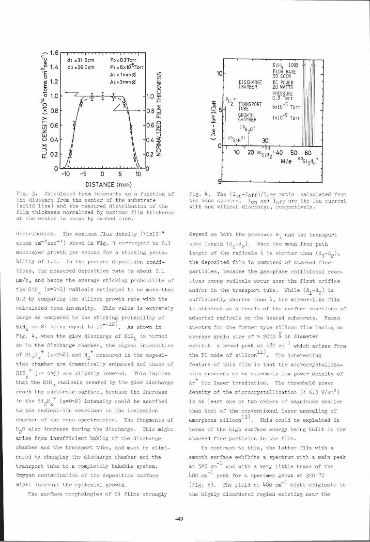
t.,, rrh^h *^a olnr^r dicnharog Of SiH, iS tUfnedr Iei. I r Wllsll Uf,I! blvw urrvf,rqr - .*
on in the d.ischarge chamber, the si-gnal intensities++
o1' S1..,ll_- (x=O'tU) and H., measured in the deposi-tx Ition chamber are dramatically enhanced. and those of
+SiH-_ (x= Qn)) are slightly lowered.. This implies-J!
that the SiH- radicals created. by the glow d.ischarge
reach the ,,rl=t"at" surface, because the i-ncreaseI
in the Si.H_-' (x=O,r"B) intensity could be ascribed.zxto the rad.ical-ion reactions in the ionizationchamber of the mass spectrometer. The fragments ofH O elso inoy.ee^^ r.---'*- +L^ iicnharo.o Thic m.iohflrDv a! DU fllur uaDs uuf 1116 UIIS Uruul llll-til] U
arise from insufficient baking of the d.ischarge
chamber and the transport tube, and. must be elimi-na.ted hv eha.np''jnB'the diseha.rse chamber and. thetransport tube to a completely bakable system.
Oxve'en eontami nation of the denosi ti on srrrfnns
might interupt the epitaxial growth.
The surface morphologies of Si fil-ns strongly
Fig. l+. The (Ion-Ioff)/fo19 ratio calcul-ated fromthe mass spectra. To' and Io11 are the ion currentwith and without discharge, respectively.
donanzl nn lrnlL fho nrocqrrno P and the trensngll,u f f
a]lu ulrs uaarlDIJ
tube length (a.-a.). When the mean free path' L Z'I ono*h nf f l.ro -ad_iCalS L iS Shorter than (a_ -A _ ) -rsrr6 urr vf /\ r u ofivf vur urrarr \ *f -*2 / ,
*lra rlannoi*azr filrn is comnosed of stacked. fine_
particles, because the gas-phase coll-isional reac-tions among radicals occur near the first orificeand/or in the transport tube. White (a.,-ao) lssrrffir,ientlw qhorter thnn ) the *it"or-like fifmurrerr /tt u
is obtained. as a result of the surface reactions ofadsorbed rad,icals on the heated. substrate. Raman
spectra for the former type silicon fil-m having an
average grain size of tu 2O0O A in d.iameterf
exhibit a broad peak at )+BO cm-' which arises from
the TO mode of "ili"onll). The interestingfeature of this fil-m is that the microcrystal-liza-tion proceeds at an extremely low power density of
f
Ar ion laser irrad-iation. The threshold power
rlanciirr nf f ho mi nrnnrrrcf ol I i z-+-'^- | z (. c t.t /. 2tJ--*-*'-at]on \< b.3 w/cm-)
is at least one or two orders of magnitud.e smalfer
than that of the conventional l-aser annealing ofamorphous
"i1i"orr13). This coul-d. be explained interms of t.he hieh surface energv treinp hri'lf, in thevv 4lrb
stacked fine particles in the film.fn contrast to this, the latter film with a
smooth surface exhibits a spectrum with a main peak-1at 52O cm - and with a very littl-e trace of the
I ^^ -l ^^^ 6^4OU cm peaK lor a speclmen grown al JUU -u/-.
-\ . l
^^ -]-(Fie. ,). The yie]d. at 4U0 cm - might originate in
tlra hr'rlr-l rr .li o^7.dored rooi nn ewi etino neer thcullg rrISIlfJ ui DUf uvr uu r u6f ufi u^r u vrrrb rrvur
l9oU!(\
.E(,oEoo
.tox
Fu)ztlJox=JL
o
bI
5
r/)alrlzx(J-FJ|IotrlN
=Eoz2
siH4 100u
5bo$,8fi"DISCHARGE DC POl,lERCHAMBER 20 WATTS
2u + ElSr?8FF"2 IRANSP0RT 6xl0-5 TorrTUBE
GR0WTH lxl0-5 TorrCHAl]BER
t trro*
t'siH'* | so
10 2o :osiHz* oo"r"uo.oj:r_-
449

(DFzf,tl.J
l-Jl,!lE
F(/)zt!Fzz
E
Ar' LASER^( 5115 A )10.0 W/cmt n
SJBSTRATETEMPERATURE('c )
fitms is not observed. Figure 6 shows the RHEED
pattern of a film grown on a si(roo) substrate at a
temperature of 6OO oC. The photograph ind-icates
that the silicon epitaxial growth occurs at 600 oc
by the use of SiH* rad-ical beam' Further decrease
of the epitaxial temperature would be possibfe vhen
the oxwsen eontamination in the bearn is eliminated-.U ar v vJ!t,
g)+. Conclusions
Siliconthin-filmsoncrysta]-lineSisubstratehave been grown in the temperature range from
3OO oC to 5oo oc by using rad-ical beam deposition
technique. The fihns grown at temperatures below
500 oC are preferentially oriented to the same
direction as the substrate, while at a temperature
of 5oO oC the epitaxial growbh occurs on Sj-(rOO)
surface.
Acknowled-gPent s
The authors wish to thank T' Abe of AYUMI In-
d-ustry Co. Ltd,. for constructing the RBD system and
Y. Kuwano and N. Nakamura of SANYO Etectric Co' Ltd''
for RHEED measurements.
Referenc e s
l) J.E.Davey and T.Pankey, J.Appl'Phys' 39 (rg68)
l-941.
2) L.L.Chang, L.Esaki, W.E'Howard and R'Ludeke'J.Vac.Sci.Technol. 10 (l-glZ) rf.
3) Y.Shiraki, Y.Katayama, K'L'T'Kobayashi and"
K.F.Komatsubara, J.cryst'Growbh I+5 (rgf8) 2BT'
)+) Y.ota, J.Appl.Phys.5r (rg8o) rroe'
,) M.Matsui, Y.Shiraki and E'Maruyama, J'Appl'Phys'52 (]_g9z) gg5.
6) P.C.Zalm and L.J.Becker, Appl'Phys'Lett' l+l
(rqae) r5T.
7 ) T. Takagi , I.Yamad'a and A' Sasaki , J 'Vac ' Sci 'Technol. 12 (tgt>) 11zB.
B) R.P.H.Chang and S.Darack, Appl'Phys'Lett' h2
(rg8s) 272.
T.J.Donahue, W.R.Burger and R'Reif , Appl'Phys'Lett . IIr (rg8\ ) :h5.
fO) T.Hariu, K.Matsushita, Y'Komatsu, S'Shibuya'S.Igarashi and Y.Shibata, Inst'Phys'Conf'Ser'6, (:-g1z) r\r.
1l-) M.Hirose, S.Miyazaki and H'Hirata, Pv'oc' Bth
SUmp.on ISIAT' Tokyo (1'984) 2L3'
12 ) B.A. Joyce and R. R.Bradley, Phil'Mag' 1)+ 11966)
289.
13) J.S.Witfiams, W.L.Bror'rno H'J'Leamy, J'M'Poate'J.W.Rod-gers, D.Rousseau, G'A'Rozgoni, J:A'Shelnand T.T.Sheng, Appl.Phys.Lett' 33 (rqf8) >\z'
600
Fig. 5. Raman
500 and 6oo "cthat for c-Si
Fig. 6. RHEED Patterns offitm deposited on Si(fOO)d,irection of the incid-ent
5,60 520 480 tAo 400
WAVENUMBER ( cm -1 )
spectra for films grown at 300, l+00,
ritf, mirror-like morphologies and
substrate as a reference.
tuf 500 i tt i"tn siliconsubstrate at 600 oC. The
electron beam is <l-00>.
interface between the d-eposition layer and sub-
strate as a consequence of incomplete cleaning of
the substrate prior to the d-eposition and some
oxygen contamination involved in the radical beam'
The whole spectrum is kept unchanged even with
laser irrad.iation at a power density of 28 Wf cmz.
Polarization effect of the Raman intensity at 52O
"*-l fo, the speci_men grovn on a si(roo) substrate
even at temperatures of 300, )+OO and 500 oC ind'i-
cated that the film is preferentially.oriented to
the same direction as the =ubstr"ttll) ' As shown
in Fig. !, the Raman spectra of the fllms grown at
substrate temperatures above 500 oC is essentially
id.enticaftothatofacrysta].]-ineSisubstrateand-ttfre )+BO
"r-t p..k due to d.isord"ered- reglons in the