Photolithography-based realization of Frequency Steerable...
19
Photolithography-based realization of Frequency Steerable Acoustic Sensors on PVDF substrate E. Baravelli 1 , L. De Marchi 2 , M. Ruzzene 1 , N. Speciale 2 1 School of Aerospace Engineering, GeorgiaTech 2 University of Bologna – MAS group
Transcript of Photolithography-based realization of Frequency Steerable...
Photolithography-based
realization of Frequency
Steerable Acoustic Sensors
on PVDF substrate
E. Baravelli1, L. De Marchi2, M. Ruzzene1, N. Speciale2
1School of Aerospace Engineering, GeorgiaTech
2University of Bologna – MAS group
2
Outline
■ Guided-wave based directional sensing
■ Frequency Steerable Acoustic Transducers
(FSATs)
■ FSAT fabrication
■ Experiments
■ Conclusions
3
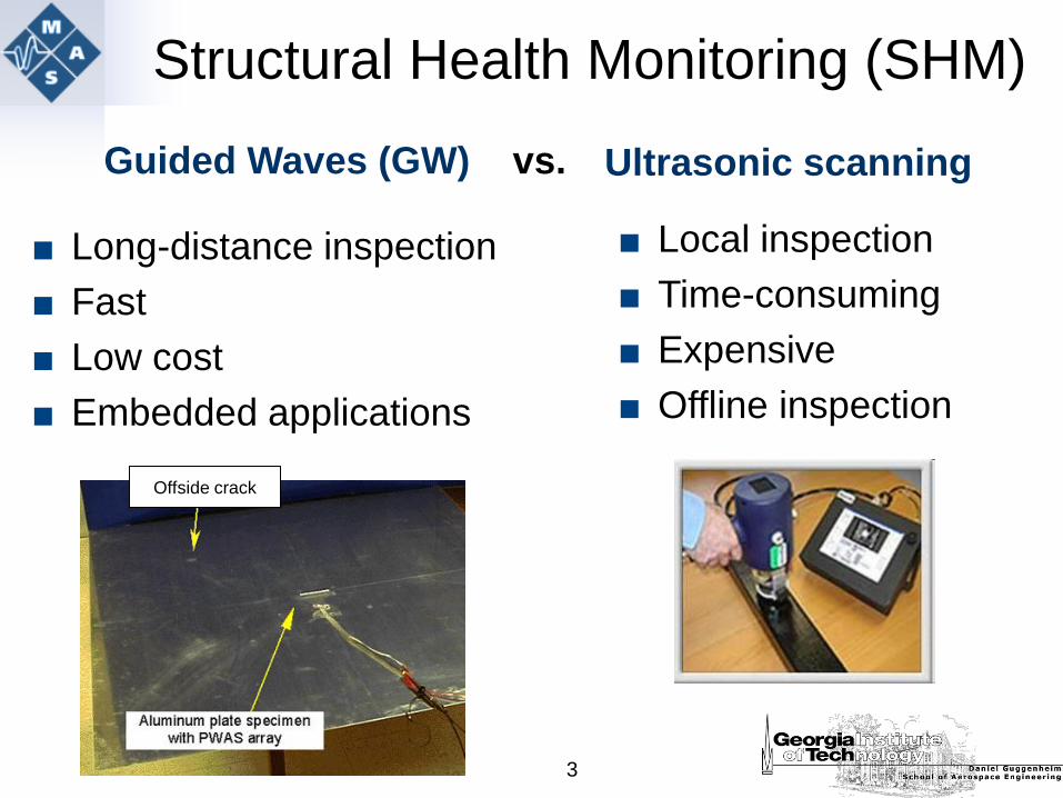
Structural Health Monitoring (SHM)
■ Long-distance inspection
■ Fast
■ Low cost
■ Embedded applications
■ Local inspection
■ Time-consuming
■ Expensive
■ Offline inspection
Guided Waves (GW) vs. Ultrasonic scanning
Offside crack
4
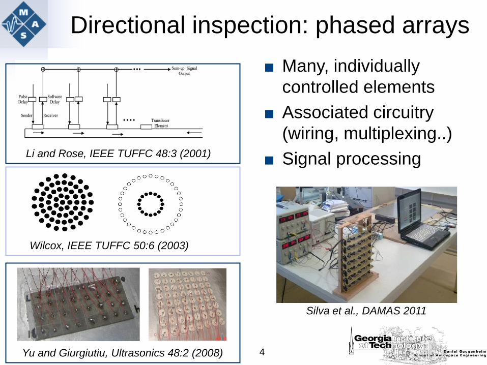
Directional inspection: phased arrays
Yu and Giurgiutiu, Ultrasonics 48:2 (2008)
Wilcox, IEEE TUFFC 50:6 (2003)
Li and Rose, IEEE TUFFC 48:3 (2001)
■ Many, individually
controlled elements
■ Associated circuitry
(wiring, multiplexing..)
■ Signal processing
Silva et al., DAMAS 2011
5
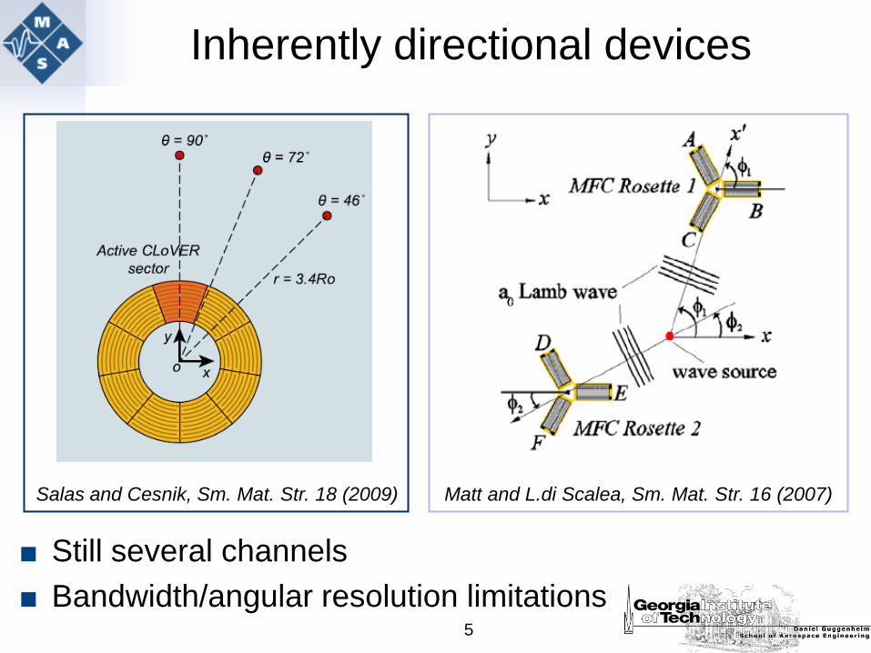
Inherently directional devices
Salas and Cesnik, Sm. Mat. Str. 18 (2009)
■ Still several channels
■ Bandwidth/angular resolution limitations
Matt and L.di Scalea, Sm. Mat. Str. 16 (2007)
6
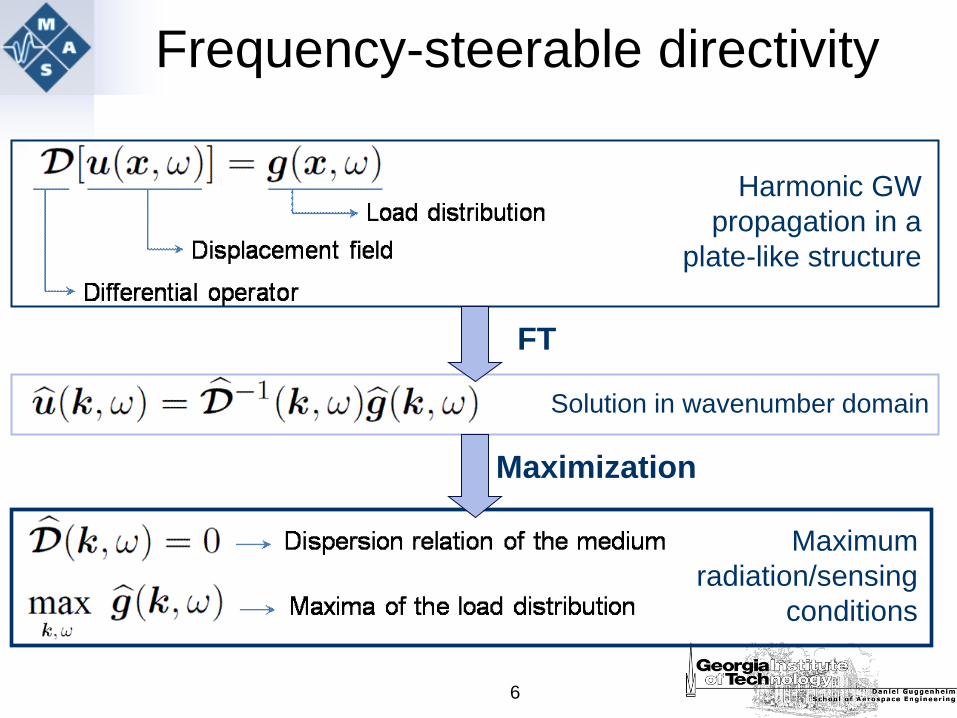
Frequency-steerable directivity
Harmonic GW
propagation in a
plate-like structure
Solution in wavenumber domain
FT
Maximization
Maximum
radiation/sensing
conditions
7
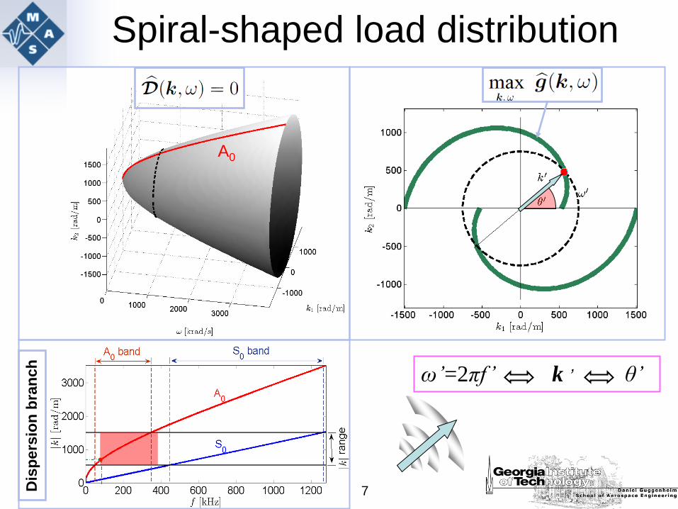
Spiral-shaped load distribution
A0
Dis
pers
ion
bra
nch
ω’=2πf’ k ’ θ’
8
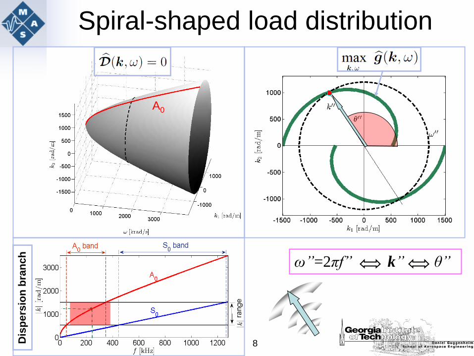
Spiral-shaped load distribution
A0
Dis
pers
ion
bra
nch
ω”=2πf” k” θ”
9
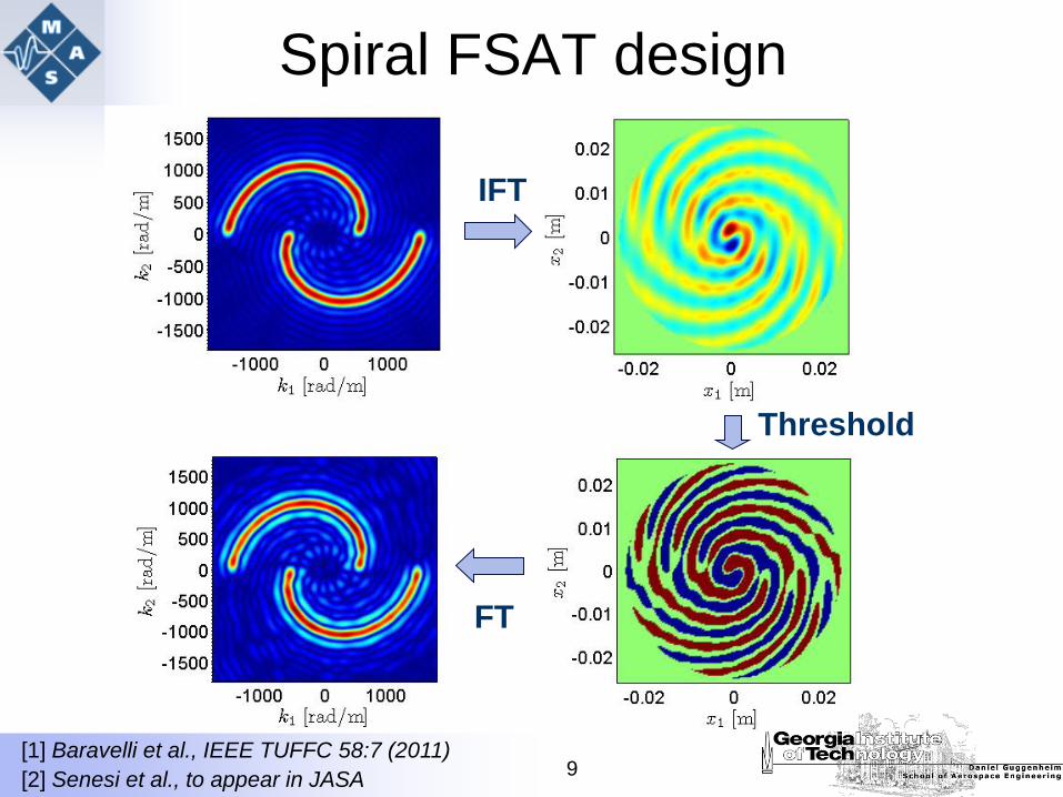
Spiral FSAT design
Threshold
IFT
FT
[1] Baravelli et al., IEEE TUFFC 58:7 (2011)
[2] Senesi et al., to appear in JASA
10
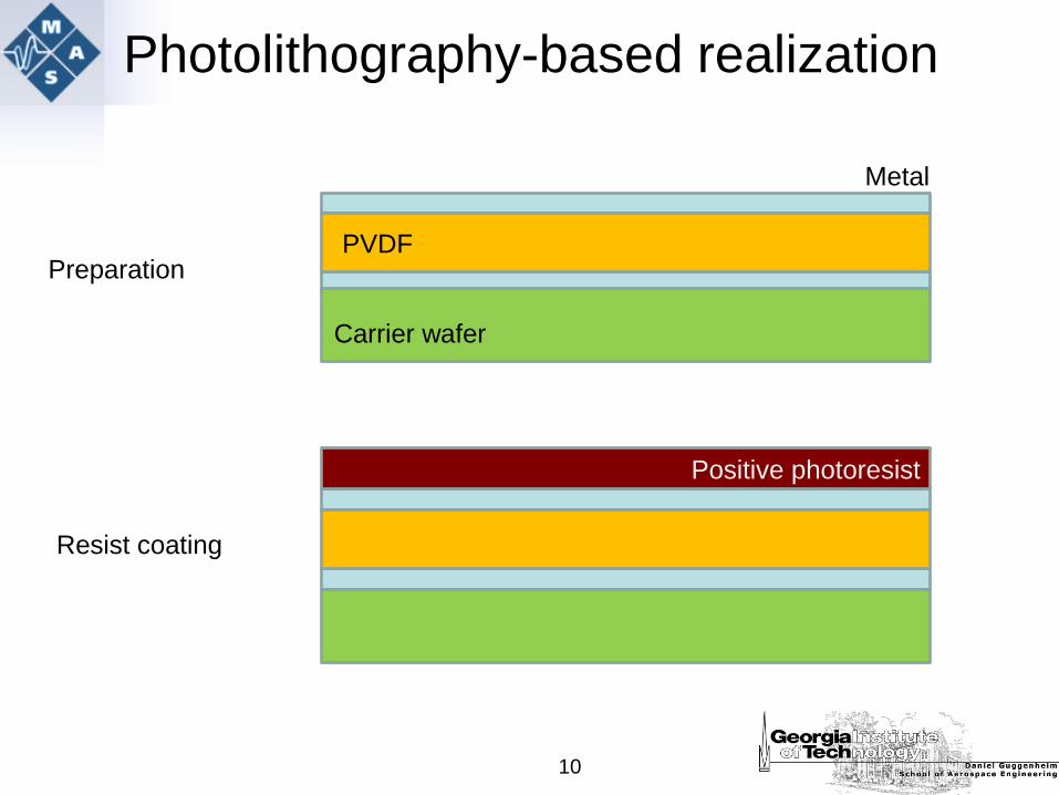
Photolithography-based realization
Preparation
Resist coating
Carrier wafer
PVDF
Metal
Positive photoresist
11
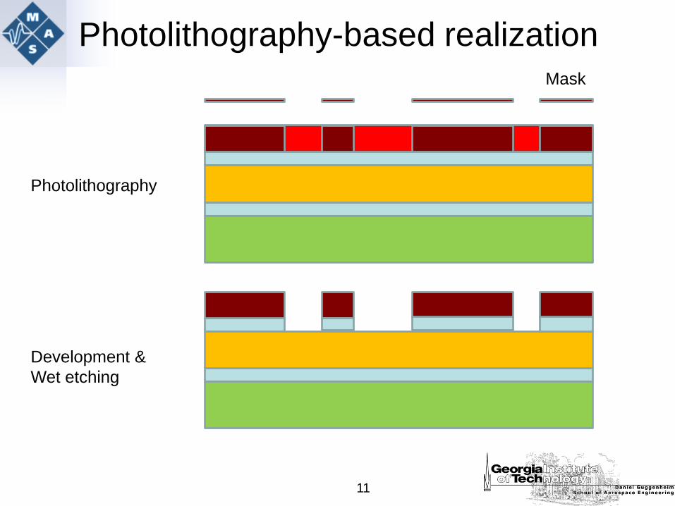
Photolithography-based realization
Photolithography
Development &
Wet etching
Mask
12
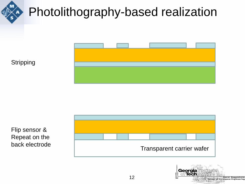
Stripping
Flip sensor &
Repeat on the
back electrode wafer Transparent carrier wafer
Photolithography-based realization
13
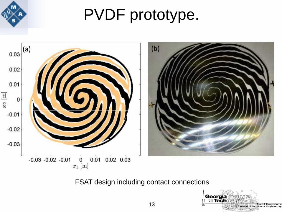
PVDF prototype.
FSAT design including contact connections
14
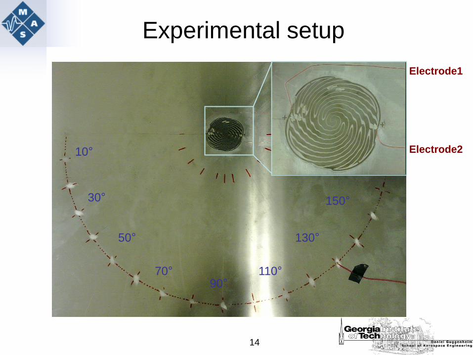
Experimental setup
10°
30°
170°
50° 130°
90° 110° 70°
150°
Electrode1
Electrode2
15
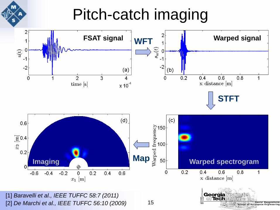
Pitch-catch imaging
STFT
WFT
Map
FSAT signal Warped signal
Warped spectrogram Imaging
[1] Baravelli et al., IEEE TUFFC 58:7 (2011)
[2] De Marchi et al., IEEE TUFFC 56:10 (2009)
16
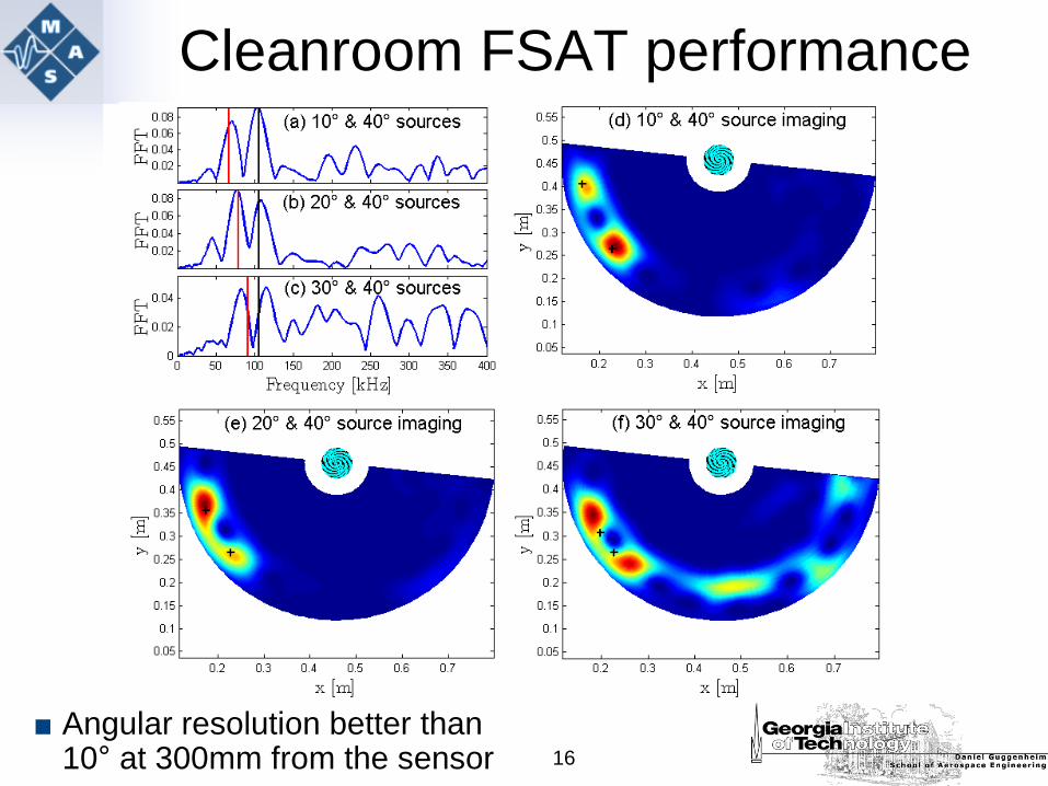
Cleanroom FSAT performance
■ Angular resolution better than 10° at 300mm from the sensor
17
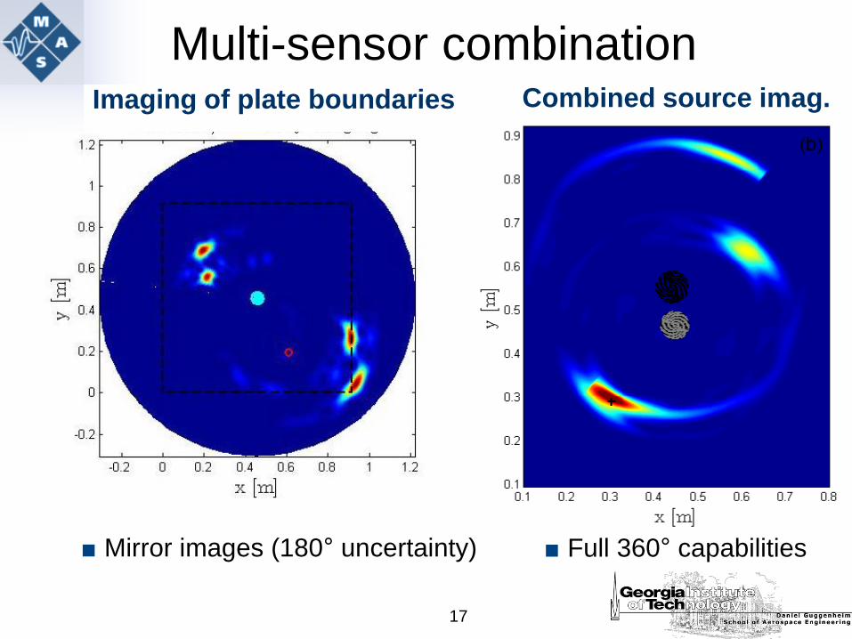
Multi-sensor combination
■ Mirror images (180° uncertainty) ■ Full 360° capabilities
Imaging of plate boundaries Combined source imag.
18
Conclusions
■ FSAT geometry provides spatial filtering and hence
directional sensing
■ 2D imaging with a single FSAT signal
■ Photolithography fabrication on PVDF
■ Low hardware & software complexity enable in-situ and
wireless SHM
19
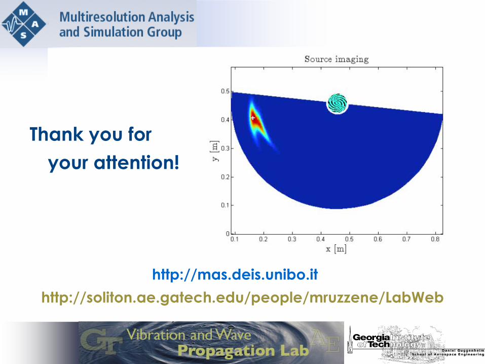
Thank you for
your attention!
http://mas.deis.unibo.it
http://soliton.ae.gatech.edu/people/mruzzene/LabWeb