Photolithography with a Photolithography with a...
113
Photolithography with a Twist Photolithography with a Photolithography with a Twist Twist Martin Afromowitz Professor of Electrical Engineering University of Washington Presenter: A workshop on gray scale and 3-D methods
Transcript of Photolithography with a Photolithography with a...
Photolithography with a TwistPhotolithography with a Photolithography with a TwistTwist
Martin AfromowitzProfessor of Electrical EngineeringUniversity of Washington
Presenter:
A workshop on gray scale and 3-D methods
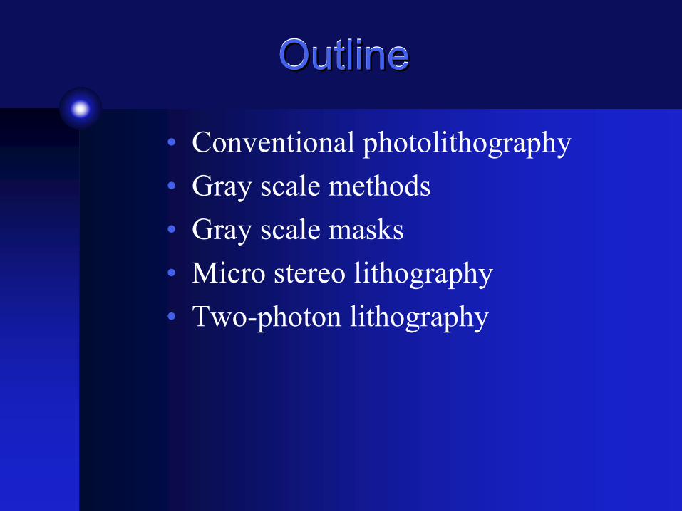
OutlineOutlineOutline
• Conventional photolithography• Gray scale methods• Gray scale masks• Micro stereo lithography• Two-photon lithography
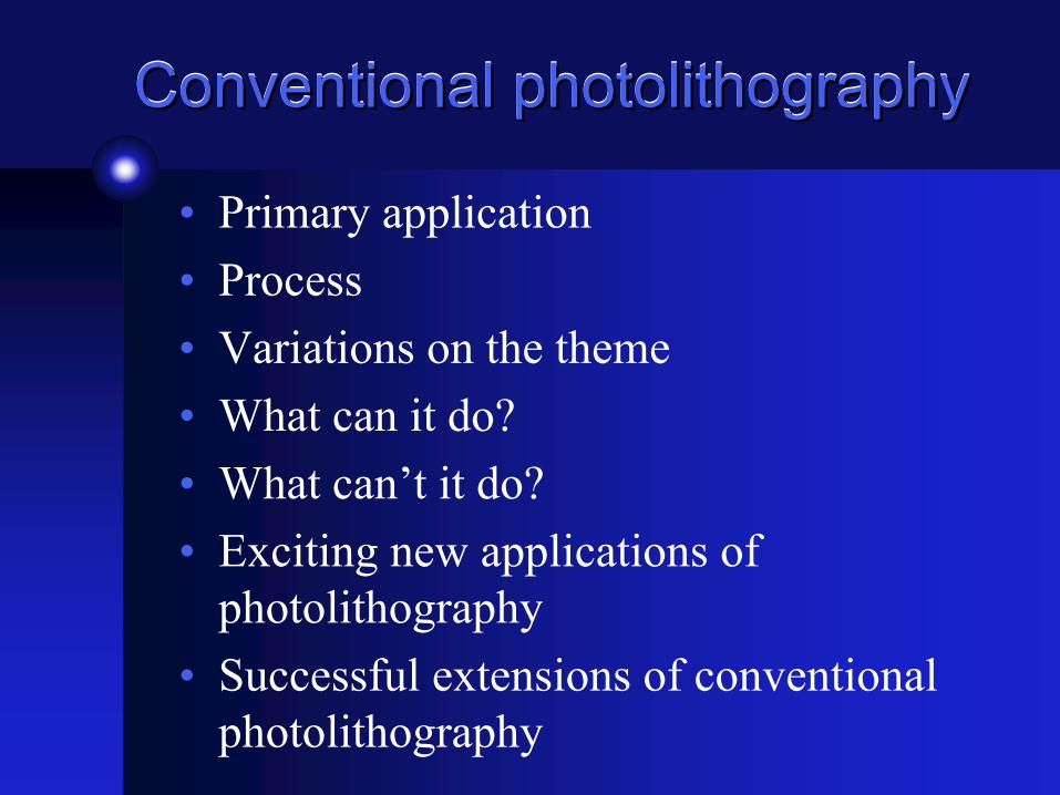
Conventional photolithographyConventional photolithographyConventional photolithography
• Primary application• Process• Variations on the theme• What can it do?• What can’t it do?• Exciting new applications of
photolithography• Successful extensions of conventional
photolithography
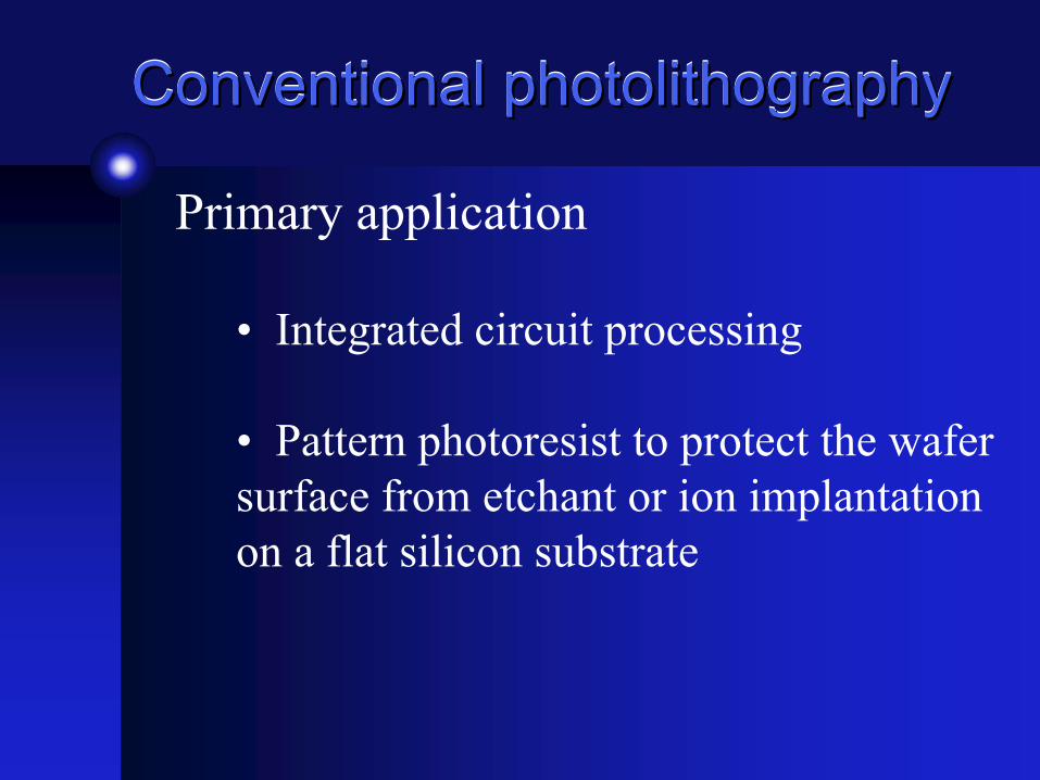
Conventional photolithographyConventional photolithographyConventional photolithography
Primary application
• Integrated circuit processing
• Pattern photoresist to protect the wafer surface from etchant or ion implantation on a flat silicon substrate
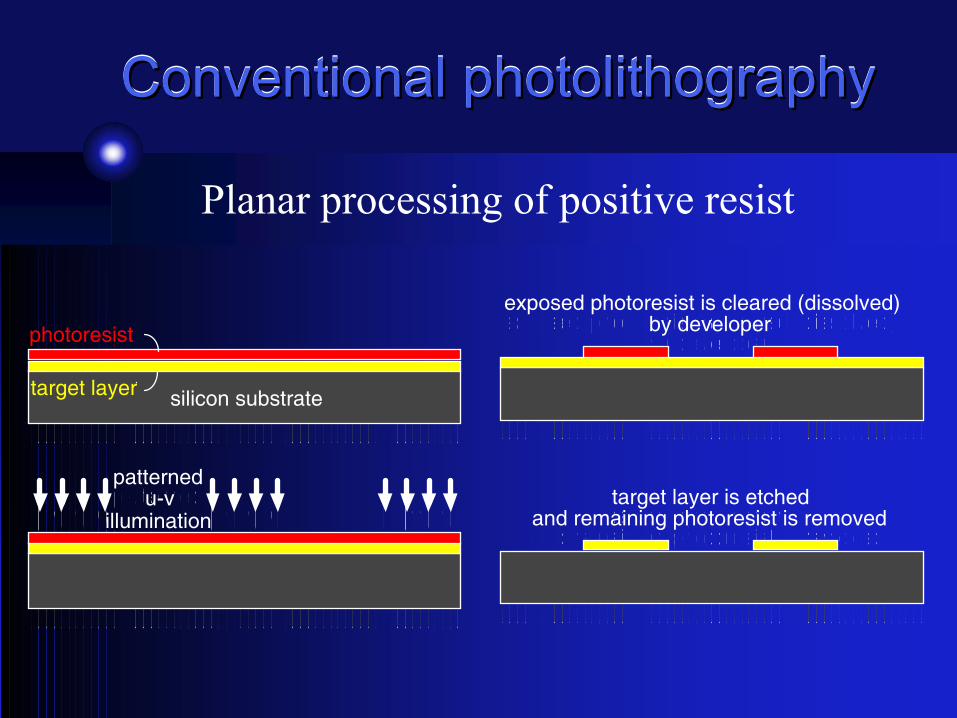
Conventional photolithographyConventional photolithographyConventional photolithography
Planar processing of positive resist
silicon substratetarget layer
photoresist
patternedu-v
illumination
exposed photoresist is cleared (dissolved)by developer
target layer is etched and remaining photoresist is removed
silicon substratetarget layer
photoresist
patternedu-v
illumination
exposed photoresist is cleared (dissolved)by developer
target layer is etched and remaining photoresist is removed
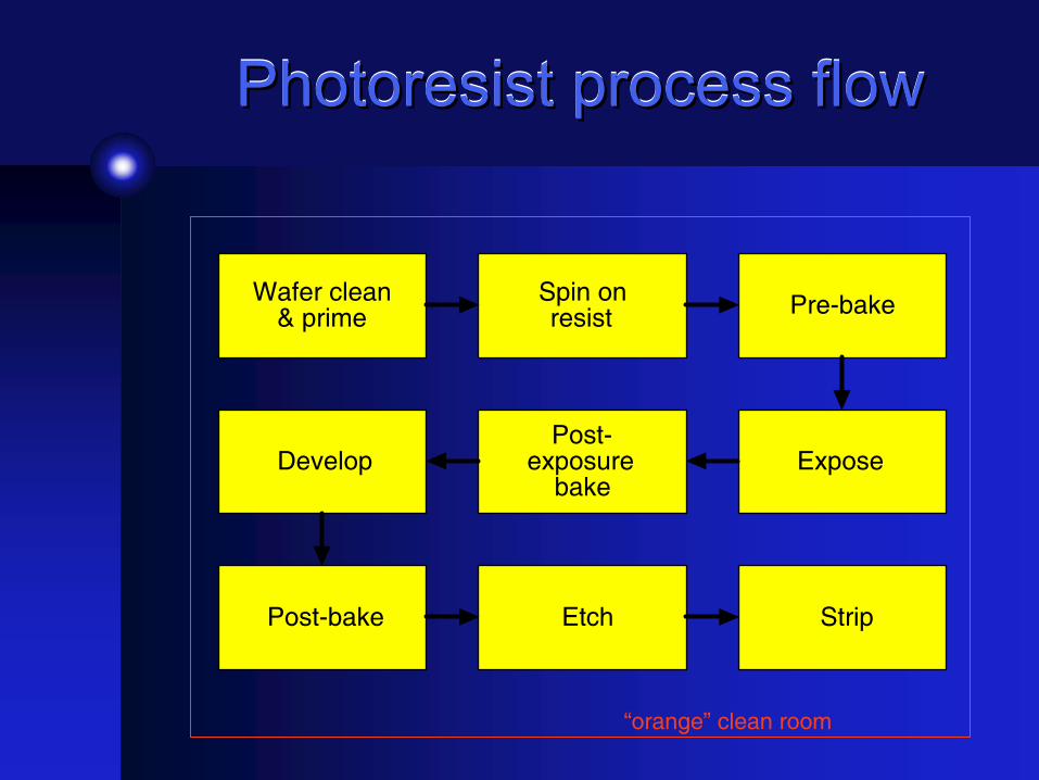
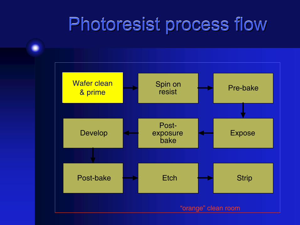
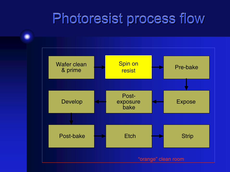
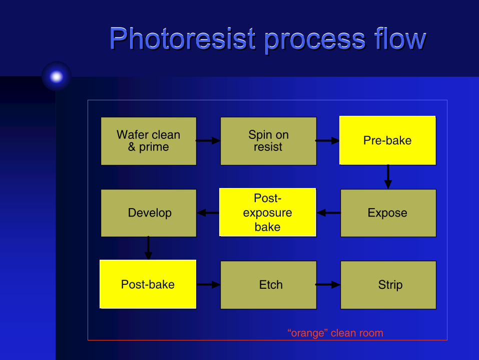
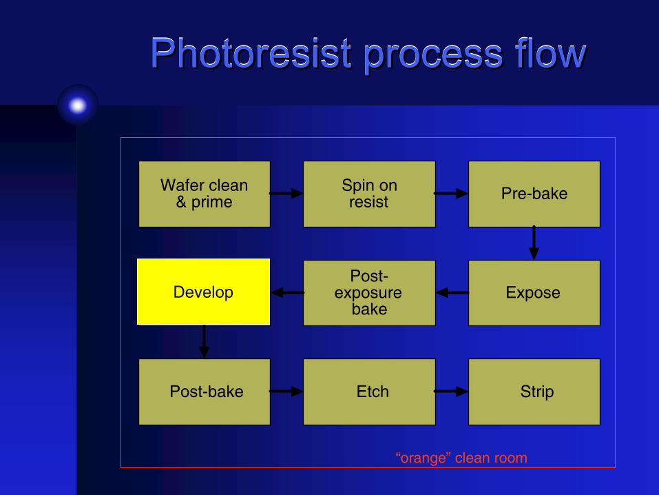
Photoresist process flowPhotoresist process flowPhotoresist process flow
Wafer clean& prime
Spin onresist Pre-bake
ExposePost-
exposurebake
Develop
Post-bake Etch Strip
“orange” clean room
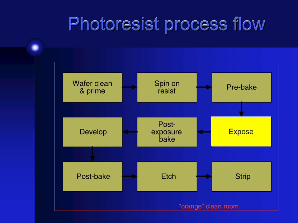
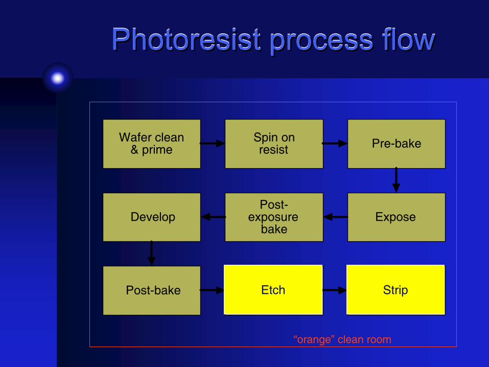
Photoresist process flowPhotoresist process flowPhotoresist process flow
Wafer clean& prime
Spin onresist Pre-bake
ExposePost-
exposurebake
Develop
Post-bake Etch Strip
“orange” clean room
Wafer clean& prime
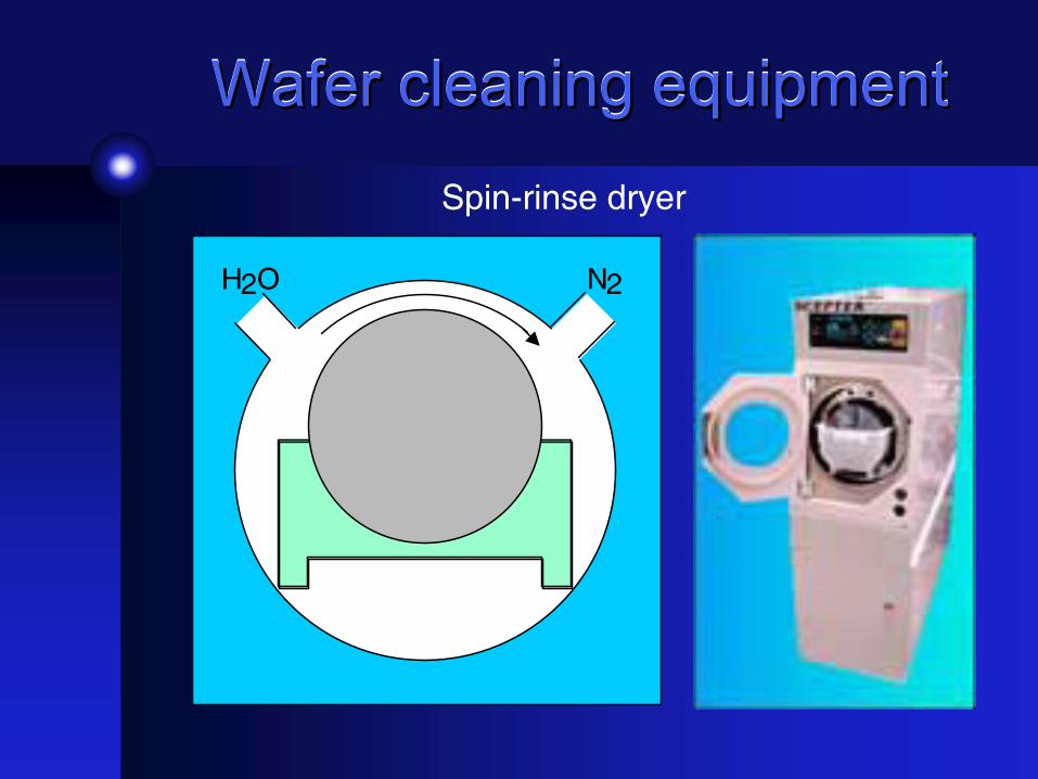
Wafer cleaning equipmentWafer cleaning equipmentWafer cleaning equipment
H2O N2
Spin-rinse dryer
Photoresist process flowPhotoresist process flowPhotoresist process flow
Wafer clean& prime
Spin onresist Pre-bake
ExposePost-
exposurebake
Develop
Post-bake Etch Strip
“orange” clean room
Spin onresist
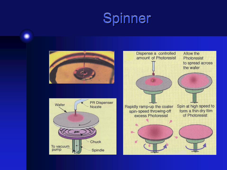
SpinnerSpinnerSpinner
Photoresist process flowPhotoresist process flowPhotoresist process flow
Wafer clean& prime
Spin onresist Pre-bake
ExposePost-
exposurebake
Develop
Post-bake Etch Strip
“orange” clean room
Pre-bake
Post-exposure
bake
Post-bake
Photoresist process flowPhotoresist process flowPhotoresist process flow
Wafer clean& prime
Spin onresist Pre-bake
ExposePost-
exposurebake
Develop
Post-bake Etch Strip
“orange” clean room
Expose
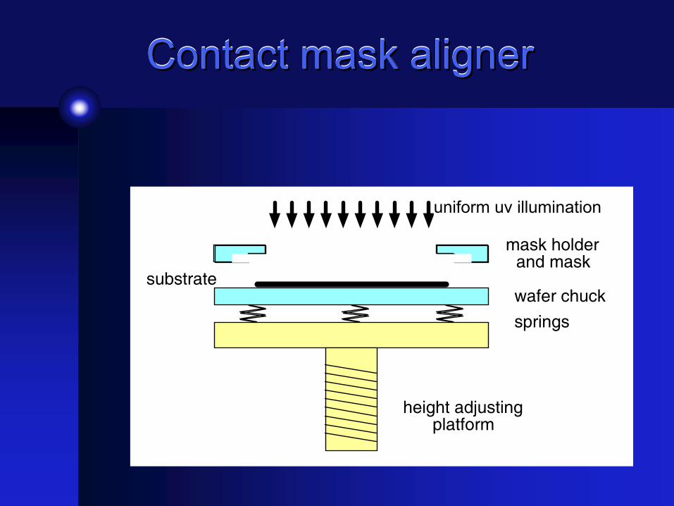
Contact mask alignerContact mask alignerContact mask aligner
height adjustingplatform
springs
wafer chucksubstrate
mask holderand mask
uniform uv illluminationuniform uv illumination
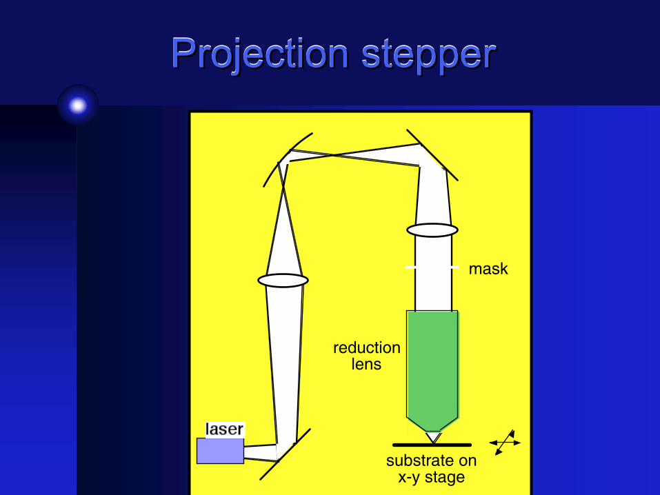
Projection stepperProjection stepperProjection stepper
mask
reductionlens
substrate onx-y stage
Photoresist process flowPhotoresist process flowPhotoresist process flow
Wafer clean& prime
Spin onresist Pre-bake
ExposePost-
exposurebake
Develop
Post-bake Etch Strip
“orange” clean room
Develop
Photoresist process flowPhotoresist process flowPhotoresist process flow
Wafer clean& prime
Spin onresist Pre-bake
ExposePost-
exposurebake
Develop
Post-bake Etch Strip
“orange” clean room
Etch Strip
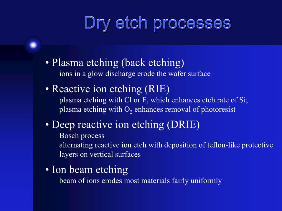
Dry etch processesDry etch processesDry etch processes
• Plasma etching (back etching)ions in a glow discharge erode the wafer surface
• Reactive ion etching (RIE)plasma etching with Cl or F, which enhances etch rate of Si;plasma etching with O2 enhances removal of photoresist
• Deep reactive ion etching (DRIE)Bosch processalternating reactive ion etch with deposition of teflon-like protective layers on vertical surfaces
• Ion beam etchingbeam of ions erodes most materials fairly uniformly
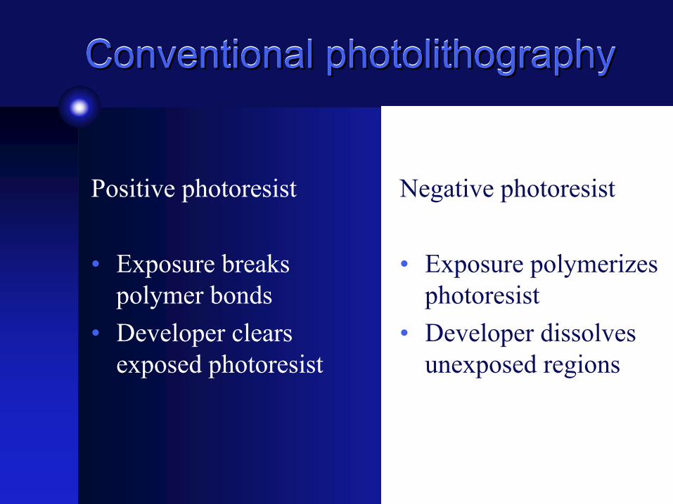
Conventional photolithographyConventional photolithographyConventional photolithography
Positive photoresist
• Exposure breaks polymer bonds
• Developer clears exposed photoresist
Negative photoresist
• Exposure polymerizes photoresist
• Developer dissolves unexposed regions
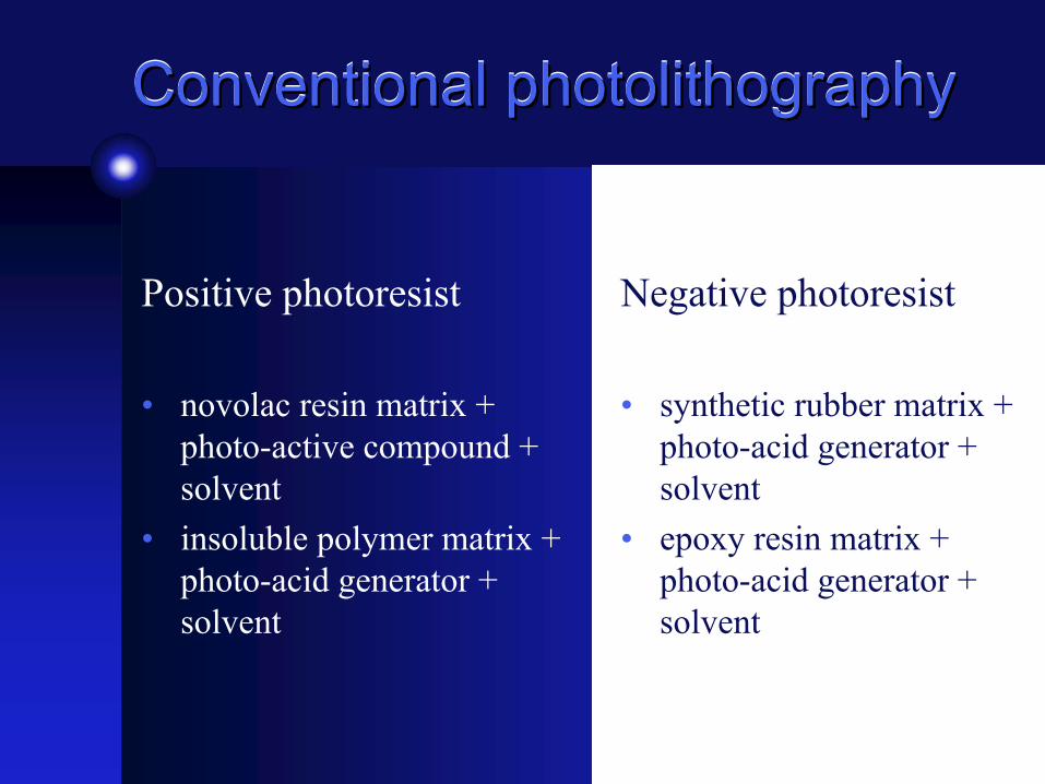
Conventional photolithographyConventional photolithographyConventional photolithography
Positive photoresist
• novolac resin matrix + photo-active compound + solvent
• insoluble polymer matrix + photo-acid generator + solvent
Negative photoresist
• synthetic rubber matrix + photo-acid generator + solvent
• epoxy resin matrix + photo-acid generator + solvent
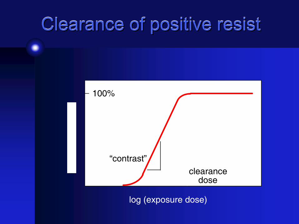
Clearance of positive resistClearance of positive resistClearance of positive resist
log (exposure dose)
100%
clearancedose
“contrast”
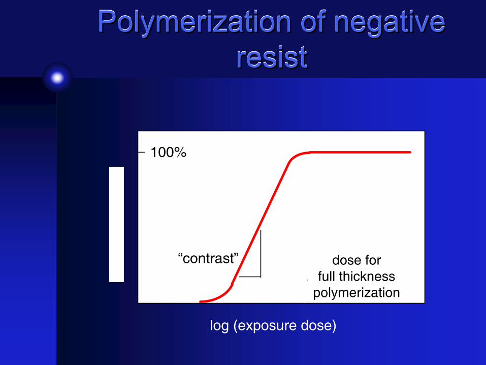
Polymerization of negative resist
Polymerization of negative Polymerization of negative resistresist
log (exposure dose)
100%
clearancedose
“contrast” dose forfull thickness
polymerization
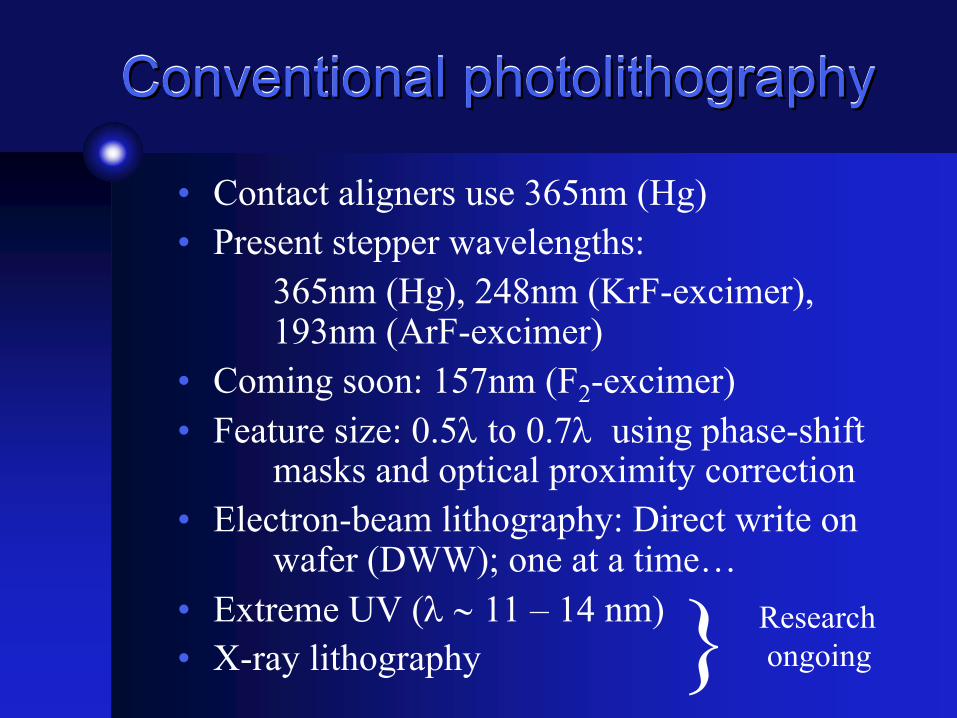
Conventional photolithographyConventional photolithographyConventional photolithography
• Contact aligners use 365nm (Hg)• Present stepper wavelengths:
365nm (Hg), 248nm (KrF-excimer), 193nm (ArF-excimer)
• Coming soon: 157nm (F2-excimer)• Feature size: 0.5λ to 0.7λ using phase-shift
masks and optical proximity correction• Electron-beam lithography: Direct write on
wafer (DWW); one at a time…• Extreme UV (λ ∼ 11 – 14 nm)• X-ray lithography } Research
ongoing
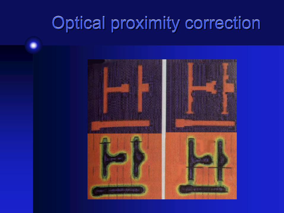
Optical proximity correctionOptical proximity correctionOptical proximity correction
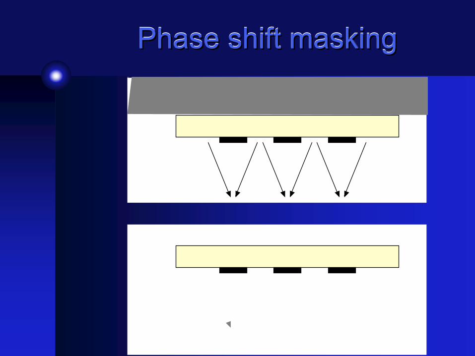
Phase shift maskingPhase shift maskingPhase shift masking
mask
chrome
diffraction
180° phaseshifter
destructive interference
coherent light from excimer laser source
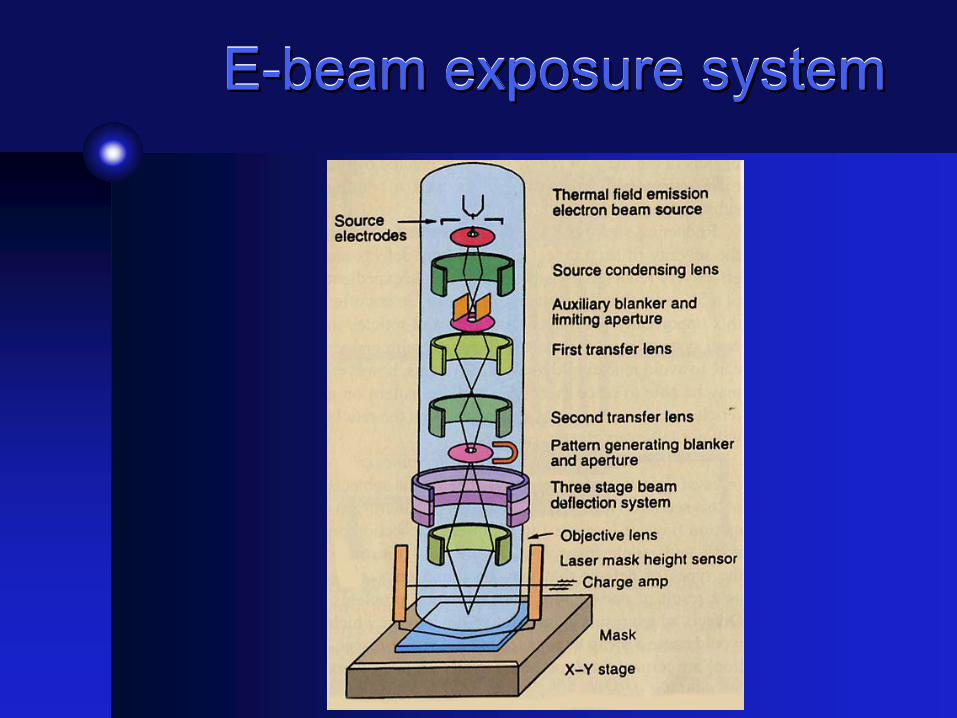
E-beam exposure systemEE--beam exposure systembeam exposure system
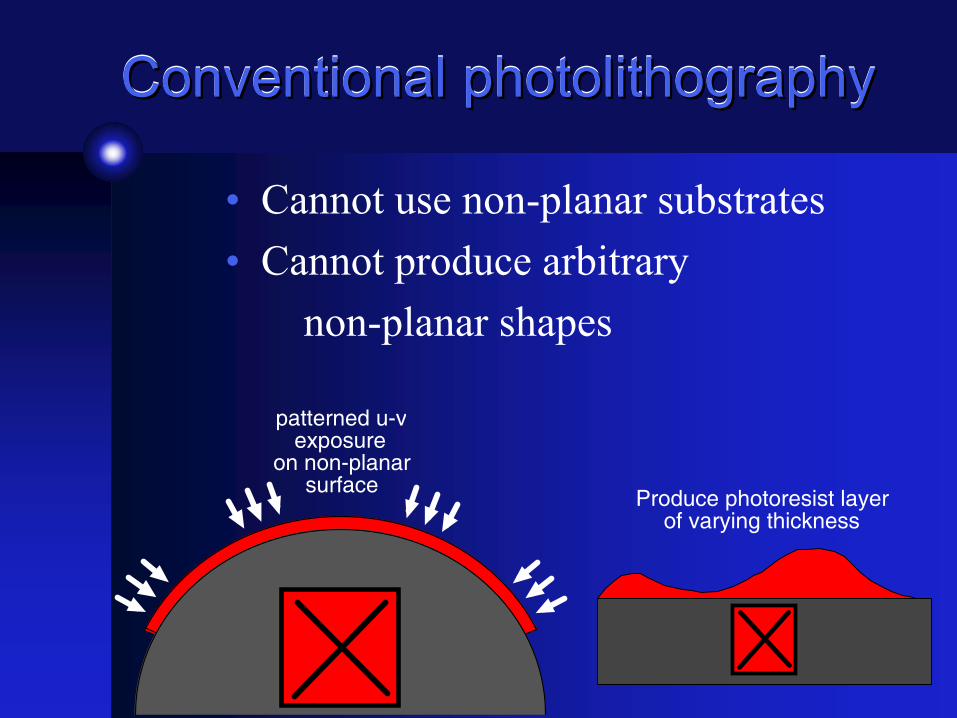
Conventional photolithographyConventional photolithographyConventional photolithography
• Cannot use non-planar substrates• Cannot produce arbitrary
non-planar shapes
patterned u-vexposure
on non-planarsurface
Produce photoresist layerof varying thickness
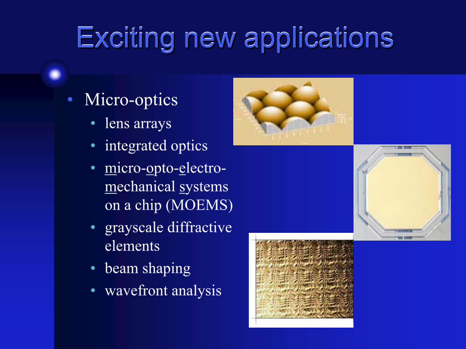
Exciting new applicationsExciting new applicationsExciting new applications
• Micro-optics• lens arrays• integrated optics• micro-opto-electro-
mechanical systems on a chip (MOEMS)
• grayscale diffractive elements
• beam shaping• wavefront analysis
Exciting new applicationsExciting new applicationsExciting new applications
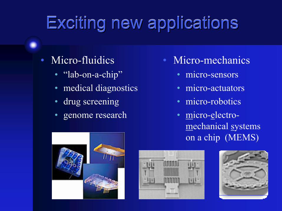
• Micro-fluidics• “lab-on-a-chip”• medical diagnostics• drug screening• genome research
• Micro-mechanics• micro-sensors• micro-actuators• micro-robotics• micro-electro-
mechanical systems on a chip (MEMS)
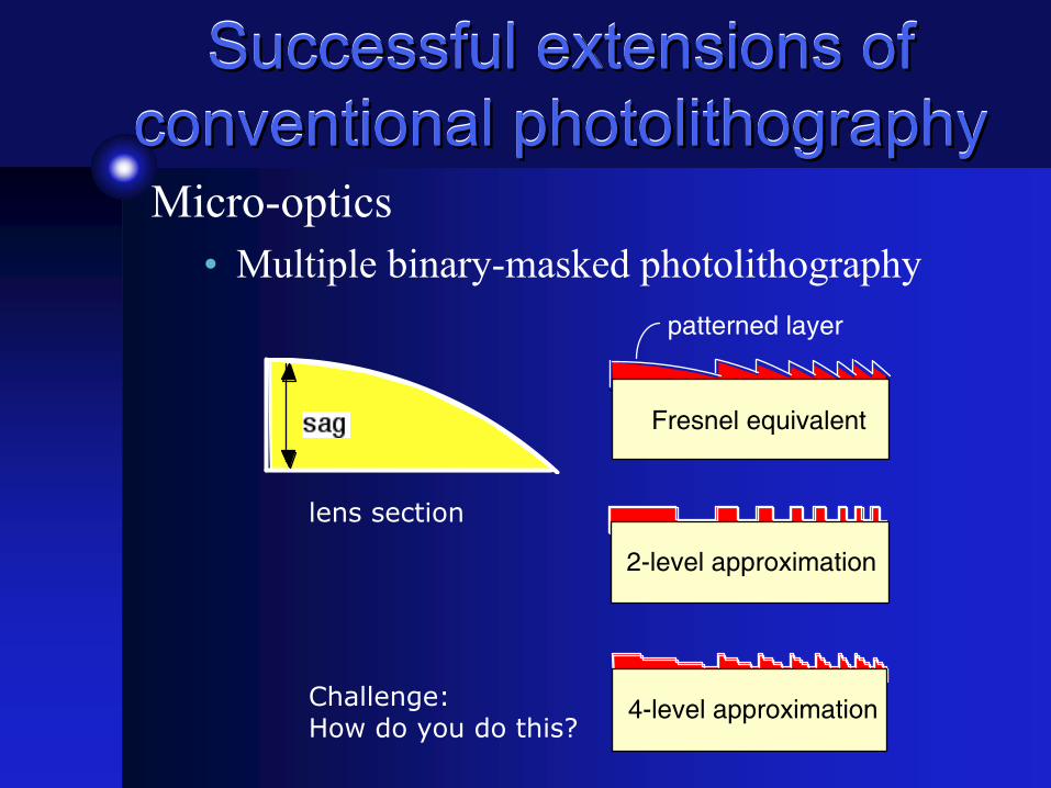
Successful extensions of conventional photolithography
Successful extensions of Successful extensions of conventional photolithographyconventional photolithographyMicro-optics
• Multiple binary-masked photolithography
Challenge:How do you do this?
patterned layer
Fresnel equivalent
2-level approximation
4-level approximation
lens section
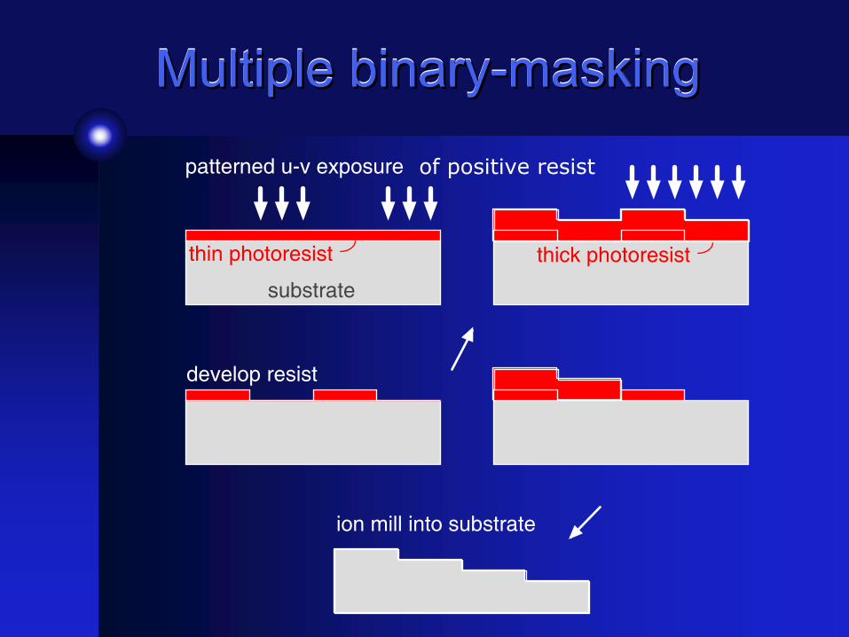
Multiple binary-maskingMultiple binaryMultiple binary--maskingmasking
patterned u-v exposure
thin photoresist
substrate
develop resist
thick photoresist
ion mill into substrate
of positive resist
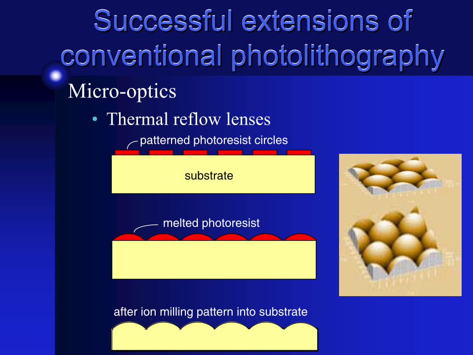
Successful extensions of conventional photolithography
Successful extensions of Successful extensions of conventional photolithographyconventional photolithographyMicro-optics
• Thermal reflow lensespatterned photoresist circles
substrate
melted photoresist
after ion milling pattern into substrate
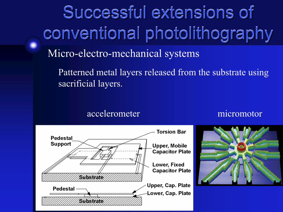
Successful extensions of conventional photolithography
Successful extensions of Successful extensions of conventional photolithographyconventional photolithographyMicro-electro-mechanical systems
Patterned metal layers released from the substrate using sacrificial layers.
accelerometer micromotor
Gray scale lithography with positive photoresist
Gray scale lithography with positive photoresist
• Advantages of gray scale• Photoresist clearance vs dose• Process flow• Examples of current applications

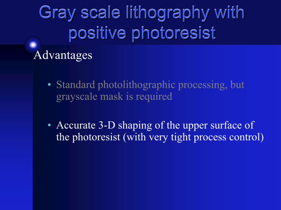
Gray scale lithography with positive photoresist
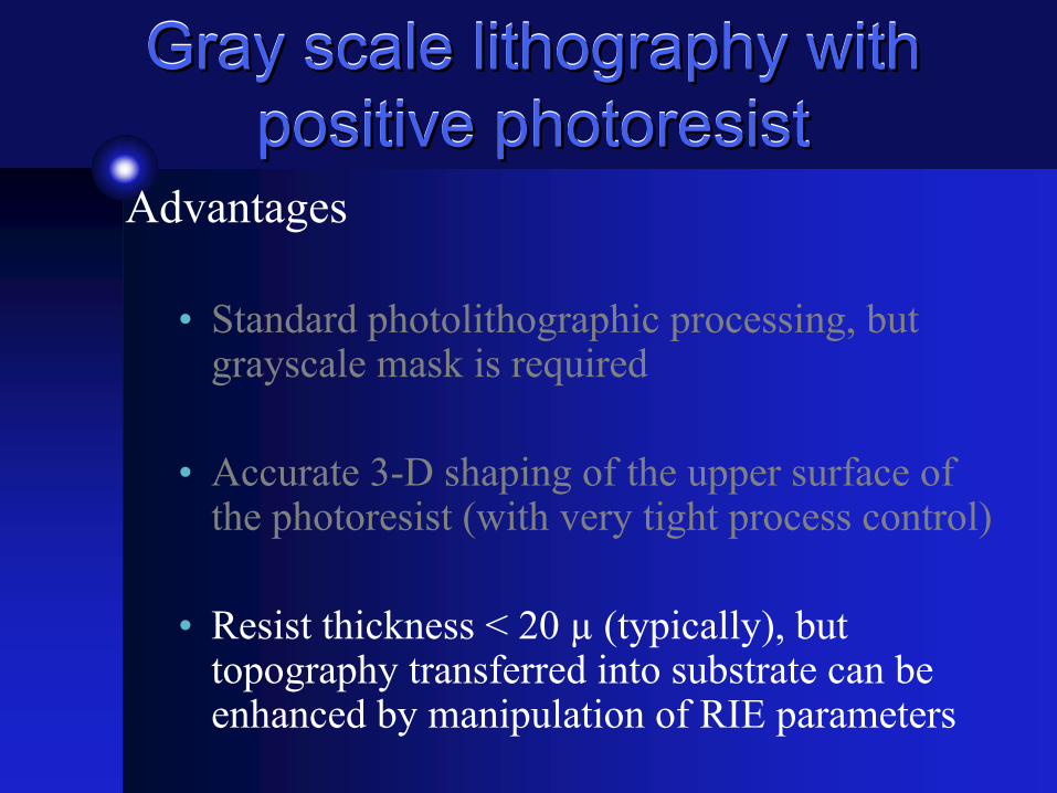
Gray scale lithography with Gray scale lithography with positive photoresistpositive photoresist
Advantages
• Standard photolithographic processing, but grayscale mask is required
Gray scale lithography with positive photoresist
Gray scale lithography with Gray scale lithography with positive photoresistpositive photoresist
Advantages
• Standard photolithographic processing, but grayscale mask is required
• Accurate 3-D shaping of the upper surface of the photoresist (with very tight process control)
• Resist thickness < 20 µ (typically), but topography transferred into substrate can be enhanced by manipulation of RIE parameters
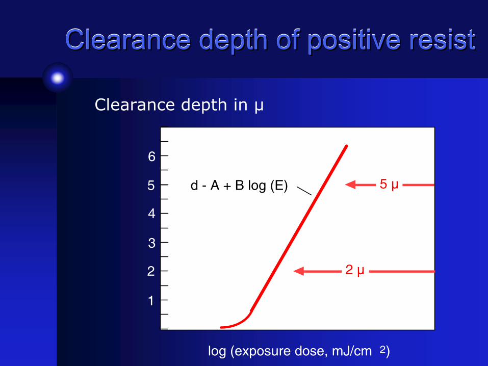
Clearance depth of positive resistClearance depth of positive resistClearance depth of positive resist
log (exposure dose, mJ/cm 2)
1
2
3
4
5
6
d A + B log (E) 5 µ
2 µ
Clearance depth in µ
Clearance depth: theoryClearance depth: theoryClearance depth: theory
Exposure Dose = E = I0 t (mJ/cm2)
I0 = Incident light flux (mW/cm2)t = Exposure time (sec)
Energy needed/cm3 to clear = W0 (mJ/cm3)
Energy absorbed per cm3 at depth x = W(x)
W(x) = α I(x) t
α = absorption coef (cm-1) fractional loss of intensity per cm
I(x) = (1–R) I0 exp(–α x)
R = reflectivity
W(x) = α (1–R) I0 t exp(–α x)
I(x)
x
I0
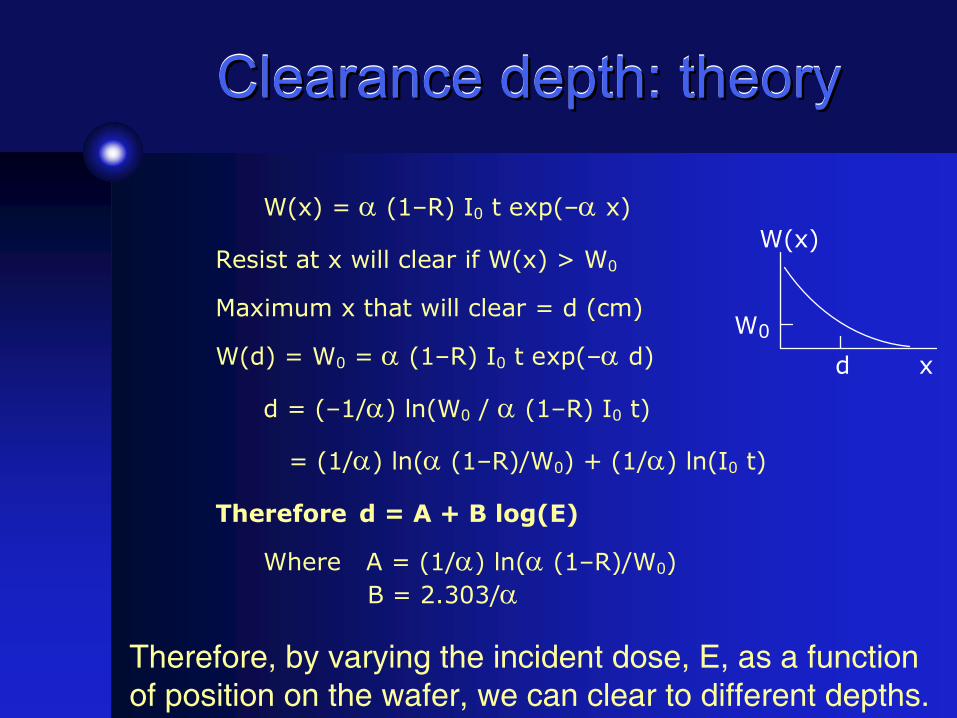
Clearance depth: theoryClearance depth: theoryClearance depth: theory
W(x) = α (1–R) I0 t exp(–α x)
Resist at x will clear if W(x) > W0
Maximum x that will clear = d (cm)
W(d) = W0 = α (1–R) I0 t exp(–α d)
d = (–1/α) ln(W0 / α (1–R) I0 t)
= (1/α) ln(α (1–R)/W0) + (1/α) ln(I0 t)
Therefore d = A + B log(E)
Where A = (1/α) ln(α (1–R)/W0) B = 2.303/α
W(x)
x
W0
d
Therefore, by varying the incident dose, E, as a functionof position on the wafer, we can clear to different depths.
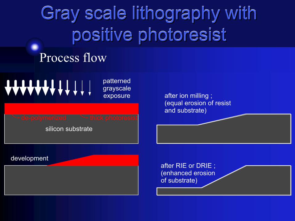
Gray scale lithography with positive photoresist
Gray scale lithography with Gray scale lithography with positive photoresistpositive photoresist
Process flow
silicon substrate
thick photoresist
patternedgrayscaleexposure
de-polymerized
development
after ion milling ;(equal erosion of resistand substrate)
after RIE or DRIE ;(enhanced erosionof substrate)
Gray scale lithography with positive photoresist
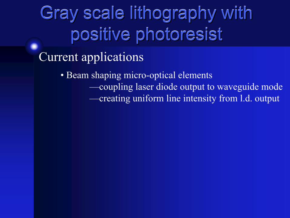
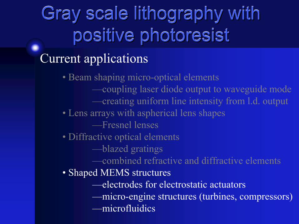
Gray scale lithography with Gray scale lithography with positive photoresistpositive photoresist
Current applications• Beam shaping micro-optical elements
—coupling laser diode output to waveguide mode—creating uniform line intensity from l.d. output
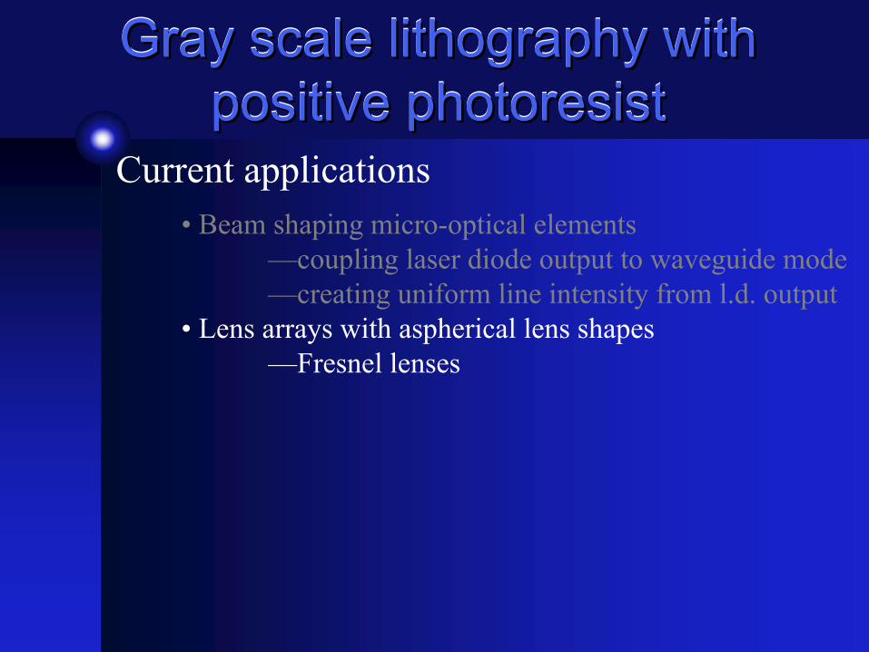
Gray scale lithography with positive photoresist
Gray scale lithography with Gray scale lithography with positive photoresistpositive photoresist
Current applications• Beam shaping micro-optical elements
—coupling laser diode output to waveguide mode—creating uniform line intensity from l.d. output
• Lens arrays with aspherical lens shapes—Fresnel lenses
• Diffractive optical elements—blazed gratings—combined refractive and diffractive elements
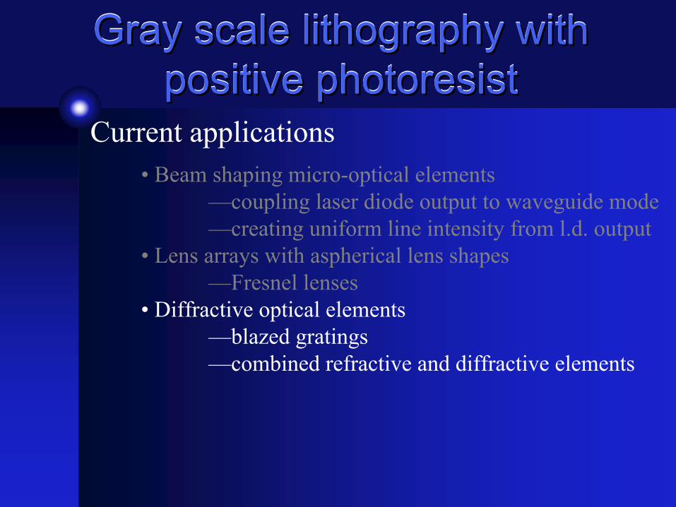
• Shaped MEMS structures—electrodes for electrostatic actuators—micro-engine structures (turbines, compressors)—microfluidics
Gray scale lithography with negative photoresist
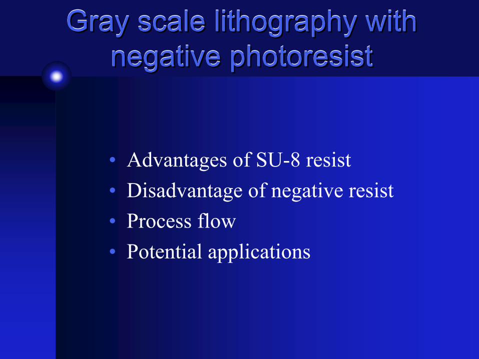
Gray scale lithography with Gray scale lithography with negative photoresistnegative photoresist
• Advantages of SU-8 resist• Disadvantage of negative resist• Process flow• Potential applications
Gray scale lithography with negative photoresist
Gray scale lithography with Gray scale lithography with negative photoresistnegative photoresist
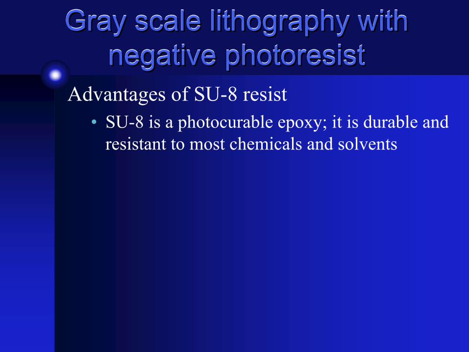
Advantages of SU-8 resist• SU-8 is a photocurable epoxy; it is durable and
resistant to most chemicals and solvents
Gray scale lithography with negative photoresist
Gray scale lithography with Gray scale lithography with negative photoresistnegative photoresist
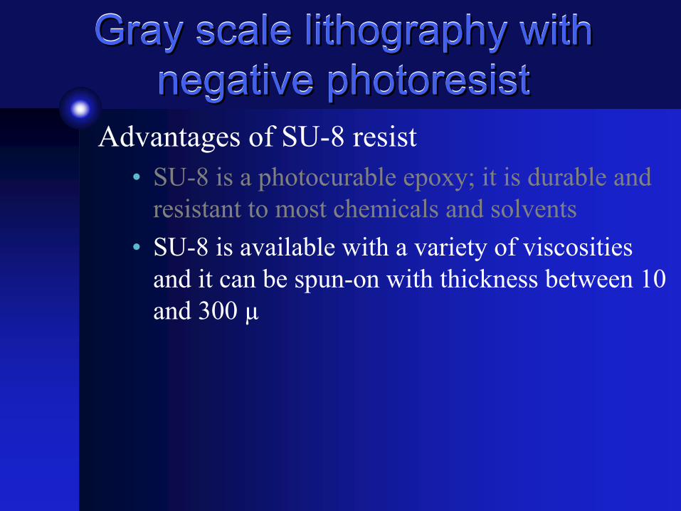
Advantages of SU-8 resist• SU-8 is a photocurable epoxy; it is durable and
resistant to most chemicals and solvents• SU-8 is available with a variety of viscosities
and it can be spun-on with thickness between 10 and 300 µ
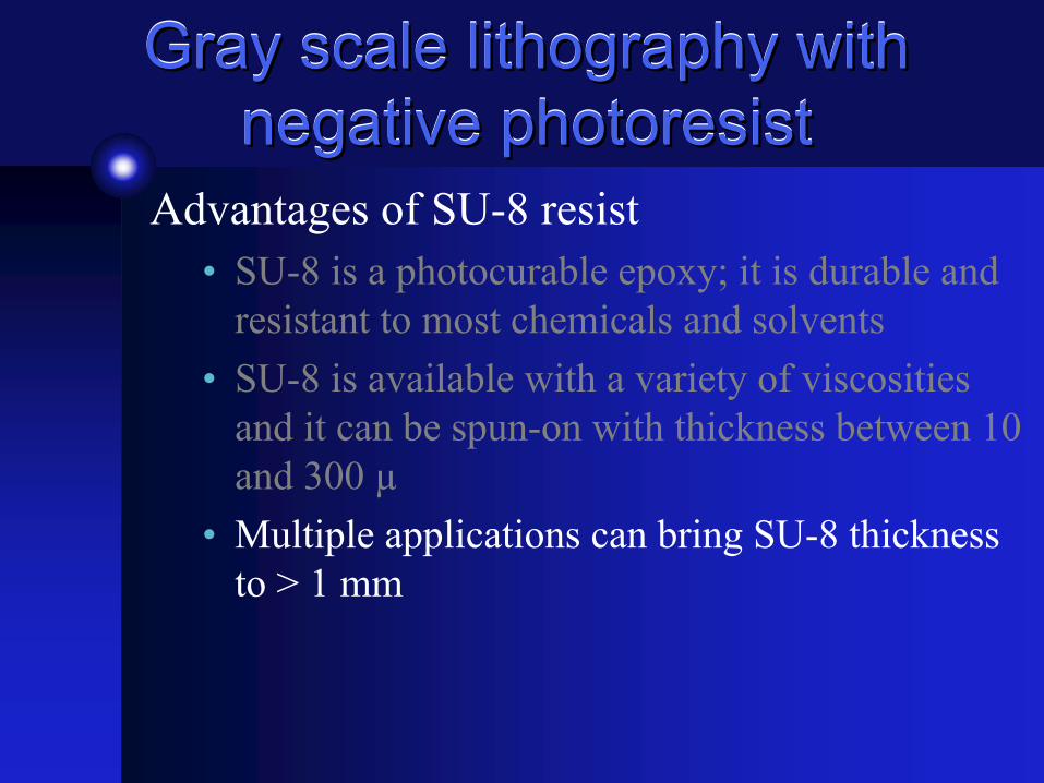
Gray scale lithography with negative photoresist
Gray scale lithography with Gray scale lithography with negative photoresistnegative photoresist
Advantages of SU-8 resist• SU-8 is a photocurable epoxy; it is durable and
resistant to most chemicals and solvents• SU-8 is available with a variety of viscosities
and it can be spun-on with thickness between 10 and 300 µ
• Multiple applications can bring SU-8 thickness to > 1 mm
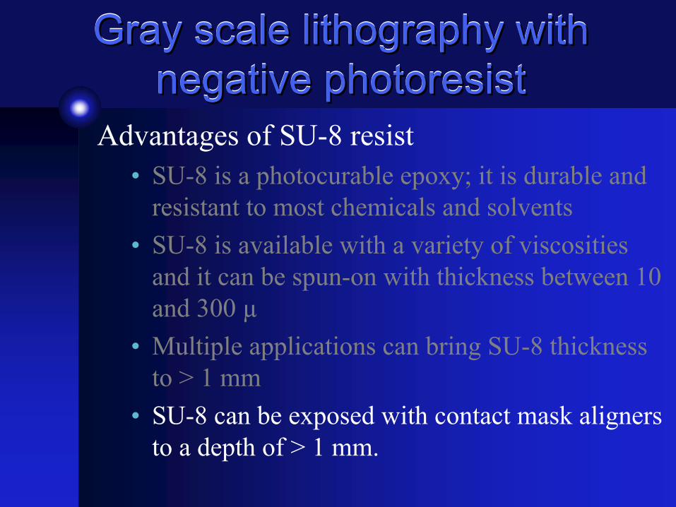
• SU-8 can be exposed with contact mask aligners to a depth of > 1 mm.
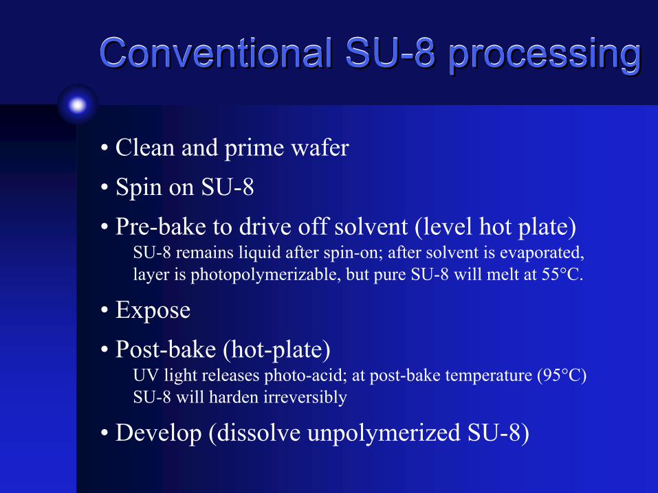
Conventional SU-8 processingConventional SUConventional SU--8 processing8 processing
• Clean and prime wafer• Spin on SU-8• Pre-bake to drive off solvent (level hot plate)
SU-8 remains liquid after spin-on; after solvent is evaporated,layer is photopolymerizable, but pure SU-8 will melt at 55°C.
• Expose• Post-bake (hot-plate)
UV light releases photo-acid; at post-bake temperature (95°C)SU-8 will harden irreversibly
• Develop (dissolve unpolymerized SU-8)
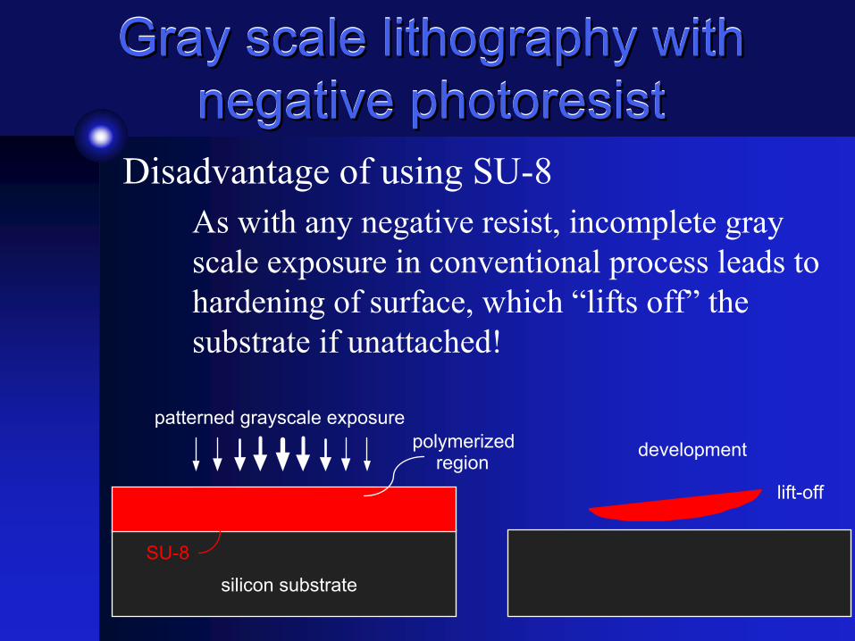
Gray scale lithography with negative photoresist
Gray scale lithography with Gray scale lithography with negative photoresistnegative photoresist
Disadvantage of using SU-8As with any negative resist, incomplete gray scale exposure in conventional process leads to hardening of surface, which “lifts off” the substrate if unattached!
silicon substrate
SU-8
polymerizedregion
patterned grayscale exposure
lift-off
development
Gray scale lithography with negative photoresist
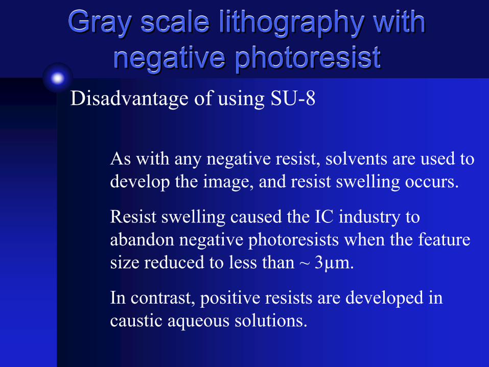
Gray scale lithography with Gray scale lithography with negative photoresistnegative photoresist
Disadvantage of using SU-8
As with any negative resist, solvents are used to develop the image, and resist swelling occurs.
Resist swelling caused the IC industry to abandon negative photoresists when the feature size reduced to less than ~ 3µm.
In contrast, positive resists are developed in caustic aqueous solutions.
Gray scale lithography with negative photoresist
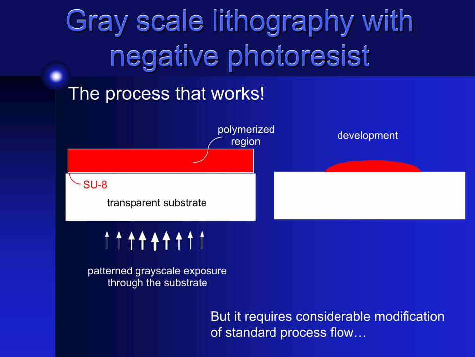
Gray scale lithography with Gray scale lithography with negative photoresistnegative photoresist
The process that works!
transparent substrate
SU-8
patterned grayscale exposurethrough the substrate
development polymerizedregion
But it requires considerable modification of standard process flow…
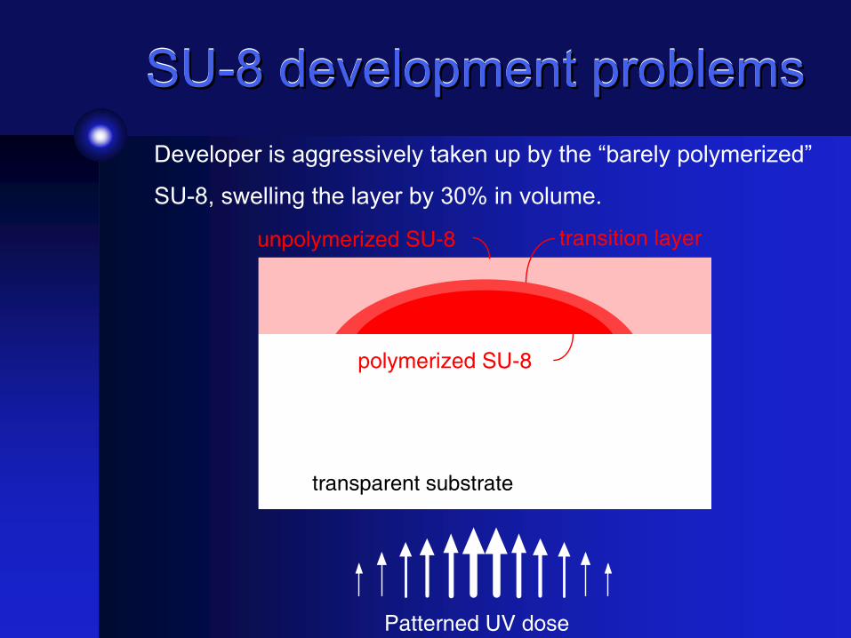
SU-8 development problemsSUSU--8 development problems8 development problemsDeveloper is aggressively taken up by the “barely polymerized”
SU-8, swelling the layer by 30% in volume.
Patterned UV dose
polymerized SU-8
unpolymerized SU-8 transition layer
transparent substrate
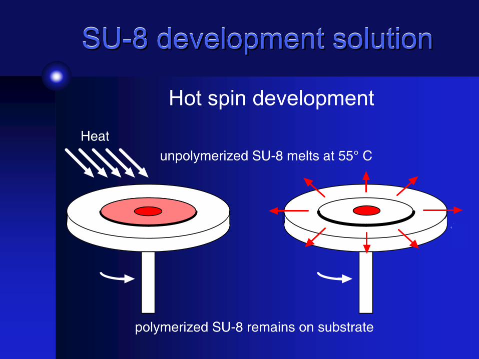
SU-8 development solutionSUSU--8 development solution8 development solution
Hot spin development
Heat
unpolymerized SU-8 melts at 55° C
polymerized SU-8 remains on substrate
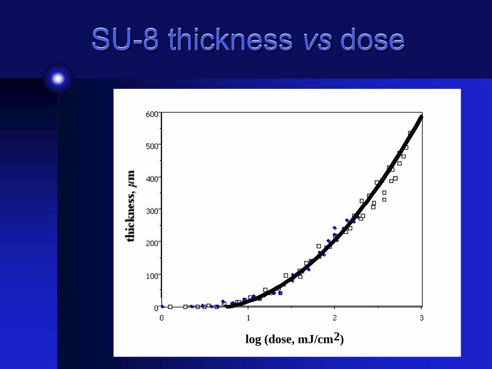
SU-8 thickness vs doseSUSU--8 thickness 8 thickness vsvs dosedose
log (dose, mJ/cm2)
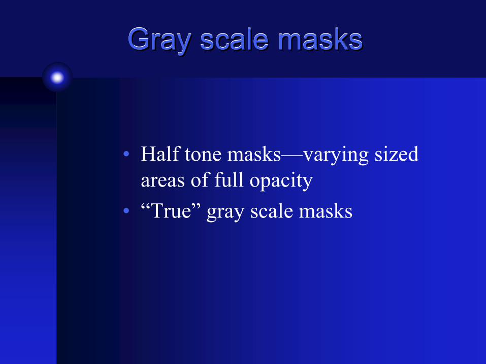
Gray scale masksGray scale masksGray scale masks
• Half tone masks—varying sized areas of full opacity
• “True” gray scale masks
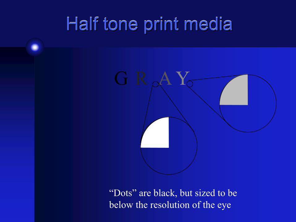
Half tone print mediaHalf tone print mediaHalf tone print media
G R A Y
“Dots” are black, but sized to bebelow the resolution of the eye
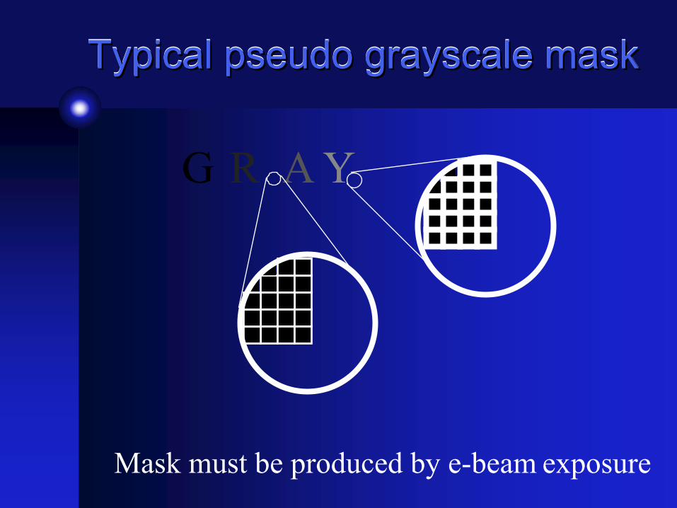
Typical pseudo grayscale maskTypical pseudo grayscale maskTypical pseudo grayscale mask
G R A Y
Mask must be produced by e-beam exposure
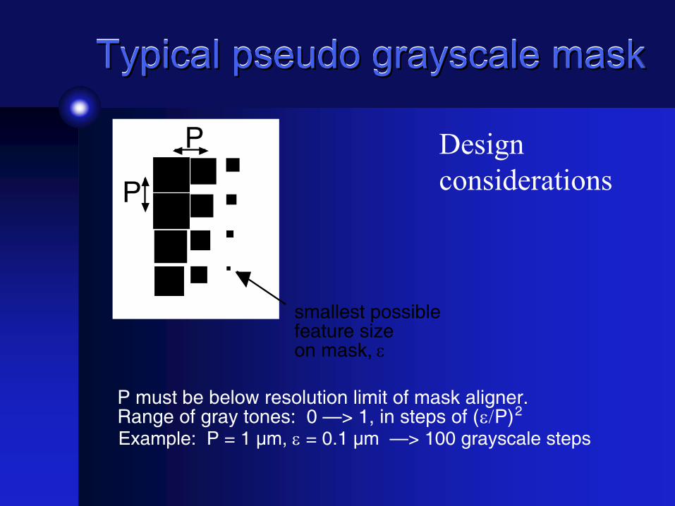
Typical pseudo grayscale maskTypical pseudo grayscale maskTypical pseudo grayscale mask
Design considerations
P
P
smallest possible feature size on mask, ε
P must be below resolution limit of mask aligner. Range of gray tones: 0 —> 1, in steps of (ε/P)2
Example: P = 1 µm, ε = 0.1 µm —> 100 grayscale steps
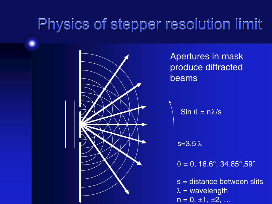
Physics of stepper resolution limitPhysics of stepper resolution limitPhysics of stepper resolution limit
Sin θ = nλ/s
s=3.5 λ
θ = 0, 16.6°, 34.85°,59°
Apertures in maskproduce diffractedbeams
s = distance between slitsλ = wavelengthn = 0, ±1, ±2, …
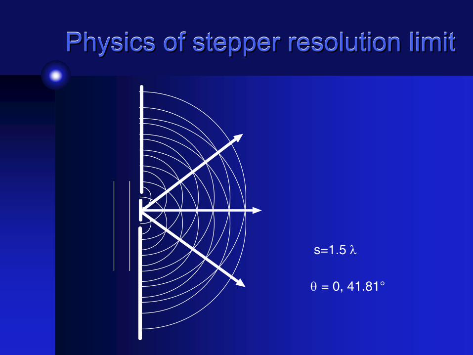
Physics of stepper resolution limitPhysics of stepper resolution limitPhysics of stepper resolution limit
s=1.5 λ
θ = 0, 41.81°
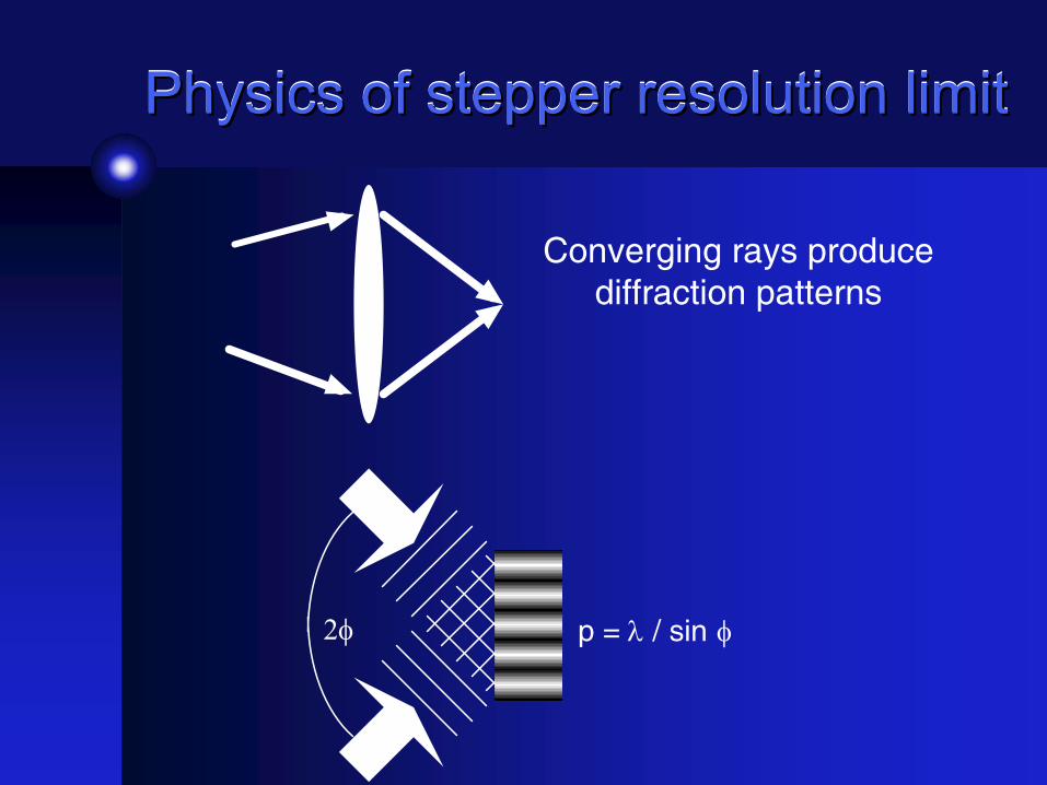
Physics of stepper resolution limitPhysics of stepper resolution limitPhysics of stepper resolution limit
2φ p = λ / sin φ
Converging rays producediffraction patterns
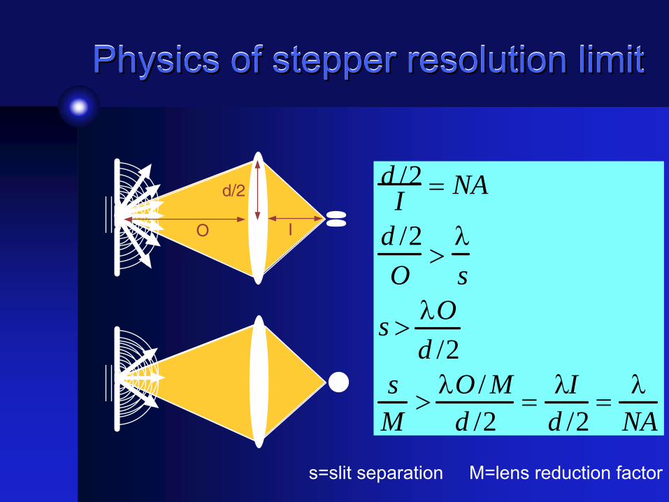
Physics of stepper resolution limitPhysics of stepper resolution limitPhysics of stepper resolution limit
d/2
O I
d /2I
= NA
d /2
O>
λs
s > λO
d /2sM
> λO / Md /2
= λId /2
= λNA
s=slit separation M=lens reduction factor
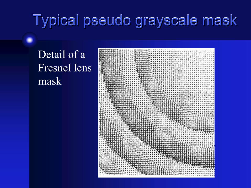
Typical pseudo grayscale maskTypical pseudo grayscale maskTypical pseudo grayscale mask
Detail of a Fresnel lensmask
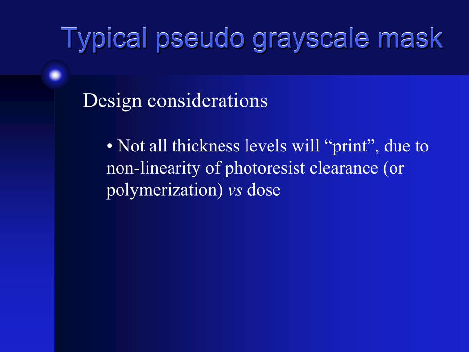
Typical pseudo grayscale maskTypical pseudo grayscale maskTypical pseudo grayscale mask
Design considerations
• Not all thickness levels will “print”, due to non-linearity of photoresist clearance (or polymerization) vs dose
Typical pseudo grayscale maskTypical pseudo grayscale maskTypical pseudo grayscale mask
Design considerations
• Not all thickness levels will “print”, due to non-linearity of photoresist clearance (or polymerization) vs dose
• Mask design depends critically on a stable, consistent, reproducible lithographic process!
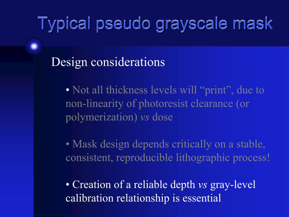
• Creation of a reliable depth vs gray-level calibration relationship is essential
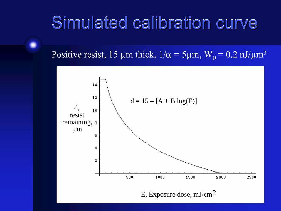
Simulated calibration curveSimulated calibration curveSimulated calibration curve
Positive resist, 15 µm thick, 1/α = 5µm, W0 = 0.2 nJ/µm3
d = 15 – [A + B log(E)]
E, Exposure dose, mJ/cm2
d, resist
remaining, µm
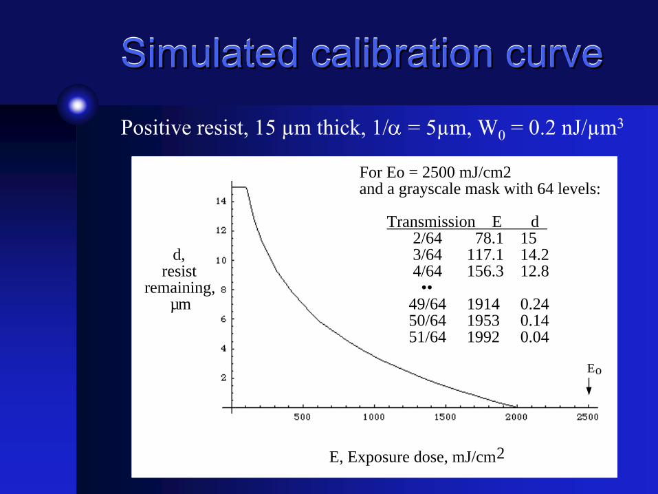
Simulated calibration curveSimulated calibration curveSimulated calibration curve
Positive resist, 15 µm thick, 1/α = 5µm, W0 = 0.2 nJ/µm3
d = 15 – [A + B log(E)]
,
E, Exposure dose, mJ/cm2
d, resist
remaining, µm
Eo
For Eo = 2500 mJ/cm2and a grayscale mask with 64 levels:
Transmission E d 2/64 78.1 15 3/64 117.1 14.2 4/64 156.3 12.8 •• 49/64 1914 0.24 50/64 1953 0.14 51/64 1992 0.04
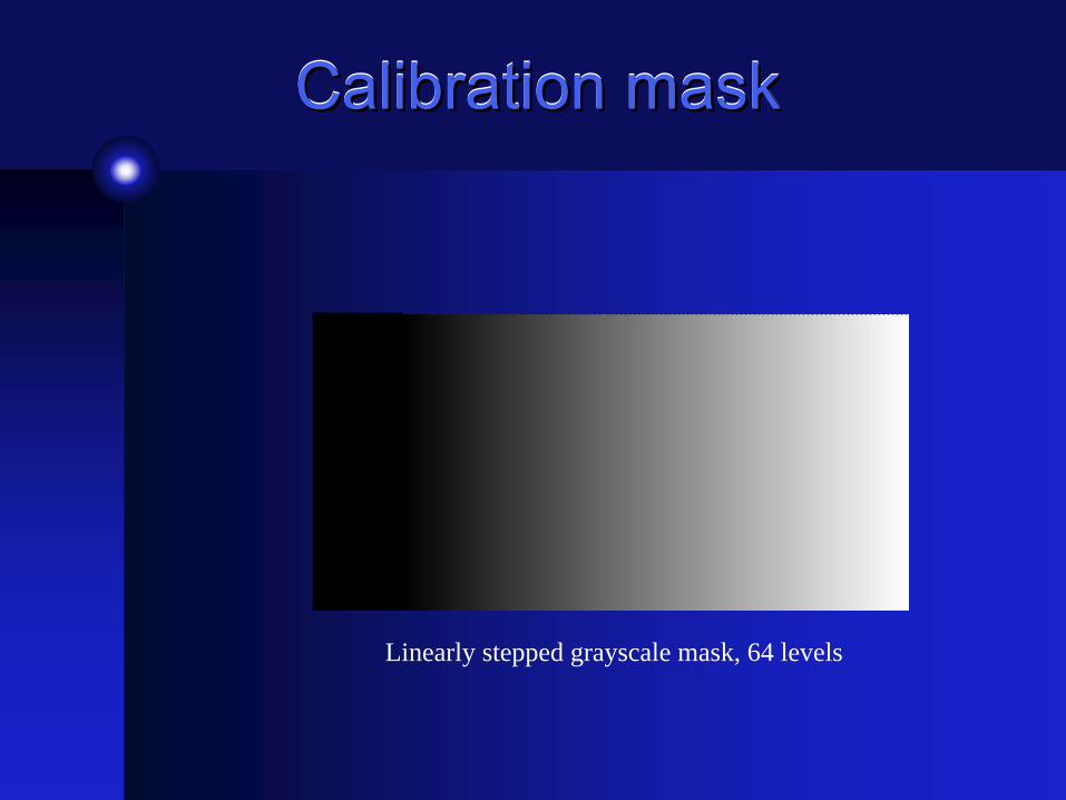
Calibration maskCalibration maskCalibration mask
Linearly stepped grayscale mask, 64 levels
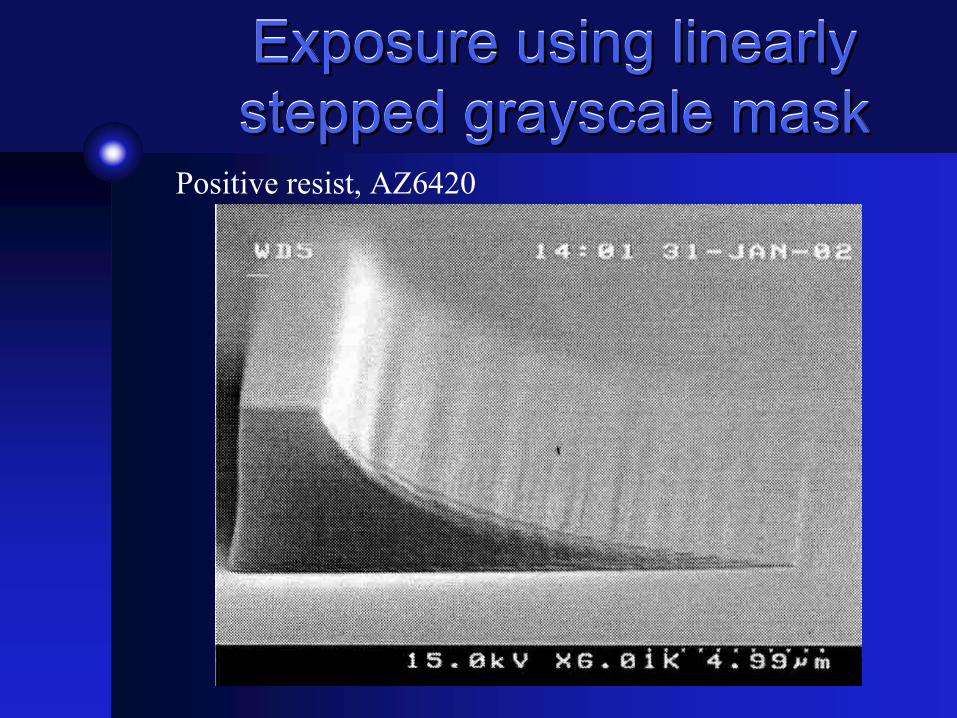
Exposure using linearly stepped grayscale maskExposure using linearly Exposure using linearly stepped grayscale maskstepped grayscale mask
Positive resist, AZ6420
True grayscale masksTrue grayscale masksTrue grayscale masks
• HEBS glass• Thermal bimetallic films• Black & white photographic film
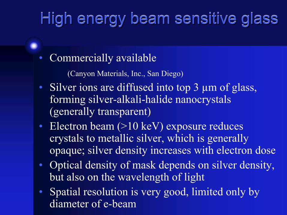
High energy beam sensitive glassHigh energy beam sensitive glassHigh energy beam sensitive glass
• Commercially available (Canyon Materials, Inc., San Diego)
• Silver ions are diffused into top 3 µm of glass, forming silver-alkali-halide nanocrystals(generally transparent)
• Electron beam (>10 keV) exposure reduces crystals to metallic silver, which is generally opaque; silver density increases with electron dose
• Optical density of mask depends on silver density, but also on the wavelength of light
• Spatial resolution is very good, limited only by diameter of e-beam
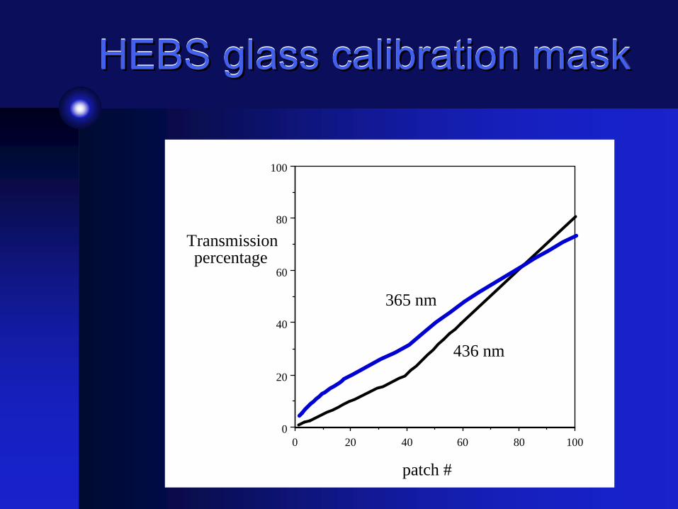
HEBS glass calibration maskHEBS glass calibration maskHEBS glass calibration mask
1008060402000
20
40
60
80
100
patch #
365 nm
436 nm
Transmissionpercentage
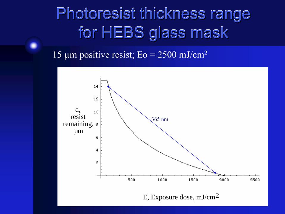
Photoresist thickness rangefor HEBS glass mask
Photoresist thickness rangePhotoresist thickness rangefor HEBS glass maskfor HEBS glass mask
15 µm positive resist; Eo = 2500 mJ/cm2
d = 15 – [A + B log(E)]
E, Exposure dose, mJ/cm2
d, resist
remaining, µm
365 nm
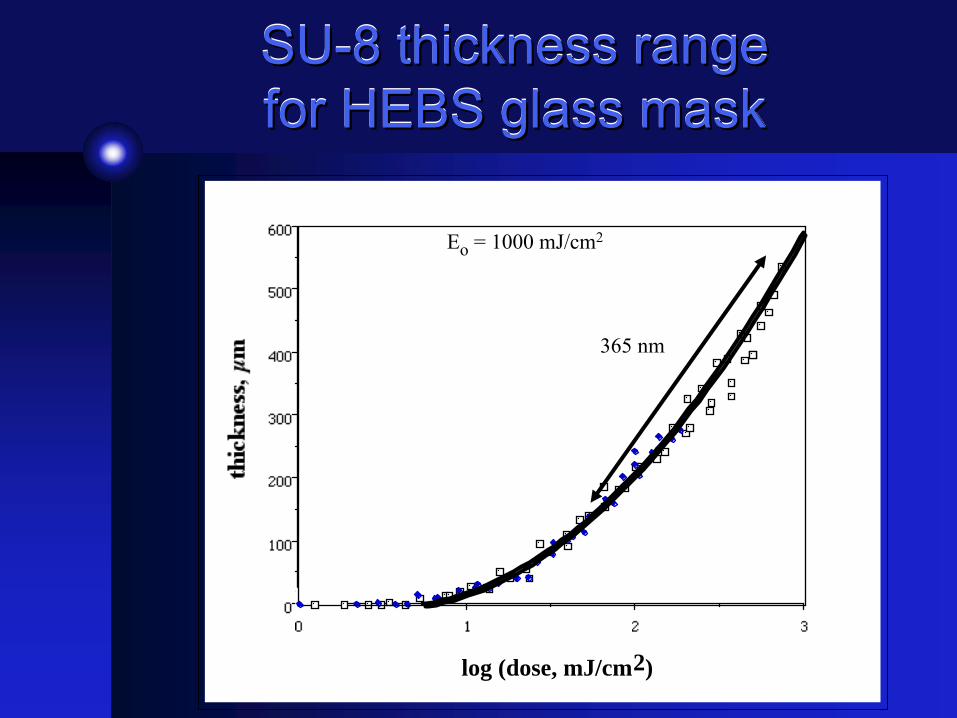
SU-8 thickness rangefor HEBS glass maskSUSU--8 thickness range8 thickness rangefor HEBS glass maskfor HEBS glass mask
log (dose, mJ/cm2)
365 nm
Eo = 1000 mJ/cm2
Proposed grayscale maskProposed grayscale maskProposed grayscale mask
• Bimetallic films on glass (Bi/In or Sn/In)• Film thickness: 10 – 100 nm• Laser exposure (heating) converts opaque
metals to transparent mixed oxides• Completeness of oxide conversion depends
on time @ temperature• OD range: 3.0 to 0.22 at 365 nm• Spatial resolution: ~ 100 nm
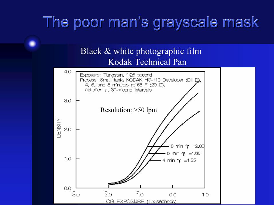
The poor man’s grayscale maskThe poor man’s grayscale maskThe poor man’s grayscale mask
Black & white photographic filmKodak Technical Pan
Resolution: >50 lpm
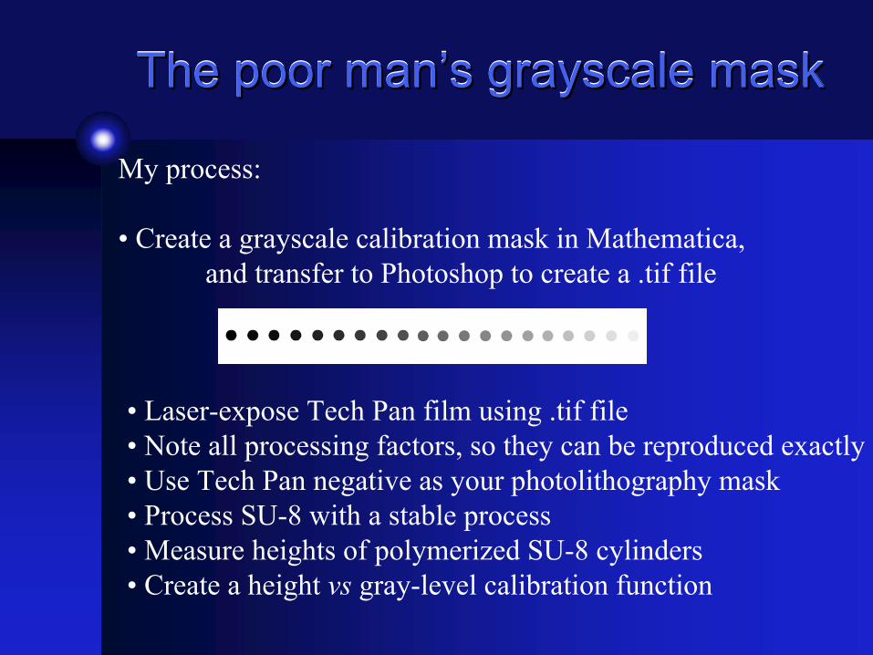
The poor man’s grayscale maskThe poor man’s grayscale maskThe poor man’s grayscale mask
My process:
• Create a grayscale calibration mask in Mathematica, and transfer to Photoshop to create a .tif file
• Laser-expose Tech Pan film using .tif file• Note all processing factors, so they can be reproduced exactly• Use Tech Pan negative as your photolithography mask• Process SU-8 with a stable process• Measure heights of polymerized SU-8 cylinders• Create a height vs gray-level calibration function
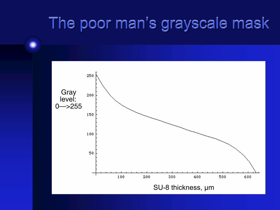
The poor man’s grayscale maskThe poor man’s grayscale maskThe poor man’s grayscale mask
SU-8 thickness, µm
Graylevel:
0—>255
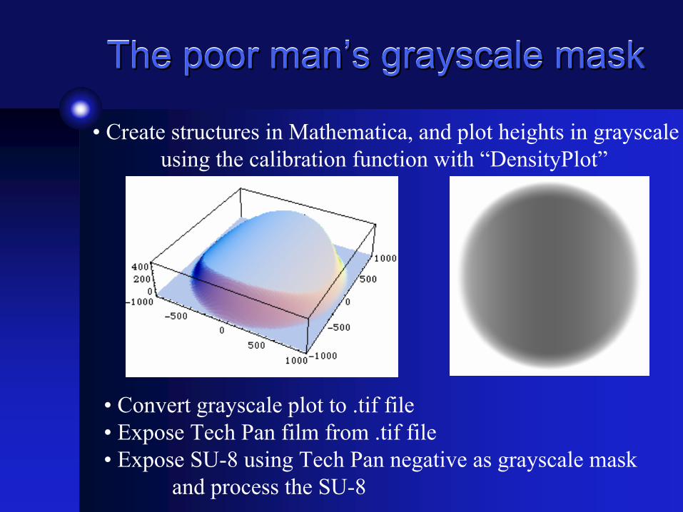
The poor man’s grayscale maskThe poor man’s grayscale maskThe poor man’s grayscale mask
• Create structures in Mathematica, and plot heights in grayscaleusing the calibration function with “DensityPlot”
• Convert grayscale plot to .tif file• Expose Tech Pan film from .tif file• Expose SU-8 using Tech Pan negative as grayscale mask
and process the SU-8
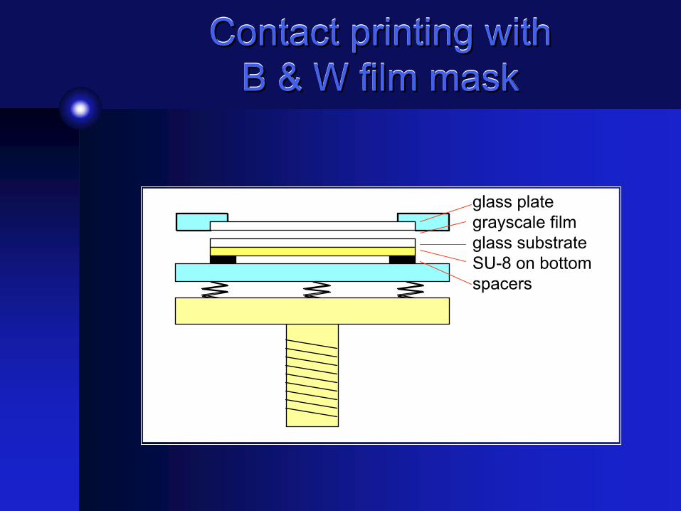
Contact printing with B & W film mask
Contact printing with Contact printing with B & W film maskB & W film mask
glass plategrayscale filmglass substrateSU-8 on bottomspacers
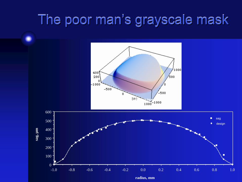
The poor man’s grayscale maskThe poor man’s grayscale maskThe poor man’s grayscale mask
1.00.80.60.40.20.0-0.2-0.4-0.6-0.8-1.00
100
200
300
400
500
600
sag
design
WIT12 Cylinder lens
radius, mm
sag,
µm
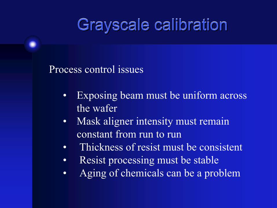
Grayscale calibrationGrayscale calibrationGrayscale calibration
Process control issues
• Exposing beam must be uniform across the wafer
• Mask aligner intensity must remain constant from run to run
• Thickness of resist must be consistent• Resist processing must be stable• Aging of chemicals can be a problem
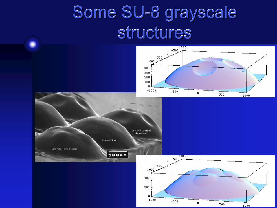
Some SU-8 grayscale structures
Some SUSome SU--8 grayscale 8 grayscale structuresstructures
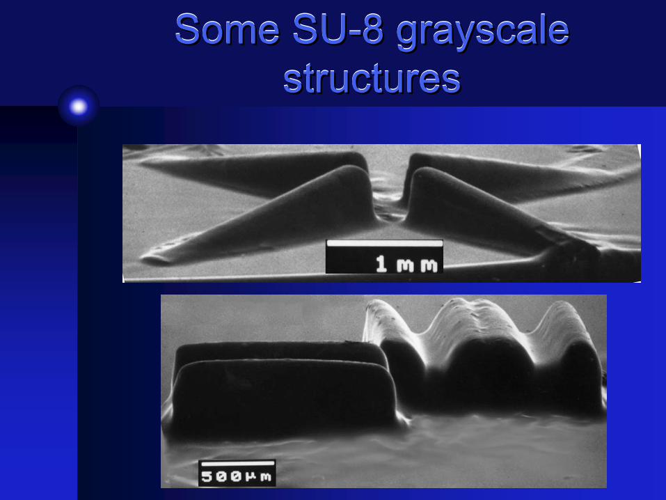
Some SU-8 grayscale structures
Some SUSome SU--8 grayscale 8 grayscale structuresstructures
Micro stereo lithographyMicro stereo lithographyMicro stereo lithography
• Applications• General methods• Details• New directions
Micro stereo lithographyMicro stereo lithographyMicro stereo lithography
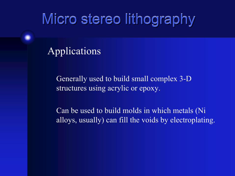
Applications
Generally used to build small complex 3-D structures using acrylic or epoxy.
Can be used to build molds in which metals (Ni alloys, usually) can fill the voids by electroplating.
Micro stereo lithographyMicro stereo lithographyMicro stereo lithography
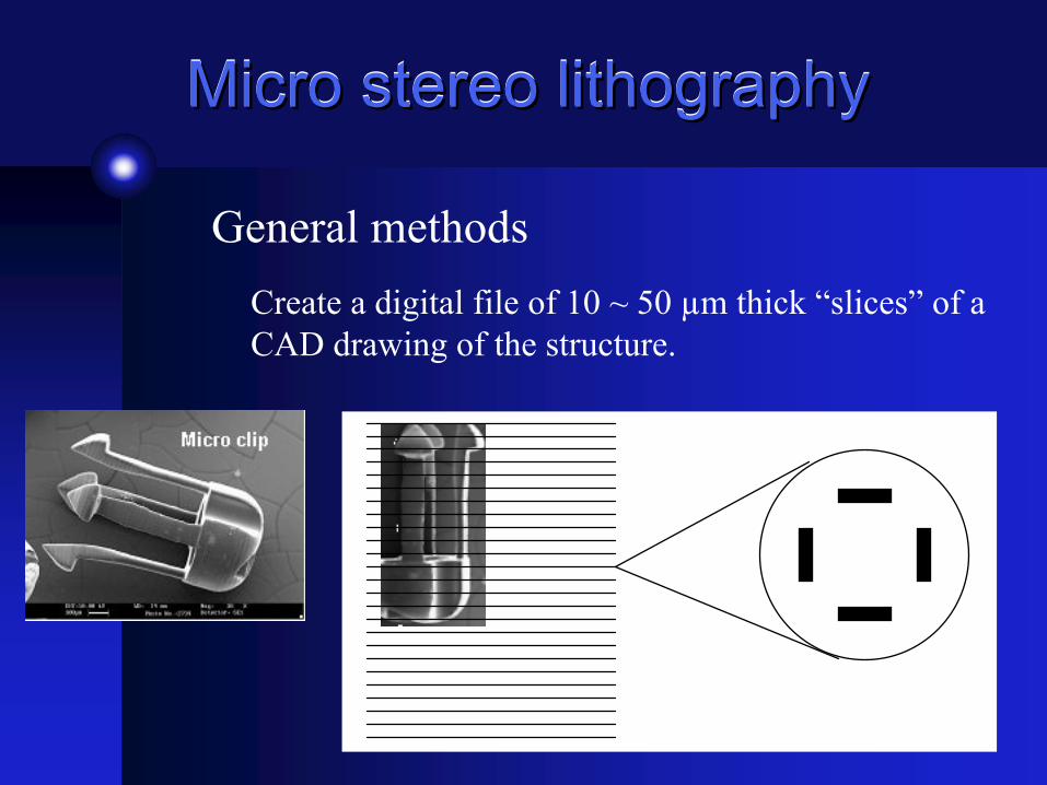
General methodsCreate a digital file of 10 ~ 50 µm thick “slices” of a CAD drawing of the structure.
Micro stereo lithographyMicro stereo lithographyMicro stereo lithography
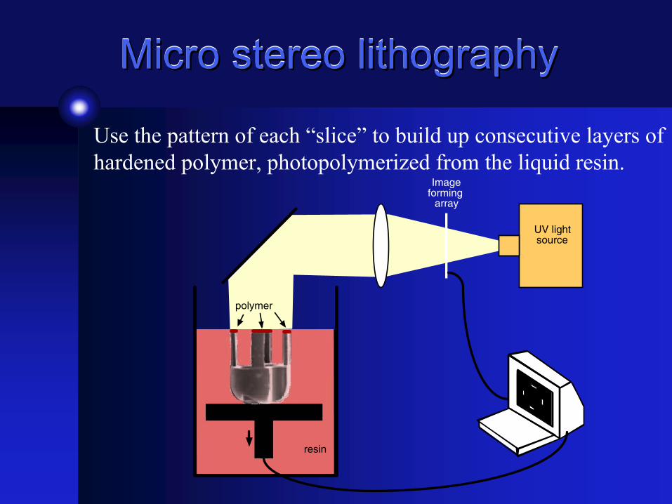
Use the pattern of each “slice” to build up consecutive layers of hardened polymer, photopolymerized from the liquid resin.
UV lightsource
Imageforming
array
resin
polymer
Micro stereo lithographyMicro stereo lithographyMicro stereo lithography
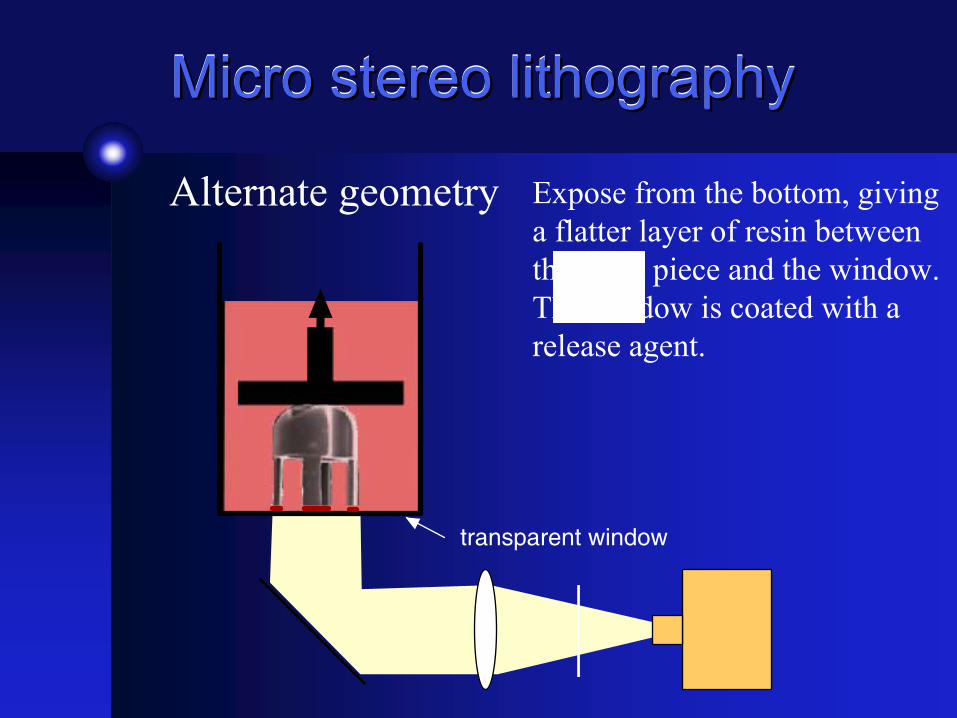
Expose from the bottom, giving a flatter layer of resin between the work piece and the window. The window is coated with a release agent.
transparent window
Alternate geometry
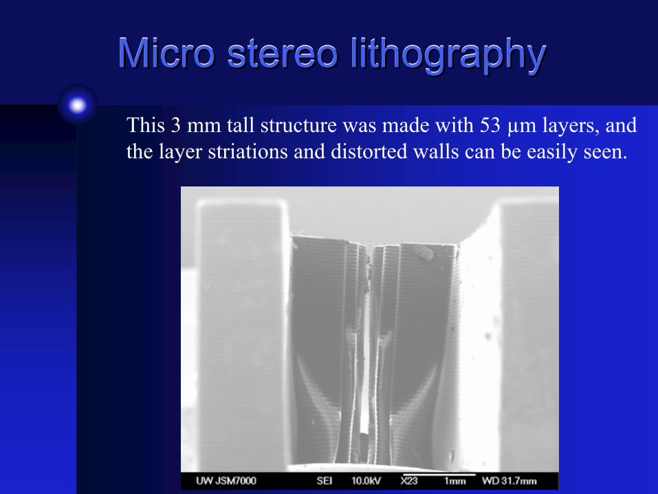
Micro stereo lithographyMicro stereo lithographyMicro stereo lithographyThis 3 mm tall structure was made with 53 µm layers, and the layer striations and distorted walls can be easily seen.
Micro stereo lithographyMicro stereo lithographyMicro stereo lithography
New directions
Directly create ceramic structures by loading resin with ceramic particles, and firing structure to vaporize the polymer and fuse the ceramic. With proper loading and firing, little volume change occurs.
Directly create metallic structures by loading resin with metal particles, etc.
Two-photon lithographyTwoTwo--photon lithographyphoton lithography
• Overview• Details• Potential new directions
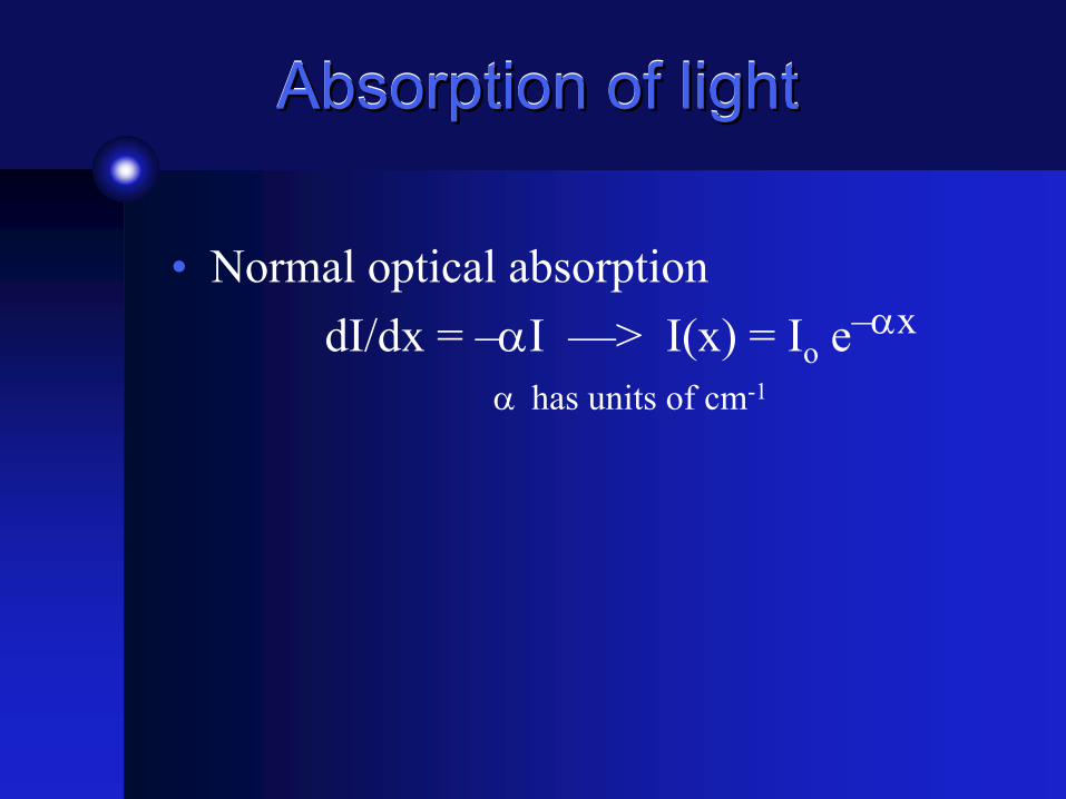
Absorption of lightAbsorption of lightAbsorption of light
• Normal optical absorptiondI/dx = –αI —> I(x) = Io e–αx
α has units of cm-1
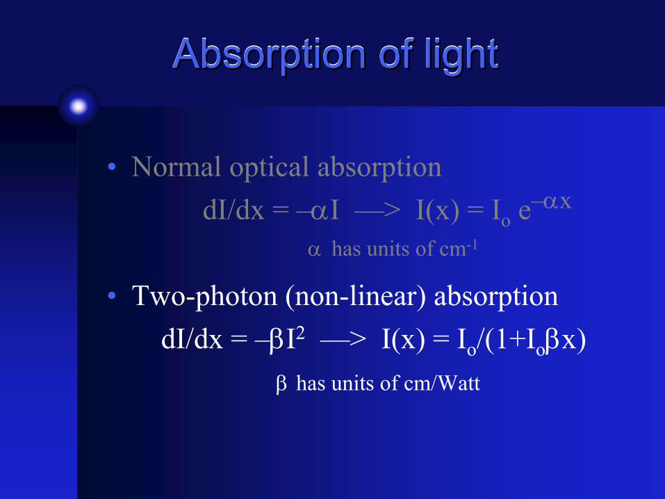
Absorption of lightAbsorption of lightAbsorption of light
• Normal optical absorptiondI/dx = –αI —> I(x) = Io e–αx
α has units of cm-1
• Two-photon (non-linear) absorptiondI/dx = –βI2 —> I(x) = Io/(1+Ioβx)
β has units of cm/Watt
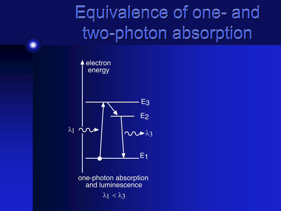
Equivalence of one- and two-photon absorption
Equivalence of oneEquivalence of one-- and and twotwo--photon absorptionphoton absorptionelectron energy
E3
E1
E2
one-photon absorptionand luminescence
λ1 λ3
λ1 < λ3
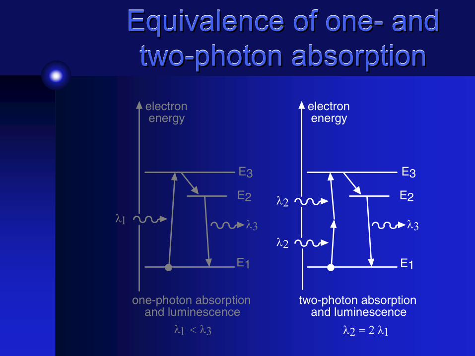
Equivalence of one- and two-photon absorption
Equivalence of oneEquivalence of one-- and and twotwo--photon absorptionphoton absorptionelectron energy
E3
E1
E2
one-photon absorptionand luminescence
λ1 λ3
λ1 < λ3
electron energy
E3
E1
E2
two-photon absorptionand luminescence
λ3
λ2
λ2
λ2 = 2 λ1
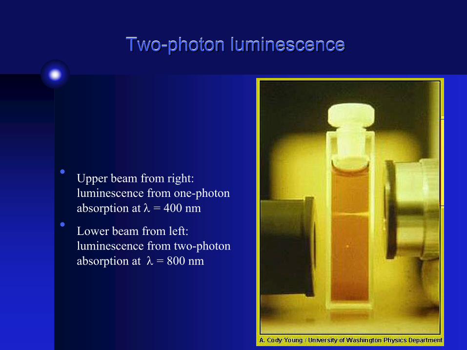
Two-photon luminescenceTwoTwo--photon luminescencephoton luminescence
• Upper beam from right: luminescence from one-photon absorption at λ = 400 nm
• Lower beam from left: luminescence from two-photon absorption at λ = 800 nm
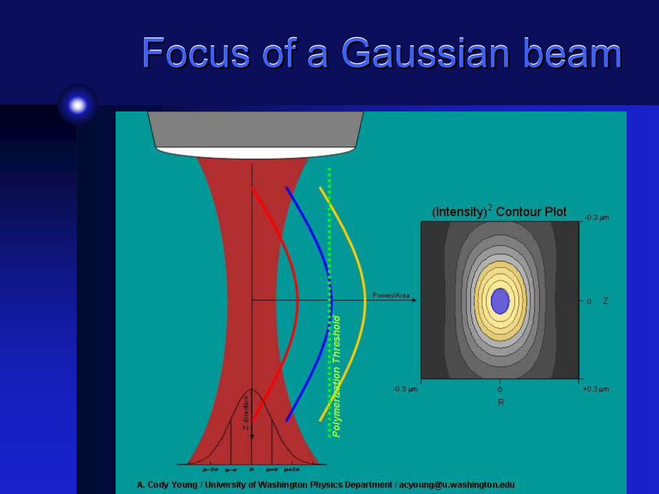
Focus of a Gaussian beamFocus of a Gaussian beamFocus of a Gaussian beam
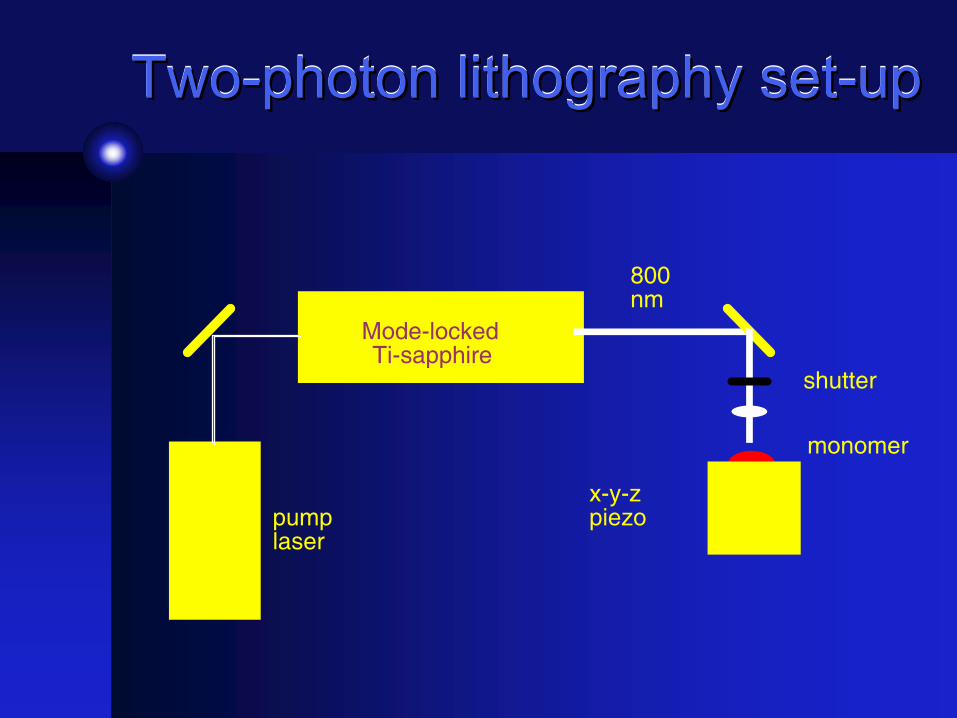
Two-photon lithography set-upTwoTwo--photon lithography setphoton lithography set--upup
pump laser
Mode-lockedTi-sapphire
x-y-z piezo
800nm
monomer
shutter
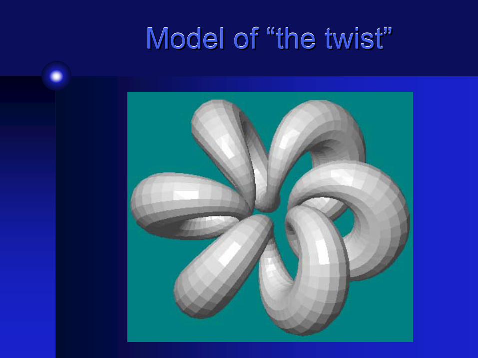
Model of “the twist”Model of “the twist”Model of “the twist”
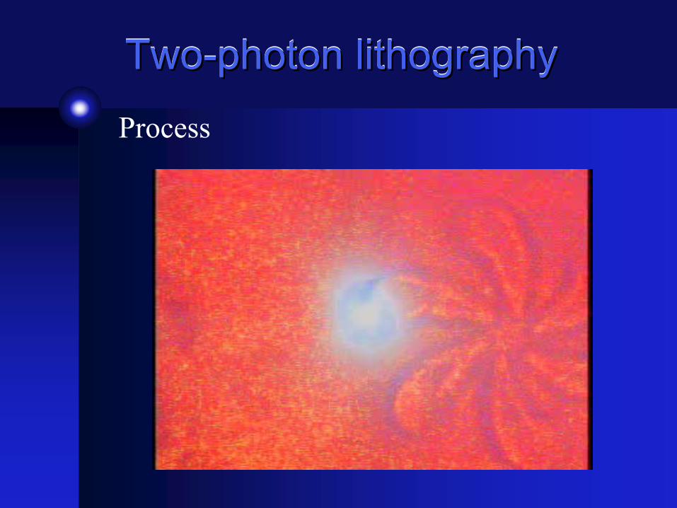
Two-photon lithographyTwoTwo--photon lithographyphoton lithographyProcess
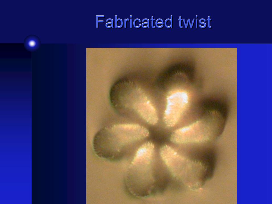
Fabricated twistFabricated twistFabricated twist
The challenge of two-photon lithography
The challenge of The challenge of twotwo--photon lithography photon lithography
• Is there a compelling application?
• Can devices by made cost-effectively?
• Will other techniques catch up?
Current and future researchon two-photon lithography
Current and future researchCurrent and future researchon twoon two--photon lithographyphoton lithography
• Polymerize conducting materials
Current and future researchon two-photon lithography
Current and future researchCurrent and future researchon twoon two--photon lithographyphoton lithography
• Polymerize conducting materials• Polymerize semiconducting materials
Current and future researchon two-photon lithography
Current and future researchCurrent and future researchon twoon two--photon lithographyphoton lithography
• Polymerize conducting materials• Polymerize semiconducting materials• Construct contiguous regions of conductors,
semiconductors and insulators (with 50 nm features)!
• Integrate organic light emitters and other photonic devices in 3-D photonic circuits
Different materials may be polymerizablesimultaneously using different wavelengths, by attaching the different monomers to chromophores with different absorption bands.
Challenges for the future oftwo-photon lithography
Challenges for the future ofChallenges for the future oftwotwo--photon lithographyphoton lithography
• The technique is inherently a unit by unit fabrication method.
Challenges for the future oftwo-photon lithography
Challenges for the future ofChallenges for the future oftwotwo--photon lithographyphoton lithography
• The technique is inherently a unit by unit fabrication method.
• Silicon processing (a mass-production technique) is intent on reaching the 40 nm feature size within 10 years.
• Never underestimate the inventiveness of silicon processing engineers!