Photoelectrochemical studies of DNA-tagged biomolecules … studies of DNA-tagged ... biomolecules...
8
NANO EXPRESS Open Access Photoelectrochemical studies of DNA-tagged biomolecules on Au and Au/Ni/Au multilayer nanowires Viswanathan Swaminathan, Hwi Fen Liew, Wen Siang Lew * , Lanying Hu and Anh Tuan Phan Abstract The use of nanowires (NWs) for labeling, sensing, and sorting is the basis of detecting biomolecules attached on NWs by optical and magnetic properties. In spite of many advantages, the use of biomolecules-attached NWs sensing by photoelectrochemical (PEC) study is almost non-existent. In this article, the PEC study of dye-attached single-stranded DNA on Au NWs and Au-Ni-Au multilayer NWs prepared by pulse electrodeposition are investigated. Owing to quantum-quenching effect, the multilayer Au NWs exhibit low optical absorbance when compared with Au NWs. The tagged Au NWs show good fluorescence (emission) at 570 nm, indicating significant improvement in the reflectivity. Optimum results obtained for tagged Au NWs attached on functionalized carbon electrodes and its PEC behavior is also presented. A twofold enhancement in photocurrent is observed with an average dark current of 10 μA for Au NWs coated on functionalized sensing electrode. The importance of these PEC and optical studies provides an inexpensive and facile processing platform for Au NWs that may be suitable for biolabeling applications. Introduction Gold (Au) nanostructures have paved the way to map out a novel platform for designing nano biobarcode for a wide range of biosensing applications [1]. Au nanoma- terials, such as nanoparticles, nanowires (NWs), and nanorods, are the widely studied materials which have great demand in the scientific community [2,3]. Interest- ingly, they offer a number of properties that make them suitable for use in biological applications, such as bio- sensing [4], biosorting [5], and biolabelling [6]. The structure and composition in multilayered gold NWs will escalate the development of bio-nanotechnology when compared with nanoparticles [7]. In particular, 1D Au nanostructures have a strong optical property that can be tuned by controlling the wire length and dia- meter of the NWs and multilayer NWs [8]. Moreover, the optical absorption coefficient of gold NWs is much higher than those of gold nanoparticles [9-11]. The fab- ricated NWs are tagged with various DNA libraries, antibodies, or antigens that can be used for sensing or labeling at a time of different biological assays through direct chemical reactions [12]. A suitable synthesis technique is needed to control the shape and size of the NWs to improve the biocompat- ibility for biosensing applications. The most direct approach of controlled synthesis of NWs is produced by electrochemical routes [13]. High aspect ratio NWs have more intense reflection and scattering properties; domi- nated by the polarization-dependent plasmon resonance between the metallic layers rather than by the bulk metallic reflectance [12]. The identification of tagged biomolecules on the surface of nanomaterials can be encoded and easily read out through optical microscope [14]. The optical properties of Au or Au stripes nanos- tructures [15], optical quenching [16], and the NW aggregation [17] have widely been reported, but the understanding of surface plasmon for multilayer NWs is still to be explored. Hence, it is important to study the shape of multilayer NWs that affects the surface plas- mon [18,19], which is the key area to tune the optical properties of biobarcode in multiplex biolabeling applications. Photoelectrochemical (PEC) measurements have been well exploited for photovoltaic applications, but the * Correspondence: [email protected] School of Physical and Mathematical Sciences, Nanyang Technological University, 21 Nanyang Link, 637371, Singapore Swaminathan et al. Nanoscale Research Letters 2011, 6:535 http://www.nanoscalereslett.com/content/6/1/535 © 2011 Swaminathan et al; licensee Springer. This is an Open Access article distributed under the terms of the Creative Commons Attribution License (http://creativecommons.org/licenses/by/2.0), which permits unrestricted use, distribution, and reproduction in any medium, provided the original work is properly cited.
Transcript of Photoelectrochemical studies of DNA-tagged biomolecules … studies of DNA-tagged ... biomolecules...
NANO EXPRESS Open Access
Photoelectrochemical studies of DNA-taggedbiomolecules on Au and Au/Ni/Au multilayernanowiresViswanathan Swaminathan, Hwi Fen Liew, Wen Siang Lew*, Lanying Hu and Anh Tuan Phan
Abstract
The use of nanowires (NWs) for labeling, sensing, and sorting is the basis of detecting biomolecules attached onNWs by optical and magnetic properties. In spite of many advantages, the use of biomolecules-attached NWssensing by photoelectrochemical (PEC) study is almost non-existent. In this article, the PEC study of dye-attachedsingle-stranded DNA on Au NWs and Au-Ni-Au multilayer NWs prepared by pulse electrodeposition areinvestigated. Owing to quantum-quenching effect, the multilayer Au NWs exhibit low optical absorbance whencompared with Au NWs. The tagged Au NWs show good fluorescence (emission) at 570 nm, indicating significantimprovement in the reflectivity. Optimum results obtained for tagged Au NWs attached on functionalized carbonelectrodes and its PEC behavior is also presented. A twofold enhancement in photocurrent is observed with anaverage dark current of 10 μA for Au NWs coated on functionalized sensing electrode. The importance of thesePEC and optical studies provides an inexpensive and facile processing platform for Au NWs that may be suitablefor biolabeling applications.
IntroductionGold (Au) nanostructures have paved the way to mapout a novel platform for designing nano biobarcode fora wide range of biosensing applications [1]. Au nanoma-terials, such as nanoparticles, nanowires (NWs), andnanorods, are the widely studied materials which havegreat demand in the scientific community [2,3]. Interest-ingly, they offer a number of properties that make themsuitable for use in biological applications, such as bio-sensing [4], biosorting [5], and biolabelling [6]. Thestructure and composition in multilayered gold NWswill escalate the development of bio-nanotechnologywhen compared with nanoparticles [7]. In particular, 1DAu nanostructures have a strong optical property thatcan be tuned by controlling the wire length and dia-meter of the NWs and multilayer NWs [8]. Moreover,the optical absorption coefficient of gold NWs is muchhigher than those of gold nanoparticles [9-11]. The fab-ricated NWs are tagged with various DNA libraries,antibodies, or antigens that can be used for sensing or
labeling at a time of different biological assays throughdirect chemical reactions [12].A suitable synthesis technique is needed to control the
shape and size of the NWs to improve the biocompat-ibility for biosensing applications. The most directapproach of controlled synthesis of NWs is produced byelectrochemical routes [13]. High aspect ratio NWs havemore intense reflection and scattering properties; domi-nated by the polarization-dependent plasmon resonancebetween the metallic layers rather than by the bulkmetallic reflectance [12]. The identification of taggedbiomolecules on the surface of nanomaterials can beencoded and easily read out through optical microscope[14]. The optical properties of Au or Au stripes nanos-tructures [15], optical quenching [16], and the NWaggregation [17] have widely been reported, but theunderstanding of surface plasmon for multilayer NWs isstill to be explored. Hence, it is important to study theshape of multilayer NWs that affects the surface plas-mon [18,19], which is the key area to tune the opticalproperties of biobarcode in multiplex biolabelingapplications.Photoelectrochemical (PEC) measurements have been
well exploited for photovoltaic applications, but the
* Correspondence: [email protected] of Physical and Mathematical Sciences, Nanyang TechnologicalUniversity, 21 Nanyang Link, 637371, Singapore
Swaminathan et al. Nanoscale Research Letters 2011, 6:535http://www.nanoscalereslett.com/content/6/1/535
© 2011 Swaminathan et al; licensee Springer. This is an Open Access article distributed under the terms of the Creative CommonsAttribution License (http://creativecommons.org/licenses/by/2.0), which permits unrestricted use, distribution, and reproduction inany medium, provided the original work is properly cited.
literature is scarce on the detection of biomoleculesusing this approach. PEC is simple and offers an alterna-tive method of detecting biomolecules through molecu-lar binding on a working electrode by electrochemicalroute. Thus, we study the PCE properties of tagged Aunanostructures. In this article, we describe the effect ofsurface plasmon and the variation of luminescenceproperties on shape-controlled Au nanostructures thattagged with thiolated cy3-dye attached on DNA. Wealso study the PEC properties of dye with DNA-taggedAu and multilayer NWs coated on functionalized carbonelectrode.
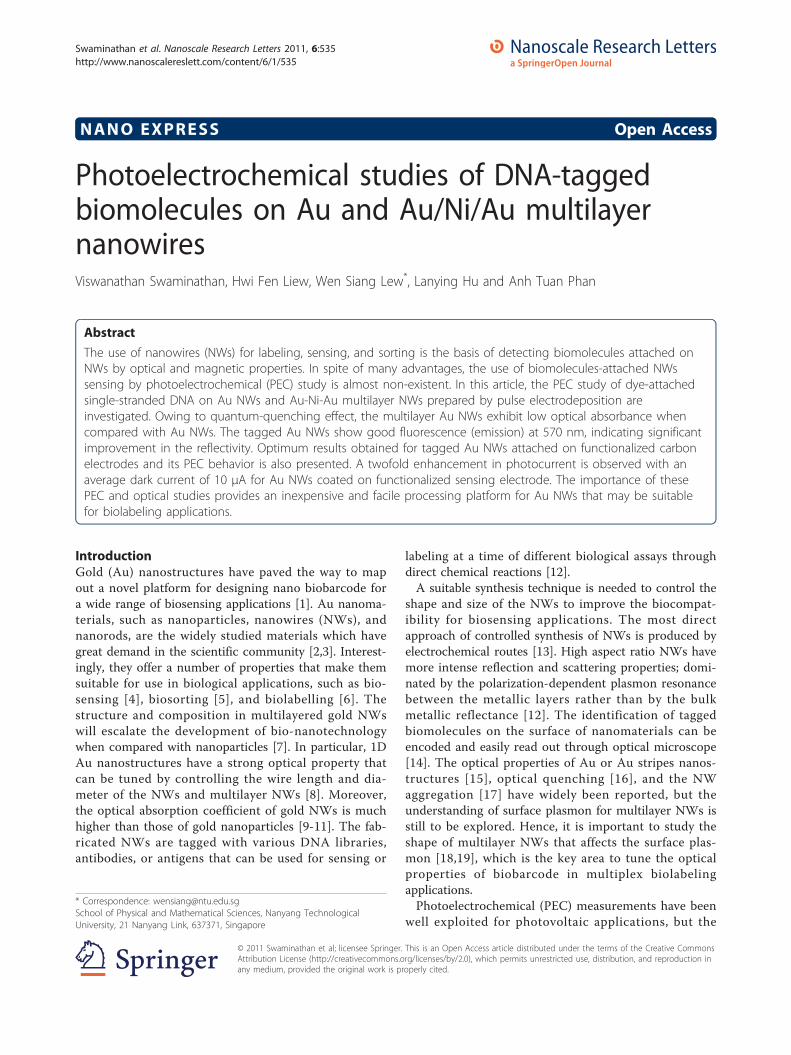
Experimental proceduresFigure 1 depicts the preparation of Au NWs and multi-layer (Au/Ni/Au) NWs. The starting reactants were ofhigh-purity ammonium gold sulfite electroplating solu-tion (Metalor, 99.99%), nickel sulfate hexahyrate, andboric acid (Fisher Scientific) and sodium citrate (SigmaAldrich) for the preparation of Au NWs and multilayerNWs. Deoxyribonucleotide triphosphate (dNTP), fluoro-phores Cy3-dye, and pH 7.4 phosphate buffer solution(PBS) XL (Invitrogen) were used for tagging process. 1-Butyl-3-methylimidazolium hexafluorophosphate
(BMIM-PF6) (Sigma Aldrich) ionic liquid served as cata-lysis for PEC measurements. Anodic aluminum oxide(AAO) template (Anodisc 13, Whatman) of high purityand uniform pore density, with an average pore dia-meter of 200 nm and a template thickness of 60 μm,was employed for pulse electrodeposition [6]. A 200-nmthick copper layer was thermally evaporated onto oneside of the AAO template which acted as the workingelectrode for the pulse electrochemical deposition. Thepulse electrodeposition was carried out on the AAOnanopores, using a standard three-electrode potentiostatsystem (PAR-Verstat-3). A saturated calomel electrode(SCE) was used as the reference electrode, the Cu-coated AAO as cathode, and a platinum mesh was usedas the counter electrode. The preparation of gold andnickel layers was produced from 0.1 M of the ammo-nium gold sulfite electroplating solution and the 0.5 Mof nickel salts; and the brightness of the Ni layer wasenhanced by adding 0.1 M of boric acid. MultilayerNWs were prepared using separate deposition electro-lytes. Under the potentiostatic condition, the depositionpotential of the gold and Ni layers was plated at -1.0 Vversus SCE, and -1.5 V versus SCE, respectively. Threemetallic layers of Au/Ni/Au multilayer NW deposition
Figure 1 Schematic illustration of the synthesis of Au NWs and Au/Ni/Au multilayer NWs using pulse electrochemical depositiontechniques.
Swaminathan et al. Nanoscale Research Letters 2011, 6:535http://www.nanoscalereslett.com/content/6/1/535
Page 2 of 8
were carried out at a three-step process. Deposition timeand pulse period are two key parameters that can beused to control the NWs lengths. Au NWs and multi-layer NWs were separated by etching out the AAOusing 3 M sodium hydroxide (NaOH) solution anddecanting the dissolved alumina. The released NWswere dispersed in isopropanol alcohol (IPA) and a dropof NWs-IPA mixture was coated on Si substrate forfurther analysis.Field emission scanning electron microscope (JSM-
6335 FESEM) was employed to study the morphology ofAu NWs and multilayer NWs. A bright-field reflectanceimages were acquired using an inverted microscope(Olympus BX 51,175 W ozone-free He lamp), equippedwith a color digital video camera (Sony Exwave HAD-12megapixel). All reflectance images were taken at 540nm, which is the wavelength that gives the optimumreflectance area of the Au NWs. A confocal Raman sys-tem (WITEC CRM-200) with a processing time of 0.5 swas used to measure the photoluminescence (PL) spec-trum of Au NWs and multilayer NWs.Au NWs and multilayer NWs (150 μL) were first
incubated with dNTP (0.2 μL, 10 mM) for 15 min.Then, 300 μL buffer containing NaCl (50 mM) andsodium phosphate (5 mM) was added into the mixture.The volume was reduced to 150 μL by vacuum centrifu-gation over 4-5 h at 45°C to gradually increase salt con-centration which is critical to maintain a stable colloidsolution. Then, thiol-DNA was introduced in, followedby heating at 55°C for 3 h. Subsequently, the particleswere washed through centrifugation to remove unboundoligonucleotides. Fluorescence of the tagged DNA ongold was accomplished by means of a fluorophores-Cy3-dye (green emission) which was covalently attached tothe oligonucleotides used in the sequence of (5’-3’):(5ThioMC6-D/TTT TTT TTT TCC CTA ACC CTAACC CTA ACC CTT/3Cy3Sp).PEC measurements were carried out using a three-
electrode electrochemical cell and a light source of200lumens LED (Fenix PP). The resistance of the screenprinted electrode was 50 ± 10 Ω. To improve the con-ductivity of the electrode, 2 μL of BMIM-PF6 ionicliquid was coated on the screen-printed carbon surface.The significance of the ionic liquid is that it canimprove the conductivity, resulting in low ohmic lossesand high rate of mass transfer. Au NWs were thendrop-cast on the functionalized screen-printed electro-des. Before electrochemical detection of biomolecules,the dried electrodes were rinsed with pH of 7.4 PBS forfurther analysis. A three-electrode setup consisting ofthe functionalized electrode as photo cathode, SCE asreference, and the platinum electrode as anode wereused to measure photocurrent upon light irradiation. 20mL of PBS was used as electrolyte; photocurrent was
then recorded as a function of light irradiation. PECmeasurements were taken for raw electrode, dark, andlight current measurements for the surface-modifiedphoto cathode.
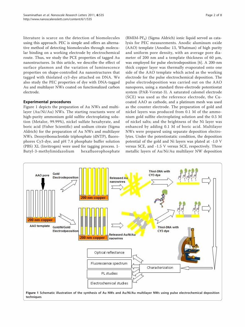
Results and discussionFigure 2a shows a typical FESEM image of pulse electro-deposited Au NWs and multilayer NWs. The diametersof the Au NWs are in the range of approximately 300 ±30 nm. The observed wire length was inhomogeneouspossibly because of the difference in the thickness of thebase substrate layer at each pore, or hydrogen uptake
Figure 2 SEM micrographs of as-prepared (a) Au NWs and (b)Au/Ni/Au multilayer NWs.
Swaminathan et al. Nanoscale Research Letters 2011, 6:535http://www.nanoscalereslett.com/content/6/1/535
Page 3 of 8
which could influence the base crystal nucleation. TheAu NWs are continuous and have an average length of6 μm. The multilayer Au/Ni/Au NWs show a distinctcontrast between gold and Ni layers (Figure 2b) and anaverage length of about 6 μm. The presence of the Nilayer is useful for tagging of multiple biomolecules, mag-netic controlled bio sorting in microfluidics device, andeasy to handle after washing using a permanent magnet.Figure 3 depicts the optical absorbance spectrum of
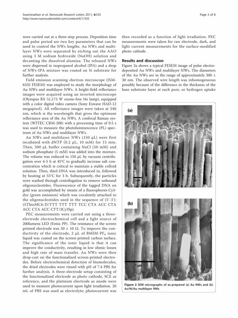
the as-prepared and dye-attached DNA-tagged Au andmultilayer NWs. From the optical investigation, the as-prepared NWs and multilayer NWs were suspended inIPA and water; its absorption spectra for different sam-ples were recorded. The surface plasmon band of metalparticles is most responsible for the degree of aggrega-tion and also sensitive to size and shape of the nanos-tructures. Major absorption peak was recorded at 540nm as prepared Au NWs (Figure 3a). Furthermore, itwas assigned to an interaction with a surface plasmonpolariton mode [20]. The Ni layer in multilayer struc-ture showed no reflection in the visible spectrum, whencompared with Au layers (Figure 3b). From Figure 3c,the maximum absorption peak shifted to 550 nm whichis because of the dye-attached DNA on Au NWs.The Au NWs were dispersed in different solvents:
water and IPA. Owing to different refractive index ofthe solvents, the reflected intensity of the plasmon bandvaries significantly with respect to the solvents. Hence,the optical absorbance of Au NWs in IPA is strongerthan that in water. It is anticipated that the surface plas-mon was dependent on the shape of the particles, thenature of the dispersing solvent, and the aggregation ofnanomaterials [14]. Therefore, the maximum opticalabsorption was observed for Au NWs, particularly dis-persed in IPA (Figure 3a). The absorption behavior wasdifferent, even though similar size of templates was used
for the synthesis of Au NWs and multilayer NWs. Theoptical absorbance was lower in multilayer NWsbecause of the amount of wire aggregation and the forceof attraction between the wires as Ni is a ferromagneticmaterial. An enhanced intensity of the plasmon withless aggregation can be obtained when suitable disper-sing solvent was used. In Au NWs, there is a minorshift in the absorbance band toward longer wavelengthsat 660 and 770 nm, which can be attributed to shapethe NWs and coupling between the Au NWs aggrega-tion [21].Figure 4 shows the optical reflectance and fluores-
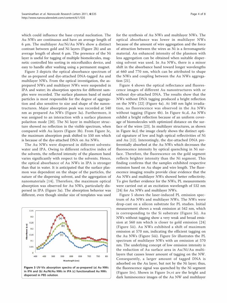
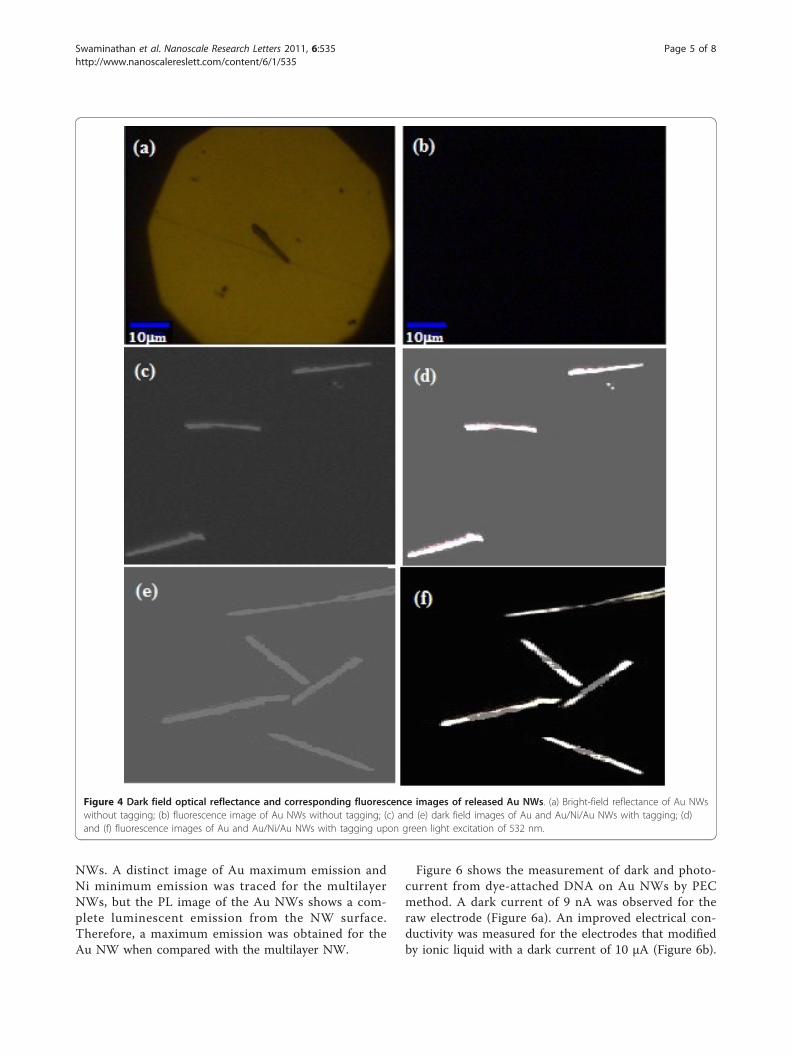
cence images of different Au nanostructures with orwithout dye-attached DNA. The results show that theNWs without DNA tagging produced a bright reflectionon the NWs [22] (Figure 4a). At 540 nm light irradia-tion, no fluorescence was observed in the Au NWswithout tagging (Figure 4b). In Figure 4c,d, Au NWsexhibit a bright reflection because of an uniform cover-age of biomolecules with optimized distance on the sur-face of the wires [23]. In multilayer structures, as shownin Figure 4e,f, the image clearly shows the distinct opti-cal signature of low and high optical reflectivities of Niand Au [12]. Interestingly, the dye-attached DNA pre-ferentially absorbed at the Au NWs which decreases thefluorescence intensity by optical quenching in Ni sur-face. Therefore, the fluorescence on the gold segmentreflects brighter intensity than the Ni segment. Thisfinding confirms that the samples exhibited respectiveemission based on Au shape and wire length. The fluor-escence imaging results provide clear evidence that theAu NWs and multilayer NWs showed better reflectivity.To give further evidence for the NWs, PL measurementswere carried out at an excitation wavelength of 532 nm[24] for Au NWs and multilayer NWs.Figure 5 shows the laser-induced PL emission spec-
trum of Au NWs and multilayer NWs. The NWs weredrop-cast on a silicon substrate for PL studies. Initialmeasurement shows a weak emission at 542 nm, whichis corresponding to the Si substrate (Figure 5i). AuNWs without tagging show a very weak and broad emis-sion at 560 nm which is closer to gold emission [24](Figure 5ii). Au NWs exhibited a shift of maximumemission at 570 nm, indicating the efficient tagging onthe Au NWs (Figure 5iii). Figure 5iv illustrates the PLspectrum of multilayer NWs with an emission at 570nm. The underlying concept of low emission intensity isthe reduction of Au surface area in Au/Ni/Au multi-layers that causes lesser amount of tagging on the NW.Consequently, a larger amount of tagged DNA isadsorbed on the Au layer, but not by the Ni layer; thus,the fluorescence signal was quenched by the Ni segment(Figure 5iv). Shown in Figure 5v,vi are the bright anddark luminescence images of the Au NW and multilayer
Figure 3 UV-Vis absorption spectra of as-prepared (a) Au NWsin IPA and (b) Au/Ni/Au NWs in IPA (c) functionalised Au NWsdispersed in PBS solution.
Swaminathan et al. Nanoscale Research Letters 2011, 6:535http://www.nanoscalereslett.com/content/6/1/535
Page 4 of 8
NWs. A distinct image of Au maximum emission andNi minimum emission was traced for the multilayerNWs, but the PL image of the Au NWs shows a com-plete luminescent emission from the NW surface.Therefore, a maximum emission was obtained for theAu NW when compared with the multilayer NW.
Figure 6 shows the measurement of dark and photo-current from dye-attached DNA on Au NWs by PECmethod. A dark current of 9 nA was observed for theraw electrode (Figure 6a). An improved electrical con-ductivity was measured for the electrodes that modifiedby ionic liquid with a dark current of 10 μA (Figure 6b).
Figure 4 Dark field optical reflectance and corresponding fluorescence images of released Au NWs. (a) Bright-field reflectance of Au NWswithout tagging; (b) fluorescence image of Au NWs without tagging; (c) and (e) dark field images of Au and Au/Ni/Au NWs with tagging; (d)and (f) fluorescence images of Au and Au/Ni/Au NWs with tagging upon green light excitation of 532 nm.
Swaminathan et al. Nanoscale Research Letters 2011, 6:535http://www.nanoscalereslett.com/content/6/1/535
Page 5 of 8
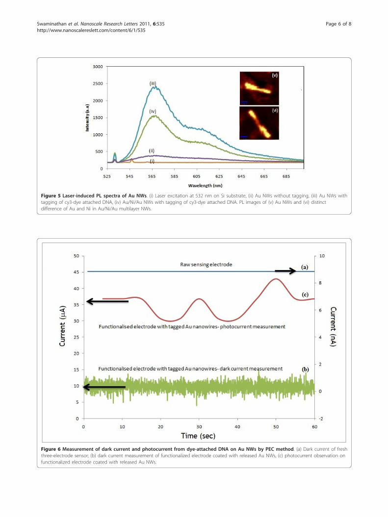
Figure 5 Laser-induced PL spectra of Au NWs. (i) Laser excitation at 532 nm on Si substrate, (ii) Au NWs without tagging, (iii) Au NWs withtagging of cy3-dye attached DNA, (iv) Au/Ni/Au NWs with tagging of cy3-dye attached DNA. PL images of (v) Au NWs and (vi) distinctdifference of Au and Ni in Au/Ni/Au multilayer NWs.
Figure 6 Measurement of dark current and photocurrent from dye-attached DNA on Au NWs by PEC method. (a) Dark current of freshthree-electrode sensor; (b) dark current measurement of functionalized electrode coated with released Au NWs, (c) photocurrent observation onfunctionalized electrode coated with released Au NWs.
Swaminathan et al. Nanoscale Research Letters 2011, 6:535http://www.nanoscalereslett.com/content/6/1/535
Page 6 of 8
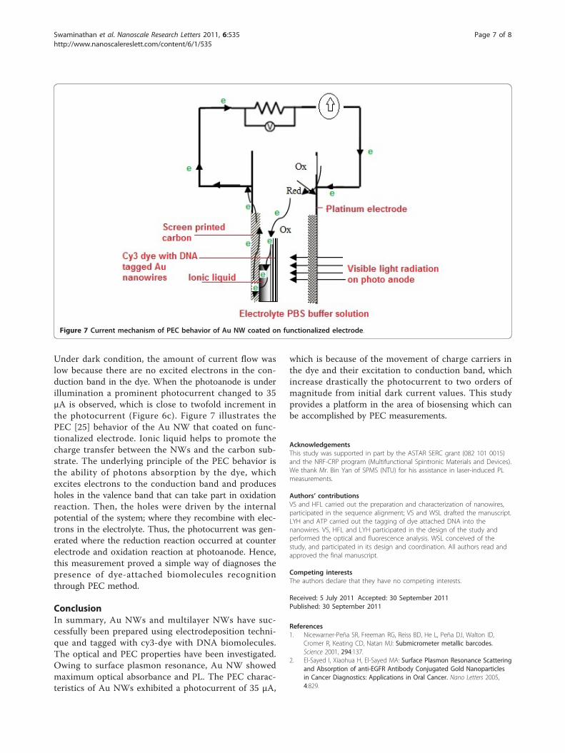
Under dark condition, the amount of current flow waslow because there are no excited electrons in the con-duction band in the dye. When the photoanode is underillumination a prominent photocurrent changed to 35μA is observed, which is close to twofold increment inthe photocurrent (Figure 6c). Figure 7 illustrates thePEC [25] behavior of the Au NW that coated on func-tionalized electrode. Ionic liquid helps to promote thecharge transfer between the NWs and the carbon sub-strate. The underlying principle of the PEC behavior isthe ability of photons absorption by the dye, whichexcites electrons to the conduction band and producesholes in the valence band that can take part in oxidationreaction. Then, the holes were driven by the internalpotential of the system; where they recombine with elec-trons in the electrolyte. Thus, the photocurrent was gen-erated where the reduction reaction occurred at counterelectrode and oxidation reaction at photoanode. Hence,this measurement proved a simple way of diagnoses thepresence of dye-attached biomolecules recognitionthrough PEC method.
ConclusionIn summary, Au NWs and multilayer NWs have suc-cessfully been prepared using electrodeposition techni-que and tagged with cy3-dye with DNA biomolecules.The optical and PEC properties have been investigated.Owing to surface plasmon resonance, Au NW showedmaximum optical absorbance and PL. The PEC charac-teristics of Au NWs exhibited a photocurrent of 35 μA,
which is because of the movement of charge carriers inthe dye and their excitation to conduction band, whichincrease drastically the photocurrent to two orders ofmagnitude from initial dark current values. This studyprovides a platform in the area of biosensing which canbe accomplished by PEC measurements.
AcknowledgementsThis study was supported in part by the ASTAR SERC grant (082 101 0015)and the NRF-CRP program (Multifunctional Spintronic Materials and Devices).We thank Mr. Bin Yan of SPMS (NTU) for his assistance in laser-induced PLmeasurements.
Authors’ contributionsVS and HFL carried out the preparation and characterization of nanowires,participated in the sequence alignment; VS and WSL drafted the manuscript.LYH and ATP carried out the tagging of dye attached DNA into thenanowires. VS, HFL and LYH participated in the design of the study andperformed the optical and fluorescence analysis. WSL conceived of thestudy, and participated in its design and coordination. All authors read andapproved the final manuscript.
Competing interestsThe authors declare that they have no competing interests.
Received: 5 July 2011 Accepted: 30 September 2011Published: 30 September 2011
References1. Nicewarner-Peña SR, Freeman RG, Reiss BD, He L, Peña DJ, Walton ID,
Cromer R, Keating CD, Natan MJ: Submicrometer metallic barcodes.Science 2001, 294:137.
2. El-Sayed I, Xiaohua H, El-Sayed MA: Surface Plasmon Resonance Scatteringand Absorption of anti-EGFR Antibody Conjugated Gold Nanoparticlesin Cancer Diagnostics: Applications in Oral Cancer. Nano Letters 2005,4:829.
Figure 7 Current mechanism of PEC behavior of Au NW coated on functionalized electrode.
Swaminathan et al. Nanoscale Research Letters 2011, 6:535http://www.nanoscalereslett.com/content/6/1/535
Page 7 of 8

3. Mirkin CA: Programming the assembly of two and three-dimensionalarchitectures with DNA and nanoscale inorganic building blocks. InorgChem 2000, 39:2258.
4. Baselt DR, Lee GL, Natesan M, Metzger SW, Sheehan PE, Colton RJ: Abiosensor based on magnetoresistance technology. Biosens Bioelectron1998, 13:731.
5. Peasley KW: Destruction of human immunodeficiency-infected cells byferrofluid substances into target cells. Med Hypothesis 1996, 46:5.
6. Reich DH, Tanase M, Hultgren A, Bauer LA, Chen CS, Meyer GJ: Biologicalapplications of multifunctional magnetic nanowires (invited). J Appl Phys2003, 93:7275.
7. El-Brolossy TA, Abdallah T, Mohamed MB, Abdallah S, Easawi K, Negm S,Talaat H: Shape and size dependence of the surface plasmon resonanceof gold nanoparticles studied by Photoacoustic technique. Eur Phys JSpecial Topics 2008, 153:361.
8. Kreibig U, Volmer M, Hilger A: Optical Properties of Metal Clusters.Springer, Germany; 1995:3:275.
9. Link S, El-Sayed MA: Spectral Properties and Relaxation Dynamics ofSurface Plasmon Electronic Oscillations in Gold and Silver Nanodots andNanorods. J Phys Chem B 1999, 103:8410.
10. Seong YL, Jae HK, Joon SL, Chan BP: Gold Nanoparticle EnlargementCoupled with Fluorescence Quenching for Highly Sensitive Detection ofAnalytes. Langmuir 2009, 25:13302-13305.
11. Nicewarner-Peña SR, Carado AJ, Shale KE, Keatin CD: Barcoded MetalNanowires: Optical Reflectivity and Patterned Fluorescence. J Phys ChemB 2003, 107:7360.
12. Mock JJ, Oldenburg SJ, Smith DR, Schultz DA, Schultz S: CompositePlasmon Resonant Nanowires. Nano Letters 2002, 2:465.
13. Martin CR: Membrane-Based Synthesis of Nanomaterials. Chem Mater1996, 8:1739.
14. Reiss BD, Freeman RG, Walton ID, Norton SM, Smith PC, Stonas WG,Keating CD, Natan MJ: Electrochemical synthesis and optical readout ofstriped metal rods with submicron features. J Electroanal Chem 2002,522:95.
15. Xu CL, Zhang L, Zhang HL, Li HL: Well-dispersed gold nanowiresuspension for assembly application. Appl Surf Sci 2005, 252:1182.
16. Sokolov K, Chumanov G, Cotton TM: Enhancement of MolecularFluorescence near the Surface of Colloidal Metal Films. Anal Chem 1998,70:3898.
17. Martin BR, Angelo SKS, Mallouk TE: Interactions Between SuspendedNanowires and Patterned Surface. Adv Funct Mater 2002, 12:759.
18. Nan J, Weidong R, Chunxu W, Zhicheng Lu, Bing Z: Fabrication of SilverDecorated Anodic Aluminum Oxide Substrate and Its Optical Propertieson Surface-Enhanced Raman Scattering and Thin Film Interference.Langmuir 2009, 25:11869-11873.
19. Iuliana ES, Megan EW, Robert MC: Fabrication of Silica-Coated GoldNanorods Functionalized with DNA for Enhanced Surface PlasmonResonance Imaging Biosensing Applications. Langmuir 2009,25:11282-11284.
20. Doremus RH: Optical Properties of Small Gold Particles. J Chem Phys 1964,40:2389.
21. Lee JH, Wu JH, Liu HL, Cho JU, Cho MK, An BH, Min JH, Noh SJ, Kim YK:Iron-Gold Barcode Nanowires. Angew Chem 2007, 119:3737.
22. Chen Y, Munechika K, Ginger DS: Dependence of Fluorescence Intensityon the Spectral Overlap between Fluorophores and Plasmon ResonantSingle Silver Nanoparticles. NanoLetters 2007, 7:690.
23. Stoermer RL, Sioss JA, Keating CD: Stabilization of Silver Metal in CitrateBuffer: Barcoded Nanowires and Their Bioconjugates. Chem Mater 2005,17:4356.
24. Clayton DA, Benoist DM, Zhu Y, Pan S: Photoluminescence andSpectroelectrochemistry of Single Ag Nanowires. ACS Nano 2010, 4:2363.
25. Hafeman DG, Parce JW, McConnell HM: Light-addressable potentiometricsensor for biochemical systems. Science 1988, 240:1182.
doi:10.1186/1556-276X-6-535Cite this article as: Swaminathan et al.: Photoelectrochemical studies ofDNA-tagged biomolecules on Au and Au/Ni/Au multilayer nanowires.Nanoscale Research Letters 2011 6:535.
Submit your manuscript to a journal and benefi t from:
7 Convenient online submission
7 Rigorous peer review
7 Immediate publication on acceptance
7 Open access: articles freely available online
7 High visibility within the fi eld
7 Retaining the copyright to your article
Submit your next manuscript at 7 springeropen.com
Swaminathan et al. Nanoscale Research Letters 2011, 6:535http://www.nanoscalereslett.com/content/6/1/535
Page 8 of 8