Placement and Routing in Computer Aided Design of Standard ...
Placement and Routing for Power Module Layout
Tristan Evans, Prof. Yarui Peng, & Prof. Alan Mantooth
University of Arkansas
Paper No: S3P1

Outline
• Motivation
• PowerSynth Introduction• Overview
• Improvement
• Placement & Routing for Power Electronics• VLSI Inspiration
• Force-Directed Placement
• Grid-Based Routing
• Initial Results
• Conclusions and Future Work

Power Electronics is EverywhereELECTRIC GENERATION
CO
MM
ER
CIA
L
RESIDENTIAL
IND
US
TR
IAL

MCPM Co-Design Challenges
Physical design of multi-chip power modules(MCPM) is time consuming and poses severalchallenges:
oMulti-domain nature of power electronic packaging necessitates consideration of materials and designs towards reduced: oElectrical parasitics for high performance devices
o Temperature and mechanical stress for higherreliability
oTraditional design flows are iterative and require extensive use of computationally expensive finite element analysis (FEA)

PowerSynth Overview• EDA tool for multi-chip power modules
(MCPM)• Multi-objective layout optimization• Reduced order models• Pareto-front of tradeoffs• Design export
Tristan M. Evans, Quang Le, Shilpi Mukherjee, Imam Al Razi, Tom Vrotsos,
Yarui Peng, H. Alan Mantooth , "PowerSynth: A Power Module Layout
Generation Tool," in IEEE Transactions on Power Electronics, vol. 34, no. 6, pp.
5063-5078, June 2019. doi: 10.1109/TPEL.2018.2870346 Highlighted Paper

PowerSynth Manufacturer Design Kit (MDK) and Technology Library
Layer Stack
• Input file describing layers and technologies
• Holds information pertaining to
• Layer width, length, andthickness
• Layer material properties
Illustration of design rules pertaining to
feature placement and minimum
spacing
MDK and Design Rules and
Checker (DRC)
• Input file containing
technology-dependent design
and processing rules
• Ensures feature sizing and
component placement are
within processing tolerance
MCPM layer stack
Trace Trace
Substrate
Metal
Baseplate
0.22
0.41
0.64
0.41
6.0
Min spacing
1.2
Min width
1.2
Min enclosure
0.2Device
Thickness
PowerSynth technology library wizard

PowerSynth Layout Engine
▪ Constraint aware, hierarchical layout engine
▪ Minimum trace gaps set by trace-to-trace potential difference
▪ Heterogeneous component support
▪ Fixed or minimum layout size capabilities
Initial Design
PowerSynth Input Minimum Size
I. Al Razi, Q. Le, H. A. Mantooth, and Y. Peng, “Constraint-Aware Algorithms for Heterogeneous Power
Module Layout Synthesis and Reliability Optimization.” in 2018 IEEE 6th Workshop on Wide Bandgap Power
Devices and Applications (WiPDA), 2018, pp. 323-330.
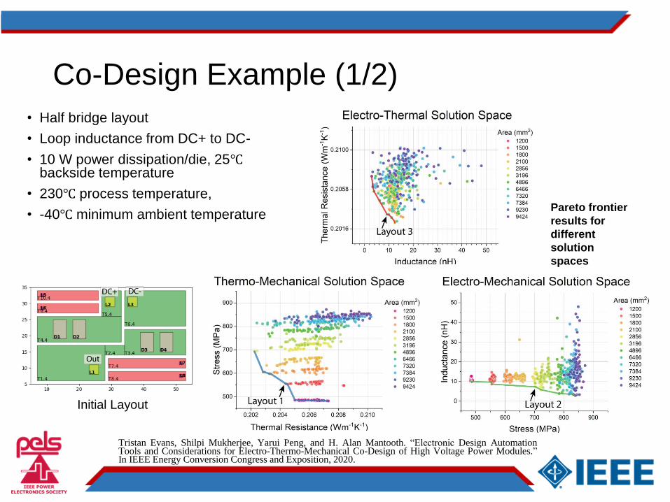
Co-Design Example (1/2)
• Half bridge layout
• Loop inductance from DC+ to DC-
• 10 W power dissipation/die, 25℃backside temperature
• 230℃ process temperature,
• -40℃ minimum ambient temperature
Initial Layout
Pareto frontier
results for
different
solution
spaces
Tristan Evans, Shilpi Mukherjee, Yarui Peng, and H. Alan Mantooth. “Electronic Design AutomationTools and Considerations for Electro-Thermo-Mechanical Co-Design of High Voltage Power Modules.”In IEEE Energy Conversion Congress and Exposition, 2020.
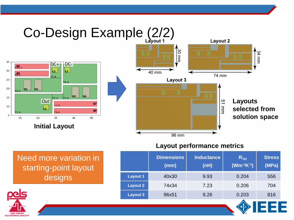
Co-Design Example (2/2)
Dimensions
(mm)
Inductance
(nH)
RTH
(Wm-1K-1)
Stress
(MPa)
Layout 1 40x30 9.93 0.204 556
Layout 2 74x34 7.23 0.206 704
Layout 3 96x51 9.26 0.203 816
Layouts
selected from
solution space
Layout performance metrics
Initial Layout
Need more variation in
starting-point layout
designs
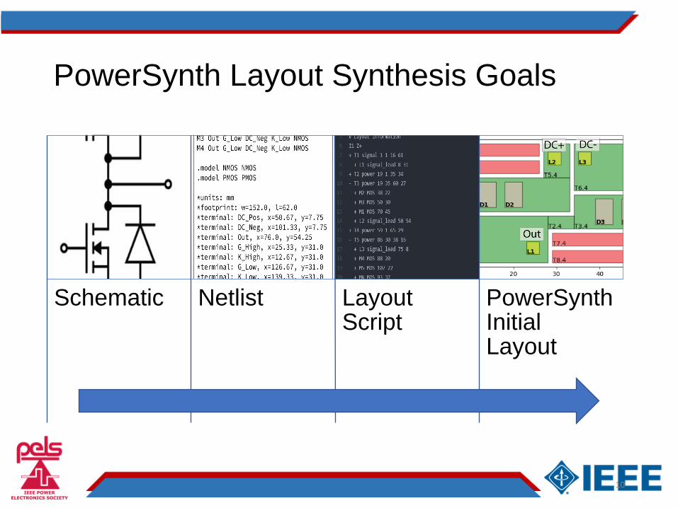
PowerSynth Layout Synthesis Goals
10
Schematic Netlist Layout Script
PowerSynth Initial Layout

From Very Large-Scale Integration (VLSI) to Power Electronics (1/3)
11
VLSI Layout
Power Module Layout
Component Count
High (up to billions)
Low (generally <20 )
Component Dimensions
Regular Irregular
Routing Layers
Multiple Single, Multiple (gaining traction)
Primary Fitness Metrics
Footprint, timing delay
Footprint, electrical parasitics,junction temperature, mechanical stress
Typical power module topologies
VLSI vs. Power Layout Aspects

From VLSI to Power Electronics (2/3)
12
Typical VLSI design flow
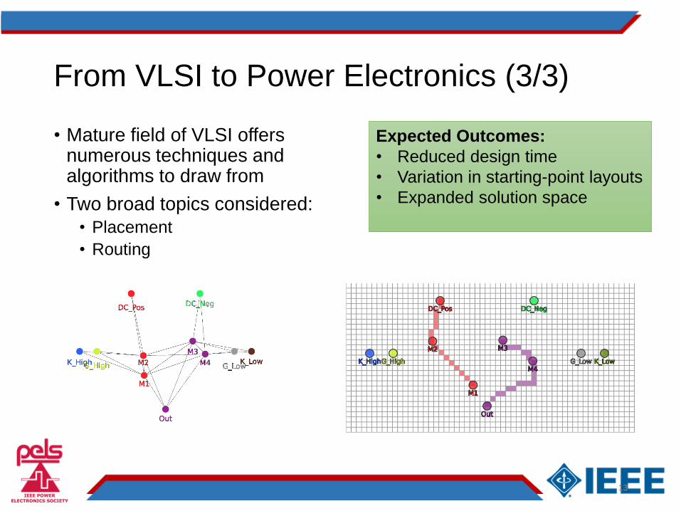
From VLSI to Power Electronics (3/3)
• Mature field of VLSI offers numerous techniques and algorithms to draw from
• Two broad topics considered:
• Placement
• Routing
13
Expected Outcomes:
• Reduced design time
• Variation in starting-point layouts
• Expanded solution space

Power Module Place-and-Route
14

Annotated Netlist Input
• Specification of additional parameters for aiding layout synthesis
• Properties include:• Terminal names as nodes
with locations specified
• Overall footprint
• Units
• Device Kelvin connection
• Parsed netlist used for placement and routing
15
Half-bridge annotated netlist example

Force-Directed Placement
16
𝐹 = −𝑘Δ𝑠
𝐹 = −𝑘 logΔ𝑠
𝑐
Design Variables:• Initial device position
• Mass
• Damping
• Spring coefficients
• Spring rest length
Governing Equations:
Attractive:
Repulsive:
Attractive Forces Repulsive Forces
Device-Device (in-group) Device-Device (out-group)
Device-Terminal (connected) Device-Boundary
Spring Force Assignment
Neil R. Quinn, Melvin A. Breuer, “A Forced Directed Component Placement
Procedure for Printed Circuit Boards,” IEEE Transactions on Circuits and
Systems, 26(6):377-388 1979
Ref:
Illustration of spring
forces among
devices and
terminals
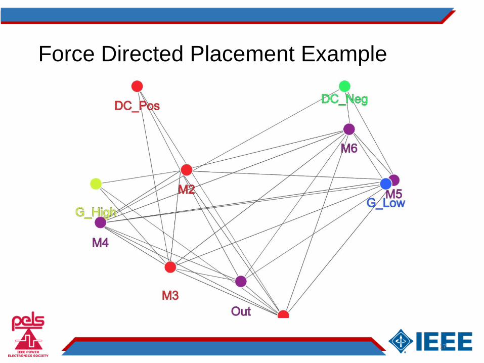
Force Directed Placement Example
17
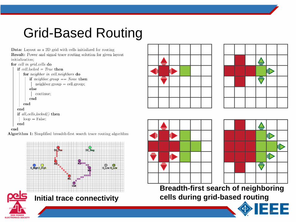
Grid-Based Routing
18
Breadth-first search of neighboring
cells during grid-based routingInitial trace connectivity

Routing Example
19

Initial Results Example
20
Placement Routing
Finalized layoutLayout in PowerSynth
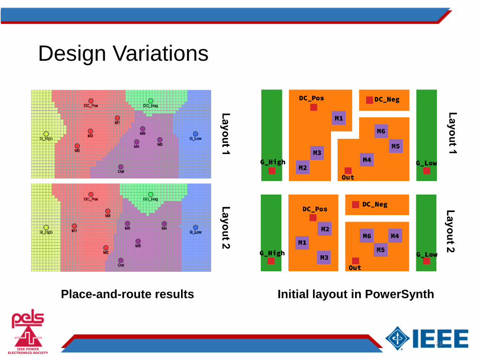
Design Variations
21
Place-and-route results Initial layout in PowerSynth

Caveats and Future Work
• Limitations• Many assumptions have been made, including:
• Planar, 2D structures
• Vertical devices
• Bondwire overlap
• Prototype implementation• Not optimized for speed
• Naïve
• Further Development• Validate hypothesis with case studies
• Fully automate export
• Expand capabilities into multi-layer, heterogeneous structures
22

Summary
• PowerSynth is an EDA tool for power module layout under active development
• PowerSynth models and optimization results have been validated, but more work needs to be done to expand the solution space it produces
• VLSI techniques have been applied toward the placement and routing of components from a netlist starting point
• These features will be incorporated in PowerSynth and case studies performed to evaluate and refine the approach
23
Thank you!
24