NuMicro Family NUC121/125 Series Datasheet - Nuvoton · NuMicro® Family NUC121/125 Series...
150
NUC121/125 Feb. 23, 2017 Page 1 of 150 Rev 1.00 NUC121/125 SERIES DATASHEET ARM Cortex ® -M0 32-bit Microcontroller NuMicro ® Family NUC121/125 Series Datasheet The information described in this document is the exclusive intellectual property of Nuvoton Technology Corporation and shall not be reproduced without permission from Nuvoton. Nuvoton is providing this document only for reference purposes of NuMicro microcontroller based system design. Nuvoton assumes no responsibility for errors or omissions. All data and specifications are subject to change without notice. For additional information or questions, please contact: Nuvoton Technology Corporation. www.nuvoton.com
Transcript of NuMicro Family NUC121/125 Series Datasheet - Nuvoton · NuMicro® Family NUC121/125 Series...
NUC121/125
Feb. 23, 2017 Page 1 of 150 Rev 1.00
NU
C12
1/1
25 S
ER
IES
DA
TA
SH
EE
T
ARM Cortex®-M0
32-bit Microcontroller
NuMicro® Family
NUC121/125 Series
Datasheet
The information described in this document is the exclusive intellectual property of Nuvoton Technology Corporation and shall not be reproduced without permission from Nuvoton.
Nuvoton is providing this document only for reference purposes of NuMicro microcontroller based system design. Nuvoton assumes no responsibility for errors or omissions.
All data and specifications are subject to change without notice.
For additional information or questions, please contact: Nuvoton Technology Corporation.
www.nuvoton.com
NUC121/125
Feb. 23, 2017 Page 2 of 150 Rev 1.00
NU
C12
1/1
25 S
ER
IES
DA
TA
SH
EE
T
TABLE OF CONTENTS
1 GENERAL DESCRIPTION ...................................................................... 9
Key Features Support Table ......................................................................... 9 1.1
2 FEATURES .......................................................................................10
NuMicro® NUC121/125 Features ................................................................... 10 2.1
3 Abbreviations ....................................................................................16
Abbreviations .......................................................................................... 16 3.1
4 PARTS INFORMATION LIST AND PIN CONFIGURATION .............................18
NuMicro® NUC121/125 Selection Guide .......................................................... 18 4.1
4.1.1 NuMicro® NUC121/125 Naming Rule ..................................................................... 18
4.1.2 NuMicro® NUC121 USB Series Selection Guide ........................................................ 19
4.1.3 NuMicro® NUC125 USB Series Selection Guide ........................................................ 19
Pin Configuration ...................................................................................... 20 4.2
4.2.1 NuMicro® NUC121 QFN 33-Pin Diagram ................................................................. 20
4.2.2 NuMicro® NUC121 QFN 33-Pin Function Diagram ...................................................... 21
4.2.3 NuMicro® NUC121 LQFP 48-Pin Diagram ................................................................ 22
4.2.4 NuMicro® NUC121 LQFP 48-Pin Function Diagram .................................................... 23
4.2.5 NuMicro® NUC121 LQFP 64-Pin Diagram ................................................................ 24
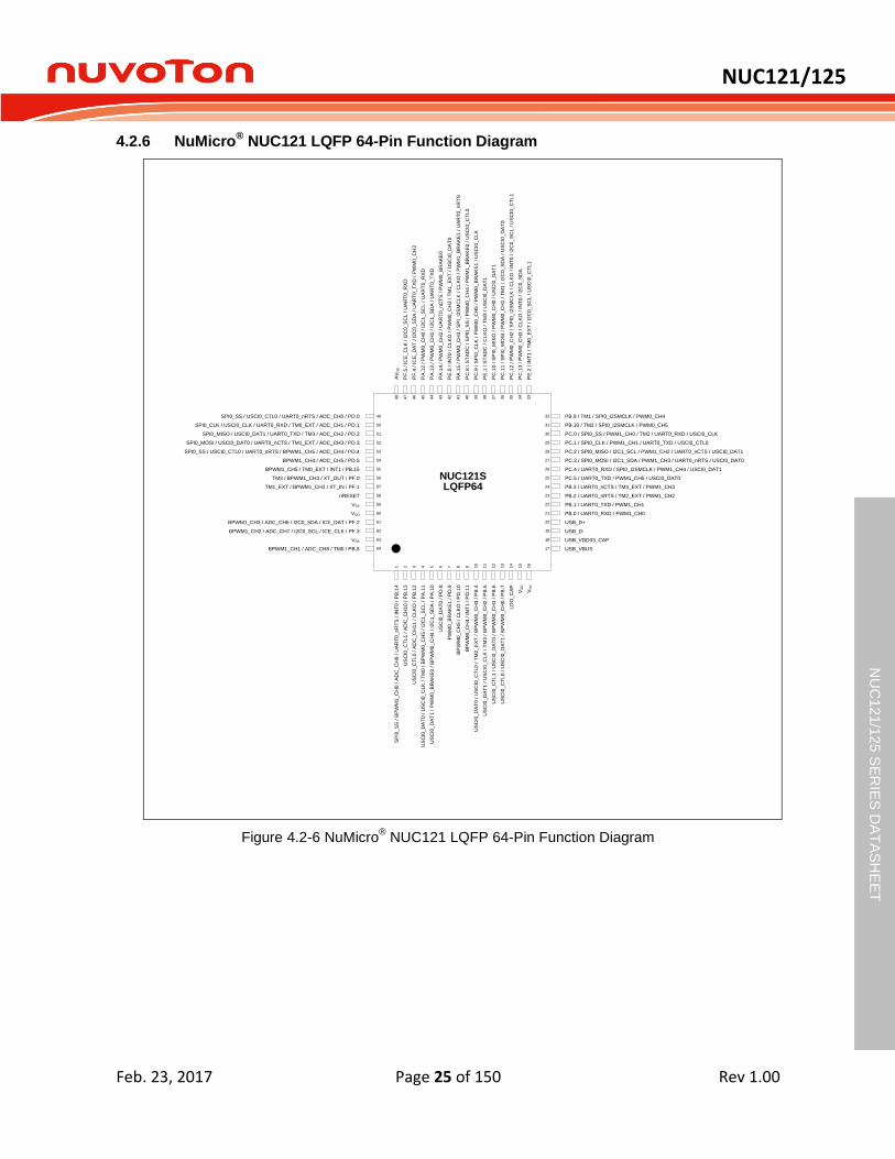
4.2.6 NuMicro® NUC121 LQFP 64-Pin Function Diagram .................................................... 25
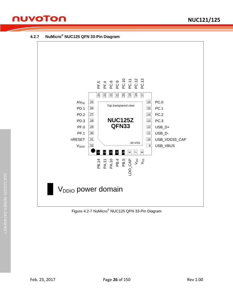
4.2.7 NuMicro® NUC125 QFN 33-Pin Diagram ................................................................. 26
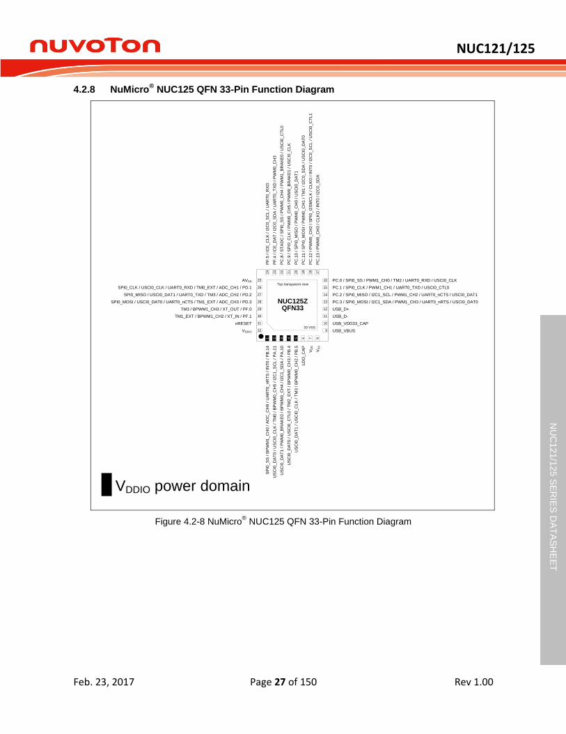
4.2.8 NuMicro® NUC125 QFN 33-Pin Function Diagram ...................................................... 27
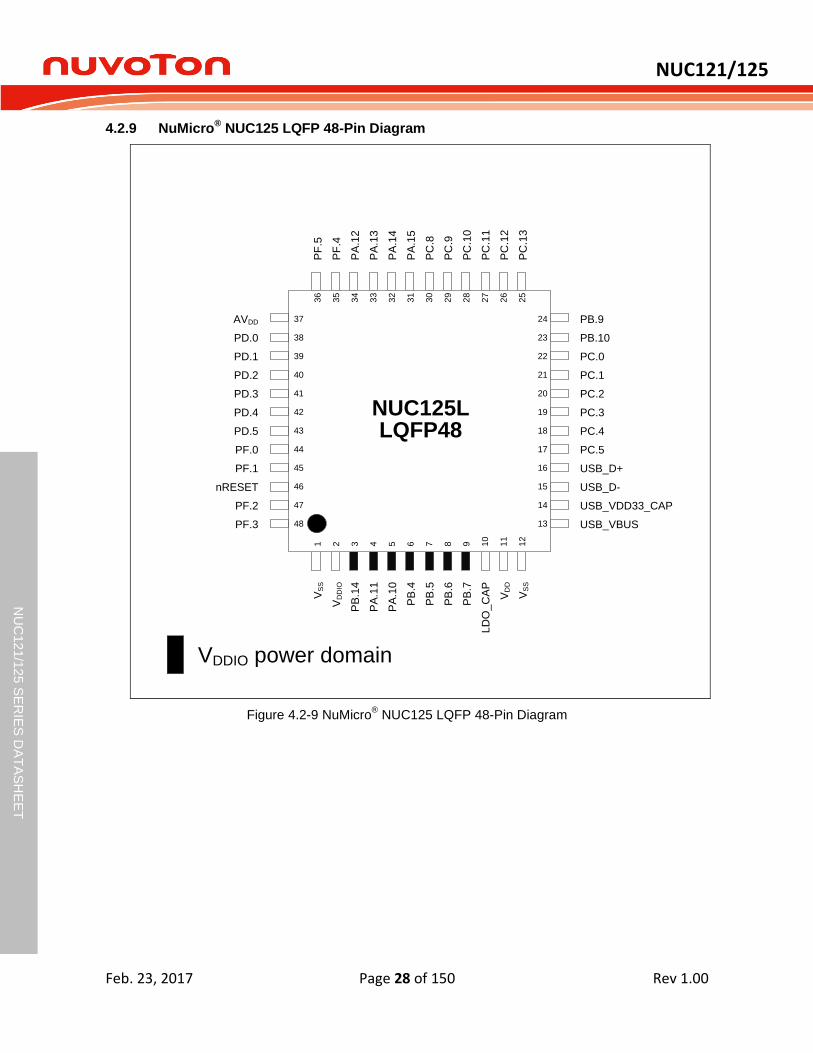
4.2.9 NuMicro® NUC125 LQFP 48-Pin Diagram ................................................................ 28
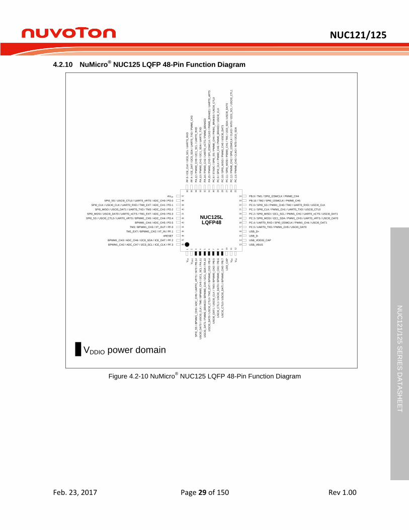
4.2.10 NuMicro® NUC125 LQFP 48-Pin Function Diagram .................................................... 29
4.2.11 NuMicro® NUC125 LQFP 64-Pin Diagram ................................................................ 30
4.2.12 NuMicro® NUC125 LQFP 64-Pin Function Diagram .................................................... 31
Pin Description ........................................................................................ 32 4.3
4.3.1 NUC121 USB Series QFN33 Pin Description ............................................................ 32
4.3.2 NUC121 USB Series LQFP48 Pin Description .......................................................... 37
4.3.3 NUC121 USB Series LQFP64 Pin Description .......................................................... 44
4.3.4 NUC125 USB Series QFN33 Pin Description ............................................................ 52
4.3.5 NUC125 USB Series LQFP48 Pin Description .......................................................... 57
4.3.6 NUC125 USB Series LQFP64 Pin Description .......................................................... 64
4.3.7 GPIO Multi-function Pin Summary ......................................................................... 72
5 BLOCK DIAGRAM ..............................................................................78
NUC121/125
Feb. 23, 2017 Page 3 of 150 Rev 1.00
NU
C12
1/1
25 S
ER
IES
DA
TA
SH
EE
T
NuMicro® NUC121/125 Block Diagram ............................................................ 78 5.1
6 FUNCTIONAL DESCRIPTION ................................................................79
ARM® Cortex® -M0 Core .............................................................................. 79 6.1
System Manager ...................................................................................... 81 6.2
6.2.1 Overview ....................................................................................................... 81
6.2.2 System Reset.................................................................................................. 81
6.2.3 Power Modes and Wake-up Sources ...................................................................... 88
6.2.4 System Power Distribution .................................................................................. 90
Clock Controller ....................................................................................... 92 6.3
6.3.1 Overview ....................................................................................................... 92
6.3.2 Clock Generator ............................................................................................... 94
6.3.3 System Clock and SysTick Clock .......................................................................... 96
6.3.4 Peripherals Clock ............................................................................................. 98
6.3.5 Power-down Mode Clock .................................................................................... 98
6.3.6 Clock Output ................................................................................................... 98
Flash Memory Controller (FMC) .................................................................. 100 6.4
6.4.1 Overview ..................................................................................................... 100
6.4.2 Features ...................................................................................................... 100
General Purpose I/O (GPIO) ...................................................................... 101 6.5
6.5.1 Overview ..................................................................................................... 101
6.5.2 Features ...................................................................................................... 101
PDMA Controller (PDMA) ......................................................................... 102 6.6
6.6.1 Overview ..................................................................................................... 102
6.6.2 Features ...................................................................................................... 102
Timer Controller (TMR) ............................................................................ 103 6.7
6.7.1 Overview ..................................................................................................... 103
6.7.2 Features ...................................................................................................... 103
Basic PWM Generator and Capture Timer (BPWM) .......................................... 104 6.8
6.8.1 Overview ..................................................................................................... 104
6.8.2 Features ...................................................................................................... 104
PWM Generator and Capture Timer (PWM) ................................................... 105 6.9
6.9.1 Overview ..................................................................................................... 105
6.9.2 Features ...................................................................................................... 105
Watchdog Timer (WDT)............................................................................ 107 6.10
NUC121/125
Feb. 23, 2017 Page 4 of 150 Rev 1.00
NU
C12
1/1
25 S
ER
IES
DA
TA
SH
EE
T
6.10.1 Overview ..................................................................................................... 107
6.10.2 Features ...................................................................................................... 107
Window Watchdog Timer (WWDT) .............................................................. 108 6.11
6.11.1 Overview ..................................................................................................... 108
6.11.2 Features ...................................................................................................... 108
USCI - Universal Serial Control Interface Controller .......................................... 109 6.12
6.12.1 Overview ..................................................................................................... 109
6.12.2 Features ...................................................................................................... 109
USCI - UART Mode ................................................................................ 110 6.13
6.13.1 Overview ..................................................................................................... 110
6.13.2 Features ...................................................................................................... 110
USCI - SPI Mode .................................................................................... 111 6.14
6.14.1 Overview ..................................................................................................... 111
6.14.2 Features ...................................................................................................... 111
USCI - I2C Mode .................................................................................... 113 6.15
6.15.1 Overview ..................................................................................................... 113
6.15.2 Features ...................................................................................................... 113
UART Interface Controller (UART) ............................................................... 114 6.16
6.16.1 Overview ..................................................................................................... 114
6.16.2 Features ...................................................................................................... 114
I2C Serial Interface Controller (I2C) .............................................................. 116 6.17
6.17.1 Overview ..................................................................................................... 116
6.17.2 Features ...................................................................................................... 116
Serial Peripheral Interface (SPI) .................................................................. 117 6.18
6.18.1 Overview ..................................................................................................... 117
6.18.2 Features ...................................................................................................... 117
USB Device Controller (USBD) ................................................................... 118 6.19
6.19.1 Overview ..................................................................................................... 118
6.19.2 Features ...................................................................................................... 118
Analog-to-Digital Converter (ADC) ............................................................... 119 6.20
6.20.1 Overview ..................................................................................................... 119
6.20.2 Features ...................................................................................................... 119
7 APPLICATION CIRCUIT ..................................................................... 120
8 ELECTRICAL CHARACTERISTICS ....................................................... 122
NUC121/125
Feb. 23, 2017 Page 5 of 150 Rev 1.00
NU
C12
1/1
25 S
ER
IES
DA
TA
SH
EE
T
Absolute Maximum Ratings ....................................................................... 122 8.1
DC Electrical Characteristics ...................................................................... 123 8.2
AC Electrical Characteristics ...................................................................... 131 8.3
8.3.1 External 4~24 MHz High Speed Crystal (HXT) Input Clock .......................................... 131
8.3.2 External 4~24 MHz High Speed Crystal (HXT) Oscillator ............................................ 131
8.3.3 External 32.768 kHz Low Speed Crystal (LXT) Input Clock ......................................... 132
8.3.4 External 32.768 kHz Low Speed Crystal (LXT) Oscillator ............................................ 132
Analog Characteristics ............................................................................. 135 8.4
8.4.1 12-bit ADC ................................................................................................... 135
8.4.2 LDO ........................................................................................................... 137
8.4.3 Low-Voltage Reset ......................................................................................... 137
8.4.4 Brown-out Detector ......................................................................................... 137
8.4.5 Power-on Reset ............................................................................................. 138
8.4.6 Temperature Sensor ....................................................................................... 139
8.4.7 USB PHY ..................................................................................................... 140
Flash DC Electrical Characteris .................................................................. 141 8.5
I2C Dynamic Characteristics ...................................................................... 142 8.6
SPI Dynamic Characteristics ...................................................................... 143 8.7
8.7.1 Dynamic Characteristics of Data Input and Output Pin ............................................... 143
9 PACKAGE DIMENSIONS .................................................................... 145
LQFP 64S (7x7x1.4 mm) .......................................................................... 145 9.1
LQFP 48L (7x7x1.4 mm) .......................................................................... 146 9.2
QFN 33Z (5x5x0.8 mm) ............................................................................ 147 9.3
10 REVISION HISTORY .......................................................................... 149
NUC121/125
Feb. 23, 2017 Page 6 of 150 Rev 1.00
NU
C12
1/1
25 S
ER
IES
DA
TA
SH
EE
T
List of Figures
Figure 4.1-1 NuMicro® NUC121/125 Selection Code .................................................................... 18
Figure 4.2-1 NuMicro® NUC121 QFN 33-Pin Diagram .................................................................. 20
Figure 4.2-2 NuMicro® NUC121 QFN 33-Pin Function Diagram ................................................... 21
Figure 4.2-3 NuMicro® NUC121 LQFP 48-Pin Diagram ................................................................ 22
Figure 4.2-4 NuMicro® NUC121 LQFP 48-Pin Function Diagram ................................................. 23
Figure 4.2-5 NuMicro® NUC121 LQFP 64-Pin Diagram ................................................................ 24
Figure 4.2-6 NuMicro® NUC121 LQFP 64-Pin Function Diagram ................................................. 25
Figure 4.2-7 NuMicro® NUC125 QFN 33-Pin Diagram .................................................................. 26
Figure 4.2-8 NuMicro® NUC125 QFN 33-Pin Function Diagram ................................................... 27
Figure 4.2-9 NuMicro® NUC125 LQFP 48-Pin Diagram ................................................................ 28
Figure 4.2-10 NuMicro® NUC125 LQFP 48-Pin Function Diagram ............................................... 29
Figure 4.2-11 NuMicro® NUC125 LQFP 64-Pin Diagram .............................................................. 30
Figure 4.2-12 NuMicro® NUC125 LQFP 64-Pin Function Diagram ............................................... 31
Figure 5.1-1 NuMicro® NUC121/125 Block Diagram ..................................................................... 78
Figure 6.1-1 Cortex®-M0 Block Diagram ........................................................................................ 79
Figure 6.2-1 System Reset Sources .............................................................................................. 82
Figure 6.2-2 nRESET Reset Waveform ......................................................................................... 85
Figure 6.2-3 Power-on Reset (POR) Waveform ............................................................................ 85
Figure 6.2-4 Low Voltage Reset (LVR) Waveform ......................................................................... 86
Figure 6.2-5 Brown-out Detector (BOD) Waveform ....................................................................... 87
Figure 6.2-6 Power Mode State Machine ...................................................................................... 88
Figure 6.2-7 NuMicro® NUC121/125 Power Distribution Diagram ................................................. 91
Figure 6.3-1 Clock Generator Global View Diagram ...................................................................... 93
Figure 6.3-2 Clock Generator Block Diagram ................................................................................ 95
Figure 6.3-3 System Clock Block Diagram .................................................................................... 96
Figure 6.3-4 HXT Stop Protect Procedure ..................................................................................... 97
Figure 6.3-5 SysTick Clock Control Block Diagram ....................................................................... 98
Figure 6.3-6 Clock Source of Clock Output ................................................................................... 99
Figure 6.3-7 Clock Output Block Diagram ..................................................................................... 99
Figure 6.14-1 SPI Master Mode Application Block Diagram ........................................................ 111
Figure 6.14-2 SPI Slave Mode Application Block Diagram .......................................................... 111
Figure 6.15-1 I2C Bus Timing ....................................................................................................... 113
Figure 8.3-1 Typical Crystal Application Circuit ........................................................................... 132
Figure 8.3-2 Typical Crystal Application Circuit ........................................................................... 133
Figure 8.4-1 Power-up Ramp Condition ...................................................................................... 138
NUC121/125
Feb. 23, 2017 Page 7 of 150 Rev 1.00
NU
C12
1/1
25 S
ER
IES
DA
TA
SH
EE
T
Figure 8.6-1 I2C Timing Diagram ................................................................................................. 142
Figure 8.7-1 SPI Master Mode Timing Diagram .......................................................................... 143
Figure 8.7-2 SPI Slave Mode Timing Diagram ............................................................................ 144
NUC121/125
Feb. 23, 2017 Page 8 of 150 Rev 1.00
NU
C12
1/1
25 S
ER
IES
DA
TA
SH
EE
T
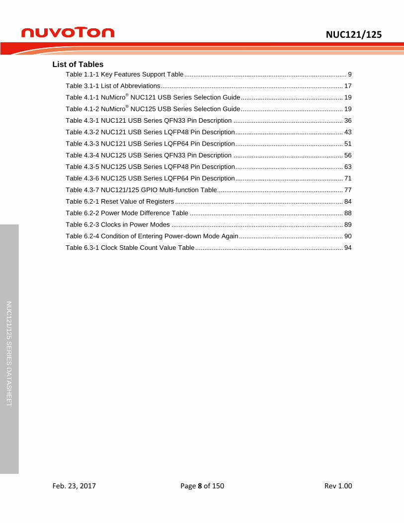
List of Tables
Table 1.1-1 Key Features Support Table ......................................................................................... 9
Table 3.1-1 List of Abbreviations .................................................................................................... 17
Table 4.1-1 NuMicro® NUC121 USB Series Selection Guide ........................................................ 19
Table 4.1-2 NuMicro® NUC125 USB Series Selection Guide ........................................................ 19
Table 4.3-1 NUC121 USB Series QFN33 Pin Description ............................................................ 36
Table 4.3-2 NUC121 USB Series LQFP48 Pin Description ........................................................... 43
Table 4.3-3 NUC121 USB Series LQFP64 Pin Description ........................................................... 51
Table 4.3-4 NUC125 USB Series QFN33 Pin Description ............................................................ 56
Table 4.3-5 NUC125 USB Series LQFP48 Pin Description ........................................................... 63
Table 4.3-6 NUC125 USB Series LQFP64 Pin Description ........................................................... 71
Table 4.3-7 NUC121/125 GPIO Multi-function Table..................................................................... 77
Table 6.2-1 Reset Value of Registers ............................................................................................ 84
Table 6.2-2 Power Mode Difference Table .................................................................................... 88
Table 6.2-3 Clocks in Power Modes .............................................................................................. 89
Table 6.2-4 Condition of Entering Power-down Mode Again ......................................................... 90
Table 6.3-1 Clock Stable Count Value Table ................................................................................. 94

NUC121/125
Feb. 23, 2017 Page 9 of 150 Rev 1.00
NU
C12
1/1
25 S
ER
IES
DA
TA
SH
EE
T
1 GENERAL DESCRIPTION
The NuMicro® NUC121/125 series is a 32-bit Cortex
®-M0 microcontroller with USB 2.0 Full-speed
device, a 12-bit ADC and 4 sets of 6-channel BPWM. The NUC121/125 series provides the high 50 MHz operating speed, 8 Kbytes SRAM, 8 USB endpoints and 24 channels of BPWM, which make it powerful in USB communication and data processing. The NUC121/125 series is ideal for industrial control, consumer electronics, and communication system applications such as printers, touch panel, gaming keyboard, gaming joystick, USB audio, PC peripherals, and alarm systems.
The NUC121/125 series runs up to 50 MHz and supports 32-bit multiplier, structure NVIC (Nested Vector Interrupt Control), dual-channel APB and PDMA (Peripheral Direct Memory Access) with CRC function. Besides, the NUC121/125 series is equipped with 32 Kbytes Flash memory, 8 Kbytes SRAM, and 4 Kbytes loader ROM for the ISP. It operates at a wide voltage range of 2.5V
~ 5.5V and temperature range of -40℃ ~ +105℃. It is also equipped with plenty of peripheral
devices, such as 8-channel 12-bit ADC, USCI, UART, SPI, I2C, I
2S, USB 2.0 FS device, and
offers low-voltage reset and Brown-out detection, PWM (Pulse-width Modulation), capture and compare features, four sets of 32-bit timers, Watchdog Timer, and internal RC oscillator. All these peripherals have been incorporated into the NUC121/125 series to reduce component count, board space and system cost.
Additionally, the NUC121/125 series is equipped with ISP (In-System Programming), IAP (In-Application-Programming) and ICP (In-Circuit Programming) functions, which allows the user to update the program under software control through the on-chip connectivity interface, such as SWD, UART and USB. Also all series support SPROM. Moreover, the NUC125 support Voltage Adjustable Interface with individual I/O (1.8V-5.5V) for saving additional cost on adjusting the interface voltage difference of peripheral components.
Key Features Support Table 1.1
* USCI can be set to UART, I2C or SPI
Product Line USBD USCI UART I2C SPI/ I
2S Timer BPWM ADC
NUC121 1 1 1 2 1 4 24 12
NUC125 1 1 1 2 1 4 23 11
Table 1.1-1 Key Features Support Table
The NuMicro® NUC121/125 series is suitable for a wide range of applications such as:
USB Keyboard / Mouse
Gaming - Joystick
Industrial Automation
Home Automation
VR peripheral application
USB audio
Alarm system
NUC121/125
Feb. 23, 2017 Page 10 of 150 Rev 1.00
NU
C12
1/1
25 S
ER
IES
DA
TA
SH
EE
T
2 FEATURES
NuMicro® NUC121/125 Features 2.1
Core
– ARM® Cortex® -M0 core running up to 50 MHz – One 24-bit system timer – Supports Low Power Sleep mode – Single-cycle 32-bit hardware multiplier – Supports programmable 4 level priorities of Nested Vectored Interrupt Controller
(NVIC) – Supports programmable mask-able interrupts – Supports Serial Wire Debug(SWD) with 2 watch-points/4 breakpoints
Built-in LDO for wide operating voltage ranged from 2.5V to 5.5V
Flash Memory
– Supports 32 KB application ROM (APROM) – Supports 4.5 KB Flash for loader (LDROM) – Supports 512 bytes Security Protection Rom (SPROM) – Supports 12 bytes User Configuration block to control system initiation – Supports Data Flash with configurable memory size – Supports 512 bytes page erase for all embedded flash – Supports In-System-Programming (ISP), In-Application-Programming (IAP) update
embedded flash memory – Supports CRC-32 checksum calculation function – Supports flash all one verification function – Hardware external read protection of whole flash memory by Security Lock Bit – Supports 2-wired ICP update through SWD/ICE interface
SRAM Memory
– 8 KB embedded SRAM – Supports byte-, half-word- and word-access – Supports PDMA mode
PDMA (Peripheral DMA)
– Supports 5 independent configurable channels for automatic data transfer between memories and peripherals
– Supports single and burst transfer type – Supports Normal and Scatter-Gather Transfer modes – Supports two types of priorities modes: Fixed-priority and Round-robin modes – Supports byte-, half-word- and word-access – Supports incrementing mode for the source and destination address for each channel – Supports time-out function for channel 0 and channel 1 – Supports software and SPI/I2S, UART, USCI, USB, ADC, PWM and TIMER request
Clock Control
– Built-in 48 MHz internal high speed RC oscillator (HIRC) for USB device operation (Frequency variation < 2% at -40oC ~ +105oC)
Dynamically calibrating the HIRC OSC to 48 MHz ±0.25% from -40℃ to 105℃
by external 32.768K crystal oscillator (LXT) or Start of Frame (SOF) – Built-in 10 kHz internal low speed RC oscillator for Watchdog Timer and Wake-up
operation – Supports one interface to connect external crystal oscillator for high speed or low
NUC121/125
Feb. 23, 2017 Page 11 of 150 Rev 1.00
NU
C12
1/1
25 S
ER
IES
DA
TA
SH
EE
T
speed application Built-in 4~24 MHz external high speed crystal oscillator (HXT) for precise timing
operation Built-in 32.768 kHz external low speed crystal oscillator (LXT) for low-power
system operation – Supports one PLL up to 100 MHz for high performance system operation, sourced
from HIRC and HXT – Supports clock on-the-fly switch – Supports clock failure detection for high/low speed external crystal oscillator – Supports auto clock switch once clock failure detected – Supports exception (NMI) generated once a clock failure detected – Supports divided clock output
GPIO
– Four I/O modes – TTL/Schmitt trigger input selectable – I/O pin configured as interrupt source with edge/level trigger setting – Supports high driver and high sink current I/O (up to 20 mA at 5V) – Supports software selectable slew rate control – Supports up to 52/38/22 GPIOs for LQFP64/48 and QFN33 respectively
Timer
– Supports 4 sets of 32-bit timers with 24-bit up-timer and one 8-bit pre-scale counter – Independent clock source for each timer – Provides one-shot, periodic, toggle and continuous counting operation modes – Supports event counting function to count the event from external pin – Supports input capture function to capture or reset counter value – Supports chip wake-up from Idle/Power-down mode if a timer interrupt signal is
generated – Support Timer0 ~ Timer3 time-out interrupt signal or capture interrupt signal to trigger
BPWM, PWM, ADC and PDMA function – Supports Inter-Timer trigger mode
Watchdog Timer
– Supports multiple clock sources from LIRC (default selection), HCLK/2048 and LXT – Supports 8 selections of time-out period (1.6ms ~ 26.0sec for LIRC) – Supports wake up from Power-down or Idle mode – Supports Interrupt or reset selectable on watchdog time-out
Window Watchdog Timer
– Supports multiple clock sources from HCLK/2048 (default selection) and LIRC – Supports Window set by 6-bit counter with 11-bit prescale – Supports Interrupt
BPWM/Capture
– Supports maximum clock frequency up to 100MHz – Supports up to two BPWM modules, each module provides one 16-bit counter and 6
output channels – Supports independent mode for BPWM output/Capture input channel – Supports 12-bit pre-scalar from 1 to 4096 – Supports 16-bit resolution BPWM counter
Up, down and up/down counter operation type – Supports mask function and tri-state enable for each BPWM pin – Supports interrupt on the following events:
NUC121/125
Feb. 23, 2017 Page 12 of 150 Rev 1.00
NU
C12
1/1
25 S
ER
IES
DA
TA
SH
EE
T
BPWM counter match zero, period value or compared value – Supports trigger ADC on the following events:
BPWM counter match zero, period value or compared value – Supports capture mode with 16-bit resolution for each BPWM pin – Supports rising edges, falling edges or both edges capture condition – Supports input rising edges, falling edges or both edges capture interrupt – Supports rising edges, falling edges or both edges capture with counter reload option
PWM/Capture
– Supports maximum clock frequency up to 100MHz – Supports up to two PWM modules, each module provides three 16-bit counter and 6
output channels – Supports independent mode for PWM output/Capture input channel – Supports complementary mode for 3 complementary paired PWM output channel
Dead-time insertion with 12-bit resolution Two compared values during one period
– Supports 12-bit pre-scalar from 1 to 4096 – Supports 16-bit resolution PWM counter
Up, down and up/down counter operation type – Supports mask function and tri-state enable for each PWM pin – Supports brake function
Brake source from pin and system safety events (clock failed, Brown-out detection and CPU lockup)
Noise filter for brake source from pin Edge detect brake source to control brake state until brake interrupt cleared Level detect brake source to auto recover function after brake condition removed
– Supports interrupt on the following events: PWM counter match zero, period value or compared value Brake condition happened
– Supports trigger ADC on the following events: PWM counter match zero, period value or compared value
– Supports capture mode with 16-bit resolution for each PWM pin – Supports rising edges, falling edges or both edges capture condition – Supports input rising edges, falling edges or both edges capture interrupt – Supports rising edges, falling edges or both edges capture with counter reload option – Supports PDMA for capture mode
USCI
– UART Mode Supports one transmit buffer and two receive buffer for data payload Supports hardware auto flow control function Supports programmable baud-rate generator Support 9-Bit Data Transfer (Support 9-Bit RS-485) Baud rate detection possible by built-in capture event of baud rate generator Supports Wake-up function (Data and nCTS Wakeup Only) Supports PDMA transfer
– SPI Mode Supports Master or Slave mode operation (the maximum frequency -- Master =
fPCLK / 2, Slave = fPCLK / 5) Supports one transmit buffer and two receive buffers for data payload Configurable bit length of a transfer word from 4 to 16-bit Supports MSB first or LSB first transfer sequence Supports Word Suspend function Supports 3-wire, no slave select signal, bi-direction interface
NUC121/125
Feb. 23, 2017 Page 13 of 150 Rev 1.00
NU
C12
1/1
25 S
ER
IES
DA
TA
SH
EE
T
Supports wake-up function by slave select signal in Slave mode Supports one data channel half-duplex transfer Supports PDMA transfer
– I2C Mode Full master and slave device capability Supports of 7-bit addressing, as well as 10-bit addressing Communication in standard mode (100 kBit/s) or in fast mode (up to 400 kBit/s) Supports multi-master bus Supports one transmit buffer and two receive buffer for data payload Supports 10-bit bus time-out capability Supports bus monitor mode. Supports Power down wake-up by data toggle or address match Supports setup/hold time programmable Supports multiple address recognition (two slave address with mask option)
UART
– Supports one set of UART – Supports maximum clock frequency up to 10 Mbps – Full-duplex asynchronous communications – Separates receive and transmit 16/16 bytes entry FIFO for data payloads – Supports hardware auto-flow control (RX, TX, CTS and RTS) – Programmable receiver buffer trigger level – Supports programmable baud rate generator for each channel individually – Supports 8-bit receiver buffer time-out detection function – Programmable transmitting data delay time between the last stop and the next start bit
by setting DLY (UART_TOUT [15:8]) – Supports Auto-Baud Rate measurement and baud rate compensation function – Supports break error, frame error, parity error and receive/transmit buffer overflow
detection function – Fully programmable serial-interface characteristics
Programmable number of data bit, 5-, 6-, 7-, 8- bit character Programmable parity bit, even, odd, no parity or stick parity bit generation and
detection Programmable stop bit, 1, 1.5, or 2 stop bit generation
– Supports IrDA SIR function mode Supports for 3/16 bit duration for normal mode
– Supports LIN function mode Supports LIN master/slave mode Supports programmable break generation function for transmitter Supports break detection function for receiver
– Supports RS-485 mode Supports RS-485 9-bit mode Supports hardware or software enables to program nRTS pin to control RS-485
transmission direction – Supports nCTS, incoming data, Received Data FIFO reached threshold and RS-485
Address Match (AAD mode) wake-up function – Supports PDMA transfer
SPI / I2S
– SPI Supports one set of SPI controller Supports Master or Slave mode operation Configurable bit length of a transfer word from 8 to 32-bit Provides separate 4-/8-level depth transmit and receive FIFO buffers
NUC121/125
Feb. 23, 2017 Page 14 of 150 Rev 1.00
NU
C12
1/1
25 S
ER
IES
DA
TA
SH
EE
T
Supports MSB first or LSB first transfer sequence Supports Byte Reorder function Supports PDMA transfer
– I2S Supports Master or Slave mode operation Capable of handling 8-, 16-, 24- and 32-bit word sizes in I
2S mode
Provides separate 4-level depth transmit and receive FIFO buffers in I2S mode
Supports monaural and stereo audio data in I2S mode
Supports PCM mode A, PCM mode B, I2S and MSB justified data format in I
2S
mode Supports PDMA transfer
I2C
– Supports up to two sets of I2C devices
– Supports speed up to 1Mbps – Supports Master/Slave mode – Supports bidirectional data transfer between masters and slaves – Supports multi-master bus bus (no central master) – Arbitration between simultaneously transmitting masters without corruption of serial
data on the bus – Serial clock synchronization allows devices with different bit rates to communicate via
one serial bus – Serial clock synchronization can be used as a handshake mechanism to suspend and
resume serial transfer – Supports 14-bit time-out counter requesting the I
2C interrupt if the I
2C bus hangs up
and timer-out counter overflows – Programmable clocks allow versatile rate control – Supports multiple address recognition, four slave address with mask option – Supports two-level buffer function – Supports setup/hold time programmable – Supports wake-up function
USB 2.0 FS Device Controller
– Compliant with USB 2.0 Full-Speed specification – Provides 1 interrupt vector with 4 different interrupt events (NEVWK, VBUSDET, USB
and BUS) – Supports Control/Bulk/Interrupt/Isochronous transfer type – Supports suspend function when no bus activity existing for 3 ms – Supports 8 endpoints for configurable Control/Bulk/Interrupt/Isochronous transfer types
and maximum 768 bytes buffer size – Provides remote wake-up capability – Start of Frame (SOF) locked clock pulse generation – Supports USB 2.0 Link Power Management (LPM) – Supports Crystal-less function – Supports PDMA transfer
ADC
– Supports 12-bit SAR ADC – 12-bit resolution and 10-bit accuracy is guaranteed – Analog input voltage range: 0~ AVDD – Up to 12 single-end analog input channels or 6 differential analog input channels – Maximum ADC peripheral clock frequency is 16 MHz – Conversion rate up to 800K SPS at 5V – Configurable ADC internal sampling time
NUC121/125
Feb. 23, 2017 Page 15 of 150 Rev 1.00
NU
C12
1/1
25 S
ER
IES
DA
TA
SH
EE
T
– Supports single, burst, single-cycle scan, and continuous scan modes on enabled channels
– Supports individual conversion result register with valid and overrun indicators for each channel
– Supports digital comparator to monitor conversion result and user can select whether to generate an interrupt when conversion result matches the compare register setting
– An A/D conversion can be triggered by: Software enable External pin (STADC) Timer 0~3 overflow pulse trigger PWM triggers with optional start delay period
– Supports 2 internal channels for Band-gap VBG input Temperature sensor input
– Supports PDMA transfer
Supports 96-bit Unique ID (UID)
Supports 128-bit Unique Customer ID (UCID)
One built-in temperature sensor with 1℃ resolution
Brown-out detector
– With 4 levels: 4.3 V/ 3.7V/ 2.7V/ 2.2V – Supports Brown-out Interrupt and Reset option
Low Voltage Reset
– Threshold voltage levels: 2.0 V
Operating Temperature: -40℃~105℃
Packages
– All Green package (RoHS) – LQFP 64-pin (7mm x 7mm) – LQFP 48-pin (7mm x 7mm) – QFN 33-pin (5mm x 5 mm)
NUC121/125
Feb. 23, 2017 Page 16 of 150 Rev 1.00
NU
C12
1/1
25 S
ER
IES
DA
TA
SH
EE
T
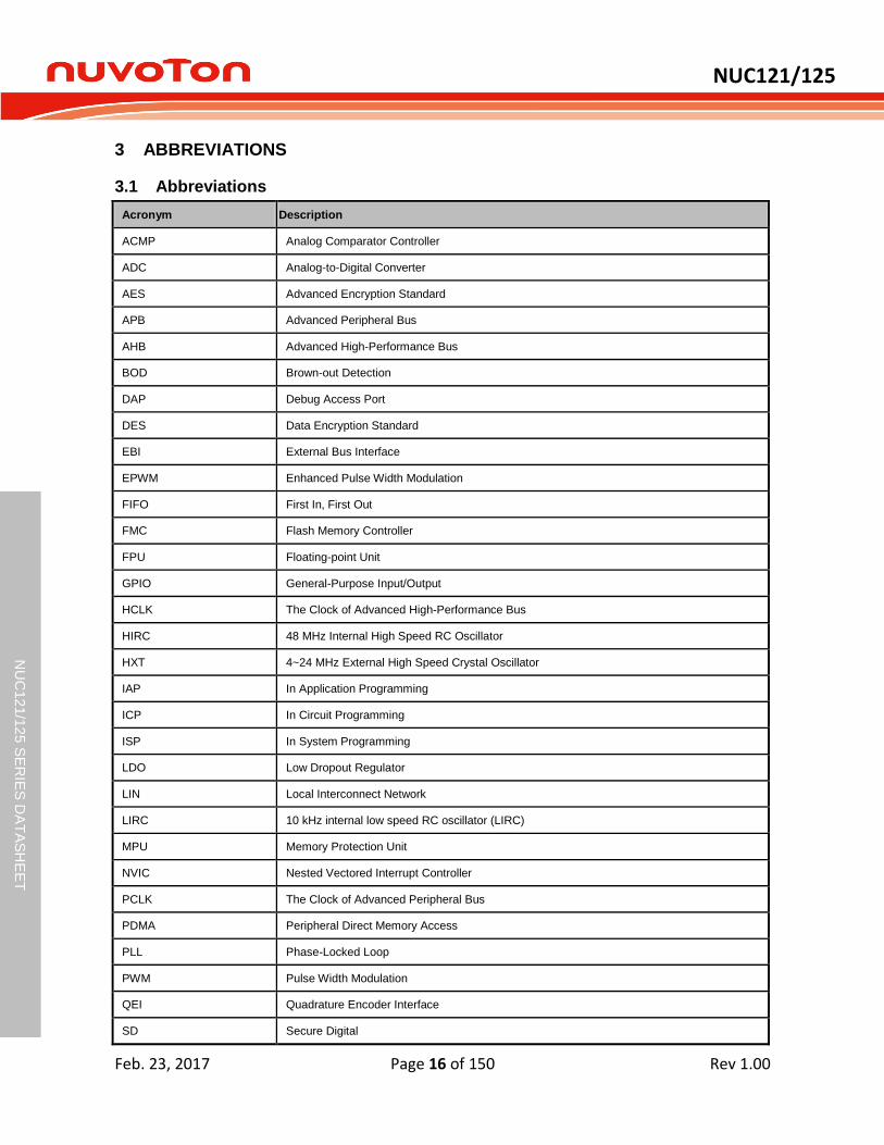
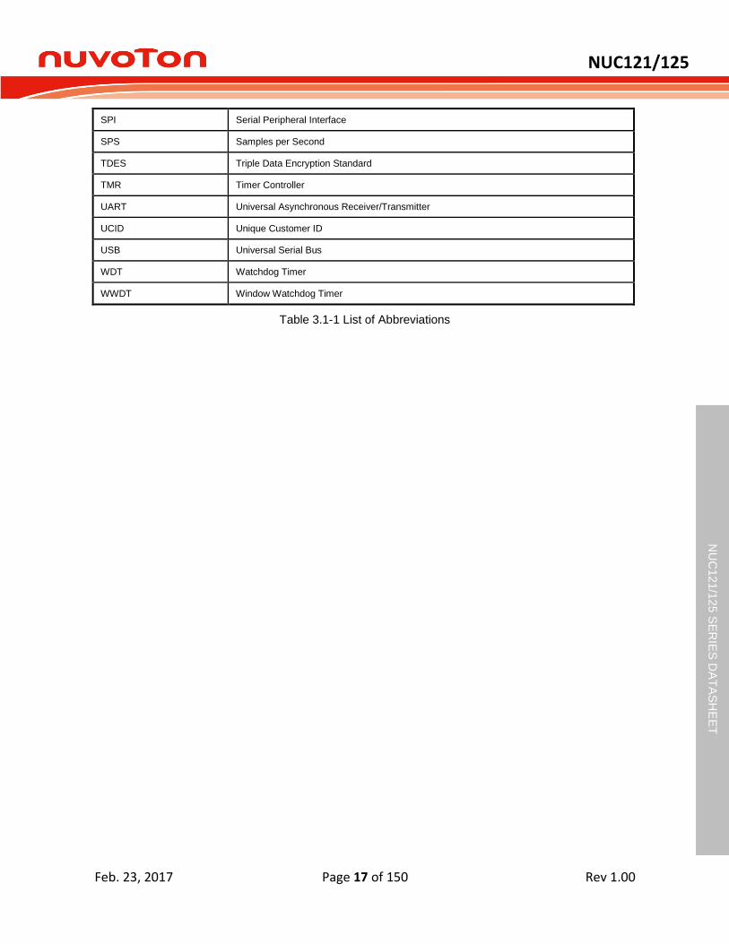
3 ABBREVIATIONS
Abbreviations 3.1
Acronym Description
ACMP Analog Comparator Controller
ADC Analog-to-Digital Converter
AES Advanced Encryption Standard
APB Advanced Peripheral Bus
AHB Advanced High-Performance Bus
BOD Brown-out Detection
DAP Debug Access Port
DES Data Encryption Standard
EBI External Bus Interface
EPWM Enhanced Pulse Width Modulation
FIFO First In, First Out
FMC Flash Memory Controller
FPU Floating-point Unit
GPIO General-Purpose Input/Output
HCLK The Clock of Advanced High-Performance Bus
HIRC 48 MHz Internal High Speed RC Oscillator
HXT 4~24 MHz External High Speed Crystal Oscillator
IAP In Application Programming
ICP In Circuit Programming
ISP In System Programming
LDO Low Dropout Regulator
LIN Local Interconnect Network
LIRC 10 kHz internal low speed RC oscillator (LIRC)
MPU Memory Protection Unit
NVIC Nested Vectored Interrupt Controller
PCLK The Clock of Advanced Peripheral Bus
PDMA Peripheral Direct Memory Access
PLL Phase-Locked Loop
PWM Pulse Width Modulation
QEI Quadrature Encoder Interface
SD Secure Digital
NUC121/125
Feb. 23, 2017 Page 17 of 150 Rev 1.00
NU
C12
1/1
25 S
ER
IES
DA
TA
SH
EE
T
SPI Serial Peripheral Interface
SPS Samples per Second
TDES Triple Data Encryption Standard
TMR Timer Controller
UART Universal Asynchronous Receiver/Transmitter
UCID Unique Customer ID
USB Universal Serial Bus
WDT Watchdog Timer
WWDT Window Watchdog Timer
Table 3.1-1 List of Abbreviations
NUC121/125
Feb. 23, 2017 Page 18 of 150 Rev 1.00
NU
C12
1/1
25 S
ER
IES
DA
TA
SH
EE
T
4 PARTS INFORMATION LIST AND PIN CONFIGURATION
NuMicro® NUC121/125 Selection Guide 4.1
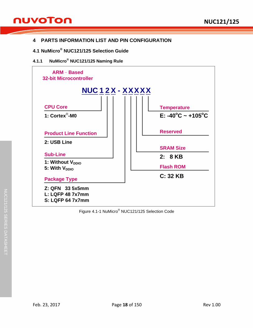
4.1.1 NuMicro® NUC121/125 Naming Rule
NUC
ARM–Based
32-bit Microcontroller
CPU Core
1: Cortex®-M0
Product Line Function
1 2 X - XXXXX
2: USB Line
Sub-Line
Package Type
Z: QFN 33 5x5mm
L: LQFP 48 7x7mm
S: LQFP 64 7x7mm
Temperature
E: -40oC ~ +105
oC
Reserved
SRAM Size
2: 8 KB
Flash ROM
C: 32 KB
1: Without VDDIO
5: With VDDIO
Figure 4.1-1 NuMicro® NUC121/125 Selection Code
NUC121/125
Feb. 23, 2017 Page 19 of 150 Rev 1.00
NU
C12
1/1
25 S
ER
IES
DA
TA
SH
EE
T
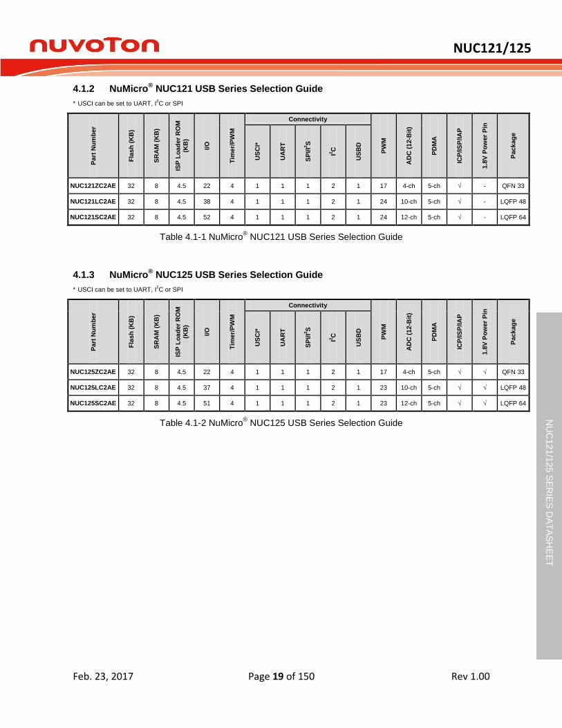
4.1.2 NuMicro® NUC121 USB Series Selection Guide
* USCI can be set to UART, I2C or SPI
Part
Nu
mb
er
Fla
sh
(K
B)
SR
AM
(K
B)
ISP
Lo
ad
er
RO
M
(KB
)
I/O
Tim
er/
PW
M
Connectivity
PW
M
AD
C (
12-B
it)
PD
MA
ICP
/IS
P/IA
P
1.8
V P
ow
er
Pin
Pack
ag
e
US
CI*
UA
RT
SP
I/I2
S
I2C
US
BD
NUC121ZC2AE 32 8 4.5 22 4 1 1 1 2 1 17 4-ch 5-ch √ - QFN 33
NUC121LC2AE 32 8 4.5 38 4 1 1 1 2 1 24 10-ch 5-ch √ - LQFP 48
NUC121SC2AE 32 8 4.5 52 4 1 1 1 2 1 24 12-ch 5-ch √ - LQFP 64
Table 4.1-1 NuMicro® NUC121 USB Series Selection Guide
4.1.3 NuMicro® NUC125 USB Series Selection Guide
* USCI can be set to UART, I2C or SPI
Part
Nu
mb
er
Fla
sh
(K
B)
SR
AM
(K
B)
ISP
Lo
ad
er
RO
M
(KB
)
I/O
Tim
er/
PW
M
Connectivity
PW
M
AD
C (
12-B
it)
PD
MA
ICP
/IS
P/IA
P
1.8
V P
ow
er
Pin
Pack
ag
e
US
CI*
UA
RT
SP
I/I2
S
I2C
US
BD
NUC125ZC2AE 32 8 4.5 22 4 1 1 1 2 1 17 4-ch 5-ch √ √ QFN 33
NUC125LC2AE 32 8 4.5 37 4 1 1 1 2 1 23 10-ch 5-ch √ √ LQFP 48
NUC125SC2AE 32 8 4.5 51 4 1 1 1 2 1 23 12-ch 5-ch √ √ LQFP 64
Table 4.1-2 NuMicro® NUC125 USB Series Selection Guide
NUC121/125
Feb. 23, 2017 Page 20 of 150 Rev 1.00
NU
C12
1/1
25 S
ER
IES
DA
TA
SH
EE
T
Pin Configuration 4.2
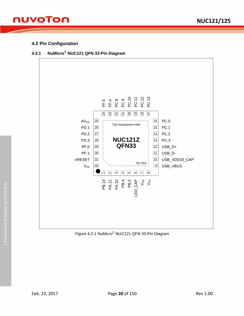
4.2.1 NuMicro® NUC121 QFN 33-Pin Diagram
NUC121ZQFN33
33 VSS
1 2 3 4 5 6 7 8
16
15
14
13
12
11
10
9
24
23
22
21
20
19
18
17
25
26
27
28
29
30
31
32
AVDD
PD.1
PD.2
PD.3
PF.0
PF.1
nRESET
VSS
PB
.14
PA
.11
PA
.10
PB
.4
PB
.5
LD
O_
CA
P
VD
D
VS
S
PC.0
PC.1
PC.2
PC.3
USB_D+
USB_D-
USB_VDD33_CAP
USB_VBUS
PF
.5
PF
.4
PC
.8
PC
.9
PC
.10
PC
.11
PC
.12
PC
.13
Top transparent view
Figure 4.2-1 NuMicro® NUC121 QFN 33-Pin Diagram
NUC121/125
Feb. 23, 2017 Page 21 of 150 Rev 1.00
NU
C12
1/1
25 S
ER
IES
DA
TA
SH
EE
T
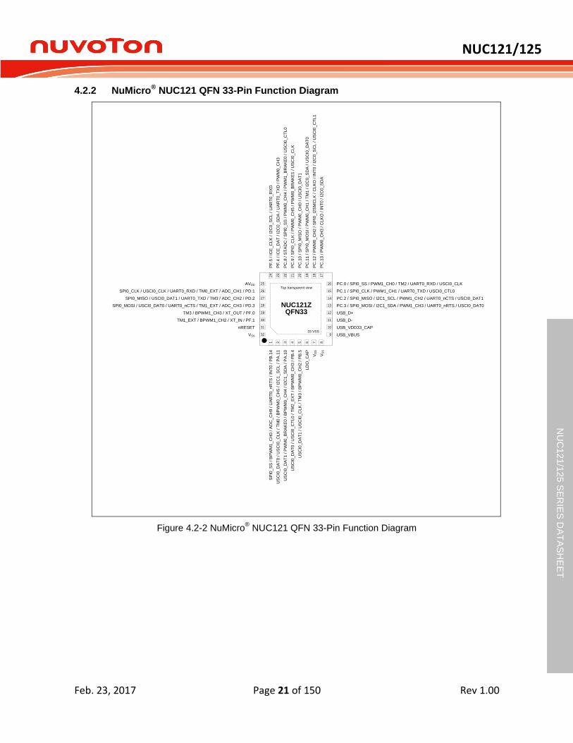
4.2.2 NuMicro® NUC121 QFN 33-Pin Function Diagram
NUC121ZQFN33
33 VSS
1 2 3 4 5 6 7 8
16
15
14
13
12
11
10
9
24
23
22
21
20
19
18
17
25
26
27
28
29
30
31
32
AVDD
SPI0_CLK / USCI0_CLK / UART0_RXD / TM0_EXT / ADC_CH1 / PD.1
SPI0_MISO / USCI0_DAT1 / UART0_TXD / TM3 / ADC_CH2 / PD.2
SPI0_MOSI / USCI0_DAT0 / UART0_nCTS / TM1_EXT / ADC_CH3 / PD.3
TM3 / BPWM1_CH3 / XT_OUT / PF.0
TM1_EXT / BPWM1_CH2 / XT_IN / PF.1
nRESET
VSS
SP
I0_
SS
/ B
PW
M1
_C
H0
/ A
DC
_C
H9
/ U
AR
T0
_n
RT
S / I
NT
0 / P
B.1
4
US
CI0
_D
AT
0 / U
SC
I0_
CL
K / T
M0
/ B
PW
M0
_C
H5
/ I
2C
1_
SC
L /
PA
.11
US
CI0
_D
AT
1 / P
WM
0_
BR
AK
E0
/ B
PW
M0
_C
H4
/ I
2C
1_
SD
A / P
A.1
0
US
CI0
_D
AT
0 / U
SC
I0_
CT
L0
/ T
M2
_E
XT
/ B
PW
M0
_C
H3
/ P
B.4
US
CI0
_D
AT
1 / U
SC
I0_
CL
K /
TM
3 / B
PW
M0
_C
H2
/ P
B.5
LD
O_
CA
P
VD
D
VS
S
PC.0 / SPI0_SS / PWM1_CH0 / TM2 / UART0_RXD / USCI0_CLK
PC.1 / SPI0_CLK / PWM1_CH1 / UART0_TXD / USCI0_CTL0
PC.2 / SPI0_MISO / I2C1_SCL / PWM1_CH2 / UART0_nCTS / USCI0_DAT1
PC.3 / SPI0_MOSI / I2C1_SDA / PWM1_CH3 / UART0_nRTS / USCI0_DAT0
USB_D+
USB_D-
USB_VDD33_CAP
USB_VBUS
PF
.5 / I
CE
_C
LK
/ I
2C
0_
SC
L / U
AR
T0
_R
XD
PF
.4 / I
CE
_D
AT
/ I
2C
0_
SD
A / U
AR
T0
_T
XD
/ P
WM
0_
CH
3
PC
.8 / S
TA
DC
/ S
PI0
_S
S /
PW
M0
_C
H4
/ P
WM
1_
BR
AK
E0
/ U
SC
I0_
CT
L0
PC
.9 / S
PI0
_C
LK
/ P
WM
0_
CH
5 / P
WM
0_
BR
AK
E1
/ U
SC
I0_
CL
K
PC
.10
/ S
PI0
_M
ISO
/ P
WM
0_
CH
0 / U
SC
I0_
DA
T1
PC
.11
/ S
PI0
_M
OS
I /
PW
M0
_C
H1
/ T
M1
/ I
2C
0_
SD
A / U
SC
I0_
DA
T0
PC
.12
/ P
WM
0_
CH
2 / S
PI0
_I2
SM
CL
K /
CL
KO
/ I
NT
0 / I2
C0
_S
CL
/ U
SC
I0_
CT
L1
PC
.13
/ P
WM
0_
CH
3 / C
LK
O /
IN
T0
/ I
2C
0_
SD
A
Top transparent view
Figure 4.2-2 NuMicro® NUC121 QFN 33-Pin Function Diagram
NUC121/125
Feb. 23, 2017 Page 22 of 150 Rev 1.00
NU
C12
1/1
25 S
ER
IES
DA
TA
SH
EE
T
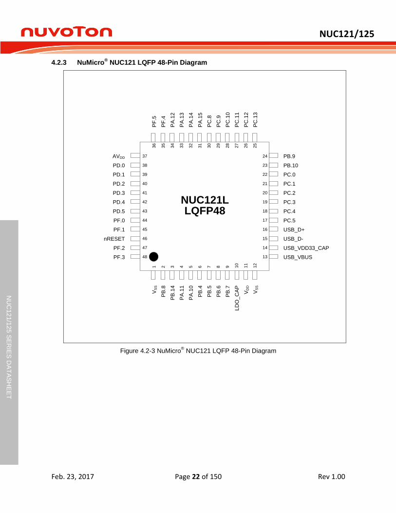
4.2.3 NuMicro® NUC121 LQFP 48-Pin Diagram
NUC121LLQFP48
1 2 3 4 5 6 7 8 9 10
11
12
24
23
22
21
20
19
18
17
16
15
14
13
36
35
34
33
32
31
30
29
28
27
26
25
37
38
39
40
41
42
43
44
45
46
47
48
VS
S
PB
.8
PB
.14
PA
.11
PA
.10
PB
.4
PB
.5
PB
.6
PB
.7
LD
O_
CA
P
VD
D
VS
S
PB.9
PB.10
PC.0
PC.1
PC.2
PC.3
PC.4
PC.5
USB_D+
USB_D-
USB_VDD33_CAP
USB_VBUS
PF
.5
PF
.4
PA
.12
PA
.13
PA
.14
PA
.15
PC
.8
PC
.9
PC
.10
PC
.11
PC
.12
PC
.13
AVDD
PD.0
PD.1
PD.2
PD.3
PD.4
PD.5
PF.0
PF.1
nRESET
PF.2
PF.3
Figure 4.2-3 NuMicro® NUC121 LQFP 48-Pin Diagram
NUC121/125
Feb. 23, 2017 Page 23 of 150 Rev 1.00
NU
C12
1/1
25 S
ER
IES
DA
TA
SH
EE
T
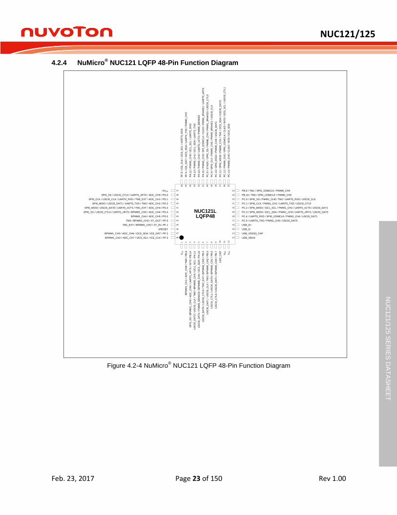
4.2.4 NuMicro® NUC121 LQFP 48-Pin Function Diagram
NUC121LLQFP48
1 2 3 4 5 6 7 8 9 10
11
12
24
23
22
21
20
19
18
17
16
15
14
13
36
35
34
33
32
31
30
29
28
27
26
25
37
38
39
40
41
42
43
44
45
46
47
48
VS
S
BP
WM
1_
CH
1 / A
DC
_C
H8
/ T
M0
/ P
B.8
SP
I0_
SS
/ B
PW
M1
_C
H0
/ A
DC
_C
H9
/ U
AR
T0
_n
RT
S / IN
T0
/ P
B.1
4
US
CI0
_D
AT
0 / U
SC
I0_C
LK
/ T
M0
/ B
PW
M0
_C
H5
/ I
2C
1_
SC
L /
PA
.11
US
CI0
_D
AT
1 / P
WM
0_
BR
AK
E0
/ B
PW
M0
_C
H4
/ I
2C
1_
SD
A / P
A.1
0
US
CI0
_D
AT
0 / U
SC
I0_
CT
L0
/ T
M2
_E
XT
/ B
PW
M0
_C
H3
/ P
B.4
US
CI0
_D
AT
1 / U
SC
I0_
CL
K /
TM
3 / B
PW
M0
_C
H2
/ P
B.5
US
CI0
_C
TL
1 / U
SC
I0_
DA
T0
/ B
PW
M0
_C
H1
/ P
B.6
US
CI0
_C
TL
0 / U
SC
I0_
DA
T1
/ B
PW
M0
_C
H0
/ P
B.7
LD
O_
CA
P
VD
D
VS
S
PB.9 / TM1 / SPI0_I2SMCLK / PWM0_CH4
PB.10 / TM2 / SPI0_I2SMCLK / PWM0_CH5
PC.0 / SPI0_SS / PWM1_CH0 / TM2 / UART0_RXD / USCI0_CLK
PC.1 / SPI0_CLK / PWM1_CH1 / UART0_TXD / USCI0_CTL0
PC.2 / SPI0_MISO / I2C1_SCL / PWM1_CH2 / UART0_nCTS / USCI0_DAT1
PC.3 / SPI0_MOSI / I2C1_SDA / PWM1_CH3 / UART0_nRTS / USCI0_DAT0
PC.4 / UART0_RXD / SPI0_I2SMCLK / PWM1_CH4 / USCI0_DAT1
PC.5 / UART0_TXD / PWM1_CH5 / USCI0_DAT0
USB_D+
USB_D-
USB_VDD33_CAP
USB_VBUS
PF
.5 / I
CE
_C
LK
/ I
2C
0_
SC
L /
UA
RT
0_
RX
D
PF
.4 / I
CE
_D
AT
/ I
2C
0_
SD
A / U
AR
T0
_T
XD
/ P
WM
0_
CH
3
PA
.12
/ P
WM
0_
CH
0 / I
2C
1_
SC
L /
UA
RT
0_
RX
D
PA
.13
/ P
WM
0_
CH
1 / I
2C
1_
SD
A / U
AR
T0
_T
XD
PA
.14
/ P
WM
0_
CH
2 / U
AR
T0
_n
CT
S / P
WM
0_
BR
AK
E0
PA
.15
/ P
WM
0_
CH
3 / S
PI_
I2S
MC
LK
/ C
LK
O /
PW
M1
_B
RA
KE
1 / U
AR
T0
_n
RT
S
PC
.8 / S
TA
DC
/ S
PI0
_S
S /
PW
M0
_C
H4
/ P
WM
1_
BR
AK
E0
/ U
SC
I0_
CT
L0
PC
.9 / S
PI0
_C
LK
/ P
WM
0_
CH
5 / P
WM
0_
BR
AK
E1
/ U
SC
I0_
CL
K
PC
.10
/ S
PI0
_M
ISO
/ P
WM
0_
CH
0 / U
SC
I0_
DA
T1
PC
.11
/ S
PI0
_M
OS
I /
PW
M0
_C
H1
/ T
M1
/ I
2C
0_
SD
A / U
SC
I0_
DA
T0
PC
.12
/ P
WM
0_
CH
2 / S
PI0
_I2
SM
CL
K / C
LK
O / I
NT
0 / I2
C0
_S
CL
/ U
SC
I0_
CT
L1
PC
.13
/ P
WM
0_
CH
3 / C
LK
O / I
NT
0 / I
2C
0_
SD
A
AVDD
SPI0_SS / USCI0_CTL0 / UART0_nRTS / ADC_CH0 / PD.0
SPI0_CLK / USCI0_CLK / UART0_RXD / TM0_EXT / ADC_CH1 / PD.1
SPI0_MISO / USCI0_DAT1 / UART0_TXD / TM3 / ADC_CH2 / PD.2
SPI0_MOSI / USCI0_DAT0 / UART0_nCTS / TM1_EXT / ADC_CH3 / PD.3
SPI0_SS / USCI0_CTL0 / UART0_nRTS / BPWM1_CH5 / ADC_CH4 / PD.4
BPWM1_CH4 / ADC_CH5 / PD.5
TM3 / BPWM1_CH3 / XT_OUT / PF.0
TM1_EXT / BPWM1_CH2 / XT_IN / PF.1
nRESET
BPWM1_CH3 / ADC_CH6 / I2C0_SDA / ICE_DAT / PF.2
BPWM1_CH2 / ADC_CH7 / I2C0_SCL / ICE_CLK / PF.3
Figure 4.2-4 NuMicro® NUC121 LQFP 48-Pin Function Diagram
NUC121/125
Feb. 23, 2017 Page 24 of 150 Rev 1.00
NU
C12
1/1
25 S
ER
IES
DA
TA
SH
EE
T
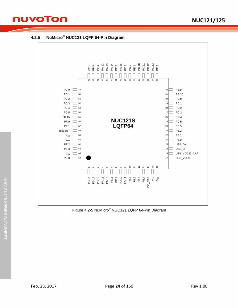
4.2.5 NuMicro® NUC121 LQFP 64-Pin Diagram
NUC121SLQFP64
1 2 3 4 5 6 7 8 9 10
11
12
13
14
15
16
32
31
30
29
28
27
26
25
24
23
22
21
20
19
18
17
48
47
46
45
44
43
42
41
40
39
38
37
36
35
34
33
49
50
51
52
53
54
55
56
57
58
59
60
61
62
63
64
PB
.14
PB
.13
PB
.12
PA
.11
PA
.10
PD
.8
PD
.9
PD
.10
PD
.11
PB
.4
PB
.5
PB
.6
PB
.7
LD
O_
CA
P
VD
D
VS
S
PB.9
PB.10
PC.0
PC.1
PC.2
PC.3
PC.4
PC.5
PB.3
PB.2
PB.1
PB.0
USB_D+
USB_D-
USB_VDD33_CAP
USB_VBUS
AV
DD
PF
.5
PF
.4
PA
.12
PA
.13
PA
.14
PE
.0
PA
.15
PC
.8
PC
.9
PE
.1
PC
.10
PC
.11
PC
.12
PC
.13
PE
.2
PD.0
PD.1
PD.2
PD.3
PD.4
PD.5
PB.15
PF.0
PF.1
nRESET
VSS
VDD
PF.2
PF.3
VSS
PB.8
Figure 4.2-5 NuMicro® NUC121 LQFP 64-Pin Diagram
NUC121/125
Feb. 23, 2017 Page 25 of 150 Rev 1.00
NU
C12
1/1
25 S
ER
IES
DA
TA
SH
EE
T
4.2.6 NuMicro® NUC121 LQFP 64-Pin Function Diagram
NUC121SLQFP64
1 2 3 4 5 6 7 8 9 10
11
12
13
14
15
16
32
31
30
29
28
27
26
25
24
23
22
21
20
19
18
17
48
47
46
45
44
43
42
41
40
39
38
37
36
35
34
33
49
50
51
52
53
54
55
56
57
58
59
60
61
62
63
64
SP
I0_
SS
/ B
PW
M1
_C
H0
/ A
DC
_C
H9
/ U
AR
T0
_n
RT
S / I
NT
0 / P
B.1
4
US
CI0
_C
TL
1 / A
DC
_C
H1
0 / P
B.1
3
US
CI0
_C
TL
0 / A
DC
_C
H1
1 / C
LK
O /
PB
.12
US
CI0
_D
AT
0 / U
SC
I0_C
LK
/ T
M0
/ B
PW
M0
_C
H5
/ I
2C
1_
SC
L /
PA
.11
US
CI0
_D
AT
1 / P
WM
0_
BR
AK
E0
/ B
PW
M0
_C
H4
/ I2
C1
_S
DA
/ P
A.1
0
US
CI0
_D
AT
0 / P
D.8
PW
M0
_B
RA
KE
1 / P
D.9
BP
WM
0_
CH
5 / C
LK
O / P
D.1
0
BP
WM
0_
CH
4 / I
NT
1 / P
D.1
1
US
CI0
_D
AT
0 / U
SC
I0_
CT
L0
/ T
M2
_E
XT
/ B
PW
M0
_C
H3
/ P
B.4
US
CI0
_D
AT
1 / U
SC
I0_
CL
K /
TM
3 / B
PW
M0
_C
H2
/ P
B.5
US
CI0
_C
TL
1 / U
SC
I0_
DA
T0
/ B
PW
M0
_C
H1
/ P
B.6
US
CI0
_C
TL
0 / U
SC
I0_
DA
T1
/ B
PW
M0
_C
H0
/ P
B.7
LD
O_
CA
P
VD
D
VS
S
PB.9 / TM1 / SPI0_I2SMCLK / PWM0_CH4
PB.10 / TM2 / SPI0_I2SMCLK / PWM0_CH5
PC.0 / SPI0_SS / PWM1_CH0 / TM2 / UART0_RXD / USCI0_CLK
PC.1 / SPI0_CLK / PWM1_CH1 / UART0_TXD / USCI0_CTL0
PC.2 / SPI0_MISO / I2C1_SCL / PWM1_CH2 / UART0_nCTS / USCI0_DAT1
PC.3 / SPI0_MOSI / I2C1_SDA / PWM1_CH3 / UART0_nRTS / USCI0_DAT0
PC.4 / UART0_RXD / SPI0_I2SMCLK / PWM1_CH4 / USCI0_DAT1
PC.5 / UART0_TXD / PWM1_CH5 / USCI0_DAT0
PB.3 / UART0_nCTS / TM3_EXT / PWM1_CH3
PB.2 / UART0_nRTS / TM2_EXT / PWM1_CH2
PB.1 / UART0_TXD / PWM1_CH1
PB.0 / UART0_RXD / PWM1_CH0
USB_D+
USB_D-
USB_VDD33_CAP
USB_VBUS
AV
DD
PF
.5 / I
CE
_C
LK
/ I
2C
0_
SC
L /
UA
RT
0_
RX
D
PF
.4 / I
CE
_D
AT
/ I2
C0
_S
DA
/ U
AR
T0
_T
XD
/ P
WM
0_
CH
3
PA
.12
/ P
WM
0_
CH
0 / I
2C
1_
SC
L /
UA
RT
0_
RX
D
PA
.13
/ P
WM
0_
CH
1 / I
2C
1_
SD
A / U
AR
T0
_T
XD
PA
.14
/ P
WM
0_
CH
2 / U
AR
T0
_n
CT
S / P
WM
0_
BR
AK
E0
PE
.0 / I
NT
0 / C
LK
O /
PW
M0
_C
H3
/ T
M1
_E
XT
/ U
SC
I0_
DA
T0
PA
.15
/ P
WM
0_
CH
3 / S
PI_
I2S
MC
LK
/ C
LK
O / P
WM
1_
BR
AK
E1
/ U
AR
T0
_n
RT
S
PC
.8 / S
TA
DC
/ S
PI0
_S
S / P
WM
0_
CH
4 / P
WM
1_
BR
AK
E0
/ U
SC
I0_
CT
L0
PC
.9 / S
PI0
_C
LK
/ P
WM
0_
CH
5 / P
WM
0_
BR
AK
E1
/ U
SC
I0_
CL
K
PE
.1 / S
TA
DC
/ C
LK
O / T
M3
/ U
SC
I0_
DA
T1
PC
.10
/ S
PI0
_M
ISO
/ P
WM
0_
CH
0 / U
SC
I0_
DA
T1
PC
.11
/ S
PI0
_M
OS
I / P
WM
0_
CH
1 / T
M1
/ I
2C
0_
SD
A / U
SC
I0_
DA
T0
PC
.12
/ P
WM
0_
CH
2 / S
PI0
_I2
SM
CL
K / C
LK
O /
IN
T0
/ I
2C
0_
SC
L / U
SC
I0_
CT
L1
PC
.13
/ P
WM
0_
CH
3 / C
LK
O / I
NT
0 / I2
C0
_S
DA
PE
.2 / I
NT
1 / T
M0
_E
XT
/ I
2C
0_
SC
L / U
SC
I0_
CT
L1
SPI0_SS / USCI0_CTL0 / UART0_nRTS / ADC_CH0 / PD.0
SPI0_CLK / USCI0_CLK / UART0_RXD / TM0_EXT / ADC_CH1 / PD.1
SPI0_MISO / USCI0_DAT1 / UART0_TXD / TM3 / ADC_CH2 / PD.2
SPI0_MOSI / USCI0_DAT0 / UART0_nCTS / TM1_EXT / ADC_CH3 / PD.3
SPI0_SS / USCI0_CTL0 / UART0_nRTS / BPWM1_CH5 / ADC_CH4 / PD.4
BPWM1_CH4 / ADC_CH5 / PD.5
BPWM1_CH5 / TM0_EXT / INT1 / PB.15
TM3 / BPWM1_CH3 / XT_OUT / PF.0
TM1_EXT / BPWM1_CH2 / XT_IN / PF.1
nRESET
VSS
VDD
BPWM1_CH3 / ADC_CH6 / I2C0_SDA / ICE_DAT / PF.2
BPWM1_CH2 / ADC_CH7 / I2C0_SCL / ICE_CLK / PF.3
VSS
BPWM1_CH1 / ADC_CH8 / TM0 / PB.8
Figure 4.2-6 NuMicro® NUC121 LQFP 64-Pin Function Diagram
NUC121/125
Feb. 23, 2017 Page 26 of 150 Rev 1.00
NU
C12
1/1
25 S
ER
IES
DA
TA
SH
EE
T
4.2.7 NuMicro® NUC125 QFN 33-Pin Diagram
NUC125ZQFN33
33 VSS
1 2 3 4 5 6 7 8
16
15
14
13
12
11
10
9
24
23
22
21
20
19
18
17
25
26
27
28
29
30
31
32
AVDD
PD.1
PD.2
PD.3
PF.0
PF.1
nRESET
VDDIO
PB
.14
PA
.11
PA
.10
PB
.4
PB
.5
LD
O_C
AP
VD
D
VS
S
PC.0
PC.1
PC.2
PC.3
USB_D+
USB_D-
USB_VDD33_CAP
USB_VBUS
PF
.5
PF
.4
PC
.8
PC
.9
PC
.10
PC
.11
PC
.12
PC
.13
Top transparent view
VDDIO power domain
Figure 4.2-7 NuMicro® NUC125 QFN 33-Pin Diagram
NUC121/125
Feb. 23, 2017 Page 27 of 150 Rev 1.00
NU
C12
1/1
25 S
ER
IES
DA
TA
SH
EE
T
4.2.8 NuMicro® NUC125 QFN 33-Pin Function Diagram
NUC125ZQFN33
33 VSS
1 2 3 4 5 6 7 8
16
15
14
13
12
11
10
9
24
23
22
21
20
19
18
17
25
26
27
28
29
30
31
32
AVDD
SPI0_CLK / USCI0_CLK / UART0_RXD / TM0_EXT / ADC_CH1 / PD.1
SPI0_MISO / USCI0_DAT1 / UART0_TXD / TM3 / ADC_CH2 / PD.2
SPI0_MOSI / USCI0_DAT0 / UART0_nCTS / TM1_EXT / ADC_CH3 / PD.3
TM3 / BPWM1_CH3 / XT_OUT / PF.0
TM1_EXT / BPWM1_CH2 / XT_IN / PF.1
nRESET
VDDIO
SP
I0_
SS
/ B
PW
M1
_C
H0
/ A
DC
_C
H9
/ U
AR
T0
_n
RT
S / I
NT
0 / P
B.1
4
US
CI0
_D
AT
0 / U
SC
I0_
CL
K / T
M0
/ B
PW
M0
_C
H5
/ I
2C
1_
SC
L /
PA
.11
US
CI0
_D
AT
1 / P
WM
0_
BR
AK
E0
/ B
PW
M0
_C
H4
/ I
2C
1_
SD
A / P
A.1
0
US
CI0
_D
AT
0 / U
SC
I0_
CT
L0
/ T
M2
_E
XT
/ B
PW
M0
_C
H3
/ P
B.4
US
CI0
_D
AT
1 / U
SC
I0_
CL
K /
TM
3 / B
PW
M0
_C
H2
/ P
B.5
LD
O_
CA
P
VD
D
VS
S
PC.0 / SPI0_SS / PWM1_CH0 / TM2 / UART0_RXD / USCI0_CLK
PC.1 / SPI0_CLK / PWM1_CH1 / UART0_TXD / USCI0_CTL0
PC.2 / SPI0_MISO / I2C1_SCL / PWM1_CH2 / UART0_nCTS / USCI0_DAT1
PC.3 / SPI0_MOSI / I2C1_SDA / PWM1_CH3 / UART0_nRTS / USCI0_DAT0
USB_D+
USB_D-
USB_VDD33_CAP
USB_VBUS
PF
.5 / I
CE
_C
LK
/ I
2C
0_
SC
L / U
AR
T0
_R
XD
PF
.4 / I
CE
_D
AT
/ I
2C
0_
SD
A / U
AR
T0
_T
XD
/ P
WM
0_
CH
3
PC
.8 / S
TA
DC
/ S
PI0
_S
S /
PW
M0
_C
H4
/ P
WM
1_
BR
AK
E0
/ U
SC
I0_
CT
L0
PC
.9 / S
PI0
_C
LK
/ P
WM
0_
CH
5 / P
WM
0_
BR
AK
E1
/ U
SC
I0_
CL
K
PC
.10
/ S
PI0
_M
ISO
/ P
WM
0_
CH
0 / U
SC
I0_
DA
T1
PC
.11
/ S
PI0
_M
OS
I /
PW
M0
_C
H1
/ T
M1
/ I
2C
0_
SD
A / U
SC
I0_
DA
T0
PC
.12
/ P
WM
0_
CH
2 / S
PI0
_I2
SM
CL
K /
CL
KO
/ I
NT
0 / I2
C0
_S
CL
/ U
SC
I0_
CT
L1
PC
.13
/ P
WM
0_
CH
3 / C
LK
O /
IN
T0
/ I
2C
0_
SD
A
Top transparent view
VDDIO power domain
Figure 4.2-8 NuMicro® NUC125 QFN 33-Pin Function Diagram
NUC121/125
Feb. 23, 2017 Page 28 of 150 Rev 1.00
NU
C12
1/1
25 S
ER
IES
DA
TA
SH
EE
T
4.2.9 NuMicro® NUC125 LQFP 48-Pin Diagram
NUC125LLQFP48
1 2 3 4 5 6 7 8 9 10
11
12
24
23
22
21
20
19
18
17
16
15
14
13
36
35
34
33
32
31
30
29
28
27
26
25
37
38
39
40
41
42
43
44
45
46
47
48
VS
S
VD
DIO
PB
.14
PA
.11
PA
.10
PB
.4
PB
.5
PB
.6
PB
.7
LD
O_C
AP
VD
D
VS
S
PB.9
PB.10
PC.0
PC.1
PC.2
PC.3
PC.4
PC.5
USB_D+
USB_D-
USB_VDD33_CAP
USB_VBUS
PF
.5
PF
.4
PA
.12
PA
.13
PA
.14
PA
.15
PC
.8
PC
.9
PC
.10
PC
.11
PC
.12
PC
.13
AVDD
PD.0
PD.1
PD.2
PD.3
PD.4
PD.5
PF.0
PF.1
nRESET
PF.2
PF.3
VDDIO power domain
Figure 4.2-9 NuMicro® NUC125 LQFP 48-Pin Diagram
NUC121/125
Feb. 23, 2017 Page 29 of 150 Rev 1.00
NU
C12
1/1
25 S
ER
IES
DA
TA
SH
EE
T
4.2.10 NuMicro® NUC125 LQFP 48-Pin Function Diagram
NUC125LLQFP48
1 2 3 4 5 6 7 8 9 10
11
12
24
23
22
21
20
19
18
17
16
15
14
13
36
35
34
33
32
31
30
29
28
27
26
25
37
38
39
40
41
42
43
44
45
46
47
48
VS
S
VD
DIO
SP
I0_
SS
/ B
PW
M1
_C
H0
/ A
DC
_C
H9
/ U
AR
T0
_n
RT
S / IN
T0
/ P
B.1
4
US
CI0
_D
AT
0 / U
SC
I0_C
LK
/ T
M0
/ B
PW
M0
_C
H5
/ I
2C
1_
SC
L /
PA
.11
US
CI0
_D
AT
1 / P
WM
0_
BR
AK
E0
/ B
PW
M0
_C
H4
/ I
2C
1_
SD
A / P
A.1
0
US
CI0
_D
AT
0 / U
SC
I0_
CT
L0
/ T
M2
_E
XT
/ B
PW
M0
_C
H3
/ P
B.4
US
CI0
_D
AT
1 / U
SC
I0_
CL
K /
TM
3 / B
PW
M0
_C
H2
/ P
B.5
US
CI0
_C
TL
1 / U
SC
I0_
DA
T0
/ B
PW
M0
_C
H1
/ P
B.6
US
CI0
_C
TL
0 / U
SC
I0_
DA
T1
/ B
PW
M0
_C
H0
/ P
B.7
LD
O_
CA
P
VD
D
VS
S
PB.9 / TM1 / SPI0_I2SMCLK / PWM0_CH4
PB.10 / TM2 / SPI0_I2SMCLK / PWM0_CH5
PC.0 / SPI0_SS / PWM1_CH0 / TM2 / UART0_RXD / USCI0_CLK
PC.1 / SPI0_CLK / PWM1_CH1 / UART0_TXD / USCI0_CTL0
PC.2 / SPI0_MISO / I2C1_SCL / PWM1_CH2 / UART0_nCTS / USCI0_DAT1
PC.3 / SPI0_MOSI / I2C1_SDA / PWM1_CH3 / UART0_nRTS / USCI0_DAT0
PC.4 / UART0_RXD / SPI0_I2SMCLK / PWM1_CH4 / USCI0_DAT1
PC.5 / UART0_TXD / PWM1_CH5 / USCI0_DAT0
USB_D+
USB_D-
USB_VDD33_CAP
USB_VBUS
PF
.5 / I
CE
_C
LK
/ I
2C
0_
SC
L /
UA
RT
0_
RX
D
PF
.4 / I
CE
_D
AT
/ I
2C
0_
SD
A / U
AR
T0
_T
XD
/ P
WM
0_
CH
3
PA
.12
/ P
WM
0_
CH
0 / I
2C
1_
SC
L /
UA
RT
0_
RX
D
PA
.13
/ P
WM
0_
CH
1 / I
2C
1_
SD
A / U
AR
T0
_T
XD
PA
.14
/ P
WM
0_
CH
2 / U
AR
T0
_n
CT
S / P
WM
0_
BR
AK
E0
PA
.15
/ P
WM
0_
CH
3 / S
PI_
I2S
MC
LK
/ C
LK
O /
PW
M1
_B
RA
KE
1 / U
AR
T0
_n
RT
S
PC
.8 / S
TA
DC
/ S
PI0
_S
S /
PW
M0
_C
H4
/ P
WM
1_
BR
AK
E0
/ U
SC
I0_
CT
L0
PC
.9 / S
PI0
_C
LK
/ P
WM
0_
CH
5 / P
WM
0_
BR
AK
E1
/ U
SC
I0_
CL
K
PC
.10
/ S
PI0
_M
ISO
/ P
WM
0_
CH
0 / U
SC
I0_
DA
T1
PC
.11
/ S
PI0
_M
OS
I /
PW
M0
_C
H1
/ T
M1
/ I
2C
0_
SD
A / U
SC
I0_
DA
T0
PC
.12
/ P
WM
0_
CH
2 / S
PI0
_I2
SM
CL
K / C
LK
O / I
NT
0 / I2
C0
_S
CL
/ U
SC
I0_
CT
L1
PC
.13
/ P
WM
0_
CH
3 / C
LK
O / I
NT
0 / I
2C
0_
SD
A
AVDD
SPI0_SS / USCI0_CTL0 / UART0_nRTS / ADC_CH0 / PD.0
SPI0_CLK / USCI0_CLK / UART0_RXD / TM0_EXT / ADC_CH1 / PD.1
SPI0_MISO / USCI0_DAT1 / UART0_TXD / TM3 / ADC_CH2 / PD.2
SPI0_MOSI / USCI0_DAT0 / UART0_nCTS / TM1_EXT / ADC_CH3 / PD.3
SPI0_SS / USCI0_CTL0 / UART0_nRTS / BPWM1_CH5 / ADC_CH4 / PD.4
BPWM1_CH4 / ADC_CH5 / PD.5
TM3 / BPWM1_CH3 / XT_OUT / PF.0
TM1_EXT / BPWM1_CH2 / XT_IN / PF.1
nRESET
BPWM1_CH3 / ADC_CH6 / I2C0_SDA / ICE_DAT / PF.2
BPWM1_CH2 / ADC_CH7 / I2C0_SCL / ICE_CLK / PF.3
VDDIO power domain
Figure 4.2-10 NuMicro® NUC125 LQFP 48-Pin Function Diagram
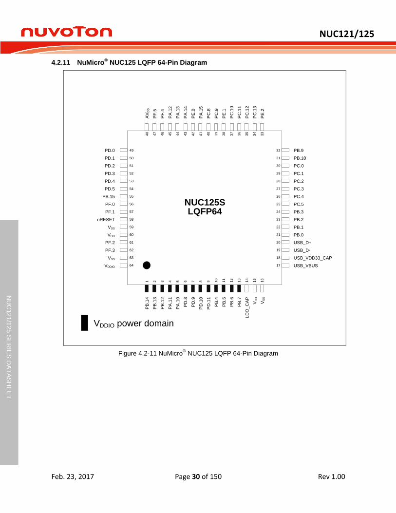
NUC121/125
Feb. 23, 2017 Page 30 of 150 Rev 1.00
NU
C12
1/1
25 S
ER
IES
DA
TA
SH
EE
T
4.2.11 NuMicro® NUC125 LQFP 64-Pin Diagram
NUC125SLQFP64
1 2 3 4 5 6 7 8 9 10
11
12
13
14
15
16
32
31
30
29
28
27
26
25
24
23
22
21
20
19
18
17
48
47
46
45
44
43
42
41
40
39
38
37
36
35
34
33
49
50
51
52
53
54
55
56
57
58
59
60
61
62
63
64
PB
.14
PB
.13
PB
.12
PA
.11
PA
.10
PD
.8
PD
.9
PD
.10
PD
.11
PB
.4
PB
.5
PB
.6
PB
.7
LD
O_
CA
P
VD
D
VS
S
PB.9
PB.10
PC.0
PC.1
PC.2
PC.3
PC.4
PC.5
PB.3
PB.2
PB.1
PB.0
USB_D+
USB_D-
USB_VDD33_CAP
USB_VBUS
AV
DD
PF
.5
PF
.4
PA
.12
PA
.13
PA
.14
PE
.0
PA
.15
PC
.8
PC
.9
PE
.1
PC
.10
PC
.11
PC
.12
PC
.13
PE
.2
PD.0
PD.1
PD.2
PD.3
PD.4
PD.5
PB.15
PF.0
PF.1
nRESET
VSS
VDD
PF.2
PF.3
VSS
VDDIO
VDDIO power domain
Figure 4.2-11 NuMicro® NUC125 LQFP 64-Pin Diagram
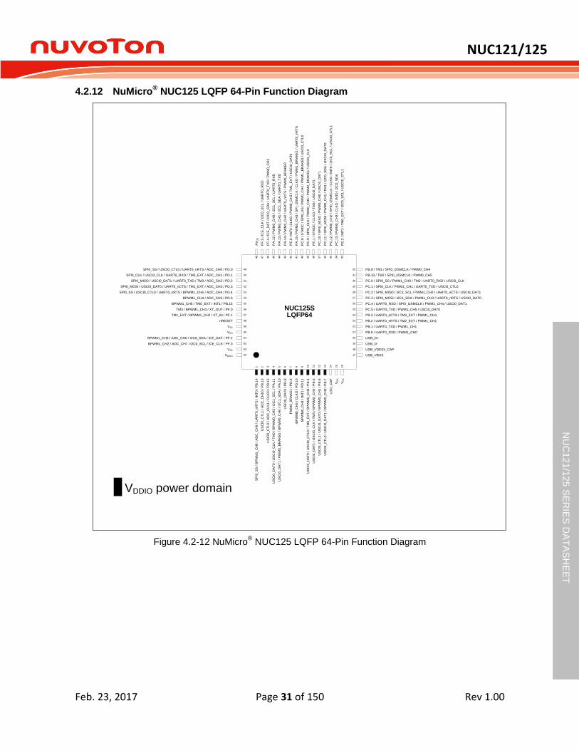
NUC121/125
Feb. 23, 2017 Page 31 of 150 Rev 1.00
NU
C12
1/1
25 S
ER
IES
DA
TA
SH
EE
T
4.2.12 NuMicro® NUC125 LQFP 64-Pin Function Diagram
NUC125SLQFP64
1 2 3 4 5 6 7 8 9 10
11
12
13
14
15
16
32
31
30
29
28
27
26
25
24
23
22
21
20
19
18
17
48
47
46
45
44
43
42
41
40
39
38
37
36
35
34
33
49
50
51
52
53
54
55
56
57
58
59
60
61
62
63
64
SP
I0_
SS
/ B
PW
M1
_C
H0
/ A
DC
_C
H9
/ U
AR
T0
_n
RT
S / I
NT
0 / P
B.1
4
US
CI0
_C
TL
1 / A
DC
_C
H1
0 / P
B.1
3
US
CI0
_C
TL
0 / A
DC
_C
H1
1 / C
LK
O /
PB
.12
US
CI0
_D
AT
0 / U
SC
I0_C
LK
/ T
M0
/ B
PW
M0
_C
H5
/ I
2C
1_
SC
L /
PA
.11
US
CI0
_D
AT
1 / P
WM
0_
BR
AK
E0
/ B
PW
M0
_C
H4
/ I2
C1
_S
DA
/ P
A.1
0
US
CI0
_D
AT
0 / P
D.8
PW
M0
_B
RA
KE
1 / P
D.9
BP
WM
0_
CH
5 / C
LK
O / P
D.1
0
BP
WM
0_
CH
4 / I
NT
1 / P
D.1
1
US
CI0
_D
AT
0 / U
SC
I0_
CT
L0
/ T
M2
_E
XT
/ B
PW
M0
_C
H3
/ P
B.4
US
CI0
_D
AT
1 / U
SC
I0_
CL
K /
TM
3 / B
PW
M0
_C
H2
/ P
B.5
US
CI0
_C
TL
1 / U
SC
I0_
DA
T0
/ B
PW
M0
_C
H1
/ P
B.6
US
CI0
_C
TL
0 / U
SC
I0_
DA
T1
/ B
PW
M0
_C
H0
/ P
B.7
LD
O_
CA
P
VD
D
VS
S
PB.9 / TM1 / SPI0_I2SMCLK / PWM0_CH4
PB.10 / TM2 / SPI0_I2SMCLK / PWM0_CH5
PC.0 / SPI0_SS / PWM1_CH0 / TM2 / UART0_RXD / USCI0_CLK
PC.1 / SPI0_CLK / PWM1_CH1 / UART0_TXD / USCI0_CTL0
PC.2 / SPI0_MISO / I2C1_SCL / PWM1_CH2 / UART0_nCTS / USCI0_DAT1
PC.3 / SPI0_MOSI / I2C1_SDA / PWM1_CH3 / UART0_nRTS / USCI0_DAT0
PC.4 / UART0_RXD / SPI0_I2SMCLK / PWM1_CH4 / USCI0_DAT1
PC.5 / UART0_TXD / PWM1_CH5 / USCI0_DAT0
PB.3 / UART0_nCTS / TM3_EXT / PWM1_CH3
PB.2 / UART0_nRTS / TM2_EXT / PWM1_CH2
PB.1 / UART0_TXD / PWM1_CH1
PB.0 / UART0_RXD / PWM1_CH0
USB_D+
USB_D-
USB_VDD33_CAP
USB_VBUS
AV
DD
PF
.5 / I
CE
_C
LK
/ I
2C
0_
SC
L /
UA
RT
0_
RX
D
PF
.4 / I
CE
_D
AT
/ I2
C0
_S
DA
/ U
AR
T0
_T
XD
/ P
WM
0_
CH
3
PA
.12
/ P
WM
0_
CH
0 / I
2C
1_
SC
L /
UA
RT
0_
RX
D
PA
.13
/ P
WM
0_
CH
1 / I
2C
1_
SD
A / U
AR
T0
_T
XD
PA
.14
/ P
WM
0_
CH
2 / U
AR
T0
_n
CT
S / P
WM
0_
BR
AK
E0
PE
.0 / I
NT
0 / C
LK
O /
PW
M0
_C
H3
/ T
M1
_E
XT
/ U
SC
I0_
DA
T0
PA
.15
/ P
WM
0_
CH
3 / S
PI_
I2S
MC
LK
/ C
LK
O / P
WM
1_
BR
AK
E1
/ U
AR
T0
_n
RT
S
PC
.8 / S
TA
DC
/ S
PI0
_S
S / P
WM
0_
CH
4 / P
WM
1_
BR
AK
E0
/ U
SC
I0_
CT
L0
PC
.9 / S
PI0
_C
LK
/ P
WM
0_
CH
5 / P
WM
0_
BR
AK
E1
/ U
SC
I0_
CL
K
PE
.1 / S
TA
DC
/ C
LK
O / T
M3
/ U
SC
I0_
DA
T1
PC
.10
/ S
PI0
_M
ISO
/ P
WM
0_
CH
0 / U
SC
I0_
DA
T1
PC
.11
/ S
PI0
_M
OS
I / P
WM
0_
CH
1 / T
M1
/ I
2C
0_
SD
A / U
SC
I0_
DA
T0
PC
.12
/ P
WM
0_
CH
2 / S
PI0
_I2
SM
CL
K / C
LK
O /
IN
T0
/ I
2C
0_
SC
L / U
SC
I0_
CT
L1
PC
.13
/ P
WM
0_
CH
3 / C
LK
O / I
NT
0 / I2
C0
_S
DA
PE
.2 / I
NT
1 / T
M0
_E
XT
/ I
2C
0_
SC
L / U
SC
I0_
CT
L1
SPI0_SS / USCI0_CTL0 / UART0_nRTS / ADC_CH0 / PD.0
SPI0_CLK / USCI0_CLK / UART0_RXD / TM0_EXT / ADC_CH1 / PD.1
SPI0_MISO / USCI0_DAT1 / UART0_TXD / TM3 / ADC_CH2 / PD.2
SPI0_MOSI / USCI0_DAT0 / UART0_nCTS / TM1_EXT / ADC_CH3 / PD.3
SPI0_SS / USCI0_CTL0 / UART0_nRTS / BPWM1_CH5 / ADC_CH4 / PD.4
BPWM1_CH4 / ADC_CH5 / PD.5
BPWM1_CH5 / TM0_EXT / INT1 / PB.15
TM3 / BPWM1_CH3 / XT_OUT / PF.0
TM1_EXT / BPWM1_CH2 / XT_IN / PF.1
nRESET
VSS
VDD
BPWM1_CH3 / ADC_CH6 / I2C0_SDA / ICE_DAT / PF.2
BPWM1_CH2 / ADC_CH7 / I2C0_SCL / ICE_CLK / PF.3
VSS
VDDIO
VDDIO power domain
Figure 4.2-12 NuMicro® NUC125 LQFP 64-Pin Function Diagram
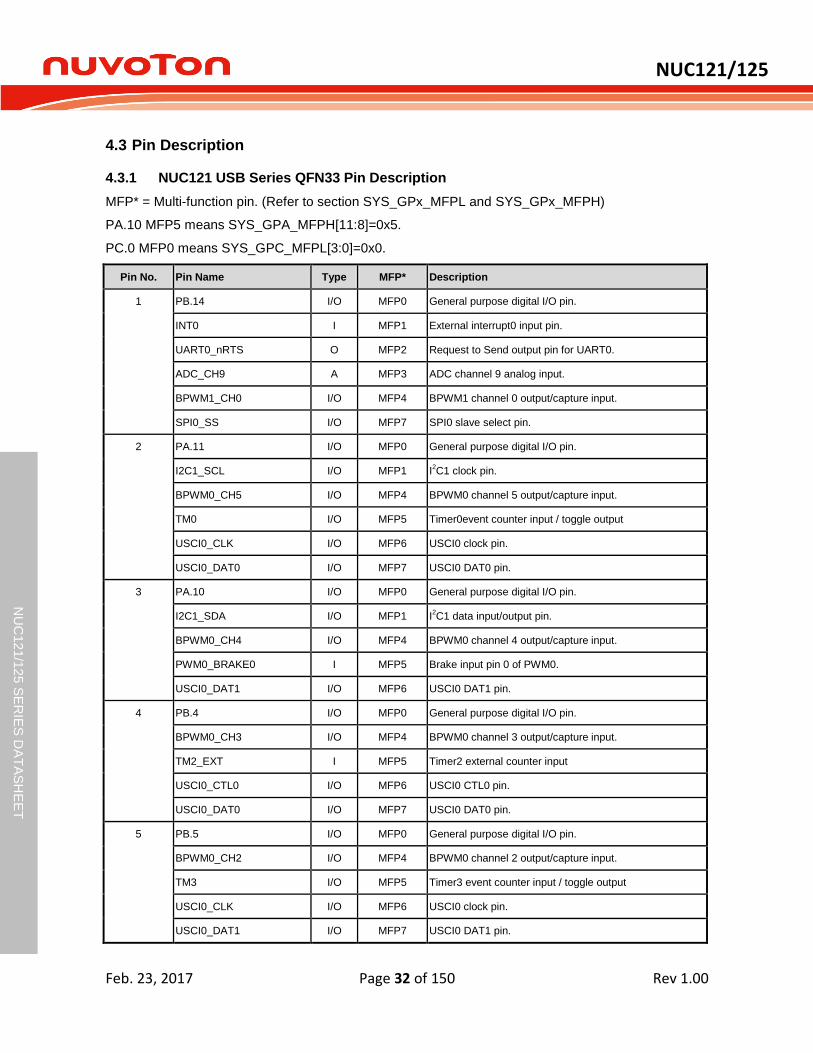
NUC121/125
Feb. 23, 2017 Page 32 of 150 Rev 1.00
NU
C12
1/1
25 S
ER
IES
DA
TA
SH
EE
T
Pin Description 4.3
4.3.1 NUC121 USB Series QFN33 Pin Description
MFP* = Multi-function pin. (Refer to section SYS_GPx_MFPL and SYS_GPx_MFPH)
PA.10 MFP5 means SYS_GPA_MFPH[11:8]=0x5.
PC.0 MFP0 means SYS_GPC_MFPL[3:0]=0x0.
Pin No. Pin Name Type MFP* Description
1 PB.14 I/O MFP0 General purpose digital I/O pin.
INT0 I MFP1 External interrupt0 input pin.
UART0_nRTS O MFP2 Request to Send output pin for UART0.
ADC_CH9 A MFP3 ADC channel 9 analog input.
BPWM1_CH0 I/O MFP4 BPWM1 channel 0 output/capture input.
SPI0_SS I/O MFP7 SPI0 slave select pin.
2 PA.11 I/O MFP0 General purpose digital I/O pin.
I2C1_SCL I/O MFP1 I2C1 clock pin.
BPWM0_CH5 I/O MFP4 BPWM0 channel 5 output/capture input.
TM0 I/O MFP5 Timer0event counter input / toggle output
USCI0_CLK I/O MFP6 USCI0 clock pin.
USCI0_DAT0 I/O MFP7 USCI0 DAT0 pin.
3 PA.10 I/O MFP0 General purpose digital I/O pin.
I2C1_SDA I/O MFP1 I2C1 data input/output pin.
BPWM0_CH4 I/O MFP4 BPWM0 channel 4 output/capture input.
PWM0_BRAKE0 I MFP5 Brake input pin 0 of PWM0.
USCI0_DAT1 I/O MFP6 USCI0 DAT1 pin.
4 PB.4 I/O MFP0 General purpose digital I/O pin.
BPWM0_CH3 I/O MFP4 BPWM0 channel 3 output/capture input.
TM2_EXT I MFP5 Timer2 external counter input
USCI0_CTL0 I/O MFP6 USCI0 CTL0 pin.
USCI0_DAT0 I/O MFP7 USCI0 DAT0 pin.
5 PB.5 I/O MFP0 General purpose digital I/O pin.
BPWM0_CH2 I/O MFP4 BPWM0 channel 2 output/capture input.
TM3 I/O MFP5 Timer3 event counter input / toggle output
USCI0_CLK I/O MFP6 USCI0 clock pin.
USCI0_DAT1 I/O MFP7 USCI0 DAT1 pin.
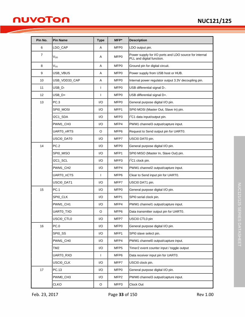
NUC121/125
Feb. 23, 2017 Page 33 of 150 Rev 1.00
NU
C12
1/1
25 S
ER
IES
DA
TA
SH
EE
T
Pin No. Pin Name Type MFP* Description
6 LDO_CAP A MFP0 LDO output pin.
7 VDD A MFP0
Power supply for I/O ports and LDO source for internal PLL and digital function.
8 VSS A MFP0 Ground pin for digital circuit.
9 USB_VBUS A MFP0 Power supply from USB host or HUB.
10 USB_VDD33_CAP A MFP0 Internal power regulator output 3.3V decoupling pin.
11 USB_D- I MFP0 USB differential signal D-.
12 USB_D+ I MFP0 USB differential signal D+.
13 PC.3 I/O MFP0 General purpose digital I/O pin.
SPI0_MOSI I/O MFP1 SPI0 MOSI (Master Out, Slave In) pin.
I2C1_SDA I/O MFP3 I2C1 data input/output pin.
PWM1_CH3 I/O MFP4 PWM1 channel3 output/capture input.
UART0_nRTS O MFP6 Request to Send output pin for UART0.
USCI0_DAT0 I/O MFP7 USCI0 DAT0 pin.
14 PC.2 I/O MFP0 General purpose digital I/O pin.
SPI0_MISO I/O MFP1 SPI0 MISO (Master In, Slave Out) pin.
I2C1_SCL I/O MFP3 I2C1 clock pin.
PWM1_CH2 I/O MFP4 PWM1 channel2 output/capture input.
UART0_nCTS I MFP6 Clear to Send input pin for UART0.
USCI0_DAT1 I/O MFP7 USCI0 DAT1 pin.
15 PC.1 I/O MFP0 General purpose digital I/O pin.
SPI0_CLK I/O MFP1 SPI0 serial clock pin.
PWM1_CH1 I/O MFP4 PWM1 channel1 output/capture input.
UART0_TXD O MFP6 Data transmitter output pin for UART0.
USCI0_CTL0 I/O MFP7 USCI0 CTL0 pin
16 PC.0 I/O MFP0 General purpose digital I/O pin.
SPI0_SS I/O MFP1 SPI0 slave select pin.
PWM1_CH0 I/O MFP4 PWM1 channel0 output/capture input.
TM2 I/O MFP5 Timer2 event counter input / toggle output
UART0_RXD I MFP6 Data receiver input pin for UART0.
USCI0_CLK I/O MFP7 USCI0 clock pin.
17 PC.13 I/O MFP0 General purpose digital I/O pin.
PWM0_CH3 I/O MFP2 PWM0 channel3 output/capture input.
CLKO O MFP3 Clock Out
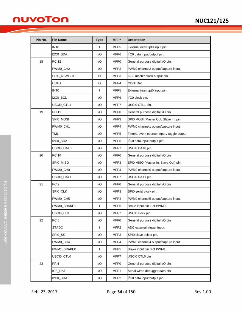
NUC121/125
Feb. 23, 2017 Page 34 of 150 Rev 1.00
NU
C12
1/1
25 S
ER
IES
DA
TA
SH
EE
T
Pin No. Pin Name Type MFP* Description
INT0 I MFP5 External interrupt0 input pin.
I2C0_SDA I/O MFP6 I2C0 data input/output pin.
18 PC.12 I/O MFP0 General purpose digital I/O pin.
PWM0_CH2 I/O MFP2 PWM0 channel2 output/capture input.
SPI0_I2SMCLK O MFP3 I2S0 master clock output pin.
CLKO O MFP4 Clock Out
INT0 I MFP5 External interrupt0 input pin.
I2C0_SCL I/O MFP6 I2C0 clock pin.
USCI0_CTL1 I/O MFP7 USCI0 CTL1 pin.
19 PC.11 I/O MFP0 General purpose digital I/O pin.
SPI0_MOSI I/O MFP3 SPI0 MOSI (Master Out, Slave In) pin.
PWM0_CH1 I/O MFP4 PWM0 channel1 output/capture input.
TM1 I/O MFP5 Timer1 event counter input / toggle output
I2C0_SDA I/O MFP6 I2C0 data input/output pin.
USCI0_DAT0 I/O MFP7 USCI0 DAT0 pin.
20 PC.10 I/O MFP0 General purpose digital I/O pin.
SPI0_MISO I/O MFP3 SPI0 MISO (Master In, Slave Out) pin.
PWM0_CH0 I/O MFP4 PWM0 channel0 output/capture input.
USCI0_DAT1 I/O MFP7 USCI0 DAT1 pin.
21 PC.9 I/O MFP0 General purpose digital I/O pin.
SPI0_CLK I/O MFP3 SPI0 serial clock pin.
PWM0_CH5 I/O MFP4 PWM0 channel5 output/capture input.
PWM0_BRAKE1 I MFP5 Brake input pin 1 of PWM0.
USCI0_CLK I/O MFP7 USCI0 clock pin
22 PC.8 I/O MFP0 General purpose digital I/O pin.
STADC I MFP2 ADC external trigger input.
SPI0_SS I/O MFP3 SPI0 slave select pin.
PWM0_CH4 I/O MFP4 PWM0 channel4 output/capture input.
PWM1_BRAKE0 I MFP5 Brake input pin 0 of PWM1.
USCI0_CTL0 I/O MFP7 USCI0 CTL0 pin
23 PF.4 I/O MFP0 General purpose digital I/O pin.
ICE_DAT I/O MFP1 Serial wired debugger data pin
I2C0_SDA I/O MFP2 I2C0 data input/output pin.
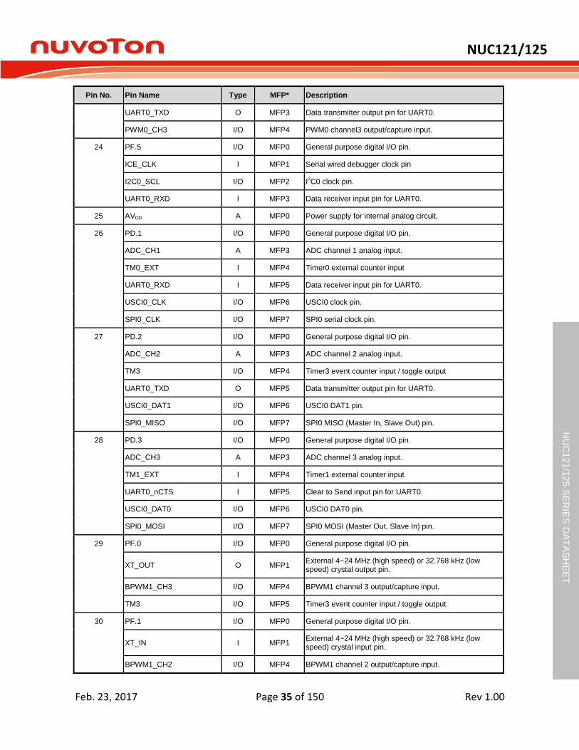
NUC121/125
Feb. 23, 2017 Page 35 of 150 Rev 1.00
NU
C12
1/1
25 S
ER
IES
DA
TA
SH
EE
T
Pin No. Pin Name Type MFP* Description
UART0_TXD O MFP3 Data transmitter output pin for UART0.
PWM0_CH3 I/O MFP4 PWM0 channel3 output/capture input.
24 PF.5 I/O MFP0 General purpose digital I/O pin.
ICE_CLK I MFP1 Serial wired debugger clock pin
I2C0_SCL I/O MFP2 I2C0 clock pin.
UART0_RXD I MFP3 Data receiver input pin for UART0.
25 AVDD A MFP0 Power supply for internal analog circuit.
26 PD.1 I/O MFP0 General purpose digital I/O pin.
ADC_CH1 A MFP3 ADC channel 1 analog input.
TM0_EXT I MFP4 Timer0 external counter input
UART0_RXD I MFP5 Data receiver input pin for UART0.
USCI0_CLK I/O MFP6 USCI0 clock pin.
SPI0_CLK I/O MFP7 SPI0 serial clock pin.
27 PD.2 I/O MFP0 General purpose digital I/O pin.
ADC_CH2 A MFP3 ADC channel 2 analog input.
TM3 I/O MFP4 Timer3 event counter input / toggle output
UART0_TXD O MFP5 Data transmitter output pin for UART0.
USCI0_DAT1 I/O MFP6 USCI0 DAT1 pin.
SPI0_MISO I/O MFP7 SPI0 MISO (Master In, Slave Out) pin.
28 PD.3 I/O MFP0 General purpose digital I/O pin.
ADC_CH3 A MFP3 ADC channel 3 analog input.
TM1_EXT I MFP4 Timer1 external counter input
UART0_nCTS I MFP5 Clear to Send input pin for UART0.
USCI0_DAT0 I/O MFP6 USCI0 DAT0 pin.
SPI0_MOSI I/O MFP7 SPI0 MOSI (Master Out, Slave In) pin.
29 PF.0 I/O MFP0 General purpose digital I/O pin.
XT_OUT O MFP1 External 4~24 MHz (high speed) or 32.768 kHz (low speed) crystal output pin.
BPWM1_CH3 I/O MFP4 BPWM1 channel 3 output/capture input.
TM3 I/O MFP5 Timer3 event counter input / toggle output
30 PF.1 I/O MFP0 General purpose digital I/O pin.
XT_IN I MFP1 External 4~24 MHz (high speed) or 32.768 kHz (low speed) crystal input pin.
BPWM1_CH2 I/O MFP4 BPWM1 channel 2 output/capture input.
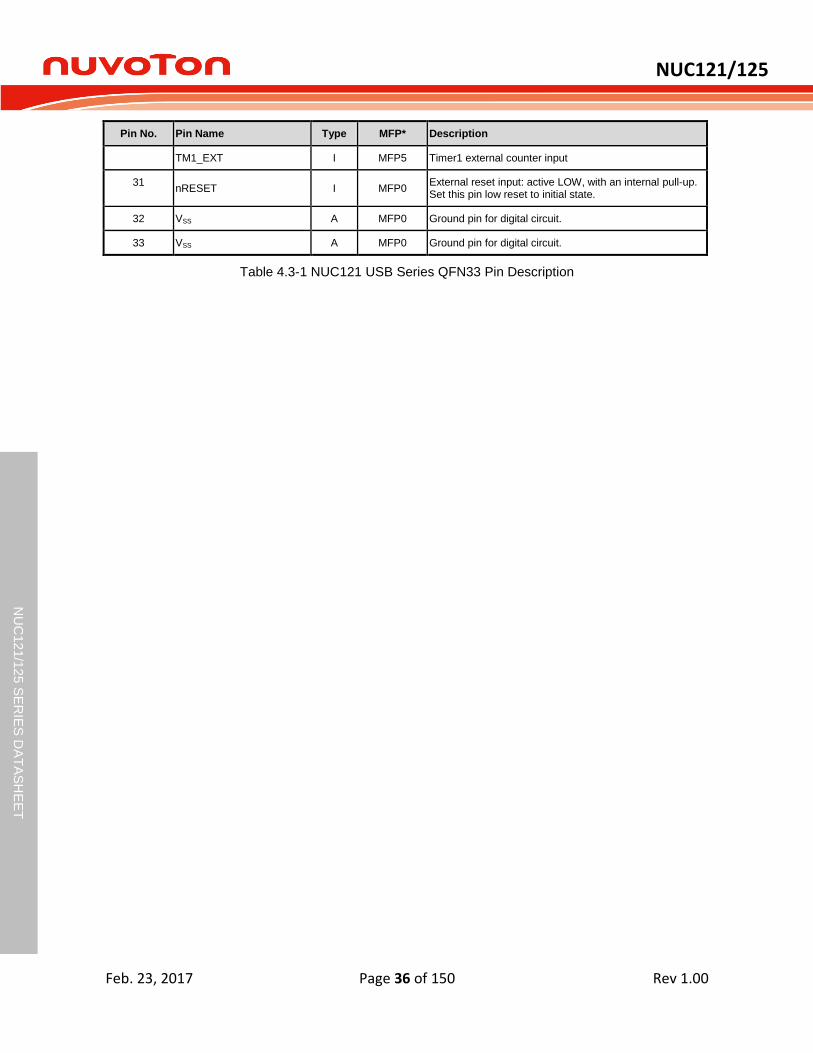
NUC121/125
Feb. 23, 2017 Page 36 of 150 Rev 1.00
NU
C12
1/1
25 S
ER
IES
DA
TA
SH
EE
T
Pin No. Pin Name Type MFP* Description
TM1_EXT I MFP5 Timer1 external counter input
31 nRESET I MFP0
External reset input: active LOW, with an internal pull-up. Set this pin low reset to initial state.
32 VSS A MFP0 Ground pin for digital circuit.
33 VSS A MFP0 Ground pin for digital circuit.
Table 4.3-1 NUC121 USB Series QFN33 Pin Description
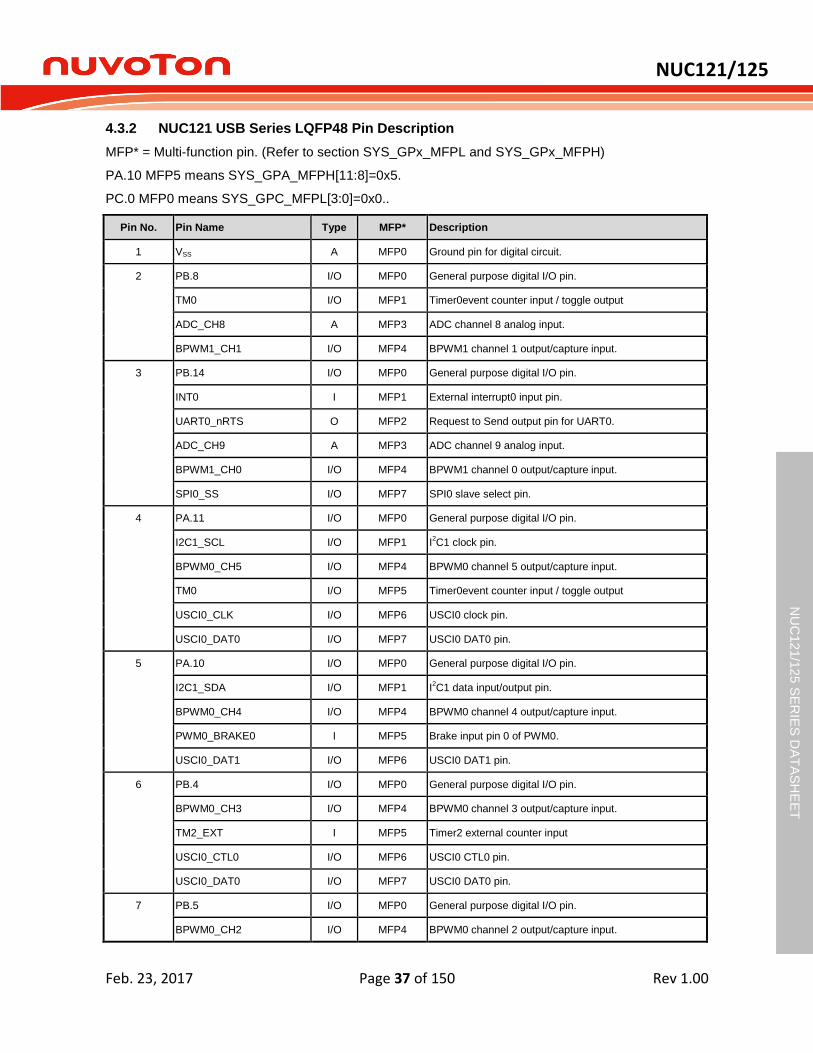
NUC121/125
Feb. 23, 2017 Page 37 of 150 Rev 1.00
NU
C12
1/1
25 S
ER
IES
DA
TA
SH
EE
T
4.3.2 NUC121 USB Series LQFP48 Pin Description
MFP* = Multi-function pin. (Refer to section SYS_GPx_MFPL and SYS_GPx_MFPH)
PA.10 MFP5 means SYS_GPA_MFPH[11:8]=0x5.
PC.0 MFP0 means SYS_GPC_MFPL[3:0]=0x0..
Pin No. Pin Name Type MFP* Description
1 VSS A MFP0 Ground pin for digital circuit.
2 PB.8 I/O MFP0 General purpose digital I/O pin.
TM0 I/O MFP1 Timer0event counter input / toggle output
ADC_CH8 A MFP3 ADC channel 8 analog input.
BPWM1_CH1 I/O MFP4 BPWM1 channel 1 output/capture input.
3 PB.14 I/O MFP0 General purpose digital I/O pin.
INT0 I MFP1 External interrupt0 input pin.
UART0_nRTS O MFP2 Request to Send output pin for UART0.
ADC_CH9 A MFP3 ADC channel 9 analog input.
BPWM1_CH0 I/O MFP4 BPWM1 channel 0 output/capture input.
SPI0_SS I/O MFP7 SPI0 slave select pin.
4 PA.11 I/O MFP0 General purpose digital I/O pin.
I2C1_SCL I/O MFP1 I2C1 clock pin.
BPWM0_CH5 I/O MFP4 BPWM0 channel 5 output/capture input.
TM0 I/O MFP5 Timer0event counter input / toggle output
USCI0_CLK I/O MFP6 USCI0 clock pin.
USCI0_DAT0 I/O MFP7 USCI0 DAT0 pin.
5 PA.10 I/O MFP0 General purpose digital I/O pin.
I2C1_SDA I/O MFP1 I2C1 data input/output pin.
BPWM0_CH4 I/O MFP4 BPWM0 channel 4 output/capture input.
PWM0_BRAKE0 I MFP5 Brake input pin 0 of PWM0.
USCI0_DAT1 I/O MFP6 USCI0 DAT1 pin.
6 PB.4 I/O MFP0 General purpose digital I/O pin.
BPWM0_CH3 I/O MFP4 BPWM0 channel 3 output/capture input.
TM2_EXT I MFP5 Timer2 external counter input
USCI0_CTL0 I/O MFP6 USCI0 CTL0 pin.
USCI0_DAT0 I/O MFP7 USCI0 DAT0 pin.
7 PB.5 I/O MFP0 General purpose digital I/O pin.
BPWM0_CH2 I/O MFP4 BPWM0 channel 2 output/capture input.
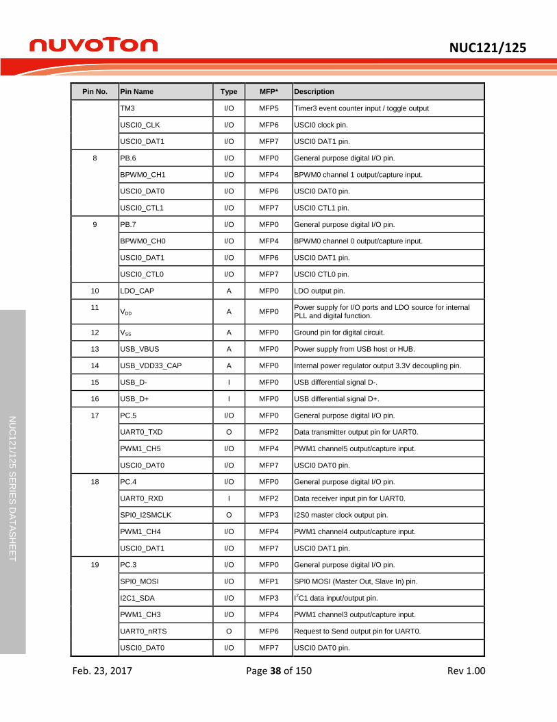
NUC121/125
Feb. 23, 2017 Page 38 of 150 Rev 1.00
NU
C12
1/1
25 S
ER
IES
DA
TA
SH
EE
T
Pin No. Pin Name Type MFP* Description
TM3 I/O MFP5 Timer3 event counter input / toggle output
USCI0_CLK I/O MFP6 USCI0 clock pin.
USCI0_DAT1 I/O MFP7 USCI0 DAT1 pin.
8 PB.6 I/O MFP0 General purpose digital I/O pin.
BPWM0_CH1 I/O MFP4 BPWM0 channel 1 output/capture input.
USCI0_DAT0 I/O MFP6 USCI0 DAT0 pin.
USCI0_CTL1 I/O MFP7 USCI0 CTL1 pin.
9 PB.7 I/O MFP0 General purpose digital I/O pin.
BPWM0_CH0 I/O MFP4 BPWM0 channel 0 output/capture input.
USCI0_DAT1 I/O MFP6 USCI0 DAT1 pin.
USCI0_CTL0 I/O MFP7 USCI0 CTL0 pin.
10 LDO_CAP A MFP0 LDO output pin.
11 VDD A MFP0
Power supply for I/O ports and LDO source for internal PLL and digital function.
12 VSS A MFP0 Ground pin for digital circuit.
13 USB_VBUS A MFP0 Power supply from USB host or HUB.
14 USB_VDD33_CAP A MFP0 Internal power regulator output 3.3V decoupling pin.
15 USB_D- I MFP0 USB differential signal D-.
16 USB_D+ I MFP0 USB differential signal D+.
17 PC.5 I/O MFP0 General purpose digital I/O pin.
UART0_TXD O MFP2 Data transmitter output pin for UART0.
PWM1_CH5 I/O MFP4 PWM1 channel5 output/capture input.
USCI0_DAT0 I/O MFP7 USCI0 DAT0 pin.
18 PC.4 I/O MFP0 General purpose digital I/O pin.
UART0_RXD I MFP2 Data receiver input pin for UART0.
SPI0_I2SMCLK O MFP3 I2S0 master clock output pin.
PWM1_CH4 I/O MFP4 PWM1 channel4 output/capture input.
USCI0_DAT1 I/O MFP7 USCI0 DAT1 pin.
19 PC.3 I/O MFP0 General purpose digital I/O pin.
SPI0_MOSI I/O MFP1 SPI0 MOSI (Master Out, Slave In) pin.
I2C1_SDA I/O MFP3 I2C1 data input/output pin.
PWM1_CH3 I/O MFP4 PWM1 channel3 output/capture input.
UART0_nRTS O MFP6 Request to Send output pin for UART0.
USCI0_DAT0 I/O MFP7 USCI0 DAT0 pin.

NUC121/125
Feb. 23, 2017 Page 39 of 150 Rev 1.00
NU
C12
1/1
25 S
ER
IES
DA
TA
SH
EE
T
Pin No. Pin Name Type MFP* Description
20 PC.2 I/O MFP0 General purpose digital I/O pin.
SPI0_MISO I/O MFP1 SPI0 MISO (Master In, Slave Out) pin.
I2C1_SCL I/O MFP3 I2C1 clock pin.
PWM1_CH2 I/O MFP4 PWM1 channel2 output/capture input.
UART0_nCTS I MFP6 Clear to Send input pin for UART0.
USCI0_DAT1 I/O MFP7 USCI0 DAT1 pin.
21 PC.1 I/O MFP0 General purpose digital I/O pin.
SPI0_CLK I/O MFP1 SPI0 serial clock pin.
PWM1_CH1 I/O MFP4 PWM1 channel1 output/capture input.
UART0_TXD O MFP6 Data transmitter output pin for UART0.
USCI0_CTL0 I/O MFP7 USCI0 CTL0 pin
22 PC.0 I/O MFP0 General purpose digital I/O pin.
SPI0_SS I/O MFP1 SPI0 slave select pin.
PWM1_CH0 I/O MFP4 PWM1 channel0 output/capture input.
TM2 I/O MFP5 Timer2 event counter input / toggle output
UART0_RXD I MFP6 Data receiver input pin for UART0.
USCI0_CLK I/O MFP7 USCI0 clock pin.
23 PB.10 I/O MFP0 General purpose digital I/O pin.
TM2 I/O MFP1 Timer2 event counter input / toggle output
SPI0_I2SMCLK O MFP3 I2S0 master clock output pin.
PWM0_CH5 I/O MFP4 PWM0 channel5 output/capture input.
24 PB.9 I/O MFP0 General purpose digital I/O pin.
TM1 I/O MFP1 Timer1 event counter input / toggle output
SPI0_I2SMCLK O MFP3 I2S0 master clock output pin.
PWM0_CH4 I/O MFP4 PWM0 channel4 output/capture input.
25 PC.13 I/O MFP0 General purpose digital I/O pin.
PWM0_CH3 I/O MFP2 PWM0 channel3 output/capture input.
CLKO O MFP3 Clock Out
INT0 I MFP5 External interrupt0 input pin.
I2C0_SDA I/O MFP6 I2C0 data input/output pin.
26 PC.12 I/O MFP0 General purpose digital I/O pin.
PWM0_CH2 I/O MFP2 PWM0 channel2 output/capture input.
SPI0_I2SMCLK O MFP3 I2S0 master clock output pin.
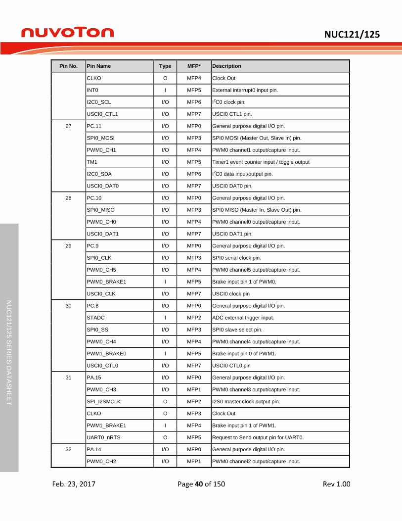
NUC121/125
Feb. 23, 2017 Page 40 of 150 Rev 1.00
NU
C12
1/1
25 S
ER
IES
DA
TA
SH
EE
T
Pin No. Pin Name Type MFP* Description
CLKO O MFP4 Clock Out
INT0 I MFP5 External interrupt0 input pin.
I2C0_SCL I/O MFP6 I2C0 clock pin.
USCI0_CTL1 I/O MFP7 USCI0 CTL1 pin.
27 PC.11 I/O MFP0 General purpose digital I/O pin.
SPI0_MOSI I/O MFP3 SPI0 MOSI (Master Out, Slave In) pin.
PWM0_CH1 I/O MFP4 PWM0 channel1 output/capture input.
TM1 I/O MFP5 Timer1 event counter input / toggle output
I2C0_SDA I/O MFP6 I2C0 data input/output pin.
USCI0_DAT0 I/O MFP7 USCI0 DAT0 pin.
28 PC.10 I/O MFP0 General purpose digital I/O pin.
SPI0_MISO I/O MFP3 SPI0 MISO (Master In, Slave Out) pin.
PWM0_CH0 I/O MFP4 PWM0 channel0 output/capture input.
USCI0_DAT1 I/O MFP7 USCI0 DAT1 pin.
29 PC.9 I/O MFP0 General purpose digital I/O pin.
SPI0_CLK I/O MFP3 SPI0 serial clock pin.
PWM0_CH5 I/O MFP4 PWM0 channel5 output/capture input.
PWM0_BRAKE1 I MFP5 Brake input pin 1 of PWM0.
USCI0_CLK I/O MFP7 USCI0 clock pin
30 PC.8 I/O MFP0 General purpose digital I/O pin.
STADC I MFP2 ADC external trigger input.
SPI0_SS I/O MFP3 SPI0 slave select pin.
PWM0_CH4 I/O MFP4 PWM0 channel4 output/capture input.
PWM1_BRAKE0 I MFP5 Brake input pin 0 of PWM1.
USCI0_CTL0 I/O MFP7 USCI0 CTL0 pin
31 PA.15 I/O MFP0 General purpose digital I/O pin.
PWM0_CH3 I/O MFP1 PWM0 channel3 output/capture input.
SPI_I2SMCLK O MFP2 I2S0 master clock output pin.
CLKO O MFP3 Clock Out
PWM1_BRAKE1 I MFP4 Brake input pin 1 of PWM1.
UART0_nRTS O MFP5 Request to Send output pin for UART0.
32 PA.14 I/O MFP0 General purpose digital I/O pin.
PWM0_CH2 I/O MFP1 PWM0 channel2 output/capture input.
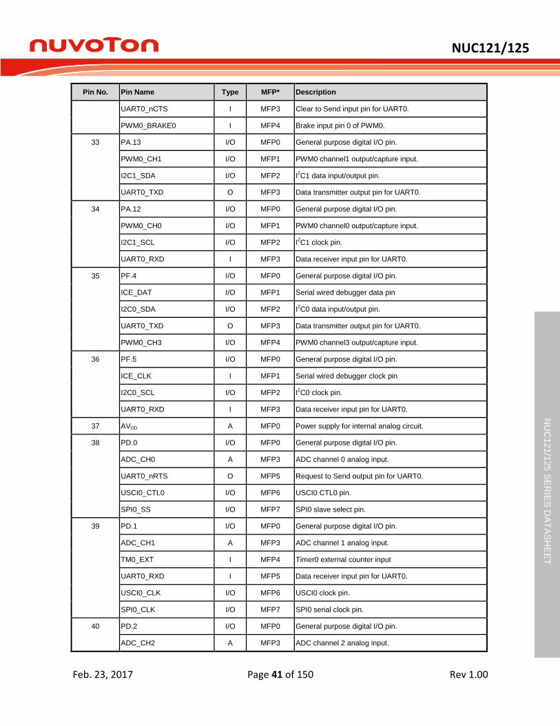
NUC121/125
Feb. 23, 2017 Page 41 of 150 Rev 1.00
NU
C12
1/1
25 S
ER
IES
DA
TA
SH
EE
T
Pin No. Pin Name Type MFP* Description
UART0_nCTS I MFP3 Clear to Send input pin for UART0.
PWM0_BRAKE0 I MFP4 Brake input pin 0 of PWM0.
33 PA.13 I/O MFP0 General purpose digital I/O pin.
PWM0_CH1 I/O MFP1 PWM0 channel1 output/capture input.
I2C1_SDA I/O MFP2 I2C1 data input/output pin.
UART0_TXD O MFP3 Data transmitter output pin for UART0.
34 PA.12 I/O MFP0 General purpose digital I/O pin.
PWM0_CH0 I/O MFP1 PWM0 channel0 output/capture input.
I2C1_SCL I/O MFP2 I2C1 clock pin.
UART0_RXD I MFP3 Data receiver input pin for UART0.
35 PF.4 I/O MFP0 General purpose digital I/O pin.
ICE_DAT I/O MFP1 Serial wired debugger data pin
I2C0_SDA I/O MFP2 I2C0 data input/output pin.
UART0_TXD O MFP3 Data transmitter output pin for UART0.
PWM0_CH3 I/O MFP4 PWM0 channel3 output/capture input.
36 PF.5 I/O MFP0 General purpose digital I/O pin.
ICE_CLK I MFP1 Serial wired debugger clock pin
I2C0_SCL I/O MFP2 I2C0 clock pin.
UART0_RXD I MFP3 Data receiver input pin for UART0.
37 AVDD A MFP0 Power supply for internal analog circuit.
38 PD.0 I/O MFP0 General purpose digital I/O pin.
ADC_CH0 A MFP3 ADC channel 0 analog input.
UART0_nRTS O MFP5 Request to Send output pin for UART0.
USCI0_CTL0 I/O MFP6 USCI0 CTL0 pin.
SPI0_SS I/O MFP7 SPI0 slave select pin.
39 PD.1 I/O MFP0 General purpose digital I/O pin.
ADC_CH1 A MFP3 ADC channel 1 analog input.
TM0_EXT I MFP4 Timer0 external counter input
UART0_RXD I MFP5 Data receiver input pin for UART0.
USCI0_CLK I/O MFP6 USCI0 clock pin.
SPI0_CLK I/O MFP7 SPI0 serial clock pin.
40 PD.2 I/O MFP0 General purpose digital I/O pin.
ADC_CH2 A MFP3 ADC channel 2 analog input.

NUC121/125
Feb. 23, 2017 Page 42 of 150 Rev 1.00
NU
C12
1/1
25 S
ER
IES
DA
TA
SH
EE
T
Pin No. Pin Name Type MFP* Description
TM3 I/O MFP4 Timer3 event counter input / toggle output
UART0_TXD O MFP5 Data transmitter output pin for UART0.
USCI0_DAT1 I/O MFP6 USCI0 DAT1 pin.
SPI0_MISO I/O MFP7 SPI0 MISO (Master In, Slave Out) pin.
41 PD.3 I/O MFP0 General purpose digital I/O pin.
ADC_CH3 A MFP3 ADC channel 3 analog input.
TM1_EXT I MFP4 Timer1 external counter input
UART0_nCTS I MFP5 Clear to Send input pin for UART0.
USCI0_DAT0 I/O MFP6 USCI0 DAT0 pin.
SPI0_MOSI I/O MFP7 SPI0 MOSI (Master Out, Slave In) pin.
42 PD.4 I/O MFP0 General purpose digital I/O pin.
ADC_CH4 A MFP2 ADC channel 4 analog input.
BPWM1_CH5 I/O MFP4 BPWM1 channel 5 output/capture input.
UART0_nRTS O MFP5 Request to Send output pin for UART0.
USCI0_CTL0 I/O MFP6 USCI0 CTL0 pin.
SPI0_SS I/O MFP7 SPI0 slave select pin.
43 PD.5 I/O MFP0 General purpose digital I/O pin.
ADC_CH5 A MFP2 ADC channel 5 analog input.
BPWM1_CH4 I/O MFP4 BPWM1 channel 4 output/capture input.
44 PF.0 I/O MFP0 General purpose digital I/O pin.
XT_OUT O MFP1 External 4~24 MHz (high speed) or 32.768 kHz (low speed) crystal output pin.
BPWM1_CH3 I/O MFP4 BPWM1 channel 3 output/capture input.
TM3 I/O MFP5 Timer3 event counter input / toggle output
45 PF.1 I/O MFP0 General purpose digital I/O pin.
XT_IN I MFP1 External 4~24 MHz (high speed) or 32.768 kHz (low speed) crystal input pin.
BPWM1_CH2 I/O MFP4 BPWM1 channel 2 output/capture input.
TM1_EXT I MFP5 Timer1 external counter input
46 nRESET I MFP0
External reset input: active LOW, with an internal pull-up. Set this pin low reset to initial state.
47 PF.2 I/O MFP0 General purpose digital I/O pin.
ICE_DAT I/O MFP1 Serial wired debugger data pin
I2C0_SDA I/O MFP2 I2C0 data input/output pin.
ADC_CH6 A MFP3 ADC channel 6 analog input.
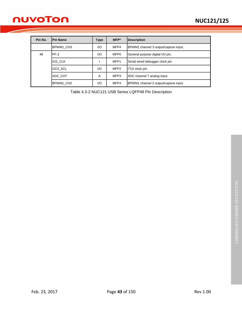
NUC121/125
Feb. 23, 2017 Page 43 of 150 Rev 1.00
NU
C12
1/1
25 S
ER
IES
DA
TA
SH
EE
T
Pin No. Pin Name Type MFP* Description
BPWM1_CH3 I/O MFP4 BPWM1 channel 3 output/capture input.
48 PF.3 I/O MFP0 General purpose digital I/O pin.
ICE_CLK I MFP1 Serial wired debugger clock pin
I2C0_SCL I/O MFP2 I2C0 clock pin.
ADC_CH7 A MFP3 ADC channel 7 analog input.
BPWM1_CH2 I/O MFP4 BPWM1 channel 2 output/capture input.
Table 4.3-2 NUC121 USB Series LQFP48 Pin Description

NUC121/125
Feb. 23, 2017 Page 44 of 150 Rev 1.00
NU
C12
1/1
25 S
ER
IES
DA
TA
SH
EE
T
4.3.3 NUC121 USB Series LQFP64 Pin Description
MFP* = Multi-function pin. (Refer to section SYS_GPx_MFPL and SYS_GPx_MFPH)
PA.10 MFP5 means SYS_GPA_MFPH[11:8]=0x5.
PC.0 MFP0 means SYS_GPC_MFPL[3:0]=0x0.
Pin No. Pin Name Type MFP* Description
1 PB.14 I/O MFP0 General purpose digital I/O pin.
INT0 I MFP1 External interrupt0 input pin.
UART0_nRTS O MFP2 Request to Send output pin for UART0.
ADC_CH9 A MFP3 ADC channel 9 analog input.
BPWM1_CH0 I/O MFP4 BPWM1 channel 0 output/capture input.
SPI0_SS I/O MFP7 SPI0 slave select pin.
2 PB.13 I/O MFP0 General purpose digital I/O pin.
ADC_CH10 A MFP3 ADC channel 10 analog input.
USCI0_CTL1 I/O MFP6 USCI0 CTL1 pin.
3 PB.12 I/O MFP0 General purpose digital I/O pin.
CLKO O MFP2 Clock Out
ADC_CH11 A MFP3 ADC channel 11 analog input.
USCI0_CTL0 I/O MFP6 USCI0 CTL0 pin.
4 PA.11 I/O MFP0 General purpose digital I/O pin.
I2C1_SCL I/O MFP1 I2C1 clock pin.
BPWM0_CH5 I/O MFP4 BPWM0 channel 5 output/capture input.
TM0 I/O MFP5 Timer0event counter input / toggle output
USCI0_CLK I/O MFP6 USCI0 clock pin.
USCI0_DAT0 I/O MFP7 USCI0 DAT0 pin.
5 PA.10 I/O MFP0 General purpose digital I/O pin.
I2C1_SDA I/O MFP1 I2C1 data input/output pin.
BPWM0_CH4 I/O MFP4 BPWM0 channel 4 output/capture input.
PWM0_BRAKE0 I MFP5 Brake input pin 0 of PWM0.
USCI0_DAT1 I/O MFP6 USCI0 DAT1 pin.
6 PD.8 I/O MFP0 General purpose digital I/O pin.
USCI0_DAT0 I/O MFP6 USCI0 DAT0 pin.
7 PD.9 I/O MFP0 General purpose digital I/O pin.
PWM0_BRAKE1 I MFP5 Brake input pin 1 of PWM0.
8 PD.10 I/O MFP0 General purpose digital I/O pin.

NUC121/125
Feb. 23, 2017 Page 45 of 150 Rev 1.00
NU
C12
1/1
25 S
ER
IES
DA
TA
SH
EE
T
Pin No. Pin Name Type MFP* Description
CLKO O MFP1 Clock Out
BPWM0_CH5 I/O MFP4 BPWM0 channel 5 output/capture input.
9 PD.11 I/O MFP0 General purpose digital I/O pin.
INT1 I MFP1 External interrupt1 input pin.
BPWM0_CH4 I/O MFP4 BPWM0 channel 4 output/capture input.
10 PB.4 I/O MFP0 General purpose digital I/O pin.
BPWM0_CH3 I/O MFP4 BPWM0 channel 3 output/capture input.
TM2_EXT I MFP5 Timer2 external counter input
USCI0_CTL0 I/O MFP6 USCI0 CTL0 pin.
USCI0_DAT0 I/O MFP7 USCI0 DAT0 pin.
11 PB.5 I/O MFP0 General purpose digital I/O pin.
BPWM0_CH2 I/O MFP4 BPWM0 channel 2 output/capture input.
TM3 I/O MFP5 Timer3 event counter input / toggle output
USCI0_CLK I/O MFP6 USCI0 clock pin.
USCI0_DAT1 I/O MFP7 USCI0 DAT1 pin.
12 PB.6 I/O MFP0 General purpose digital I/O pin.
BPWM0_CH1 I/O MFP4 BPWM0 channel 1 output/capture input.
USCI0_DAT0 I/O MFP6 USCI0 DAT0 pin.
USCI0_CTL1 I/O MFP7 USCI0 CTL1 pin.
13 PB.7 I/O MFP0 General purpose digital I/O pin.
BPWM0_CH0 I/O MFP4 BPWM0 channel 0 output/capture input.
USCI0_DAT1 I/O MFP6 USCI0 DAT1 pin.
USCI0_CTL0 I/O MFP7 USCI0 CTL0 pin.
14 LDO_CAP A MFP0 LDO output pin.
15 VDD A MFP0
Power supply for I/O ports and LDO source for internal PLL and digital function.
16 VSS A MFP0 Ground pin for digital circuit.
17 USB_VBUS A MFP0 Power supply from USB host or HUB.
18 USB_VDD33_CAP A MFP0 Internal power regulator output 3.3V decoupling pin.
19 USB_D- I MFP0 USB differential signal D-.
20 USB_D+ I MFP0 USB differential signal D+.
21 PB.0 I/O MFP0 General purpose digital I/O pin.
UART0_RXD I MFP1 Data receiver input pin for UART0.
PWM1_CH0 I/O MFP4 PWM1 channel0 output/capture input.

NUC121/125
Feb. 23, 2017 Page 46 of 150 Rev 1.00
NU
C12
1/1
25 S
ER
IES
DA
TA
SH
EE
T
Pin No. Pin Name Type MFP* Description
22 PB.1 I/O MFP0 General purpose digital I/O pin.
UART0_TXD O MFP1 Data transmitter output pin for UART0.
PWM1_CH1 I/O MFP4 PWM1 channel1 output/capture input.
23 PB.2 I/O MFP0 General purpose digital I/O pin.
UART0_nRTS O MFP1 Request to Send output pin for UART0.
TM2_EXT I MFP2 Timer2 external counter input
PWM1_CH2 I/O MFP4 PWM1 channel2 output/capture input.
24 PB.3 I/O MFP0 General purpose digital I/O pin.
UART0_nCTS I MFP1 Clear to Send input pin for UART0.
TM3_EXT I MFP2 Timer3 external counter input
PWM1_CH3 I/O MFP4 PWM1 channel3 output/capture input.
25 PC.5 I/O MFP0 General purpose digital I/O pin.
UART0_TXD O MFP2 Data transmitter output pin for UART0.
PWM1_CH5 I/O MFP4 PWM1 channel5 output/capture input.
USCI0_DAT0 I/O MFP7 USCI0 DAT0 pin.
26 PC.4 I/O MFP0 General purpose digital I/O pin.
UART0_RXD I MFP2 Data receiver input pin for UART0.
SPI0_I2SMCLK O MFP3 I2S0 master clock output pin.
PWM1_CH4 I/O MFP4 PWM1 channel4 output/capture input.
USCI0_DAT1 I/O MFP7 USCI0 DAT1 pin.
27 PC.3 I/O MFP0 General purpose digital I/O pin.
SPI0_MOSI I/O MFP1 SPI0 MOSI (Master Out, Slave In) pin.
I2C1_SDA I/O MFP3 I2C1 data input/output pin.
PWM1_CH3 I/O MFP4 PWM1 channel3 output/capture input.
UART0_nRTS O MFP6 Request to Send output pin for UART0.
USCI0_DAT0 I/O MFP7 USCI0 DAT0 pin.
28 PC.2 I/O MFP0 General purpose digital I/O pin.
SPI0_MISO I/O MFP1 SPI0 MISO (Master In, Slave Out) pin.
I2C1_SCL I/O MFP3 I2C1 clock pin.
PWM1_CH2 I/O MFP4 PWM1 channel2 output/capture input.
UART0_nCTS I MFP6 Clear to Send input pin for UART0.
USCI0_DAT1 I/O MFP7 USCI0 DAT1 pin.
29 PC.1 I/O MFP0 General purpose digital I/O pin.

NUC121/125
Feb. 23, 2017 Page 47 of 150 Rev 1.00
NU
C12
1/1
25 S
ER
IES
DA
TA
SH
EE
T
Pin No. Pin Name Type MFP* Description
SPI0_CLK I/O MFP1 SPI0 serial clock pin.
PWM1_CH1 I/O MFP4 PWM1 channel1 output/capture input.
UART0_TXD O MFP6 Data transmitter output pin for UART0.
USCI0_CTL0 I/O MFP7 USCI0 CTL0 pin
30 PC.0 I/O MFP0 General purpose digital I/O pin.
SPI0_SS I/O MFP1 SPI0 slave select pin.
PWM1_CH0 I/O MFP4 PWM1 channel0 output/capture input.
TM2 I/O MFP5 Timer2 event counter input / toggle output
UART0_RXD I MFP6 Data receiver input pin for UART0.
USCI0_CLK I/O MFP7 USCI0 clock pin.
31 PB.10 I/O MFP0 General purpose digital I/O pin.
TM2 I/O MFP1 Timer2 event counter input / toggle output
SPI0_I2SMCLK O MFP3 I2S0 master clock output pin.
PWM0_CH5 I/O MFP4 PWM0 channel5 output/capture input.
32 PB.9 I/O MFP0 General purpose digital I/O pin.
TM1 I/O MFP1 Timer1 event counter input / toggle output
SPI0_I2SMCLK O MFP3 I2S0 master clock output pin.
PWM0_CH4 I/O MFP4 PWM0 channel4 output/capture input.
33 PE.2 I/O MFP0 General purpose digital I/O pin.
INT1 I MFP1 External interrupt1 input pin.
TM0_EXT I MFP5 Timer0 external counter input
I2C0_SCL I/O MFP6 I2C0 clock pin.
USCI0_CTL1 I/O MFP7 USCI0 CTL1 pin.
34 PC.13 I/O MFP0 General purpose digital I/O pin.
PWM0_CH3 I/O MFP2 PWM0 channel3 output/capture input.
CLKO O MFP3 Clock Out
INT0 I MFP5 External interrupt0 input pin.
I2C0_SDA I/O MFP6 I2C0 data input/output pin.
35 PC.12 I/O MFP0 General purpose digital I/O pin.
PWM0_CH2 I/O MFP2 PWM0 channel2 output/capture input.
SPI0_I2SMCLK O MFP3 I2S0 master clock output pin.
CLKO O MFP4 Clock Out
INT0 I MFP5 External interrupt0 input pin.
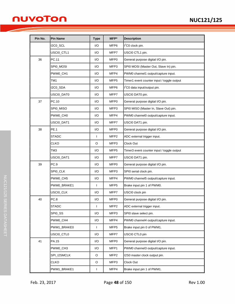
NUC121/125
Feb. 23, 2017 Page 48 of 150 Rev 1.00
NU
C12
1/1
25 S
ER
IES
DA
TA
SH
EE
T
Pin No. Pin Name Type MFP* Description
I2C0_SCL I/O MFP6 I2C0 clock pin.
USCI0_CTL1 I/O MFP7 USCI0 CTL1 pin.
36 PC.11 I/O MFP0 General purpose digital I/O pin.
SPI0_MOSI I/O MFP3 SPI0 MOSI (Master Out, Slave In) pin.
PWM0_CH1 I/O MFP4 PWM0 channel1 output/capture input.
TM1 I/O MFP5 Timer1 event counter input / toggle output
I2C0_SDA I/O MFP6 I2C0 data input/output pin.
USCI0_DAT0 I/O MFP7 USCI0 DAT0 pin.
37 PC.10 I/O MFP0 General purpose digital I/O pin.
SPI0_MISO I/O MFP3 SPI0 MISO (Master In, Slave Out) pin.
PWM0_CH0 I/O MFP4 PWM0 channel0 output/capture input.
USCI0_DAT1 I/O MFP7 USCI0 DAT1 pin.
38 PE.1 I/O MFP0 General purpose digital I/O pin.
STADC I MFP2 ADC external trigger input.
CLKO O MFP3 Clock Out
TM3 I/O MFP5 Timer3 event counter input / toggle output
USCI0_DAT1 I/O MFP7 USCI0 DAT1 pin.
39 PC.9 I/O MFP0 General purpose digital I/O pin.
SPI0_CLK I/O MFP3 SPI0 serial clock pin.
PWM0_CH5 I/O MFP4 PWM0 channel5 output/capture input.
PWM0_BRAKE1 I MFP5 Brake input pin 1 of PWM0.
USCI0_CLK I/O MFP7 USCI0 clock pin
40 PC.8 I/O MFP0 General purpose digital I/O pin.
STADC I MFP2 ADC external trigger input.
SPI0_SS I/O MFP3 SPI0 slave select pin.
PWM0_CH4 I/O MFP4 PWM0 channel4 output/capture input.
PWM1_BRAKE0 I MFP5 Brake input pin 0 of PWM1.
USCI0_CTL0 I/O MFP7 USCI0 CTL0 pin
41 PA.15 I/O MFP0 General purpose digital I/O pin.
PWM0_CH3 I/O MFP1 PWM0 channel3 output/capture input.
SPI_I2SMCLK O MFP2 I2S0 master clock output pin.
CLKO O MFP3 Clock Out
PWM1_BRAKE1 I MFP4 Brake input pin 1 of PWM1.

NUC121/125
Feb. 23, 2017 Page 49 of 150 Rev 1.00
NU
C12
1/1
25 S
ER
IES
DA
TA
SH
EE
T
Pin No. Pin Name Type MFP* Description
UART0_nRTS O MFP5 Request to Send output pin for UART0.
42 PE.0 I/O MFP0 General purpose digital I/O pin.
INT0 I MFP1 External interrupt0 input pin.
CLKO O MFP3 Clock Out
PWM0_CH3 I/O MFP4 PWM0 channel3 output/capture input.
TM1_EXT I MFP5 Timer1 external counter input
USCI0_DAT0 I/O MFP7 USCI0 DAT0 pin.
43 PA.14 I/O MFP0 General purpose digital I/O pin.
PWM0_CH2 I/O MFP1 PWM0 channel2 output/capture input.
UART0_nCTS I MFP3 Clear to Send input pin for UART0.
PWM0_BRAKE0 I MFP4 Brake input pin 0 of PWM0.
44 PA.13 I/O MFP0 General purpose digital I/O pin.
PWM0_CH1 I/O MFP1 PWM0 channel1 output/capture input.
I2C1_SDA I/O MFP2 I2C1 data input/output pin.
UART0_TXD O MFP3 Data transmitter output pin for UART0.
45 PA.12 I/O MFP0 General purpose digital I/O pin.
PWM0_CH0 I/O MFP1 PWM0 channel0 output/capture input.
I2C1_SCL I/O MFP2 I2C1 clock pin.
UART0_RXD I MFP3 Data receiver input pin for UART0.
46 PF.4 I/O MFP0 General purpose digital I/O pin.
ICE_DAT I/O MFP1 Serial wired debugger data pin
I2C0_SDA I/O MFP2 I2C0 data input/output pin.
UART0_TXD O MFP3 Data transmitter output pin for UART0.
PWM0_CH3 I/O MFP4 PWM0 channel3 output/capture input.
47 PF.5 I/O MFP0 General purpose digital I/O pin.
ICE_CLK I MFP1 Serial wired debugger clock pin
I2C0_SCL I/O MFP2 I2C0 clock pin.
UART0_RXD I MFP3 Data receiver input pin for UART0.
48 AVDD A MFP0 Power supply for internal analog circuit.
49 PD.0 I/O MFP0 General purpose digital I/O pin.
ADC_CH0 A MFP3 ADC channel 0 analog input.
UART0_nRTS O MFP5 Request to Send output pin for UART0.
USCI0_CTL0 I/O MFP6 USCI0 CTL0 pin.
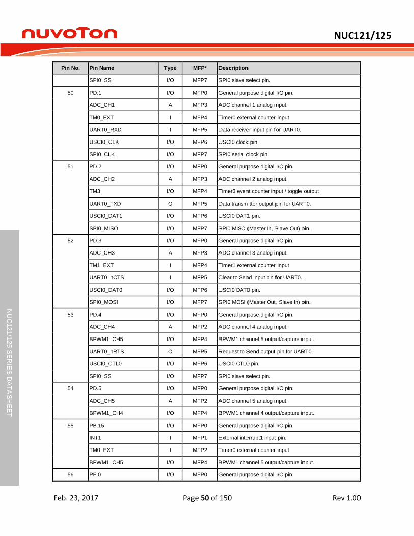
NUC121/125
Feb. 23, 2017 Page 50 of 150 Rev 1.00
NU
C12
1/1
25 S
ER
IES
DA
TA
SH
EE
T
Pin No. Pin Name Type MFP* Description
SPI0_SS I/O MFP7 SPI0 slave select pin.
50 PD.1 I/O MFP0 General purpose digital I/O pin.
ADC_CH1 A MFP3 ADC channel 1 analog input.
TM0_EXT I MFP4 Timer0 external counter input
UART0_RXD I MFP5 Data receiver input pin for UART0.
USCI0_CLK I/O MFP6 USCI0 clock pin.
SPI0_CLK I/O MFP7 SPI0 serial clock pin.
51 PD.2 I/O MFP0 General purpose digital I/O pin.
ADC_CH2 A MFP3 ADC channel 2 analog input.
TM3 I/O MFP4 Timer3 event counter input / toggle output
UART0_TXD O MFP5 Data transmitter output pin for UART0.
USCI0_DAT1 I/O MFP6 USCI0 DAT1 pin.
SPI0_MISO I/O MFP7 SPI0 MISO (Master In, Slave Out) pin.
52 PD.3 I/O MFP0 General purpose digital I/O pin.
ADC_CH3 A MFP3 ADC channel 3 analog input.
TM1_EXT I MFP4 Timer1 external counter input
UART0_nCTS I MFP5 Clear to Send input pin for UART0.
USCI0_DAT0 I/O MFP6 USCI0 DAT0 pin.
SPI0_MOSI I/O MFP7 SPI0 MOSI (Master Out, Slave In) pin.
53 PD.4 I/O MFP0 General purpose digital I/O pin.
ADC_CH4 A MFP2 ADC channel 4 analog input.
BPWM1_CH5 I/O MFP4 BPWM1 channel 5 output/capture input.
UART0_nRTS O MFP5 Request to Send output pin for UART0.
USCI0_CTL0 I/O MFP6 USCI0 CTL0 pin.
SPI0_SS I/O MFP7 SPI0 slave select pin.
54 PD.5 I/O MFP0 General purpose digital I/O pin.
ADC_CH5 A MFP2 ADC channel 5 analog input.
BPWM1_CH4 I/O MFP4 BPWM1 channel 4 output/capture input.
55 PB.15 I/O MFP0 General purpose digital I/O pin.
INT1 I MFP1 External interrupt1 input pin.
TM0_EXT I MFP2 Timer0 external counter input
BPWM1_CH5 I/O MFP4 BPWM1 channel 5 output/capture input.
56 PF.0 I/O MFP0 General purpose digital I/O pin.
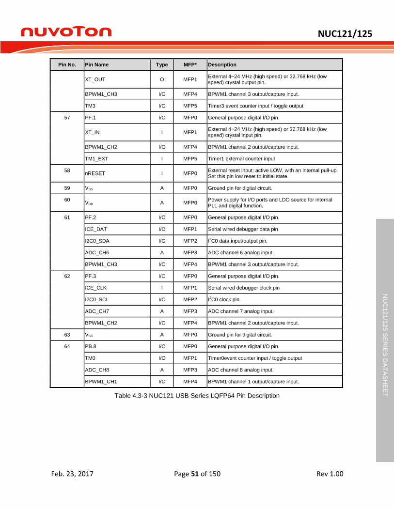
NUC121/125
Feb. 23, 2017 Page 51 of 150 Rev 1.00
NU
C12
1/1
25 S
ER
IES
DA
TA
SH
EE
T
Pin No. Pin Name Type MFP* Description
XT_OUT O MFP1 External 4~24 MHz (high speed) or 32.768 kHz (low speed) crystal output pin.
BPWM1_CH3 I/O MFP4 BPWM1 channel 3 output/capture input.
TM3 I/O MFP5 Timer3 event counter input / toggle output
57 PF.1 I/O MFP0 General purpose digital I/O pin.
XT_IN I MFP1 External 4~24 MHz (high speed) or 32.768 kHz (low speed) crystal input pin.
BPWM1_CH2 I/O MFP4 BPWM1 channel 2 output/capture input.
TM1_EXT I MFP5 Timer1 external counter input
58 nRESET I MFP0
External reset input: active LOW, with an internal pull-up. Set this pin low reset to initial state.
59 VSS A MFP0 Ground pin for digital circuit.
60 VDD A MFP0
Power supply for I/O ports and LDO source for internal PLL and digital function.
61 PF.2 I/O MFP0 General purpose digital I/O pin.
ICE_DAT I/O MFP1 Serial wired debugger data pin
I2C0_SDA I/O MFP2 I2C0 data input/output pin.
ADC_CH6 A MFP3 ADC channel 6 analog input.
BPWM1_CH3 I/O MFP4 BPWM1 channel 3 output/capture input.
62 PF.3 I/O MFP0 General purpose digital I/O pin.
ICE_CLK I MFP1 Serial wired debugger clock pin
I2C0_SCL I/O MFP2 I2C0 clock pin.
ADC_CH7 A MFP3 ADC channel 7 analog input.
BPWM1_CH2 I/O MFP4 BPWM1 channel 2 output/capture input.
63 VSS A MFP0 Ground pin for digital circuit.
64 PB.8 I/O MFP0 General purpose digital I/O pin.
TM0 I/O MFP1 Timer0event counter input / toggle output
ADC_CH8 A MFP3 ADC channel 8 analog input.
BPWM1_CH1 I/O MFP4 BPWM1 channel 1 output/capture input.
Table 4.3-3 NUC121 USB Series LQFP64 Pin Description
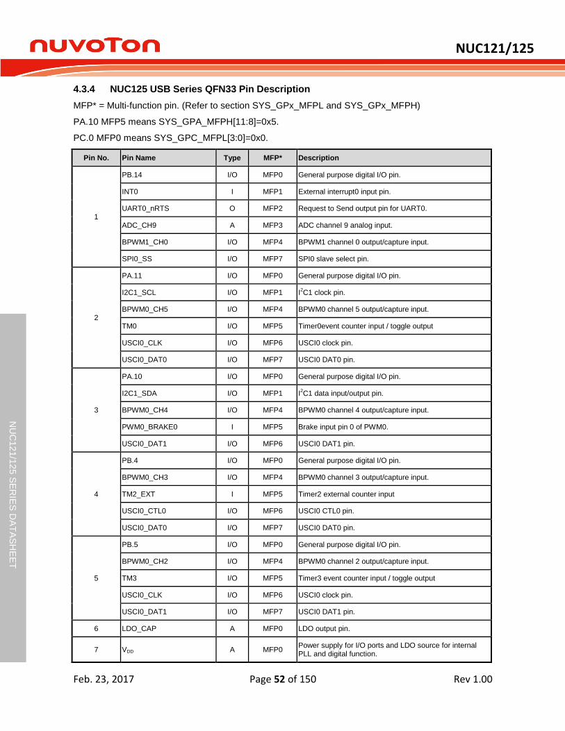
NUC121/125
Feb. 23, 2017 Page 52 of 150 Rev 1.00
NU
C12
1/1
25 S
ER
IES
DA
TA
SH
EE
T
4.3.4 NUC125 USB Series QFN33 Pin Description
MFP* = Multi-function pin. (Refer to section SYS_GPx_MFPL and SYS_GPx_MFPH)
PA.10 MFP5 means SYS_GPA_MFPH[11:8]=0x5.
PC.0 MFP0 means SYS_GPC_MFPL[3:0]=0x0.
Pin No. Pin Name Type MFP* Description
1
PB.14 I/O MFP0 General purpose digital I/O pin.
INT0 I MFP1 External interrupt0 input pin.
UART0_nRTS O MFP2 Request to Send output pin for UART0.
ADC_CH9 A MFP3 ADC channel 9 analog input.
BPWM1_CH0 I/O MFP4 BPWM1 channel 0 output/capture input.
SPI0_SS I/O MFP7 SPI0 slave select pin.
2
PA.11 I/O MFP0 General purpose digital I/O pin.
I2C1_SCL I/O MFP1 I2C1 clock pin.
BPWM0_CH5 I/O MFP4 BPWM0 channel 5 output/capture input.
TM0 I/O MFP5 Timer0event counter input / toggle output
USCI0_CLK I/O MFP6 USCI0 clock pin.
USCI0_DAT0 I/O MFP7 USCI0 DAT0 pin.
3
PA.10 I/O MFP0 General purpose digital I/O pin.
I2C1_SDA I/O MFP1 I2C1 data input/output pin.
BPWM0_CH4 I/O MFP4 BPWM0 channel 4 output/capture input.
PWM0_BRAKE0 I MFP5 Brake input pin 0 of PWM0.
USCI0_DAT1 I/O MFP6 USCI0 DAT1 pin.
4
PB.4 I/O MFP0 General purpose digital I/O pin.
BPWM0_CH3 I/O MFP4 BPWM0 channel 3 output/capture input.
TM2_EXT I MFP5 Timer2 external counter input
USCI0_CTL0 I/O MFP6 USCI0 CTL0 pin.
USCI0_DAT0 I/O MFP7 USCI0 DAT0 pin.
5
PB.5 I/O MFP0 General purpose digital I/O pin.
BPWM0_CH2 I/O MFP4 BPWM0 channel 2 output/capture input.
TM3 I/O MFP5 Timer3 event counter input / toggle output
USCI0_CLK I/O MFP6 USCI0 clock pin.
USCI0_DAT1 I/O MFP7 USCI0 DAT1 pin.
6 LDO_CAP A MFP0 LDO output pin.
7 VDD A MFP0 Power supply for I/O ports and LDO source for internal PLL and digital function.
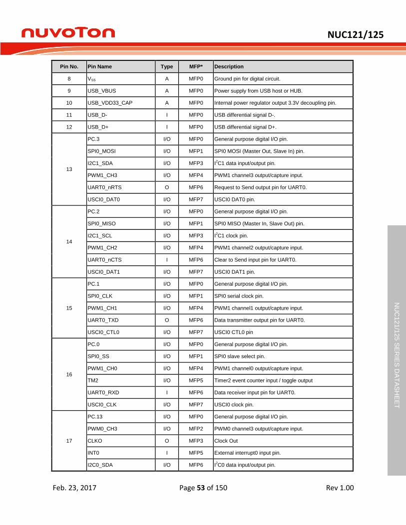
NUC121/125
Feb. 23, 2017 Page 53 of 150 Rev 1.00
NU
C12
1/1
25 S
ER
IES
DA
TA
SH
EE
T
Pin No. Pin Name Type MFP* Description
8 VSS A MFP0 Ground pin for digital circuit.
9 USB_VBUS A MFP0 Power supply from USB host or HUB.
10 USB_VDD33_CAP A MFP0 Internal power regulator output 3.3V decoupling pin.
11 USB_D- I MFP0 USB differential signal D-.
12 USB_D+ I MFP0 USB differential signal D+.
13
PC.3 I/O MFP0 General purpose digital I/O pin.
SPI0_MOSI I/O MFP1 SPI0 MOSI (Master Out, Slave In) pin.
I2C1_SDA I/O MFP3 I2C1 data input/output pin.
PWM1_CH3 I/O MFP4 PWM1 channel3 output/capture input.
UART0_nRTS O MFP6 Request to Send output pin for UART0.
USCI0_DAT0 I/O MFP7 USCI0 DAT0 pin.
14
PC.2 I/O MFP0 General purpose digital I/O pin.
SPI0_MISO I/O MFP1 SPI0 MISO (Master In, Slave Out) pin.
I2C1_SCL I/O MFP3 I2C1 clock pin.
PWM1_CH2 I/O MFP4 PWM1 channel2 output/capture input.
UART0_nCTS I MFP6 Clear to Send input pin for UART0.
USCI0_DAT1 I/O MFP7 USCI0 DAT1 pin.
15
PC.1 I/O MFP0 General purpose digital I/O pin.
SPI0_CLK I/O MFP1 SPI0 serial clock pin.
PWM1_CH1 I/O MFP4 PWM1 channel1 output/capture input.
UART0_TXD O MFP6 Data transmitter output pin for UART0.
USCI0_CTL0 I/O MFP7 USCI0 CTL0 pin
16
PC.0 I/O MFP0 General purpose digital I/O pin.
SPI0_SS I/O MFP1 SPI0 slave select pin.
PWM1_CH0 I/O MFP4 PWM1 channel0 output/capture input.
TM2 I/O MFP5 Timer2 event counter input / toggle output
UART0_RXD I MFP6 Data receiver input pin for UART0.
USCI0_CLK I/O MFP7 USCI0 clock pin.
17
PC.13 I/O MFP0 General purpose digital I/O pin.
PWM0_CH3 I/O MFP2 PWM0 channel3 output/capture input.
CLKO O MFP3 Clock Out
INT0 I MFP5 External interrupt0 input pin.
I2C0_SDA I/O MFP6 I2C0 data input/output pin.
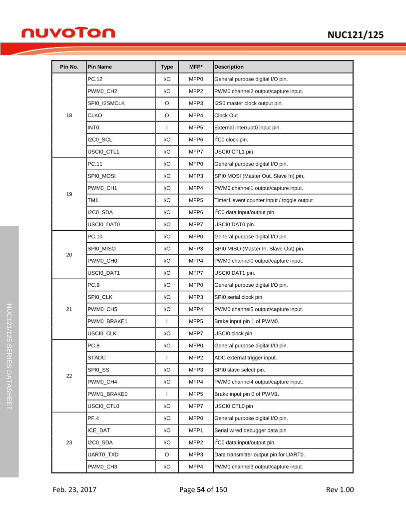
NUC121/125
Feb. 23, 2017 Page 54 of 150 Rev 1.00
NU
C12
1/1
25 S
ER
IES
DA
TA
SH
EE
T
Pin No. Pin Name Type MFP* Description
18
PC.12 I/O MFP0 General purpose digital I/O pin.
PWM0_CH2 I/O MFP2 PWM0 channel2 output/capture input.
SPI0_I2SMCLK O MFP3 I2S0 master clock output pin.
CLKO O MFP4 Clock Out
INT0 I MFP5 External interrupt0 input pin.
I2C0_SCL I/O MFP6 I2C0 clock pin.
USCI0_CTL1 I/O MFP7 USCI0 CTL1 pin.
19
PC.11 I/O MFP0 General purpose digital I/O pin.
SPI0_MOSI I/O MFP3 SPI0 MOSI (Master Out, Slave In) pin.
PWM0_CH1 I/O MFP4 PWM0 channel1 output/capture input.
TM1 I/O MFP5 Timer1 event counter input / toggle output
I2C0_SDA I/O MFP6 I2C0 data input/output pin.
USCI0_DAT0 I/O MFP7 USCI0 DAT0 pin.
20
PC.10 I/O MFP0 General purpose digital I/O pin.
SPI0_MISO I/O MFP3 SPI0 MISO (Master In, Slave Out) pin.
PWM0_CH0 I/O MFP4 PWM0 channel0 output/capture input.
USCI0_DAT1 I/O MFP7 USCI0 DAT1 pin.
21
PC.9 I/O MFP0 General purpose digital I/O pin.
SPI0_CLK I/O MFP3 SPI0 serial clock pin.
PWM0_CH5 I/O MFP4 PWM0 channel5 output/capture input.
PWM0_BRAKE1 I MFP5 Brake input pin 1 of PWM0.
USCI0_CLK I/O MFP7 USCI0 clock pin
22
PC.8 I/O MFP0 General purpose digital I/O pin.
STADC I MFP2 ADC external trigger input.
SPI0_SS I/O MFP3 SPI0 slave select pin.
PWM0_CH4 I/O MFP4 PWM0 channel4 output/capture input.
PWM1_BRAKE0 I MFP5 Brake input pin 0 of PWM1.
USCI0_CTL0 I/O MFP7 USCI0 CTL0 pin
23
PF.4 I/O MFP0 General purpose digital I/O pin.
ICE_DAT I/O MFP1 Serial wired debugger data pin
I2C0_SDA I/O MFP2 I2C0 data input/output pin.
UART0_TXD O MFP3 Data transmitter output pin for UART0.
PWM0_CH3 I/O MFP4 PWM0 channel3 output/capture input.
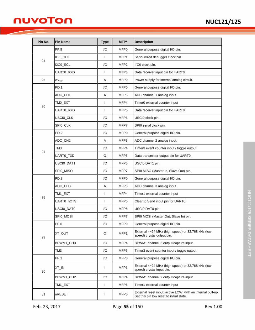
NUC121/125
Feb. 23, 2017 Page 55 of 150 Rev 1.00
NU
C12
1/1
25 S
ER
IES
DA
TA
SH
EE
T
Pin No. Pin Name Type MFP* Description
24
PF.5 I/O MFP0 General purpose digital I/O pin.
ICE_CLK I MFP1 Serial wired debugger clock pin
I2C0_SCL I/O MFP2 I2C0 clock pin.
UART0_RXD I MFP3 Data receiver input pin for UART0.
25 AVDD A MFP0 Power supply for internal analog circuit.
26
PD.1 I/O MFP0 General purpose digital I/O pin.
ADC_CH1 A MFP3 ADC channel 1 analog input.
TM0_EXT I MFP4 Timer0 external counter input
UART0_RXD I MFP5 Data receiver input pin for UART0.
USCI0_CLK I/O MFP6 USCI0 clock pin.
SPI0_CLK I/O MFP7 SPI0 serial clock pin.
27
PD.2 I/O MFP0 General purpose digital I/O pin.
ADC_CH2 A MFP3 ADC channel 2 analog input.
TM3 I/O MFP4 Timer3 event counter input / toggle output
UART0_TXD O MFP5 Data transmitter output pin for UART0.
USCI0_DAT1 I/O MFP6 USCI0 DAT1 pin.
SPI0_MISO I/O MFP7 SPI0 MISO (Master In, Slave Out) pin.
28
PD.3 I/O MFP0 General purpose digital I/O pin.
ADC_CH3 A MFP3 ADC channel 3 analog input.
TM1_EXT I MFP4 Timer1 external counter input
UART0_nCTS I MFP5 Clear to Send input pin for UART0.
USCI0_DAT0 I/O MFP6 USCI0 DAT0 pin.
SPI0_MOSI I/O MFP7 SPI0 MOSI (Master Out, Slave In) pin.
29
PF.0 I/O MFP0 General purpose digital I/O pin.
XT_OUT O MFP1 External 4~24 MHz (high speed) or 32.768 kHz (low speed) crystal output pin.
BPWM1_CH3 I/O MFP4 BPWM1 channel 3 output/capture input.
TM3 I/O MFP5 Timer3 event counter input / toggle output
30
PF.1 I/O MFP0 General purpose digital I/O pin.
XT_IN I MFP1 External 4~24 MHz (high speed) or 32.768 kHz (low speed) crystal input pin.
BPWM1_CH2 I/O MFP4 BPWM1 channel 2 output/capture input.
TM1_EXT I MFP5 Timer1 external counter input
31 nRESET I MFP0 External reset input: active LOW, with an internal pull-up. Set this pin low reset to initial state.

NUC121/125
Feb. 23, 2017 Page 56 of 150 Rev 1.00
NU
C12
1/1
25 S
ER
IES
DA
TA
SH
EE
T
Pin No. Pin Name Type MFP* Description
32 VDDIO A MFP0 Power supply for PB.14, PA.11, PA.10, PB.4 and PB.5.
33 VSS A MFP0 Ground pin for digital circuit.
Table 4.3-4 NUC125 USB Series QFN33 Pin Description
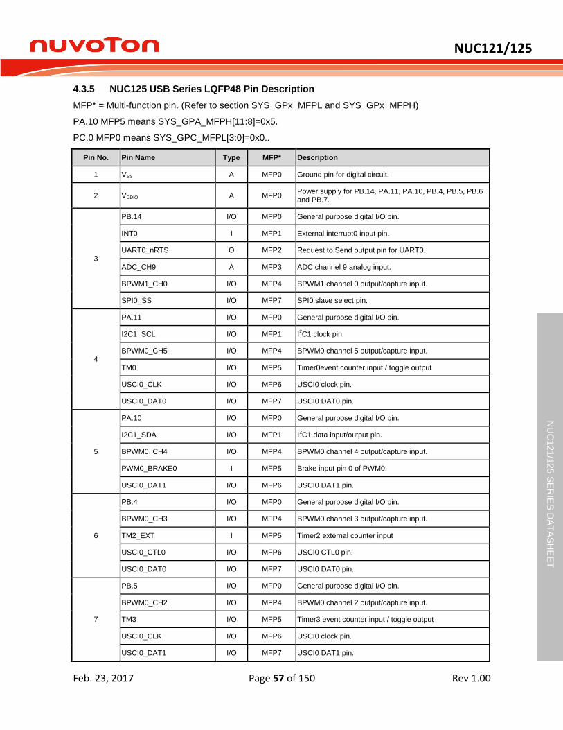
NUC121/125
Feb. 23, 2017 Page 57 of 150 Rev 1.00
NU
C12
1/1
25 S
ER
IES
DA
TA
SH
EE
T
4.3.5 NUC125 USB Series LQFP48 Pin Description
MFP* = Multi-function pin. (Refer to section SYS_GPx_MFPL and SYS_GPx_MFPH)
PA.10 MFP5 means SYS_GPA_MFPH[11:8]=0x5.
PC.0 MFP0 means SYS_GPC_MFPL[3:0]=0x0..
Pin No. Pin Name Type MFP* Description
1 VSS A MFP0 Ground pin for digital circuit.
2 VDDIO A MFP0 Power supply for PB.14, PA.11, PA.10, PB.4, PB.5, PB.6 and PB.7.
3
PB.14 I/O MFP0 General purpose digital I/O pin.
INT0 I MFP1 External interrupt0 input pin.
UART0_nRTS O MFP2 Request to Send output pin for UART0.
ADC_CH9 A MFP3 ADC channel 9 analog input.
BPWM1_CH0 I/O MFP4 BPWM1 channel 0 output/capture input.
SPI0_SS I/O MFP7 SPI0 slave select pin.
4
PA.11 I/O MFP0 General purpose digital I/O pin.
I2C1_SCL I/O MFP1 I2C1 clock pin.
BPWM0_CH5 I/O MFP4 BPWM0 channel 5 output/capture input.
TM0 I/O MFP5 Timer0event counter input / toggle output
USCI0_CLK I/O MFP6 USCI0 clock pin.
USCI0_DAT0 I/O MFP7 USCI0 DAT0 pin.
5
PA.10 I/O MFP0 General purpose digital I/O pin.
I2C1_SDA I/O MFP1 I2C1 data input/output pin.
BPWM0_CH4 I/O MFP4 BPWM0 channel 4 output/capture input.
PWM0_BRAKE0 I MFP5 Brake input pin 0 of PWM0.
USCI0_DAT1 I/O MFP6 USCI0 DAT1 pin.
6
PB.4 I/O MFP0 General purpose digital I/O pin.
BPWM0_CH3 I/O MFP4 BPWM0 channel 3 output/capture input.
TM2_EXT I MFP5 Timer2 external counter input
USCI0_CTL0 I/O MFP6 USCI0 CTL0 pin.
USCI0_DAT0 I/O MFP7 USCI0 DAT0 pin.
7
PB.5 I/O MFP0 General purpose digital I/O pin.
BPWM0_CH2 I/O MFP4 BPWM0 channel 2 output/capture input.
TM3 I/O MFP5 Timer3 event counter input / toggle output
USCI0_CLK I/O MFP6 USCI0 clock pin.
USCI0_DAT1 I/O MFP7 USCI0 DAT1 pin.
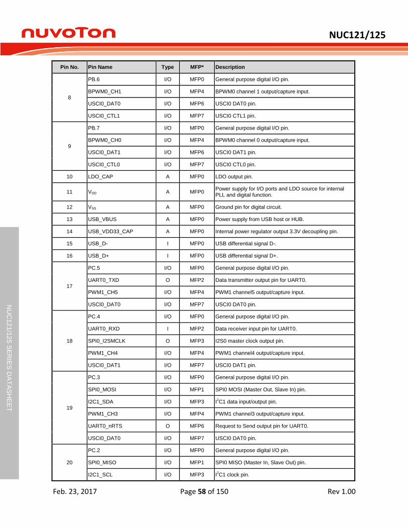
NUC121/125
Feb. 23, 2017 Page 58 of 150 Rev 1.00
NU
C12
1/1
25 S
ER
IES
DA
TA
SH
EE
T
Pin No. Pin Name Type MFP* Description
8
PB.6 I/O MFP0 General purpose digital I/O pin.
BPWM0_CH1 I/O MFP4 BPWM0 channel 1 output/capture input.
USCI0_DAT0 I/O MFP6 USCI0 DAT0 pin.
USCI0_CTL1 I/O MFP7 USCI0 CTL1 pin.
9
PB.7 I/O MFP0 General purpose digital I/O pin.
BPWM0_CH0 I/O MFP4 BPWM0 channel 0 output/capture input.
USCI0_DAT1 I/O MFP6 USCI0 DAT1 pin.
USCI0_CTL0 I/O MFP7 USCI0 CTL0 pin.
10 LDO_CAP A MFP0 LDO output pin.
11 VDD A MFP0 Power supply for I/O ports and LDO source for internal PLL and digital function.
12 VSS A MFP0 Ground pin for digital circuit.
13 USB_VBUS A MFP0 Power supply from USB host or HUB.
14 USB_VDD33_CAP A MFP0 Internal power regulator output 3.3V decoupling pin.
15 USB_D- I MFP0 USB differential signal D-.
16 USB_D+ I MFP0 USB differential signal D+.
17
PC.5 I/O MFP0 General purpose digital I/O pin.
UART0_TXD O MFP2 Data transmitter output pin for UART0.
PWM1_CH5 I/O MFP4 PWM1 channel5 output/capture input.
USCI0_DAT0 I/O MFP7 USCI0 DAT0 pin.
18
PC.4 I/O MFP0 General purpose digital I/O pin.
UART0_RXD I MFP2 Data receiver input pin for UART0.
SPI0_I2SMCLK O MFP3 I2S0 master clock output pin.
PWM1_CH4 I/O MFP4 PWM1 channel4 output/capture input.
USCI0_DAT1 I/O MFP7 USCI0 DAT1 pin.
19
PC.3 I/O MFP0 General purpose digital I/O pin.
SPI0_MOSI I/O MFP1 SPI0 MOSI (Master Out, Slave In) pin.
I2C1_SDA I/O MFP3 I2C1 data input/output pin.
PWM1_CH3 I/O MFP4 PWM1 channel3 output/capture input.
UART0_nRTS O MFP6 Request to Send output pin for UART0.
USCI0_DAT0 I/O MFP7 USCI0 DAT0 pin.
20
PC.2 I/O MFP0 General purpose digital I/O pin.
SPI0_MISO I/O MFP1 SPI0 MISO (Master In, Slave Out) pin.
I2C1_SCL I/O MFP3 I2C1 clock pin.

NUC121/125
Feb. 23, 2017 Page 59 of 150 Rev 1.00
NU
C12
1/1
25 S
ER
IES
DA
TA
SH
EE
T
Pin No. Pin Name Type MFP* Description
PWM1_CH2 I/O MFP4 PWM1 channel2 output/capture input.
UART0_nCTS I MFP6 Clear to Send input pin for UART0.
USCI0_DAT1 I/O MFP7 USCI0 DAT1 pin.
21
PC.1 I/O MFP0 General purpose digital I/O pin.
SPI0_CLK I/O MFP1 SPI0 serial clock pin.
PWM1_CH1 I/O MFP4 PWM1 channel1 output/capture input.
UART0_TXD O MFP6 Data transmitter output pin for UART0.
USCI0_CTL0 I/O MFP7 USCI0 CTL0 pin
22
PC.0 I/O MFP0 General purpose digital I/O pin.
SPI0_SS I/O MFP1 SPI0 slave select pin.
PWM1_CH0 I/O MFP4 PWM1 channel0 output/capture input.
TM2 I/O MFP5 Timer2 event counter input / toggle output
UART0_RXD I MFP6 Data receiver input pin for UART0.
USCI0_CLK I/O MFP7 USCI0 clock pin.
23
PB.10 I/O MFP0 General purpose digital I/O pin.
TM2 I/O MFP1 Timer2 event counter input / toggle output
SPI0_I2SMCLK O MFP3 I2S0 master clock output pin.
PWM0_CH5 I/O MFP4 PWM0 channel5 output/capture input.
24
PB.9 I/O MFP0 General purpose digital I/O pin.
TM1 I/O MFP1 Timer1 event counter input / toggle output
SPI0_I2SMCLK O MFP3 I2S0 master clock output pin.
PWM0_CH4 I/O MFP4 PWM0 channel4 output/capture input.
25
PC.13 I/O MFP0 General purpose digital I/O pin.
PWM0_CH3 I/O MFP2 PWM0 channel3 output/capture input.
CLKO O MFP3 Clock Out
INT0 I MFP5 External interrupt0 input pin.
I2C0_SDA I/O MFP6 I2C0 data input/output pin.
26
PC.12 I/O MFP0 General purpose digital I/O pin.
PWM0_CH2 I/O MFP2 PWM0 channel2 output/capture input.
SPI0_I2SMCLK O MFP3 I2S0 master clock output pin.
CLKO O MFP4 Clock Out
INT0 I MFP5 External interrupt0 input pin.
I2C0_SCL I/O MFP6 I2C0 clock pin.

NUC121/125
Feb. 23, 2017 Page 60 of 150 Rev 1.00
NU
C12
1/1
25 S
ER
IES
DA
TA
SH
EE
T
Pin No. Pin Name Type MFP* Description
USCI0_CTL1 I/O MFP7 USCI0 CTL1 pin.
27
PC.11 I/O MFP0 General purpose digital I/O pin.
SPI0_MOSI I/O MFP3 SPI0 MOSI (Master Out, Slave In) pin.
PWM0_CH1 I/O MFP4 PWM0 channel1 output/capture input.
TM1 I/O MFP5 Timer1 event counter input / toggle output
I2C0_SDA I/O MFP6 I2C0 data input/output pin.
USCI0_DAT0 I/O MFP7 USCI0 DAT0 pin.
28
PC.10 I/O MFP0 General purpose digital I/O pin.
SPI0_MISO I/O MFP3 SPI0 MISO (Master In, Slave Out) pin.
PWM0_CH0 I/O MFP4 PWM0 channel0 output/capture input.
USCI0_DAT1 I/O MFP7 USCI0 DAT1 pin.
29
PC.9 I/O MFP0 General purpose digital I/O pin.
SPI0_CLK I/O MFP3 SPI0 serial clock pin.
PWM0_CH5 I/O MFP4 PWM0 channel5 output/capture input.
PWM0_BRAKE1 I MFP5 Brake input pin 1 of PWM0.
USCI0_CLK I/O MFP7 USCI0 clock pin
30
PC.8 I/O MFP0 General purpose digital I/O pin.
STADC I MFP2 ADC external trigger input.
SPI0_SS I/O MFP3 SPI0 slave select pin.
PWM0_CH4 I/O MFP4 PWM0 channel4 output/capture input.
PWM1_BRAKE0 I MFP5 Brake input pin 0 of PWM1.
USCI0_CTL0 I/O MFP7 USCI0 CTL0 pin
31
PA.15 I/O MFP0 General purpose digital I/O pin.
PWM0_CH3 I/O MFP1 PWM0 channel3 output/capture input.
SPI_I2SMCLK O MFP2 I2S0 master clock output pin.
CLKO O MFP3 Clock Out
PWM1_BRAKE1 I MFP4 Brake input pin 1 of PWM1.
UART0_nRTS O MFP5 Request to Send output pin for UART0.
32
PA.14 I/O MFP0 General purpose digital I/O pin.
PWM0_CH2 I/O MFP1 PWM0 channel2 output/capture input.
UART0_nCTS I MFP3 Clear to Send input pin for UART0.
PWM0_BRAKE0 I MFP4 Brake input pin 0 of PWM0.
33 PA.13 I/O MFP0 General purpose digital I/O pin.

NUC121/125
Feb. 23, 2017 Page 61 of 150 Rev 1.00
NU
C12
1/1
25 S
ER
IES
DA
TA
SH
EE
T
Pin No. Pin Name Type MFP* Description
PWM0_CH1 I/O MFP1 PWM0 channel1 output/capture input.
I2C1_SDA I/O MFP2 I2C1 data input/output pin.
UART0_TXD O MFP3 Data transmitter output pin for UART0.
34
PA.12 I/O MFP0 General purpose digital I/O pin.
PWM0_CH0 I/O MFP1 PWM0 channel0 output/capture input.
I2C1_SCL I/O MFP2 I2C1 clock pin.
UART0_RXD I MFP3 Data receiver input pin for UART0.
35
PF.4 I/O MFP0 General purpose digital I/O pin.
ICE_DAT I/O MFP1 Serial wired debugger data pin
I2C0_SDA I/O MFP2 I2C0 data input/output pin.
UART0_TXD O MFP3 Data transmitter output pin for UART0.
PWM0_CH3 I/O MFP4 PWM0 channel3 output/capture input.
36
PF.5 I/O MFP0 General purpose digital I/O pin.
ICE_CLK I MFP1 Serial wired debugger clock pin
I2C0_SCL I/O MFP2 I2C0 clock pin.
UART0_RXD I MFP3 Data receiver input pin for UART0.
37 AVDD A MFP0 Power supply for internal analog circuit.
38
PD.0 I/O MFP0 General purpose digital I/O pin.
ADC_CH0 A MFP3 ADC channel 0 analog input.
UART0_nRTS O MFP5 Request to Send output pin for UART0.
USCI0_CTL0 I/O MFP6 USCI0 CTL0 pin.
SPI0_SS I/O MFP7 SPI0 slave select pin.
39
PD.1 I/O MFP0 General purpose digital I/O pin.
ADC_CH1 A MFP3 ADC channel 1 analog input.
TM0_EXT I MFP4 Timer0 external counter input
UART0_RXD I MFP5 Data receiver input pin for UART0.
USCI0_CLK I/O MFP6 USCI0 clock pin.
SPI0_CLK I/O MFP7 SPI0 serial clock pin.
40
PD.2 I/O MFP0 General purpose digital I/O pin.
ADC_CH2 A MFP3 ADC channel 2 analog input.
TM3 I/O MFP4 Timer3 event counter input / toggle output
UART0_TXD O MFP5 Data transmitter output pin for UART0.
USCI0_DAT1 I/O MFP6 USCI0 DAT1 pin.
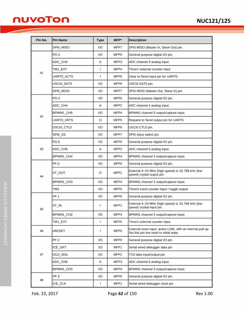
NUC121/125
Feb. 23, 2017 Page 62 of 150 Rev 1.00
NU
C12
1/1
25 S
ER
IES
DA
TA
SH
EE
T
Pin No. Pin Name Type MFP* Description
SPI0_MISO I/O MFP7 SPI0 MISO (Master In, Slave Out) pin.
41
PD.3 I/O MFP0 General purpose digital I/O pin.
ADC_CH3 A MFP3 ADC channel 3 analog input.
TM1_EXT I MFP4 Timer1 external counter input
UART0_nCTS I MFP5 Clear to Send input pin for UART0.
USCI0_DAT0 I/O MFP6 USCI0 DAT0 pin.
SPI0_MOSI I/O MFP7 SPI0 MOSI (Master Out, Slave In) pin.
42
PD.4 I/O MFP0 General purpose digital I/O pin.
ADC_CH4 A MFP2 ADC channel 4 analog input.
BPWM1_CH5 I/O MFP4 BPWM1 channel 5 output/capture input.
UART0_nRTS O MFP5 Request to Send output pin for UART0.
USCI0_CTL0 I/O MFP6 USCI0 CTL0 pin.
SPI0_SS I/O MFP7 SPI0 slave select pin.
43
PD.5 I/O MFP0 General purpose digital I/O pin.
ADC_CH5 A MFP2 ADC channel 5 analog input.
BPWM1_CH4 I/O MFP4 BPWM1 channel 4 output/capture input.
44
PF.0 I/O MFP0 General purpose digital I/O pin.
XT_OUT O MFP1 External 4~24 MHz (high speed) or 32.768 kHz (low speed) crystal output pin.
BPWM1_CH3 I/O MFP4 BPWM1 channel 3 output/capture input.
TM3 I/O MFP5 Timer3 event counter input / toggle output
45
PF.1 I/O MFP0 General purpose digital I/O pin.
XT_IN I MFP1 External 4~24 MHz (high speed) or 32.768 kHz (low speed) crystal input pin.
BPWM1_CH2 I/O MFP4 BPWM1 channel 2 output/capture input.
TM1_EXT I MFP5 Timer1 external counter input
46 nRESET I MFP0 External reset input: active LOW, with an internal pull-up. Set this pin low reset to initial state.
47
PF.2 I/O MFP0 General purpose digital I/O pin.
ICE_DAT I/O MFP1 Serial wired debugger data pin
I2C0_SDA I/O MFP2 I2C0 data input/output pin.
ADC_CH6 A MFP3 ADC channel 6 analog input.
BPWM1_CH3 I/O MFP4 BPWM1 channel 3 output/capture input.
48 PF.3 I/O MFP0 General purpose digital I/O pin.
ICE_CLK I MFP1 Serial wired debugger clock pin
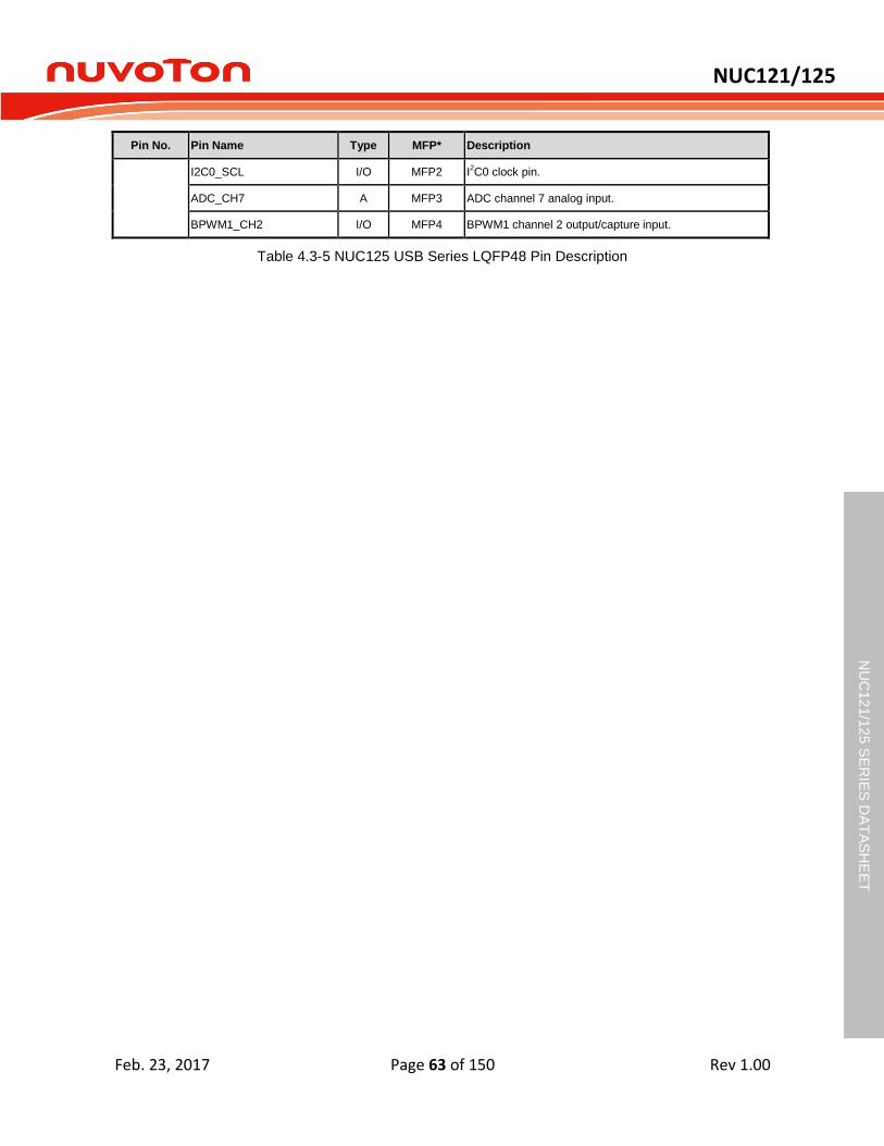
NUC121/125
Feb. 23, 2017 Page 63 of 150 Rev 1.00
NU
C12
1/1
25 S
ER
IES
DA
TA
SH
EE
T
Pin No. Pin Name Type MFP* Description
I2C0_SCL I/O MFP2 I2C0 clock pin.
ADC_CH7 A MFP3 ADC channel 7 analog input.
BPWM1_CH2 I/O MFP4 BPWM1 channel 2 output/capture input.
Table 4.3-5 NUC125 USB Series LQFP48 Pin Description
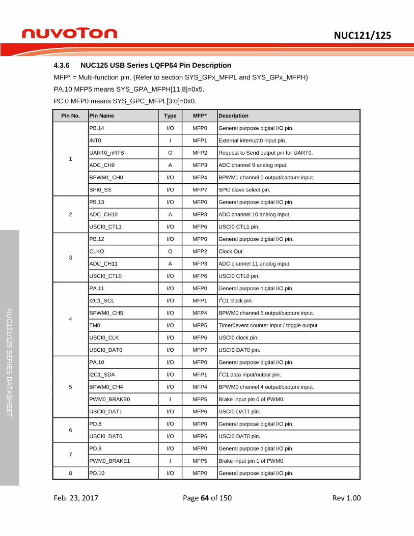
NUC121/125
Feb. 23, 2017 Page 64 of 150 Rev 1.00
NU
C12
1/1
25 S
ER
IES
DA
TA
SH
EE
T
4.3.6 NUC125 USB Series LQFP64 Pin Description
MFP* = Multi-function pin. (Refer to section SYS_GPx_MFPL and SYS_GPx_MFPH)
PA.10 MFP5 means SYS_GPA_MFPH[11:8]=0x5.
PC.0 MFP0 means SYS_GPC_MFPL[3:0]=0x0.
Pin No. Pin Name Type MFP* Description
1
PB.14 I/O MFP0 General purpose digital I/O pin.
INT0 I MFP1 External interrupt0 input pin.
UART0_nRTS O MFP2 Request to Send output pin for UART0.
ADC_CH9 A MFP3 ADC channel 9 analog input.
BPWM1_CH0 I/O MFP4 BPWM1 channel 0 output/capture input.
SPI0_SS I/O MFP7 SPI0 slave select pin.
2
PB.13 I/O MFP0 General purpose digital I/O pin.
ADC_CH10 A MFP3 ADC channel 10 analog input.
USCI0_CTL1 I/O MFP6 USCI0 CTL1 pin.
3
PB.12 I/O MFP0 General purpose digital I/O pin.
CLKO O MFP2 Clock Out
ADC_CH11 A MFP3 ADC channel 11 analog input.
USCI0_CTL0 I/O MFP6 USCI0 CTL0 pin.
4
PA.11 I/O MFP0 General purpose digital I/O pin.
I2C1_SCL I/O MFP1 I2C1 clock pin.
BPWM0_CH5 I/O MFP4 BPWM0 channel 5 output/capture input.
TM0 I/O MFP5 Timer0event counter input / toggle output
USCI0_CLK I/O MFP6 USCI0 clock pin.
USCI0_DAT0 I/O MFP7 USCI0 DAT0 pin.
5
PA.10 I/O MFP0 General purpose digital I/O pin.
I2C1_SDA I/O MFP1 I2C1 data input/output pin.
BPWM0_CH4 I/O MFP4 BPWM0 channel 4 output/capture input.
PWM0_BRAKE0 I MFP5 Brake input pin 0 of PWM0.
USCI0_DAT1 I/O MFP6 USCI0 DAT1 pin.
6 PD.8 I/O MFP0 General purpose digital I/O pin.
USCI0_DAT0 I/O MFP6 USCI0 DAT0 pin.
7 PD.9 I/O MFP0 General purpose digital I/O pin.
PWM0_BRAKE1 I MFP5 Brake input pin 1 of PWM0.
8 PD.10 I/O MFP0 General purpose digital I/O pin.

NUC121/125
Feb. 23, 2017 Page 65 of 150 Rev 1.00
NU
C12
1/1
25 S
ER
IES
DA
TA
SH
EE
T
Pin No. Pin Name Type MFP* Description
CLKO O MFP1 Clock Out
BPWM0_CH5 I/O MFP4 BPWM0 channel 5 output/capture input.
9
PD.11 I/O MFP0 General purpose digital I/O pin.
INT1 I MFP1 External interrupt1 input pin.
BPWM0_CH4 I/O MFP4 BPWM0 channel 4 output/capture input.
10
PB.4 I/O MFP0 General purpose digital I/O pin.
BPWM0_CH3 I/O MFP4 BPWM0 channel 3 output/capture input.
TM2_EXT I MFP5 Timer2 external counter input
USCI0_CTL0 I/O MFP6 USCI0 CTL0 pin.
USCI0_DAT0 I/O MFP7 USCI0 DAT0 pin.
11
PB.5 I/O MFP0 General purpose digital I/O pin.
BPWM0_CH2 I/O MFP4 BPWM0 channel 2 output/capture input.
TM3 I/O MFP5 Timer3 event counter input / toggle output
USCI0_CLK I/O MFP6 USCI0 clock pin.
USCI0_DAT1 I/O MFP7 USCI0 DAT1 pin.
12
PB.6 I/O MFP0 General purpose digital I/O pin.
BPWM0_CH1 I/O MFP4 BPWM0 channel 1 output/capture input.
USCI0_DAT0 I/O MFP6 USCI0 DAT0 pin.
USCI0_CTL1 I/O MFP7 USCI0 CTL1 pin.
13
PB.7 I/O MFP0 General purpose digital I/O pin.
BPWM0_CH0 I/O MFP4 BPWM0 channel 0 output/capture input.
USCI0_DAT1 I/O MFP6 USCI0 DAT1 pin.
USCI0_CTL0 I/O MFP7 USCI0 CTL0 pin.
14 LDO_CAP A MFP0 LDO output pin.
15 VDD A MFP0 Power supply for I/O ports and LDO source for internal PLL and digital function.
16 VSS A MFP0 Ground pin for digital circuit.
17 USB_VBUS A MFP0 Power supply from USB host or HUB.
18 USB_VDD33_CAP A MFP0 Internal power regulator output 3.3V decoupling pin.
19 USB_D- I MFP0 USB differential signal D-.
20 USB_D+ I MFP0 USB differential signal D+.
21
PB.0 I/O MFP0 General purpose digital I/O pin.
UART0_RXD I MFP1 Data receiver input pin for UART0.
PWM1_CH0 I/O MFP4 PWM1 channel0 output/capture input.
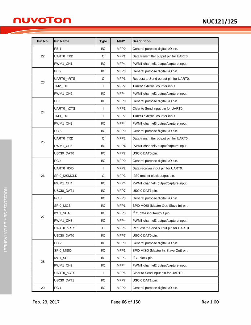
NUC121/125
Feb. 23, 2017 Page 66 of 150 Rev 1.00
NU
C12
1/1
25 S
ER
IES
DA
TA
SH
EE
T
Pin No. Pin Name Type MFP* Description
22
PB.1 I/O MFP0 General purpose digital I/O pin.
UART0_TXD O MFP1 Data transmitter output pin for UART0.
PWM1_CH1 I/O MFP4 PWM1 channel1 output/capture input.
23
PB.2 I/O MFP0 General purpose digital I/O pin.
UART0_nRTS O MFP1 Request to Send output pin for UART0.
TM2_EXT I MFP2 Timer2 external counter input
PWM1_CH2 I/O MFP4 PWM1 channel2 output/capture input.
24
PB.3 I/O MFP0 General purpose digital I/O pin.
UART0_nCTS I MFP1 Clear to Send input pin for UART0.
TM3_EXT I MFP2 Timer3 external counter input
PWM1_CH3 I/O MFP4 PWM1 channel3 output/capture input.
25
PC.5 I/O MFP0 General purpose digital I/O pin.
UART0_TXD O MFP2 Data transmitter output pin for UART0.
PWM1_CH5 I/O MFP4 PWM1 channel5 output/capture input.
USCI0_DAT0 I/O MFP7 USCI0 DAT0 pin.
26
PC.4 I/O MFP0 General purpose digital I/O pin.
UART0_RXD I MFP2 Data receiver input pin for UART0.
SPI0_I2SMCLK O MFP3 I2S0 master clock output pin.
PWM1_CH4 I/O MFP4 PWM1 channel4 output/capture input.
USCI0_DAT1 I/O MFP7 USCI0 DAT1 pin.
27
PC.3 I/O MFP0 General purpose digital I/O pin.
SPI0_MOSI I/O MFP1 SPI0 MOSI (Master Out, Slave In) pin.
I2C1_SDA I/O MFP3 I2C1 data input/output pin.
PWM1_CH3 I/O MFP4 PWM1 channel3 output/capture input.
UART0_nRTS O MFP6 Request to Send output pin for UART0.
USCI0_DAT0 I/O MFP7 USCI0 DAT0 pin.
28
PC.2 I/O MFP0 General purpose digital I/O pin.
SPI0_MISO I/O MFP1 SPI0 MISO (Master In, Slave Out) pin.
I2C1_SCL I/O MFP3 I2C1 clock pin.
PWM1_CH2 I/O MFP4 PWM1 channel2 output/capture input.
UART0_nCTS I MFP6 Clear to Send input pin for UART0.
USCI0_DAT1 I/O MFP7 USCI0 DAT1 pin.
29 PC.1 I/O MFP0 General purpose digital I/O pin.
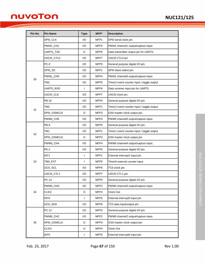
NUC121/125
Feb. 23, 2017 Page 67 of 150 Rev 1.00
NU
C12
1/1
25 S
ER
IES
DA
TA
SH
EE
T
Pin No. Pin Name Type MFP* Description
SPI0_CLK I/O MFP1 SPI0 serial clock pin.
PWM1_CH1 I/O MFP4 PWM1 channel1 output/capture input.
UART0_TXD O MFP6 Data transmitter output pin for UART0.
USCI0_CTL0 I/O MFP7 USCI0 CTL0 pin
30
PC.0 I/O MFP0 General purpose digital I/O pin.
SPI0_SS I/O MFP1 SPI0 slave select pin.
PWM1_CH0 I/O MFP4 PWM1 channel0 output/capture input.
TM2 I/O MFP5 Timer2 event counter input / toggle output
UART0_RXD I MFP6 Data receiver input pin for UART0.
USCI0_CLK I/O MFP7 USCI0 clock pin.
31
PB.10 I/O MFP0 General purpose digital I/O pin.
TM2 I/O MFP1 Timer2 event counter input / toggle output
SPI0_I2SMCLK O MFP3 I2S0 master clock output pin.
PWM0_CH5 I/O MFP4 PWM0 channel5 output/capture input.
32
PB.9 I/O MFP0 General purpose digital I/O pin.
TM1 I/O MFP1 Timer1 event counter input / toggle output
SPI0_I2SMCLK O MFP3 I2S0 master clock output pin.
PWM0_CH4 I/O MFP4 PWM0 channel4 output/capture input.
33
PE.2 I/O MFP0 General purpose digital I/O pin.
INT1 I MFP1 External interrupt1 input pin.
TM0_EXT I MFP5 Timer0 external counter input
I2C0_SCL I/O MFP6 I2C0 clock pin.
USCI0_CTL1 I/O MFP7 USCI0 CTL1 pin.
34
PC.13 I/O MFP0 General purpose digital I/O pin.
PWM0_CH3 I/O MFP2 PWM0 channel3 output/capture input.
CLKO O MFP3 Clock Out
INT0 I MFP5 External interrupt0 input pin.
I2C0_SDA I/O MFP6 I2C0 data input/output pin.
35
PC.12 I/O MFP0 General purpose digital I/O pin.
PWM0_CH2 I/O MFP2 PWM0 channel2 output/capture input.
SPI0_I2SMCLK O MFP3 I2S0 master clock output pin.
CLKO O MFP4 Clock Out
INT0 I MFP5 External interrupt0 input pin.

NUC121/125
Feb. 23, 2017 Page 68 of 150 Rev 1.00
NU
C12
1/1
25 S
ER
IES
DA
TA
SH
EE
T
Pin No. Pin Name Type MFP* Description
I2C0_SCL I/O MFP6 I2C0 clock pin.
USCI0_CTL1 I/O MFP7 USCI0 CTL1 pin.
36
PC.11 I/O MFP0 General purpose digital I/O pin.
SPI0_MOSI I/O MFP3 SPI0 MOSI (Master Out, Slave In) pin.
PWM0_CH1 I/O MFP4 PWM0 channel1 output/capture input.
TM1 I/O MFP5 Timer1 event counter input / toggle output
I2C0_SDA I/O MFP6 I2C0 data input/output pin.
USCI0_DAT0 I/O MFP7 USCI0 DAT0 pin.
37
PC.10 I/O MFP0 General purpose digital I/O pin.
SPI0_MISO I/O MFP3 SPI0 MISO (Master In, Slave Out) pin.
PWM0_CH0 I/O MFP4 PWM0 channel0 output/capture input.
USCI0_DAT1 I/O MFP7 USCI0 DAT1 pin.
38
PE.1 I/O MFP0 General purpose digital I/O pin.
STADC I MFP2 ADC external trigger input.
CLKO O MFP3 Clock Out
TM3 I/O MFP5 Timer3 event counter input / toggle output
USCI0_DAT1 I/O MFP7 USCI0 DAT1 pin.
39
PC.9 I/O MFP0 General purpose digital I/O pin.
SPI0_CLK I/O MFP3 SPI0 serial clock pin.
PWM0_CH5 I/O MFP4 PWM0 channel5 output/capture input.
PWM0_BRAKE1 I MFP5 Brake input pin 1 of PWM0.
USCI0_CLK I/O MFP7 USCI0 clock pin
40
PC.8 I/O MFP0 General purpose digital I/O pin.
STADC I MFP2 ADC external trigger input.
SPI0_SS I/O MFP3 SPI0 slave select pin.
PWM0_CH4 I/O MFP4 PWM0 channel4 output/capture input.
PWM1_BRAKE0 I MFP5 Brake input pin 0 of PWM1.
USCI0_CTL0 I/O MFP7 USCI0 CTL0 pin
41
PA.15 I/O MFP0 General purpose digital I/O pin.
PWM0_CH3 I/O MFP1 PWM0 channel3 output/capture input.
SPI_I2SMCLK O MFP2 I2S0 master clock output pin.
CLKO O MFP3 Clock Out
PWM1_BRAKE1 I MFP4 Brake input pin 1 of PWM1.
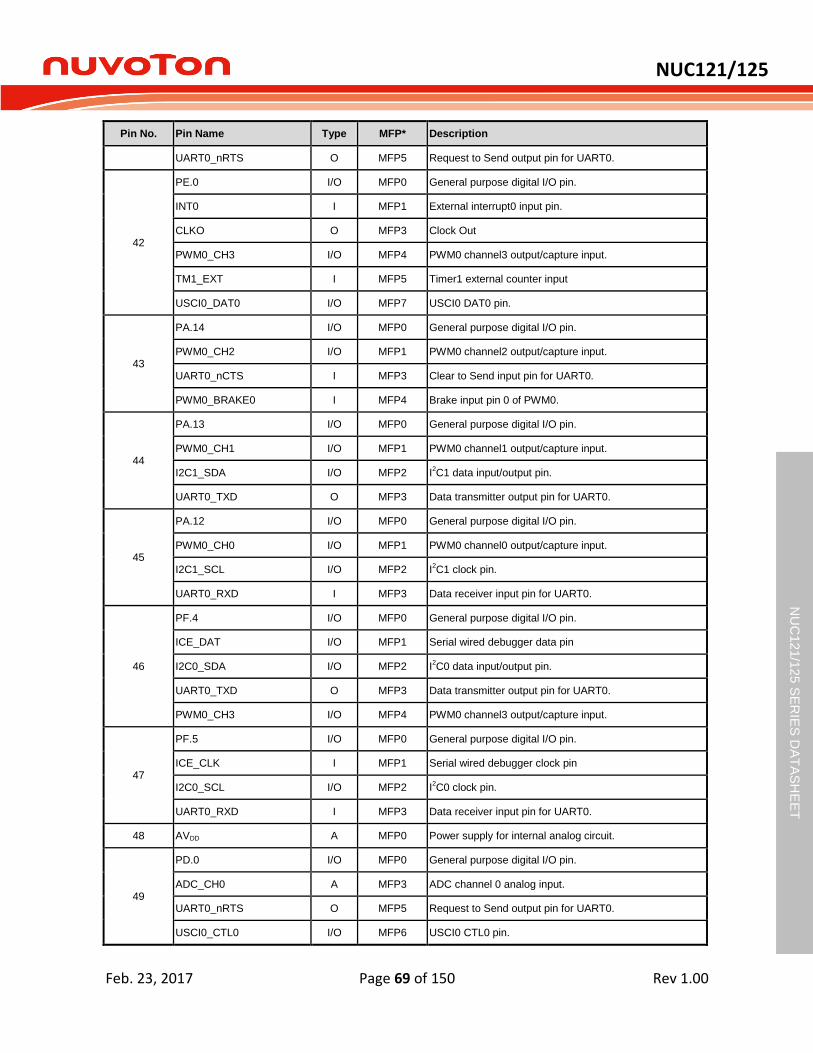
NUC121/125
Feb. 23, 2017 Page 69 of 150 Rev 1.00
NU
C12
1/1
25 S
ER
IES
DA
TA
SH
EE
T
Pin No. Pin Name Type MFP* Description
UART0_nRTS O MFP5 Request to Send output pin for UART0.
42
PE.0 I/O MFP0 General purpose digital I/O pin.
INT0 I MFP1 External interrupt0 input pin.
CLKO O MFP3 Clock Out
PWM0_CH3 I/O MFP4 PWM0 channel3 output/capture input.
TM1_EXT I MFP5 Timer1 external counter input
USCI0_DAT0 I/O MFP7 USCI0 DAT0 pin.
43
PA.14 I/O MFP0 General purpose digital I/O pin.
PWM0_CH2 I/O MFP1 PWM0 channel2 output/capture input.
UART0_nCTS I MFP3 Clear to Send input pin for UART0.
PWM0_BRAKE0 I MFP4 Brake input pin 0 of PWM0.
44
PA.13 I/O MFP0 General purpose digital I/O pin.
PWM0_CH1 I/O MFP1 PWM0 channel1 output/capture input.
I2C1_SDA I/O MFP2 I2C1 data input/output pin.
UART0_TXD O MFP3 Data transmitter output pin for UART0.
45
PA.12 I/O MFP0 General purpose digital I/O pin.
PWM0_CH0 I/O MFP1 PWM0 channel0 output/capture input.
I2C1_SCL I/O MFP2 I2C1 clock pin.
UART0_RXD I MFP3 Data receiver input pin for UART0.
46
PF.4 I/O MFP0 General purpose digital I/O pin.
ICE_DAT I/O MFP1 Serial wired debugger data pin
I2C0_SDA I/O MFP2 I2C0 data input/output pin.
UART0_TXD O MFP3 Data transmitter output pin for UART0.
PWM0_CH3 I/O MFP4 PWM0 channel3 output/capture input.
47
PF.5 I/O MFP0 General purpose digital I/O pin.
ICE_CLK I MFP1 Serial wired debugger clock pin
I2C0_SCL I/O MFP2 I2C0 clock pin.
UART0_RXD I MFP3 Data receiver input pin for UART0.
48 AVDD A MFP0 Power supply for internal analog circuit.
49
PD.0 I/O MFP0 General purpose digital I/O pin.
ADC_CH0 A MFP3 ADC channel 0 analog input.
UART0_nRTS O MFP5 Request to Send output pin for UART0.
USCI0_CTL0 I/O MFP6 USCI0 CTL0 pin.
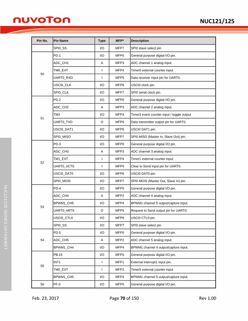
NUC121/125
Feb. 23, 2017 Page 70 of 150 Rev 1.00
NU
C12
1/1
25 S
ER
IES
DA
TA
SH
EE
T
Pin No. Pin Name Type MFP* Description
SPI0_SS I/O MFP7 SPI0 slave select pin.
50
PD.1 I/O MFP0 General purpose digital I/O pin.
ADC_CH1 A MFP3 ADC channel 1 analog input.
TM0_EXT I MFP4 Timer0 external counter input
UART0_RXD I MFP5 Data receiver input pin for UART0.
USCI0_CLK I/O MFP6 USCI0 clock pin.
SPI0_CLK I/O MFP7 SPI0 serial clock pin.
51
PD.2 I/O MFP0 General purpose digital I/O pin.
ADC_CH2 A MFP3 ADC channel 2 analog input.
TM3 I/O MFP4 Timer3 event counter input / toggle output
UART0_TXD O MFP5 Data transmitter output pin for UART0.
USCI0_DAT1 I/O MFP6 USCI0 DAT1 pin.
SPI0_MISO I/O MFP7 SPI0 MISO (Master In, Slave Out) pin.
52
PD.3 I/O MFP0 General purpose digital I/O pin.
ADC_CH3 A MFP3 ADC channel 3 analog input.
TM1_EXT I MFP4 Timer1 external counter input
UART0_nCTS I MFP5 Clear to Send input pin for UART0.
USCI0_DAT0 I/O MFP6 USCI0 DAT0 pin.
SPI0_MOSI I/O MFP7 SPI0 MOSI (Master Out, Slave In) pin.
53
PD.4 I/O MFP0 General purpose digital I/O pin.
ADC_CH4 A MFP2 ADC channel 4 analog input.
BPWM1_CH5 I/O MFP4 BPWM1 channel 5 output/capture input.
UART0_nRTS O MFP5 Request to Send output pin for UART0.
USCI0_CTL0 I/O MFP6 USCI0 CTL0 pin.
SPI0_SS I/O MFP7 SPI0 slave select pin.
54
PD.5 I/O MFP0 General purpose digital I/O pin.
ADC_CH5 A MFP2 ADC channel 5 analog input.
BPWM1_CH4 I/O MFP4 BPWM1 channel 4 output/capture input.
55
PB.15 I/O MFP0 General purpose digital I/O pin.
INT1 I MFP1 External interrupt1 input pin.
TM0_EXT I MFP2 Timer0 external counter input
BPWM1_CH5 I/O MFP4 BPWM1 channel 5 output/capture input.
56 PF.0 I/O MFP0 General purpose digital I/O pin.
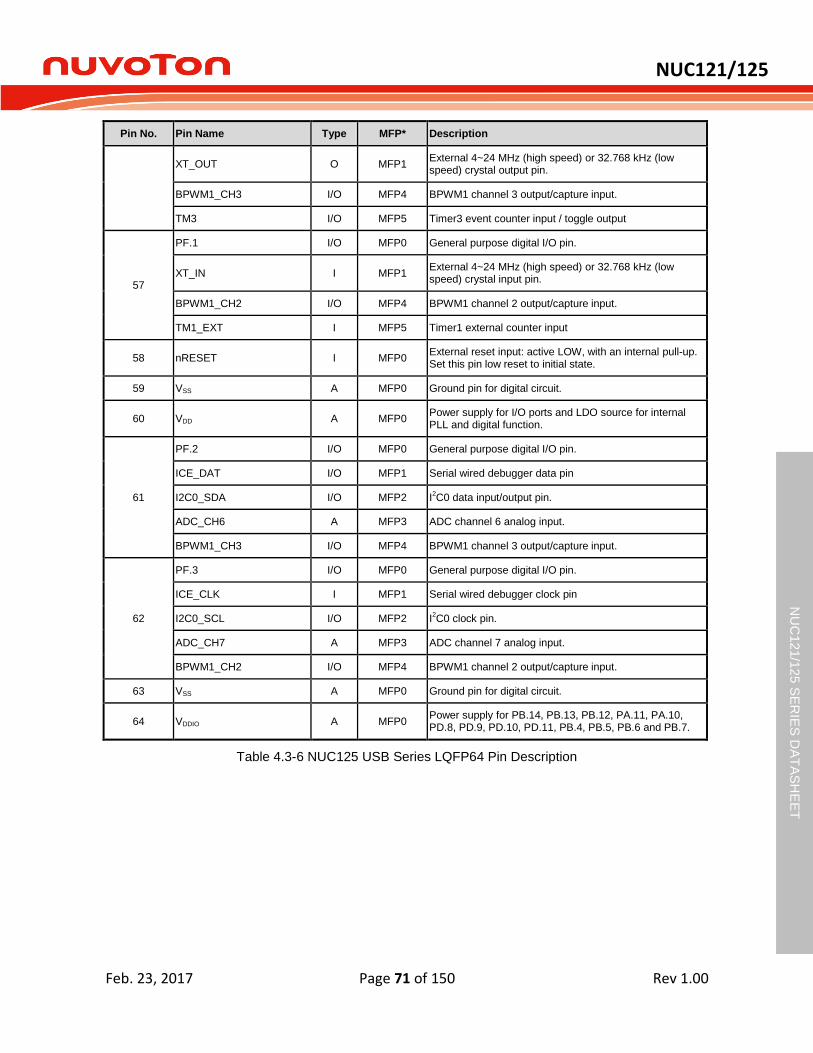
NUC121/125
Feb. 23, 2017 Page 71 of 150 Rev 1.00
NU
C12
1/1
25 S
ER
IES
DA
TA
SH
EE
T
Pin No. Pin Name Type MFP* Description
XT_OUT O MFP1 External 4~24 MHz (high speed) or 32.768 kHz (low speed) crystal output pin.
BPWM1_CH3 I/O MFP4 BPWM1 channel 3 output/capture input.
TM3 I/O MFP5 Timer3 event counter input / toggle output
57
PF.1 I/O MFP0 General purpose digital I/O pin.
XT_IN I MFP1 External 4~24 MHz (high speed) or 32.768 kHz (low speed) crystal input pin.
BPWM1_CH2 I/O MFP4 BPWM1 channel 2 output/capture input.
TM1_EXT I MFP5 Timer1 external counter input
58 nRESET I MFP0 External reset input: active LOW, with an internal pull-up. Set this pin low reset to initial state.
59 VSS A MFP0 Ground pin for digital circuit.
60 VDD A MFP0 Power supply for I/O ports and LDO source for internal PLL and digital function.
61
PF.2 I/O MFP0 General purpose digital I/O pin.
ICE_DAT I/O MFP1 Serial wired debugger data pin
I2C0_SDA I/O MFP2 I2C0 data input/output pin.
ADC_CH6 A MFP3 ADC channel 6 analog input.
BPWM1_CH3 I/O MFP4 BPWM1 channel 3 output/capture input.
62
PF.3 I/O MFP0 General purpose digital I/O pin.
ICE_CLK I MFP1 Serial wired debugger clock pin
I2C0_SCL I/O MFP2 I2C0 clock pin.
ADC_CH7 A MFP3 ADC channel 7 analog input.
BPWM1_CH2 I/O MFP4 BPWM1 channel 2 output/capture input.
63 VSS A MFP0 Ground pin for digital circuit.
64 VDDIO A MFP0 Power supply for PB.14, PB.13, PB.12, PA.11, PA.10, PD.8, PD.9, PD.10, PD.11, PB.4, PB.5, PB.6 and PB.7.
Table 4.3-6 NUC125 USB Series LQFP64 Pin Description
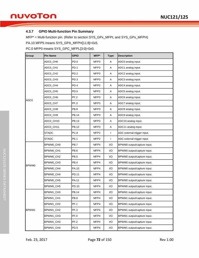
NUC121/125
Feb. 23, 2017 Page 72 of 150 Rev 1.00
NU
C12
1/1
25 S
ER
IES
DA
TA
SH
EE
T
4.3.7 GPIO Multi-function Pin Summary
MFP* = Multi-function pin. (Refer to section SYS_GPx_MFPL and SYS_GPx_MFPH)
PA.10 MFP5 means SYS_GPA_MFPH[11:8]=0x5.
PC.0 MFP0 means SYS_GPC_MFPL[3:0]=0x0.
Group Pin Name GPIO MFP* Type Description
ADC0
ADC0_CH0 PD.0 MFP3 A ADC0 analog input.
ADC0_CH1 PD.1 MFP3 A ADC1 analog input.
ADC0_CH2 PD.2 MFP3 A ADC2 analog input.
ADC0_CH3 PD.3 MFP3 A ADC3 analog input.
ADC0_CH4 PD.4 MFP2 A ADC4 analog input.
ADC0_CH5 PD.5 MFP2 A ADC5 analog input.
ADC0_CH6 PF.2 MFP3 A ADC6 analog input.
ADC0_CH7 PF.3 MFP3 A ADC7 analog input.
ADC0_CH8 PB.8 MFP3 A ADC8 analog input.
ADC0_CH9 PB.14 MFP3 A ADC9 analog input.
ADC0_CH10 PB.13 MFP3 A ADC10 analog input.
ADC0_CH11 PB.12 MFP3 A ADC11 analog input.
STADC PC.8 MFP2 I ADC external trigger input.
STADC PE.1 MFP2 I ADC external trigger input
BPWM0
BPWM0_CH0 PB.7 MFP4 I/O BPWM0 output/capture input.
BPWM0_CH1 PB.6 MFP4 I/O BPWM0 output/capture input.
BPWM0_CH2 PB.5 MFP4 I/O BPWM0 output/capture input.
BPWM0_CH3 PB.4 MFP4 I/O BPWM0 output/capture input.
BPWM0_CH4 PA.10 MFP4 I/O BPWM0 output/capture input.
BPWM0_CH4 PD.11 MFP4 I/O BPWM0 output/capture input.
BPWM0_CH5 PA.11 MFP4 I/O BPWM0 output/capture input.
BPWM0_CH5 PD.10 MFP4 I/O BPWM0 output/capture input.
BPWM1
BPWM1_CH0 PB.14 MFP4 I/O BPWM1 output/capture input.
BPWM1_CH1 PB.8 MFP4 I/O BPWM1 output/capture input.
BPWM1_CH2 PF.1 MFP4 I/O BPWM1 output/capture input.
BPWM1_CH2 PF.3 MFP4 I/O BPWM1 output/capture input.
BPWM1_CH3 PF.0 MFP4 I/O BPWM1 output/capture input.
BPWM1_CH3 PF.2 MFP4 I/O BPWM1 output/capture input.
BPWM1_CH4 PD.5 MFP4 I/O BPWM1 output/capture input.
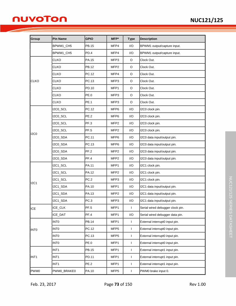
NUC121/125
Feb. 23, 2017 Page 73 of 150 Rev 1.00
NU
C12
1/1
25 S
ER
IES
DA
TA
SH
EE
T
Group Pin Name GPIO MFP* Type Description
BPWM1_CH5 PB.15 MFP4 I/O BPWM1 output/capture input.
BPWM1_CH5 PD.4 MFP4 I/O BPWM1 output/capture input.
CLKO
CLKO PA.15 MFP3 O Clock Out.
CLKO PB.12 MFP2 O Clock Out.
CLKO PC.12 MFP4 O Clock Out.
CLKO PC.13 MFP3 O Clock Out.
CLKO PD.10 MFP1 O Clock Out.
CLKO PE.0 MFP3 O Clock Out.
CLKO PE.1 MFP3 O Clock Out.
I2C0
I2C0_SCL PC.12 MFP6 I/O I2C0 clock pin.
I2C0_SCL PE.2 MFP6 I/O I2C0 clock pin.
I2C0_SCL PF.3 MFP2 I/O I2C0 clock pin.
I2C0_SCL PF.5 MFP2 I/O I2C0 clock pin.
I2C0_SDA PC.11 MFP6 I/O I2C0 data input/output pin.
I2C0_SDA PC.13 MFP6 I/O I2C0 data input/output pin.
I2C0_SDA PF.2 MFP2 I/O I2C0 data input/output pin.
I2C0_SDA PF.4 MFP2 I/O I2C0 data input/output pin.
I2C1
I2C1_SCL PA.11 MFP1 I/O I2C1 clock pin.
I2C1_SCL PA.12 MFP2 I/O I2C1 clock pin.
I2C1_SCL PC.2 MFP3 I/O I2C1 clock pin.
I2C1_SDA PA.10 MFP1 I/O I2C1 data input/output pin.
I2C1_SDA PA.13 MFP2 I/O I2C1 data input/output pin.
I2C1_SDA PC.3 MFP3 I/O I2C1 data input/output pin.
ICE
ICE_CLK PF.5 MFP1 I Serial wired debugger clock pin.
ICE_DAT PF.4 MFP1 I/O Serial wired debugger data pin.
INT0
INT0 PB.14 MFP1 I External interrupt0 input pin.
INT0 PC.12 MFP5 I External interrupt0 input pin.
INT0 PC.13 MFP5 I External interrupt0 input pin.
INT0 PE.0 MFP1 I External interrupt0 input pin.
INT1
INT1 PB.15 MFP1 I External interrupt1 input pin.
INT1 PD.11 MFP1 I External interrupt1 input pin.
INT1 PE.2 MFP1 I External interrupt1 input pin.
PWM0 PWM0_BRAKE0 PA.10 MFP5 I PWM0 brake input 0.
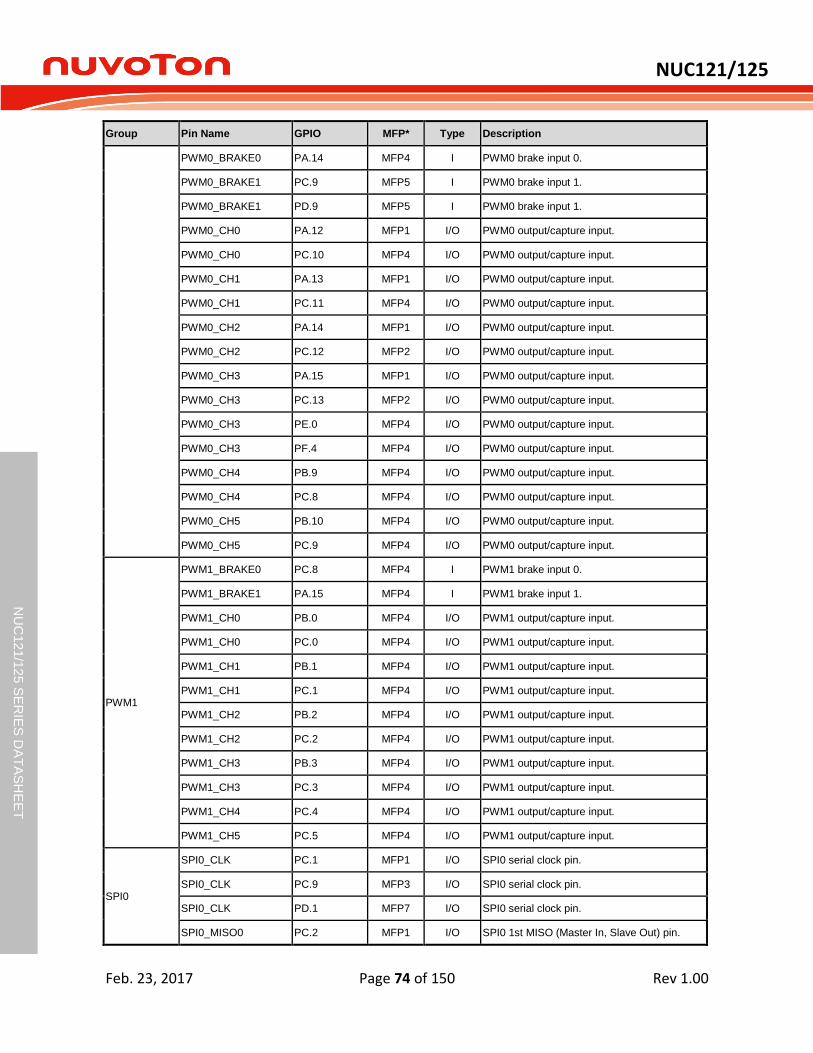
NUC121/125
Feb. 23, 2017 Page 74 of 150 Rev 1.00
NU
C12
1/1
25 S
ER
IES
DA
TA
SH
EE
T
Group Pin Name GPIO MFP* Type Description
PWM0_BRAKE0 PA.14 MFP4 I PWM0 brake input 0.
PWM0_BRAKE1 PC.9 MFP5 I PWM0 brake input 1.
PWM0_BRAKE1 PD.9 MFP5 I PWM0 brake input 1.
PWM0_CH0 PA.12 MFP1 I/O PWM0 output/capture input.
PWM0_CH0 PC.10 MFP4 I/O PWM0 output/capture input.
PWM0_CH1 PA.13 MFP1 I/O PWM0 output/capture input.
PWM0_CH1 PC.11 MFP4 I/O PWM0 output/capture input.
PWM0_CH2 PA.14 MFP1 I/O PWM0 output/capture input.
PWM0_CH2 PC.12 MFP2 I/O PWM0 output/capture input.
PWM0_CH3 PA.15 MFP1 I/O PWM0 output/capture input.
PWM0_CH3 PC.13 MFP2 I/O PWM0 output/capture input.
PWM0_CH3 PE.0 MFP4 I/O PWM0 output/capture input.
PWM0_CH3 PF.4 MFP4 I/O PWM0 output/capture input.
PWM0_CH4 PB.9 MFP4 I/O PWM0 output/capture input.
PWM0_CH4 PC.8 MFP4 I/O PWM0 output/capture input.
PWM0_CH5 PB.10 MFP4 I/O PWM0 output/capture input.
PWM0_CH5 PC.9 MFP4 I/O PWM0 output/capture input.
PWM1
PWM1_BRAKE0 PC.8 MFP4 I PWM1 brake input 0.
PWM1_BRAKE1 PA.15 MFP4 I PWM1 brake input 1.
PWM1_CH0 PB.0 MFP4 I/O PWM1 output/capture input.
PWM1_CH0 PC.0 MFP4 I/O PWM1 output/capture input.
PWM1_CH1 PB.1 MFP4 I/O PWM1 output/capture input.
PWM1_CH1 PC.1 MFP4 I/O PWM1 output/capture input.
PWM1_CH2 PB.2 MFP4 I/O PWM1 output/capture input.
PWM1_CH2 PC.2 MFP4 I/O PWM1 output/capture input.
PWM1_CH3 PB.3 MFP4 I/O PWM1 output/capture input.
PWM1_CH3 PC.3 MFP4 I/O PWM1 output/capture input.
PWM1_CH4 PC.4 MFP4 I/O PWM1 output/capture input.
PWM1_CH5 PC.5 MFP4 I/O PWM1 output/capture input.
SPI0
SPI0_CLK PC.1 MFP1 I/O SPI0 serial clock pin.
SPI0_CLK PC.9 MFP3 I/O SPI0 serial clock pin.
SPI0_CLK PD.1 MFP7 I/O SPI0 serial clock pin.
SPI0_MISO0 PC.2 MFP1 I/O SPI0 1st MISO (Master In, Slave Out) pin.
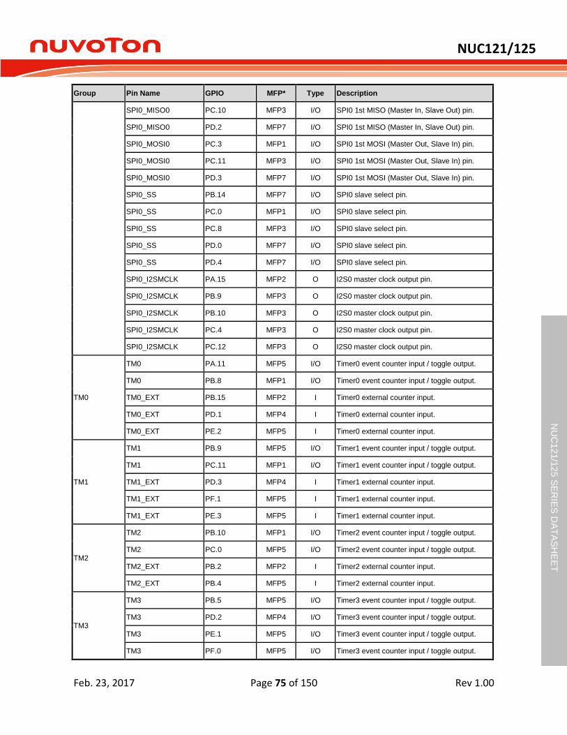
NUC121/125
Feb. 23, 2017 Page 75 of 150 Rev 1.00
NU
C12
1/1
25 S
ER
IES
DA
TA
SH
EE
T
Group Pin Name GPIO MFP* Type Description
SPI0_MISO0 PC.10 MFP3 I/O SPI0 1st MISO (Master In, Slave Out) pin.
SPI0_MISO0 PD.2 MFP7 I/O SPI0 1st MISO (Master In, Slave Out) pin.
SPI0_MOSI0 PC.3 MFP1 I/O SPI0 1st MOSI (Master Out, Slave In) pin.
SPI0_MOSI0 PC.11 MFP3 I/O SPI0 1st MOSI (Master Out, Slave In) pin.
SPI0_MOSI0 PD.3 MFP7 I/O SPI0 1st MOSI (Master Out, Slave In) pin.
SPI0_SS PB.14 MFP7 I/O SPI0 slave select pin.
SPI0_SS PC.0 MFP1 I/O SPI0 slave select pin.
SPI0_SS PC.8 MFP3 I/O SPI0 slave select pin.
SPI0_SS PD.0 MFP7 I/O SPI0 slave select pin.
SPI0_SS PD.4 MFP7 I/O SPI0 slave select pin.
SPI0_I2SMCLK PA.15 MFP2 O I2S0 master clock output pin.
SPI0_I2SMCLK PB.9 MFP3 O I2S0 master clock output pin.
SPI0_I2SMCLK PB.10 MFP3 O I2S0 master clock output pin.
SPI0_I2SMCLK PC.4 MFP3 O I2S0 master clock output pin.
SPI0_I2SMCLK PC.12 MFP3 O I2S0 master clock output pin.
TM0
TM0 PA.11 MFP5 I/O Timer0 event counter input / toggle output.
TM0 PB.8 MFP1 I/O Timer0 event counter input / toggle output.
TM0_EXT PB.15 MFP2 I Timer0 external counter input.
TM0_EXT PD.1 MFP4 I Timer0 external counter input.
TM0_EXT PE.2 MFP5 I Timer0 external counter input.
TM1
TM1 PB.9 MFP5 I/O Timer1 event counter input / toggle output.
TM1 PC.11 MFP1 I/O Timer1 event counter input / toggle output.
TM1_EXT PD.3 MFP4 I Timer1 external counter input.
TM1_EXT PF.1 MFP5 I Timer1 external counter input.
TM1_EXT PE.3 MFP5 I Timer1 external counter input.
TM2
TM2 PB.10 MFP1 I/O Timer2 event counter input / toggle output.
TM2 PC.0 MFP5 I/O Timer2 event counter input / toggle output.
TM2_EXT PB.2 MFP2 I Timer2 external counter input.
TM2_EXT PB.4 MFP5 I Timer2 external counter input.
TM3
TM3 PB.5 MFP5 I/O Timer3 event counter input / toggle output.
TM3 PD.2 MFP4 I/O Timer3 event counter input / toggle output.
TM3 PE.1 MFP5 I/O Timer3 event counter input / toggle output.
TM3 PF.0 MFP5 I/O Timer3 event counter input / toggle output.
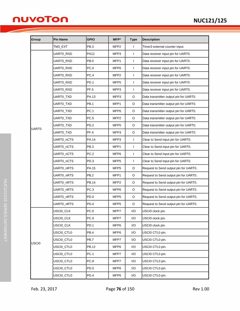
NUC121/125
Feb. 23, 2017 Page 76 of 150 Rev 1.00
NU
C12
1/1
25 S
ER
IES
DA
TA
SH
EE
T
Group Pin Name GPIO MFP* Type Description
TM3_EXT PB.3 MFP2 I Timer3 external counter input.
UART0
UART0_RXD PA12 MFP3 I Data receiver input pin for UART0.
UART0_RXD PB.0 MFP1 I Data receiver input pin for UART0.
UART0_RXD PC.0 MFP6 I Data receiver input pin for UART0.
UART0_RXD PC.4 MFP2 I Data receiver input pin for UART0.
UART0_RXD PD.1 MFP5 I Data receiver input pin for UART0.
UART0_RXD PF.5 MFP3 I Data receiver input pin for UART0.
UART0_TXD PA.13 MFP3 O Data transmitter output pin for UART0.
UART0_TXD PB.1 MFP1 O Data transmitter output pin for UART0.
UART0_TXD PC.1 MFP6 O Data transmitter output pin for UART0.
UART0_TXD PC.5 MFP2 O Data transmitter output pin for UART0.
UART0_TXD PD.2 MFP5 O Data transmitter output pin for UART0.
UART0_TXD PF.4 MFP3 O Data transmitter output pin for UART0.
UART0_nCTS PA.14 MFP3 I Clear to Send input pin for UART0.
UART0_nCTS PB.3 MFP1 I Clear to Send input pin for UART0.
UART0_nCTS PC.2 MFP6 I Clear to Send input pin for UART0.
UART0_nCTS PD.3 MFP5 I Clear to Send input pin for UART0.
UART0_nRTS PA.15 MFP5 O Request to Send output pin for UART0.
UART0_nRTS PB.2 MFP1 O Request to Send output pin for UART0.
UART0_nRTS PB.14 MFP2 O Request to Send output pin for UART0.
UART0_nRTS PC.3 MFP6 O Request to Send output pin for UART0.
UART0_nRTS PD.0 MFP5 O Request to Send output pin for UART0.
UART0_nRTS PD.4 MFP5 O Request to Send output pin for UART0.
USCI0
USCI0_CLK PC.0 MFP7 I/O USCI0 clock pin.
USCI0_CLK PC.9 MFP7 I/O USCI0 clock pin.
USCI0_CLK PD.1 MFP6 I/O USCI0 clock pin.
USCI0_CTL0 PB.4 MFP6 I/O USCI0 CTL0 pin.
USCI0_CTL0 PB.7 MFP7 I/O USCI0 CTL0 pin.
USCI0_CTL0 PB.12 MFP6 I/O USCI0 CTL0 pin.
USCI0_CTL0 PC.1 MFP7 I/O USCI0 CTL0 pin.
USCI0_CTL0 PC.8 MFP7 I/O USCI0 CTL0 pin.
USCI0_CTL0 PD.0 MFP6 I/O USCI0 CTL0 pin.
USCI0_CTL0 PD.4 MFP6 I/O USCI0 CTL0 pin.
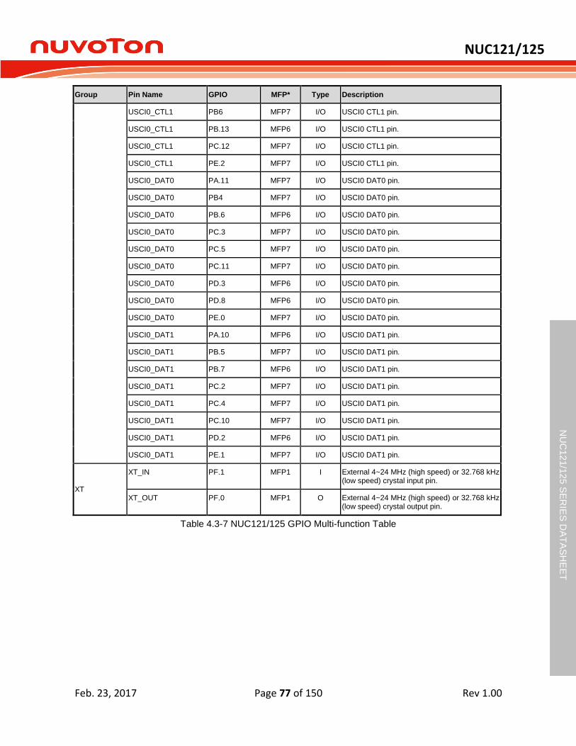
NUC121/125
Feb. 23, 2017 Page 77 of 150 Rev 1.00
NU
C12
1/1
25 S
ER
IES
DA
TA
SH
EE
T
Group Pin Name GPIO MFP* Type Description
USCI0_CTL1 PB6 MFP7 I/O USCI0 CTL1 pin.
USCI0_CTL1 PB.13 MFP6 I/O USCI0 CTL1 pin.
USCI0_CTL1 PC.12 MFP7 I/O USCI0 CTL1 pin.
USCI0_CTL1 PE.2 MFP7 I/O USCI0 CTL1 pin.
USCI0_DAT0 PA.11 MFP7 I/O USCI0 DAT0 pin.
USCI0_DAT0 PB4 MFP7 I/O USCI0 DAT0 pin.
USCI0_DAT0 PB.6 MFP6 I/O USCI0 DAT0 pin.
USCI0_DAT0 PC.3 MFP7 I/O USCI0 DAT0 pin.
USCI0_DAT0 PC.5 MFP7 I/O USCI0 DAT0 pin.
USCI0_DAT0 PC.11 MFP7 I/O USCI0 DAT0 pin.
USCI0_DAT0 PD.3 MFP6 I/O USCI0 DAT0 pin.
USCI0_DAT0 PD.8 MFP6 I/O USCI0 DAT0 pin.
USCI0_DAT0 PE.0 MFP7 I/O USCI0 DAT0 pin.
USCI0_DAT1 PA.10 MFP6 I/O USCI0 DAT1 pin.
USCI0_DAT1 PB.5 MFP7 I/O USCI0 DAT1 pin.
USCI0_DAT1 PB.7 MFP6 I/O USCI0 DAT1 pin.
USCI0_DAT1 PC.2 MFP7 I/O USCI0 DAT1 pin.
USCI0_DAT1 PC.4 MFP7 I/O USCI0 DAT1 pin.
USCI0_DAT1 PC.10 MFP7 I/O USCI0 DAT1 pin.
USCI0_DAT1 PD.2 MFP6 I/O USCI0 DAT1 pin.
USCI0_DAT1 PE.1 MFP7 I/O USCI0 DAT1 pin.
XT
XT_IN PF.1 MFP1 I External 4~24 MHz (high speed) or 32.768 kHz (low speed) crystal input pin.
XT_OUT PF.0 MFP1 O External 4~24 MHz (high speed) or 32.768 kHz (low speed) crystal output pin.
Table 4.3-7 NUC121/125 GPIO Multi-function Table
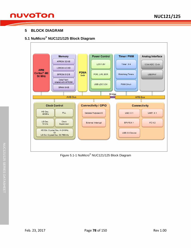
NUC121/125
Feb. 23, 2017 Page 78 of 150 Rev 1.00
NU
C12
1/1
25 S
ER
IES
DA
TA
SH
EE
T
5 BLOCK DIAGRAM
NuMicro® NUC121/125 Block Diagram 5.1
Figure 5.1-1 NuMicro® NUC121/125 Block Diagram
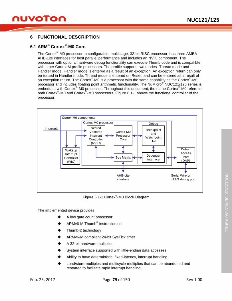
NUC121/125
Feb. 23, 2017 Page 79 of 150 Rev 1.00
NU
C12
1/1
25 S
ER
IES
DA
TA
SH
EE
T
6 FUNCTIONAL DESCRIPTION
ARM® Cortex
®-M0 Core 6.1
The Cortex®-M0 processor, a configurable, multistage, 32-bit RISC processor, has three AMBA
AHB-Lite interfaces for best parallel performance and includes an NVIC component. The processor with optional hardware debug functionality can execute Thumb code and is compatible with other Cortex-M profile processors. The profile supports two modes -Thread mode and Handler mode. Handler mode is entered as a result of an exception. An exception return can only be issued in Handler mode. Thread mode is entered on Reset, and can be entered as a result of an exception return. The Cortex
®-M0 is a processor with the same capability as the Cortex
®-M0
processor and includes floating point arithmetic functionality. The NuMicro® NUC121/125 series is
embedded with Cortex®-M0 processor. Throughout this document, the name Cortex
®-M0 refers to
both Cortex®-M0 and Cortex
®-M0 processors. Figure 6.1-1 shows the functional controller of the
processor.
Cortex-M0
Processor
Core
Nested
Vectored
Interrupt
Controller
(NVIC)
Breakpoint
and
Watchpoint
Unit
Debugger
interfaceBus Matrix
Debug
Access
Port
(DAP)
DebugCortex-M0 processor
Cortex-M0 components
Wakeup
Interrupt
Controller
(WIC)
Interrupts
Serial Wire or
JTAG debug port
AHB-Lite
interface
Figure 6.1-1 Cortex®-M0 Block Diagram
The implemented device provides:
A low gate count processor:
ARMv6-M Thumb® instruction set
Thumb-2 technology
ARMv6-M compliant 24-bit SysTick timer
A 32-bit hardware multiplier
System interface supported with little-endian data accesses
Ability to have deterministic, fixed-latency, interrupt handling
Load/store-multiples and multicycle-multiplies that can be abandoned and restarted to facilitate rapid interrupt handling
NUC121/125
Feb. 23, 2017 Page 80 of 150 Rev 1.00
NU
C12
1/1
25 S
ER
IES
DA
TA
SH
EE
T
C Application Binary Interface compliant exception model. This is the ARMv6-M, C Application Binary Interface (C-ABI) compliant exception model that enables the use of pure C functions as interrupt handlers
Low Power Sleep mode entry using the Wait For Interrupt (WFI), Wait For Event (WFE) instructions, or return from interrupt sleep-on-exit feature
NVIC:
32 external interrupt inputs, each with four levels of priority
Dedicated Non-maskable Interrupt (NMI) input
Supports for both level-sensitive and pulse-sensitive interrupt lines
Supports Wake-up Interrupt Controller (WIC) and, providing Ultra-low Power Sleep mode
Debug Support:
Four hardware breakpoints
Two watchpoints
Program Counter Sampling Register (PCSR) for non-intrusive code profiling
Single step and vector catch capabilities
Bus interfaces:
Single 32-bit AMBA-3 AHB-Lite system interface that provides simple integration to all system peripherals and memory
Single 32-bit slave port that supports the DAP (Debug Access Port)
NUC121/125
Feb. 23, 2017 Page 81 of 150 Rev 1.00
NU
C12
1/1
25 S
ER
IES
DA
TA
SH
EE
T
System Manager 6.2
6.2.1 Overview
The system manager provides the functions of system control, power modes, wake-up sources, reset sources, system memory map, product ID and multi-function pin control. The following sections describe the functions for
System Reset
Power Modes and Wake-up Sources
System Power Distribution
SRAM Memory Orginization
System Control Register for Part Number ID, Chip Reset and Multi-function Pin Control
System Timer (SysTick)
Nested Vectored Interrupt Controller (NVIC)
System Control register
6.2.2 System Reset
The system reset can be issued by one of the events listed below. These reset event flags can be read from SYS_RSTSTS register to determine the reset source. Hardware reset can reset chip through peripheral reset signals. Software reset can trigger reset through control registers.
Hardware Reset Sources
– Power-on Reset (POR) – Low level on the nRESET pin – Watchdog Time-out Reset and Window Watchdog Reset (WDT/WWDT Reset) – Low Voltage Reset (LVR) – Brown-out Detector Reset (BOD Reset) – CPU Lockup Reset
Software Reset Sources
– CHIP Reset will reset whole chip by writing 1 to CHIPRST (SYS_IPRST0[0]) – MCU Reset to reboot but keeping the booting setting from APROM or LDROM by
writing 1 to SYSRESETREQ (AIRCR[2]) – CPU Reset for Cortex® -M0 core Only by writing 1 to CPURST (SYS_IPRST0[1])
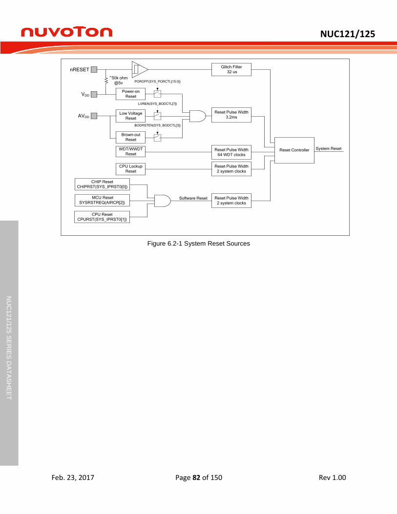
NUC121/125
Feb. 23, 2017 Page 82 of 150 Rev 1.00
NU
C12
1/1
25 S
ER
IES
DA
TA
SH
EE
T
Low Voltage
Reset
Power-on
Reset
Brown-out
Reset
Reset Pulse Width
3.2ms
WDT/WWDT
Reset
System Reset
~50k ohm
@5v
Reset Pulse Width
2 system clocks
nRESET
VDD
AVDD
CHIP Reset
CHIPRST(SYS_IPRST0[0])
CPU Reset
CPURST(SYS_IPRST0[1])
CPU Lockup
Reset
MCU Reset
SYSRSTREQ(AIRCR[2])
LVREN(SYS_BODCTL[7])
BODRSTEN(SYS_BODCTL[3])
POROFF(SYS_PORCTL[15:0])
Reset Pulse Width
64 WDT clocks
Reset Pulse Width
2 system clocks
Glitch Filter
32 us
Software Reset
Reset Controller
Figure 6.2-1 System Reset Sources
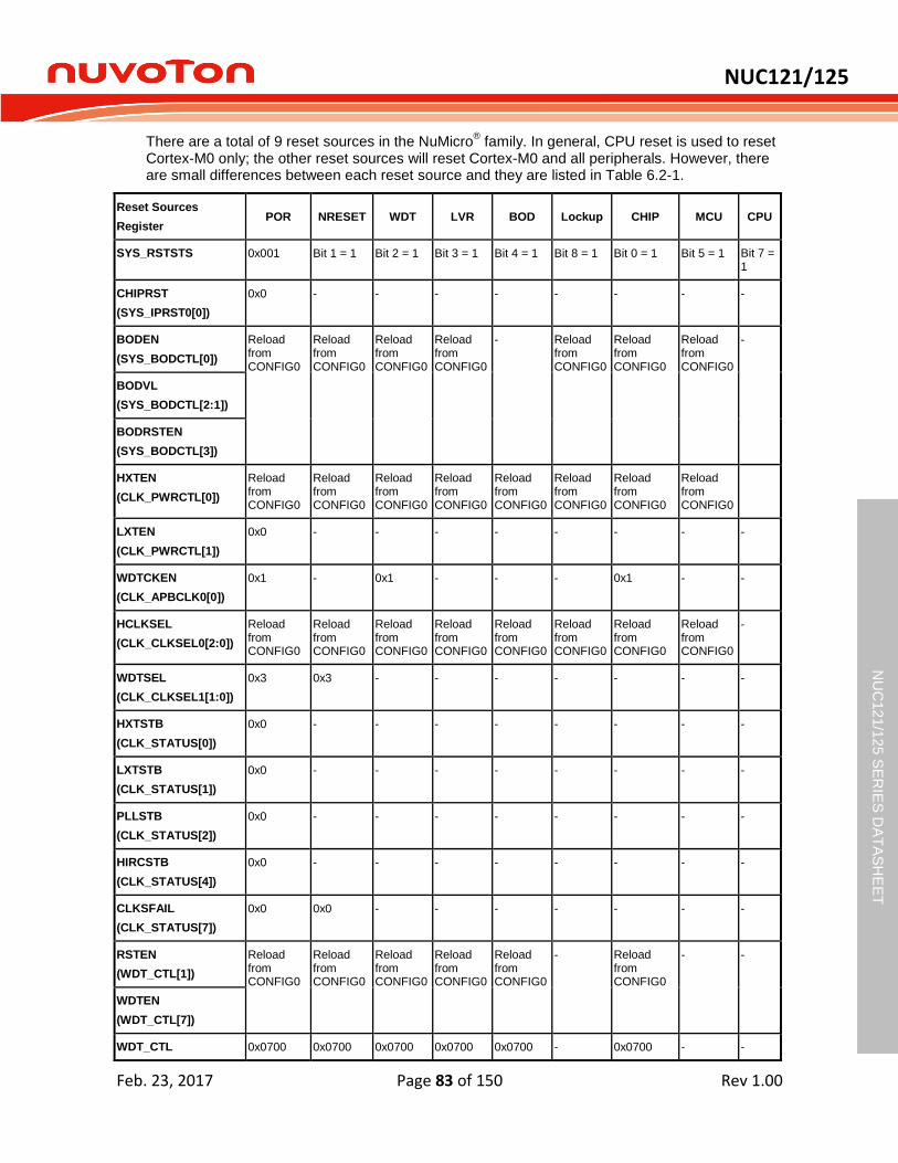
NUC121/125
Feb. 23, 2017 Page 83 of 150 Rev 1.00
NU
C12
1/1
25 S
ER
IES
DA
TA
SH
EE
T
There are a total of 9 reset sources in the NuMicro® family. In general, CPU reset is used to reset
Cortex-M0 only; the other reset sources will reset Cortex-M0 and all peripherals. However, there are small differences between each reset source and they are listed in Table 6.2-1.
Reset Sources
Register POR NRESET WDT LVR BOD Lockup CHIP MCU CPU
SYS_RSTSTS 0x001 Bit 1 = 1 Bit 2 = 1 Bit 3 = 1 Bit 4 = 1 Bit 8 = 1 Bit 0 = 1 Bit 5 = 1 Bit 7 = 1
CHIPRST
(SYS_IPRST0[0])
0x0 - - - - - - - -
BODEN
(SYS_BODCTL[0])
Reload from CONFIG0
Reload from CONFIG0
Reload from CONFIG0
Reload from CONFIG0
- Reload from CONFIG0
Reload from CONFIG0
Reload from CONFIG0
-
BODVL
(SYS_BODCTL[2:1])
BODRSTEN
(SYS_BODCTL[3])
HXTEN
(CLK_PWRCTL[0])
Reload from CONFIG0
Reload from CONFIG0
Reload from CONFIG0
Reload from CONFIG0
Reload from CONFIG0
Reload from CONFIG0
Reload from CONFIG0
Reload from CONFIG0
LXTEN
(CLK_PWRCTL[1])
0x0 - - - - - - - -
WDTCKEN
(CLK_APBCLK0[0])
0x1 - 0x1 - - - 0x1 - -
HCLKSEL
(CLK_CLKSEL0[2:0])
Reload from CONFIG0
Reload from CONFIG0
Reload from CONFIG0
Reload from CONFIG0
Reload from CONFIG0
Reload from CONFIG0
Reload from CONFIG0
Reload from CONFIG0
-
WDTSEL
(CLK_CLKSEL1[1:0])
0x3 0x3 - - - - - - -
HXTSTB
(CLK_STATUS[0])
0x0 - - - - - - - -
LXTSTB
(CLK_STATUS[1])
0x0 - - - - - - - -
PLLSTB
(CLK_STATUS[2])
0x0 - - - - - - - -
HIRCSTB
(CLK_STATUS[4])
0x0 - - - - - - - -
CLKSFAIL
(CLK_STATUS[7])
0x0 0x0 - - - - - - -
RSTEN
(WDT_CTL[1])
Reload from CONFIG0
Reload from CONFIG0
Reload from CONFIG0
Reload from CONFIG0
Reload from CONFIG0
- Reload from CONFIG0
- -
WDTEN
(WDT_CTL[7])
WDT_CTL 0x0700 0x0700 0x0700 0x0700 0x0700 - 0x0700 - -
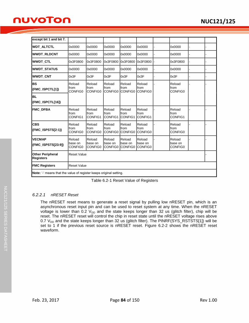
NUC121/125
Feb. 23, 2017 Page 84 of 150 Rev 1.00
NU
C12
1/1
25 S
ER
IES
DA
TA
SH
EE
T
except bit 1 and bit 7.
WDT_ALTCTL 0x0000 0x0000 0x0000 0x0000 0x0000 - 0x0000 - -
WWDT_RLDCNT 0x0000 0x0000 0x0000 0x0000 0x0000 - 0x0000 - -
WWDT_CTL 0x3F0800 0x3F0800 0x3F0800 0x3F0800 0x3F0800 - 0x3F0800 - -
WWDT_STATUS 0x0000 0x0000 0x0000 0x0000 0x0000 - 0x0000 - -
WWDT_CNT 0x3F 0x3F 0x3F 0x3F 0x3F - 0x3F - -
BS
(FMC_ISPCTL[1])
Reload from CONFIG0
Reload from CONFIG0
Reload from CONFIG0
Reload from CONFIG0
Reload from CONFIG0
- Reload from CONFIG0
- -
BL
(FMC_ISPCTL[16])
FMC_DFBA Reload from CONFIG1
Reload from CONFIG1
Reload from CONFIG1
Reload from CONFIG1
Reload from CONFIG1
- Reload from CONFIG1
- -
CBS
(FMC_ISPSTS[2:1))
Reload from CONFIG0
Reload from CONFIG0
Reload from CONFIG0
Reload from CONFIG0
Reload from CONFIG0
- Reload from CONFIG0
- -
VECMAP
(FMC_ISPSTS[23:9])
Reload base on CONFIG0
Reload base on CONFIG0
Reload base on CONFIG0
Reload base on CONFIG0
Reload base on CONFIG0
- Reload base on CONFIG0
- -
Other Peripheral Registers
Reset Value -
FMC Registers Reset Value
Note: ‘-‘ means that the value of register keeps original setting.
Table 6.2-1 Reset Value of Registers
nRESET Reset 6.2.2.1
The nRESET reset means to generate a reset signal by pulling low nRESET pin, which is an asynchronous reset input pin and can be used to reset system at any time. When the nRESET voltage is lower than 0.2 VDD and the state keeps longer than 32 us (glitch filter), chip will be reset. The nRESET reset will control the chip in reset state until the nRESET voltage rises above 0.7 VDD and the state keeps longer than 32 us (glitch filter). The PINRF(SYS_RSTSTS[1]) will be set to 1 if the previous reset source is nRESET reset. Figure 6.2-2 shows the nRESET reset waveform.
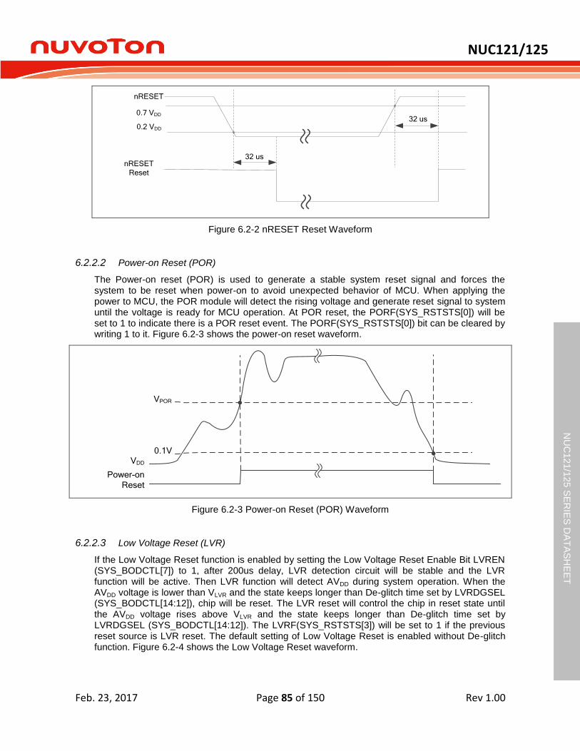
NUC121/125
Feb. 23, 2017 Page 85 of 150 Rev 1.00
NU
C12
1/1
25 S
ER
IES
DA
TA
SH
EE
T
nRESET
0.2 VDD
0.7 VDD
nRESET
Reset
32 us
32 us
Figure 6.2-2 nRESET Reset Waveform
Power-on Reset (POR) 6.2.2.2
The Power-on reset (POR) is used to generate a stable system reset signal and forces the system to be reset when power-on to avoid unexpected behavior of MCU. When applying the power to MCU, the POR module will detect the rising voltage and generate reset signal to system until the voltage is ready for MCU operation. At POR reset, the PORF(SYS_RSTSTS[0]) will be set to 1 to indicate there is a POR reset event. The PORF(SYS_RSTSTS[0]) bit can be cleared by writing 1 to it. Figure 6.2-3 shows the power-on reset waveform.
VDD
VPOR
Power-on
Reset
0.1V
Figure 6.2-3 Power-on Reset (POR) Waveform
Low Voltage Reset (LVR) 6.2.2.3
If the Low Voltage Reset function is enabled by setting the Low Voltage Reset Enable Bit LVREN (SYS_BODCTL[7]) to 1, after 200us delay, LVR detection circuit will be stable and the LVR function will be active. Then LVR function will detect AVDD during system operation. When the AVDD voltage is lower than VLVR and the state keeps longer than De-glitch time set by LVRDGSEL (SYS_BODCTL[14:12]), chip will be reset. The LVR reset will control the chip in reset state until the AVDD voltage rises above VLVR and the state keeps longer than De-glitch time set by LVRDGSEL (SYS_BODCTL[14:12]). The LVRF(SYS_RSTSTS[3]) will be set to 1 if the previous reset source is LVR reset. The default setting of Low Voltage Reset is enabled without De-glitch function. Figure 6.2-4 shows the Low Voltage Reset waveform.
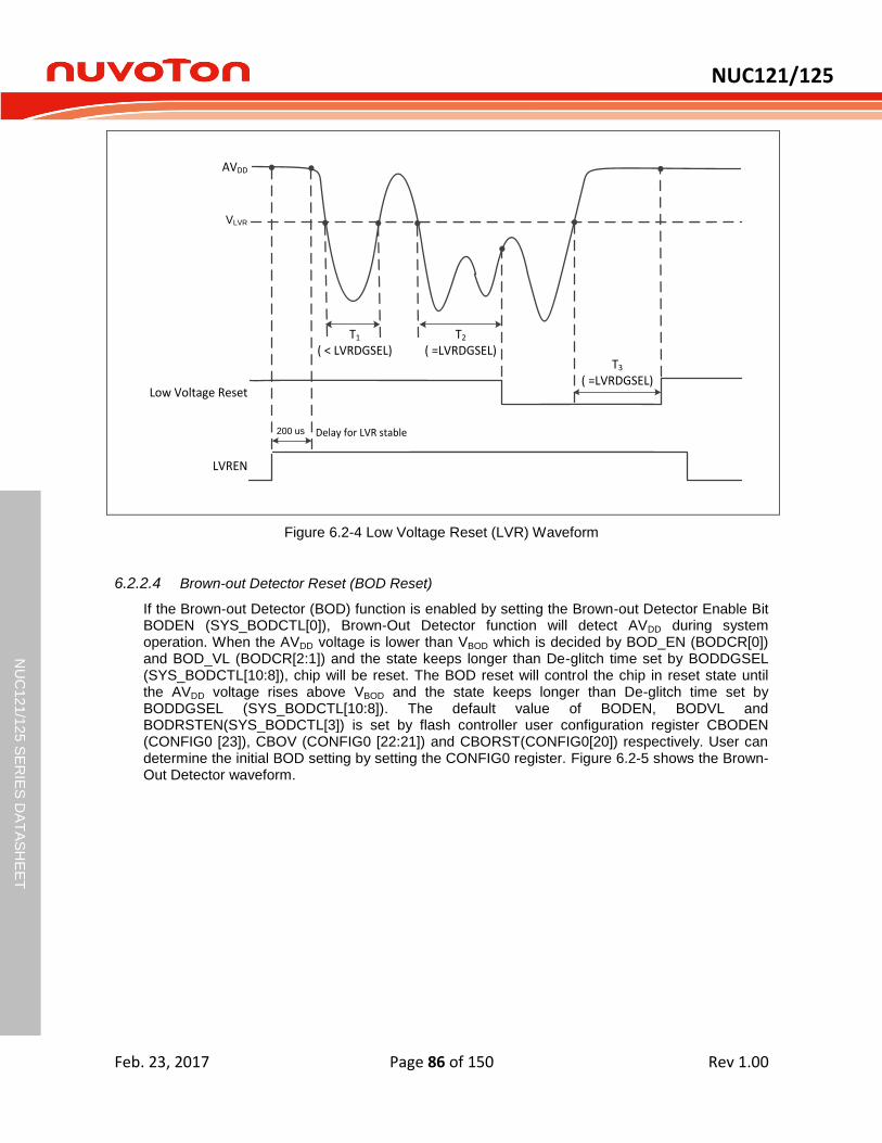
NUC121/125
Feb. 23, 2017 Page 86 of 150 Rev 1.00
NU
C12
1/1
25 S
ER
IES
DA
TA
SH
EE
T
AVDD
VLVR
Low Voltage Reset
T1
( < LVRDGSEL)T2
( =LVRDGSEL)T3
( =LVRDGSEL)
LVREN
200 us Delay for LVR stable
Figure 6.2-4 Low Voltage Reset (LVR) Waveform
Brown-out Detector Reset (BOD Reset) 6.2.2.4
If the Brown-out Detector (BOD) function is enabled by setting the Brown-out Detector Enable Bit BODEN (SYS_BODCTL[0]), Brown-Out Detector function will detect AVDD during system operation. When the AVDD voltage is lower than VBOD which is decided by BOD_EN (BODCR[0]) and BOD_VL (BODCR[2:1]) and the state keeps longer than De-glitch time set by BODDGSEL (SYS_BODCTL[10:8]), chip will be reset. The BOD reset will control the chip in reset state until the AVDD voltage rises above VBOD and the state keeps longer than De-glitch time set by BODDGSEL (SYS_BODCTL[10:8]). The default value of BODEN, BODVL and BODRSTEN(SYS_BODCTL[3]) is set by flash controller user configuration register CBODEN (CONFIG0 [23]), CBOV (CONFIG0 [22:21]) and CBORST(CONFIG0[20]) respectively. User can determine the initial BOD setting by setting the CONFIG0 register. Figure 6.2-5 shows the Brown-Out Detector waveform.
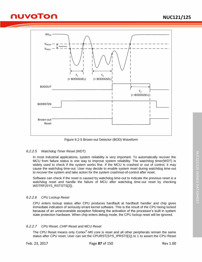
NUC121/125
Feb. 23, 2017 Page 87 of 150 Rev 1.00
NU
C12
1/1
25 S
ER
IES
DA
TA
SH
EE
T
AVDD
VBODL
BODOUT
BODRSTEN
Brown-out Reset
T1
(< BODDGSEL)T2
(= BODDGSEL)
T3
(= BODDGSEL)
HysteresisVBODH
Figure 6.2-5 Brown-out Detector (BOD) Waveform
Watchdog Timer Reset (WDT) 6.2.2.5
In most industrial applications, system reliability is very important. To automatically recover the MCU from failure status is one way to improve system reliability. The watchdog timer(WDT) is widely used to check if the system works fine. If the MCU is crashed or out of control, it may cause the watchdog time-out. User may decide to enable system reset during watchdog time-out to recover the system and take action for the system crash/out-of-control after reset.
Software can check if the reset is caused by watchdog time-out to indicate the previous reset is a watchdog reset and handle the failure of MCU after watchdog time-out reset by checking WDTRF(SYS_RSTSTS[2]).
CPU Lockup Reset 6.2.2.6
CPU enters lockup status after CPU produces hardfault at hardfault handler and chip gives immediate indication of seriously errant kernel software. This is the result of the CPU being locked because of an unrecoverable exception following the activation of the processor’s built in system state protection hardware. When chip enters debug mode, the CPU lockup reset will be ignored.
CPU Reset, CHIP Reset and MCU Reset 6.2.2.7
The CPU Reset means only Cortex®-M0 core is reset and all other peripherals remain the same
status after CPU reset. User can set the CPURST(SYS_IPRST0[1]) to 1 to assert the CPU Reset
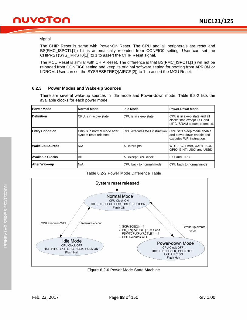
NUC121/125
Feb. 23, 2017 Page 88 of 150 Rev 1.00
NU
C12
1/1
25 S
ER
IES
DA
TA
SH
EE
T
signal.
The CHIP Reset is same with Power-On Reset. The CPU and all peripherals are reset and BS(FMC_ISPCTL[1]) bit is automatically reloaded from CONFIG0 setting. User can set the CHIPRST(SYS_IPRST0[1]) to 1 to assert the CHIP Reset signal.
The MCU Reset is similar with CHIP Reset. The difference is that BS(FMC_ISPCTL[1]) will not be reloaded from CONFIG0 setting and keep its original software setting for booting from APROM or LDROM. User can set the SYSRESETREQ(AIRCR[2]) to 1 to assert the MCU Reset.
6.2.3 Power Modes and Wake-up Sources
There are several wake-up sources in Idle mode and Power-down mode. Table 6.2-2 lists the available clocks for each power mode.
Power Mode Normal Mode Idle Mode Power-Down Mode
Definition CPU is in active state CPU is in sleep state CPU is in sleep state and all clocks stop except LXT and LIRC. SRAM content retended.
Entry Condition Chip is in normal mode after system reset released
CPU executes WFI instruction. CPU sets sleep mode enable and power down enable and executes WFI instruction.
Wake-up Sources N/A All interrupts WDT, I²C, Timer, UART, BOD, GPIO, EINT, USCI and USBD.
Available Clocks All All except CPU clock LXT and LIRC
After Wake-up N/A CPU back to normal mode CPU back to normal mode
Table 6.2-2 Power Mode Difference Table
Normal ModeCPU Clock ON
HXT, HIRC, LXT, LIRC, HCLK, PCLK ON
Flash ON
Power-down ModeCPU Clock OFF
HXT, HIRC, HCLK, PCLK OFF
Flash Halt
System reset released
CPU executes WFI Interrupts occur
Idle ModeCPU Clock OFF
HXT, HIRC, LXT, LIRC, HCLK, PCLK ON
Flash Halt
1. SCR(SCB[2]) = 1
2. PD_EN(PWRCTL[7]) = 1 and
PDWTCPU(PWRCTL[8]) = 1
3. CPU executes WFI
Wake-up events
occur
LXT, LIRC ON
Figure 6.2-6 Power Mode State Machine
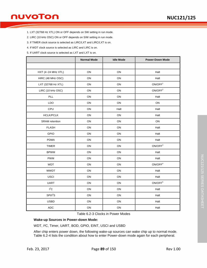
NUC121/125
Feb. 23, 2017 Page 89 of 150 Rev 1.00
NU
C12
1/1
25 S
ER
IES
DA
TA
SH
EE
T
1. LXT (32768 Hz XTL) ON or OFF depends on SW setting in run mode.
2. LIRC (10 kHz OSC) ON or OFF depends on S/W setting in run mode.
3. If TIMER clock source is selected as LIRC/LXT and LIRC/LXT is on.
4. If WDT clock source is selected as LIRC and LIRC is on.
5. If UART clock source is selected as LXT and LXT is on.
Normal Mode Idle Mode Power-Down Mode
HXT (4~24 MHz XTL) ON ON Halt
HIRC (48 MHz OSC) ON ON Halt
LXT (32768 Hz XTL) ON ON ON/OFF1
LIRC (10 kHz OSC) ON ON ON/OFF2
PLL ON ON Halt
LDO ON ON ON
CPU ON Halt Halt
HCLK/PCLK ON ON Halt
SRAM retention ON ON ON
FLASH ON ON Halt
GPIO ON ON Halt
PDMA ON ON Halt
TIMER ON ON ON/OFF3
BPWM ON ON Halt
PWM ON ON Halt
WDT ON ON ON/OFF4
WWDT ON ON Halt
USCI ON ON Halt
UART ON ON ON/OFF5
I2C ON ON Halt
SPI/I2S ON ON Halt
USBD ON ON Halt
ADC ON ON Halt
Table 6.2-3 Clocks in Power Modes
Wake-up Sources in Power-down Mode:
WDT, I²C, Timer, UART, BOD, GPIO, EINT, USCI and USBD
After chip enters power down, the following wake-up sources can wake chip up to normal mode. Table 6.2-4 lists the condition about how to enter Power-down mode again for each peripheral.
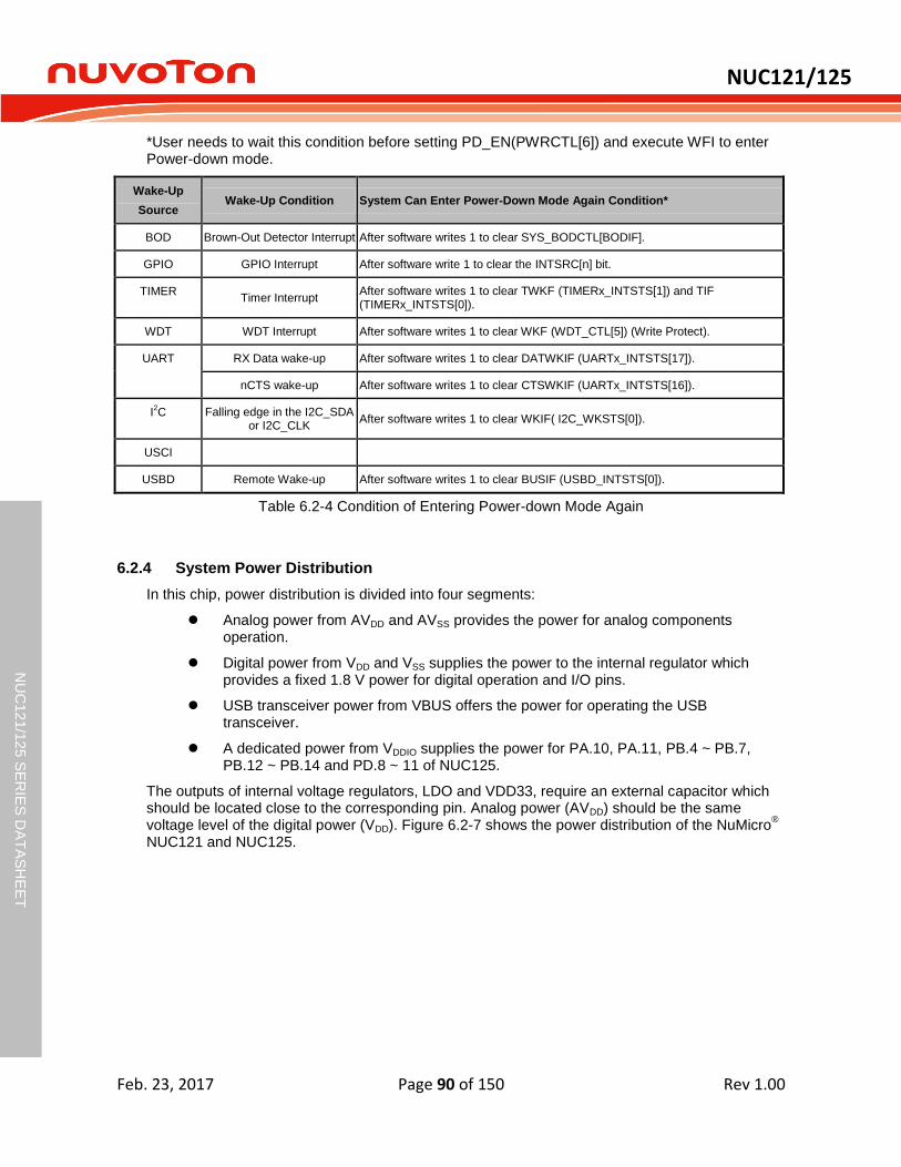
NUC121/125
Feb. 23, 2017 Page 90 of 150 Rev 1.00
NU
C12
1/1
25 S
ER
IES
DA
TA
SH
EE
T
*User needs to wait this condition before setting PD_EN(PWRCTL[6]) and execute WFI to enter Power-down mode.
Wake-Up
Source Wake-Up Condition System Can Enter Power-Down Mode Again Condition*
BOD Brown-Out Detector Interrupt After software writes 1 to clear SYS_BODCTL[BODIF].
GPIO GPIO Interrupt After software write 1 to clear the INTSRC[n] bit.
TIMER Timer Interrupt
After software writes 1 to clear TWKF (TIMERx_INTSTS[1]) and TIF (TIMERx_INTSTS[0]).
WDT WDT Interrupt After software writes 1 to clear WKF (WDT_CTL[5]) (Write Protect).
UART RX Data wake-up After software writes 1 to clear DATWKIF (UARTx_INTSTS[17]).
nCTS wake-up After software writes 1 to clear CTSWKIF (UARTx_INTSTS[16]).
I2C Falling edge in the I2C_SDA
or I2C_CLK After software writes 1 to clear WKIF( I2C_WKSTS[0]).
USCI
USBD Remote Wake-up After software writes 1 to clear BUSIF (USBD_INTSTS[0]).
Table 6.2-4 Condition of Entering Power-down Mode Again
6.2.4 System Power Distribution
In this chip, power distribution is divided into four segments:
Analog power from AVDD and AVSS provides the power for analog components operation.
Digital power from VDD and VSS supplies the power to the internal regulator which provides a fixed 1.8 V power for digital operation and I/O pins.
USB transceiver power from VBUS offers the power for operating the USB transceiver.
A dedicated power from VDDIO supplies the power for PA.10, PA.11, PB.4 ~ PB.7, PB.12 ~ PB.14 and PD.8 ~ 11 of NUC125.
The outputs of internal voltage regulators, LDO and VDD33, require an external capacitor which should be located close to the corresponding pin. Analog power (AVDD) should be the same voltage level of the digital power (VDD). Figure 6.2-7 shows the power distribution of the NuMicro
®
NUC121 and NUC125.
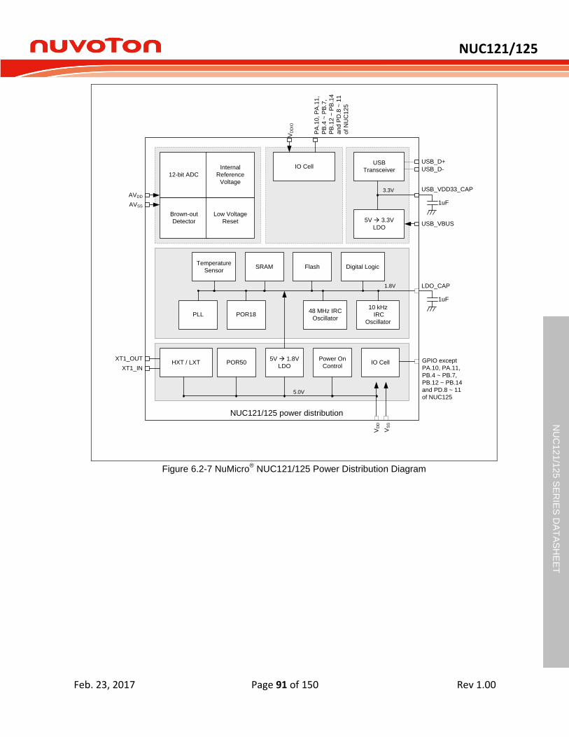
NUC121/125
Feb. 23, 2017 Page 91 of 150 Rev 1.00
NU
C12
1/1
25 S
ER
IES
DA
TA
SH
EE
T
USB
Transceiver
AVDD
AVSS
VD
D
VS
S
USB_VBUS
USB_D+
USB_D-
48 MHz IRC
Oscillator
10 kHz
IRC
Oscillator
SRAM
PLL
5V à 3.3V
LDO
IO Cell5V à 1.8V
LDOPOR50
POR18
Brown-out
Detector
Low Voltage
Reset
Temperature
Sensor
HXT / LXT
Digital LogicFlash
12-bit ADC
Internal
Reference
Voltage
Power On
Control
XT1_OUT
XT1_IN
GPIO except
PA.10, PA.11,
PB.4 ~ PB.7,
PB.12 ~ PB.14
and PD.8 ~ 11
of NUC125
1.8V
3.3V
5.0V
USB_VDD33_CAP
LDO_CAP
1uF
1uF
NUC121/125 power distribution
IO Cell
PA
.10, P
A.1
1,
PB
.4 ~
PB
.7,
PB
.12
~ P
B.1
4
an
d P
D.8
~ 1
1
of N
UC
12
5
VD
DIO
Figure 6.2-7 NuMicro® NUC121/125 Power Distribution Diagram

NUC121/125
Feb. 23, 2017 Page 92 of 150 Rev 1.00
NU
C12
1/1
25 S
ER
IES
DA
TA
SH
EE
T
Clock Controller 6.3
6.3.1 Overview
The clock controller generates clocks for the whole chip, including system clocks and all peripheral clocks. The clock controller also implements the power control function with the individually clock ON/OFF control, clock source selection and a clock divider. The chip will not enter Power-down mode until CPU sets the Power-down enable bit PDEN(CLK_PWRCTL[7]) and Cortex
®-M0 core executes the WFI instruction. After that, chip enters Power-down mode and wait
for wake-up interrupt source triggered to leave Power-down mode. In Power-down mode, the clock controller turns off the 4~24 MHz external high speed crystal (HXT) and 48 MHz internal high speed RC oscillator (HIRC) to reduce the overall system power consumption. Figure 6.3-1 shows the clock generator and the overview of the clock source control.
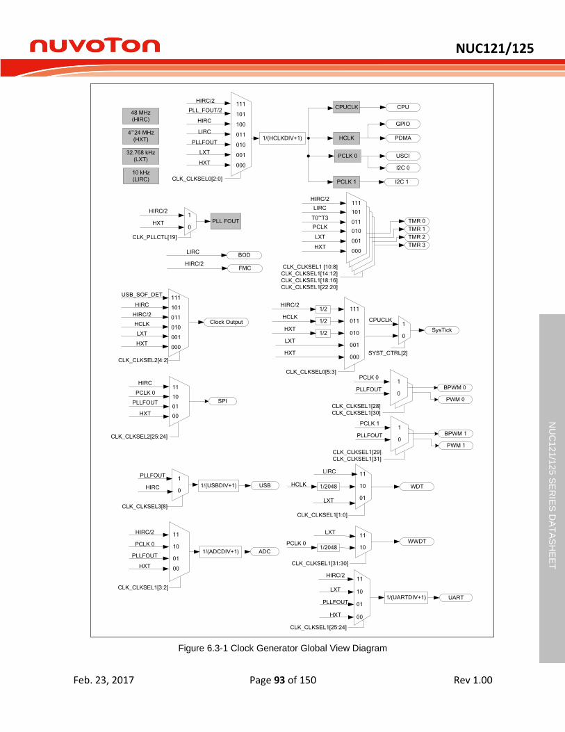
NUC121/125
Feb. 23, 2017 Page 93 of 150 Rev 1.00
NU
C12
1/1
25 S
ER
IES
DA
TA
SH
EE
T
1
0
CLK_PLLCTL[19]
48 MHz
(HIRC)
4~24 MHz
(HXT)
PLL FOUT
111
011
010
001
HXT
LXT
HXT
HCLK
HIRC/2
000
1/2
1/2
1/2
CLK_CLKSEL0[5:3]
1
0SysTick
TMR 3
UART
PDMA
I2C 1
FMC
WDT
PWM 0
BPWM 0
TMR 0
TMR 1
TMR 2
CPU
32.768 kHz
(LXT)
10 kHz
(LIRC)
111
010
001
000
PCLK
LXT
HXT
011
010
001
PLLFOUT
LXT
HXT
LIRC
000
CLK_CLKSEL0[2:0]
SYST_CTRL[2]
CPUCLK
1/(HCLKDIV+1)
PCLK 1
CPUCLK
HCLK
HIRC/2
CLK_CLKSEL1 [10:8]
CLK_CLKSEL1[14:12]
CLK_CLKSEL1[18:16]
CLK_CLKSEL1[22:20]
1
0PLLFOUT
PCLK 0
CLK_CLKSEL1[28]
CLK_CLKSEL1[30]
HIRC/2
LIRC 11
10
CLK_CLKSEL1[1:0]
HCLK 1/2048
1/(UARTDIV+1)
HIRC/2
HXT
01LXT
11
01
00
PLLFOUT
HXT
LXT
CLK_CLKSEL1[25:24]
111HIRC/2
101LIRC
011T0~T3
1/(USBDIV+1)
PLLFOUT
PCLK 0
HXT
HIRC
PLLFOUT
CLK_CLKSEL2[25:24]
11
10
01
00
ADC
PCLK 0
HXT
HIRC/2
PLLFOUT
CLK_CLKSEL1[3:2]
11
10
01
00
BODLIRC
1/(ADCDIV+1)
WWDT
LXT11
10
CLK_CLKSEL1[31:30]
PCLK 01/2048
SPI
100HIRC
101PLL_FOUT/2
USCIPCLK 0
USB
1
0HIRC
CLK_CLKSEL3[8]
I2C 0
GPIO
PWM 1
BPWM 11
0PLLFOUT
PCLK 1
CLK_CLKSEL1[29]
CLK_CLKSEL1[31]
HIRC/2
10
HCLK
HXT
HIRC/2
LXT
CLK_CLKSEL2[4:2]
011
010
001
000
Clock Output
HIRC
USB_SOF_DET111
101
Figure 6.3-1 Clock Generator Global View Diagram
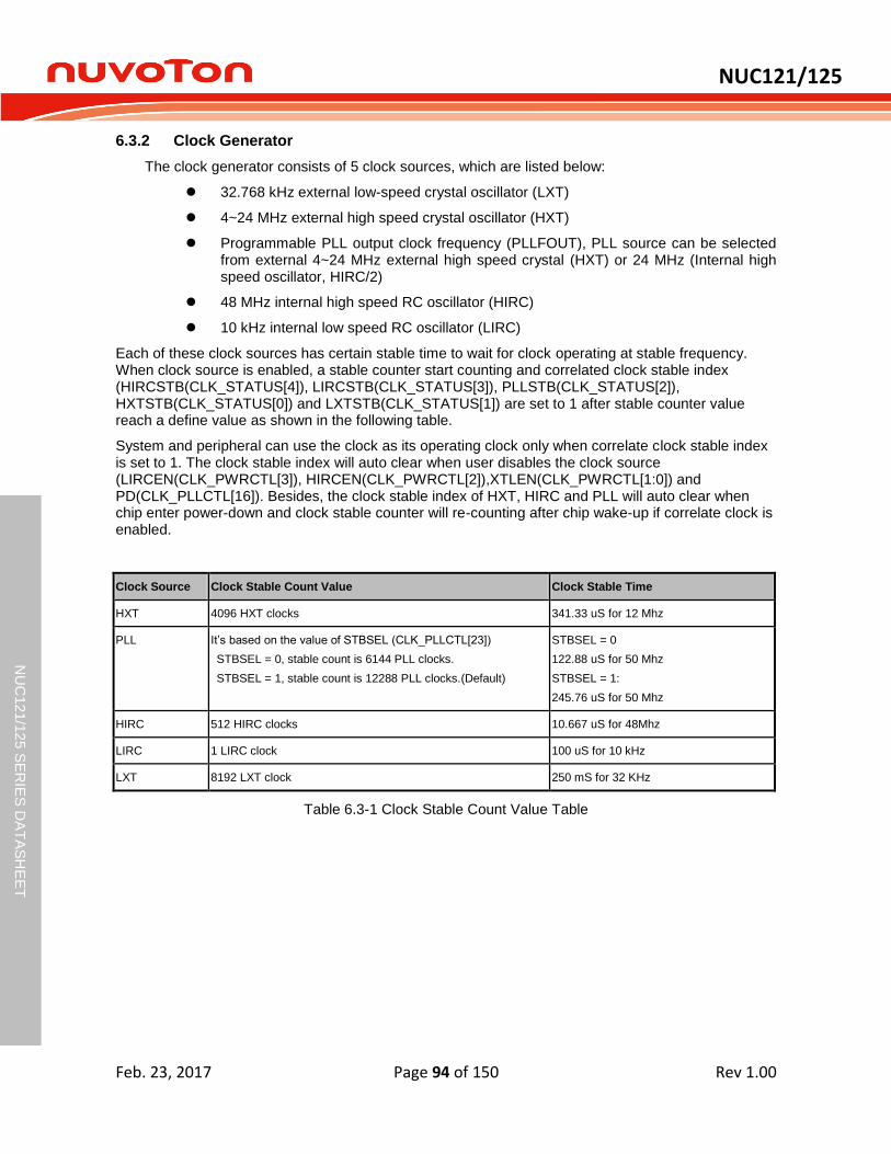
NUC121/125
Feb. 23, 2017 Page 94 of 150 Rev 1.00
NU
C12
1/1
25 S
ER
IES
DA
TA
SH
EE
T
6.3.2 Clock Generator
The clock generator consists of 5 clock sources, which are listed below:
32.768 kHz external low-speed crystal oscillator (LXT)
4~24 MHz external high speed crystal oscillator (HXT)
Programmable PLL output clock frequency (PLLFOUT), PLL source can be selected from external 4~24 MHz external high speed crystal (HXT) or 24 MHz (Internal high speed oscillator, HIRC/2)
48 MHz internal high speed RC oscillator (HIRC)
10 kHz internal low speed RC oscillator (LIRC)
Each of these clock sources has certain stable time to wait for clock operating at stable frequency. When clock source is enabled, a stable counter start counting and correlated clock stable index (HIRCSTB(CLK_STATUS[4]), LIRCSTB(CLK_STATUS[3]), PLLSTB(CLK_STATUS[2]), HXTSTB(CLK_STATUS[0]) and LXTSTB(CLK_STATUS[1]) are set to 1 after stable counter value reach a define value as shown in the following table.
System and peripheral can use the clock as its operating clock only when correlate clock stable index is set to 1. The clock stable index will auto clear when user disables the clock source (LIRCEN(CLK_PWRCTL[3]), HIRCEN(CLK_PWRCTL[2]),XTLEN(CLK_PWRCTL[1:0]) and PD(CLK_PLLCTL[16]). Besides, the clock stable index of HXT, HIRC and PLL will auto clear when chip enter power-down and clock stable counter will re-counting after chip wake-up if correlate clock is enabled.
Clock Source Clock Stable Count Value Clock Stable Time
HXT 4096 HXT clocks 341.33 uS for 12 Mhz
PLL It’s based on the value of STBSEL (CLK_PLLCTL[23])
STBSEL = 0, stable count is 6144 PLL clocks.
STBSEL = 1, stable count is 12288 PLL clocks.(Default)
STBSEL = 0
122.88 uS for 50 Mhz
STBSEL = 1:
245.76 uS for 50 Mhz
HIRC 512 HIRC clocks 10.667 uS for 48Mhz
LIRC 1 LIRC clock 100 uS for 10 kHz
LXT 8192 LXT clock 250 mS for 32 KHz
Table 6.3-1 Clock Stable Count Value Table
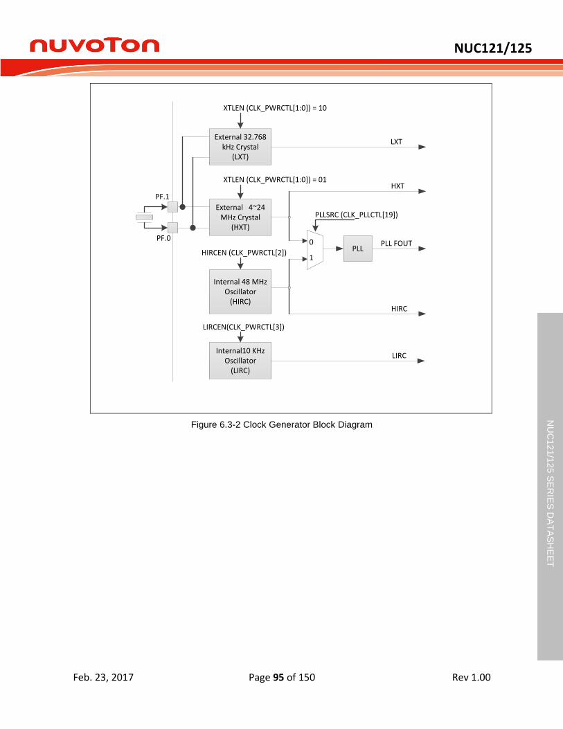
NUC121/125
Feb. 23, 2017 Page 95 of 150 Rev 1.00
NU
C12
1/1
25 S
ER
IES
DA
TA
SH
EE
T
PF.0
External 4~24 MHz Crystal
(HXT)
XTLEN (CLK_PWRCTL[1:0]) = 01
PF.1
Internal 48 MHzOscillator
(HIRC)
HIRCEN (CLK_PWRCTL[2])
0
1PLL
PLLSRC (CLK_PLLCTL[19])
PLL FOUT
External 32.768 kHz Crystal
(LXT)
LXT
XTLEN (CLK_PWRCTL[1:0]) = 10
Internal10 KHz Oscillator
(LIRC)
LIRCEN(CLK_PWRCTL[3])
HXT
HIRC
LIRC
Figure 6.3-2 Clock Generator Block Diagram
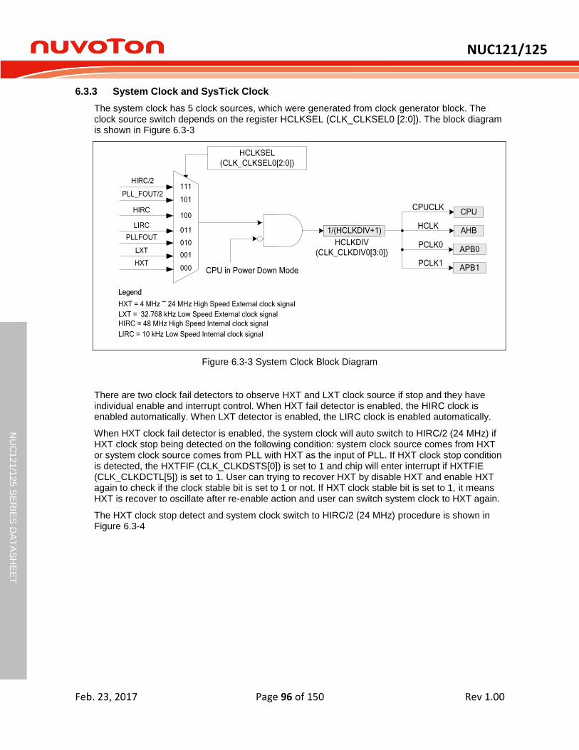
NUC121/125
Feb. 23, 2017 Page 96 of 150 Rev 1.00
NU
C12
1/1
25 S
ER
IES
DA
TA
SH
EE
T
6.3.3 System Clock and SysTick Clock
The system clock has 5 clock sources, which were generated from clock generator block. The clock source switch depends on the register HCLKSEL (CLK_CLKSEL0 [2:0]). The block diagram is shown in Figure 6.3-3
HCLKSEL
(CLK_CLKSEL0[2:0])
1/(HCLK_N+1)
HCLKDIV
(CLK_CLKDIV0[3:0])
CPU in Power Down Mode
CPU
AHB
APB1
CPUCLK
HCLK
PCLK1
1/(HCLK_N+1)1/(HCLKDIV+1)011
010
001
PLLFOUT
LXT
HXT
LIRC
000
111HIRC/2
100HIRC
101PLL_FOUT/2
APB0PCLK0
Legend:
HIRC = 48 MHz High Speed Internal clock signal
HXT = 4 MHz ~ 24 MHz High Speed External clock signal
LIRC = 10 kHz Low Speed Internal clock signal
LXT = 32.768 kHz Low Speed External clock signal
Figure 6.3-3 System Clock Block Diagram
There are two clock fail detectors to observe HXT and LXT clock source if stop and they have individual enable and interrupt control. When HXT fail detector is enabled, the HIRC clock is enabled automatically. When LXT detector is enabled, the LIRC clock is enabled automatically.
When HXT clock fail detector is enabled, the system clock will auto switch to HIRC/2 (24 MHz) if HXT clock stop being detected on the following condition: system clock source comes from HXT or system clock source comes from PLL with HXT as the input of PLL. If HXT clock stop condition is detected, the HXTFIF (CLK_CLKDSTS[0]) is set to 1 and chip will enter interrupt if HXTFIE (CLK_CLKDCTL[5]) is set to 1. User can trying to recover HXT by disable HXT and enable HXT again to check if the clock stable bit is set to 1 or not. If HXT clock stable bit is set to 1, it means HXT is recover to oscillate after re-enable action and user can switch system clock to HXT again.
The HXT clock stop detect and system clock switch to HIRC/2 (24 MHz) procedure is shown in Figure 6.3-4
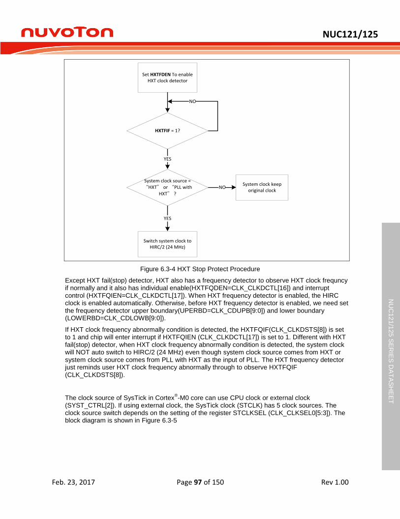
NUC121/125
Feb. 23, 2017 Page 97 of 150 Rev 1.00
NU
C12
1/1
25 S
ER
IES
DA
TA
SH
EE
T
Set HXTFDEN To enable HXT clock detector
HXTFIF = 1?
System clock source =“HXT” or “PLL with
HXT” ?
YES
System clock keep original clock
NO
YES
Switch system clock to HIRC/2 (24 MHz)
NO
Figure 6.3-4 HXT Stop Protect Procedure
Except HXT fail(stop) detector, HXT also has a frequency detector to observe HXT clock frequncy if normally and it also has individual enable(HXTFQDEN=CLK_CLKDCTL[16]) and interrupt control (HXTFQIEN=CLK_CLKDCTL[17]). When HXT frequency detector is enabled, the HIRC clock is enabled automatically. Otherwise, before HXT frequency detector is enabled, we need set the frequency detector upper boundary(UPERBD=CLK_CDUPB[9:0]) and lower boundary (LOWERBD=CLK_CDLOWB[9:0]).
If HXT clock frequency abnormally condition is detected, the HXTFQIF(CLK_CLKDSTS[8]) is set to 1 and chip will enter interrupt if HXTFQIEN (CLK_CLKDCTL[17]) is set to 1. Different with HXT fail(stop) detector, when HXT clock frequency abnormally condition is detected, the system clock will NOT auto switch to HIRC/2 (24 MHz) even though system clock source comes from HXT or system clock source comes from PLL with HXT as the input of PLL. The HXT frequency detector just reminds user HXT clock frequency abnormally through to observe HXTFQIF (CLK_CLKDSTS[8]).
The clock source of SysTick in Cortex®-M0 core can use CPU clock or external clock
(SYST_CTRL[2]). If using external clock, the SysTick clock (STCLK) has 5 clock sources. The clock source switch depends on the setting of the register STCLKSEL (CLK_CLKSEL0[5:3]). The block diagram is shown in Figure 6.3-5
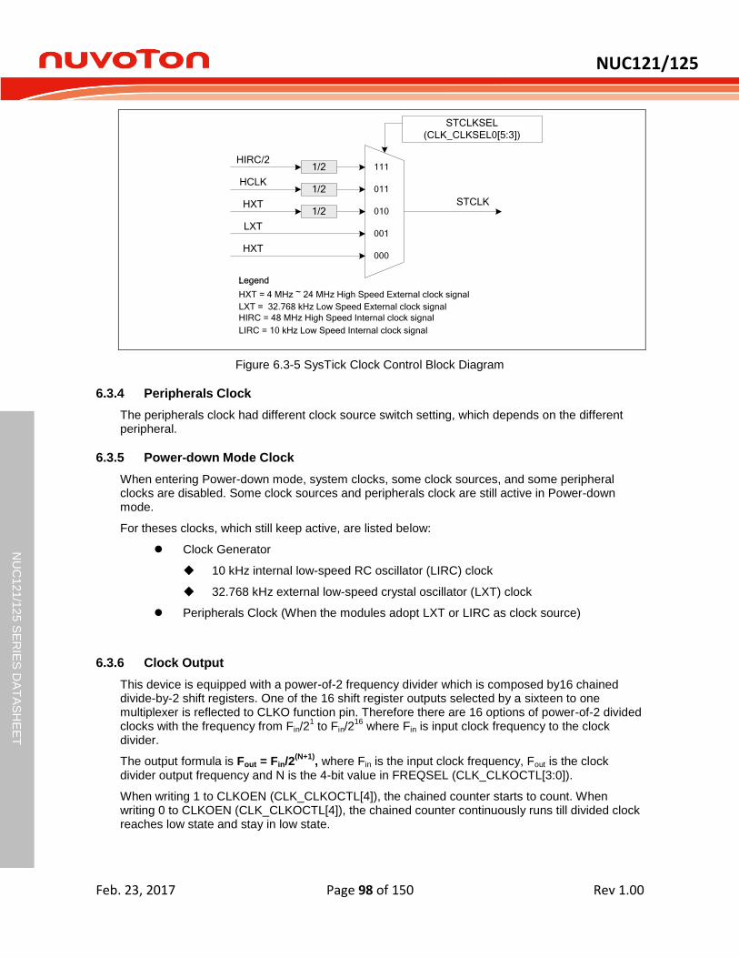
NUC121/125
Feb. 23, 2017 Page 98 of 150 Rev 1.00
NU
C12
1/1
25 S
ER
IES
DA
TA
SH
EE
T
111
011
010
001
HXT
LXT
HXT
HCLK
STCLKSEL
(CLK_CLKSEL0[5:3])
STCLK
HIRC/2
000
1/2
1/2
1/2
Legend:
HIRC = 48 MHz High Speed Internal clock signal
HXT = 4 MHz ~ 24 MHz High Speed External clock signal
LIRC = 10 kHz Low Speed Internal clock signal
LXT = 32.768 kHz Low Speed External clock signal
Figure 6.3-5 SysTick Clock Control Block Diagram
6.3.4 Peripherals Clock
The peripherals clock had different clock source switch setting, which depends on the different peripheral.
6.3.5 Power-down Mode Clock
When entering Power-down mode, system clocks, some clock sources, and some peripheral clocks are disabled. Some clock sources and peripherals clock are still active in Power-down mode.
For theses clocks, which still keep active, are listed below:
Clock Generator
10 kHz internal low-speed RC oscillator (LIRC) clock
32.768 kHz external low-speed crystal oscillator (LXT) clock
Peripherals Clock (When the modules adopt LXT or LIRC as clock source)
6.3.6 Clock Output
This device is equipped with a power-of-2 frequency divider which is composed by16 chained divide-by-2 shift registers. One of the 16 shift register outputs selected by a sixteen to one multiplexer is reflected to CLKO function pin. Therefore there are 16 options of power-of-2 divided clocks with the frequency from Fin/2
1 to Fin/2
16 where Fin is input clock frequency to the clock
divider.
The output formula is Fout = Fin/2(N+1)
, where Fin is the input clock frequency, Fout is the clock divider output frequency and N is the 4-bit value in FREQSEL (CLK_CLKOCTL[3:0]).
When writing 1 to CLKOEN (CLK_CLKOCTL[4]), the chained counter starts to count. When writing 0 to CLKOEN (CLK_CLKOCTL[4]), the chained counter continuously runs till divided clock reaches low state and stay in low state.
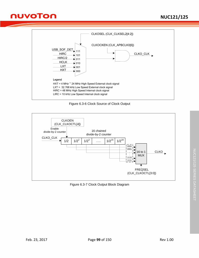
NUC121/125
Feb. 23, 2017 Page 99 of 150 Rev 1.00
NU
C12
1/1
25 S
ER
IES
DA
TA
SH
EE
T
011
010
001
000
HCLK
LXT
HXT
HIRC/2
CLKOSEL (CLK_CLKSEL2[4:2])
CLKOCKEN (CLK_APBCLK0[6])
CLKO_CLK111
101HIRC
USB_SOF_DET
Legend:
HIRC = 48 MHz High Speed Internal clock signal
HXT = 4 MHz ~ 24 MHz High Speed External clock signal
LIRC = 10 kHz Low Speed Internal clock signal
LXT = 32.768 kHz Low Speed External clock signal
Figure 6.3-6 Clock Source of Clock Output
0000
0001
1110
1111
:
:
16 to 1
MUX
1/2 1/22
1/23
1/215
1/216
…...
FREQSEL
(CLK_CLKOCTL[3:0])
CLKO
CLKO_CLK
16 chained
divide-by-2 counter
CLKOEN
(CLK_CLKOCTL[4])
Enable
divide-by-2 counter
Figure 6.3-7 Clock Output Block Diagram
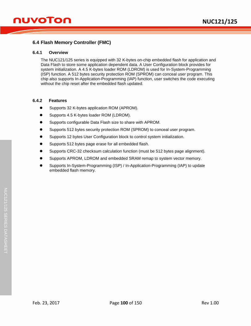
NUC121/125
Feb. 23, 2017 Page 100 of 150 Rev 1.00
NU
C12
1/1
25 S
ER
IES
DA
TA
SH
EE
T
Flash Memory Controller (FMC) 6.4
6.4.1 Overview
The NUC121/125 series is equipped with 32 K-bytes on-chip embedded flash for application and Data Flash to store some application dependent data. A User Configuration block provides for system initialization. A 4.5 K-bytes loader ROM (LDROM) is used for In-System-Programming (ISP) function. A 512 bytes security protection ROM (SPROM) can conceal user program. This chip also supports In-Application-Programming (IAP) function, user switches the code executing without the chip reset after the embedded flash updated.
6.4.2 Features
Supports 32 K-bytes application ROM (APROM).
Supports 4.5 K-bytes loader ROM (LDROM).
Supports configurable Data Flash size to share with APROM.
Supports 512 bytes security protection ROM (SPROM) to conceal user program.
Supports 12 bytes User Configuration block to control system initialization.
Supports 512 bytes page erase for all embedded flash.
Supports CRC-32 checksum calculation function (must be 512 bytes page alignment).
Supports APROM, LDROM and embedded SRAM remap to system vector memory.
Supports In-System-Programming (ISP) / In-Application-Programming (IAP) to update embedded flash memory.
NUC121/125
Feb. 23, 2017 Page 101 of 150 Rev 1.00
NU
C12
1/1
25 S
ER
IES
DA
TA
SH
EE
T
General Purpose I/O (GPIO) 6.5
6.5.1 Overview
The NUC121/125 series has up to 52 General Purpose I/O pins to be shared with other function pins depending on the chip configuration. These 52 pins are arranged in 6 ports named as PA, PB, PC, PD, PE and PF.
PA has 6 pins on port (PA.10 ~ PA.15).
PB has 15 pins on port (PB.0 ~ PB.15, exclude PB.11).
PC has 12 pins on port (PC.0 ~ PC.13, exclude PC.6, PC.7).
PD has 10 pins on port (PD.0 ~ PD.11, exclude PD.6, PD.7).
PE has 3 pins on port (PE.0 ~ PE.2).
PF has 6 pins on port (PF.0 ~ PF.5).
Each of the 52 pins is independent and has the corresponding register bits to control the pin mode function and data
The I/O type of each of I/O pins can be configured by software individually as Input, Push-pull output, Open-drain output or Quasi-bidirectional mode. After the chip is reset, the I/O mode of all pins are depending on CIOIN (CONFIG0[10]). Each I/O pin has a very weakly individual pull-up
resistor which is about 110 k ~ 300 k for VDD is from 5.0 V to 2.5 V.
6.5.2 Features
Four I/O modes:
Quasi-bidirectional mode
Push-Pull Output mode
Open-Drain Output mode
Input mode
TTL/Schmitt trigger input selectable
I/O pin can be configured as interrupt source with edge/level setting
Supports High Slew Rate I/O mode
Supports High Drive Strength mode for Port C
Configurable default I/O mode of all pins after reset by CIOINI (CONFIG0[10]) setting
CIOIN = 0, all GPIO pins in input mode after chip reset
CIOIN = 1, all GPIO pins in Quasi-bidirectional mode after chip reset
I/O pin internal pull-up resistor enabled only in Quasi-bidirectional I/O mode
Enabling the pin interrupt function will also enable the wake-up function
NUC121/125
Feb. 23, 2017 Page 102 of 150 Rev 1.00
NU
C12
1/1
25 S
ER
IES
DA
TA
SH
EE
T
PDMA Controller (PDMA) 6.6
6.6.1 Overview
The peripheral direct memory access (PDMA) controller is used to provide high-speed data transfer. The PDMA controller can transfer data from one address to another without CPU intervention. This has the benefit of reducing the workload of CPU and keeps CPU resources free for other applications. The PDMA controller has a total of 5 channels and each channel can perform transfer between memory and peripherals or between memory and memory. The PDMA supports time-out function for channel 0 and channel 1.
6.6.2 Features
Supports 5 independently configurable channels
Supports selectable 2 level of priority (fixed priority or round-robin priority)
Supports transfer data width of 8, 16, and 32 bits
Supports source and destination address increment size can be byte, half-word, word or no increment
Supports software and SPI, UART, I2S, I
2C, USCI, ADC, PWM and TIMER request
Supports Scatter-Gather mode to perform sophisticated transfer through the use of the descriptor link list table
Supports single and burst transfer type
Supports time-out function for channel 0 and channel 1
NUC121/125
Feb. 23, 2017 Page 103 of 150 Rev 1.00
NU
C12
1/1
25 S
ER
IES
DA
TA
SH
EE
T
Timer Controller (TMR) 6.7
6.7.1 Overview
The Timer controller includes four 32-bit timers, Timer0 ~ Timer3, allowing user to easily implement a timer control for applications. The timer can perform functions, such as frequency measurement, delay timing, clock generation, and event counting by external input pins, and interval measurement by external capture pins.
6.7.2 Features
Four sets of 32-bit timers with 24-bit up counter and one 8-bit prescale counter
Independent clock source for each timer
Provides one-shot, periodic, toggle-output and continuous counting operation modes
24-bit up counter value is readable through CNT (TIMERx_CNT[23:0])
Supports event counting function
24-bit capture value is readable through CAPDAT (TIMERx_CAP[23:0])
Supports external capture pin event for interval measurement
Supports external capture pin event to reset 24-bit up counter
Supports chip wake-up from Idle/Power-down mode if a timer interrupt signal is generated
Support Timer0 ~ Timer3 time-out interrupt signal or capture interrupt signal to trigger PWM, BPWM, PDMA, ADC and DAC function
NUC121/125
Feb. 23, 2017 Page 104 of 150 Rev 1.00
NU
C12
1/1
25 S
ER
IES
DA
TA
SH
EE
T
Basic PWM Generator and Capture Timer (BPWM) 6.8
6.8.1 Overview
The NUC121/125 series provides two BPWM generators: BPWM0 and BPWM1. Each BPWM supports 6 channels of BPWM output or input capture. There is a 12-bit prescaler to support flexible clock to the 16-bit BPWM counter with 16-bit comparator. The BPWM counter supports up, down and up-down counter types, all 6 channels share one counter. BPWM uses the comparator compared with counter to generate events. These events are used to generate BPWM pulse, interrupt and trigger signal for ADC to start conversion. For BPWM output control unit, it supports polarity output, independent pin mask and tri-state output enable.
The BPWM generator also supports input capture function to latch BPWM counter value to corresponding register when input channel has a rising transition, falling transition or both transition is happened.
6.8.2 Features
BPWM function features 6.8.2.1
Supports maximum clock frequency up to100 MHz
Supports up to two BPWM modules, each module provides 6 output channels
Supports independent mode for BPWM output/Capture input channel
Supports 12-bit pre-scalar from 1 to 4096
Supports 16-bit resolution BPWM counter, each module provides 1 BPWM counter
Up, down and up/down counter operation type
Supports mask function and tri-state enable for each BPWM pin
Supports interrupt on the following events:
BPWM counter match zero, period value or compared value
Supports trigger ADC on the following events:
BPWM counter match zero, period value or compared value
Capture Function Features 6.8.2.2
Supports up to 12 capture input channels with 16-bit resolution
Supports rising edge or falling edge or both edges capture condition
Supports input rising/falling edge or both edges capture interrupt
Supports rising/falling or both edges capture with counter reload option
NUC121/125
Feb. 23, 2017 Page 105 of 150 Rev 1.00
NU
C12
1/1
25 S
ER
IES
DA
TA
SH
EE
T
PWM Generator and Capture Timer (PWM) 6.9
6.9.1 Overview
The NUC121/125 series provides two PWM generators - PWM0 and PWM1. Each PWM
supports 6 channels of PWM output or input capture. There is a 12-bit prescaler to support flexible clock to the 16-bit PWM counter with 16-bit comparator. The PWM counter supports up, down and up-down counter types. PWM uses the comparator compared with counter to generate events. These events are used to generate PWM pulse, interrupt and trigger signal for ADC to start conversion.
The PWM generator supports two standard PWM output modes: Independent mode and Complementary mode, which have difference architecture. In Complementary mode, there are two comparators to generate various PWM pulse with 12-bit dead-time generator. For PWM output control unit, it supports polarity output, independent pin mask, tri-state output enable and brake functions.
The PWM generator also supports input capture function to latch PWM counter value to the corresponding register when input channel has a rising transition, falling transition or both transition is happened.
6.9.2 Features
PWM function features 6.9.2.1
Supports maximum clock frequency up to100 MHz
Supports up to two PWM modules, each module provides 6 output channels
Supports independent mode for PWM output/Capture input channel
Supports complementary mode for 3 complementary paired PWM output channel
Dead-time insertion with 12-bit resolution
Two compared values during one period
Supports 12-bit pre-scalar from 1 to 4096
Supports 16-bit resolution PWM counter, each module provides 3 PWM counters
Up, down and up/down counter operation type
Supports mask function and tri-state enable for each PWM pin
Supports brake function
Brake source from pin and system safety events (clock failed, Brown-out detection and CPU lockup)
Noise filter for brake source from pin
Edge detect brake source to control brake state until brake interrupt cleared
Level detect brake source to auto recover function after brake condition removed
Supports interrupt on the following events:
PWM counter match zero, period value or compared value
Brake condition happened
Supports trigger ADC on the following events:
PWM counter match zero, period value or compared value
NUC121/125
Feb. 23, 2017 Page 106 of 150 Rev 1.00
NU
C12
1/1
25 S
ER
IES
DA
TA
SH
EE
T
Capture Function Features 6.9.2.2
Supports up to 12 capture input channels with 16-bit resolution
Supports rising or falling capture condition
Supports input rising/falling capture interrupt
Supports rising/falling capture with counter reload option
NUC121/125
Feb. 23, 2017 Page 107 of 150 Rev 1.00
NU
C12
1/1
25 S
ER
IES
DA
TA
SH
EE
T
Watchdog Timer (WDT) 6.10
6.10.1 Overview
The purpose of Watchdog Timer (WDT) is to perform a system reset when system runs into an unknown state. This prevents system from hanging for an infinite period of time. Besides, this Watchdog Timer supports the function to wake-up system from Idle/Power-down mode.
6.10.2 Features
18-bit free running up counter for WDT time-out interval.
Selectable time-out interval (24 ~ 2
18) and the time-out interval is 1.6 ms ~ 26.214 s if
WDT_CLK = 10 kHz.
System kept in reset state for a period of (1 / WDT_CLK) * 63.
Supports selectable WDT reset delay period, including 1026, 130, 18 or 3 WDT_CLK reset delay period.
Supports to force WDT enabled after chip powered on or reset by setting CWDTEN[2:0] in Config0 register.
Supports WDT time-out wake-up function only if WDT clock source is selected as LIRC or LXT.

NUC121/125
Feb. 23, 2017 Page 108 of 150 Rev 1.00
NU
C12
1/1
25 S
ER
IES
DA
TA
SH
EE
T
Window Watchdog Timer (WWDT) 6.11
6.11.1 Overview
The Window Watchdog Timer (WWDT) is used to perform a system reset within a specified window period to prevent software run to uncontrollable status by any unpredictable condition.
6.11.2 Features
6-bit down counter value CNTDAT(WWDT_CNT[5:0]) and maximum 6-bit compare value CMPDAT(WWDT_CTL[21:16]) to make the WWDT time-out window period flexible
Supports 4-bit value PSCSEL(WWDT_CTL[11:8]) to programmable maximum 11-bit prescale counter period of WWDT counter
WWDT counter suspends in Idle/Power-down mode
WWDT counter only can be reloaded within in valid window period to prevent system reset
NUC121/125
Feb. 23, 2017 Page 109 of 150 Rev 1.00
NU
C12
1/1
25 S
ER
IES
DA
TA
SH
EE
T
USCI - Universal Serial Control Interface Controller 6.12
6.12.1 Overview
The Universal Serial Control Interface (USCI) is a flexible interface module covering several serial communication protocols. The user can configure this controller as UART, SPI, or I
2C functional
protocol.
6.12.2 Features
The controller can be individually configured to match the application needs. The following protocols are supported:
UART
SPI
I2C
To increase readability, the registers of USCI have different alias names that depending on the selected protocol. For example, register USCI_CTL has alias name UUART_CTL for protocol UART, has alias name USPI_CTL for protocol SPI, and has alias name UI2C_CTL for protocol I2C.
NUC121/125
Feb. 23, 2017 Page 110 of 150 Rev 1.00
NU
C12
1/1
25 S
ER
IES
DA
TA
SH
EE
T
USCI - UART Mode 6.13
6.13.1 Overview
The asynchronous serial channel UART covers the reception and the transmission of asynchronous data frames. It performs a serial-to-parallel conversion on data received from the peripheral, and a parallel-to-serial conversion on data transmitted from the controller. The receiver and transmitter are independent, frames can start at different points in time for transmission and reception.
The UART controller also provides auto flow control. There are two conditions to wake-up the system by incoming data or nCTS.
6.13.2 Features
Supports one transmit buffer and two receive buffer for data payload
Supports hardware auto flow control function
Supports programmable baud-rate generator
Supports 9-Bit Data Transfer (9-Bit RS-485)
Supports baud rate detection by built-in capture event of baud rate generator
Supports PDMA capability
Supports Wake-up function (Data and nCTS Wakeup Only)
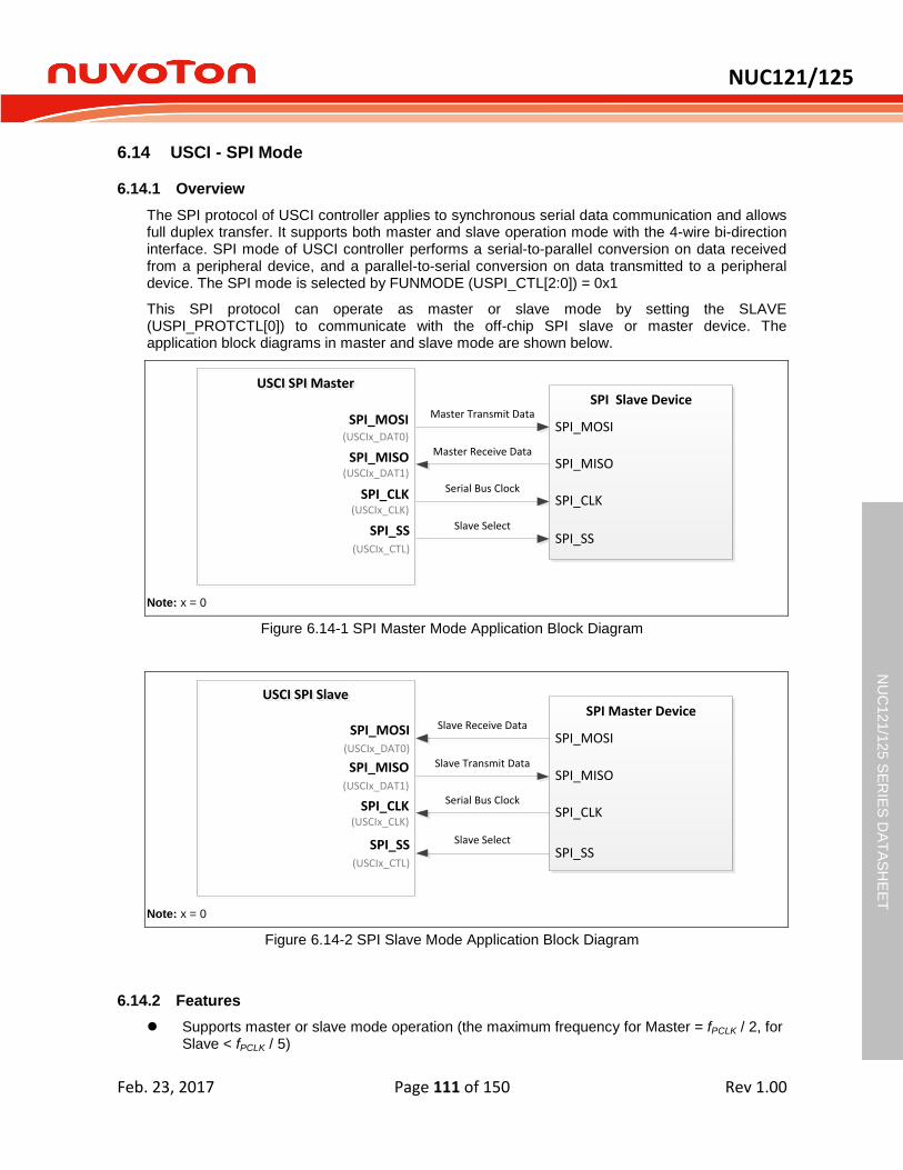
NUC121/125
Feb. 23, 2017 Page 111 of 150 Rev 1.00
NU
C12
1/1
25 S
ER
IES
DA
TA
SH
EE
T
USCI - SPI Mode 6.14
6.14.1 Overview
The SPI protocol of USCI controller applies to synchronous serial data communication and allows full duplex transfer. It supports both master and slave operation mode with the 4-wire bi-direction interface. SPI mode of USCI controller performs a serial-to-parallel conversion on data received from a peripheral device, and a parallel-to-serial conversion on data transmitted to a peripheral device. The SPI mode is selected by FUNMODE (USPI_CTL[2:0]) = 0x1
This SPI protocol can operate as master or slave mode by setting the SLAVE (USPI_PROTCTL[0]) to communicate with the off-chip SPI slave or master device. The application block diagrams in master and slave mode are shown below.
SPI Slave DeviceMaster Transmit Data
Master Receive Data
Serial Bus Clock
Slave Select
SPI_MOSI(USCIx_DAT0)
SPI_MISO(USCIx_DAT1)
SPI_CLK(USCIx_CLK)
SPI_SS(USCIx_CTL)
SPI_MOSI
SPI_MISO
USCI SPI MasterUSCI SPI Master
SPI_CLK
SPI_SS
Note: x = 0
Figure 6.14-1 SPI Master Mode Application Block Diagram
SPI Master DeviceSlave Receive Data
Slave Transmit Data
Serial Bus Clock
Slave Select
SPI_MOSI(USCIx_DAT0)
SPI_MISO(USCIx_DAT1)
SPI_CLK(USCIx_CLK)
SPI_SS(USCIx_CTL)
SPI_MOSI
SPI_MISO
USCI SPI SlaveUSCI SPI Slave
SPI_CLK
SPI_SS
Note: x = 0
Figure 6.14-2 SPI Slave Mode Application Block Diagram
6.14.2 Features
Supports master or slave mode operation (the maximum frequency for Master = fPCLK / 2, for Slave < fPCLK / 5)
NUC121/125
Feb. 23, 2017 Page 112 of 150 Rev 1.00
NU
C12
1/1
25 S
ER
IES
DA
TA
SH
EE
T
Configurable bit length of a transfer word from 4 to 16-bit
Supports one transmit buffer and two receive buffers for data payload
Supports MSB first or LSB first transfer sequence
Supports word suspend function
Supports PDMA transfer
Supports 3-wire, no slave select signal, bi-direction interface
Supports wake-up function by slave select signal in Slave mode
Supports one data channel half-duplex transfer
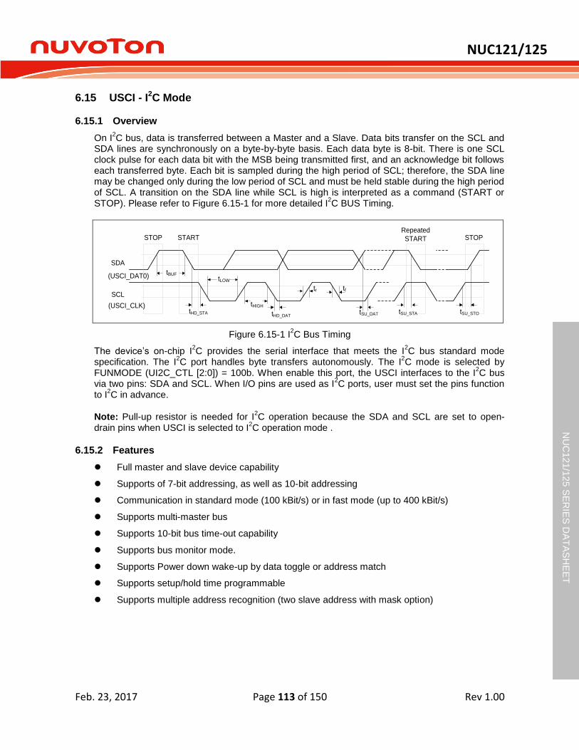
NUC121/125
Feb. 23, 2017 Page 113 of 150 Rev 1.00
NU
C12
1/1
25 S
ER
IES
DA
TA
SH
EE
T
USCI - I2C Mode 6.15
6.15.1 Overview
On I2C bus, data is transferred between a Master and a Slave. Data bits transfer on the SCL and
SDA lines are synchronously on a byte-by-byte basis. Each data byte is 8-bit. There is one SCL clock pulse for each data bit with the MSB being transmitted first, and an acknowledge bit follows each transferred byte. Each bit is sampled during the high period of SCL; therefore, the SDA line may be changed only during the low period of SCL and must be held stable during the high period of SCL. A transition on the SDA line while SCL is high is interpreted as a command (START or STOP). Please refer to Figure 6.15-1 for more detailed I
2C BUS Timing.
tBUF
STOP
SDA
SCL
START
tHD_STA
tLOW
tHD_DAT
tHIGH
tf
tSU_DAT
Repeated
START
tSU_STA tSU_STO
STOP
tr
(USCI_DAT0)
(USCI_CLK)
Figure 6.15-1 I2C Bus Timing
The device’s on-chip I2C provides the serial interface that meets the I
2C bus standard mode
specification. The I2C port handles byte transfers autonomously. The I
2C mode is selected by
FUNMODE (UI2C_CTL [2:0]) = 100b. When enable this port, the USCI interfaces to the I2C bus
via two pins: SDA and SCL. When I/O pins are used as I2C ports, user must set the pins function
to I2C in advance.
Note: Pull-up resistor is needed for I2C operation because the SDA and SCL are set to open-
drain pins when USCI is selected to I2C operation mode .
6.15.2 Features
Full master and slave device capability
Supports of 7-bit addressing, as well as 10-bit addressing
Communication in standard mode (100 kBit/s) or in fast mode (up to 400 kBit/s)
Supports multi-master bus
Supports 10-bit bus time-out capability
Supports bus monitor mode.
Supports Power down wake-up by data toggle or address match
Supports setup/hold time programmable
Supports multiple address recognition (two slave address with mask option)
NUC121/125
Feb. 23, 2017 Page 114 of 150 Rev 1.00
NU
C12
1/1
25 S
ER
IES
DA
TA
SH
EE
T
UART Interface Controller (UART) 6.16
6.16.1 Overview
The NUC121/125 series provides one channel of Universal Asynchronous Receiver/Transmitters (UART). UART controller performs Normal Speed UART and supports flow control function. The UART controller performs a serial-to-parallel conversion on data received from the peripheral and a parallel-to-serial conversion on data transmitted from the CPU. Each UART controller channel supports ten types of interrupts. The UART controller also supports IrDA SIR, LIN and RS-485 function modes and auto-baud rate measuring function.
6.16.2 Features
Full-duplex asynchronous communications
Supports maximum clock frequency up to 10 Mbps
Separates receive and transmit 16/16 bytes entry FIFO for data payloads
Supports hardware auto-flow control
Programmable receiver buffer trigger level
Supports programmable baud rate generator for each channel individually
Supports nCTS, incoming data, Received Data FIFO reached threshold and RS-485 Address Match (AAD mode) wake-up function
Supports 8-bit receiver buffer time-out detection function
Programmable transmitting data delay time between the last stop and the next start bit by setting DLY (UART_TOUT [15:8])
Supports Auto-Baud Rate measurement and baud rate compensation function
Supports break error, frame error, parity error and receive/transmit buffer overflow detection function
Fully programmable serial-interface characteristics
Programmable number of data bit, 5-, 6-, 7-, 8- bit character
Programmable parity bit, even, odd, no parity or stick parity bit generation and detection
Programmable stop bit, 1, 1.5, or 2 stop bit generation
Supports IrDA SIR function mode
Supports for 3/16 bit duration for normal mode
Supports LIN function mode
Supports LIN master/slave mode
Supports programmable break generation function for transmitter
Supports break detection function for receiver
Supports RS-485 function mode
Supports RS-485 9-bit mode
Supports hardware or software enables to program nRTS pin to control RS-485 transmission direction
NUC121/125
Feb. 23, 2017 Page 115 of 150 Rev 1.00
NU
C12
1/1
25 S
ER
IES
DA
TA
SH
EE
T
Supports PDMA transfer function
NUC121/125
Feb. 23, 2017 Page 116 of 150 Rev 1.00
NU
C12
1/1
25 S
ER
IES
DA
TA
SH
EE
T
I2C Serial Interface Controller (I
2C) 6.17
6.17.1 Overview
I2C is a two-wire, bi-directional serial bus that provides a simple and efficient method of data
exchange between devices. The I2C standard is a true multi-master bus including collision
detection and arbitration that prevents data corruption if two or more masters attempt to control the bus simultaneously.
There are two sets of I2C controllers which support Power-down wake-up function.
6.17.2 Features
The I2C bus uses two wires (SDA and SCL) to transfer information between devices connected to
the bus. The main features of the I2C bus include:
Supports up to two I2C ports
Supports speed up to 1Mbps
Master/Slave mode
Bidirectional data transfer between masters and slaves
Multi-master bus (no central master)
Arbitration between simultaneously transmitting masters without corruption of serial data on the bus
Serial clock synchronization allow devices with different bit rates to communicate via one serial bus
Serial clock synchronization used as a handshake mechanism to suspend and resume serial transfer
Built-in 14-bit time-out counter requesting the I2C interrupt if the I
2C bus hangs up and timer-
out counter overflows
Programmable clocks allow for versatile rate control
Supports 7-bit addressing mode
Supports multiple address recognition (four slave address with mask option)
Supports Power-down wake-up function
Supports PDMA with one buffer capability
Supports two-level buffer function
Supports setup/hold time programmable
NUC121/125
Feb. 23, 2017 Page 117 of 150 Rev 1.00
NU
C12
1/1
25 S
ER
IES
DA
TA
SH
EE
T
Serial Peripheral Interface (SPI) 6.18
6.18.1 Overview
The Serial Peripheral Interface (SPI) applies to synchronous serial data communication and allows full duplex transfer. Devices communicate in Master/Slave mode with the 4-wire bi-direction interface. The NUC121/125 series contains one SPI controller performing a serial-to-parallel conversion on data received from a peripheral device, and a parallel-to-serial conversion on data transmitted to a peripheral device. The SPI controller can be configured as a master or a slave device.
This controller also supports the PDMA function to access the data buffer. The SPI controller also supports I
2S mode to connect external audio CODEC.
6.18.2 Features
SPI Mode
One set of SPI controller
Supports Master or Slave mode operation
Configurable bit length of a transaction word from 8 to 32-bit
Provides separate 4-level depth transmit and receive FIFO buffers
Supports MSB first or LSB first transfer sequence
Supports Byte Reorder function
Supports PDMA transfer
Supports one data channel half-duplex transfer
Support receive-only mode
I2S Mode
Supports Master or Slave
Capable of handling 8-, 16-, 24- and 32-bit word sizes
Provides separate 4-level depth transmit and receive FIFO buffers
Supports monaural and stereo audio data
Supports PCM mode A, PCM mode B, I2S and MSB justified data format
Supports PDMA transfer
NUC121/125
Feb. 23, 2017 Page 118 of 150 Rev 1.00
NU
C12
1/1
25 S
ER
IES
DA
TA
SH
EE
T
USB Device Controller (USBD) 6.19
6.19.1 Overview
There is one set of USB 2.0 full-speed device controller and transceiver in this device. It is compliant with USB 2.0 full-speed device specification and supports control/bulk/interrupt/isochronous transfer types. It implements a full-speed (12 Mbit/s) function interface with added support for USB 2.0 Link Power Management.
In this device controller, there are two main interfaces: the APB bus and USB bus which comes from the USB PHY transceiver. For the APB bus, the CPU can program control registers through it. There are 768 bytes internal SRAM as data buffer in this controller. For IN or OUT transfer, it is necessary to write data to SRAM or read data from SRAM through the APB interface or SIE. User needs to set the effective starting address of SRAM for each endpoint buffer through buffer segmentation register (USBD_BUFSEGn, n=0~7).
There are 8 endpoints in this controller. Each of the endpoint can be configured as IN or OUT endpoint. All the operations including Control, Bulk, Interrupt and Isochronous transfer are implemented in this block. The block of “Endpoint Control” is also used to manage the data sequential synchronization, endpoint states, current start address, transaction status, and data buffer status for each endpoint.
There are five different interrupt events in this controller. They are the SOF event, no-event-wake-up, device plug-in or plug-out event, USB events, like IN ACK, OUT ACK etc, and BUS events, like suspend and resume, etc. Any event will cause an interrupt, and users just need to check the related event flags in interrupt event status register (USBD_INTSTS) to acknowledge what kind of interrupt occurring, and then check the related USB Endpoint Status Register (USBD_EPSTS) to acknowledge what kind of event occurring in this endpoint.
A software-disconnect function is also supported for this USB controller. It is used to simulate the disconnection of this device from the host. If user enables SE0 bit (USBD_SE0), the USB controller will force the output of USB_D+ and USB_D- to level low and its function is disabled. After disable the SE0 bit, host will enumerate the USB device again.
For more information on the Universal Serial Bus, please refer to Universal Serial Bus Specification Revision 1.1.
6.19.2 Features
Compliant with USB 2.0 Full-Speed specification
Provides 1 interrupt vector with 5 different interrupt events (NEVWK, VBUSDET, USB, BUS and SOF)
Supports Control/Bulk/Interrupt/Isochronous transfer type
Supports suspend function when no bus activity existing for 3 ms
Supports 8 endpoints for configurable Control/Bulk/Interrupt/Isochronous transfer types and maximum 768 bytes buffer size
Provides remote wake-up capability
Start of Frame (SOF) locked clock pulse generation
Supports USB 2.0 Link Power Management

NUC121/125
Feb. 23, 2017 Page 119 of 150 Rev 1.00
NU
C12
1/1
25 S
ER
IES
DA
TA
SH
EE
T
Analog-to-Digital Converter (ADC) 6.20
6.20.1 Overview
The NUC121/125 series contains one 12-bit successive approximation analog-to-digital converter (SAR A/D converter) with 14 input channels. The A/D converter supports four operation modes: Single, Burst, Single-cycle Scan and Continuous Scan mode. The A/D converter can be started by software, external pin (STADC/PC.8), timer0~3 overflow pulse trigger and PWM trigger.
6.20.2 Features
Analog input voltage range: 0 ~ AVDD.
12-bit resolution and 10-bit accuracy is guaranteed
Up to 12 single-end analog input channels or 6 differential analog input channels
Maximum ADC peripheral clock frequency is 16 MHz
Up to 800k SPS sampling rate
Configurable ADC internal sampling time
Four operation modes:
Single mode: A/D conversion is performed one time on a specified channel.
Burst mode: A/D converter samples and converts the specified single channel and sequentially stores the result in FIFO.
Single-cycle Scan mode: A/D conversion is performed only one cycle on all specified channels with the sequence from the smallest numbered channel to the largest numbered channel.
Continuous Scan mode: A/D converter continuously performs Single-cycle Scan mode until software stops A/D conversion.
An A/D conversion can be started by:
Software Write 1 to ADST bit
External pin (STADC)
Timer 0~3 overflow pulse trigger
PWM trigger with optional start delay period
Each conversion result is held in data register of each channel with valid and overrun indicators.
Conversion result can be compared with specified value and user can select whether to generate an interrupt when conversion result matches the compare register setting.
Two internal channels which are band-gap voltage (VBG) and temperature sensor (VTEMP).
Supports PDMA transfer mode.
Note 1: ADC sampling rate = (ADC peripheral clock frequency) / (total ADC conversion cycle)
Note 2: If the internal channel (VTEMP) is selected to convert, the sampling rate needs to be less than 300k SPS for accurate result.
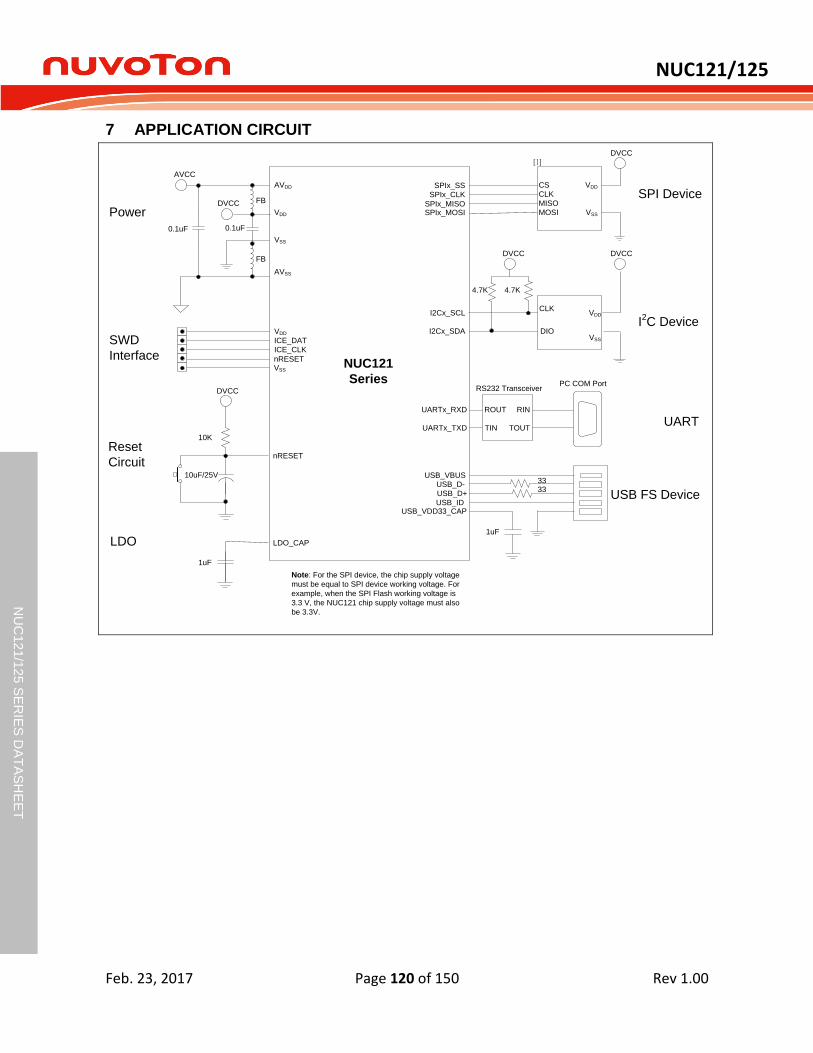
NUC121/125
Feb. 23, 2017 Page 120 of 150 Rev 1.00
NU
C12
1/1
25 S
ER
IES
DA
TA
SH
EE
T
7 APPLICATION CIRCUIT
AVSS
AVDD
AVCC
DVCC
VSS
VDD
0.1uF
FB
FB
DVCC
10uF/25V
10K
Power
Reset
CircuitnRESET
LDO_CAP
NUC121
Series
VDD
VSS
nRESET
ICE_DAT
ICE_CLKSWD
Interface
1uF
VDD
VSS
I2C Device
CLK
DIOI2Cx_SDA
I2Cx_SCL
4.7K
VDD
VSS
SPI DeviceCS
CLK
MISO
SPIx_SS
MOSI
SPIx_CLK
SPIx_MISOSPIx_MOSI
LDO
RS232 Transceiver
ROUT
TIN
RIN
TOUT
PC COM Port
0.1uF
DVCC
4.7K
DVCC
DVCC
Note: For the SPI device, the chip supply voltage
must be equal to SPI device working voltage. For
example, when the SPI Flash working voltage is
3.3 V, the NUC121 chip supply voltage must also
be 3.3V.
UART
[1]
UARTx_RXD
UARTx_TXD
USB FS DeviceUSB_VDD33_CAP
1uF
USB_D-
USB_D+
USB_ID
USB_VBUS3333
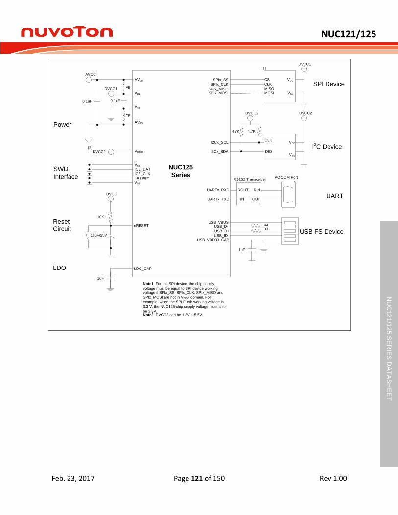
NUC121/125
Feb. 23, 2017 Page 121 of 150 Rev 1.00
NU
C12
1/1
25 S
ER
IES
DA
TA
SH
EE
T
AVSS
AVDD
AVCC
DVCC1
VSS
VDD
0.1uF
FB
FB
DVCC
10uF/25V
10K
Power
Reset
CircuitnRESET
LDO_CAP
NUC125
Series
VDD
VSS
nRESET
ICE_DAT
ICE_CLKSWD
Interface
1uF
VDD
VSS
I2C Device
CLK
DIOI2Cx_SDA
I2Cx_SCL
4.7K
VDD
VSS
SPI DeviceCS
CLK
MISO
SPIx_SS
MOSI
SPIx_CLK
SPIx_MISOSPIx_MOSI
LDO
RS232 Transceiver
ROUT
TIN
RIN
TOUT
PC COM Port
0.1uF
DVCC2
4.7K
DVCC2
DVCC1
Note1: For the SPI device, the chip supply
voltage must be equal to SPI device working
voltage if SPIx_SS, SPIx_CLK, SPIx_MISO and
SPIx_MOSI are not in VDDIO domain. For
example, when the SPI Flash working voltage is
3.3 V, the NUC125 chip supply voltage must also
be 3.3V.
UART
[1]
UARTx_RXD
UARTx_TXD
USB FS DeviceUSB_VDD33_CAP
1uF
USB_D-
USB_D+
USB_ID
USB_VBUS3333
VDDIODVCC2[2]
Note2: DVCC2 can be 1.8V ~ 5.5V.
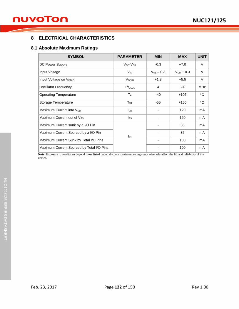
NUC121/125
Feb. 23, 2017 Page 122 of 150 Rev 1.00
NU
C12
1/1
25 S
ER
IES
DA
TA
SH
EE
T
8 ELECTRICAL CHARACTERISTICS
Absolute Maximum Ratings 8.1
SYMBOL PARAMETER MIN MAX UNIT
DC Power Supply VDD-VSS -0.3 +7.0 V
Input Voltage VIN VSS – 0.3 VDD + 0.3 V
Input Voltage on VDDIO VDDIO +1.8 +5.5 V
Oscillator Frequency 1/tCLCL 4 24 MHz
Operating Temperature TA -40 +105 C
Storage Temperature TST -55 +150 C
Maximum Current into VDD IDD - 120 mA
Maximum Current out of VSS ISS - 120 mA
Maximum Current sunk by a I/O Pin
IIO
- 35 mA
Maximum Current Sourced by a I/O Pin - 35 mA
Maximum Current Sunk by Total I/O Pins - 100 mA
Maximum Current Sourced by Total I/O Pins - 100 mA
Note: Exposure to conditions beyond those listed under absolute maximum ratings may adversely affect the lift and reliability of the
device.
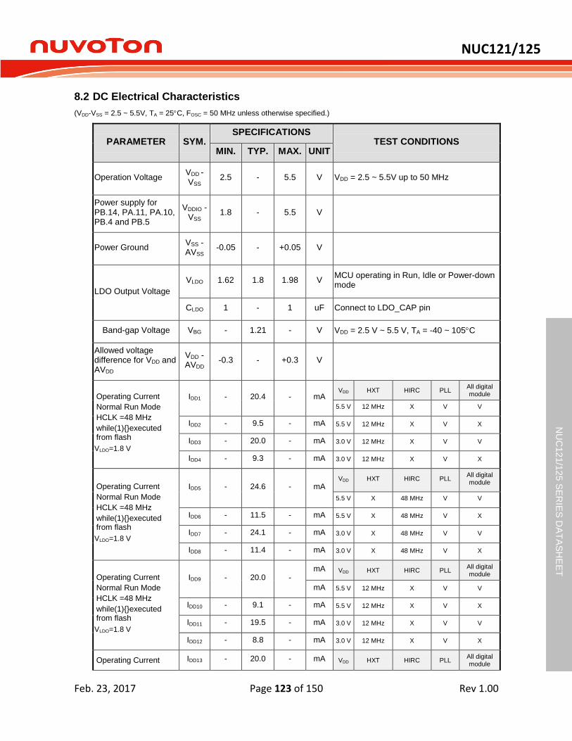
NUC121/125
Feb. 23, 2017 Page 123 of 150 Rev 1.00
NU
C12
1/1
25 S
ER
IES
DA
TA
SH
EE
T
DC Electrical Characteristics 8.2
(VDD-VSS = 2.5 ~ 5.5V, TA = 25C, FOSC = 50 MHz unless otherwise specified.)
PARAMETER SYM. SPECIFICATIONS
TEST CONDITIONS MIN. TYP. MAX. UNIT
Operation Voltage VDD -VSS
2.5 - 5.5 V VDD = 2.5 ~ 5.5V up to 50 MHz
Power supply for PB.14, PA.11, PA.10, PB.4 and PB.5
VDDIO - VSS
1.8 - 5.5 V
Power Ground VSS - AVSS
-0.05 - +0.05 V
LDO Output Voltage
VLDO 1.62 1.8 1.98 V MCU operating in Run, Idle or Power-down mode
CLDO 1 - 1 uF Connect to LDO_CAP pin
Band-gap Voltage VBG - 1.21 - V VDD = 2.5 V ~ 5.5 V, TA = -40 ~ 105C
Allowed voltage difference for VDD and AVDD
VDD - AVDD
-0.3 - +0.3 V
Operating Current
Normal Run Mode
HCLK =48 MHz
while(1){}executed from flash
VLDO=1.8 V
IDD1 - 20.4 - mA VDD HXT HIRC PLL
All digital module
5.5 V 12 MHz X V V
IDD2 - 9.5 - mA 5.5 V 12 MHz X V X
IDD3 - 20.0 - mA 3.0 V 12 MHz X V V
IDD4 - 9.3 - mA 3.0 V 12 MHz X V X
Operating Current
Normal Run Mode
HCLK =48 MHz
while(1){}executed from flash
VLDO=1.8 V
IDD5 - 24.6 - mA VDD HXT HIRC PLL
All digital module
5.5 V X 48 MHz V V
IDD6 - 11.5 - mA 5.5 V X 48 MHz V X
IDD7 - 24.1 - mA 3.0 V X 48 MHz V V
IDD8 - 11.4 - mA 3.0 V X 48 MHz V X
Operating Current
Normal Run Mode
HCLK =48 MHz
while(1){}executed from flash
VLDO=1.8 V
IDD9 - 20.0 - mA VDD HXT HIRC PLL
All digital module
mA 5.5 V 12 MHz X V V
IDD10 - 9.1 - mA 5.5 V 12 MHz X V X
IDD11 - 19.5 - mA 3.0 V 12 MHz X V V
IDD12 - 8.8 - mA 3.0 V 12 MHz X V X
Operating Current IDD13 - 20.0 - mA VDD HXT HIRC PLL All digital module
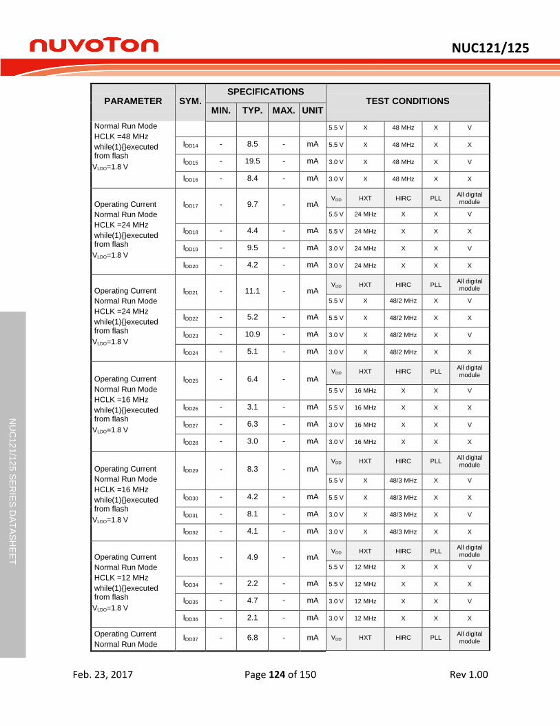
NUC121/125
Feb. 23, 2017 Page 124 of 150 Rev 1.00
NU
C12
1/1
25 S
ER
IES
DA
TA
SH
EE
T
PARAMETER SYM. SPECIFICATIONS
TEST CONDITIONS MIN. TYP. MAX. UNIT
Normal Run Mode
HCLK =48 MHz
while(1){}executed from flash
VLDO=1.8 V
5.5 V X 48 MHz X V
IDD14 - 8.5 - mA 5.5 V X 48 MHz X X
IDD15 - 19.5 - mA 3.0 V X 48 MHz X V
IDD16 - 8.4 - mA 3.0 V X 48 MHz X X
Operating Current
Normal Run Mode
HCLK =24 MHz
while(1){}executed from flash
VLDO=1.8 V
IDD17 - 9.7 - mA VDD HXT HIRC PLL
All digital module
5.5 V 24 MHz X X V
IDD18 - 4.4 - mA 5.5 V 24 MHz X X X
IDD19 - 9.5 - mA 3.0 V 24 MHz X X V
IDD20 - 4.2 - mA 3.0 V 24 MHz X X X
Operating Current
Normal Run Mode
HCLK =24 MHz
while(1){}executed from flash
VLDO=1.8 V
IDD21 - 11.1 - mA VDD HXT HIRC PLL
All digital module
5.5 V X 48/2 MHz X V
IDD22 - 5.2 - mA 5.5 V X 48/2 MHz X X
IDD23 - 10.9 - mA 3.0 V X 48/2 MHz X V
IDD24 - 5.1 - mA 3.0 V X 48/2 MHz X X
Operating Current
Normal Run Mode
HCLK =16 MHz
while(1){}executed from flash
VLDO=1.8 V
IDD25 - 6.4 - mA VDD HXT HIRC PLL
All digital module
5.5 V 16 MHz X X V
IDD26 - 3.1 - mA 5.5 V 16 MHz X X X
IDD27 - 6.3 - mA 3.0 V 16 MHz X X V
IDD28 - 3.0 - mA 3.0 V 16 MHz X X X
Operating Current
Normal Run Mode
HCLK =16 MHz
while(1){}executed from flash
VLDO=1.8 V
IDD29 - 8.3 - mA VDD HXT HIRC PLL
All digital module
5.5 V X 48/3 MHz X V
IDD30 - 4.2 - mA 5.5 V X 48/3 MHz X X
IDD31 - 8.1 - mA 3.0 V X 48/3 MHz X V
IDD32 - 4.1 - mA 3.0 V X 48/3 MHz X X
Operating Current
Normal Run Mode
HCLK =12 MHz
while(1){}executed from flash
VLDO=1.8 V
IDD33 - 4.9 - mA VDD HXT HIRC PLL
All digital module
5.5 V 12 MHz X X V
IDD34 - 2.2 - mA 5.5 V 12 MHz X X X
IDD35 - 4.7 - mA 3.0 V 12 MHz X X V
IDD36 - 2.1 - mA 3.0 V 12 MHz X X X
Operating Current
Normal Run Mode IDD37 - 6.8 - mA VDD HXT HIRC PLL
All digital module
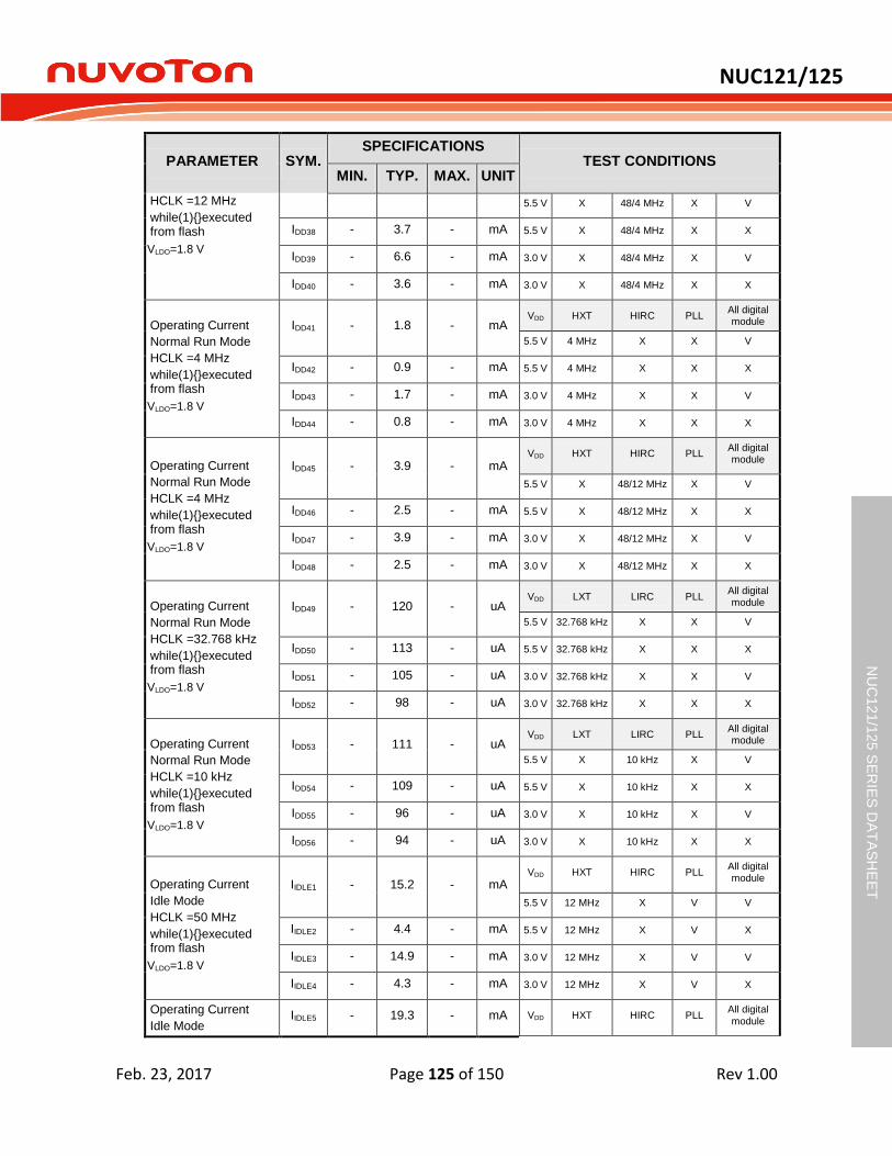
NUC121/125
Feb. 23, 2017 Page 125 of 150 Rev 1.00
NU
C12
1/1
25 S
ER
IES
DA
TA
SH
EE
T
PARAMETER SYM. SPECIFICATIONS
TEST CONDITIONS MIN. TYP. MAX. UNIT
HCLK =12 MHz
while(1){}executed from flash
VLDO=1.8 V
5.5 V X 48/4 MHz X V
IDD38 - 3.7 - mA 5.5 V X 48/4 MHz X X
IDD39 - 6.6 - mA 3.0 V X 48/4 MHz X V
IDD40 - 3.6 - mA 3.0 V X 48/4 MHz X X
Operating Current
Normal Run Mode
HCLK =4 MHz
while(1){}executed from flash
VLDO=1.8 V
IDD41 - 1.8 - mA VDD HXT HIRC PLL
All digital module
5.5 V 4 MHz X X V
IDD42 - 0.9 - mA 5.5 V 4 MHz X X X
IDD43 - 1.7 - mA 3.0 V 4 MHz X X V
IDD44 - 0.8 - mA 3.0 V 4 MHz X X X
Operating Current
Normal Run Mode
HCLK =4 MHz
while(1){}executed from flash
VLDO=1.8 V
IDD45 - 3.9 - mA VDD HXT HIRC PLL
All digital module
5.5 V X 48/12 MHz X V
IDD46 - 2.5 - mA 5.5 V X 48/12 MHz X X
IDD47 - 3.9 - mA 3.0 V X 48/12 MHz X V
IDD48 - 2.5 - mA 3.0 V X 48/12 MHz X X
Operating Current
Normal Run Mode
HCLK =32.768 kHz
while(1){}executed from flash
VLDO=1.8 V
IDD49 - 120 - uA VDD LXT LIRC PLL
All digital module
5.5 V 32.768 kHz X X V
IDD50 - 113 - uA 5.5 V 32.768 kHz X X X
IDD51 - 105 - uA 3.0 V 32.768 kHz X X V
IDD52 - 98 - uA 3.0 V 32.768 kHz X X X
Operating Current
Normal Run Mode
HCLK =10 kHz
while(1){}executed from flash
VLDO=1.8 V
IDD53 - 111 - uA VDD LXT LIRC PLL
All digital module
5.5 V X 10 kHz X V
IDD54 - 109 - uA 5.5 V X 10 kHz X X
IDD55 - 96 - uA 3.0 V X 10 kHz X V
IDD56 - 94 - uA 3.0 V X 10 kHz X X
Operating Current
Idle Mode
HCLK =50 MHz
while(1){}executed from flash
VLDO=1.8 V
IIDLE1 - 15.2 - mA VDD HXT HIRC PLL
All digital module
5.5 V 12 MHz X V V
IIDLE2 - 4.4 - mA 5.5 V 12 MHz X V X
IIDLE3 - 14.9 - mA 3.0 V 12 MHz X V V
IIDLE4 - 4.3 - mA 3.0 V 12 MHz X V X
Operating Current
Idle Mode IIDLE5 - 19.3 - mA VDD HXT HIRC PLL
All digital module
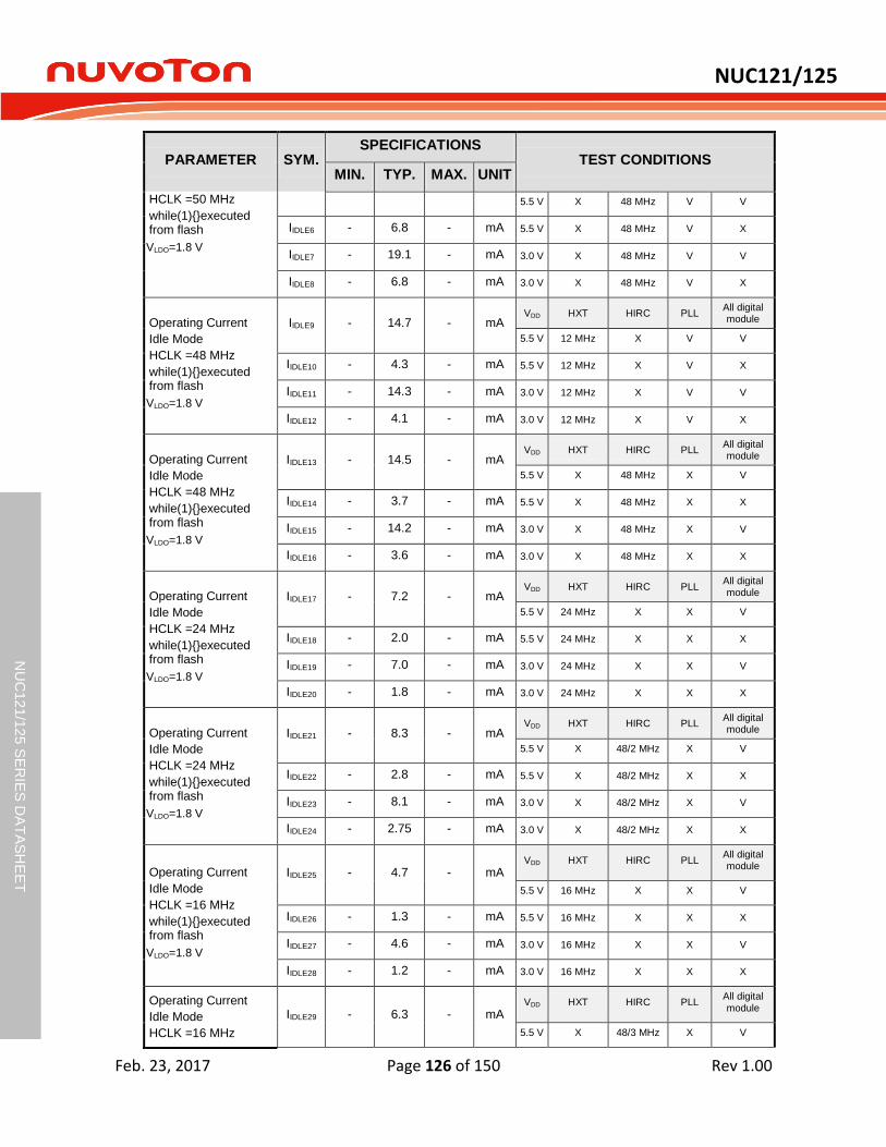
NUC121/125
Feb. 23, 2017 Page 126 of 150 Rev 1.00
NU
C12
1/1
25 S
ER
IES
DA
TA
SH
EE
T
PARAMETER SYM. SPECIFICATIONS
TEST CONDITIONS MIN. TYP. MAX. UNIT
HCLK =50 MHz
while(1){}executed from flash
VLDO=1.8 V
5.5 V X 48 MHz V V
IIDLE6 - 6.8 - mA 5.5 V X 48 MHz V X
IIDLE7 - 19.1 - mA 3.0 V X 48 MHz V V
IIDLE8 - 6.8 - mA 3.0 V X 48 MHz V X
Operating Current
Idle Mode
HCLK =48 MHz
while(1){}executed from flash
VLDO=1.8 V
IIDLE9 - 14.7 - mA VDD HXT HIRC PLL
All digital module
5.5 V 12 MHz X V V
IIDLE10 - 4.3 - mA 5.5 V 12 MHz X V X
IIDLE11 - 14.3 - mA 3.0 V 12 MHz X V V
IIDLE12 - 4.1 - mA 3.0 V 12 MHz X V X
Operating Current
Idle Mode
HCLK =48 MHz
while(1){}executed from flash
VLDO=1.8 V
IIDLE13 - 14.5 - mA VDD HXT HIRC PLL
All digital module
5.5 V X 48 MHz X V
IIDLE14 - 3.7 - mA 5.5 V X 48 MHz X X
IIDLE15 - 14.2 - mA 3.0 V X 48 MHz X V
IIDLE16 - 3.6 - mA 3.0 V X 48 MHz X X
Operating Current
Idle Mode
HCLK =24 MHz
while(1){}executed from flash
VLDO=1.8 V
IIDLE17 - 7.2 - mA VDD HXT HIRC PLL
All digital module
5.5 V 24 MHz X X V
IIDLE18 - 2.0 - mA 5.5 V 24 MHz X X X
IIDLE19 - 7.0 - mA 3.0 V 24 MHz X X V
IIDLE20 - 1.8 - mA 3.0 V 24 MHz X X X
Operating Current
Idle Mode
HCLK =24 MHz
while(1){}executed from flash
VLDO=1.8 V
IIDLE21 - 8.3 - mA VDD HXT HIRC PLL
All digital module
5.5 V X 48/2 MHz X V
IIDLE22 - 2.8 - mA 5.5 V X 48/2 MHz X X
IIDLE23 - 8.1 - mA 3.0 V X 48/2 MHz X V
IIDLE24 - 2.75 - mA 3.0 V X 48/2 MHz X X
Operating Current
Idle Mode
HCLK =16 MHz
while(1){}executed from flash
VLDO=1.8 V
IIDLE25 - 4.7 - mA VDD HXT HIRC PLL
All digital module
5.5 V 16 MHz X X V
IIDLE26 - 1.3 - mA 5.5 V 16 MHz X X X
IIDLE27 - 4.6 - mA 3.0 V 16 MHz X X V
IIDLE28 - 1.2 - mA 3.0 V 16 MHz X X X
Operating Current
Idle Mode
HCLK =16 MHz
IIDLE29 - 6.3 - mA VDD HXT HIRC PLL
All digital module
5.5 V X 48/3 MHz X V

NUC121/125
Feb. 23, 2017 Page 127 of 150 Rev 1.00
NU
C12
1/1
25 S
ER
IES
DA
TA
SH
EE
T
PARAMETER SYM. SPECIFICATIONS
TEST CONDITIONS MIN. TYP. MAX. UNIT
while(1){}executed from flash
VLDO=1.8 V
IIDLE30 - 2.6 - mA 5.5 V X 48/3 MHz X X
IIDLE31 - 6.1 - mA 3.0 V X 48/3 MHz X V
IIDLE32 - 2.5 - mA 3.0 V X 48/3 MHz X X
Operating Current
Idle Mode
HCLK =12 MHz
while(1){}executed from flash
VLDO=1.8 V
IIDLE33 - 3.6 - mA VDD HXT HIRC PLL
All digital module
5.5 V 12 MHz X X V
IIDLE34 - 1.0 - mA 5.5 V 12 MHz X X X
IIDLE35 - 3.5 - mA 3.0 V 12 MHz X X V
IIDLE36 - 0.9 - mA 3.0 V 12 MHz X X X
Operating Current
Idle Mode
HCLK =12 MHz
while(1){}executed from flash
VLDO=1.8 V
IIDLE37 - 5.2 - mA VDD HXT HIRC PLL
All digital module
5.5 V X 48/4 MHz X V
IIDLE38 - 2.4 - mA 5.5 V X 48/4 MHz X X
IIDLE39 - 5.1 - mA 3.0 V X 48/4 MHz X V
IIDLE40 - 2.4 - mA 3.0 V X 48/4 MHz X X
Operating Current
Idle Mode
HCLK =4 MHz
while(1){}executed from flash
VLDO=1.8 V
IIDLE41 - 1.35 - mA VDD HXT HIRC PLL
All digital module
5.5 V 4 MHz X X V
IIDLE42 - 0.48 - mA 5.5 V 4 MHz X X X
IIDLE43 - 1.28 - mA 3.0 V 4 MHz X X V
IIDLE44 - 0.43 - mA 3.0 V 4 MHz X X X
Operating Current
Idle Mode
HCLK =4 MHz
while(1){}executed from flash
VLDO=1.8 V
IIDLE45 - 3.2 - mA VDD HXT HIRC PLL
All digital module
5.5 V X 48/12 MHz X V
IIDLE46 - 2.2 - mA 5.5 V X 48/12 MHz X X
IIDLE47 - 3.1 - mA 3.0 V X 48/12 MHz X V
IIDLE48 - 2.1 - mA 3.0 V X 48/12 MHz X X
Operating Current
Idle Mode
HCLK =32.768 kHz
while(1){}executed from flash
VLDO=1.8 V
IIDLE49 - 116 - uA VDD LXT LIRC PLL
All digital module
5.5 V 32.768 kHz X X V
IIDLE50 - 110 - uA 5.5 V 32.768 kHz X X X
IIDLE51 - 101 - uA 3.0 V 32.768 kHz X X V
IIDLE52 - 95 - uA 3.0 V 32.768 kHz X X X
Operating Current
Idle Mode
HCLK =10 kHz
while(1){}executed from flash
IIDLE53 - 109 - uA VDD LXT LIRC PLL
All digital module
5.5 V X 10 kHz X V
IIDLE54 - 107 - uA 5.5 V X 10 kHz X X
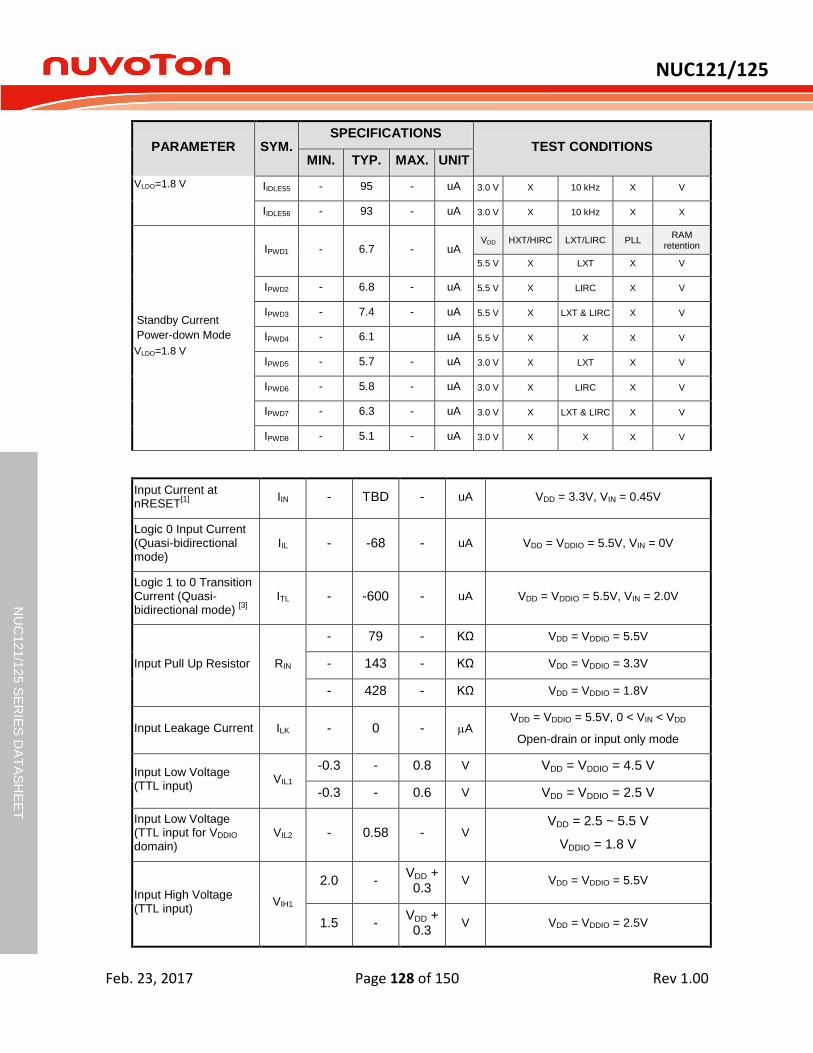
NUC121/125
Feb. 23, 2017 Page 128 of 150 Rev 1.00
NU
C12
1/1
25 S
ER
IES
DA
TA
SH
EE
T
PARAMETER SYM. SPECIFICATIONS
TEST CONDITIONS MIN. TYP. MAX. UNIT
VLDO=1.8 V IIDLE55 - 95 - uA 3.0 V X 10 kHz X V
IIDLE56 - 93 - uA 3.0 V X 10 kHz X X
Standby Current
Power-down Mode
VLDO=1.8 V
IPWD1 - 6.7 - uA VDD HXT/HIRC LXT/LIRC PLL
RAM retention
5.5 V X LXT X V
IPWD2 - 6.8 - uA 5.5 V X LIRC X V
IPWD3 - 7.4 - uA 5.5 V X LXT & LIRC X V
IPWD4 - 6.1 uA 5.5 V X X X V
IPWD5 - 5.7 - uA 3.0 V X LXT X V
IPWD6 - 5.8 - uA 3.0 V X LIRC X V
IPWD7 - 6.3 - uA 3.0 V X LXT & LIRC X V
IPWD8 - 5.1 - uA 3.0 V X X X V
Input Current at nRESET
[1]
IIN - TBD - uA VDD = 3.3V, VIN = 0.45V
Logic 0 Input Current (Quasi-bidirectional mode)
IIL - -68 - uA VDD = VDDIO = 5.5V, VIN = 0V
Logic 1 to 0 Transition Current (Quasi-bidirectional mode)
[3]
ITL - -600 - uA VDD = VDDIO = 5.5V, VIN = 2.0V
Input Pull Up Resistor RIN
- 79 - KΩ VDD = VDDIO = 5.5V
- 143 - KΩ VDD = VDDIO = 3.3V
- 428 - KΩ VDD = VDDIO = 1.8V
Input Leakage Current ILK - 0 - A VDD = VDDIO = 5.5V, 0 < VIN < VDD
Open-drain or input only mode
Input Low Voltage (TTL input)
VIL1 -0.3 - 0.8 V VDD = VDDIO = 4.5 V
-0.3 - 0.6 V VDD = VDDIO = 2.5 V
Input Low Voltage (TTL input for VDDIO domain)
VIL2 - 0.58 - V VDD = 2.5 ~ 5.5 V
VDDIO = 1.8 V
Input High Voltage (TTL input)
VIH1
2.0 - VDD + 0.3
V VDD = VDDIO = 5.5V
1.5 - VDD + 0.3
V VDD = VDDIO = 2.5V
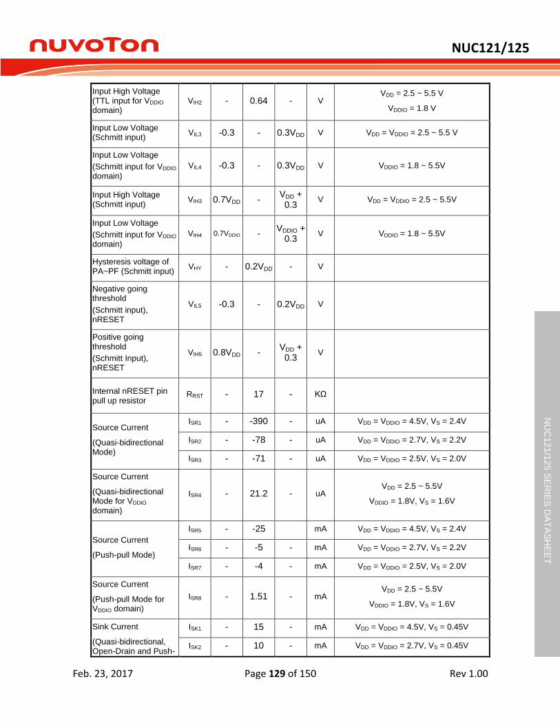
NUC121/125
Feb. 23, 2017 Page 129 of 150 Rev 1.00
NU
C12
1/1
25 S
ER
IES
DA
TA
SH
EE
T
Input High Voltage (TTL input for VDDIO domain)
VIH2 - 0.64 - V VDD = 2.5 ~ 5.5 V
VDDIO = 1.8 V
Input Low Voltage (Schmitt input)
VIL3 -0.3 - 0.3VDD V VDD = VDDIO = 2.5 ~ 5.5 V
Input Low Voltage
(Schmitt input for VDDIO domain)
VIL4 -0.3 - 0.3VDD V VDDIO = 1.8 ~ 5.5V
Input High Voltage (Schmitt input)
VIH3 0.7VDD - VDD + 0.3
V VDD = VDDIO = 2.5 ~ 5.5V
Input Low Voltage
(Schmitt input for VDDIO domain)
VIH4 0.7VDDIO - VDDIO +
0.3 V VDDIO = 1.8 ~ 5.5V
Hysteresis voltage of PA~PF (Schmitt input)
VHY - 0.2VDD - V
Negative going threshold
(Schmitt input), nRESET
VIL5 -0.3 - 0.2VDD V
Positive going threshold
(Schmitt Input), nRESET
VIH5 0.8VDD - VDD + 0.3
V
Internal nRESET pin pull up resistor
RRST - 17 - KΩ
Source Current
(Quasi-bidirectional Mode)
ISR1 - -390 - uA VDD = VDDIO = 4.5V, VS = 2.4V
ISR2 - -78 - uA VDD = VDDIO = 2.7V, VS = 2.2V
ISR3 - -71 - uA VDD = VDDIO = 2.5V, VS = 2.0V
Source Current
(Quasi-bidirectional Mode for VDDIO domain)
ISR4 - 21.2 - uA VDD = 2.5 ~ 5.5V
VDDIO = 1.8V, VS = 1.6V
Source Current
(Push-pull Mode)
ISR5 - -25 mA VDD = VDDIO = 4.5V, VS = 2.4V
ISR6 - -5 - mA VDD = VDDIO = 2.7V, VS = 2.2V
ISR7 - -4 - mA VDD = VDDIO = 2.5V, VS = 2.0V
Source Current
(Push-pull Mode for VDDIO domain)
ISR8 - 1.51 - mA VDD = 2.5 ~ 5.5V
VDDIO = 1.8V, VS = 1.6V
Sink Current
(Quasi-bidirectional, Open-Drain and Push-
ISK1 - 15 - mA VDD = VDDIO = 4.5V, VS = 0.45V
ISK2 - 10 - mA VDD = VDDIO = 2.7V, VS = 0.45V
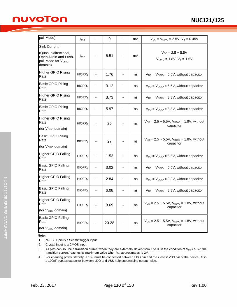
NUC121/125
Feb. 23, 2017 Page 130 of 150 Rev 1.00
NU
C12
1/1
25 S
ER
IES
DA
TA
SH
EE
T
pull Mode) ISK3 - 9 - mA VDD = VDDIO = 2.5V, VS = 0.45V
Sink Current
(Quasi-bidirectional, Open-Drain and Push-pull Mode for VDDIO domain)
ISK4 - 6.51 - mA VDD = 2.5 ~ 5.5V
VDDIO = 1.8V, VS = 1.6V
Higher GPIO Rising Rate
HIORR1 - 1.76 - ns VDD = VDDIO = 5.5V, without capacitor
Basic GPIO Rising Rate
BIORR1 - 3.12 - ns VDD = VDDIO = 5.5V, without capacitor
Higher GPIO Rising Rate
HIORR2 - 3.73 - ns VDD = VDDIO = 3.3V, without capacitor
Basic GPIO Rising Rate
BIORR2 - 5.97 - ns VDD = VDDIO = 3.3V, without capacitor
Higher GPIO Rising Rate
(for VDDIO domain)
HIORR3 - 25 - ns VDD = 2.5 ~ 5.5V, VDDIO = 1.8V, without
capacitor
Basic GPIO Rising Rate
(for VDDIO domain)
BIORR3 - 27 - ns VDD = 2.5 ~ 5.5V, VDDIO = 1.8V, without
capacitor
Higher GPIO Falling Rate
HIOFR1 - 1.53 - ns VDD = VDDIO = 5.5V, without capacitor
Basic GPIO Falling Rate
BIOFR1 - 3.02 - ns VDD = VDDIO = 5.5V, without capacitor
Higher GPIO Falling Rate
HIOFR2 - 2.84 - ns VDD = VDDIO = 3.3V, without capacitor
Basic GPIO Falling Rate
BIOFR2 - 6.08 - ns VDD = VDDIO = 3.3V, without capacitor
Higher GPIO Falling Rate
(for VDDIO domain)
HIOFR3 - 8.69 - ns VDD = 2.5 ~ 5.5V, VDDIO = 1.8V, without
capacitor
Basic GPIO Falling Rate
(for VDDIO domain)
BIOFR3 - 20.28 - ns VDD = 2.5 ~ 5.5V, VDDIO = 1.8V, without
capacitor
Note:
1. nRESET pin is a Schmitt trigger input.
2. Crystal Input is a CMOS input.
3. All pins can source a transition current when they are externally driven from 1 to 0. In the condition of VDD = 5.5V, the transition current reaches its maximum value when VIN approximates to 2V.
4. For ensuring power stability, a 1uF must be connected between LDO pin and the closest VSS pin of the device. Also a 100nF bypass capacitor between LDO and VSS help suppressing output noise.
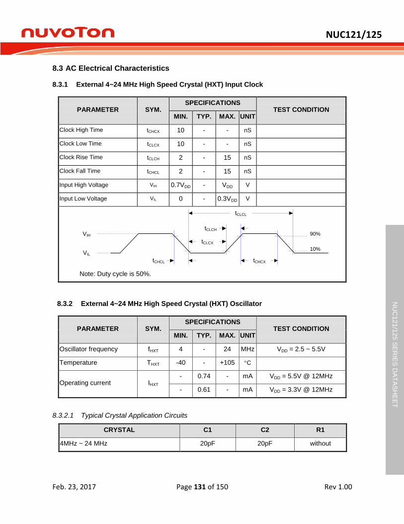
NUC121/125
Feb. 23, 2017 Page 131 of 150 Rev 1.00
NU
C12
1/1
25 S
ER
IES
DA
TA
SH
EE
T
AC Electrical Characteristics 8.3
8.3.1 External 4~24 MHz High Speed Crystal (HXT) Input Clock
PARAMETER SYM. SPECIFICATIONS
TEST CONDITION MIN. TYP. MAX. UNIT
Clock High Time tCHCX 10 - - nS
Clock Low Time tCLCX 10 - - nS
Clock Rise Time tCLCH 2 - 15 nS
Clock Fall Time tCHCL 2 - 15 nS
Input High Voltage VIH 0.7VDD - VDD V
Input Low Voltage VIL 0 - 0.3VDD V
tCHCX
90%
10%
tCLCH
tCHCL
tCLCX
tCLCL
VIL
VIH
Note: Duty cycle is 50%.
8.3.2 External 4~24 MHz High Speed Crystal (HXT) Oscillator
PARAMETER SYM. SPECIFICATIONS
TEST CONDITION MIN. TYP. MAX. UNIT
Oscillator frequency fHXT 4 - 24 MHz VDD = 2.5 ~ 5.5V
Temperature THXT -40 - +105 C
Operating current IHXT - 0.74 - mA VDD = 5.5V @ 12MHz
- 0.61 - mA VDD = 3.3V @ 12MHz
Typical Crystal Application Circuits 8.3.2.1
CRYSTAL C1 C2 R1
4MHz ~ 24 MHz 20pF 20pF without

NUC121/125
Feb. 23, 2017 Page 132 of 150 Rev 1.00
NU
C12
1/1
25 S
ER
IES
DA
TA
SH
EE
T
XT_INXT_OUT
C1R1C2
Figure 8.3-1 Typical Crystal Application Circuit
8.3.3 External 32.768 kHz Low Speed Crystal (LXT) Input Clock
PARAMETER SYM. SPECIFICATIONS
TEST CONDITION MIN. TYP. MAX. UNIT
Clock High Time tCHCX TBD - - nS
Clock Low Time tCLCX TBD - - nS
Clock Rise Time tCLCH TBD - TBD nS
Clock Fall Time tCHCL TBD - TBD nS
LXT Input Pin Input High Voltage
Xin_VIH 0.7VDD - VDD V
LXT Input Pin Input Low Voltage
Xin_VIL 0 - 0.3VDD V
tCHCX
90%
10%
tCLCH
tCHCL
tCLCX
tCLCL
Xin_VIL
Xin_VIH
Note: Duty cycle is 50%.
8.3.4 External 32.768 kHz Low Speed Crystal (LXT) Oscillator
PARAMETER SYM. SPECIFICATIONS
TEST CONDITION MIN. TYP. MAX. UNIT
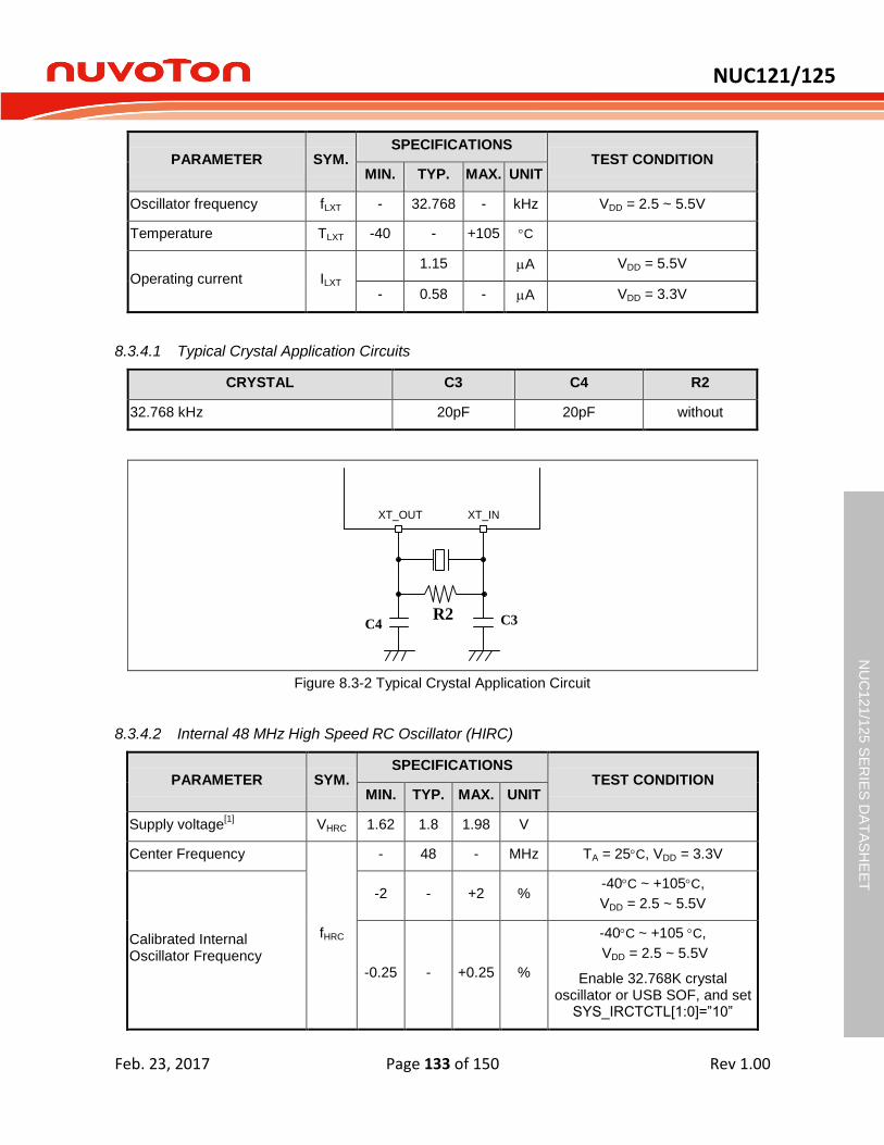
NUC121/125
Feb. 23, 2017 Page 133 of 150 Rev 1.00
NU
C12
1/1
25 S
ER
IES
DA
TA
SH
EE
T
PARAMETER SYM. SPECIFICATIONS
TEST CONDITION MIN. TYP. MAX. UNIT
Oscillator frequency fLXT - 32.768 - kHz VDD = 2.5 ~ 5.5V
Temperature TLXT -40 - +105 C
Operating current ILXT 1.15 A VDD = 5.5V
- 0.58 - A VDD = 3.3V
Typical Crystal Application Circuits 8.3.4.1
CRYSTAL C3 C4 R2
32.768 kHz 20pF 20pF without
XT_INXT_OUT
C3R2C4
Figure 8.3-2 Typical Crystal Application Circuit
Internal 48 MHz High Speed RC Oscillator (HIRC) 8.3.4.2
PARAMETER SYM. SPECIFICATIONS
TEST CONDITION MIN. TYP. MAX. UNIT
Supply voltage[1]
VHRC 1.62 1.8 1.98 V
Center Frequency
fHRC
- 48 - MHz TA = 25C, VDD = 3.3V
Calibrated Internal Oscillator Frequency
-2 - +2 % -40C ~ +105C,
VDD = 2.5 ~ 5.5V
-0.25 - +0.25 %
-40C ~ +105 C,
VDD = 2.5 ~ 5.5V
Enable 32.768K crystal oscillator or USB SOF, and set
SYS_IRCTCTL[1:0]=”10”

NUC121/125
Feb. 23, 2017 Page 134 of 150 Rev 1.00
NU
C12
1/1
25 S
ER
IES
DA
TA
SH
EE
T
PARAMETER SYM. SPECIFICATIONS
TEST CONDITION MIN. TYP. MAX. UNIT
Operating current IHRC - 431 - A VDD = 5.5 V
- 430 - A VDD = 3.3 V
Internal 10 kHz Low Speed RC Oscillator (LIRC) 8.3.4.3
PARAMETER SYM. SPECIFICATIONS
TEST CONDITION MIN. TYP. MAX. UNIT
Supply voltage[1]
VLRC 1.62 1.8 1.98 V
Center Frequency
FLRC
- 10 - kHz 25C, VDD = 3.3V
Calibrated Internal Oscillator Frequency
-30 - +30 % 25 C,
VDD = 2.5 ~ 5.5V
-50 - +50 % -40C ~+105 C,
VDD = 2.5 ~ 5.5V
Operating current ILRC - 0.74 - A VDD = 5.5V
0.66 A VDD = 3.3V
Note: Internal oscillator operation voltage comes from LDO.
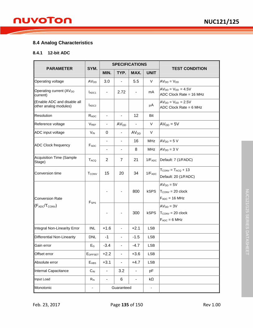
NUC121/125
Feb. 23, 2017 Page 135 of 150 Rev 1.00
NU
C12
1/1
25 S
ER
IES
DA
TA
SH
EE
T
Analog Characteristics 8.4
8.4.1 12-bit ADC
PARAMETER SYM. SPECIFICATIONS
TEST CONDITION MIN. TYP. MAX. UNIT
Operating voltage AVDD 3.0 - 5.5 V AVDD = VDD
Operating current (AVDD current)
(Enable ADC and disable all other analog modules)
IADC1 - 2.72 - mA AVDD = VDD = 4.5V
ADC Clock Rate = 16 MHz
IADC2 A AVDD = VDD = 2.5V
ADC Clock Rate = 6 MHz
Resolution RADC - - 12 Bit
Reference voltage VREF - AVDD - V AVDD = 5V
ADC input voltage VIN 0 - AVDD V
ADC Clock frequency FADC - - 16 MHz AVDD = 5 V
- - 8 MHz AVDD = 3 V
Acquisition Time (Sample Stage)
TACQ 2 7 21 1/FADC Default: 7 (1/FADC)
Conversion time TCONV 15 20 34 1/FADC TCONV = TACQ + 13
Default: 20 (1/FADC)
Conversion Rate
(FADC/TCONV) FSPS
- - 800 kSPS
AVDD = 5V
TCONV = 20 clock
FADC = 16 MHz
- - 300 kSPS
AVDD = 3V
TCONV = 20 clock
FADC = 6 MHz
Integral Non-Linearity Error INL +1.6 - +2.1 LSB
Differential Non-Linearity DNL -1 - -1.5 LSB
Gain error EG -3.4 - -4.7 LSB
Offset error EOFFSET +2.2 - +3.6 LSB
Absolute error EABS +3.1 - +4.7 LSB
Internal Capacitance CIN - 3.2 - pF
Input Load RIN - 6 - kΩ
Monotonic - Guaranteed -
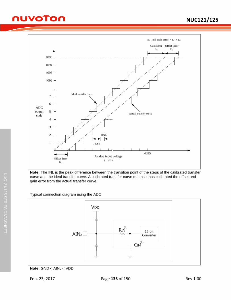
NUC121/125
Feb. 23, 2017 Page 136 of 150 Rev 1.00
NU
C12
1/1
25 S
ER
IES
DA
TA
SH
EE
T
1
2
3
4
5
6
4095
4094
7
4093
4092
Ideal transfer curve
Actual transfer curve
Offset Error
EO
Analog input voltage
(LSB)
4095
ADC
output
code
Offset Error
EO
Gain Error
EG
EF (Full scale error) = EO + EG
DNL
1 LSB
Note: The INL is the peak difference between the transition point of the steps of the calibrated transfer curve and the ideal transfer curve. A calibrated transfer curve means it has calibrated the offset and gain error from the actual transfer curve.
Typical connection diagram using the ADC
VDD
12-bit ConverterAINx
RIN
CIN
(1)
(1)
Note: GND < AINX < VDD
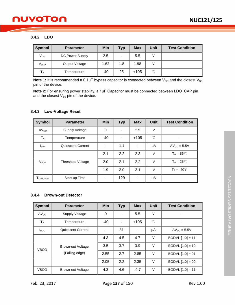
NUC121/125
Feb. 23, 2017 Page 137 of 150 Rev 1.00
NU
C12
1/1
25 S
ER
IES
DA
TA
SH
EE
T
8.4.2 LDO
Symbol Parameter Min Typ Max Unit Test Condition
VDD DC Power Supply 2.5 - 5.5 V
VLDO Output Voltage 1.62 1.8 1.98 V
TA Temperature -40 25 +105 ℃
Note 1: It is recommended a 0.1μF bypass capacitor is connected between VDD and the closest VSS pin of the device.
Note 2: For ensuring power stability, a 1μF Capacitor must be connected between LDO_CAP pin and the closest VSS pin of the device.
8.4.3 Low-Voltage Reset
Symbol Parameter Min Typ Max Unit Test Condition
AVDD Supply Voltage 0 - 5.5 V
TA Temperature -40 - +105 ℃ -
ILVR Quiescent Current - 1.1 - uA AVDD = 5.5V
VPOR Threshold Voltage
2.1 2.2 2.3 V TA = 85℃
2.0 2.1 2.2 V TA = 25℃
1.9 2.0 2.1 V TA = -40℃
TLVR_Start Start-up Time - 129 - uS
8.4.4 Brown-out Detector
Symbol Parameter Min Typ Max Unit Test Condition
AVDD Supply Voltage 0 - 5.5 V -
TA Temperature -40 - +105 ℃ -
IBOD Quiescent Current - 81 - μA AVDD = 5.5V
VBOD Brown-out Voltage
(Falling edge)
4.3 4.5 4.7 V BODVL [1:0] = 11
3.5 3.7 3.9 V BODVL [1:0] = 10
2.55 2.7 2.85 V BODVL [1:0] = 01
2.05 2.2 2.35 V BODVL [1:0] = 00
VBOD Brown-out Voltage 4.3 4.6 .4.7 V BODVL [1:0] = 11
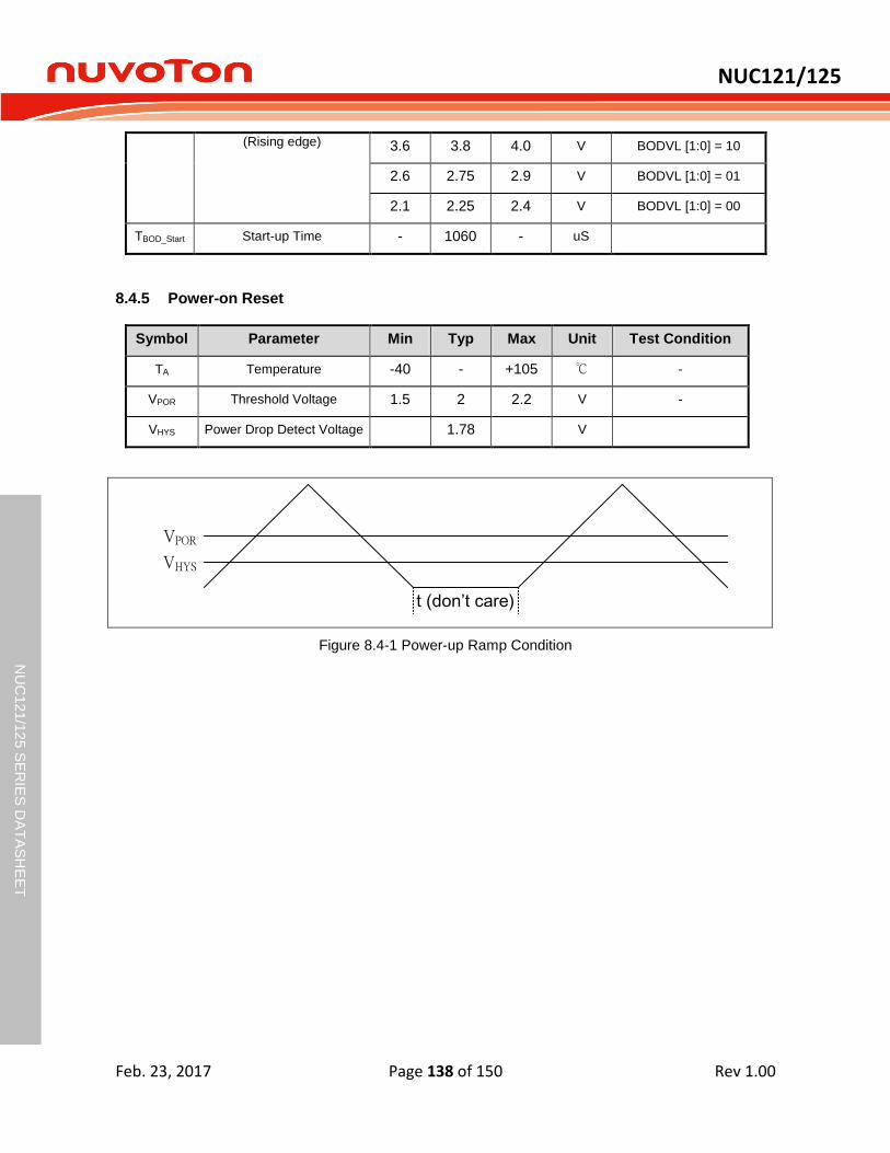
NUC121/125
Feb. 23, 2017 Page 138 of 150 Rev 1.00
NU
C12
1/1
25 S
ER
IES
DA
TA
SH
EE
T
(Rising edge) 3.6 3.8 4.0 V BODVL [1:0] = 10
2.6 2.75 2.9 V BODVL [1:0] = 01
2.1 2.25 2.4 V BODVL [1:0] = 00
TBOD_Start Start-up Time - 1060 - uS
8.4.5 Power-on Reset
Symbol Parameter Min Typ Max Unit Test Condition
TA Temperature -40 - +105 ℃ -
VPOR Threshold Voltage 1.5 2 2.2 V -
VHYS Power Drop Detect Voltage 1.78 V
t (don’t care)
VPOR
VHYS
Figure 8.4-1 Power-up Ramp Condition
NUC121/125
Feb. 23, 2017 Page 139 of 150 Rev 1.00
NU
C12
1/1
25 S
ER
IES
DA
TA
SH
EE
T
8.4.6 Temperature Sensor
PARAMETER SYM. SPECIFICATIONS TEST CONDITION
(supply voltage = 3V) MIN. TYP. MAX. UNIT
Detection Temperature TDET -40 - +105 oC
Operating current ITEMP 6.4 - 10.5 A
Gain VTG -1.8 -1.76 -1.73 mV/ o
C
Offset VTO - 725 - mV Temperature at 0 oC
Note 1: Internal operation voltage comes from LDO.
Note 2: The temperature sensor formula for the output voltage (Vtemp) is as below equation.
Vtemp (mV) = Gain (mV/℃ ) x Temperature (℃) + Offset (mV)
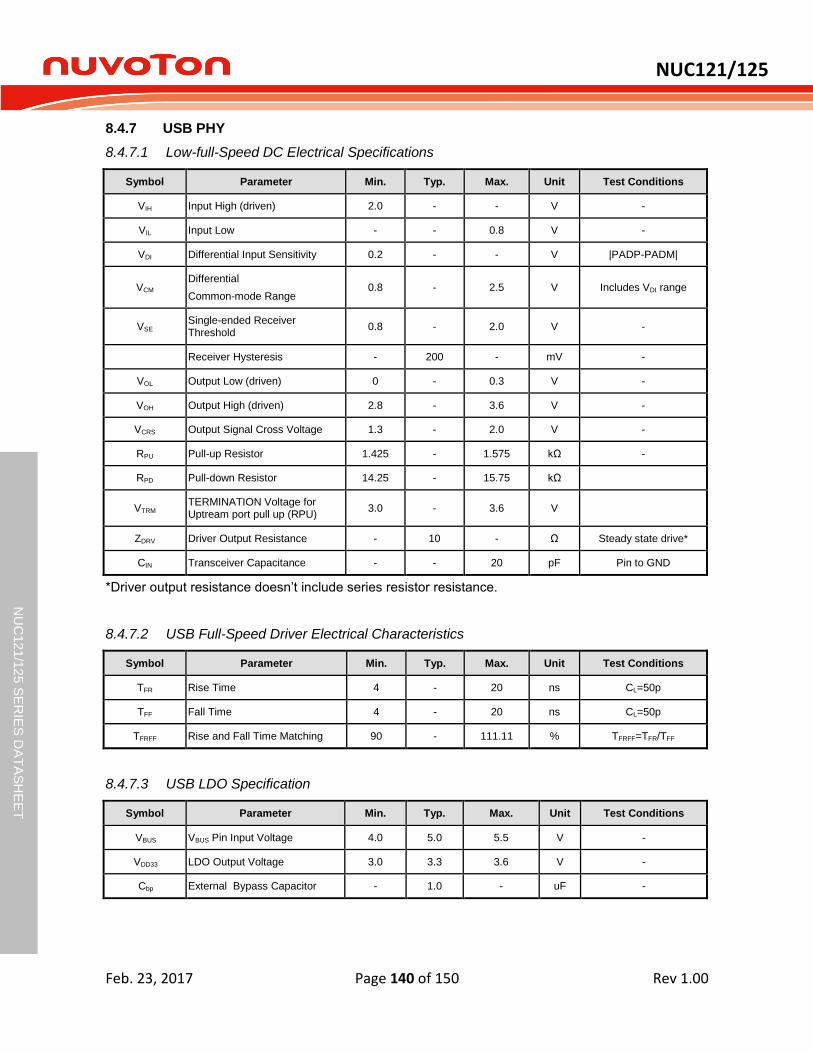
NUC121/125
Feb. 23, 2017 Page 140 of 150 Rev 1.00
NU
C12
1/1
25 S
ER
IES
DA
TA
SH
EE
T
8.4.7 USB PHY
Low-full-Speed DC Electrical Specifications 8.4.7.1
Symbol Parameter Min. Typ. Max. Unit Test Conditions
VIH Input High (driven) 2.0 - - V -
VIL Input Low - - 0.8 V -
VDI Differential Input Sensitivity 0.2 - - V |PADP-PADM|
VCM Differential
Common-mode Range 0.8 - 2.5 V Includes VDI range
VSE Single-ended Receiver Threshold
0.8 - 2.0 V -
Receiver Hysteresis - 200 - mV -
VOL Output Low (driven) 0 - 0.3 V -
VOH Output High (driven) 2.8 - 3.6 V -
VCRS Output Signal Cross Voltage 1.3 - 2.0 V -
RPU Pull-up Resistor 1.425 - 1.575 kΩ -
RPD Pull-down Resistor 14.25 - 15.75 kΩ
VTRM TERMINATION Voltage for Uptream port pull up (RPU)
3.0 - 3.6 V
ZDRV Driver Output Resistance - 10 - Ω Steady state drive*
CIN Transceiver Capacitance - - 20 pF Pin to GND
*Driver output resistance doesn’t include series resistor resistance.
USB Full-Speed Driver Electrical Characteristics 8.4.7.2
Symbol Parameter Min. Typ. Max. Unit Test Conditions
TFR Rise Time 4 - 20 ns CL=50p
TFF Fall Time 4 - 20 ns CL=50p
TFRFF Rise and Fall Time Matching 90 - 111.11 % TFRFF=TFR/TFF
USB LDO Specification 8.4.7.3
Symbol Parameter Min. Typ. Max. Unit Test Conditions
VBUS VBUS Pin Input Voltage 4.0 5.0 5.5 V -
VDD33 LDO Output Voltage 3.0 3.3 3.6 V -
Cbp External Bypass Capacitor - 1.0 - uF -
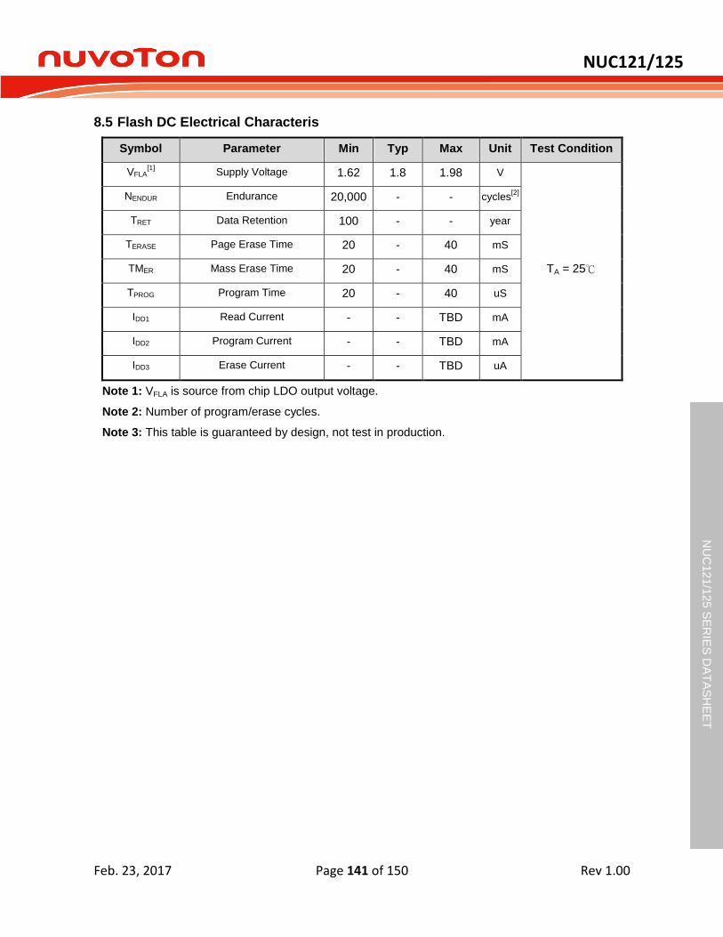
NUC121/125
Feb. 23, 2017 Page 141 of 150 Rev 1.00
NU
C12
1/1
25 S
ER
IES
DA
TA
SH
EE
T
Flash DC Electrical Characteris 8.5
Symbol Parameter Min Typ Max Unit Test Condition
VFLA[1]
Supply Voltage 1.62 1.8 1.98 V
TA = 25℃
NENDUR Endurance 20,000 - - cycles[2]
TRET Data Retention 100 - - year
TERASE Page Erase Time 20 - 40 mS
TMER Mass Erase Time 20 - 40 mS
TPROG Program Time 20 - 40 uS
IDD1 Read Current - - TBD mA
IDD2 Program Current - - TBD mA
IDD3 Erase Current - - TBD uA
Note 1: VFLA is source from chip LDO output voltage.
Note 2: Number of program/erase cycles.
Note 3: This table is guaranteed by design, not test in production.
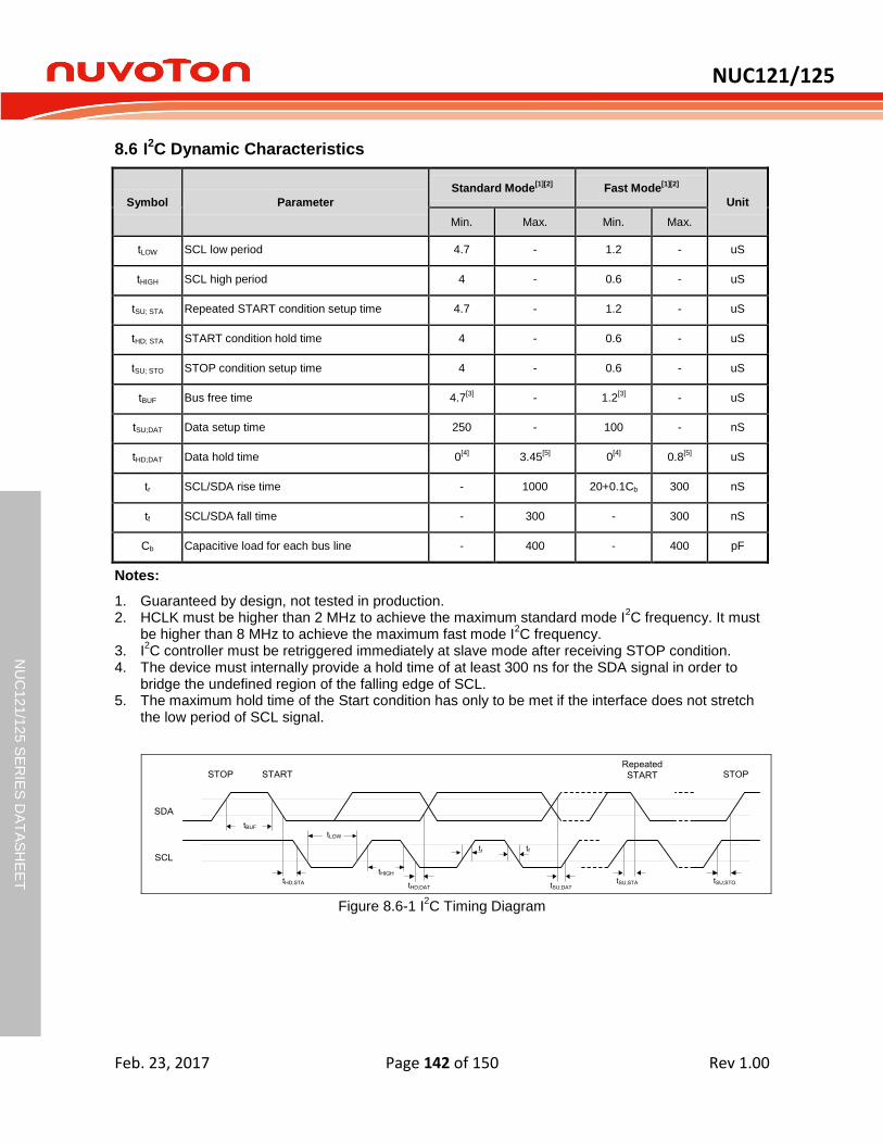
NUC121/125
Feb. 23, 2017 Page 142 of 150 Rev 1.00
NU
C12
1/1
25 S
ER
IES
DA
TA
SH
EE
T
I2C Dynamic Characteristics 8.6
Symbol Parameter
Standard Mode[1][2]
Fast Mode[1][2]
Unit
Min. Max. Min. Max.
tLOW SCL low period 4.7 - 1.2 - uS
tHIGH SCL high period 4 - 0.6 - uS
tSU; STA Repeated START condition setup time 4.7 - 1.2 - uS
tHD; STA START condition hold time 4 - 0.6 - uS
tSU; STO STOP condition setup time 4 - 0.6 - uS
tBUF Bus free time 4.7[3]
- 1.2[3]
- uS
tSU;DAT Data setup time 250 - 100 - nS
tHD;DAT Data hold time 0[4]
3.45[5]
0[4]
0.8[5]
uS
tr SCL/SDA rise time - 1000 20+0.1Cb 300 nS
tf SCL/SDA fall time - 300 - 300 nS
Cb Capacitive load for each bus line - 400 - 400 pF
Notes:
1. Guaranteed by design, not tested in production. 2. HCLK must be higher than 2 MHz to achieve the maximum standard mode I
2C frequency. It must
be higher than 8 MHz to achieve the maximum fast mode I2C frequency.
3. I2C controller must be retriggered immediately at slave mode after receiving STOP condition.
4. The device must internally provide a hold time of at least 300 ns for the SDA signal in order to bridge the undefined region of the falling edge of SCL.
5. The maximum hold time of the Start condition has only to be met if the interface does not stretch the low period of SCL signal.
tBUF
STOP
SDA
SCL
START
tHD;STA
tLOW
tHD;DAT
tHIGH
tf
tSU;DAT
Repeated
START
tSU;STA tSU;STO
STOP
tr
Figure 8.6-1 I
2C Timing Diagram
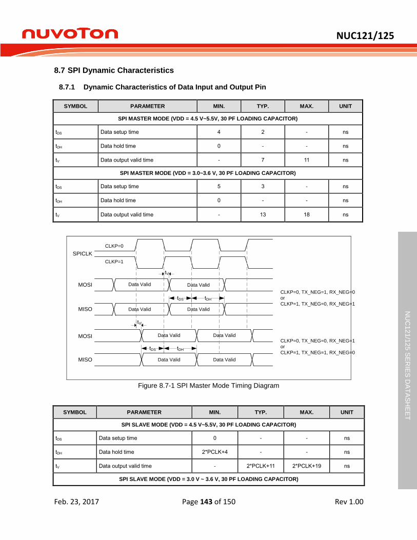
NUC121/125
Feb. 23, 2017 Page 143 of 150 Rev 1.00
NU
C12
1/1
25 S
ER
IES
DA
TA
SH
EE
T
SPI Dynamic Characteristics 8.7
8.7.1 Dynamic Characteristics of Data Input and Output Pin
SYMBOL PARAMETER MIN. TYP. MAX. UNIT
SPI MASTER MODE (VDD = 4.5 V~5.5V, 30 PF LOADING CAPACITOR)
tDS Data setup time 4 2 - ns
tDH Data hold time 0 - - ns
tV Data output valid time - 7 11 ns
SPI MASTER MODE (VDD = 3.0~3.6 V, 30 PF LOADING CAPACITOR)
tDS Data setup time 5 3 - ns
tDH Data hold time 0 - - ns
tV Data output valid time - 13 18 ns
CLKP=0, TX_NEG=1, RX_NEG=0
or
CLKP=1, TX_NEG=0, RX_NEG=1
CLKP=0, TX_NEG=0, RX_NEG=1
or
CLKP=1, TX_NEG=1, RX_NEG=0
MISO
MOSI Data Valid
Data ValidData Valid
Data Valid
SPICLK
MISO
MOSI Data Valid
Data ValidData Valid
Data Valid
CLKP=0
CLKP=1
tV
tDS tDH
tV
tDS tDH
Figure 8.7-1 SPI Master Mode Timing Diagram
SYMBOL PARAMETER MIN. TYP. MAX. UNIT
SPI SLAVE MODE (VDD = 4.5 V~5.5V, 30 PF LOADING CAPACITOR)
tDS Data setup time 0 - - ns
tDH Data hold time 2*PCLK+4 - - ns
tV Data output valid time - 2*PCLK+11 2*PCLK+19 ns
SPI SLAVE MODE (VDD = 3.0 V ~ 3.6 V, 30 PF LOADING CAPACITOR)
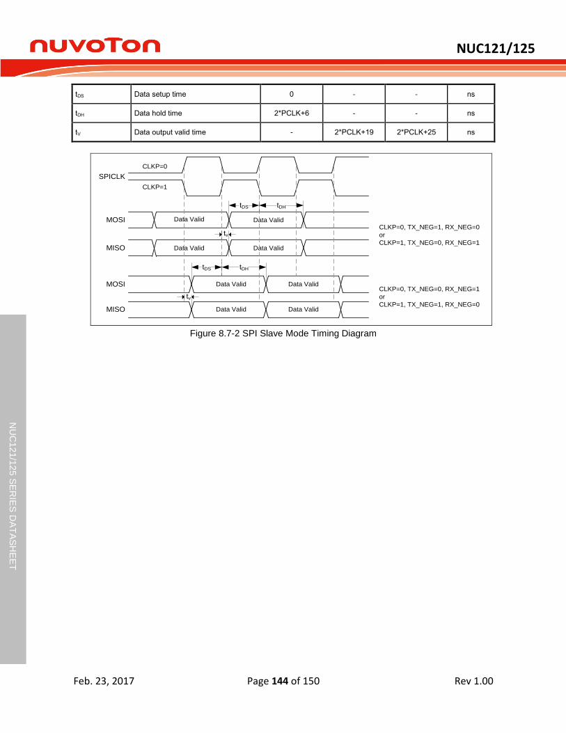
NUC121/125
Feb. 23, 2017 Page 144 of 150 Rev 1.00
NU
C12
1/1
25 S
ER
IES
DA
TA
SH
EE
T
tDS Data setup time 0 - - ns
tDH Data hold time 2*PCLK+6 - - ns
tV Data output valid time - 2*PCLK+19 2*PCLK+25 ns
CLKP=0, TX_NEG=1, RX_NEG=0
or
CLKP=1, TX_NEG=0, RX_NEG=1
CLKP=0, TX_NEG=0, RX_NEG=1
or
CLKP=1, TX_NEG=1, RX_NEG=0MISO
MOSI Data Valid
Data ValidData Valid
Data Valid
SPICLK
MISO
MOSI Data Valid
Data ValidData Valid
Data Valid
CLKP=0
CLKP=1
tv
tDS tDH
tv
tDS tDH
Figure 8.7-2 SPI Slave Mode Timing Diagram
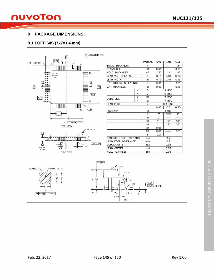
NUC121/125
Feb. 23, 2017 Page 145 of 150 Rev 1.00
NU
C12
1/1
25 S
ER
IES
DA
TA
SH
EE
T
9 PACKAGE DIMENSIONS
LQFP 64S (7x7x1.4 mm) 9.1
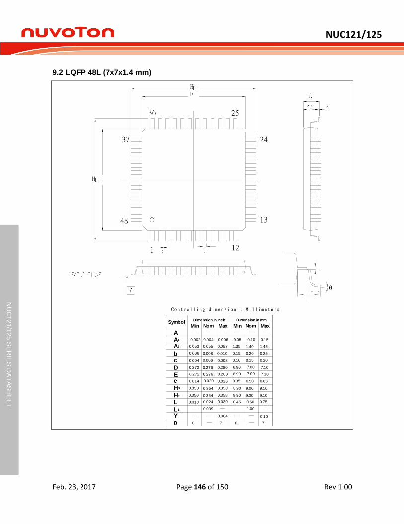
NUC121/125
Feb. 23, 2017 Page 146 of 150 Rev 1.00
NU
C12
1/1
25 S
ER
IES
DA
TA
SH
EE
T
LQFP 48L (7x7x1.4 mm) 9.2
1 12
48
H
H
C o n t r o l l i n g d i me n s i o n : M i l l i m e t e r s
0.10
070
0.004
1.00
0.750.600.45
0.039
0.0300.0240.018
9.109.008.900.3580.3540.350
0.50
0.20
0.25
1.451.40
0.10
0.15
1.35
0.008
0.010
0.0570.055
0.026
7.107.006.900.2800.2760.272
0.004
0.006
0.053
SymbolMin Nom Max MaxNomMin
Dimension in inch Dimension in mm
A
bc
D
e
HD
HE
L
Y
0
AA
L1
1
2
E
0.008
0.006 0.15
0.20
7
0.020 0.35 0.65
0.100.050.002 0.004 0.006 0.15
9.109.008.900.3580.3540.350
7.107.006.900.2800.2760.272
0.014
37
36 25
24
13
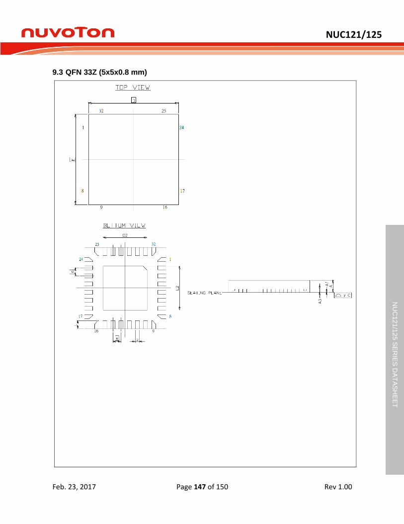
NUC121/125
Feb. 23, 2017 Page 147 of 150 Rev 1.00
NU
C12
1/1
25 S
ER
IES
DA
TA
SH
EE
T
QFN 33Z (5x5x0.8 mm) 9.3
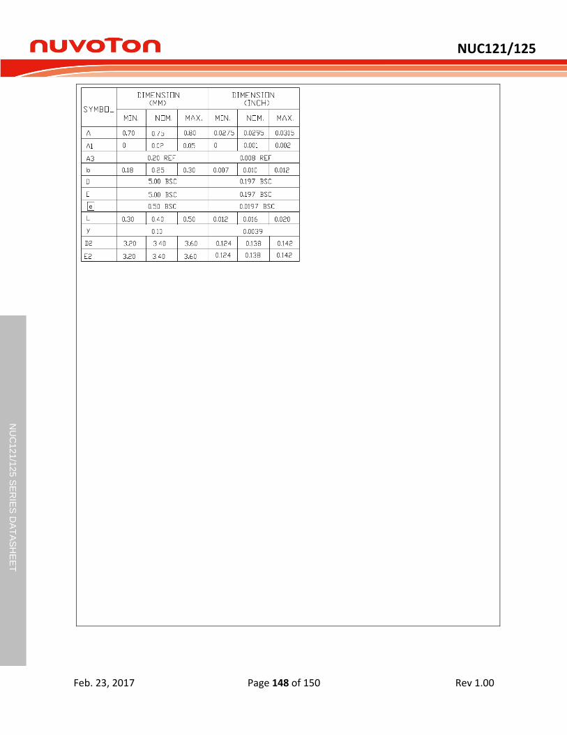
NUC121/125
Feb. 23, 2017 Page 148 of 150 Rev 1.00
NU
C12
1/1
25 S
ER
IES
DA
TA
SH
EE
T
NUC121/125
Feb. 23, 2017 Page 149 of 150 Rev 1.00
NU
C12
1/1
25 S
ER
IES
DA
TA
SH
EE
T
10 REVISION HISTORY
Revision Date Description
1.00 2017.02.15 Preliminary version
NUC121/125
Feb. 23, 2017 Page 150 of 150 Rev 1.00
NU
C12
1/1
25 S
ER
IES
DA
TA
SH
EE
T
Important Notice
Nuvoton Products are neither intended nor warranted for usage in systems or equipment, any malfunction or failure of which may cause loss of human life, bodily injury or severe property damage. Such applications are deemed, “Insecure Usage”.
Insecure usage includes, but is not limited to: equipment for surgical implementation, atomic energy control instruments, airplane or spaceship instruments, the control or operation of dynamic, brake or safety systems designed for vehicular use, traffic signal instruments, all types of safety devices, and other applications intended to support or sustain life.
All Insecure Usage shall be made at customer’s risk, and in the event that third parties lay claims to Nuvoton as a result of customer’s Insecure Usage, customer shall indemnify the damages and liabilities thus incurred by Nuvoton.