NuMicro™ M0518 Series Technical Reference Manual · NuMicro M0518 Series Technical Reference...
497
NuMicro M0518 Series Technical Reference Manual Oct 31, 2014 Page 1 of 497 Revision 1.00 NUMICRO™ M0518 SERIES TECHNICAL REFERENCE MANUAL NuMicro™ M0518 Series Technical Reference Manual The information described in this document is the exclusive intellectual property of Nuvoton Technology Corporation and shall not be reproduced without permission from Nuvoton. Nuvoton is providing this document only for reference purposes of NuMicro TM microcontroller based system design. Nuvoton assumes no responsibility for errors or omissions. All data and specifications are subject to change without notice. For additional information or questions, please contact: Nuvoton Technology Corporation. www.nuvoton.com
Transcript of NuMicro™ M0518 Series Technical Reference Manual · NuMicro M0518 Series Technical Reference...
NuMicro M0518 Series Technical Reference Manual
Oct 31, 2014 Page 1 of 497 Revision 1.00
NU
MIC
RO
™ M
0518
SE
RIE
S T
EC
HN
ICA
L R
EF
ER
EN
CE
MA
NU
AL
NuMicro™ M0518 Series
Technical Reference Manual
The information described in this document is the exclusive intellectual property of Nuvoton Technology Corporation and shall not be reproduced without permission from Nuvoton.
Nuvoton is providing this document only for reference purposes of NuMicroTM
microcontroller based system design. Nuvoton assumes no responsibility for errors or omissions.
All data and specifications are subject to change without notice.
For additional information or questions, please contact: Nuvoton Technology Corporation.
www.nuvoton.com

NuMicro M0518 Series Technical Reference Manual
Oct 31, 2014 Page 2 of 497 Revision 1.00
NU
MIC
RO
™ M
0518
SE
RIE
S T
EC
HN
ICA
L R
EF
ER
EN
CE
MA
NU
AL
TABLE OF CONTENTS
1 GENERAL DESCRIPTION ................................................................................... 12
2 FEATURES .......................................................................................................... 13
3 ABBREVIATIONS ................................................................................................ 16
4 PARTS INFORMATION LIST AND PIN CONFIGURATION ................................ 17
4.1 NuMicro M0518 Series Selection Code .................................................... 17
4.2 NuMicro M0518 Selection Guide ............................................................ 18
4.3 Pin Configuration ................................................................................. 19
4.3.1 NuMicro M0518 Pin Diagram ...................................................................... 19
4.4 Pin Description .................................................................................... 21
4.4.1 NuMicro M0518 Pin Description .................................................................. 21
5 BLOCK DIAGRAM ............................................................................................... 27
5.1 NuMicro M0518 Block Diagram .............................................................. 27
6 FUNCTIONAL DESCRIPTION ............................................................................. 28
6.1 ARM® Cortex™-M0 Core ....................................................................... 28
6.2 System Manager ................................................................................. 30
6.2.1 Overview ................................................................................................ 30
6.2.2 System Reset .......................................................................................... 30
6.2.3 System Power Distribution ........................................................................... 31
6.2.4 System Memory Map ................................................................................. 32
6.2.5 Register Map ........................................................................................... 34
6.2.6 Register Description ................................................................................... 35
6.2.7 System Timer (SysTick) .............................................................................. 75
6.2.8 Nested Vectored Interrupt Controller (NVIC) ...................................................... 80
6.2.9 System Control ....................................................................................... 106
6.3 Clock Controller ................................................................................. 114
6.3.1 Overview .............................................................................................. 114
6.3.2 System Clock and SysTick Clock ................................................................. 115
6.3.3 Power-down Mode Clock ........................................................................... 117
6.3.4 Frequency Divider Output .......................................................................... 118
6.3.5 Register Map ......................................................................................... 119
6.3.6 Register Description ................................................................................. 120
6.4 Flash Memory Controller (FMC) ............................................................. 144
6.4.1 Overview .............................................................................................. 144
NuMicro M0518 Series Technical Reference Manual
Oct 31, 2014 Page 3 of 497 Revision 1.00
NU
MIC
RO
™ M
0518
SE
RIE
S T
EC
HN
ICA
L R
EF
ER
EN
CE
MA
NU
AL
6.4.2 Features ............................................................................................... 144
6.4.3 Block Diagram ........................................................................................ 145
6.4.4 Functional Description .............................................................................. 146
6.4.5 Register Map ......................................................................................... 158
6.4.6 Register Description ................................................................................. 159
6.5 General Purpose I/O (GPIO) ................................................................. 168
6.5.1 Overview .............................................................................................. 168
6.5.2 Features ............................................................................................... 168
6.5.3 Basic Configuration .................................................................................. 168
6.5.4 Functional Description .............................................................................. 169
6.5.5 Register Map ......................................................................................... 172
6.5.6 Register Description ................................................................................. 175
6.6 Timer Controller (TIMER) ..................................................................... 188
6.6.1 Overview .............................................................................................. 188
6.6.2 Features ............................................................................................... 188
6.6.3 Block Diagram ........................................................................................ 189
6.6.4 Basic Configuration .................................................................................. 190
6.6.5 Functional Description .............................................................................. 190
6.6.6 Register Map ......................................................................................... 193
6.6.7 Register Description ................................................................................. 195
6.7 PWM Generator and Capture Timer (PWM) ............................................... 204
6.7.1 Overview .............................................................................................. 204
6.7.2 Features ............................................................................................... 204
6.7.3 Block Diagram ........................................................................................ 206
6.7.4 Basic Configuration .................................................................................. 209
6.7.5 Functional Description .............................................................................. 209
6.7.6 Register Map ......................................................................................... 230
6.7.7 Register Description ................................................................................. 234
6.8 Basic PWM Generator and Capture Timer (BPWM) ...................................... 284
6.8.1 Overview .............................................................................................. 284
6.8.2 Features ............................................................................................... 284
6.8.3 Block Diagram ........................................................................................ 286
6.8.4 Basic Configuration .................................................................................. 288
6.8.5 Functional Description .............................................................................. 288
6.8.6 Register Map ......................................................................................... 304

NuMicro M0518 Series Technical Reference Manual
Oct 31, 2014 Page 4 of 497 Revision 1.00
NU
MIC
RO
™ M
0518
SE
RIE
S T
EC
HN
ICA
L R
EF
ER
EN
CE
MA
NU
AL
6.8.7 Register Description ................................................................................. 308
6.9 Watchdog Timer (WDT) ....................................................................... 342
6.9.1 Overview .............................................................................................. 342
6.9.2 Features ............................................................................................... 342
6.9.3 Block Diagram ........................................................................................ 343
6.9.4 Basic Configuration .................................................................................. 344
6.9.5 Functional Description .............................................................................. 344
6.9.6 Register Map ......................................................................................... 346
6.9.7 Register Description ................................................................................. 347
6.10 Window Watchdog Timer (WWDT) .......................................................... 350
6.10.1 Overview .............................................................................................. 350
6.10.2 Features ............................................................................................... 350
6.10.3 Block Diagram ........................................................................................ 350
6.10.4 Basic Configuration .................................................................................. 352
6.10.5 Functional Description .............................................................................. 352
6.10.6 Register Map ......................................................................................... 354
6.10.7 Register Description ................................................................................. 355
6.11 UART Interface Controller (UART) .......................................................... 360
6.11.1 Overview .............................................................................................. 360
6.11.2 Features ............................................................................................... 360
6.11.3 Block Diagram ........................................................................................ 361
6.11.4 Basic Configuration .................................................................................. 363
6.11.5 Functional Description .............................................................................. 363
6.11.6 Register Map ......................................................................................... 387
6.11.7 Register Description ................................................................................. 389
6.12 I2C Serial Interface Controller (I2C) ......................................................... 416
6.12.1 Overview .............................................................................................. 416
6.12.2 Features ............................................................................................... 416
6.12.3 Basic Configuration .................................................................................. 416
6.12.4 Block Diagram ........................................................................................ 417
6.12.5 Functional Description .............................................................................. 417
6.12.6 Example for Random Read on EEPROM........................................................ 431
6.12.7 Register Map ......................................................................................... 434
6.12.8 Register Description ................................................................................. 435
6.13 Serial Peripheral Interface (SPI) ............................................................. 445

NuMicro M0518 Series Technical Reference Manual
Oct 31, 2014 Page 5 of 497 Revision 1.00
NU
MIC
RO
™ M
0518
SE
RIE
S T
EC
HN
ICA
L R
EF
ER
EN
CE
MA
NU
AL
6.13.1 Overview .............................................................................................. 445
6.13.2 Features ............................................................................................... 445
6.13.3 Block Diagram ........................................................................................ 446
6.13.4 Basic Configuration .................................................................................. 446
6.13.5 Functional Description .............................................................................. 447
6.13.6 Timing Diagram ...................................................................................... 455
6.13.7 Programming Examples ............................................................................ 458
6.13.8 Register Map ......................................................................................... 460
6.13.9 Register Description ................................................................................. 461
6.14 Analog-to-Digital Converter (ADC) .......................................................... 476
6.14.1 Overview .............................................................................................. 476
6.14.2 Features ............................................................................................... 476
6.14.3 Block Diagram ........................................................................................ 477
6.14.4 Basic Configuration .................................................................................. 477
6.14.5 Functional Description .............................................................................. 477
6.14.6 Register Map ......................................................................................... 484
6.14.7 Register Description ................................................................................. 485
7 ELECTRICAL CHARACTERISTICS .................................................................. 494
8 PACKAGE DIMENSIONS .................................................................................. 495
8.1 64-pin LQFP (7x7x1.4 mm footprint 2.0 mm) .............................................. 495
8.2 48-pin LQFP (7x7x1.4 mm footprint 2.0 mm) .............................................. 496
9 REVISION HISTORY .......................................................................................... 497
NuMicro M0518 Series Technical Reference Manual
Oct 31, 2014 Page 6 of 497 Revision 1.00
NU
MIC
RO
™ M
0518
SE
RIE
S T
EC
HN
ICA
L R
EF
ER
EN
CE
MA
NU
AL
List of Figures
Figure 4-1 NuMicro M0518 Series Selection Code ..................................................................... 17
Figure 4-2 NuMicro M0518SxxAE LQFP 64-pin Diagram .......................................................... 19
Figure 4-3 NuMicro M0518LxxAE LQFP 48-pin Diagram ........................................................... 20
Figure 5-1 NuMicro M0518 Block Diagram ................................................................................. 27
Figure 6-1 Functional Controller Diagram ...................................................................................... 28
Figure 6-2 NuMicro M0518 Power Distribution Diagram............................................................. 31
Figure 6-3 Clock Generator Block Diagram ................................................................................. 114
Figure 6-4 Clock Generator Global View Diagram ....................................................................... 115
Figure 6-5 System Clock Block Diagram ..................................................................................... 116
Figure 6-6 SysTick Clock Control Block Diagram ........................................................................ 116
Figure 6-7 Clock Source of Frequency Divider ............................................................................ 118
Figure 6-8 Frequency Divider Block Diagram .............................................................................. 118
Figure 6-9 Flash Memory Control Block Diagram (DFVSEN = 1) ................................................ 145
Figure 6-10 Flash Memory Control Block Diagram (DFVSEN = 0).............................................. 146
Figure 6-11 Flash Memory Organization (DFVSEN = 1) ............................................................. 147
Figure 6-12 Flash Memory Organization (DFVSEN = 0) ............................................................. 148
Figure 6-13 Program Executing Range for Booting from APROM and LDROM ......................... 153
Figure 6-14 Executable Range of Code with IAP Function Enabled ........................................... 154
Figure 6-15 Example Flow of Boot Selection by BS Bit ............................................................... 155
Figure 6-16 ISP Flow Example .................................................................................................... 156
Figure 6-17 Push-Pull Output ....................................................................................................... 169
Figure 6-18 Open-Drain Output ................................................................................................... 170
Figure 6-19 Quasi-bidirectional I/O Mode .................................................................................... 170
Figure 6-20 Timer Controller Block Diagram ............................................................................... 189
Figure 6-21 Clock Source of Timer Controller ............................................................................. 189
Figure 6-22 Continuous Counting Mode ...................................................................................... 191
Figure 6-23 PWM Generator Overview Block Diagram ............................................................... 206
Figure 6-24 PWM System Clock Source Control ......................................................................... 207
Figure 6-25 PWM Clock Source Control ...................................................................................... 207
Figure 6-26 PWM Independent Mode Architecture Diagram ....................................................... 208
Figure 6-27 PWM Complementary Mode Architecture Diagram ................................................. 209
Figure 6-28 PWM_CH0 CLKPSC waveform ................................................................................ 210
Figure 6-29 PWM Up Counter Type............................................................................................. 210
Figure 6-30 PWM Down Counter Type ........................................................................................ 211
Figure 6-31 PWM Up-Down Counter Type .................................................................................. 211
NuMicro M0518 Series Technical Reference Manual
Oct 31, 2014 Page 7 of 497 Revision 1.00
NU
MIC
RO
™ M
0518
SE
RIE
S T
EC
HN
ICA
L R
EF
ER
EN
CE
MA
NU
AL
Figure 6-32 PWM CMPDAT Events in Up-Down Counter Type .................................................. 212
Figure 6-33 PWM Double Buffering Illustration ............................................................................ 213
Figure 6-34 Period Loading Mode with Up-Counter Type ........................................................... 213
Figure 6-35 Immediately Loading Mode with Up-Counter Type .................................................. 214
Figure 6-36 Center Loading Mode with Up-Down-Counter Type ................................................ 215
Figure 6-37 PWM Pulse Generation ............................................................................................ 216
Figure 6-38 PWM 0% to 100% Pulse Generation ........................................................................ 216
Figure 6-39 PWM Independent Mode Waveform ........................................................................ 218
Figure 6-40 PWM Complementary Mode Waveform ................................................................... 218
Figure 6-41 PWM_CH0 Output Control in Independent Mode .................................................... 219
Figure 6-42 PWM_CH0 and PWM_CH1 Output Control in Complementary Mode ..................... 219
Figure 6-43 Dead-Time Insertion ................................................................................................. 220
Figure 6-44 Illustration of Mask Control Waveform ...................................................................... 220
Figure 6-45 Brake Noise Filter Block Diagram ............................................................................. 221
Figure 6-46 Brake Block Diagram for PWM_CH0 and PWM_CH1 Pair ...................................... 222
Figure 6-47 Edge Detector Waveform for PWM_CH0 and PWM_CH1 Pair ............................... 223
Figure 6-48 Level Detector Waveform for PWM_CH0 and PWM_CH1 Pair ............................... 223
Figure 6-49 Brake Source Block Diagram ................................................................................... 224
Figure 6-50 Brake System Fail Block Diagram ............................................................................ 224
Figure 6-51 Initial State and Polarity Control with Rising Edge Dead-Time Insertion ................. 225
Figure 6-52 PWM_CH0 and PWM_CH1 Pair Interrupt Architecture Diagram ............................. 226
Figure 6-53 PWM_CH0 and PWM_CH1 Pair Trigger ADC Block Diagram ................................. 227
Figure 6-54 PWM Trigger ADC in Up-Down Counter Type Timing Waveform ............................ 227
Figure 6-55 PWM_CH0 Capture Block Diagram ......................................................................... 228
Figure 6-56 Capture Operation Waveform ................................................................................... 229
Figure 6-57 BPWM Generator Overview Block Diagram ............................................................. 286
Figure 6-58 BPWM System Clock Source Control ...................................................................... 287
Figure 6-59 BPWM Clock Source Control ................................................................................... 287
Figure 6-60 BPWM Independent Mode Architecture Diagram .................................................... 288
Figure 6-61 BPWM_CH0 CLKPSC waveform ............................................................................. 289
Figure 6-62 BPWM Up Counter Type .......................................................................................... 289
Figure 6-63 BPWM Down Counter Type ..................................................................................... 290
Figure 6-64 BPWM Up-Down Counter Type ................................................................................ 290
Figure 6-65 BPWM CMPDAT Events in Up-Down Counter Type ............................................... 291
Figure 6-66 BPWM Double Buffering Illustration ......................................................................... 292
Figure 6-67 Period Loading Mode with Up-Counter Type ........................................................... 292

NuMicro M0518 Series Technical Reference Manual
Oct 31, 2014 Page 8 of 497 Revision 1.00
NU
MIC
RO
™ M
0518
SE
RIE
S T
EC
HN
ICA
L R
EF
ER
EN
CE
MA
NU
AL
Figure 6-68 Immediately Loading Mode with Up-Counter Type .................................................. 293
Figure 6-69 Center Loading Mode with Up-Down-Counter Type ................................................ 294
Figure 6-70 BPWM Pulse Generation .......................................................................................... 295
Figure 6-71 BPWM 0% to 100% Pulse Generation ..................................................................... 295
Figure 6-72 BPWM_CH0 Output Control 3 Steps ........................................................................ 296
Figure 6-73 Illustration of Mask Control Waveform ...................................................................... 297
Figure 6-74 Initial State and Polarity Control ............................................................................... 298
Figure 6-75 BPWM_CH0 and BPWM_CH1 Pair Interrupt Architecture Diagram ........................ 299
Figure 6-76 BPWM_CH0 and BPWM_CH1 Pair Trigger ADC Block Diagram ............................ 300
Figure 6-77 BPWM Trigger ADC in Up-Down Counter Type Timing Waveform ......................... 300
Figure 6-78 BPWM_CH0 Capture Block Diagram ....................................................................... 301
Figure 6-79 Capture Operation Waveform ................................................................................... 302
Figure 6-80 Watchdog Timer Clock Control ................................................................................. 343
Figure 6-81 Watchdog Timer Block Diagram ............................................................................... 343
Figure 6-82 Watchdog Timer Time-out Interval and Reset Period Timing .................................. 345
Figure 6-83 Window Watchdog Timer Clock Control ................................................................... 350
Figure 6-84 Window Watchdog Timer Block Diagram ................................................................. 351
Figure 6-85 Window Watchdog Timer Reset and Reload Behavior ............................................ 353
Figure 6-86 UART Clock Control Diagram ................................................................................... 361
Figure 6-87 UART Block Diagram ................................................................................................ 362
Figure 6-88 Auto-Baud Rate Measurement ................................................................................. 366
Figure 6-89 Transmit Delay Time Operation ................................................................................ 366
Figure 6-90 Auto Flow Control Block Diagram ............................................................................. 370
Figure 6-91 UART CTS Auto Flow Control Enabled .................................................................... 370
Figure 6-92 UART RTS Auto Flow Control Enabled .................................................................... 371
Figure 6-93 UART RTS Flow with Software Control ................................................................... 371
Figure 6-94 IrDA Control Block Diagram ..................................................................................... 372
Figure 6-95 IrDA TX/RX Timing Diagram .................................................................................... 373
Figure 6-96 Structure of LIN Frame ............................................................................................. 374
Figure 6-97 Structure of LIN Byte ................................................................................................ 374
Figure 6-98 Break Detection in LIN Mode .................................................................................... 377
Figure 6-99 LIN Frame ID and Parity Format .............................................................................. 378
Figure 6-100 LIN Sync Field Measurement ................................................................................. 380
Figure 6-101 UA_BAUD Update Sequence in Automatic Resynchronization Mode when LINS_DUM_EN (UA_LIN_CTL[3]) = 1 .................................................................................. 381
Figure 6-102 UA_BAUD Update Sequence in Automatic Resynchronization Mode when LINS_DUM_EN (UA_LIN_CTL[3])= 0 ................................................................................... 381

NuMicro M0518 Series Technical Reference Manual
Oct 31, 2014 Page 9 of 497 Revision 1.00
NU
MIC
RO
™ M
0518
SE
RIE
S T
EC
HN
ICA
L R
EF
ER
EN
CE
MA
NU
AL
Figure 6-103 RS-485 RTS Driving Level in Auto Direction Mode ................................................ 384
Figure 6-104 RS-485 RTS Driving Level with Software Control ................................................. 385
Figure 6-105 Structure of RS-485 Frame .................................................................................... 386
Figure 6-106 I2C Controller Block Diagram .................................................................................. 417
Figure 6-107 I2C Bus Timing ........................................................................................................ 417
Figure 6-108 I2C Protocol ............................................................................................................ 418
Figure 6-109 START and STOP Conditions ................................................................................ 419
Figure 6-110 Bit Transfer on the I2C Bus ..................................................................................... 419
Figure 6-111 Acknowledge on the I2C Bus .................................................................................. 420
Figure 6-112 Master Transmits Data to Slave ............................................................................. 420
Figure 6-113 Master Reads Data from Slave .............................................................................. 420
Figure 6-114 Control I2C Bus according to Current I
2C Status .................................................... 421
Figure 6-115 Master Transmitter Mode Control Flow .................................................................. 422
Figure 6-116 Master Receiver Mode Control Flow ...................................................................... 423
Figure 6-117 Save Mode Control Flow ........................................................................................ 424
Figure 6-118 GC Mode ................................................................................................................ 426
Figure 6-119 Arbitration Lost ........................................................................................................ 427
Figure 6-120 I2C Data Shifting Direction ...................................................................................... 428
Figure 6-121 I2C Time-out Count Block Diagram......................................................................... 431
Figure 6-122 EEPROM Random Read ........................................................................................ 432
Figure 6-123 Protocol of EEPROM Random Read ...................................................................... 433
Figure 6-124 SPI Block Diagram .................................................................................................. 446
Figure 6-125 SPI Master Mode Application Block Diagram ......................................................... 447
Figure 6-126 SPI Slave Mode Application Block Diagram ........................................................... 448
Figure 6-127 32-Bit in One Transaction (Master Mode) .............................................................. 448
Figure 6-128 Variable Bus Clock Frequency ............................................................................... 450
Figure 6-129 Byte Reorder Function ............................................................................................ 451
Figure 6-130 Timing Waveform for Byte Suspend (Master Mode) .............................................. 451
Figure 6-131 Bit Sequence of Dual Output Mode ........................................................................ 452
Figure 6-132 Bit Sequence of Dual Input Mode ........................................................................... 453
Figure 6-133 FIFO Mode Block Diagram ..................................................................................... 454
Figure 6-134 SPI Timing in Master Mode .................................................................................... 456
Figure 6-135 SPI Timing in Master Mode (Alternate Phase of SPI Bus Clock) ........................... 456
Figure 6-136 SPI Timing in Slave Mode ...................................................................................... 457
Figure 6-137 SPI Timing in Slave Mode (Alternate Phase of SPI Bus Clock) ............................. 457
Figure 6-138 ADC Controller Block Diagram ............................................................................... 477

NuMicro M0518 Series Technical Reference Manual
Oct 31, 2014 Page 10 of 497 Revision 1.00
NU
MIC
RO
™ M
0518
SE
RIE
S T
EC
HN
ICA
L R
EF
ER
EN
CE
MA
NU
AL
Figure 6-139 ADC Clock Control .................................................................................................. 478
Figure 6-140 Single Mode Conversion Timing Diagram .............................................................. 479
Figure 6-141 Single-Cycle Scan on Enabled Channels Timing Diagram .................................... 480
Figure 6-142 Continuous Scan on Enabled Channels Timing Diagram ...................................... 481
Figure 6-143 A/D Conversion Result Monitor Logics Diagram .................................................... 483
Figure 6-144 A/D Controller Interrupt ........................................................................................... 483
Figure 6-145 ADC Single-end Input Conversion Voltage and Conversion Result Mapping ........ 486
Figure 6-146 ADC Differential Input Conversion Voltage and Conversion Result Mapping ........ 486
NuMicro M0518 Series Technical Reference Manual
Oct 31, 2014 Page 11 of 497 Revision 1.00
NU
MIC
RO
™ M
0518
SE
RIE
S T
EC
HN
ICA
L R
EF
ER
EN
CE
MA
NU
AL
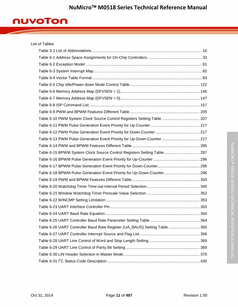
List of Tables
Table 3-1 List of Abbreviations ....................................................................................................... 16
Table 6-1 Address Space Assignments for On-Chip Controllers ................................................... 33
Table 6-2 Exception Model ............................................................................................................ 81
Table 6-3 System Interrupt Map ..................................................................................................... 82
Table 6-4 Vector Table Format ...................................................................................................... 83
Table 6-5 Chip Idle/Power-down Mode Control Table ................................................................. 122
Table 6-6 Memory Address Map (DFVSEN = 1).......................................................................... 146
Table 6-7 Memory Address Map (DFVSEN = 0).......................................................................... 147
Table 6-8 ISP Command List ....................................................................................................... 157
Table 6-9 PWM and BPWM Features Different Table ................................................................. 205
Table 6-10 PWM System Clock Source Control Registers Setting Table ................................... 207
Table 6-11 PWM Pulse Generation Event Priority for Up-Counter .............................................. 217
Table 6-12 PWM Pulse Generation Event Priority for Down-Counter ......................................... 217
Table 6-13 PWM Pulse Generation Event Priority for Up-Down-Counter ................................... 217
Table 6-14 PWM and BPWM Features Different Table ............................................................... 285
Table 6-15 BPWM System Clock Source Control Registers Setting Table ................................. 287
Table 6-16 BPWM Pulse Generation Event Priority for Up-Counter ........................................... 296
Table 6-17 BPWM Pulse Generation Event Priority for Down-Counter ....................................... 296
Table 6-18 BPWM Pulse Generation Event Priority for Up-Down-Counter ................................. 296
Table 6-19 PWM and BPWM Features Different Table ............................................................... 303
Table 6-20 Watchdog Timer Time-out Interval Period Selection ................................................. 345
Table 6-21 Window Watchdog Timer Prescale Value Selection ................................................. 352
Table 6-22 WINCMP Setting Limitation ....................................................................................... 353
Table 6-23 UART Interface Controller Pin ................................................................................... 363
Table 6-24 UART Baud Rate Equation ........................................................................................ 364
Table 6-25 UART Controller Baud Rate Parameter Setting Table .............................................. 364
Table 6-26 UART Controller Baud Rate Register (UA_BAUD) Setting Table ............................. 365
Table 6-27 UART Controller Interrupt Source and Flag List ........................................................ 368
Table 6-28 UART Line Control of Word and Stop Length Setting ............................................... 369
Table 6-29 UART Line Control of Parity Bit Setting ..................................................................... 369
Table 6-30 LIN Header Selection in Master Mode ....................................................................... 375
Table 6-31 I2C Status Code Description ...................................................................................... 430
NuMicro M0518 Series Technical Reference Manual
Oct 31, 2014 Page 12 of 497 Revision 1.00
NU
MIC
RO
™ M
0518
SE
RIE
S T
EC
HN
ICA
L R
EF
ER
EN
CE
MA
NU
AL
1 GENERAL DESCRIPTION
The NuMicro M0518 series is embedded with the Cortex™-M0 core running up to 50 MHz and features 36K/68K bytes flash, 8K bytes SRAM, and 4 Kbytes loader ROM for the ISP. It is also equipped with plenty of peripheral devices, such as Timers, Watchdog Timer (WDT), Window Watchdog Timer (WWDT), UART, SPI, I
2C, PWM, GPIO, LIN, 800 kSPS high speed 12-bit ADC,
Low Voltage Reset Controller and Brown-out Detector.
NuMicro M0518 Series Technical Reference Manual
Oct 31, 2014 Page 13 of 497 Revision 1.00
NU
MIC
RO
™ M
0518
SE
RIE
S T
EC
HN
ICA
L R
EF
ER
EN
CE
MA
NU
AL
2 FEATURES
ARM® Cortex™-M0 core – Runs up to 50 MHz – One 24-bit system timer – Supports low power sleep mode – Single-cycle 32-bit hardware multiplier – NVIC for the 32 interrupt inputs, each with 4-levels of priority – Serial Wire Debug supports with 2 watchpoints/4 breakpoints
Built-in LDO for wide operating voltage ranged from 2.5 V to 5.5 V Flash Memory
– 36K/68K bytes Flash for program code – Configurable Flash memory for data memory (Data Flash), 4 KB flash for ISP loader – Supports In-System-Program (ISP) and In-Application-Program (IAP) application code
update – 512 byte page erase for flash – Supports 2-wired ICP update through SWD/ICE interface – Supports fast parallel programming mode by external programmer
SRAM Memory – 8KB SRAM
Clock Control – Flexible selection for different applications – Built-in 22.1184 MHz high speed oscillator for system operation
Trimmed to ±1 % at +25 ℃ and VDD = 5 V
Trimmed to ±2 % at -40 ℃ ~ +105 ℃ and VDD = 2.5 V ~ 5.5 V
– Built-in 10 kHz low speed oscillator for Watchdog Timer and Wake-up operation – Supports one PLL output frequency up to 200 MHz, BPWM/PWM clock frequency up to 100
MHz, and System operation frequency up to 50 MHz – External 4~24 MHz high speed crystal input for precise timing operation
GPIO – Four I/O modes:
Quasi-bidirectional Push-pull output Open-drain output Input only with high impendence
– TTL/Schmitt trigger input selectable – I/O pin configured as interrupt source with edge/level setting
Timer – Supports 4 sets of 32-bit timers with 24-bit up-timer and one 8-bit prescale counter – Independent clock source for each timer – Provides one-shot, periodic, toggle and continuous counting operation modes – Supports event counting function – Supports input capture function
Watchdog Timer – Multiple clock sources
System clock (HCLK) Internal 10 kHz oscillator (LIRC)
– 8 selectable time-out period from 1.6 ms ~ 26.0 sec (depending on clock source) – Wake-up from Power-down or Idle mode – Interrupt or reset selectable on watchdog time-out
Window Watchdog Timer – 6-bit down counter with 11-bit prescale for wide range window selected
BPWM/Capture – Supports maximum clock frequency up to 100MHz – Supports up to two BPWM modules, each module provides one 16-bit timer and 6 output

NuMicro M0518 Series Technical Reference Manual
Oct 31, 2014 Page 14 of 497 Revision 1.00
NU
MIC
RO
™ M
0518
SE
RIE
S T
EC
HN
ICA
L R
EF
ER
EN
CE
MA
NU
AL
channels – Supports independent mode for BPWM output/Capture input channel – Supports 12-bit pre-scalar from 1 to 4096 – Supports 16-bit resolution BPWM counter
Up, down and up/down counter operation type – Supports mask function and tri-state enable for each BPWM pin – Supports interrupt on the following events:
BPWM counter match zero, period value or compared value – Supports trigger ADC on the following events:
BPWM counter match zero, period value or compared value – Supports up to 12 capture input channels with 16-bit resolution – Supports rising edges, falling edges or both edges capture condition – Supports input rising edges, falling edges or both edges capture interrupt – Supports rising edges, falling edges or both edges capture with counter reload option
PWM/Capture – Supports maximum clock frequency up to 100MHz – Supports up to two PWM modules, each module provides three 16-bit timers and 6 output
channels – Supports independent mode for PWM output/Capture input channel – Supports complementary mode for 3 complementary paired PWM output channel
Dead-time insertion with 12-bit resolution Two compared values during one period
– Supports 12-bit pre-scalar from 1 to 4096 – Supports 16-bit resolution PWM counter
Up, down and up/down counter operation type – Supports mask function and tri-state enable for each PWM pin – Supports brake function
Brake source from pin and system safety events (clock failed, Brown-out detection and CPU lockup)
Noise filter for brake source from pin Edge detect brake source to control brake state until brake interrupt cleared Level detect brake source to auto recover function after brake condition removed
– Supports interrupt on the following events: PWM counter match zero, period value or compared value Brake condition happened
– Supports trigger ADC on the following events: PWM counter match zero, period value or compared value
– Supports up to 12 capture input channels with 16-bit resolution – Supports rising edges, falling edges or both edges capture condition – Supports input rising edges, falling edges or both edges capture interrupt – Supports rising edges, falling edges or both edges capture with counter reload option
UART – Up to six UART controllers – UART0 and UART1 ports with flow control (TXD, RXD, nCTS and nRTS) – UART0, UART1 and UART2 with 16-byte FIFO for standard device – Supports IrDA (SIR) and LIN function – Supports RS-485 9-bit mode and direction control – Supports auto baud-rate generator
SPI – One set of SPI controller – Supports SPI Master/Slave mode – Full duplex synchronous serial data transfer – Variable length of transfer data from 8 to 32 bits – MSB or LSB first data transfer – Rx and Tx on both rising or falling edge of serial clock independently
NuMicro M0518 Series Technical Reference Manual
Oct 31, 2014 Page 15 of 497 Revision 1.00
NU
MIC
RO
™ M
0518
SE
RIE
S T
EC
HN
ICA
L R
EF
ER
EN
CE
MA
NU
AL
– Supports Byte Suspend mode in 32-bit transmission – Supports three wire, no slave select signal, bi-direction interface
I2C
– Up to two sets of I2C devices
– Master/Slave mode – Bidirectional data transfer between masters and slaves – Multi-master bus (no central master) – Arbitration between simultaneously transmitting masters without corruption of serial data on
the bus – Serial clock synchronization allowing devices with different bit rates to communicate via one
serial bus – Serial clock synchronization used as a handshake mechanism to suspend and resume serial
transfer – Programmable clocks allowing for versatile rate control – Supports multiple address recognition (four slave address with mask option) – Supports wake-up function
ADC – 12-bit SAR ADC with 800 kSPS – Up to 8-ch single-end input or 4-ch differential input – Single scan/single cycle scan/continuous scan – Each channel with individual result register – Scan on enabled channels – Threshold voltage detection – Conversion started by software programming or external input
96-bit unique ID (UID) 128-bit unique customer ID(UCID) Brown-out Detector
– With 4 levels: 4.4 V/3.7 V/2.7 V/2.2 V – Supports Brown-out Interrupt and Reset option
Low Voltage Reset – Threshold voltage level: 2.0 V
Operating Temperature: -40℃ ~ +105℃
Packages: – All Green package (RoHS) – LQFP 64-pin / 48-pin (7mm x 7mm)
NuMicro M0518 Series Technical Reference Manual
Oct 31, 2014 Page 16 of 497 Revision 1.00
NU
MIC
RO
™ M
0518
SE
RIE
S T
EC
HN
ICA
L R
EF
ER
EN
CE
MA
NU
AL
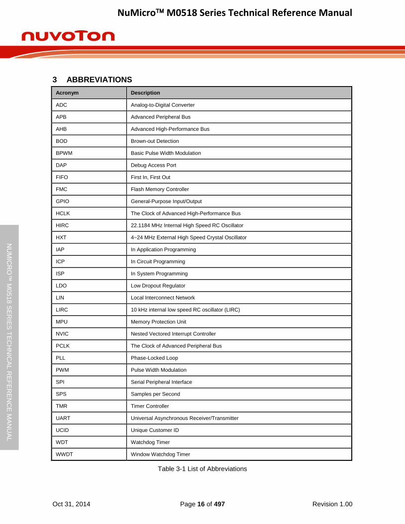
3 ABBREVIATIONS
Acronym Description
ADC Analog-to-Digital Converter
APB Advanced Peripheral Bus
AHB Advanced High-Performance Bus
BOD Brown-out Detection
BPWM Basic Pulse Width Modulation
DAP Debug Access Port
FIFO First In, First Out
FMC Flash Memory Controller
GPIO General-Purpose Input/Output
HCLK The Clock of Advanced High-Performance Bus
HIRC 22.1184 MHz Internal High Speed RC Oscillator
HXT 4~24 MHz External High Speed Crystal Oscillator
IAP In Application Programming
ICP In Circuit Programming
ISP In System Programming
LDO Low Dropout Regulator
LIN Local Interconnect Network
LIRC 10 kHz internal low speed RC oscillator (LIRC)
MPU Memory Protection Unit
NVIC Nested Vectored Interrupt Controller
PCLK The Clock of Advanced Peripheral Bus
PLL Phase-Locked Loop
PWM Pulse Width Modulation
SPI Serial Peripheral Interface
SPS Samples per Second
TMR Timer Controller
UART Universal Asynchronous Receiver/Transmitter
UCID Unique Customer ID
WDT Watchdog Timer
WWDT Window Watchdog Timer
Table 3-1 List of Abbreviations
NuMicro M0518 Series Technical Reference Manual
Oct 31, 2014 Page 17 of 497 Revision 1.00
NU
MIC
RO
™ M
0518
SE
RIE
S T
EC
HN
ICA
L R
EF
ER
EN
CE
MA
NU
AL
4 PARTS INFORMATION LIST AND PIN CONFIGURATION
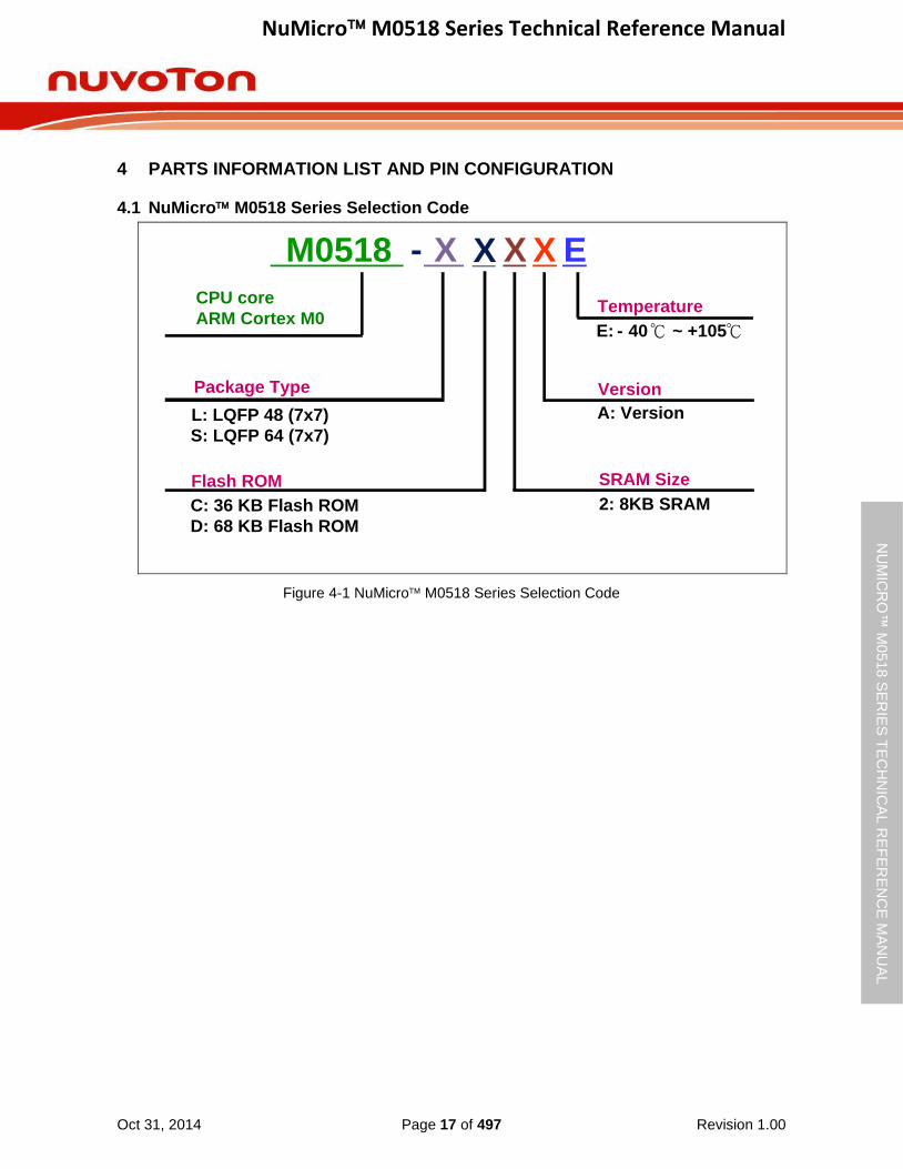
4.1 NuMicro M0518 Series Selection Code
CPU core
ARM Cortex M0
Package Type
L: LQFP 48 (7x7)
Flash ROM
C: 36 KB Flash ROM
D: 68 KB Flash ROM
Temperature
E: - 40℃ ~ +105℃
Version
A: Version
M0518 - X X E
S: LQFP 64 (7x7)
X X
SRAM Size
2: 8KB SRAM
Figure 4-1 NuMicro M0518 Series Selection Code

NuMicro M0518 Series Technical Reference Manual
Oct 31, 2014 Page 18 of 497 Revision 1.00
NU
MIC
RO
™ M
0518
SE
RIE
S T
EC
HN
ICA
L R
EF
ER
EN
CE
MA
NU
AL
4.2 NuMicro M0518 Series Selection Guide P
art
Nu
mb
er
AP
RO
M (
KB
)
RA
M (
KB
)
Data
Fla
sh
(K
B)
ISP
R
OM
(K
B)
I/O
Tim
er
(32-B
it)
Connectivity
PW
M (
16-B
it)
AD
C (
12-B
it)
ISP
/IC
P/IA
P
Packag
e
UA
RT
SP
I
I2C
LIN
M0518LC2AE 36 8 Configurable 4 42 4 6 1 2 3 24 8 ch √ LQFP48
M0518LD2AE 68 8 Configurable 4 42 4 6 1 2 3 24 8 ch √ LQFP48
M0518SC2AE 36 8 Configurable 4 56 4 6 1 2 3 24 8 ch √ LQFP64
M0518SD2AE 68 8 Configurable 4 56 4 6 1 2 3 24 8 ch √ LQFP64
NuMicro M0518 Series Technical Reference Manual
Oct 31, 2014 Page 19 of 497 Revision 1.00
NU
MIC
RO
™ M
0518
SE
RIE
S T
EC
HN
ICA
L R
EF
ER
EN
CE
MA
NU
AL
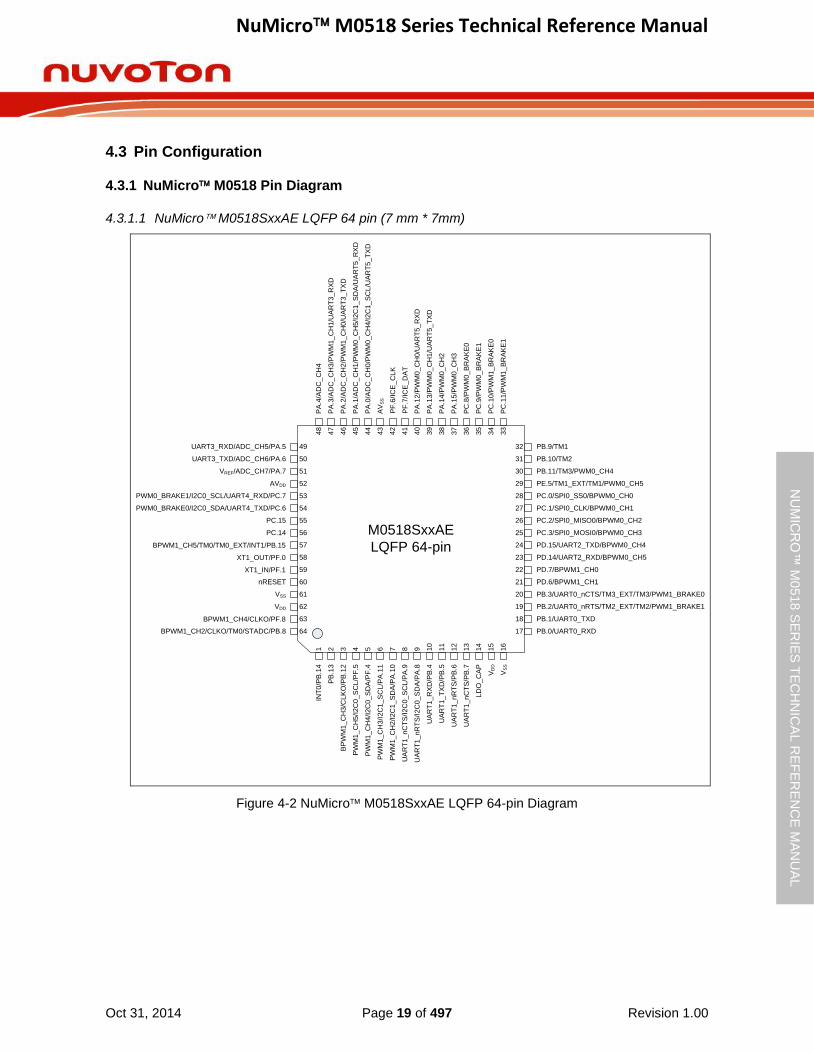
4.3 Pin Configuration
4.3.1 NuMicro M0518 Pin Diagram
4.3.1.1 NuMicro M0518SxxAE LQFP 64 pin (7 mm * 7mm)
UART3_RXD/ADC_CH5/PA.5
UART3_TXD/ADC_CH6/PA.6
INT
0/P
B.1
4
PB
.13
BP
WM
1_
CH
3/C
LK
O/P
B.1
2
PW
M1
_C
H4
/I2
C0
_S
DA
/PF
.4
PW
M1
_C
H5
/I2
C0
_S
CL
/PF
.5
PW
M1
_C
H3
/I2
C1
_S
CL
/PA
.11
PW
M1
_C
H2
/I2
C1
_S
DA
/PA
.10
UA
RT
1_
nC
TS
/I2
C0
_S
CL
/PA
.9
UA
RT
1_
nR
TS
/I2
C0
_S
DA
/PA
.8
UA
RT
1_
RX
D/P
B.4
UA
RT
1_
TX
D/P
B.5
UA
RT
1_
nR
TS
/PB
.6
UA
RT
1_
nC
TS
/PB
.7
LD
O_
CA
P
VD
D
VS
S
PWM0_BRAKE1/I2C0_SCL/UART4_RXD/PC.7
PWM0_BRAKE0/I2C0_SDA/UART4_TXD/PC.6
PC.15
PC.14
nRESET
BPWM1_CH2/CLKO/TM0/STADC/PB.8
PA
.4/A
DC
_C
H4
PA
.3/A
DC
_C
H3
/PW
M1
_C
H1
/UA
RT
3_
RX
D
PA
.2/A
DC
_C
H2
/PW
M1
_C
H0
/UA
RT
3_
TX
D
PA
.1/A
DC
_C
H1
/PW
M0
_C
H5
/I2
C1
_S
DA
/UA
RT
5_
RX
D
PA
.0/A
DC
_C
H0
/PW
M0
_C
H4
/I2
C1
_S
CL/U
AR
T5
_T
XD
AV
SS
PA
.12
/PW
M0
_C
H0
/UA
RT
5_
RX
D
PA
.13
/PW
M0
_C
H1
/UA
RT
5_
TX
D
PA
.14
/PW
M0
_C
H2
PA
.15
/PW
M0
_C
H3
PC
.8/P
WM
0_
BR
AK
E0
PC
.9/P
WM
0_
BR
AK
E1
AVDD
VSS
VDD
PC.0/SPI0_SS0/BPWM0_CH0
PC.1/SPI0_CLK/BPWM0_CH1
PC.2/SPI0_MISO0/BPWM0_CH2
PC.3/SPI0_MOSI0/BPWM0_CH3
PD.15/UART2_TXD/BPWM0_CH4
PD.14/UART2_RXD/BPWM0_CH5
PD.7/BPWM1_CH0
PD.6/BPWM1_CH1
PB.3/UART0_nCTS/TM3_EXT/TM3/PWM1_BRAKE0
PB.2/UART0_nRTS/TM2_EXT/TM2/PWM1_BRAKE1
PB.1/UART0_TXD
PB.0/UART0_RXD17
18
19
20
21
22
23
24
25
26
27
28
29
30
31
32
64
63
62
61
60
59
58
57
56
55
54
53
52
51
50
49
16
15
14
13
12
11
10
987654321
33
34
35
36
37
38
39
40
41
42
43
44
45
46
47
48
PC
.10
/PW
M1
_B
RA
KE
0
PC
.11
/PW
M1
_B
RA
KE
1
PB.9/TM1
PB.10/TM2
PB.11/TM3/PWM0_CH4
PE.5/TM1_EXT/TM1/PWM0_CH5
VREF/ADC_CH7/PA.7
PF
.6/IC
E_
CL
K
PF
.7/IC
E_
DA
T
M0518SxxAE
LQFP 64-pin
BPWM1_CH4/CLKO/PF.8
XT1_OUT/PF.0
BPWM1_CH5/TM0/TM0_EXT/INT1/PB.15
XT1_IN/PF.1
Figure 4-2 NuMicro M0518SxxAE LQFP 64-pin Diagram
NuMicro M0518 Series Technical Reference Manual
Oct 31, 2014 Page 20 of 497 Revision 1.00
NU
MIC
RO
™ M
0518
SE
RIE
S T
EC
HN
ICA
L R
EF
ER
EN
CE
MA
NU
AL
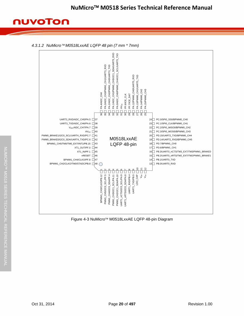
4.3.1.2 NuMicro M0518LxxAE LQFP 48 pin (7 mm * 7mm)
UART3_RXD/ADC_CH5/PA.5
UART3_TXD/ADC_CH6/PA.6
VREF/ADC_CH7/PA.7
BP
WM
1_
CH
3/C
LK
O/P
B.1
2
PW
M1
_C
H4
/I2
C0
_S
DA
/PF
.4
PW
M1
_C
H5
/I2
C0
_S
CL
/PF
.5
PW
M1
_C
H3
/I2
C1
_S
CL
/PA
.11
PW
M1_
CH
2/I
2C
1_
SD
A/P
A.1
0
UA
RT
1_
nC
TS
/I2
C0
_S
CL
/PA
.9
UA
RT
1_
nR
TS
/I2
C0
_S
DA
/PA
.8
UA
RT
1_
RX
D/P
B.4
UA
RT
1_
TX
D/P
B.5
LD
O_
CA
P
VD
D
VS
S
PWM0_BRAKE1/I2C0_SCL/UART4_RXD/PC.7
PWM0_BRAKE0/I2C0_SDA/UART4_TXD/PC.6
nRESET
BPWM1_CH2/CLKO/TM0/STADC/PB.8
PA
.4/A
DC
_C
H4
PA
.3/A
DC
_C
H3
/PW
M1
_C
H1
/UA
RT
3_
RX
D
PA
.2/A
DC
_C
H2
/PW
M1
_C
H0
/UA
RT
3_
TX
D
PA
.1/A
DC
_C
H1
/PW
M0
_C
H5
/I2
C1
_S
DA
/UA
RT
5_
RX
D
PA
.0/A
DC
_C
H0
/PW
M0
_C
H4
/I2
C1
_S
CL/U
AR
T5
_T
XD
AV
SS
PA
.12/P
WM
0_
CH
0/U
AR
T5
_R
XD
PA
.13/P
WM
0_
CH
1/U
AR
T5
_T
XD
PA
.14/P
WM
0_
CH
2
PA
.15/P
WM
0_
CH
3
AVDD
PC.0/SPI0_SS0/BPWM0_CH0
PC.1/SPI0_CLK/BPWM0_CH1
PC.2/SPI0_MISO0/BPWM0_CH2
PC.3/SPI0_MOSI0/BPWM0_CH3
PD.7/BPWM1_CH0
PD.6/BPWM1_CH1
PB.3/UART0_nCTS/TM3_EXT/TM3/PWM1_BRAKE0
PB.2/UART0_nRTS/TM2_EXT/TM2/PWM1_BRAKE1
13
14
15
16
17
18
19
20
21
22
23
24
48
47
46
45
44
43
42
41
40
39
38
37
12
11
10
987654321
25
26
27
28
29
30
31
32
33
34
35
36
M0518LxxAE
LQFP 48-pin
PD.15/UART2_TXD/BPWM0_CH4
PD.14/UART2_RXD/BPWM0_CH5
PB.1/UART0_TXD
PB.0/UART0_RXD
PF
.6/IC
E_
CL
K
PF
.7/IC
E_
DA
T
BPWM1_CH4/CLKO/PF.8
XT1_OUT/PF.0
BPWM1_CH5/TM0/TM0_EXT/INT1/PB.15
XT1_IN/PF.1
Figure 4-3 NuMicro M0518LxxAE LQFP 48-pin Diagram

NuMicro M0518 Series Technical Reference Manual
Oct 31, 2014 Page 21 of 497 Revision 1.00
NU
MIC
RO
™ M
0518
SE
RIE
S T
EC
HN
ICA
L R
EF
ER
EN
CE
MA
NU
AL
4.4 Pin Description
4.4.1 NuMicro M0518 Pin Description
Pin No.
Pin Name Pin
Type Description
LQFP 64-pin
LQFP 48-pin
1 PB.14 I/O General purpose digital I/O pin.
INT0 I External interrupt0 input pin.
2 PB.13 I/O General purpose digital I/O pin.
3 1
PB.12 I/O General purpose digital I/O pin.
CLKO O Frequency divider clock output pin.
BPWM1_CH3 I/O BPWM1 CH3 output/Capture input.
4 2
PF.5 I/O General purpose digital I/O pin.
I2C0_SCL I/O I2C0 clock pin.
PWM1_CH5 I/O PWM1 CH5 output/Capture input.
5 3
PF.4 I/O General purpose digital I/O pin.
I2C0_SDA I/O I2C0 data input/output pin.
PWM1_CH4 I/O PWM1 CH4 output/Capture input.
6 4
PA.11 I/O General purpose digital I/O pin.
I2C1_SCL I/O I2C1 clock pin.
PWM1_CH3 I/O PWM1 CH3 output/Capture input.
7 5
PA.10 I/O General purpose digital I/O pin.
I2C1_SDA I/O I2C1 data input/output pin.
PWM1_CH2 I/O PWM1 CH2 output/Capture input.
8 6
PA.9 I/O General purpose digital I/O pin.
I2C0_SCL I/O I2C0 clock pin.
UART1_nCTS I Clear to Send input pin for UART1.
9 7
PA.8 I/O General purpose digital I/O pin.
I2C0_SDA I/O I2C0 data input/output pin.
UART1_nRTS O Request to Send output pin for UART1.
10 8 PB.4 I/O General purpose digital I/O pin.
UART1_RXD I Data receiver input pin for UART1.
11 9 PB.5 I/O General purpose digital I/O pin.
UART1_TXD O Data transmitter output pin for UART1.
12 PB.6 I/O General purpose digital I/O pin.

NuMicro M0518 Series Technical Reference Manual
Oct 31, 2014 Page 22 of 497 Revision 1.00
NU
MIC
RO
™ M
0518
SE
RIE
S T
EC
HN
ICA
L R
EF
ER
EN
CE
MA
NU
AL
Pin No.
Pin Name Pin
Type Description
LQFP 64-pin
LQFP 48-pin
UART1_nRTS O Request to Send output pin for UART1.
13 PB.7 I/O General purpose digital I/O pin.
UART1_nCTS I Clear to Send input pin for UART1.
14 10 LDO_CAP P LDO output pin.
15 11 VDD P Power supply for I/O ports and LDO source for internal PLL and digital circuit.
16 12 VSS P Ground pin for digital circuit.
17 13 PB.0 I/O General purpose digital I/O pin.
UART0_RXD I Data receiver input pin for UART0.
18 14 PB.1 I/O General purpose digital I/O pin.
UART0_TXD O Data transmitter output pin for UART0.
19 15
PB.2 I/O General purpose digital I/O pin.
UART0_nRTS O Request to Send output pin for UART0.
TM2_EXT I Timer2 external capture input pin.
TM2 O Timer2 toggle output pin.
PWM1_BRAKE1 I PWM1 brake input pin.
20 16
PB.3 I/O General purpose digital I/O pin.
UART0_nCTS I Clear to Send input pin for UART0.
TM3_EXT I Timer3 external capture input pin.
TM3 O Timer3 toggle output pin.
PWM1_BRAKE0 I PWM1 brake input pin.
21 17 PD.6 I/O General purpose digital I/O pin.
BPWM1_CH1 I/O BPWM1 CH1 output/Capture input.
22 18 PD.7 I/O General purpose digital I/O pin.
BPWM1_CH0 I/O BPWM1 CH0 output/Capture input.
23 19
PD.14 I/O General purpose digital I/O pin.
UART2_RXD I Data receiver input pin for UART2.
BPWM0_CH5 I/O BPWM0 CH5 output/Capture input.
24 20
PD.15 I/O General purpose digital I/O pin.
UART2_TXD O Data transmitter output pin for UART2.
BPWM0_CH4 I/O BPWM0 CH4 input/Capture input.
25 21 PC.3 I/O General purpose digital I/O pin.
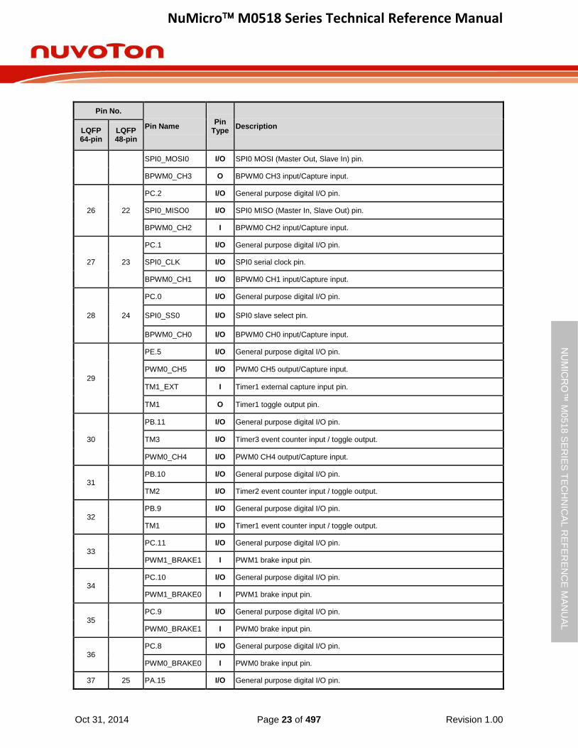
NuMicro M0518 Series Technical Reference Manual
Oct 31, 2014 Page 23 of 497 Revision 1.00
NU
MIC
RO
™ M
0518
SE
RIE
S T
EC
HN
ICA
L R
EF
ER
EN
CE
MA
NU
AL
Pin No.
Pin Name Pin
Type Description
LQFP 64-pin
LQFP 48-pin
SPI0_MOSI0 I/O SPI0 MOSI (Master Out, Slave In) pin.
BPWM0_CH3 O BPWM0 CH3 input/Capture input.
26 22
PC.2 I/O General purpose digital I/O pin.
SPI0_MISO0 I/O SPI0 MISO (Master In, Slave Out) pin.
BPWM0_CH2 I BPWM0 CH2 input/Capture input.
27 23
PC.1 I/O General purpose digital I/O pin.
SPI0_CLK I/O SPI0 serial clock pin.
BPWM0_CH1 I/O BPWM0 CH1 input/Capture input.
28 24
PC.0 I/O General purpose digital I/O pin.
SPI0_SS0 I/O SPI0 slave select pin.
BPWM0_CH0 I/O BPWM0 CH0 input/Capture input.
29
PE.5 I/O General purpose digital I/O pin.
PWM0_CH5 I/O PWM0 CH5 output/Capture input.
TM1_EXT I Timer1 external capture input pin.
TM1 O Timer1 toggle output pin.
30
PB.11 I/O General purpose digital I/O pin.
TM3 I/O Timer3 event counter input / toggle output.
PWM0_CH4 I/O PWM0 CH4 output/Capture input.
31 PB.10 I/O General purpose digital I/O pin.
TM2 I/O Timer2 event counter input / toggle output.
32 PB.9 I/O General purpose digital I/O pin.
TM1 I/O Timer1 event counter input / toggle output.
33 PC.11 I/O General purpose digital I/O pin.
PWM1_BRAKE1 I PWM1 brake input pin.
34 PC.10 I/O General purpose digital I/O pin.
PWM1_BRAKE0 I PWM1 brake input pin.
35 PC.9 I/O General purpose digital I/O pin.
PWM0_BRAKE1 I PWM0 brake input pin.
36 PC.8 I/O General purpose digital I/O pin.
PWM0_BRAKE0 I PWM0 brake input pin.
37 25 PA.15 I/O General purpose digital I/O pin.
NuMicro M0518 Series Technical Reference Manual
Oct 31, 2014 Page 24 of 497 Revision 1.00
NU
MIC
RO
™ M
0518
SE
RIE
S T
EC
HN
ICA
L R
EF
ER
EN
CE
MA
NU
AL
Pin No.
Pin Name Pin
Type Description
LQFP 64-pin
LQFP 48-pin
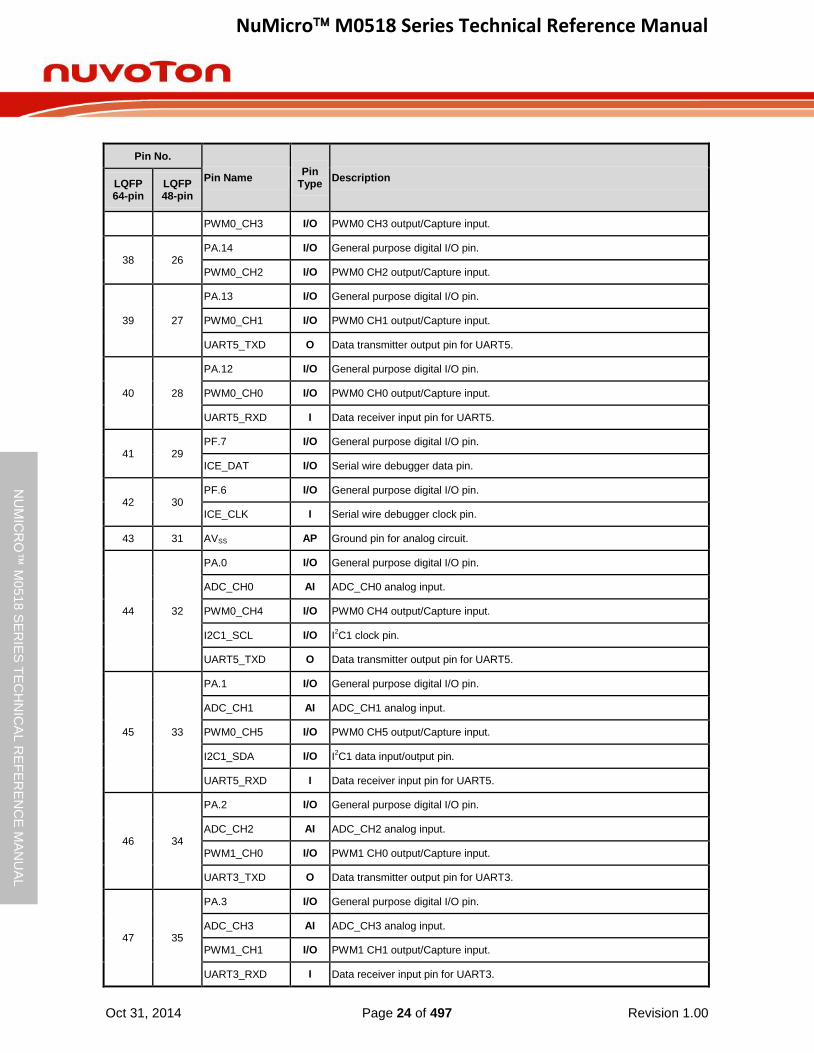
PWM0_CH3 I/O PWM0 CH3 output/Capture input.
38 26 PA.14 I/O General purpose digital I/O pin.
PWM0_CH2 I/O PWM0 CH2 output/Capture input.
39 27
PA.13 I/O General purpose digital I/O pin.
PWM0_CH1 I/O PWM0 CH1 output/Capture input.
UART5_TXD O Data transmitter output pin for UART5.
40 28
PA.12 I/O General purpose digital I/O pin.
PWM0_CH0 I/O PWM0 CH0 output/Capture input.
UART5_RXD I Data receiver input pin for UART5.
41 29 PF.7 I/O General purpose digital I/O pin.
ICE_DAT I/O Serial wire debugger data pin.
42 30 PF.6 I/O General purpose digital I/O pin.
ICE_CLK I Serial wire debugger clock pin.
43 31 AVSS AP Ground pin for analog circuit.
44 32
PA.0 I/O General purpose digital I/O pin.
ADC_CH0 AI ADC_CH0 analog input.
PWM0_CH4 I/O PWM0 CH4 output/Capture input.
I2C1_SCL I/O I2C1 clock pin.
UART5_TXD O Data transmitter output pin for UART5.
45 33
PA.1 I/O General purpose digital I/O pin.
ADC_CH1 AI ADC_CH1 analog input.
PWM0_CH5 I/O PWM0 CH5 output/Capture input.
I2C1_SDA I/O I2C1 data input/output pin.
UART5_RXD I Data receiver input pin for UART5.
46 34
PA.2 I/O General purpose digital I/O pin.
ADC_CH2 AI ADC_CH2 analog input.
PWM1_CH0 I/O PWM1 CH0 output/Capture input.
UART3_TXD O Data transmitter output pin for UART3.
47 35
PA.3 I/O General purpose digital I/O pin.
ADC_CH3 AI ADC_CH3 analog input.
PWM1_CH1 I/O PWM1 CH1 output/Capture input.
UART3_RXD I Data receiver input pin for UART3.

NuMicro M0518 Series Technical Reference Manual
Oct 31, 2014 Page 25 of 497 Revision 1.00
NU
MIC
RO
™ M
0518
SE
RIE
S T
EC
HN
ICA
L R
EF
ER
EN
CE
MA
NU
AL
Pin No.
Pin Name Pin
Type Description
LQFP 64-pin
LQFP 48-pin
48 36 PA.4 I/O General purpose digital I/O pin.
ADC_CH4 AI ADC_CH4 analog input.
49 37
PA.5 I/O General purpose digital I/O pin.
ADC_CH5 AI ADC_CH5 analog input.
UART3_RXD I Data receiver input pin for UART3.
50 38
PA.6 I/O General purpose digital I/O pin.
ADC_CH6 AI ADC_CH6 analog input.
UART3_TXD O Data transmitter output pin for UART3.
51 39
PA.7 I/O General purpose digital I/O pin.
ADC_CH7 AI ADC_CH7 analog input.
VREF AP Voltage reference input for ADC.
52 40 AVDD AP Power supply for internal analog circuit.
53 41
PC.7 I/O General purpose digital I/O pin.
UART4_RXD I Data reveiver input pin for UART4.
I2C0_SCL I/O I2C0 clock pin.
PWM0_BRAKE1 I PWM0 brake input pin.
54 42
PC.6 I/O General purpose digital I/O pin.
UART4_TXD O Data transmitter output pin for UART4.
I2C0_SDA I/O I2C0 data input/output pin.
PWM0_BRAKE0 I PWM0 brake input pin.
55 PC.15 I/O General purpose digital I/O pin.
56 PC.14 I/O General purpose digital I/O pin.
57 43
PB.15 I/O General purpose digital I/O pin.
INT1 I External interrupt1 input pin.
TM0_EXT I Timer0 external capture input pin.
TM0 O Timer0 toggle output pin.
BPWM1_CH5 I/O BPWM1 CH5 output/Capture input.
58 44 PF.0 I/O General purpose digital I/O pin.
XT1_OUT O External 4~24 MHz (high speed) crystal output pin.
59 45 PF.1 I/O General purpose digital I/O pin.
XT1_IN I External 4~24 MHz (high speed) crystal input pin.
60 46 nRESET I External reset input: active LOW, with an internal pull-up. Set this pin low reset
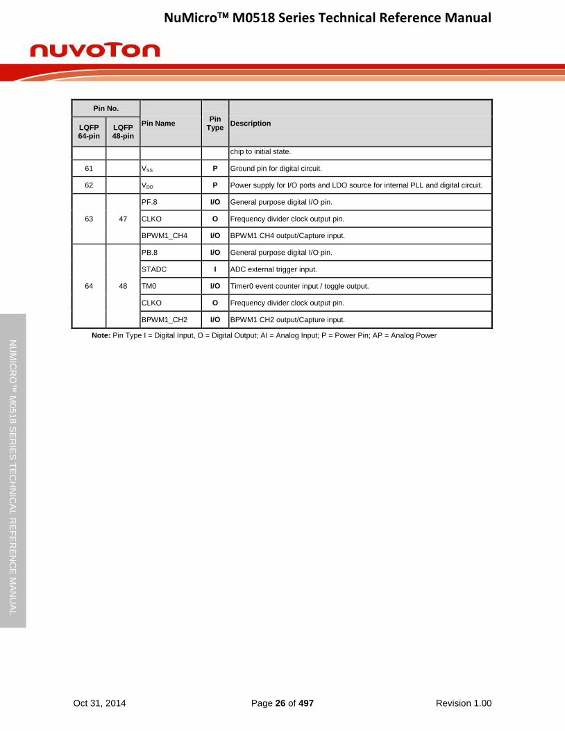
NuMicro M0518 Series Technical Reference Manual
Oct 31, 2014 Page 26 of 497 Revision 1.00
NU
MIC
RO
™ M
0518
SE
RIE
S T
EC
HN
ICA
L R
EF
ER
EN
CE
MA
NU
AL
Pin No.
Pin Name Pin
Type Description
LQFP 64-pin
LQFP 48-pin
chip to initial state.
61 VSS P Ground pin for digital circuit.
62 VDD P Power supply for I/O ports and LDO source for internal PLL and digital circuit.
63 47
PF.8 I/O General purpose digital I/O pin.
CLKO O Frequency divider clock output pin.
BPWM1_CH4 I/O BPWM1 CH4 output/Capture input.
64 48
PB.8 I/O General purpose digital I/O pin.
STADC I ADC external trigger input.
TM0 I/O Timer0 event counter input / toggle output.
CLKO O Frequency divider clock output pin.
BPWM1_CH2 I/O BPWM1 CH2 output/Capture input.
Note: Pin Type I = Digital Input, O = Digital Output; AI = Analog Input; P = Power Pin; AP = Analog Power

NuMicro M0518 Series Technical Reference Manual
Oct 31, 2014 Page 27 of 497 Revision 1.00
NU
MIC
RO
™ M
0518
SE
RIE
S T
EC
HN
ICA
L R
EF
ER
EN
CE
MA
NU
AL
5 BLOCK DIAGRAM
5.1 NuMicro M0518 Block Diagram
Bridge
32-bit Timer X 4
Watchdog Timers X 2
16-bit PWM 24
Channels
Timer / PWM Analog Interface
12-bit ADC X 8-ch
with VREF
APROM 36/68 KB
LDROM 4 KB
Configurable
Data Flash
SRAM 8KB
Memory
ARM
CortexTM –M0
50 MHz
Clock Control
High Speed Oscillator
22.1184 MHz
Low Speed Oscillator 10 kHz
High Speed External
Crystal Oscillator 4~24 MHz
PLL
GPIO
General Purpose I/O
External Interrupt
Power Control Connectivity
UART X 6
SPI X 1
I²C X 2
AHB Bus APB Bus
LDO 1.8V
Power On Reset
LVR
Brownout Detection
VREF
Figure 5-1 NuMicro M0518 Block Diagram

NuMicro M0518 Series Technical Reference Manual
Oct 31, 2014 Page 28 of 497 Revision 1.00
NU
MIC
RO
™ M
0518
SE
RIE
S T
EC
HN
ICA
L R
EF
ER
EN
CE
MA
NU
AL
6 FUNCTIONAL DESCRIPTION
6.1 ARM® Cortex™-M0 Core
The Cortex™-M0 processor is a configurable, multistage, 32-bit RISC processor, which has an AMBA AHB-Lite interface and includes an NVIC component. It also has optional hardware debug functionality. The processor can execute Thumb code and is compatible with other Cortex™-M profile processor. The profile supports two modes -Thread mode and Handler mode. Handler mode is entered as a result of an exception. An exception return can only be issued in Handler mode. Thread mode is entered on Reset, and can be entered as a result of an exception return.
Figure 6-1 shows the functional controller of processor.
CortexTM
-M0
Processor
Core
Nested
Vectored
Interrupt
Controller
(NVIC)
Breakpoint
and
Watchpoint
Unit
Debugger
InterfaceBus Matrix
Debug
Access
Port
(DAP)
DebugCortexTM
-M0 processor
CortexTM
-M0 Components
Wakeup
Interrupt
Controller
(WIC)
Interrupts
Serial Wire or
JTAG Debug Port
AHB-Lite
Interface
Figure 6-1 Functional Controller Diagram
The implemented device provides the following components and features:
A low gate count processor:
- ARMv6-M Thumb® instruction set
- Thumb-2 technology
- ARMv6-M compliant 24-bit SysTick timer
- A 32-bit hardware multiplier
- System interface supported with little-endian data accesses
- Ability to have deterministic, fixed-latency, interrupt handling
- Load/store-multiples and multicycle-multiplies that can be abandoned and restarted to facilitate rapid interrupt handling
- C Application Binary Interface compliant exception model. This is the ARMv6-M, C Application Binary Interface (C-ABI) compliant exception model that enables the use of pure C functions as interrupt handlers
- Low Power Sleep mode entry using Wait For Interrupt (WFI), Wait For Event
NuMicro M0518 Series Technical Reference Manual
Oct 31, 2014 Page 29 of 497 Revision 1.00
NU
MIC
RO
™ M
0518
SE
RIE
S T
EC
HN
ICA
L R
EF
ER
EN
CE
MA
NU
AL
(WFE) instructions, or the return from interrupt sleep-on-exit feature
NVIC:
- 32 external interrupt inputs, each with four levels of priority
- Dedicated Non-maskable Interrupt (NMI) input
- Supports for both level-sensitive and pulse-sensitive interrupt lines
- Supports Wake-up Interrupt Controller (WIC) and, providing Ultra-low Power Sleep mode
Debug support
- Four hardware breakpoints
- Two watchpoints
- Program Counter Sampling Register (PCSR) for non-intrusive code profiling
- Single step and vector catch capabilities
Bus interfaces:
- Single 32-bit AMBA-3 AHB-Lite system interface that provides simple integration to all system peripherals and memory
- Single 32-bit slave port that supports the DAP (Debug Access Port)
NuMicro M0518 Series Technical Reference Manual
Oct 31, 2014 Page 30 of 497 Revision 1.00
NU
MIC
RO
™ M
0518
SE
RIE
S T
EC
HN
ICA
L R
EF
ER
EN
CE
MA
NU
AL
6.2 System Manager
6.2.1 Overview
System management includes the following sections:
System Resets
System Memory Map
System management registers for Part Number ID, chip reset and on-chip controllers reset , multi-functional pin control
System Timer (SysTick)
Nested Vectored Interrupt Controller (NVIC)
System Control registers
6.2.2 System Reset
The system reset can be issued by one of the following listed events. For these reset event flags can be read by RSTSRC register.
Power-on Reset
Low level on the nRESET pin
Watchdog Time-out Reset
Low Voltage Reset
Brown-out Detector Reset
CPU Reset
System Reset
System Reset and Power-on Reset all reset the whole chip including all peripherals. The difference between System Reset and Power-on Reset is external crystal circuit and BS (ISPCON[1]) bit. System Reset does not reset external crystal circuit and BS (ISPCON[1]) bit, but Power-on Reset does.
NuMicro M0518 Series Technical Reference Manual
Oct 31, 2014 Page 31 of 497 Revision 1.00
NU
MIC
RO
™ M
0518
SE
RIE
S T
EC
HN
ICA
L R
EF
ER
EN
CE
MA
NU
AL
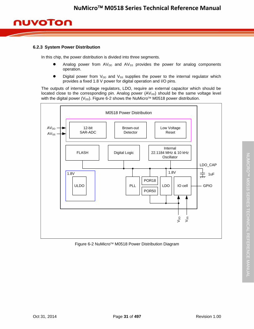
6.2.3 System Power Distribution
In this chip, the power distribution is divided into three segments.
Analog power from AVDD and AVSS provides the power for analog components operation.
Digital power from VDD and VSS supplies the power to the internal regulator which provides a fixed 1.8 V power for digital operation and I/O pins.
The outputs of internal voltage regulators, LDO, require an external capacitor which should be located close to the corresponding pin. Analog power (AVDD) should be the same voltage level
with the digital power (VDD). Figure 6-2 shows the NuMicro M0518 power distribution.
12-bit
SAR-ADC
Brown-out
Detector
Low Voltage
Reset
FLASH Digital Logic
Internal
22.1184 MHz & 10 kHz
Oscillator
AVDD
AVSS
LDO_CAP
1uF
GPIO
M0518 Power Distribution
LDOPLL
POR50
POR18 V
DD
VS
SIO cellULDO
1.8V 1.8V
Figure 6-2 NuMicro M0518 Power Distribution Diagram
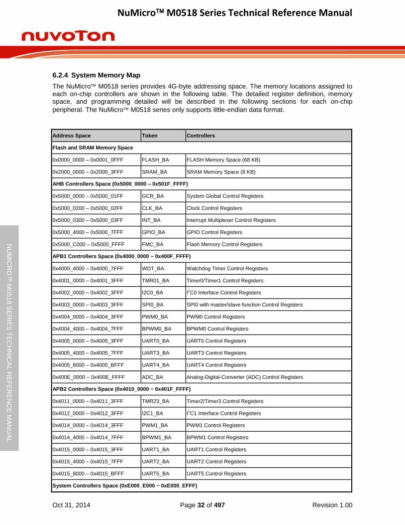
NuMicro M0518 Series Technical Reference Manual
Oct 31, 2014 Page 32 of 497 Revision 1.00
NU
MIC
RO
™ M
0518
SE
RIE
S T
EC
HN
ICA
L R
EF
ER
EN
CE
MA
NU
AL
6.2.4 System Memory Map
The NuMicro M0518 series provides 4G-byte addressing space. The memory locations assigned to each on-chip controllers are shown in the following table. The detailed register definition, memory space, and programming detailed will be described in the following sections for each on-chip
peripheral. The NuMicro M0518 series only supports little-endian data format.
Address Space Token Controllers
Flash and SRAM Memory Space
0x0000_0000 – 0x0001_0FFF FLASH_BA FLASH Memory Space (68 KB)
0x2000_0000 – 0x2000_3FFF SRAM_BA SRAM Memory Space (8 KB)
AHB Controllers Space (0x5000_0000 – 0x501F_FFFF)
0x5000_0000 – 0x5000_01FF GCR_BA System Global Control Registers
0x5000_0200 – 0x5000_02FF CLK_BA Clock Control Registers
0x5000_0300 – 0x5000_03FF INT_BA Interrupt Multiplexer Control Registers
0x5000_4000 – 0x5000_7FFF GPIO_BA GPIO Control Registers
0x5000_C000 – 0x5000_FFFF FMC_BA Flash Memory Control Registers
APB1 Controllers Space (0x4000_0000 ~ 0x400F_FFFF)
0x4000_4000 – 0x4000_7FFF WDT_BA Watchdog Timer Control Registers
0x4001_0000 – 0x4001_3FFF TMR01_BA Timer0/Timer1 Control Registers
0x4002_0000 – 0x4002_3FFF I2C0_BA I2C0 Interface Control Registers
0x4003_0000 – 0x4003_3FFF SPI0_BA SPI0 with master/slave function Control Registers
0x4004_0000 – 0x4004_3FFF PWM0_BA PWM0 Control Registers
0x4004_4000 – 0x4004_7FFF BPWM0_BA BPWM0 Control Registers
0x4005_0000 – 0x4005_3FFF UART0_BA UART0 Control Registers
0x4005_4000 – 0x4005_7FFF UART3_BA UART3 Control Registers
0x4005_8000 – 0x4005_BFFF UART4_BA UART4 Control Registers
0x400E_0000 – 0x400E_FFFF ADC_BA Analog-Digital-Converter (ADC) Control Registers
APB2 Controllers Space (0x4010_0000 ~ 0x401F_FFFF)
0x4011_0000 – 0x4011_3FFF TMR23_BA Timer2/Timer3 Control Registers
0x4012_0000 – 0x4012_3FFF I2C1_BA I2C1 Interface Control Registers
0x4014_0000 – 0x4014_3FFF PWM1_BA PWM1 Control Registers
0x4014_4000 – 0x4014_7FFF BPWM1_BA BPWM1 Control Registers
0x4015_0000 – 0x4015_3FFF UART1_BA UART1 Control Registers
0x4015_4000 – 0x4015_7FFF UART2_BA UART2 Control Registers
0x4015_8000 – 0x4015_BFFF UART5_BA UART5 Control Registers
System Controllers Space (0xE000_E000 ~ 0xE000_EFFF)
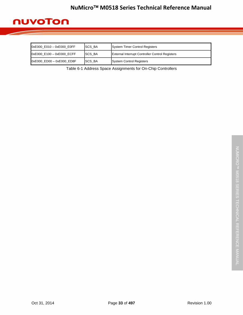
NuMicro M0518 Series Technical Reference Manual
Oct 31, 2014 Page 33 of 497 Revision 1.00
NU
MIC
RO
™ M
0518
SE
RIE
S T
EC
HN
ICA
L R
EF
ER
EN
CE
MA
NU
AL
0xE000_E010 – 0xE000_E0FF SCS_BA System Timer Control Registers
0xE000_E100 – 0xE000_ECFF SCS_BA External Interrupt Controller Control Registers
0xE000_ED00 – 0xE000_ED8F SCS_BA System Control Registers
Table 6-1 Address Space Assignments for On-Chip Controllers

NuMicro M0518 Series Technical Reference Manual
Oct 31, 2014 Page 34 of 497 Revision 1.00
NU
MIC
RO
™ M
0518
SE
RIE
S T
EC
HN
ICA
L R
EF
ER
EN
CE
MA
NU
AL
6.2.5 Register Map
R: read only, W: write only, R/W: both read and write
Register Offset R/W Description Reset Value
GCR Base Address:
GCR_BA = 0x5000_0000
PDID GCR_BA+0x00 R Part Device Identification Number Register 0x2014_0018[1]
RSTSRC GCR_BA+0x04 R/W System Reset Source Register 0x0000_00XX
IPRSTC1 GCR_BA+0x08 R/W Peripheral Reset Control Register 1 0x0000_0000
IPRSTC2 GCR_BA+0x0C R/W Peripheral Reset Control Register 2 0x0000_0000
IPRSTC3 GCR_BA+0x10 R/W Peripheral Reset Control Register 3 0x0000_0000
BODCR GCR_BA+0x18 R/W Brown-out Detector Control Register 0x0000_038X
PORCR GCR_BA+0x24 R/W Power-on-Reset Controller Register 0x0000_XXXX
VREFCR GCR_BA+0x28 R/W VREF Controller Register 0x0000_0010
GPA_MFP GCR_BA+0x30 R/W GPIOA Multiple Function and Input Type Control Register 0x0000_0000
GPB_MFP GCR_BA+0x34 R/W GPIOB Multiple Function and Input Type Control Register 0x0000_0000
GPC_MFP GCR_BA+0x38 R/W GPIOC Multiple Function and Input Type Control Register 0x0000_0000
GPD_MFP GCR_BA+0x3C R/W GPIOD Multiple Function and Input Type Control Register 0x0000_0000
GPE_MFP GCR_BA+0x40 R/W GPIOE Multiple Function and Input Type Control Register 0x0000_0000
GPF_MFP GCR_BA+0x44 R/W GPIOF Multiple Function and Input Type Control Register 0x0000_00CX
ALT_MFP GCR_BA+0x50 R/W Alternative Multiple Function Pin Control Register 0x0000_0000
ALT_MFP2 GCR_BA+0x5C R/W Alternative Multiple Function Pin Control Register 2 0x0000_0000
ALT_MFP3 GCR_BA+0x60 R/W Alternative Multiple Function Pin Control Register 3 0x0000_0000
ALT_MFP4 GCR_BA+0x64 R/W Alternative Multiple Function Pin Control Register 4 0x0000_0000
REGWRPROT GCR_BA+0x100 R/W Register Write Protection Register 0x0000_0000
Note: [1] It depends on the part number.
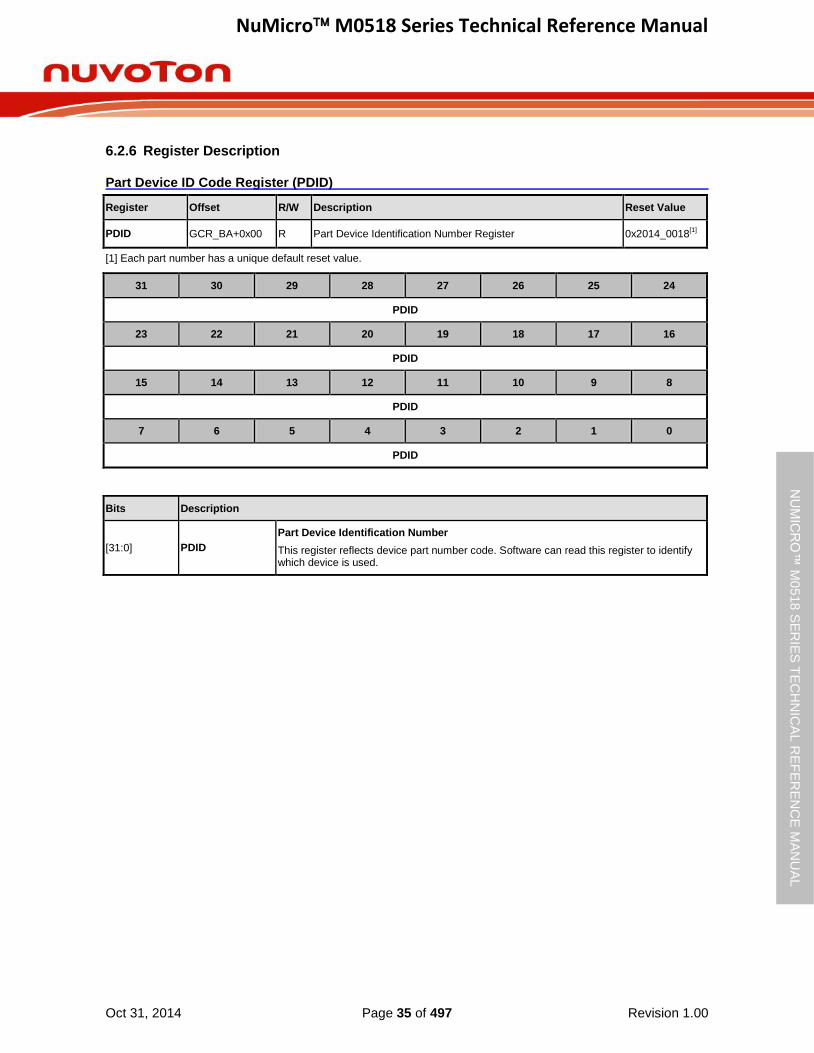
NuMicro M0518 Series Technical Reference Manual
Oct 31, 2014 Page 35 of 497 Revision 1.00
NU
MIC
RO
™ M
0518
SE
RIE
S T
EC
HN
ICA
L R
EF
ER
EN
CE
MA
NU
AL
6.2.6 Register Description
Part Device ID Code Register (PDID)
Register Offset R/W Description Reset Value
PDID GCR_BA+0x00 R Part Device Identification Number Register 0x2014_0018[1]
[1] Each part number has a unique default reset value.
31 30 29 28 27 26 25 24
PDID
23 22 21 20 19 18 17 16
PDID
15 14 13 12 11 10 9 8
PDID
7 6 5 4 3 2 1 0
PDID
Bits Description
[31:0] PDID
Part Device Identification Number
This register reflects device part number code. Software can read this register to identify which device is used.

NuMicro M0518 Series Technical Reference Manual
Oct 31, 2014 Page 36 of 497 Revision 1.00
NU
MIC
RO
™ M
0518
SE
RIE
S T
EC
HN
ICA
L R
EF
ER
EN
CE
MA
NU
AL
System Reset Source Register (RSTSRC)
This register provides specific information for software to identify this chip’s reset source from last operation.
Register Offset R/W Description Reset Value
RSTSRC GCR_BA+0x04 R/W System Reset Source Register 0x0000_00XX
31 30 29 28 27 26 25 24
Reserved
23 22 21 20 19 18 17 16
Reserved
15 14 13 12 11 10 9 8
Reserved
7 6 5 4 3 2 1 0
RSTS_CPU Reserved RSTS_SYS RSTS_BOD RSTS_LVR RSTS_WDT RSTS_RESET RSTS_POR
Bits Description
[31:8] Reserved Reserved.
[7] RSTS_CPU
CPU Reset Flag
The RSTS_CPU flag Is set by hardware if software writes CPU_RST (IPRSTC1[1]) 1 To reset Cortex™-M0 core and flash memory controller (FMC).
0 = No reset from CPU.
1 = Cortex™-M0 CPU core and FMC are reset by software setting CPU_RST (IPRSTC1[1]) to 1.
Note: Write 1 to clear this bit to 0.
[6] Reserved Reserved.
[5] RSTS_SYS
SYS Reset Flag
The RSTS_SYS flag Is set by the “Reset Signal” from the Cortex™-M0 core to indicate the previous reset source.
0 = No reset from Cortex™-M0.
1 = The Cortex™-M0 had issued the reset signal to reset the system by writing 1 to bit SYSRESETREQ (AIRCR[2], Application Interrupt and Reset Control Register, address = 0xE000ED0C) in system control registers of Cortex™-M0 core.
Note: Write 1 to clear this bit to 0.
[4] RSTS_BOD
Brown-Out Detector Reset Flag
The RSTS_BOD flag is set by the “Reset Signal” from the Brown-Out Detector to indicate the previous reset source.
0 = No reset from BOD.
1 = The BOD had issued the reset signal to reset the system.
Note: Write 1 to clear this bit to 0.
[3] RSTS_LVR Low Voltage Reset Flag
The RSTS_LVR flag is set by the “Reset Signal” from the Low-Voltage-Reset controller to
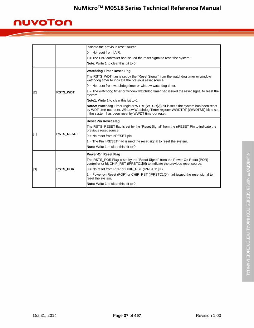
NuMicro M0518 Series Technical Reference Manual
Oct 31, 2014 Page 37 of 497 Revision 1.00
NU
MIC
RO
™ M
0518
SE
RIE
S T
EC
HN
ICA
L R
EF
ER
EN
CE
MA
NU
AL
indicate the previous reset source.
0 = No reset from LVR.
1 = The LVR controller had issued the reset signal to reset the system.
Note: Write 1 to clear this bit to 0.
[2] RSTS_WDT
Watchdog Timer Reset Flag
The RSTS_WDT flag is set by the “Reset Signal” from the watchdog timer or window watchdog timer to indicate the previous reset source.
0 = No reset from watchdog timer or window watchdog timer.
1 = The watchdog timer or window watchdog timer had issued the reset signal to reset the system.
Note1: Write 1 to clear this bit to 0.
Note2: Watchdog Timer register WTRF (WTCR[2]) bit is set if the system has been reset by WDT time-out reset. Window Watchdog Timer register WWDTRF (WWDTSR) bit is set if the system has been reset by WWDT time-out reset.
[1] RSTS_RESET
Reset Pin Reset Flag
The RSTS_RESET flag is set by the “Reset Signal” from the nRESET Pin to indicate the previous reset source.
0 = No reset from nRESET pin.
1 = The Pin nRESET had issued the reset signal to reset the system.
Note: Write 1 to clear this bit to 0.
[0] RSTS_POR
Power-On Reset Flag
The RSTS_POR Flag is set by the “Reset Signal” from the Power-On Reset (POR) vontroller or bit CHIP_RST (IPRSTC1[0]) to indicate the previous reset source.
0 = No reset from POR or CHIP_RST (IPRSTC1[0]).
1 = Power-on Reset (POR) or CHIP_RST (IPRSTC1[0]) had issued the reset signal to reset the system.
Note: Write 1 to clear this bit to 0.
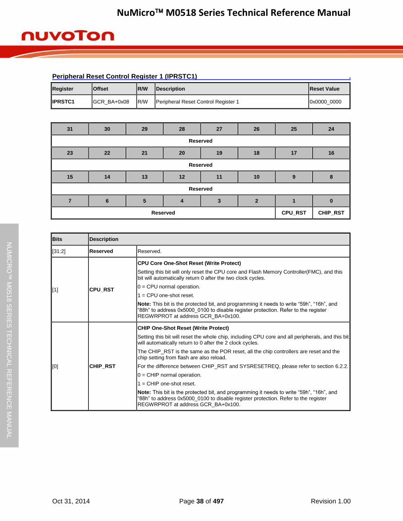
NuMicro M0518 Series Technical Reference Manual
Oct 31, 2014 Page 38 of 497 Revision 1.00
NU
MIC
RO
™ M
0518
SE
RIE
S T
EC
HN
ICA
L R
EF
ER
EN
CE
MA
NU
AL
Peripheral Reset Control Register 1 (IPRSTC1) .
Register Offset R/W Description Reset Value
IPRSTC1 GCR_BA+0x08 R/W Peripheral Reset Control Register 1 0x0000_0000
31 30 29 28 27 26 25 24
Reserved
23 22 21 20 19 18 17 16
Reserved
15 14 13 12 11 10 9 8
Reserved
7 6 5 4 3 2 1 0
Reserved CPU_RST CHIP_RST
Bits Description
[31:2] Reserved Reserved.
[1] CPU_RST
CPU Core One-Shot Reset (Write Protect)
Setting this bit will only reset the CPU core and Flash Memory Controller(FMC), and this bit will automatically return 0 after the two clock cycles.
0 = CPU normal operation.
1 = CPU one-shot reset.
Note: This bit is the protected bit, and programming it needs to write “59h”, “16h”, and “88h” to address 0x5000_0100 to disable register protection. Refer to the register REGWRPROT at address GCR_BA+0x100.
[0] CHIP_RST
CHIP One-Shot Reset (Write Protect)
Setting this bit will reset the whole chip, including CPU core and all peripherals, and this bit will automatically return to 0 after the 2 clock cycles.
The CHIP_RST is the same as the POR reset, all the chip controllers are reset and the chip setting from flash are also reload.
For the difference between CHIP_RST and SYSRESETREQ, please refer to section 6.2.2.
0 = CHIP normal operation.
1 = CHIP one-shot reset.
Note: This bit is the protected bit, and programming it needs to write “59h”, “16h”, and “88h” to address 0x5000_0100 to disable register protection. Refer to the register REGWRPROT at address GCR_BA+0x100.
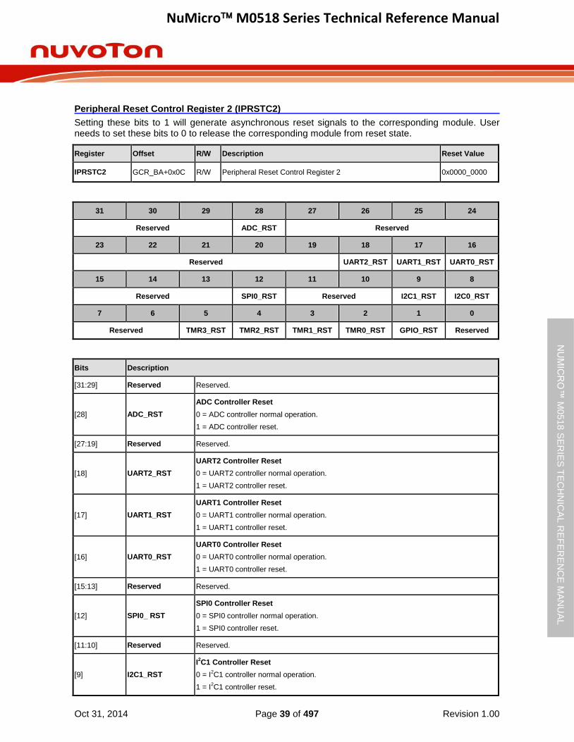
NuMicro M0518 Series Technical Reference Manual
Oct 31, 2014 Page 39 of 497 Revision 1.00
NU
MIC
RO
™ M
0518
SE
RIE
S T
EC
HN
ICA
L R
EF
ER
EN
CE
MA
NU
AL
Peripheral Reset Control Register 2 (IPRSTC2)
Setting these bits to 1 will generate asynchronous reset signals to the corresponding module. User needs to set these bits to 0 to release the corresponding module from reset state.
Register Offset R/W Description Reset Value
IPRSTC2 GCR_BA+0x0C R/W Peripheral Reset Control Register 2 0x0000_0000
31 30 29 28 27 26 25 24
Reserved ADC_RST Reserved
23 22 21 20 19 18 17 16
Reserved UART2_RST UART1_RST UART0_RST
15 14 13 12 11 10 9 8
Reserved SPI0_RST Reserved I2C1_RST I2C0_RST
7 6 5 4 3 2 1 0
Reserved TMR3_RST TMR2_RST TMR1_RST TMR0_RST GPIO_RST Reserved
Bits Description
[31:29] Reserved Reserved.
[28] ADC_RST
ADC Controller Reset
0 = ADC controller normal operation.
1 = ADC controller reset.
[27:19] Reserved Reserved.
[18] UART2_RST
UART2 Controller Reset
0 = UART2 controller normal operation.
1 = UART2 controller reset.
[17] UART1_RST
UART1 Controller Reset
0 = UART1 controller normal operation.
1 = UART1 controller reset.
[16] UART0_RST
UART0 Controller Reset
0 = UART0 controller normal operation.
1 = UART0 controller reset.
[15:13] Reserved Reserved.
[12] SPI0_ RST
SPI0 Controller Reset
0 = SPI0 controller normal operation.
1 = SPI0 controller reset.
[11:10] Reserved Reserved.
[9] I2C1_RST
I2C1 Controller Reset
0 = I2C1 controller normal operation.
1 = I2C1 controller reset.

NuMicro M0518 Series Technical Reference Manual
Oct 31, 2014 Page 40 of 497 Revision 1.00
NU
MIC
RO
™ M
0518
SE
RIE
S T
EC
HN
ICA
L R
EF
ER
EN
CE
MA
NU
AL
[8] I2C0_RST
I2C0 Controller Reset
0 = I2C0 controller normal operation.
1 = I2C0 controller reset.
[7:6] Reserved Reserved.
[5] TMR3_RST
Timer3 Controller Reset
0 = Timer3 controller normal operation.
1 = Timer3 controller reset.
[4] TMR2_RST
Timer2 Controller Reset
0 = Timer2 controller normal operation.
1 = Timer2 controller reset.
[3] TMR1_RST
Timer1 Controller Reset
0 = Timer1 controller normal operation.
1 = Timer1 controller reset.
[2] TMR0_RST
Timer0 Controller Reset
0 = Timer0 controller normal operation.
1 = Timer0 controller reset.
[1] GPIO_RST
GPIO Controller Reset
0 = GPIO controller normal operation.
1 = GPIO controller reset.
[0] Reserved Reserved.
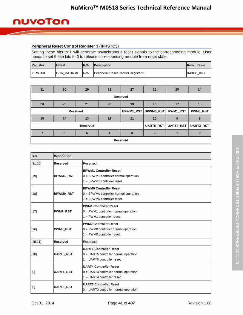
NuMicro M0518 Series Technical Reference Manual
Oct 31, 2014 Page 41 of 497 Revision 1.00
NU
MIC
RO
™ M
0518
SE
RIE
S T
EC
HN
ICA
L R
EF
ER
EN
CE
MA
NU
AL
Peripheral Reset Control Register 3 (IPRSTC3)
Setting these bits to 1 will generate asynchronous reset signals to the corresponding module. User needs to set these bits to 0 to release corresponding module from reset state.
Register Offset R/W Description Reset Value
IPRSTC3 GCR_BA+0x10 R/W Peripheral Reset Control Register 3 0x0000_0000
31 30 29 28 27 26 25 24
Reserved
23 22 21 20 19 18 17 16
Reserved BPWM1_RST BPWM0_RST PWM1_RST PWM0_RST
15 14 13 12 11 10 9 8
Reserved UART5_RST UART4_RST UART3_RST
7 6 5 4 3 2 1 0
Reserved
Bits Description
[31:20] Reserved Reserved.
[19] BPWM1_RST
BPWM1 Controller Reset
0 = BPWM1 controller normal operation.
1 = BPWM1 controller reset.
[18] BPWM0_RST
BPWM0 Controller Reset
0 = BPWM0 controller normal operation.
1 = BPWM0 controller reset.
[17] PWM1_RST
PWM1 Controller Reset
0 = PWM1 controller normal operation.
1 = PWM1 controller reset.
[16] PWM0_RST
PWM0 Controller Reset
0 = PWM0 controller normal operation.
1 = PWM0 controller reset.
[15:11] Reserved Reserved.
[10] UART5_RST
UART5 Controller Reset
0 = UART5 controller normal operation.
1 = UART5 controller reset.
[9] UART4_RST
UART4 Controller Reset
0 = UART4 controller normal operation.
1 = UART4 controller reset.
[8] UART3_RST UART3 Controller Reset
0 = UART3 controller normal operation.
NuMicro M0518 Series Technical Reference Manual
Oct 31, 2014 Page 42 of 497 Revision 1.00
NU
MIC
RO
™ M
0518
SE
RIE
S T
EC
HN
ICA
L R
EF
ER
EN
CE
MA
NU
AL
1 = UART3 controller reset.
[7:0] Reserved Reserved.

NuMicro M0518 Series Technical Reference Manual
Oct 31, 2014 Page 43 of 497 Revision 1.00
NU
MIC
RO
™ M
0518
SE
RIE
S T
EC
HN
ICA
L R
EF
ER
EN
CE
MA
NU
AL
Brown-out Detector Control Register (BODCR)
Partial of the BODCR control registers values are initiated by the flash configuration and partial bits are write-protected bit. Programming write-protected bits needs to write “59h”, “16h”, “88h” to address 0x5000_0100 to disable register protection. Refer to the register REGWRPROT at address GCR_BA+0x100.
Register Offset R/W Description Reset Value
BODCR GCR_BA+0x18 R/W Brown-out Detector Control Register 0x0000_038X
31 30 29 28 27 26 25 24
Reserved
23 22 21 20 19 18 17 16
Reserved
15 14 13 12 11 10 9 8
Reserved LVRDGSEL Reserved BODDGSEL
7 6 5 4 3 2 1 0
LVR_EN BOD_OUT BOD_LPM BOD_INTF BOD_RSTEN BOD_VL BOD_EN
Bits Description
[31:15] Reserved Reserved.
[14:12] LVRDGSEL
LVR Output De-Glitch Time Select (Write Protect)
000 = Without de-glitch function.
001 = 4 system clock (HCLK).
010 = 8 system clock (HCLK).
011 = 16 system clock (HCLK).
100 = 32 system clock (HCLK).
101 = 64 system clock (HCLK).
110 = 128 system clock (HCLK).
111 = 256 system clock (HCLK).
Note: This bit is the protected bit, and programming it needs to write “59h”, “16h”, and “88h” to address 0x5000_0100 to disable register protection. Refer to the register REGWRPROT at address GCR_BA+0x100.
[11] Reserved Reserved.
[10:8] BODDGSEL
Brown-Out Detector Output De-Glitch Time Select (Write Protect)
000 = BOD output is sampled by RC10K clock.
001 = 4 system clock (HCLK).
010 = 8 system clock (HCLK).
011 = 16 system clock (HCLK).
100 = 32 system clock (HCLK).
101 = 64 system clock (HCLK).
110 = 128 system clock (HCLK).
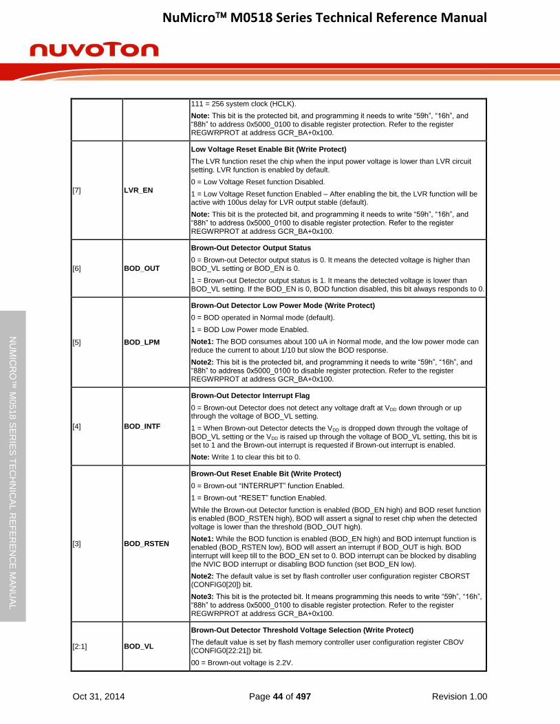
NuMicro M0518 Series Technical Reference Manual
Oct 31, 2014 Page 44 of 497 Revision 1.00
NU
MIC
RO
™ M
0518
SE
RIE
S T
EC
HN
ICA
L R
EF
ER
EN
CE
MA
NU
AL
111 = 256 system clock (HCLK).
Note: This bit is the protected bit, and programming it needs to write “59h”, “16h”, and “88h” to address 0x5000_0100 to disable register protection. Refer to the register REGWRPROT at address GCR_BA+0x100.
[7] LVR_EN
Low Voltage Reset Enable Bit (Write Protect)
The LVR function reset the chip when the input power voltage is lower than LVR circuit setting. LVR function is enabled by default.
0 = Low Voltage Reset function Disabled.
1 = Low Voltage Reset function Enabled – After enabling the bit, the LVR function will be active with 100us delay for LVR output stable (default).
Note: This bit is the protected bit, and programming it needs to write “59h”, “16h”, and “88h” to address 0x5000_0100 to disable register protection. Refer to the register REGWRPROT at address GCR_BA+0x100.
[6] BOD_OUT
Brown-Out Detector Output Status
0 = Brown-out Detector output status is 0. It means the detected voltage is higher than BOD_VL setting or BOD_EN is 0.
1 = Brown-out Detector output status is 1. It means the detected voltage is lower than BOD_VL setting. If the BOD_EN is 0, BOD function disabled, this bit always responds to 0.
[5] BOD_LPM
Brown-Out Detector Low Power Mode (Write Protect)
0 = BOD operated in Normal mode (default).
1 = BOD Low Power mode Enabled.
Note1: The BOD consumes about 100 uA in Normal mode, and the low power mode can reduce the current to about 1/10 but slow the BOD response.
Note2: This bit is the protected bit, and programming it needs to write “59h”, “16h”, and “88h” to address 0x5000_0100 to disable register protection. Refer to the register REGWRPROT at address GCR_BA+0x100.
[4] BOD_INTF
Brown-Out Detector Interrupt Flag
0 = Brown-out Detector does not detect any voltage draft at VDD down through or up through the voltage of BOD_VL setting.
1 = When Brown-out Detector detects the VDD is dropped down through the voltage of BOD_VL setting or the VDD is raised up through the voltage of BOD_VL setting, this bit is set to 1 and the Brown-out interrupt is requested if Brown-out interrupt is enabled.
Note: Write 1 to clear this bit to 0.
[3] BOD_RSTEN
Brown-Out Reset Enable Bit (Write Protect)
0 = Brown-out “INTERRUPT” function Enabled.
1 = Brown-out “RESET” function Enabled.
While the Brown-out Detector function is enabled (BOD_EN high) and BOD reset function is enabled (BOD_RSTEN high), BOD will assert a signal to reset chip when the detected voltage is lower than the threshold (BOD_OUT high).
Note1: While the BOD function is enabled (BOD_EN high) and BOD interrupt function is enabled (BOD_RSTEN low), BOD will assert an interrupt if BOD_OUT is high. BOD interrupt will keep till to the BOD_EN set to 0. BOD interrupt can be blocked by disabling the NVIC BOD interrupt or disabling BOD function (set BOD_EN low).
Note2: The default value is set by flash controller user configuration register CBORST (CONFIG0[20]) bit.
Note3: This bit is the protected bit. It means programming this needs to write “59h”, “16h”, “88h” to address 0x5000_0100 to disable register protection. Refer to the register REGWRPROT at address GCR_BA+0x100.
[2:1] BOD_VL
Brown-Out Detector Threshold Voltage Selection (Write Protect)
The default value is set by flash memory controller user configuration register CBOV (CONFIG0[22:21]) bit.
00 = Brown-out voltage is 2.2V.
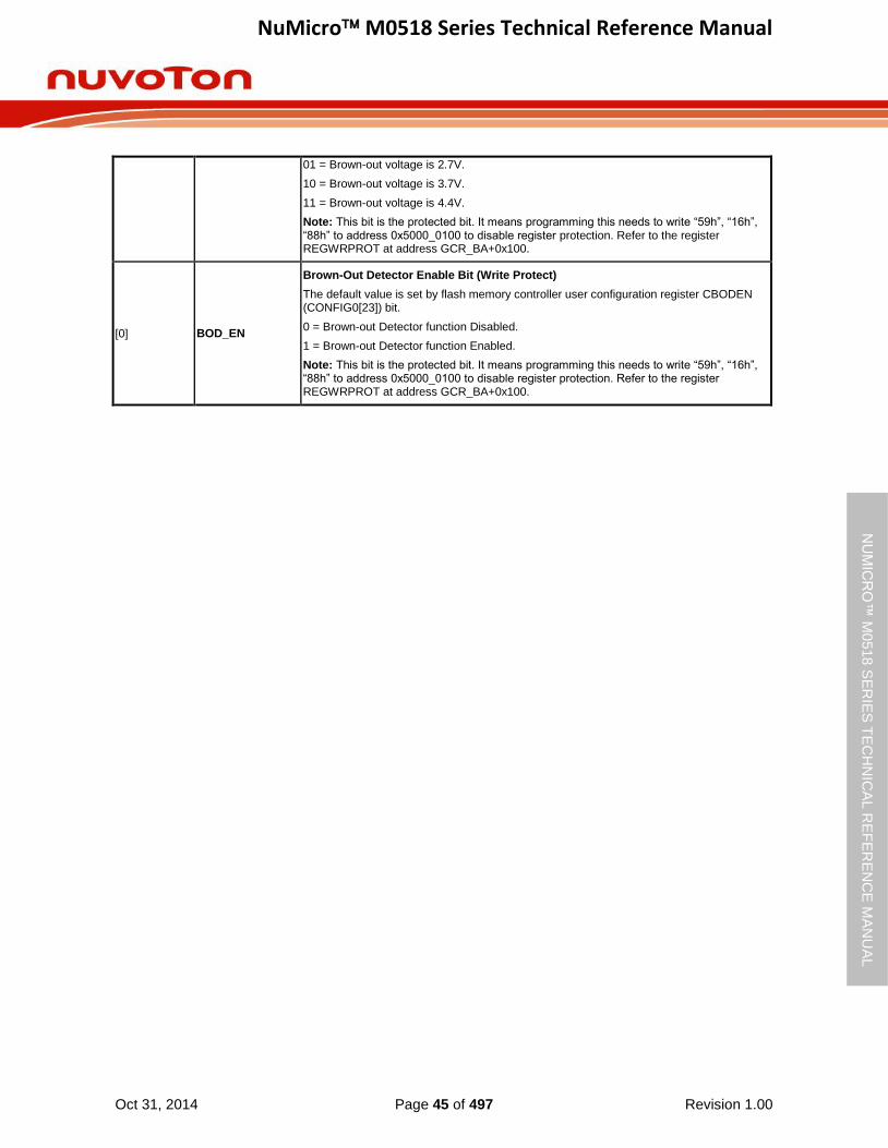
NuMicro M0518 Series Technical Reference Manual
Oct 31, 2014 Page 45 of 497 Revision 1.00
NU
MIC
RO
™ M
0518
SE
RIE
S T
EC
HN
ICA
L R
EF
ER
EN
CE
MA
NU
AL
01 = Brown-out voltage is 2.7V.
10 = Brown-out voltage is 3.7V.
11 = Brown-out voltage is 4.4V.
Note: This bit is the protected bit. It means programming this needs to write “59h”, “16h”, “88h” to address 0x5000_0100 to disable register protection. Refer to the register REGWRPROT at address GCR_BA+0x100.
[0] BOD_EN
Brown-Out Detector Enable Bit (Write Protect)
The default value is set by flash memory controller user configuration register CBODEN (CONFIG0[23]) bit.
0 = Brown-out Detector function Disabled.
1 = Brown-out Detector function Enabled.
Note: This bit is the protected bit. It means programming this needs to write “59h”, “16h”, “88h” to address 0x5000_0100 to disable register protection. Refer to the register REGWRPROT at address GCR_BA+0x100.
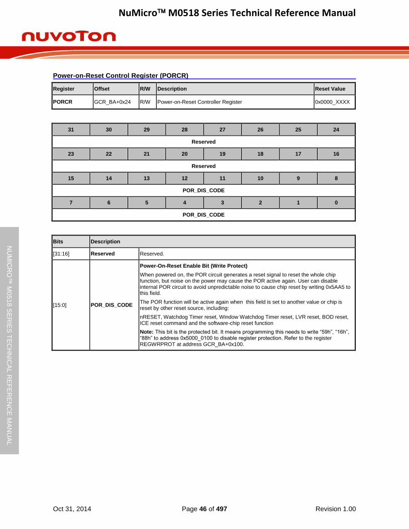
NuMicro M0518 Series Technical Reference Manual
Oct 31, 2014 Page 46 of 497 Revision 1.00
NU
MIC
RO
™ M
0518
SE
RIE
S T
EC
HN
ICA
L R
EF
ER
EN
CE
MA
NU
AL
Power-on-Reset Control Register (PORCR)
Register Offset R/W Description Reset Value
PORCR GCR_BA+0x24 R/W Power-on-Reset Controller Register 0x0000_XXXX
31 30 29 28 27 26 25 24
Reserved
23 22 21 20 19 18 17 16
Reserved
15 14 13 12 11 10 9 8
POR_DIS_CODE
7 6 5 4 3 2 1 0
POR_DIS_CODE
Bits Description
[31:16] Reserved Reserved.
[15:0] POR_DIS_CODE
Power-On-Reset Enable Bit (Write Protect)
When powered on, the POR circuit generates a reset signal to reset the whole chip function, but noise on the power may cause the POR active again. User can disable internal POR circuit to avoid unpredictable noise to cause chip reset by writing 0x5AA5 to this field.
The POR function will be active again when this field is set to another value or chip is reset by other reset source, including:
nRESET, Watchdog Timer reset, Window Watchdog Timer reset, LVR reset, BOD reset, ICE reset command and the software-chip reset function
Note: This bit is the protected bit. It means programming this needs to write “59h”, “16h”, “88h” to address 0x5000_0100 to disable register protection. Refer to the register REGWRPROT at address GCR_BA+0x100.
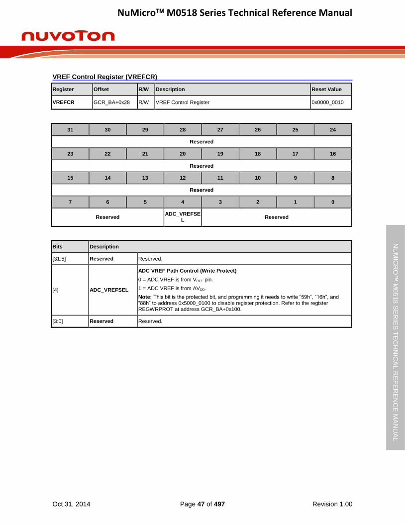
NuMicro M0518 Series Technical Reference Manual
Oct 31, 2014 Page 47 of 497 Revision 1.00
NU
MIC
RO
™ M
0518
SE
RIE
S T
EC
HN
ICA
L R
EF
ER
EN
CE
MA
NU
AL
VREF Control Register (VREFCR)
Register Offset R/W Description Reset Value
VREFCR GCR_BA+0x28 R/W VREF Control Register 0x0000_0010
31 30 29 28 27 26 25 24
Reserved
23 22 21 20 19 18 17 16
Reserved
15 14 13 12 11 10 9 8
Reserved
7 6 5 4 3 2 1 0
Reserved ADC_VREFSE
L Reserved
Bits Description
[31:5] Reserved Reserved.
[4] ADC_VREFSEL
ADC VREF Path Control (Write Protect)
0 = ADC VREF is from VREF pin.
1 = ADC VREF is from AVDD.
Note: This bit is the protected bit, and programming it needs to write “59h”, “16h”, and “88h” to address 0x5000_0100 to disable register protection. Refer to the register REGWRPROT at address GCR_BA+0x100.
[3:0] Reserved Reserved.

NuMicro M0518 Series Technical Reference Manual
Oct 31, 2014 Page 48 of 497 Revision 1.00
NU
MIC
RO
™ M
0518
SE
RIE
S T
EC
HN
ICA
L R
EF
ER
EN
CE
MA
NU
AL
GPIOA Multiple Function Pin and Input Type Control Register (GPA_MFP)
Register Offset R/W Description Reset Value
GPA_MFP GCR_BA+0x30 R/W GPIOA Multiple Function and Input Type Control Register 0x0000_0000
31 30 29 28 27 26 25 24
GPA_TYPE
23 22 21 20 19 18 17 16
GPA_TYPE
15 14 13 12 11 10 9 8
GPA_MFP
7 6 5 4 3 2 1 0
GPA_MFP
Bits Description
[31:16] GPA_TYPEn
Trigger Function Selection
0 = GPIOA[15:0] I/O input Schmitt Trigger function Disabled.
1 = GPIOA[15:0] I/O input Schmitt Trigger function Enabled.
[15] GPA_MFP15
PA.15 Pin Function Selection
Bit GPA_MFP15 determines the PA.15 function.
0 = GPIO function is selected.
1 = PWM0_CH3 function is selected.
[14] GPA_MFP14
PA.14 Pin Function Selection
Bit GPA_MFP14 determines the PA.14 function.
0 = GPIO function is selected.
1 = PWM0_CH2 function is selected.
[13] GPA_MFP13
PA.13 Pin Function Selection
Bits PA13_UR5TXD (ALT_MFP4[9]) and GPA_MFP13 determine the PA.13 function.
(PA13_UR5TXD, GPA_MFP13) value and function mapping is as following list.
(0, 0) = GPIO function is selected.
(0, 1) = PWM0_CH1 function is selected.
(1, 1) = UART5_TXD function is selected.
[12] GPA_MFP12
PA.12 Pin Function Selection
Bits PA12_UR5RXD (ALT_MFP4[8]) and GPA_MFP12 determine the PA.12 function.
(PA12_UR5RXD, GPA_MFP12) value and function mapping is as following list.
(0, 0) = GPIO function is selected.
(0, 1) = PWM0_CH0 function is selected.
(1, 1) = UART5_RXD function is selected.
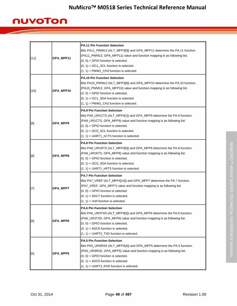
NuMicro M0518 Series Technical Reference Manual
Oct 31, 2014 Page 49 of 497 Revision 1.00
NU
MIC
RO
™ M
0518
SE
RIE
S T
EC
HN
ICA
L R
EF
ER
EN
CE
MA
NU
AL
[11] GPA_MFP11
PA.11 Pin Function Selection
Bits PA11_PWM13 (ALT_MFP3[9]) and GPA_MFP11 determine the PA.11 function.
(PA11_PWM13, GPA_MFP11) value and function mapping is as following list.
(0, 0) = GPIO function is selected.
(0, 1) = I2C1_SCL function is selected.
(1, 1) = PWM1_CH3 function is selected.
[10] GPA_MFP10
PA.10 Pin Function Selection
Bits PA10_PWM12 (ALT_MFP3[8]) and GPA_MFP10 determine the PA.10 function.
(PA10_PWM12, GPA_MFP10) value and function mapping is as following list.
(0, 0) = GPIO function is selected.
(0, 1) = I2C1_SDA function is selected.
(1, 1) = PWM1_CH2 function is selected.
[9] GPA_MFP9
PA.9 Pin Function Selection
Bits PA9_UR1CTS (ALT_MFP4[1]) and GPA_MFP9 determine the PA.9 function.
(PA9_UR1CTS, GPA_MFP9) value and function mapping is as following list.
(0, 0) = GPIO function is selected.
(0, 1) = I2C0_SCL function is selected.
(1, 1) = UART1_nCTS function is selected.
[8] GPA_MFP8
PA.8 Pin Function Selection
Bits PA8_UR1RTS (ALT_MFP4[0]) and GPA_MFP8 determine the PA.8 function.
(PA8_UR1RTS, GPA_MFP8) value and function mapping is as following list.
(0, 0) = GPIO function is selected.
(0, 1) = I2C0_SDA function is selected.
(1, 1) = UART1_nRTS function is selected.
[7] GPA_MFP7
PA.7 Pin Function Selection
Bits PA7_VREF (ALT_MFP4[14]) and GPA_MFP7 determine the PA.7 function.
(PA7_VREF, GPA_MFP7) value and function mapping is as following list.
(0, 0) = GPIO function is selected.
(0, 1) = ADC7 function is selected.
(1, 1) = Vref function is selected.
[6] GPA_MFP6
PA.6 Pin Function Selection
Bits PA6_UR3TXD (ALT_MFP4[5]) and GPA_MFP6 determine the PA.6 function.
(PA6_UR3TXD, GPA_MFP6) value and function mapping is as following list.
(0, 0) = GPIO function is selected.
(0, 1) = ADC6 function is selected.
(1, 1) = UART3_TXD function is selected.
[5] GPA_MFP5
PA.5 Pin Function Selection
Bits PA5_UR3RXD (ALT_MFP4[4]) and GPA_MFP5 determine the PA.5 function.
(PA5_UR3RXD, GPA_MFP5) value and function mapping is as following list.
(0, 0) = GPIO function is selected.
(0, 1) = ADC5 function is selected.
(1, 1) = UART3_RXD function is selected.
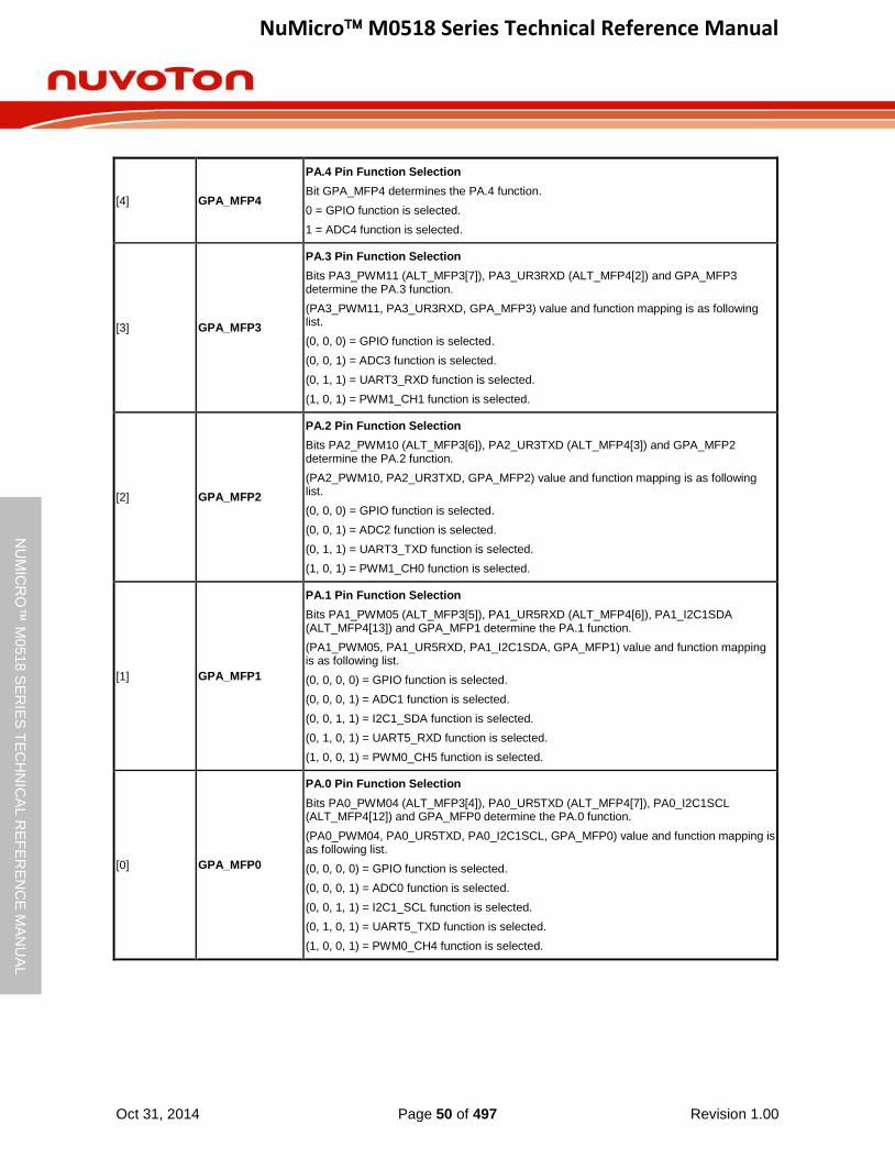
NuMicro M0518 Series Technical Reference Manual
Oct 31, 2014 Page 50 of 497 Revision 1.00
NU
MIC
RO
™ M
0518
SE
RIE
S T
EC
HN
ICA
L R
EF
ER
EN
CE
MA
NU
AL
[4] GPA_MFP4
PA.4 Pin Function Selection
Bit GPA_MFP4 determines the PA.4 function.
0 = GPIO function is selected.
1 = ADC4 function is selected.
[3] GPA_MFP3
PA.3 Pin Function Selection
Bits PA3_PWM11 (ALT_MFP3[7]), PA3_UR3RXD (ALT_MFP4[2]) and GPA_MFP3 determine the PA.3 function.
(PA3_PWM11, PA3_UR3RXD, GPA_MFP3) value and function mapping is as following list.
(0, 0, 0) = GPIO function is selected.
(0, 0, 1) = ADC3 function is selected.
(0, 1, 1) = UART3_RXD function is selected.
(1, 0, 1) = PWM1_CH1 function is selected.
[2] GPA_MFP2
PA.2 Pin Function Selection
Bits PA2_PWM10 (ALT_MFP3[6]), PA2_UR3TXD (ALT_MFP4[3]) and GPA_MFP2 determine the PA.2 function.
(PA2_PWM10, PA2_UR3TXD, GPA_MFP2) value and function mapping is as following list.
(0, 0, 0) = GPIO function is selected.
(0, 0, 1) = ADC2 function is selected.
(0, 1, 1) = UART3_TXD function is selected.
(1, 0, 1) = PWM1_CH0 function is selected.
[1] GPA_MFP1
PA.1 Pin Function Selection
Bits PA1_PWM05 (ALT_MFP3[5]), PA1_UR5RXD (ALT_MFP4[6]), PA1_I2C1SDA (ALT_MFP4[13]) and GPA_MFP1 determine the PA.1 function.
(PA1_PWM05, PA1_UR5RXD, PA1_I2C1SDA, GPA_MFP1) value and function mapping is as following list.
(0, 0, 0, 0) = GPIO function is selected.
(0, 0, 0, 1) = ADC1 function is selected.
(0, 0, 1, 1) = I2C1_SDA function is selected.
(0, 1, 0, 1) = UART5_RXD function is selected.
(1, 0, 0, 1) = PWM0_CH5 function is selected.
[0] GPA_MFP0
PA.0 Pin Function Selection
Bits PA0_PWM04 (ALT_MFP3[4]), PA0_UR5TXD (ALT_MFP4[7]), PA0_I2C1SCL (ALT_MFP4[12]) and GPA_MFP0 determine the PA.0 function.
(PA0_PWM04, PA0_UR5TXD, PA0_I2C1SCL, GPA_MFP0) value and function mapping is as following list.
(0, 0, 0, 0) = GPIO function is selected.
(0, 0, 0, 1) = ADC0 function is selected.
(0, 0, 1, 1) = I2C1_SCL function is selected.
(0, 1, 0, 1) = UART5_TXD function is selected.
(1, 0, 0, 1) = PWM0_CH4 function is selected.

NuMicro M0518 Series Technical Reference Manual
Oct 31, 2014 Page 51 of 497 Revision 1.00
NU
MIC
RO
™ M
0518
SE
RIE
S T
EC
HN
ICA
L R
EF
ER
EN
CE
MA
NU
AL
GPIOB Multiple Function Pin and Input Type Control Register (GPB_MFP)
Register Offset R/W Description Reset Value
GPB_MFP GCR_BA+0x34 R/W GPIOB Multiple Function and Input Type Control Register 0x0000_0000
31 30 29 28 27 26 25 24
GPB_TYPE
23 22 21 20 19 18 17 16
GPB_TYPE
15 14 13 12 11 10 9 8
GPB_MFP
7 6 5 4 3 2 1 0
GPB_MFP
Bits Description
[31:16] GPB_TYPEn
Trigger Function Selection
0 = GPIOB[15:0] I/O input Schmitt Trigger function Disabled.
1 = GPIOB[15:0] I/O input Schmitt Trigger function Enabled.
[15] GPB_MFP15
PB.15 Pin Function Selection
Bits PB15_BPWM15 (ALT_MFP3[23]), PB15_T0EX (ALT_MFP[24]), PB15_TM0 (ALT_MFP2[2]) and GPB_MFP15 determine the PB.15 function.
(PB15_BPWM15, PB15_T0EX, PB15_TM0, GPB_MFP15) value and function mapping is as following list.
(0, 0, 0, 0) = GPIO function is selected.
(0, 0, 0, 1) = INT1 function is selected.
(0, 0, 1, 1) = TM0 function is selected.
(0, 1, 0, 1) = TM0_EXT function is selected.
(1, 0, 1, 1) = BPWM1_CH5 function is selected.
[14] GPB_MFP14
PB.14 Pin Function Selection
Bit GPB_MFP14 determines the PB.14 function.
0 = GPIO function is selected.
1 = INT0 function is selected.
[13] Reserved Reserved.
[12] GPB_MFP12
PB.12 Pin Function Selection
Bits PB12_BPWM13 (ALT_MFP3[21]) and GPB_MFP12 determine the PB.12 function.
(PB12_BPWM13, GPB_MFP12) value and function mapping is as following list.
(0, 0) = GPIO function is selected.
(0, 1) = CLKO function is selected.
(1, 1) = BPWM1_CH3 function is selected.
[11] GPB_MFP11 PB.11 Pin Function Selection
Bits PB11_PWM04 (ALT_MFP3[24]) and GPB_MFP11 determine the PB.11 function.
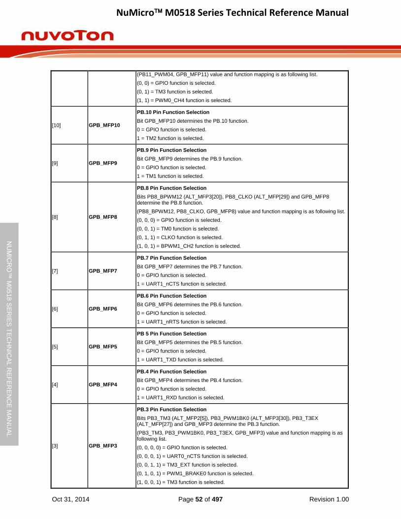
NuMicro M0518 Series Technical Reference Manual
Oct 31, 2014 Page 52 of 497 Revision 1.00
NU
MIC
RO
™ M
0518
SE
RIE
S T
EC
HN
ICA
L R
EF
ER
EN
CE
MA
NU
AL
(PB11_PWM04, GPB_MFP11) value and function mapping is as following list.
(0, 0) = GPIO function is selected.
(0, 1) = TM3 function is selected.
(1, 1) = PWM0_CH4 function is selected.
[10] GPB_MFP10
PB.10 Pin Function Selection
Bit GPB_MFP10 determines the PB.10 function.
0 = GPIO function is selected.
1 = TM2 function is selected.
[9] GPB_MFP9
PB.9 Pin Function Selection
Bit GPB_MFP9 determines the PB.9 function.
0 = GPIO function is selected.
1 = TM1 function is selected.
[8] GPB_MFP8
PB.8 Pin Function Selection
Bits PB8_BPWM12 (ALT_MFP3[20]), PB8_CLKO (ALT_MFP[29]) and GPB_MFP8 determine the PB.8 function.
(PB8_BPWM12, PB8_CLKO, GPB_MFP8) value and function mapping is as following list.
(0, 0, 0) = GPIO function is selected.
(0, 0, 1) = TM0 function is selected.
(0, 1, 1) = CLKO function is selected.
(1, 0, 1) = BPWM1_CH2 function is selected.
[7] GPB_MFP7
PB.7 Pin Function Selection
Bit GPB_MFP7 determines the PB.7 function.
0 = GPIO function is selected.
1 = UART1_nCTS function is selected.
[6] GPB_MFP6
PB.6 Pin Function Selection
Bit GPB_MFP6 determines the PB.6 function.
0 = GPIO function is selected.
1 = UART1_nRTS function is selected.
[5] GPB_MFP5
PB 5 Pin Function Selection
Bit GPB_MFP5 determines the PB.5 function.
0 = GPIO function is selected.
1 = UART1_TXD function is selected.
[4] GPB_MFP4
PB.4 Pin Function Selection
Bit GPB_MFP4 determines the PB.4 function.
0 = GPIO function is selected.
1 = UART1_RXD function is selected.
[3] GPB_MFP3
PB.3 Pin Function Selection
Bits PB3_TM3 (ALT_MFP2[5]), PB3_PWM1BK0 (ALT_MFP3[30]), PB3_T3EX (ALT_MFP[27]) and GPB_MFP3 determine the PB.3 function.
(PB3_TM3, PB3_PWM1BK0, PB3_T3EX, GPB_MFP3) value and function mapping is as following list.
(0, 0, 0, 0) = GPIO function is selected.
(0, 0, 0, 1) = UART0_nCTS function is selected.
(0, 0, 1, 1) = TM3_EXT function is selected.
(0, 1, 0, 1) = PWM1_BRAKE0 function is selected.
(1, 0, 0, 1) = TM3 function is selected.
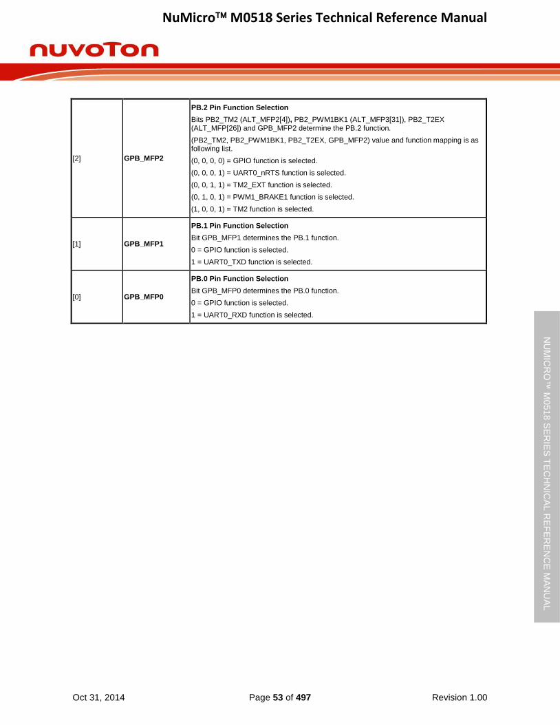
NuMicro M0518 Series Technical Reference Manual
Oct 31, 2014 Page 53 of 497 Revision 1.00
NU
MIC
RO
™ M
0518
SE
RIE
S T
EC
HN
ICA
L R
EF
ER
EN
CE
MA
NU
AL
[2] GPB_MFP2
PB.2 Pin Function Selection
Bits PB2_TM2 (ALT_MFP2[4]), PB2_PWM1BK1 (ALT_MFP3[31]), PB2_T2EX (ALT_MFP[26]) and GPB_MFP2 determine the PB.2 function.
(PB2_TM2, PB2_PWM1BK1, PB2_T2EX, GPB_MFP2) value and function mapping is as following list.
(0, 0, 0, 0) = GPIO function is selected.
(0, 0, 0, 1) = UART0_nRTS function is selected.
(0, 0, 1, 1) = TM2_EXT function is selected.
(0, 1, 0, 1) = PWM1_BRAKE1 function is selected.
(1, 0, 0, 1) = TM2 function is selected.
[1] GPB_MFP1
PB.1 Pin Function Selection
Bit GPB_MFP1 determines the PB.1 function.
0 = GPIO function is selected.
1 = UART0_TXD function is selected.
[0] GPB_MFP0
PB.0 Pin Function Selection
Bit GPB_MFP0 determines the PB.0 function.
0 = GPIO function is selected.
1 = UART0_RXD function is selected.

NuMicro M0518 Series Technical Reference Manual
Oct 31, 2014 Page 54 of 497 Revision 1.00
NU
MIC
RO
™ M
0518
SE
RIE
S T
EC
HN
ICA
L R
EF
ER
EN
CE
MA
NU
AL
GPIOC Multiple Function Pin and input Type Control Register (GPC_MFP)
Register Offset R/W Description Reset Value
GPC_MFP GCR_BA+0x38 R/W GPIOC Multiple Function and Input Type Control Register 0x0000_0000
31 30 29 28 27 26 25 24
GPC_TYPE
23 22 21 20 19 18 17 16
GPC_TYPE
15 14 13 12 11 10 9 8
GPC_MFP
7 6 5 4 3 2 1 0
GPC_MFP
Bits Description
[31:16] GPC_TYPEn
Trigger Function Selection
0 = GPIOC[15:0] I/O input Schmitt Trigger function Disabled.
1 = GPIOC[15:0] I/O input Schmitt Trigger function Enabled.
[15:12] Reserved Reserved.
[11] GPC_MFP11
PC.11 Pin Function Selection
Bit GPC_MFP11 determines the PC.11 function.
0 = GPIO function is selected.
1 = PWM1_BRAKE1 function is selected.
[10] GPC_MFP10
PC.10 Pin Function Selection
Bit GPC_MFP10 determines the PC.10 function.
0 = GPIO function is selected.
1 = PWM1_BRAKE0 function is selected.
[9] GPC_MFP9
PC.9 Pin Function Selection
Bit GPC_MFP9 determines the PC.9 function.
0 = GPIO function is selected.
1 = PWM0_BRAKE1 function is selected.
[8] GPC_MFP8
PC.8 Pin Function Selection
Bit GPC_MFP8 determines the PC.8 function.
0 = GPIO function is selected.
1 = PWM0_BRAKE0 function is selected.
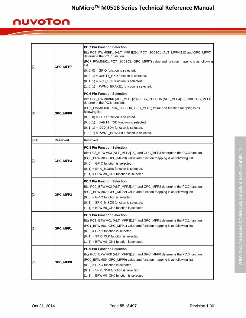
NuMicro M0518 Series Technical Reference Manual
Oct 31, 2014 Page 55 of 497 Revision 1.00
NU
MIC
RO
™ M
0518
SE
RIE
S T
EC
HN
ICA
L R
EF
ER
EN
CE
MA
NU
AL
[7] GPC_MFP7
PC.7 Pin Function Selection
Bits PC7_PWM0BK1 (ALT_MFP3[29]), PC7_I2C0SCL (ALT_MFP4[11]) and GPC_MFP7 determine the PC.7 function.
(PC7_PWM0BK1, PC7_I2C0SCL, GPC_MFP7) value and function mapping is as following list.
(0, 0, 0) = GPIO function is selected.
(0, 0, 1) = UART4_RXD function is selected.
(0, 1, 1) = I2C0_SCL function is selected.
(1, 0, 1) = PWM0_BRAKE1 function is selected.
[6] GPC_MFP6
PC.6 Pin Function Selection
Bits PC6_PWM0BK0 (ALT_MFP3[28]), PC6_I2C0SDA (ALT_MFP4[10]) and GPC_MFP6 determine the PC.6 function.
(PC6_PWM0BK0, PC6_I2C0SDA, GPC_MFP6) value and function mapping is as following list.
(0, 0, 0) = GPIO function is selected.
(0, 0, 1) = UART4_TXD function is selected.
(0, 1, 1) = I2C0_SDA function is selected.
(1, 0, 1) = PWM0_BRAKE0 function is selected.
[5:4] Reserved Reserved.
[3] GPC_MFP3
PC.3 Pin Function Selection
Bits PC3_BPWM03 (ALT_MFP3[15]) and GPC_MFP3 determine the PC.3 function.
(PC3_BPWM03, GPC_MFP3) value and function mapping is as following list.
(0, 0) = GPIO function is selected.
(0, 1) = SPI0_MOSI0 function is selected.
(1, 1) = BPWM0_CH3 function is selected.
[2] GPC_MFP2
PC.2 Pin Function Selection
Bits PC2_BPWM02 (ALT_MFP3[14]) and GPC_MFP2 determine the PC.2 function.
(PC2_BPWM02, GPC_MFP2) value and function mapping is as following list.
(0, 0) = GPIO function is selected.
(0, 1) = SPI0_MISO0 function is selected.
(1, 1) = BPWM0_CH2 function is selected.
[1] GPC_MFP1
PC.1 Pin Function Selection
Bits PC1_BPWM01 (ALT_MFP3[13]) and GPC_MFP1 determine the PC.1 function.
(PC1_BPWM01, GPC_MFP1) value and function mapping is as following list.
(0, 0) = GPIO function is selected.
(0, 1) = SPI0_CLK function is selected.
(1, 1) = BPWM0_CH1 function is selected.
[0] GPC_MFP0
PC.0 Pin Function Selection
Bits PC0_BPWM00 (ALT_MFP3[12]) and GPC_MFP0 determine the PC.0 function.
(PC0_BPWM00, GPC_MFP0) value and function mapping is as following list.
(0, 0) = GPIO function is selected.
(0, 1) = SPI0_SS0 function is selected.
(1, 1) = BPWM0_CH0 function is selected.
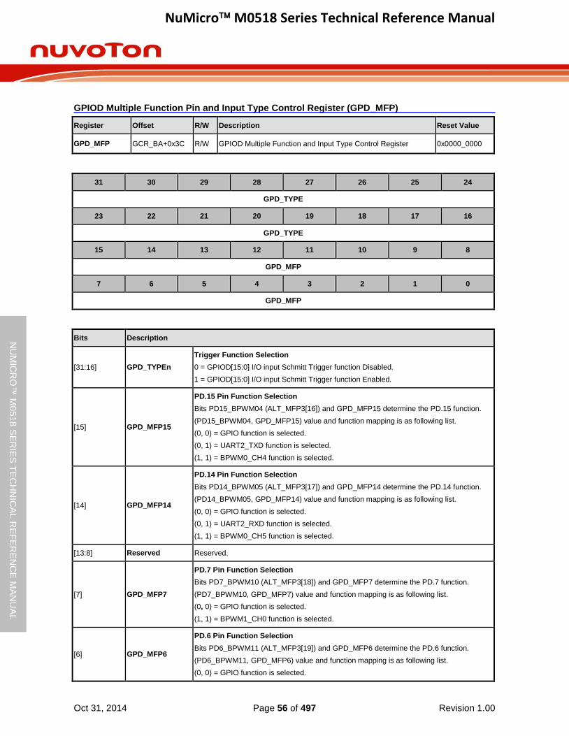
NuMicro M0518 Series Technical Reference Manual
Oct 31, 2014 Page 56 of 497 Revision 1.00
NU
MIC
RO
™ M
0518
SE
RIE
S T
EC
HN
ICA
L R
EF
ER
EN
CE
MA
NU
AL
GPIOD Multiple Function Pin and Input Type Control Register (GPD_MFP)
Register Offset R/W Description Reset Value
GPD_MFP GCR_BA+0x3C R/W GPIOD Multiple Function and Input Type Control Register 0x0000_0000
31 30 29 28 27 26 25 24
GPD_TYPE
23 22 21 20 19 18 17 16
GPD_TYPE
15 14 13 12 11 10 9 8
GPD_MFP
7 6 5 4 3 2 1 0
GPD_MFP
Bits Description
[31:16] GPD_TYPEn
Trigger Function Selection
0 = GPIOD[15:0] I/O input Schmitt Trigger function Disabled.
1 = GPIOD[15:0] I/O input Schmitt Trigger function Enabled.
[15] GPD_MFP15
PD.15 Pin Function Selection
Bits PD15_BPWM04 (ALT_MFP3[16]) and GPD_MFP15 determine the PD.15 function.
(PD15_BPWM04, GPD_MFP15) value and function mapping is as following list.
(0, 0) = GPIO function is selected.
(0, 1) = UART2_TXD function is selected.
(1, 1) = BPWM0_CH4 function is selected.
[14] GPD_MFP14
PD.14 Pin Function Selection
Bits PD14_BPWM05 (ALT_MFP3[17]) and GPD_MFP14 determine the PD.14 function.
(PD14_BPWM05, GPD_MFP14) value and function mapping is as following list.
(0, 0) = GPIO function is selected.
(0, 1) = UART2_RXD function is selected.
(1, 1) = BPWM0_CH5 function is selected.
[13:8] Reserved Reserved.
[7] GPD_MFP7
PD.7 Pin Function Selection
Bits PD7_BPWM10 (ALT_MFP3[18]) and GPD_MFP7 determine the PD.7 function.
(PD7_BPWM10, GPD_MFP7) value and function mapping is as following list.
(0, 0) = GPIO function is selected.
(1, 1) = BPWM1_CH0 function is selected.
[6] GPD_MFP6
PD.6 Pin Function Selection
Bits PD6_BPWM11 (ALT_MFP3[19]) and GPD_MFP6 determine the PD.6 function.
(PD6_BPWM11, GPD_MFP6) value and function mapping is as following list.
(0, 0) = GPIO function is selected.
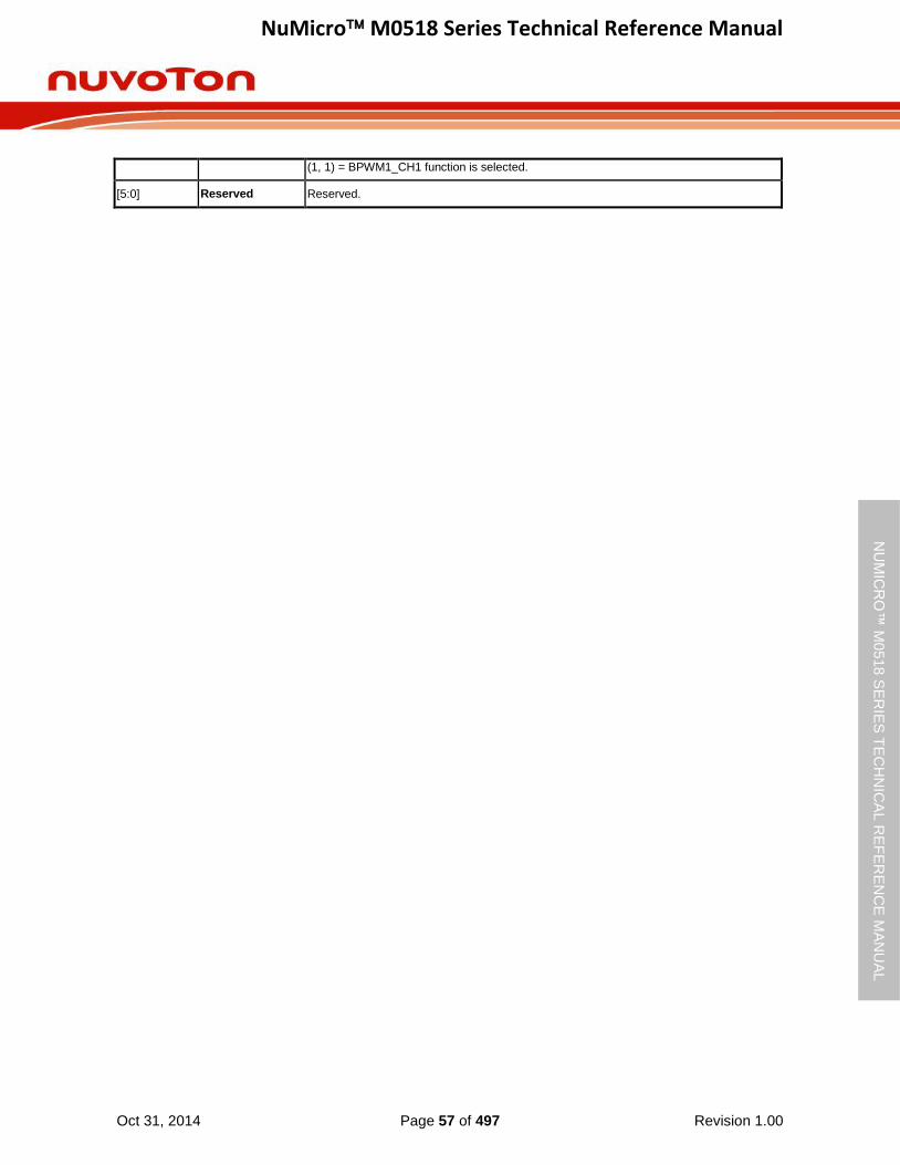
NuMicro M0518 Series Technical Reference Manual
Oct 31, 2014 Page 57 of 497 Revision 1.00
NU
MIC
RO
™ M
0518
SE
RIE
S T
EC
HN
ICA
L R
EF
ER
EN
CE
MA
NU
AL
(1, 1) = BPWM1_CH1 function is selected.
[5:0] Reserved Reserved.
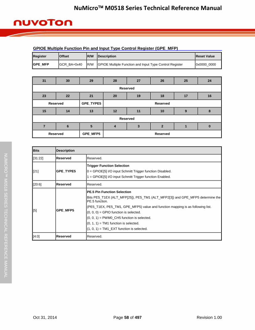
NuMicro M0518 Series Technical Reference Manual
Oct 31, 2014 Page 58 of 497 Revision 1.00
NU
MIC
RO
™ M
0518
SE
RIE
S T
EC
HN
ICA
L R
EF
ER
EN
CE
MA
NU
AL
GPIOE Multiple Function Pin and Input Type Control Register (GPE_MFP)
Register Offset R/W Description Reset Value
GPE_MFP GCR_BA+0x40 R/W GPIOE Multiple Function and Input Type Control Register 0x0000_0000
31 30 29 28 27 26 25 24
Reserved
23 22 21 20 19 18 17 16
Reserved GPE_TYPE5 Reserved
15 14 13 12 11 10 9 8
Reserved
7 6 5 4 3 2 1 0
Reserved GPE_MFP5 Reserved
Bits Description
[31:22] Reserved Reserved.
[21] GPE_TYPE5
Trigger Function Selection
0 = GPIOE[5] I/O input Schmitt Trigger function Disabled.
1 = GPIOE[5] I/O input Schmitt Trigger function Enabled.
[20:6] Reserved Reserved.
[5] GPE_MFP5
PE.5 Pin Function Selection
Bits PE5_T1EX (ALT_MFP[25]), PE5_TM1 (ALT_MFP2[3]) and GPE_MFP5 determine the PE.5 function.
(PE5_T1EX, PE5_TM1, GPE_MFP5) value and function mapping is as following list.
(0, 0, 0) = GPIO function is selected.
(0, 0, 1) = PWM0_CH5 function is selected.
(0, 1, 1) = TM1 function is selected.
(1, 0, 1) = TM1_EXT function is selected.
[4:0] Reserved Reserved.
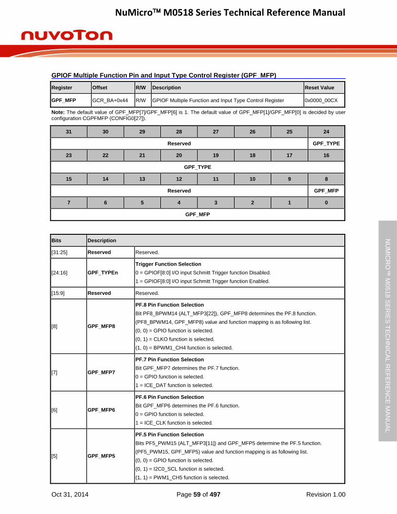
NuMicro M0518 Series Technical Reference Manual
Oct 31, 2014 Page 59 of 497 Revision 1.00
NU
MIC
RO
™ M
0518
SE
RIE
S T
EC
HN
ICA
L R
EF
ER
EN
CE
MA
NU
AL
GPIOF Multiple Function Pin and Input Type Control Register (GPF_MFP)
Register Offset R/W Description Reset Value
GPF_MFP GCR_BA+0x44 R/W GPIOF Multiple Function and Input Type Control Register 0x0000_00CX
Note: The default value of GPF_MFP[7]/GPF_MFP[6] is 1. The default value of GPF_MFP[1]/GPF_MFP[0] is decided by user configuration CGPFMFP (CONFIG0[27]).
31 30 29 28 27 26 25 24
Reserved GPF_TYPE
23 22 21 20 19 18 17 16
GPF_TYPE
15 14 13 12 11 10 9 8
Reserved GPF_MFP
7 6 5 4 3 2 1 0
GPF_MFP
Bits Description
[31:25] Reserved Reserved.
[24:16] GPF_TYPEn
Trigger Function Selection
0 = GPIOF[8:0] I/O input Schmitt Trigger function Disabled.
1 = GPIOF[8:0] I/O input Schmitt Trigger function Enabled.
[15:9] Reserved Reserved.
[8] GPF_MFP8
PF.8 Pin Function Selection
Bit PF8_BPWM14 (ALT_MFP3[22]), GPF_MFP8 determines the PF.8 function.
(PF8_BPWM14, GPF_MFP8) value and function mapping is as following list.
(0, 0) = GPIO function is selected.
(0, 1) = CLKO function is selected.
(1, 0) = BPWM1_CH4 function is selected.
[7] GPF_MFP7
PF.7 Pin Function Selection
Bit GPF_MFP7 determines the PF.7 function.
0 = GPIO function is selected.
1 = ICE_DAT function is selected.
[6] GPF_MFP6
PF.6 Pin Function Selection
Bit GPF_MFP6 determines the PF.6 function.
0 = GPIO function is selected.
1 = ICE_CLK function is selected.
[5] GPF_MFP5
PF.5 Pin Function Selection
Bits PF5_PWM15 (ALT_MFP3[11]) and GPF_MFP5 determine the PF.5 function.
(PF5_PWM15, GPF_MFP5) value and function mapping is as following list.
(0, 0) = GPIO function is selected.
(0, 1) = I2C0_SCL function is selected.
(1, 1) = PWM1_CH5 function is selected.
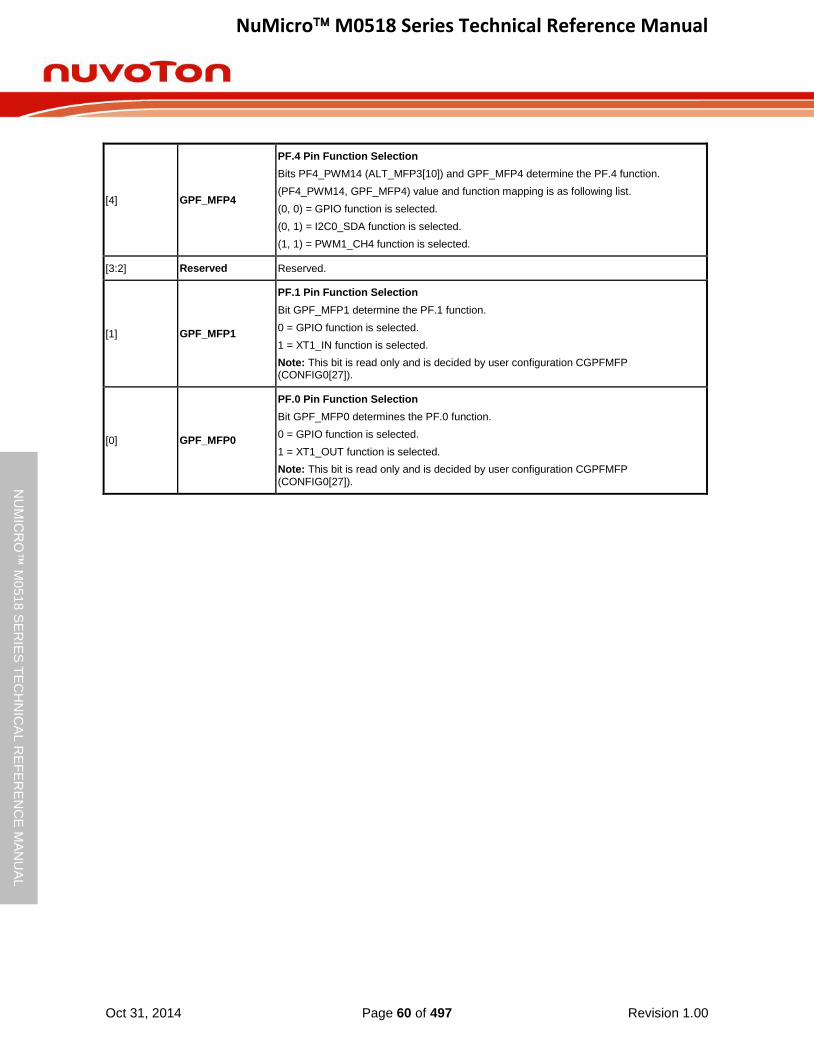
NuMicro M0518 Series Technical Reference Manual
Oct 31, 2014 Page 60 of 497 Revision 1.00
NU
MIC
RO
™ M
0518
SE
RIE
S T
EC
HN
ICA
L R
EF
ER
EN
CE
MA
NU
AL
[4] GPF_MFP4
PF.4 Pin Function Selection
Bits PF4_PWM14 (ALT_MFP3[10]) and GPF_MFP4 determine the PF.4 function.
(PF4_PWM14, GPF_MFP4) value and function mapping is as following list.
(0, 0) = GPIO function is selected.
(0, 1) = I2C0_SDA function is selected.
(1, 1) = PWM1_CH4 function is selected.
[3:2] Reserved Reserved.
[1] GPF_MFP1
PF.1 Pin Function Selection
Bit GPF_MFP1 determine the PF.1 function.
0 = GPIO function is selected.
1 = XT1_IN function is selected.
Note: This bit is read only and is decided by user configuration CGPFMFP (CONFIG0[27]).
[0] GPF_MFP0
PF.0 Pin Function Selection
Bit GPF_MFP0 determines the PF.0 function.
0 = GPIO function is selected.
1 = XT1_OUT function is selected.
Note: This bit is read only and is decided by user configuration CGPFMFP (CONFIG0[27]).
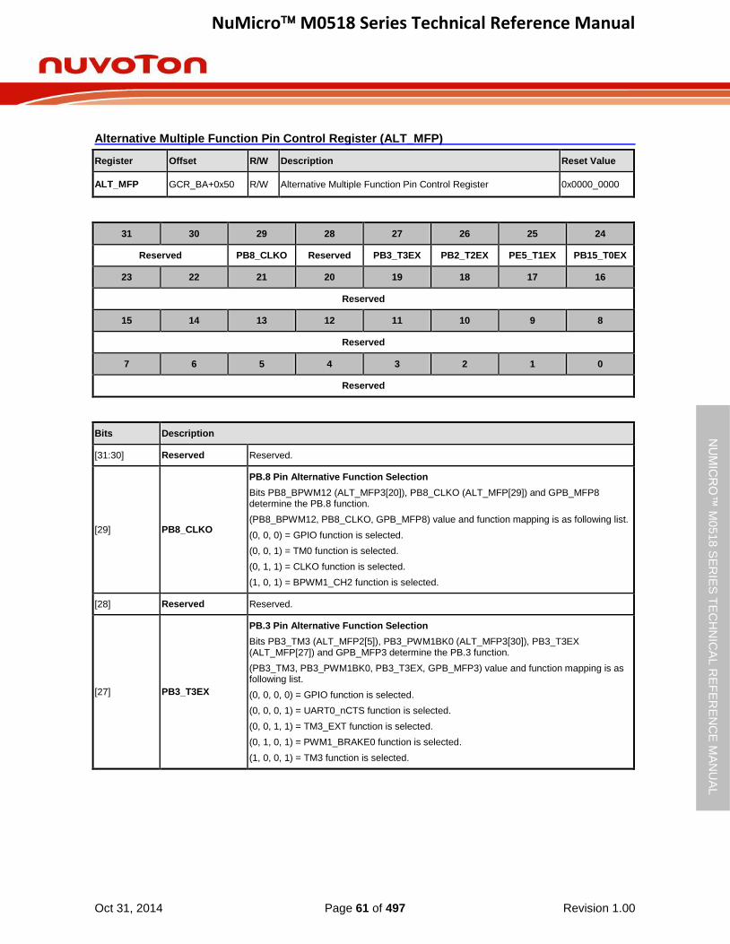
NuMicro M0518 Series Technical Reference Manual
Oct 31, 2014 Page 61 of 497 Revision 1.00
NU
MIC
RO
™ M
0518
SE
RIE
S T
EC
HN
ICA
L R
EF
ER
EN
CE
MA
NU
AL
Alternative Multiple Function Pin Control Register (ALT_MFP)
Register Offset R/W Description Reset Value
ALT_MFP GCR_BA+0x50 R/W Alternative Multiple Function Pin Control Register 0x0000_0000
31 30 29 28 27 26 25 24
Reserved PB8_CLKO Reserved PB3_T3EX PB2_T2EX PE5_T1EX PB15_T0EX
23 22 21 20 19 18 17 16
Reserved
15 14 13 12 11 10 9 8
Reserved
7 6 5 4 3 2 1 0
Reserved
Bits Description
[31:30] Reserved Reserved.
[29] PB8_CLKO
PB.8 Pin Alternative Function Selection
Bits PB8_BPWM12 (ALT_MFP3[20]), PB8_CLKO (ALT_MFP[29]) and GPB_MFP8 determine the PB.8 function.
(PB8_BPWM12, PB8_CLKO, GPB_MFP8) value and function mapping is as following list.
(0, 0, 0) = GPIO function is selected.
(0, 0, 1) = TM0 function is selected.
(0, 1, 1) = CLKO function is selected.
(1, 0, 1) = BPWM1_CH2 function is selected.
[28] Reserved Reserved.
[27] PB3_T3EX
PB.3 Pin Alternative Function Selection
Bits PB3_TM3 (ALT_MFP2[5]), PB3_PWM1BK0 (ALT_MFP3[30]), PB3_T3EX (ALT_MFP[27]) and GPB_MFP3 determine the PB.3 function.
(PB3_TM3, PB3_PWM1BK0, PB3_T3EX, GPB_MFP3) value and function mapping is as following list.
(0, 0, 0, 0) = GPIO function is selected.
(0, 0, 0, 1) = UART0_nCTS function is selected.
(0, 0, 1, 1) = TM3_EXT function is selected.
(0, 1, 0, 1) = PWM1_BRAKE0 function is selected.
(1, 0, 0, 1) = TM3 function is selected.

NuMicro M0518 Series Technical Reference Manual
Oct 31, 2014 Page 62 of 497 Revision 1.00
NU
MIC
RO
™ M
0518
SE
RIE
S T
EC
HN
ICA
L R
EF
ER
EN
CE
MA
NU
AL
[26] PB2_T2EX
PB.2 Pin Alternative Function Selection
Bits PB2_TM2 (ALT_MFP2[4]), PB2_PWM1BK1 (ALT_MFP3[31]), PB2_T2EX (ALT_MFP[26]) and GPB_MFP2 determine the PB.2 function.
(PB2_TM2, PB2_PWM1BK1, PB2_T2EX, GPB_MFP2) value and function mapping is as following list.
(0, 0, 0, 0) = GPIO function is selected.
(0, 0, 0, 1) = UART0_nRTS function is selected.
(0, 0, 1, 1) = TM2_EXT function is selected.
(0, 1, 0, 1) = PWM1_BRAKE1 function is selected.
(1, 0, 0, 1) = TM2 function is selected.
[25] PE5_T1EX
PE.5 Pin Alternative Function Selection
Bits PE5_T1EX (ALT_MFP[25]), PE5_TM1 (ALT_MFP2[3]) and GPE_MFP5 determine the PE.5 function.
(PE5_T1EX, PE5_TM1, GPE_MFP5) value and function mapping is as following list.
(0, 0, 0) = GPIO function is selected.
(0, 0, 1) = PWM0_CH5 function is selected.
(0, 1, 1) = TM1 function is selected.
(1, 0, 1) = TM1_EXT function is selected.
[24] PB15_T0EX
PB.15 Pin Alternative Function Selection
Bits PB15_BPWM15 (ALT_MFP3[23]), PB15_T0EX (ALT_MFP[24]), PB15_TM0 (ALT_MFP2[2]) and GPB_MFP15 determine the PB.15 function.
(PB15_BPWM15, PB15_T0EX, PB15_TM0, GPB_MFP15) value and function mapping is as following list.
(0, 0, 0, 0) = GPIO function is selected.
(0, 0, 0, 1) = INT1 function is selected.
(0, 0, 1, 1) = TM0 function is selected.
(0, 1, 0, 1) = TM0_EXT function is selected.
(1, 0, 1, 1) = BPWM1_CH5 function is selected.
[23:0] Reserved Reserved.
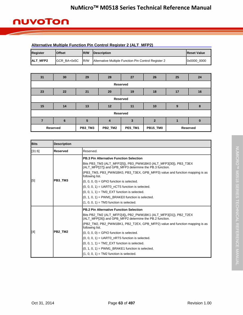
NuMicro M0518 Series Technical Reference Manual
Oct 31, 2014 Page 63 of 497 Revision 1.00
NU
MIC
RO
™ M
0518
SE
RIE
S T
EC
HN
ICA
L R
EF
ER
EN
CE
MA
NU
AL
Alternative Multiple Function Pin Control Register 2 (ALT_MFP2)
Register Offset R/W Description Reset Value
ALT_MFP2 GCR_BA+0x5C R/W Alternative Multiple Function Pin Control Register 2 0x0000_0000
31 30 29 28 27 26 25 24
Reserved
23 22 21 20 19 18 17 16
Reserved
15 14 13 12 11 10 9 8
Reserved
7 6 5 4 3 2 1 0
Reserved PB3_TM3 PB2_TM2 PE5_TM1 PB15_TM0 Reserved
Bits Description
[31:6] Reserved Reserved.
[5] PB3_TM3
PB.3 Pin Alternative Function Selection
Bits PB3_TM3 (ALT_MFP2[5]), PB3_PWM1BK0 (ALT_MFP3[30]), PB3_T3EX (ALT_MFP[27]) and GPB_MFP3 determine the PB.3 function.
(PB3_TM3, PB3_PWM1BK0, PB3_T3EX, GPB_MFP3) value and function mapping is as following list.
(0, 0, 0, 0) = GPIO function is selected.
(0, 0, 0, 1) = UART0_nCTS function is selected.
(0, 0, 1, 1) = TM3_EXT function is selected.
(0, 1, 0, 1) = PWM1_BRAKE0 function is selected.
(1, 0, 0, 1) = TM3 function is selected.
[4] PB2_TM2
PB.2 Pin Alternative Function Selection
Bits PB2_TM2 (ALT_MFP2[4]), PB2_PWM1BK1 (ALT_MFP3[31]), PB2_T2EX (ALT_MFP[26]) and GPB_MFP2 determine the PB.2 function.
(PB2_TM2, PB2_PWM1BK1, PB2_T2EX, GPB_MFP2) value and function mapping is as following list.
(0, 0, 0, 0) = GPIO function is selected.
(0, 0, 0, 1) = UART0_nRTS function is selected.
(0, 0, 1, 1) = TM2_EXT function is selected.
(0, 1, 0, 1) = PWM1_BRAKE1 function is selected.
(1, 0, 0, 1) = TM2 function is selected.
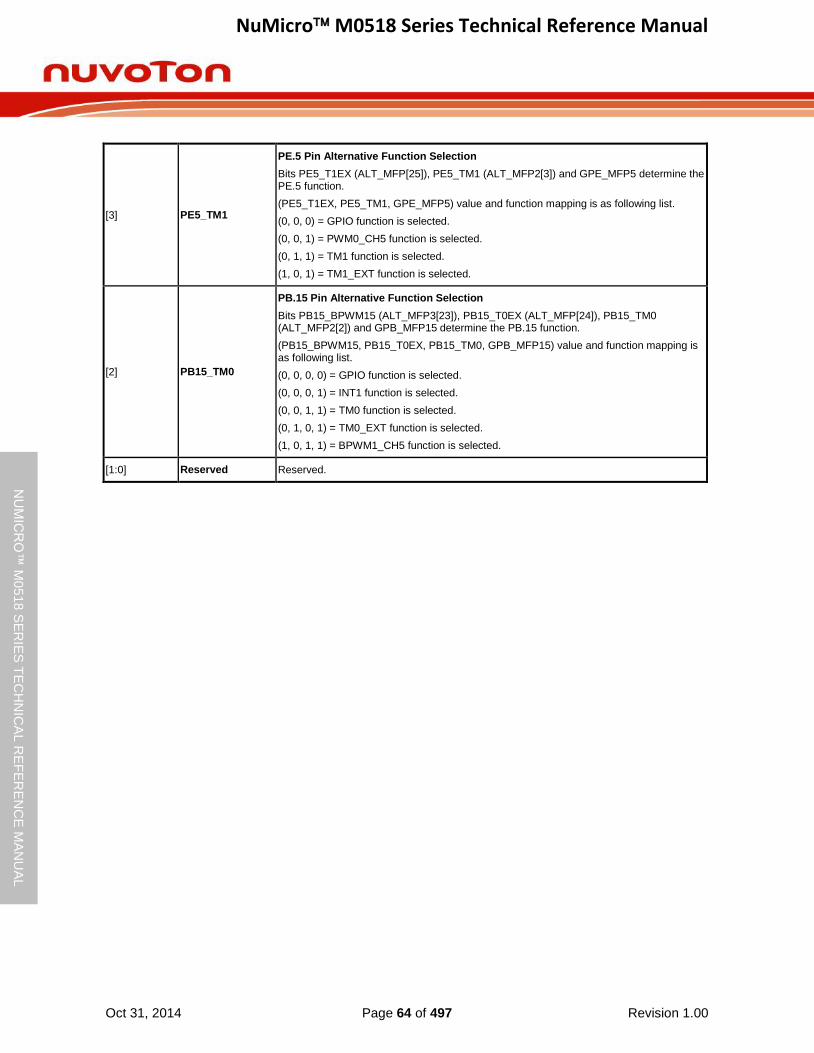
NuMicro M0518 Series Technical Reference Manual
Oct 31, 2014 Page 64 of 497 Revision 1.00
NU
MIC
RO
™ M
0518
SE
RIE
S T
EC
HN
ICA
L R
EF
ER
EN
CE
MA
NU
AL
[3] PE5_TM1
PE.5 Pin Alternative Function Selection
Bits PE5_T1EX (ALT_MFP[25]), PE5_TM1 (ALT_MFP2[3]) and GPE_MFP5 determine the PE.5 function.
(PE5_T1EX, PE5_TM1, GPE_MFP5) value and function mapping is as following list.
(0, 0, 0) = GPIO function is selected.
(0, 0, 1) = PWM0_CH5 function is selected.
(0, 1, 1) = TM1 function is selected.
(1, 0, 1) = TM1_EXT function is selected.
[2] PB15_TM0
PB.15 Pin Alternative Function Selection
Bits PB15_BPWM15 (ALT_MFP3[23]), PB15_T0EX (ALT_MFP[24]), PB15_TM0 (ALT_MFP2[2]) and GPB_MFP15 determine the PB.15 function.
(PB15_BPWM15, PB15_T0EX, PB15_TM0, GPB_MFP15) value and function mapping is as following list.
(0, 0, 0, 0) = GPIO function is selected.
(0, 0, 0, 1) = INT1 function is selected.
(0, 0, 1, 1) = TM0 function is selected.
(0, 1, 0, 1) = TM0_EXT function is selected.
(1, 0, 1, 1) = BPWM1_CH5 function is selected.
[1:0] Reserved Reserved.
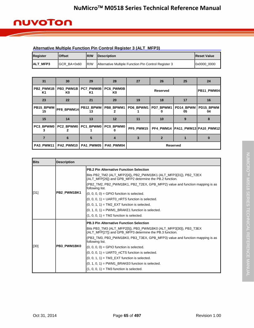
NuMicro M0518 Series Technical Reference Manual
Oct 31, 2014 Page 65 of 497 Revision 1.00
NU
MIC
RO
™ M
0518
SE
RIE
S T
EC
HN
ICA
L R
EF
ER
EN
CE
MA
NU
AL
Alternative Multiple Function Pin Control Register 3 (ALT_MFP3)
Register Offset R/W Description Reset Value
ALT_MFP3 GCR_BA+0x60 R/W Alternative Multiple Function Pin Control Register 3 0x0000_0000
31 30 29 28 27 26 25 24
PB2_PWM1BK1
PB3_PWM1BK0
PC7_PWM0BK1
PC6_PWM0BK0
Reserved PB11_PWM04
23 22 21 20 19 18 17 16
PB15_BPWM15
PF8_BPWM14 PB12_BPWM
13 PB8_BPWM1
2 PD6_BPWM1
1 PD7_BPWM1
0 PD14_BPWM
05 PD15_BPWM
04
15 14 13 12 11 10 9 8
PC3_BPWM03
PC2_BPWM02
PC1_BPWM01
PC0_BPWM00
PF5_PWM15 PF4_PWM14 PA11_PWM13 PA10_PWM12
7 6 5 4 3 2 1 0
PA3_PWM11 PA2_PWM10 PA1_PWM05 PA0_PWM04 Reserved
Bits Description
[31] PB2_PWM1BK1
PB.2 Pin Alternative Function Selection
Bits PB2_TM2 (ALT_MFP2[4]), PB2_PWM1BK1 (ALT_MFP3[31]), PB2_T2EX (ALT_MFP[26]) and GPB_MFP2 determine the PB.2 function.
(PB2_TM2, PB2_PWM1BK1, PB2_T2EX, GPB_MFP2) value and function mapping is as following list.
(0, 0, 0, 0) = GPIO function is selected.
(0, 0, 0, 1) = UART0_nRTS function is selected.
(0, 0, 1, 1) = TM2_EXT function is selected.
(0, 1, 0, 1) = PWM1_BRAKE1 function is selected.
(1, 0, 0, 1) = TM2 function is selected.
[30] PB3_PWM1BK0
PB.3 Pin Alternative Function Selection
Bits PB3_TM3 (ALT_MFP2[5]), PB3_PWM1BK0 (ALT_MFP3[30]), PB3_T3EX (ALT_MFP[27]) and GPB_MFP3 determine the PB.3 function.
(PB3_TM3, PB3_PWM1BK0, PB3_T3EX, GPB_MFP3) value and function mapping is as following list.
(0, 0, 0, 0) = GPIO function is selected.
(0, 0, 0, 1) = UART0_nCTS function is selected.
(0, 0, 1, 1) = TM3_EXT function is selected.
(0, 1, 0, 1) = PWM1_BRAKE0 function is selected.
(1, 0, 0, 1) = TM3 function is selected.

NuMicro M0518 Series Technical Reference Manual
Oct 31, 2014 Page 66 of 497 Revision 1.00
NU
MIC
RO
™ M
0518
SE
RIE
S T
EC
HN
ICA
L R
EF
ER
EN
CE
MA
NU
AL
[29] PC7_PWM0BK1
PC.7 Pin Alternative Function Selection
Bits PC7_PWM0BK1 (ALT_MFP3[29]), PC7_I2C0SCL (ALT_MFP4[11]) and GPC_MFP7 determine the PC.7 function.
(PC7_PWM0BK1, PC7_I2C0SCL, GPC_MFP7) value and function mapping is as following list.
(0, 0, 0) = GPIO function is selected.
(0, 0, 1) = UART4_RXD function is selected.
(0, 1, 1) = I2C0_SCL function is selected.
(1, 0, 1) = PWM0_BRAKE1 function is selected.
[28] PC6_PWM0BK0
PC.6 Pin Alternative Function Selection
Bits PC6_PWM0BK0 (ALT_MFP3[28]), PC6_I2C0SDA (ALT_MFP4[10]) and GPC_MFP6 determine the PC.6 function.
(PC6_PWM0BK0, PC6_I2C0SDA, GPB_MFP6) value and function mapping is as following list.
(0, 0, 0) = GPIO function is selected.
(0, 0, 1) = UART4_TXD function is selected.
(0, 1, 1) = I2C0_SDA function is selected.
(1, 0, 1) = PWM0_BRAKE0 function is selected.
[27:25] Reserved Reserved.
[24] PB11_PWM04
PB.11 Pin Alternative Function Selection
Bits PB11_PWM04 (ALT_MFP3[24]) and GPB_MFP11 determine the PB.11 function.
(PB11_PWM04, GPB_MFP11) value and function mapping is as following list.
(0, 0) = GPIO function is selected.
(0, 1) = TM3 function is selected.
(1, 1) = PWM0_CH4 function is selected.
[23] PB15_BPWM15
PB.15 Pin Function Selection
Bits PB15_BPWM15 (ALT_MFP3[23]), PB15_T0EX (ALT_MFP[24]), PB15_TM0 (ALT_MFP2[2]) and GPB_MFP15 determine the PB.15 function.
(PB15_BPWM15, PB15_T0EX, PB15_TM0, GPB_MFP15) value and function mapping is as following list.
(0, 0, 0, 0) = GPIO function is selected.
(0, 0, 0, 1) = INT1 function is selected.
(0, 0, 1, 1) = TM0 function is selected.
(0, 1, 0, 1) = TM0_EXT function is selected.
(1, 0, 1, 1) = BPWM1_CH5 function is selected.
[22] PF8_BPWM14
PF.8 Pin Function Selection
Bit PF8_BPWM14 (ALT_MFP3[22]), GPF_MFP8 determines the PF.8 function.
(PF8_BPWM14, GPF_MFP8) value and function mapping is as following list.
(0, 0) = GPIO function is selected.
(0, 1) = CLKO function is selected.
(1, 0) = BPWM1_CH4 function is selected.
[21] PB12_BPWM13
PB.12 Pin Alternative Function Selection
Bits PB12_BPWM13 (ALT_MFP3[21]) and GPB_MFP12 determine the PB.12 function.
(PB12_BPWM13, GPB_MFP12) value and function mapping is as following list.
(0, 0) = GPIO function is selected.
(0, 1) = CLKO function is selected.
(1, 1) = BPWM1_CH3 function is selected.
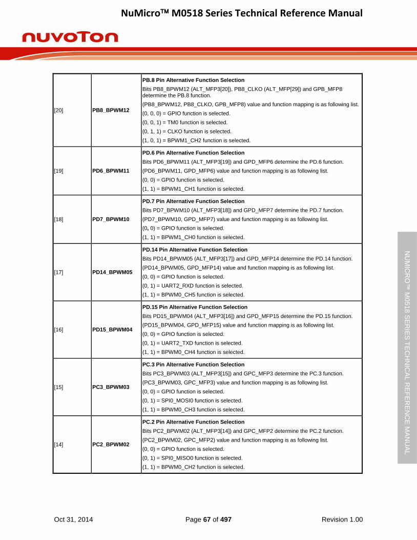
NuMicro M0518 Series Technical Reference Manual
Oct 31, 2014 Page 67 of 497 Revision 1.00
NU
MIC
RO
™ M
0518
SE
RIE
S T
EC
HN
ICA
L R
EF
ER
EN
CE
MA
NU
AL
[20] PB8_BPWM12
PB.8 Pin Alternative Function Selection
Bits PB8_BPWM12 (ALT_MFP3[20]), PB8_CLKO (ALT_MFP[29]) and GPB_MFP8 determine the PB.8 function.
(PB8_BPWM12, PB8_CLKO, GPB_MFP8) value and function mapping is as following list.
(0, 0, 0) = GPIO function is selected.
(0, 0, 1) = TM0 function is selected.
(0, 1, 1) = CLKO function is selected.
(1, 0, 1) = BPWM1_CH2 function is selected.
[19] PD6_BPWM11
PD.6 Pin Alternative Function Selection
Bits PD6_BPWM11 (ALT_MFP3[19]) and GPD_MFP6 determine the PD.6 function.
(PD6_BPWM11, GPD_MFP6) value and function mapping is as following list.
(0, 0) = GPIO function is selected.
(1, 1) = BPWM1_CH1 function is selected.
[18] PD7_BPWM10
PD.7 Pin Alternative Function Selection
Bits PD7_BPWM10 (ALT_MFP3[18]) and GPD_MFP7 determine the PD.7 function.
(PD7_BPWM10, GPD_MFP7) value and function mapping is as following list.
(0, 0) = GPIO function is selected.
(1, 1) = BPWM1_CH0 function is selected.
[17] PD14_BPWM05
PD.14 Pin Alternative Function Selection
Bits PD14_BPWM05 (ALT_MFP3[17]) and GPD_MFP14 determine the PD.14 function.
(PD14_BPWM05, GPD_MFP14) value and function mapping is as following list.
(0, 0) = GPIO function is selected.
(0, 1) = UART2_RXD function is selected.
(1, 1) = BPWM0_CH5 function is selected.
[16] PD15_BPWM04
PD.15 Pin Alternative Function Selection
Bits PD15_BPWM04 (ALT_MFP3[16]) and GPD_MFP15 determine the PD.15 function.
(PD15_BPWM04, GPD_MFP15) value and function mapping is as following list.
(0, 0) = GPIO function is selected.
(0, 1) = UART2_TXD function is selected.
(1, 1) = BPWM0_CH4 function is selected.
[15] PC3_BPWM03
PC.3 Pin Alternative Function Selection
Bits PC3_BPWM03 (ALT_MFP3[15]) and GPC_MFP3 determine the PC.3 function.
(PC3_BPWM03, GPC_MFP3) value and function mapping is as following list.
(0, 0) = GPIO function is selected.
(0, 1) = SPI0_MOSI0 function is selected.
(1, 1) = BPWM0_CH3 function is selected.
[14] PC2_BPWM02
PC.2 Pin Alternative Function Selection
Bits PC2_BPWM02 (ALT_MFP3[14]) and GPC_MFP2 determine the PC.2 function.
(PC2_BPWM02, GPC_MFP2) value and function mapping is as following list.
(0, 0) = GPIO function is selected.
(0, 1) = SPI0_MISO0 function is selected.
(1, 1) = BPWM0_CH2 function is selected.
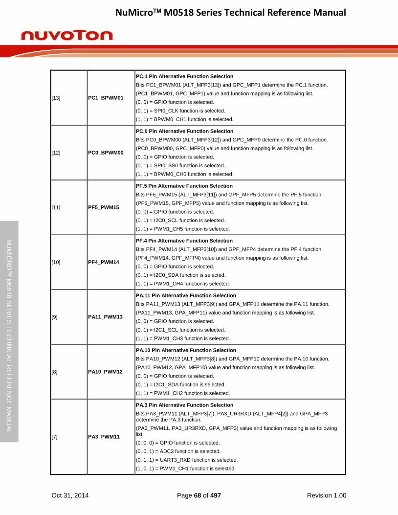
NuMicro M0518 Series Technical Reference Manual
Oct 31, 2014 Page 68 of 497 Revision 1.00
NU
MIC
RO
™ M
0518
SE
RIE
S T
EC
HN
ICA
L R
EF
ER
EN
CE
MA
NU
AL
[13] PC1_BPWM01
PC.1 Pin Alternative Function Selection
Bits PC1_BPWM01 (ALT_MFP3[13]) and GPC_MFP1 determine the PC.1 function.
(PC1_BPWM01, GPC_MFP1) value and function mapping is as following list.
(0, 0) = GPIO function is selected.
(0, 1) = SPI0_CLK function is selected.
(1, 1) = BPWM0_CH1 function is selected.
[12] PC0_BPWM00
PC.0 Pin Alternative Function Selection
Bits PC0_BPWM00 (ALT_MFP3[12]) and GPC_MFP0 determine the PC.0 function.
(PC0_BPWM00, GPC_MFP0) value and function mapping is as following list.
(0, 0) = GPIO function is selected.
(0, 1) = SPI0_SS0 function is selected.
(1, 1) = BPWM0_CH0 function is selected.
[11] PF5_PWM15
PF.5 Pin Alternative Function Selection
Bits PF5_PWM15 (ALT_MFP3[11]) and GPF_MFP5 determine the PF.5 function.
(PF5_PWM15, GPF_MFP5) value and function mapping is as following list.
(0, 0) = GPIO function is selected.
(0, 1) = I2C0_SCL function is selected.
(1, 1) = PWM1_CH5 function is selected.
[10] PF4_PWM14
PF.4 Pin Alternative Function Selection
Bits PF4_PWM14 (ALT_MFP3[10]) and GPF_MFP4 determine the PF.4 function.
(PF4_PWM14, GPF_MFP4) value and function mapping is as following list.
(0, 0) = GPIO function is selected.
(0, 1) = I2C0_SDA function is selected.
(1, 1) = PWM1_CH4 function is selected.
[9] PA11_PWM13
PA.11 Pin Alternative Function Selection
Bits PA11_PWM13 (ALT_MFP3[9]) and GPA_MFP11 determine the PA.11 function.
(PA11_PWM13, GPA_MFP11) value and function mapping is as following list.
(0, 0) = GPIO function is selected.
(0, 1) = I2C1_SCL function is selected.
(1, 1) = PWM1_CH3 function is selected.
[8] PA10_PWM12
PA.10 Pin Alternative Function Selection
Bits PA10_PWM12 (ALT_MFP3[8]) and GPA_MFP10 determine the PA.10 function.
(PA10_PWM12, GPA_MFP10) value and function mapping is as following list.
(0, 0) = GPIO function is selected.
(0, 1) = I2C1_SDA function is selected.
(1, 1) = PWM1_CH2 function is selected.
[7] PA3_PWM11
PA.3 Pin Alternative Function Selection
Bits PA3_PWM11 (ALT_MFP3[7]), PA3_UR3RXD (ALT_MFP4[2]) and GPA_MFP3 determine the PA.3 function.
(PA3_PWM11, PA3_UR3RXD, GPA_MFP3) value and function mapping is as following list.
(0, 0, 0) = GPIO function is selected.
(0, 0, 1) = ADC3 function is selected.
(0, 1, 1) = UART3_RXD function is selected.
(1, 0, 1) = PWM1_CH1 function is selected.

NuMicro M0518 Series Technical Reference Manual
Oct 31, 2014 Page 69 of 497 Revision 1.00
NU
MIC
RO
™ M
0518
SE
RIE
S T
EC
HN
ICA
L R
EF
ER
EN
CE
MA
NU
AL
[6] PA2_PWM10
PA.2 Pin Alternative Function Selection
Bits PA2_PWM10 (ALT_MFP3[6]), PA2_UR3TXD (ALT_MFP4[3]) and GPA_MFP2 determine the PA.2 function.
(PA2_PWM10, PA2_UR3TXD, GPA_MFP2) value and function mapping is as following list.
(0, 0, 0) = GPIO function is selected.
(0, 0, 1) = ADC2 function is selected.
(0, 1, 1) = UART3_TXD function is selected.
(1, 0, 1) = PWM1_CH0 function is selected.
[5] PA1_PWM05
PA.1 Pin Alternative Function Selection
Bits PA1_PWM05 (ALT_MFP3[5]), PA1_UR5RXD (ALT_MFP4[6]), PA1_I2C1SDA (ALT_MFP4[13]) and GPA_MFP1 determine the PA.1 function.
(PA1_PWM05, PA1_UR5RXD , PA1_I2C1SDA, GPA_MFP1) value and function mapping is as following list.
(0, 0, 0, 0) = GPIO function is selected.
(0, 0, 0, 1) = ADC1 function is selected.
(0, 0, 1, 1) = I2C1_SDA function is selected.
(0, 1, 0, 1) = UART5_RXD function is selected.
(1, 0, 0, 1) = PWM0_CH5 function is selected.
[4] PA0_PWM04
PA.0 Pin Alternative Function Selection
Bits PA0_PWM04 (ALT_MFP3[4]), PA0_UR5TXD (ALT_MFP4[7]), PA0_I2C1SCL (ALT_MFP4[12]) and GPA_MFP0 determine the PA.0 function.
(PA0_PWM04, PA0_UR5TXD, PA0_I2C1SCL, GPA_MFP0) value and function mapping is as following list.
(0, 0, 0, 0) = GPIO function is selected.
(0, 0, 0, 1) = ADC0 function is selected.
(0, 0, 1, 1) = I2C1_SCL function is selected.
(0, 1, 0, 1) = UART5_TXD function is selected.
(1, 0, 0, 1) = PWM0_CH4 function is selected.
[3:0] Reserved Reserved.
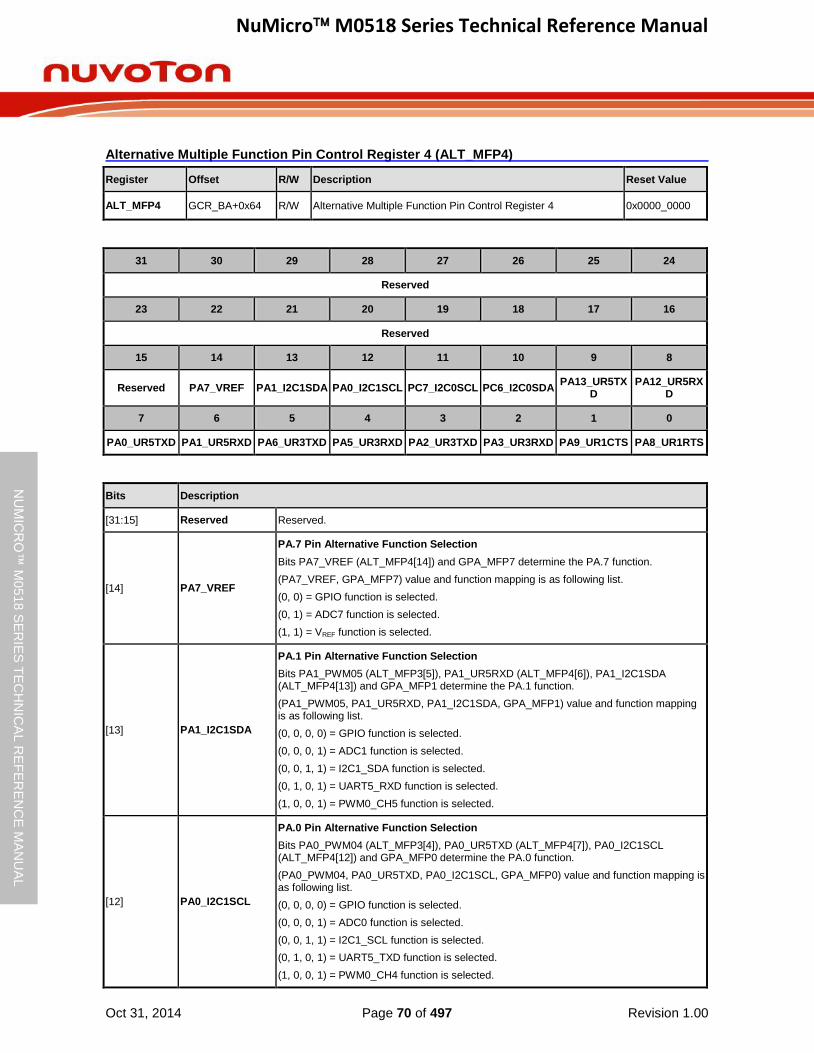
NuMicro M0518 Series Technical Reference Manual
Oct 31, 2014 Page 70 of 497 Revision 1.00
NU
MIC
RO
™ M
0518
SE
RIE
S T
EC
HN
ICA
L R
EF
ER
EN
CE
MA
NU
AL
Alternative Multiple Function Pin Control Register 4 (ALT_MFP4)
Register Offset R/W Description Reset Value
ALT_MFP4 GCR_BA+0x64 R/W Alternative Multiple Function Pin Control Register 4 0x0000_0000
31 30 29 28 27 26 25 24
Reserved
23 22 21 20 19 18 17 16
Reserved
15 14 13 12 11 10 9 8
Reserved PA7_VREF PA1_I2C1SDA PA0_I2C1SCL PC7_I2C0SCL PC6_I2C0SDA PA13_UR5TX
D PA12_UR5RX
D
7 6 5 4 3 2 1 0
PA0_UR5TXD PA1_UR5RXD PA6_UR3TXD PA5_UR3RXD PA2_UR3TXD PA3_UR3RXD PA9_UR1CTS PA8_UR1RTS
Bits Description
[31:15] Reserved Reserved.
[14] PA7_VREF
PA.7 Pin Alternative Function Selection
Bits PA7_VREF (ALT_MFP4[14]) and GPA_MFP7 determine the PA.7 function.
(PA7_VREF, GPA_MFP7) value and function mapping is as following list.
(0, 0) = GPIO function is selected.
(0, 1) = ADC7 function is selected.
(1, 1) = VREF function is selected.
[13] PA1_I2C1SDA
PA.1 Pin Alternative Function Selection
Bits PA1_PWM05 (ALT_MFP3[5]), PA1_UR5RXD (ALT_MFP4[6]), PA1_I2C1SDA (ALT_MFP4[13]) and GPA_MFP1 determine the PA.1 function.
(PA1_PWM05, PA1_UR5RXD, PA1_I2C1SDA, GPA_MFP1) value and function mapping is as following list.
(0, 0, 0, 0) = GPIO function is selected.
(0, 0, 0, 1) = ADC1 function is selected.
(0, 0, 1, 1) = I2C1_SDA function is selected.
(0, 1, 0, 1) = UART5_RXD function is selected.
(1, 0, 0, 1) = PWM0_CH5 function is selected.
[12] PA0_I2C1SCL
PA.0 Pin Alternative Function Selection
Bits PA0_PWM04 (ALT_MFP3[4]), PA0_UR5TXD (ALT_MFP4[7]), PA0_I2C1SCL (ALT_MFP4[12]) and GPA_MFP0 determine the PA.0 function.
(PA0_PWM04, PA0_UR5TXD, PA0_I2C1SCL, GPA_MFP0) value and function mapping is as following list.
(0, 0, 0, 0) = GPIO function is selected.
(0, 0, 0, 1) = ADC0 function is selected.
(0, 0, 1, 1) = I2C1_SCL function is selected.
(0, 1, 0, 1) = UART5_TXD function is selected.
(1, 0, 0, 1) = PWM0_CH4 function is selected.

NuMicro M0518 Series Technical Reference Manual
Oct 31, 2014 Page 71 of 497 Revision 1.00
NU
MIC
RO
™ M
0518
SE
RIE
S T
EC
HN
ICA
L R
EF
ER
EN
CE
MA
NU
AL
[11] PC7_I2C0SCL
PC.7 Pin Alternative Function Selection
Bits PC7_PWM0BK1 (ALT_MFP3[29]), PC7_I2C0SCL (ALT_MFP4[11]) and GPC_MFP7 determine the PC.7 function.
(PC7_PWM0BK1, PC7_I2C0SCL, GPC_MFP7) value and function mapping is as following list.
(0, 0, 0) = GPIO function is selected.
(0, 0, 1) = UART4_RXD function is selected.
(0, 1, 1) = I2C0_SCL function is selected.
(1, 0, 1) = PWM0_BRAKE1 function is selected.
[10] PC6_I2C0SDA
PC.6 Pin Alternative Function Selection
Bits PC6_PWM0BK0 (ALT_MFP3[28]), PC6_I2C0SDA (ALT_MFP4[10]) and GPC_MFP6 determine the PC.6 function.
(PC6_PWM0BK0, PC6_I2C0SDA, GPC_MFP6) value and function mapping is as following list.
(0, 0, 0) = GPIO function is selected.
(0, 0, 1) = UART4_TXD function is selected.
(0, 1, 1) = I2C0_SDA function is selected.
(1, 0, 1) = PWM0_BRAKE0 function is selected.
[9] PA13_UR5TXD
PA.13 Pin Alternative Function Selection
Bits PA13_UR5TXD (ALT_MFP4[9]) and GPA_MFP13 determine the PA.13 function.
(PA13_UR5TXD, GPA_MFP13) value and function mapping is as following list.
(0, 0) = GPIO function is selected.
(0, 1) = PWM0_CH1 function is selected.
(1, 1) = UART5_TXD function is selected.
[8] PA12_UR5RXD
PA.12 Pin Alternative Function Selection
Bits PA12_UR5RXD (ALT_MFP4[8]) and GPA_MFP12 determine the PA.12 function.
(PA12_UR5RXD, GPA_MFP12) value and function mapping is as following list.
(0, 0) = GPIO function is selected.
(0, 1) = PWM0_CH0 function is selected.
(1, 1) = UART5_RXD function is selected.
[7] PA0_UR5TXD
PA.0 Pin Alternative Function Selection
Bits PA0_PWM04 (ALT_MFP3[4]), PA0_UR5TXD (ALT_MFP4[7]), PA0_I2C1SCL (ALT_MFP4[12]) and GPA_MFP0 determine the PA.0 function.
(PA0_PWM04, PA0_UR5TXD, PA0_I2C1SCL, GPA_MFP0) value and function mapping is as following list.
(0, 0, 0, 0) = GPIO function is selected.
(0, 0, 0, 1) = ADC0 function is selected.
(0, 0, 1, 1) = I2C1_SCL function is selected.
(0, 1, 0, 1) = UART5_TXD function is selected.
(1, 0, 0, 1) = PWM0_CH4 function is selected.
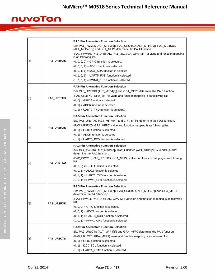
NuMicro M0518 Series Technical Reference Manual
Oct 31, 2014 Page 72 of 497 Revision 1.00
NU
MIC
RO
™ M
0518
SE
RIE
S T
EC
HN
ICA
L R
EF
ER
EN
CE
MA
NU
AL
[6] PA1_UR5RXD
PA.1 Pin Alternative Function Selection
Bits PA1_PWM05 (ALT_MFP3[5]), PA1_UR5RXD (ALT_MFP4[6]), PA1_I2C1SDA (ALT_MFP4[13]) and GPA_MFP1 determine the PA.1 function.
(PA1_PWM05, PA1_UR5RXD, PA1_I2C1SDA, GPA_MFP1) value and function mapping is as following list.
(0, 0, 0, 0) = GPIO function is selected.
(0, 0, 0, 1) = ADC1 function is selected.
(0, 0, 1, 1) = I2C1_SDA function is selected.
(0, 1, 0, 1) = UART5_RXD function is selected.
(1, 0, 0, 1) = PWM0_CH5 function is selected.
[5] PA6_UR3TXD
PA.6 Pin Alternative Function Selection
Bits PA6_UR3TXD (ALT_MFP4[5]) and GPA_MFP6 determine the PA.6 function.
(PA6_UR3TXD, GPA_MFP6) value and function mapping is as following list.
(0, 0) = GPIO function is selected.
(0, 1) = ADC6 function is selected.
(1, 1) = UART3_TXD function is selected.
[4] PA5_UR3RXD
PA.5 Pin Alternative Function Selection
Bits PA5_UR3RXD (ALT_MFP4[4]) and GPA_MFP5 determine the PA.5 function.
(PA5_UR3RXD, GPA_MFP5) value and function mapping is as following list.
(0, 0) = GPIO function is selected.
(0, 1) = ADC5 function is selected.
(1, 1) = UART3_RXD function is selected.
[3] PA2_UR3TXD
PA.2 Pin Alternative Function Selection
Bits PA2_PWM10 (ALT_MFP3[6]), PA2_UR3TXD (ALT_MFP4[3]) and GPA_MFP2 determine the PA.2 function.
(PA2_PWM10, PA2_UR3TXD, GPA_MFP2) value and function mapping is as following list.
(0, 0, 0) = GPIO function is selected.
(0, 0, 1) = ADC2 function is selected.
(0, 1, 1) = UART3_TXD function is selected.
(1, 0, 1) = PWM1_CH0 function is selected.
[2] PA3_UR3RXD
PA.3 Pin Alternative Function Selection
Bits PA3_PWM11 (ALT_MFP3[7]), PA3_UR3RXD (ALT_MFP4[2]) and GPA_MFP3 determine the PA.3 function.
(PA3_PWM11, PA3_UR3RXD, GPA_MFP3) value and function mapping is as following list.
(0, 0, 0) = GPIO function is selected.
(0, 0, 1) = ADC3 function is selected.
(0, 1, 1) = UART3_RXD function is selected.
(1, 0, 1) = PWM1_CH1 function is selected.
[1] PA9_UR1CTS
PA.9 Pin Alternative Function Selection
Bits PA9_UR1CTS (ALT_MFP4[1]) and GPA_MFP9 determine the PA.9 function.
(PA9_UR1CTS, GPA_MFP9) value and function mapping is as following list.
(0, 0) = GPIO function is selected.
(0, 1) = I2C0_SCL function is selected.
(1, 1) = UART1_nCTS function is selected.
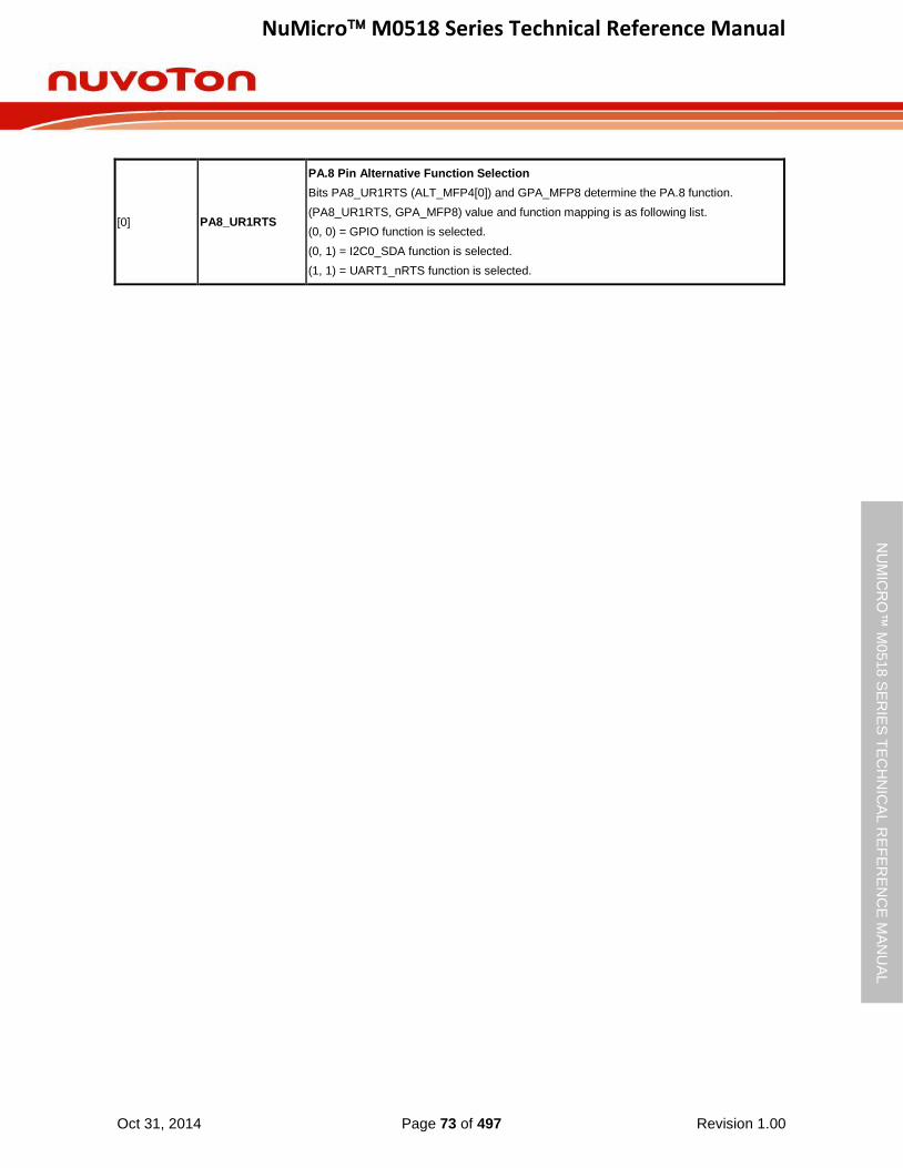
NuMicro M0518 Series Technical Reference Manual
Oct 31, 2014 Page 73 of 497 Revision 1.00
NU
MIC
RO
™ M
0518
SE
RIE
S T
EC
HN
ICA
L R
EF
ER
EN
CE
MA
NU
AL
[0] PA8_UR1RTS
PA.8 Pin Alternative Function Selection
Bits PA8_UR1RTS (ALT_MFP4[0]) and GPA_MFP8 determine the PA.8 function.
(PA8_UR1RTS, GPA_MFP8) value and function mapping is as following list.
(0, 0) = GPIO function is selected.
(0, 1) = I2C0_SDA function is selected.
(1, 1) = UART1_nRTS function is selected.
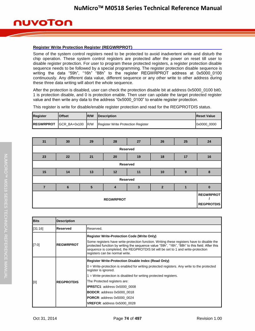
NuMicro M0518 Series Technical Reference Manual
Oct 31, 2014 Page 74 of 497 Revision 1.00
NU
MIC
RO
™ M
0518
SE
RIE
S T
EC
HN
ICA
L R
EF
ER
EN
CE
MA
NU
AL
Register Write Protection Register (REGWRPROT)
Some of the system control registers need to be protected to avoid inadvertent write and disturb the chip operation. These system control registers are protected after the power on reset till user to disable register protection. For user to program these protected registers, a register protection disable sequence needs to be followed by a special programming. The register protection disable sequence is writing the data “59h”, “16h” “88h” to the register REGWRPROT address at 0x5000_0100 continuously. Any different data value, different sequence or any other write to other address during these three data writing will abort the whole sequence.
After the protection is disabled, user can check the protection disable bit at address 0x5000_0100 bit0, 1 is protection disable, and 0 is protection enable. Then user can update the target protected register value and then write any data to the address “0x5000_0100” to enable register protection.
This register is write for disable/enable register protection and read for the REGPROTDIS status.
Register Offset R/W Description Reset Value
REGWRPROT GCR_BA+0x100 R/W Register Write Protection Register 0x0000_0000
31 30 29 28 27 26 25 24
Reserved
23 22 21 20 19 18 17 16
Reserved
15 14 13 12 11 10 9 8
Reserved
7 6 5 4 3 2 1 0
REGWRPROT
REGWRPROT /
REGPROTDIS
Bits Description
[31:16] Reserved Reserved.
[7:0] REGWRPROT
Register Write-Protection Code (Write Only)
Some registers have write-protection function. Writing these registers have to disable the protected function by writing the sequence value “59h”, “16h”, “88h” to this field. After this sequence is completed, the REGPROTDIS bit will be set to 1 and write-protection registers can be normal write.
[0] REGPROTDIS
Register Write-Protection Disable Index (Read Only)
0 = Write-protection is enabled for writing protected registers. Any write to the protected register is ignored.
1 = Write-protection is disabled for writing protected registers.
The Protected registers are:
IPRSTC1: address 0x5000_0008
BODCR: address 0x5000_0018
PORCR: address 0x5000_0024
VREFCR: address 0x5000_0028

NuMicro M0518 Series Technical Reference Manual
Oct 31, 2014 Page 75 of 497 Revision 1.00
NU
MIC
RO
™ M
0518
SE
RIE
S T
EC
HN
ICA
L R
EF
ER
EN
CE
MA
NU
AL
PWRCON: address 0x5000_0200 (bit[6] is not protected for power wake-up interrupt clear)
APBCLK bit[0]: address 0x5000_0208 (bit[0] is Watchdog Timer clock enable)
CLKSEL0: address 0x5000_0210 (for HCLK and CPU STCLK clock source selection)
CLKSEL1 bit[1:0]: address 0x5000_0214 (for Watchdog Timer clock source selection)
NMI_SEL bit[8]: address 0x5000_0380 (for NMI_EN clock source selection)
ISPCON: address 0x5000_C000 (Flash ISP Control register)
ISPTRG: address 0x5000_C010 (ISP Trigger Control register)
FATCON: address 0x5000_C018
WTCR: address 0x4000_4000
WTCRALT: address 0x4000_4004
PWM_CTL0: address 0x4004_0000, 0x4014_0000
PWM_DTCTL0_1: address 0x4004_0070, 0x4014_0070
PWM_DTCTL2_3: address 0x4004_0074, 0x4014_0074
PWM_DTCTL4_5: address 0x4004_0078, 0x4014_0078
PWM_BRKCTL0_1: address 0x4004_00C8, 0x4014_00C8
PWM_BRKCTL2_3: address 0x4004_00CC, 0x4014_00CC
PWM_BRKCTL4_5: address 0x4004_00D0, 0x4014_00D0
PWM_SWBRK: address 0x4004_00DC, 0x4014_00DC
PWM_INTEN1: address 0x4004_00E4, 0x4014_00E4
PWM_INTSTS1: address 0x4004_00EC, 0x4014_00EC
BPWM_CTL0: address 0x4004_4000, 0x4014_4000
Note: The bits which are write-protected will be noted as” (Write Protect)” beside the description.
6.2.7 System Timer (SysTick)
The Cortex™-M0 includes an integrated system timer, SysTick, which provides a simple, 24-bit clear-on-write, decrementing, wrap-on-zero counter with a flexible control mechanism. The counter can be used as a Real Time Operating System (RTOS) tick timer or as a simple counter.
When system timer is enabled, it will count down from the value in the SysTick Current Value Register (SYST_CVR) to 0, and reload (wrap) to the value in the SysTick Reload Value Register (SYST_RVR) on the next clock cycle, then decrement on subsequent clocks. When the counter transitions to 0, the COUNTFLAG status bit is set. The COUNTFLAG bit clears on reads.
The SYST_CVR value is unknown on reset. Software should write to the register to clear it to 0 before enabling the feature. This ensures the timer will count from the SYST_RVR value rather than an arbitrary value when it is enabled.
If the SYST_RVR is 0, the timer will be maintained with a current value of 0 after it is reloaded with this value. This mechanism can be used to disable the feature independently from the timer enable bit.
For more detailed information, please refer to the “ARM® Cortex™-M0 Technical Reference
Manual” and “ARM® v6-M Architecture Reference Manual”.

NuMicro M0518 Series Technical Reference Manual
Oct 31, 2014 Page 76 of 497 Revision 1.00
NU
MIC
RO
™ M
0518
SE
RIE
S T
EC
HN
ICA
L R
EF
ER
EN
CE
MA
NU
AL
6.2.7.1 System Timer Control Register Map
R: read only, W: write only, R/W: both read and write
Register Offset R/W Description Reset Value
SYST Base Address:
SCS_BA = 0xE000_E000
SYST_CSR SCS_BA+0x10 R/W SysTick Control and Status Register 0x0000_0000
SYST_RVR SCS_BA+0x14 R/W SysTick Reload Value Register 0xXXXX_XXXX
SYST_CVR SCS_BA+0x18 R/W SysTick Current Value Register 0xXXXX_XXXX
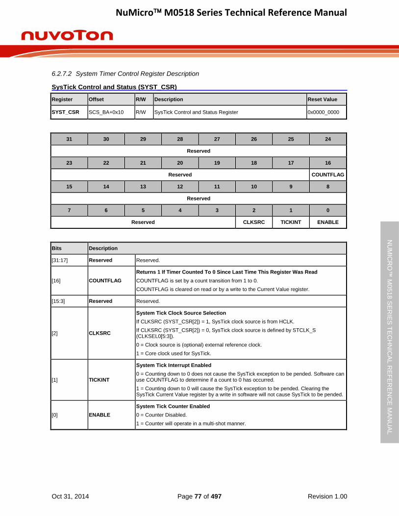
NuMicro M0518 Series Technical Reference Manual
Oct 31, 2014 Page 77 of 497 Revision 1.00
NU
MIC
RO
™ M
0518
SE
RIE
S T
EC
HN
ICA
L R
EF
ER
EN
CE
MA
NU
AL
6.2.7.2 System Timer Control Register Description
SysTick Control and Status (SYST_CSR)
Register Offset R/W Description Reset Value
SYST_CSR SCS_BA+0x10 R/W SysTick Control and Status Register 0x0000_0000
31 30 29 28 27 26 25 24
Reserved
23 22 21 20 19 18 17 16
Reserved COUNTFLAG
15 14 13 12 11 10 9 8
Reserved
7 6 5 4 3 2 1 0
Reserved CLKSRC TICKINT ENABLE
Bits Description
[31:17] Reserved Reserved.
[16] COUNTFLAG
Returns 1 If Timer Counted To 0 Since Last Time This Register Was Read
COUNTFLAG is set by a count transition from 1 to 0.
COUNTFLAG is cleared on read or by a write to the Current Value register.
[15:3] Reserved Reserved.
[2] CLKSRC
System Tick Clock Source Selection
If CLKSRC (SYST_CSR[2]) = 1, SysTick clock source is from HCLK.
If CLKSRC (SYST_CSR[2]) = 0, SysTick clock source is defined by STCLK_S (CLKSEL0[5:3]).
0 = Clock source is (optional) external reference clock.
1 = Core clock used for SysTick.
[1] TICKINT
System Tick Interrupt Enabled
0 = Counting down to 0 does not cause the SysTick exception to be pended. Software can use COUNTFLAG to determine if a count to 0 has occurred.
1 = Counting down to 0 will cause the SysTick exception to be pended. Clearing the SysTick Current Value register by a write in software will not cause SysTick to be pended.
[0] ENABLE
System Tick Counter Enabled
0 = Counter Disabled.
1 = Counter will operate in a multi-shot manner.
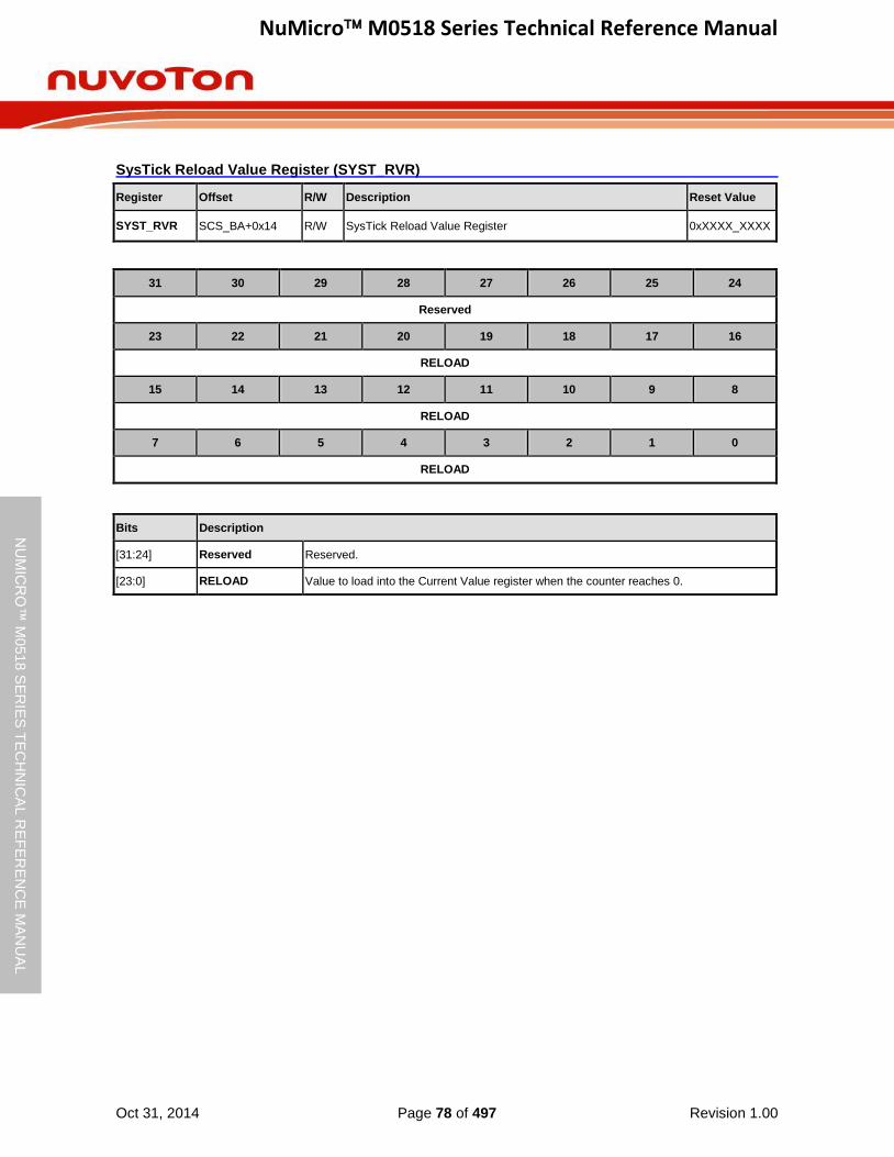
NuMicro M0518 Series Technical Reference Manual
Oct 31, 2014 Page 78 of 497 Revision 1.00
NU
MIC
RO
™ M
0518
SE
RIE
S T
EC
HN
ICA
L R
EF
ER
EN
CE
MA
NU
AL
SysTick Reload Value Register (SYST_RVR)
Register Offset R/W Description Reset Value
SYST_RVR SCS_BA+0x14 R/W SysTick Reload Value Register 0xXXXX_XXXX
31 30 29 28 27 26 25 24
Reserved
23 22 21 20 19 18 17 16
RELOAD
15 14 13 12 11 10 9 8
RELOAD
7 6 5 4 3 2 1 0
RELOAD
Bits Description
[31:24] Reserved Reserved.
[23:0] RELOAD Value to load into the Current Value register when the counter reaches 0.
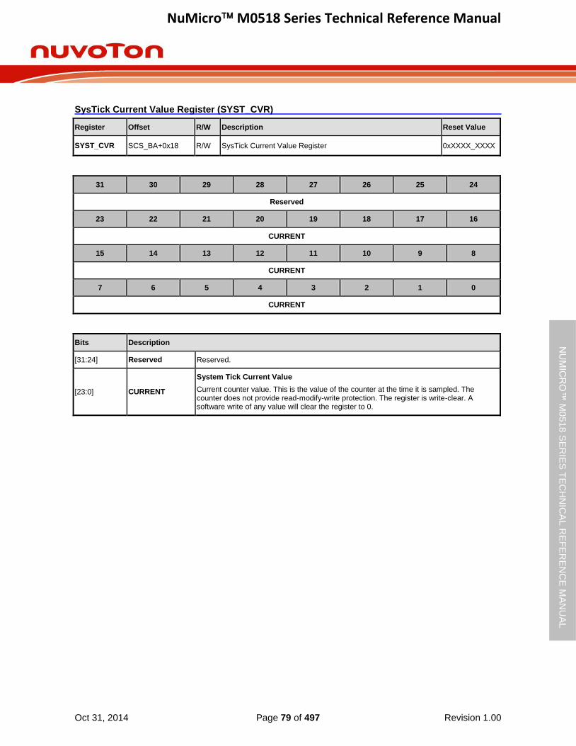
NuMicro M0518 Series Technical Reference Manual
Oct 31, 2014 Page 79 of 497 Revision 1.00
NU
MIC
RO
™ M
0518
SE
RIE
S T
EC
HN
ICA
L R
EF
ER
EN
CE
MA
NU
AL
SysTick Current Value Register (SYST_CVR)
Register Offset R/W Description Reset Value
SYST_CVR SCS_BA+0x18 R/W SysTick Current Value Register 0xXXXX_XXXX
31 30 29 28 27 26 25 24
Reserved
23 22 21 20 19 18 17 16
CURRENT
15 14 13 12 11 10 9 8
CURRENT
7 6 5 4 3 2 1 0
CURRENT
Bits Description
[31:24] Reserved Reserved.
[23:0] CURRENT
System Tick Current Value
Current counter value. This is the value of the counter at the time it is sampled. The counter does not provide read-modify-write protection. The register is write-clear. A software write of any value will clear the register to 0.
NuMicro M0518 Series Technical Reference Manual
Oct 31, 2014 Page 80 of 497 Revision 1.00
NU
MIC
RO
™ M
0518
SE
RIE
S T
EC
HN
ICA
L R
EF
ER
EN
CE
MA
NU
AL
6.2.8 Nested Vectored Interrupt Controller (NVIC)
The Cortex™-M0 provides an interrupt controller as an integral part of the exception mode, named as “Nested Vectored Interrupt Controller (NVIC)”, which is closely coupled to the processor core and provides following features:
Nested and Vectored interrupt support
Automatic processor state saving and restoration
Reduced and deterministic interrupt latency
The NVIC prioritizes and handles all supported exceptions. All exceptions are handled in “Handler Mode”. This NVIC architecture supports 32 (IRQ[31:0]) discrete interrupts with 4 levels of priority. All of the interrupts and most of the system exceptions can be configured to different priority levels. When an interrupt occurs, the NVIC will compare the priority of the new interrupt to the current running one’s priority. If the priority of the new interrupt is higher than the current one, the new interrupt handler will override the current handler.
When an interrupt is accepted, the starting address of the interrupt service routine (ISR) is fetched from a vector table in memory. There is no need to determine which interrupt is accepted and branch to the starting address of the correlated ISR by software. While the starting address is fetched, NVIC will also automatically save processor state including the registers “PC, PSR, LR, R0~R3, R12” to the stack. At the end of the ISR, the NVIC will restore the mentioned registers from stack and resume the normal execution. Thus it will take less and deterministic time to process the interrupt request.
The NVIC supports “Tail Chaining” which handles back-to-back interrupts efficiently without the overhead of states saving and restoration and therefore reduces delay time in switching to pending ISR at the end of current ISR. The NVIC also supports “Late Arrival” which improves the efficiency of concurrent ISRs. When a higher priority interrupt request occurs before the current ISR starts to execute (at the stage of state saving and starting address fetching), the NVIC will give priority to the higher one without delay penalty. Thus it advances the real-time capability.
For more detailed information, please refer to the “ARM® Cortex™-M0 Technical Reference
Manual” and “ARM® v6-M Architecture Reference Manual”.

NuMicro M0518 Series Technical Reference Manual
Oct 31, 2014 Page 81 of 497 Revision 1.00
NU
MIC
RO
™ M
0518
SE
RIE
S T
EC
HN
ICA
L R
EF
ER
EN
CE
MA
NU
AL
6.2.8.1 Exception Model and System Interrupt Map
The following table lists the exception model supported by NuMicro M0518 series. Software can set four levels of priority on some of these exceptions as well as on all interrupts. The highest user-configurable priority is denoted as “0” and the lowest priority is denoted as “3”. The default priority of all the user-configurable interrupts is “0”. Note that priority “0” is treated as the fourth priority on the system, after three system exceptions “Reset”, “NMI” and “Hard Fault”.
Exception Name Vector Number Priority
Reset 1 -3
NMI 2 -2
Hard Fault 3 -1
Reserved 4 ~ 10 Reserved
SVCall 11 Configurable
Reserved 12 ~ 13 Reserved
PendSV 14 Configurable
SysTick 15 Configurable
Interrupt (IRQ0 ~ IRQ31) 16 ~ 47 Configurable
Table 6-2 Exception Model
Vector Number
Interrupt Number
(Bit In Interrupt Registers)
Interrupt Name Source Module
Interrupt Description
1 ~ 15 - - - System exceptions
16 0 BOD_INT Brown-out Brown-out low voltage detected interrupt
17 1 WDT_INT WDT Watchdog Timer interrupt
18 2 EINT0 GPIO External signal interrupt from PB.14 pin
19 3 EINT1 GPIO External signal interrupt from PB.15 pin
20 4 GPAB_INT GPIO External signal interrupt from PA[15:0]/PB[13:0]
21 5 GPCDEF_INT GPIO External interrupt from PC[15:0]/PD[15:0]/PE[15:0]/PF[8:0]
22 6 - - Reserved
23 7 - - Reserved
24 8 TMR0_INT TMR0 Timer 0 interrupt
25 9 TMR1_INT TMR1 Timer 1 interrupt
26 10 TMR2_INT TMR2 Timer 2 interrupt
27 11 TMR3_INT TMR3 Timer 3 interrupt
28 12 UART02_INT UART0/2 UART0 and UART2 interrupt
29 13 UART1_INT UART1 UART1 interrupt

NuMicro M0518 Series Technical Reference Manual
Oct 31, 2014 Page 82 of 497 Revision 1.00
NU
MIC
RO
™ M
0518
SE
RIE
S T
EC
HN
ICA
L R
EF
ER
EN
CE
MA
NU
AL
30 14 SPI0_INT SPI0 SPI0 interrupt
31 15 UART3_INT UART3 UART3 interrupt
32 16 UART4_INT UART4 UART4 interrupt
33 17 UART5_INT UART5 UART5 interrupt
34 18 I2C0_INT I2C0 I
2C0 interrupt
35 19 I2C1_INT I2C1 I
2C1 interrupt
36 20 - - Reserved
37 21 - - Reserved
38 22 PWM0_INT PWM0 PWM0 interrupt
39 23 PWM1_INT PWM1 PWM1 interrupt
40 24 BPWM0_INT BPWM0 BPWM0 interrupt
41 25 BPWM1_INT BPWM1 BPWM1 interrupt
42 26 BRAKE0_INT PWM0 PWM0 brake interrupt
43 27 BRAKE1_INT PWM1 PWM1 brake interrupt
44 28 PWRWU_INT CLKC Clock controller interrupt for chip wake-up from Power-down state
45 29 ADC_INT ADC ADC interrupt
46 30 CKD_INT CLKC Clock detection interrupt
47 31 - - Reserved
Table 6-3 System Interrupt Map
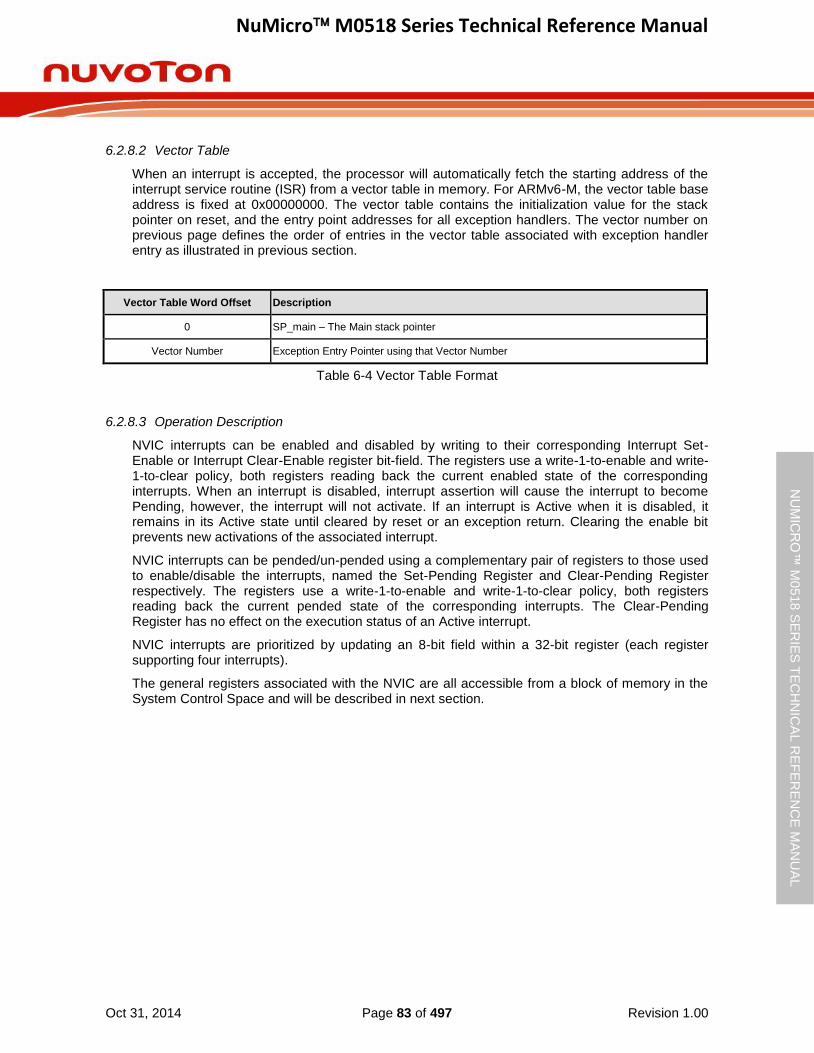
NuMicro M0518 Series Technical Reference Manual
Oct 31, 2014 Page 83 of 497 Revision 1.00
NU
MIC
RO
™ M
0518
SE
RIE
S T
EC
HN
ICA
L R
EF
ER
EN
CE
MA
NU
AL
6.2.8.2 Vector Table
When an interrupt is accepted, the processor will automatically fetch the starting address of the interrupt service routine (ISR) from a vector table in memory. For ARMv6-M, the vector table base address is fixed at 0x00000000. The vector table contains the initialization value for the stack pointer on reset, and the entry point addresses for all exception handlers. The vector number on previous page defines the order of entries in the vector table associated with exception handler entry as illustrated in previous section.
Vector Table Word Offset Description
0 SP_main – The Main stack pointer
Vector Number Exception Entry Pointer using that Vector Number
Table 6-4 Vector Table Format
6.2.8.3 Operation Description
NVIC interrupts can be enabled and disabled by writing to their corresponding Interrupt Set-Enable or Interrupt Clear-Enable register bit-field. The registers use a write-1-to-enable and write-1-to-clear policy, both registers reading back the current enabled state of the corresponding interrupts. When an interrupt is disabled, interrupt assertion will cause the interrupt to become Pending, however, the interrupt will not activate. If an interrupt is Active when it is disabled, it remains in its Active state until cleared by reset or an exception return. Clearing the enable bit prevents new activations of the associated interrupt.
NVIC interrupts can be pended/un-pended using a complementary pair of registers to those used to enable/disable the interrupts, named the Set-Pending Register and Clear-Pending Register respectively. The registers use a write-1-to-enable and write-1-to-clear policy, both registers reading back the current pended state of the corresponding interrupts. The Clear-Pending Register has no effect on the execution status of an Active interrupt.
NVIC interrupts are prioritized by updating an 8-bit field within a 32-bit register (each register supporting four interrupts).
The general registers associated with the NVIC are all accessible from a block of memory in the System Control Space and will be described in next section.
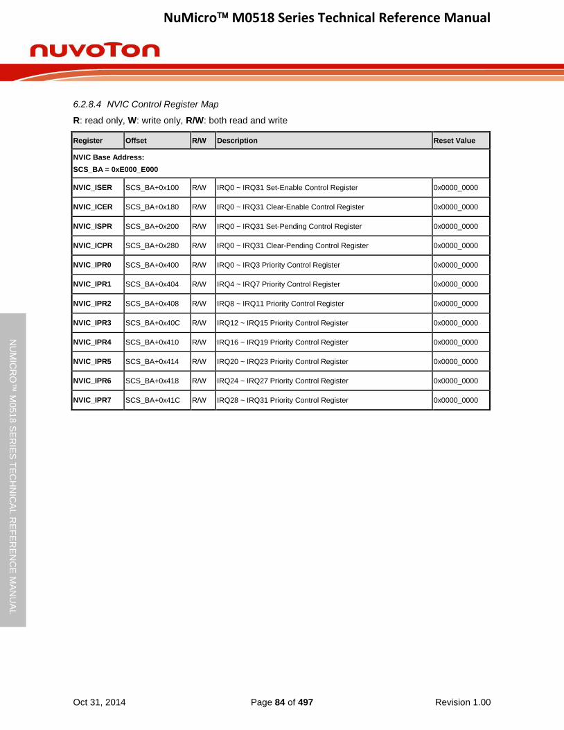
NuMicro M0518 Series Technical Reference Manual
Oct 31, 2014 Page 84 of 497 Revision 1.00
NU
MIC
RO
™ M
0518
SE
RIE
S T
EC
HN
ICA
L R
EF
ER
EN
CE
MA
NU
AL
6.2.8.4 NVIC Control Register Map
R: read only, W: write only, R/W: both read and write
Register Offset R/W Description Reset Value
NVIC Base Address:
SCS_BA = 0xE000_E000
NVIC_ISER SCS_BA+0x100 R/W IRQ0 ~ IRQ31 Set-Enable Control Register 0x0000_0000
NVIC_ICER SCS_BA+0x180 R/W IRQ0 ~ IRQ31 Clear-Enable Control Register 0x0000_0000
NVIC_ISPR SCS_BA+0x200 R/W IRQ0 ~ IRQ31 Set-Pending Control Register 0x0000_0000
NVIC_ICPR SCS_BA+0x280 R/W IRQ0 ~ IRQ31 Clear-Pending Control Register 0x0000_0000
NVIC_IPR0 SCS_BA+0x400 R/W IRQ0 ~ IRQ3 Priority Control Register 0x0000_0000
NVIC_IPR1 SCS_BA+0x404 R/W IRQ4 ~ IRQ7 Priority Control Register 0x0000_0000
NVIC_IPR2 SCS_BA+0x408 R/W IRQ8 ~ IRQ11 Priority Control Register 0x0000_0000
NVIC_IPR3 SCS_BA+0x40C R/W IRQ12 ~ IRQ15 Priority Control Register 0x0000_0000
NVIC_IPR4 SCS_BA+0x410 R/W IRQ16 ~ IRQ19 Priority Control Register 0x0000_0000
NVIC_IPR5 SCS_BA+0x414 R/W IRQ20 ~ IRQ23 Priority Control Register 0x0000_0000
NVIC_IPR6 SCS_BA+0x418 R/W IRQ24 ~ IRQ27 Priority Control Register 0x0000_0000
NVIC_IPR7 SCS_BA+0x41C R/W IRQ28 ~ IRQ31 Priority Control Register 0x0000_0000

NuMicro M0518 Series Technical Reference Manual
Oct 31, 2014 Page 85 of 497 Revision 1.00
NU
MIC
RO
™ M
0518
SE
RIE
S T
EC
HN
ICA
L R
EF
ER
EN
CE
MA
NU
AL
6.2.8.5 NVIC Control Register Description
IRQ0 ~ IRQ31 Set-Enable Control Register (NVIC_ISER)
Register Offset R/W Description Reset Value
NVIC_ISER SCS_BA+0x100 R/W IRQ0 ~ IRQ31 Set-Enable Control Register 0x0000_0000
31 30 29 28 27 26 25 24
SETENA
23 22 21 20 19 18 17 16
SETENA
15 14 13 12 11 10 9 8
SETENA
7 6 5 4 3 2 1 0
SETENA
Bits Description
[31:0] SETENA
Interrupt Enable Register
Enable one or more interrupts. Each bit represents an interrupt number from IRQ0 ~ IRQ31 (Vector number from 16 ~ 47).
Write Operation:
0 = No effect.
1 = Write 1 to enable associated interrupt.
Read Operation:
0 = Associated interrupt status is Disabled.
1 = Associated interrupt status is Enabled.
Read value indicates the current enable status.
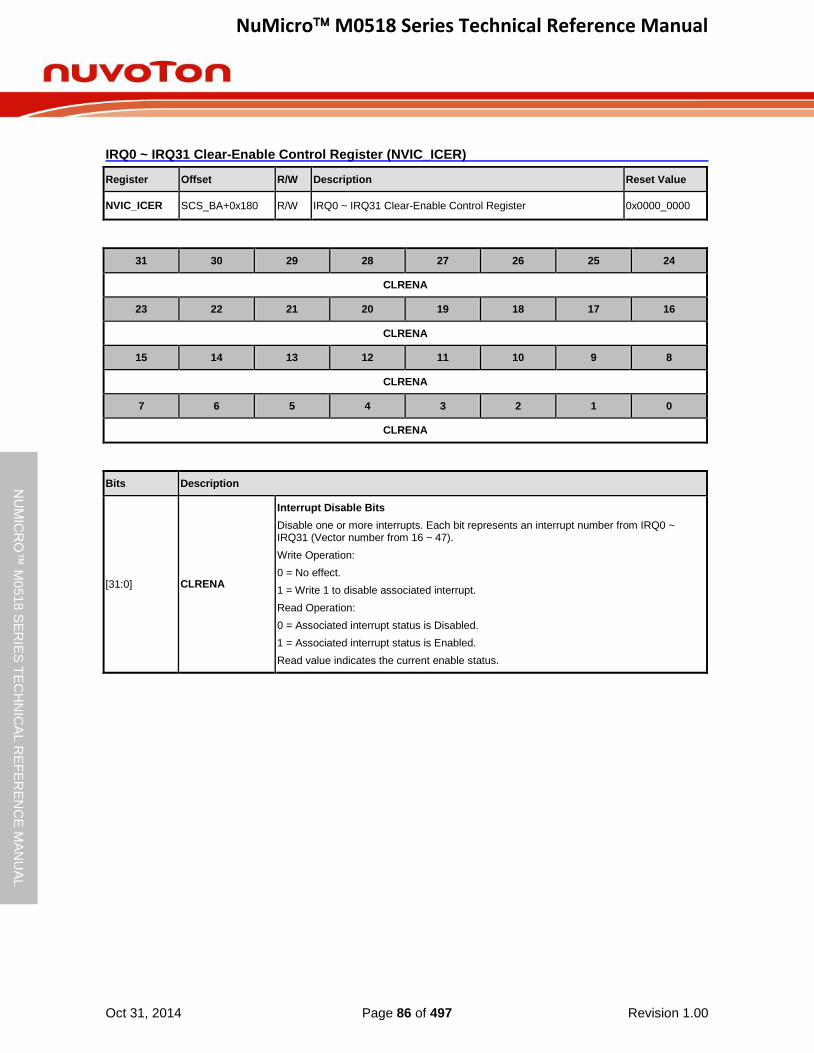
NuMicro M0518 Series Technical Reference Manual
Oct 31, 2014 Page 86 of 497 Revision 1.00
NU
MIC
RO
™ M
0518
SE
RIE
S T
EC
HN
ICA
L R
EF
ER
EN
CE
MA
NU
AL
IRQ0 ~ IRQ31 Clear-Enable Control Register (NVIC_ICER)
Register Offset R/W Description Reset Value
NVIC_ICER SCS_BA+0x180 R/W IRQ0 ~ IRQ31 Clear-Enable Control Register 0x0000_0000
31 30 29 28 27 26 25 24
CLRENA
23 22 21 20 19 18 17 16
CLRENA
15 14 13 12 11 10 9 8
CLRENA
7 6 5 4 3 2 1 0
CLRENA
Bits Description
[31:0] CLRENA
Interrupt Disable Bits
Disable one or more interrupts. Each bit represents an interrupt number from IRQ0 ~ IRQ31 (Vector number from 16 ~ 47).
Write Operation:
0 = No effect.
1 = Write 1 to disable associated interrupt.
Read Operation:
0 = Associated interrupt status is Disabled.
1 = Associated interrupt status is Enabled.
Read value indicates the current enable status.

NuMicro M0518 Series Technical Reference Manual
Oct 31, 2014 Page 87 of 497 Revision 1.00
NU
MIC
RO
™ M
0518
SE
RIE
S T
EC
HN
ICA
L R
EF
ER
EN
CE
MA
NU
AL
IRQ0 ~ IRQ31 Set-Pending Control Register (NVIC_ISPR)
Register Offset R/W Description Reset Value
NVIC_ISPR SCS_BA+0x200 R/W IRQ0 ~ IRQ31 Set-Pending Control Register 0x0000_0000
31 30 29 28 27 26 25 24
SETPEND
23 22 21 20 19 18 17 16
SETPEND
15 14 13 12 11 10 9 8
SETPEND
7 6 5 4 3 2 1 0
SETPEND
Bits Description
[31:0] SETPEND
Set Interrupt Pending Register
Write Operation:
0 = No effect.
1 = Write 1 to set pending state. Each bit represents an interrupt number from IRQ0 ~ IRQ31 (Vector number from 16 ~ 47).
Read Operation:
0 = Associated interrupt in not in pending status.
1 = Associated interrupt is in pending status.
Read value indicates the current pending status.

NuMicro M0518 Series Technical Reference Manual
Oct 31, 2014 Page 88 of 497 Revision 1.00
NU
MIC
RO
™ M
0518
SE
RIE
S T
EC
HN
ICA
L R
EF
ER
EN
CE
MA
NU
AL
IRQ0 ~ IRQ31 Clear-Pending Control Register (NVIC_ICPR)
Register Offset R/W Description Reset Value
NVIC_ICPR SCS_BA+0x280 R/W IRQ0 ~ IRQ31 Clear-Pending Control Register 0x0000_0000
31 30 29 28 27 26 25 24
CLRPEND
23 22 21 20 19 18 17 16
CLRPEND
15 14 13 12 11 10 9 8
CLRPEND
7 6 5 4 3 2 1 0
CLRPEND
Bits Description
[31:0] CLRPEND
Clear Interrupt Pending Register
Write Operation:
0 = No effect.
1 = Write 1 to clear pending state. Each bit represents an interrupt number from IRQ0 ~ IRQ31 (Vector number from 16 ~ 47).
Read Operation:
0 = Associated interrupt in not in pending status.
1 = Associated interrupt is in pending status.
Read value indicates the current pending status.

NuMicro M0518 Series Technical Reference Manual
Oct 31, 2014 Page 89 of 497 Revision 1.00
NU
MIC
RO
™ M
0518
SE
RIE
S T
EC
HN
ICA
L R
EF
ER
EN
CE
MA
NU
AL
IRQ0 ~ IRQ3 Priority Register (NVIC_IPR0)
Register Offset R/W Description Reset Value
NVIC_IPR0 SCS_BA+0x400 R/W IRQ0 ~ IRQ3 Priority Control Register 0x0000_0000
31 30 29 28 27 26 25 24
PRI_3 Reserved
23 22 21 20 19 18 17 16
PRI_2 Reserved
15 14 13 12 11 10 9 8
PRI_1 Reserved
7 6 5 4 3 2 1 0
PRI_0 Reserved
Bits Description
[31:30] PRI_3 Priority Of IRQ3
“0” denotes the highest priority and “3” denotes the lowest priority.
[29:24] Reserved Reserved.
[23:22] PRI_2 Priority Of IRQ2
“0” denotes the highest priority and “3” denotes the lowest priority.
[21:16] Reserved Reserved.
[15:14] PRI_1 Priority Of IRQ1
“0” denotes the highest priority and “3” denotes the lowest priority.
[13:8] Reserved Reserved.
[7:6] PRI_0 Priority Of IRQ0
“0” denotes the highest priority and “3” denotes the lowest priority.
[5:0] Reserved Reserved.

NuMicro M0518 Series Technical Reference Manual
Oct 31, 2014 Page 90 of 497 Revision 1.00
NU
MIC
RO
™ M
0518
SE
RIE
S T
EC
HN
ICA
L R
EF
ER
EN
CE
MA
NU
AL
IRQ4 ~ IRQ7 Priority Register (NVIC_IPR1)
Register Offset R/W Description Reset Value
NVIC_IPR1 SCS_BA+0x404 R/W IRQ4 ~ IRQ7 Priority Control Register 0x0000_0000
31 30 29 28 27 26 25 24
PRI_7 Reserved
23 22 21 20 19 18 17 16
PRI_6 Reserved
15 14 13 12 11 10 9 8
PRI_5 Reserved
7 6 5 4 3 2 1 0
PRI_4 Reserved
Bits Description
[31:30] PRI_7 Priority Of IRQ7
“0” denotes the highest priority and “3” denotes the lowest priority.
[29:24] Reserved Reserved.
[23:22] PRI_6 Priority Of IRQ6
“0” denotes the highest priority and “3” denotes the lowest priority.
[21:16] Reserved Reserved.
[15:14] PRI_5 Priority Of IRQ5
“0” denotes the highest priority and “3” denotes the lowest priority.
[13:8] Reserved Reserved.
[7:6] PRI_4 Priority Of IRQ4
“0” denotes the highest priority and “3” denotes the lowest priority.
[5:0] Reserved Reserved.

NuMicro M0518 Series Technical Reference Manual
Oct 31, 2014 Page 91 of 497 Revision 1.00
NU
MIC
RO
™ M
0518
SE
RIE
S T
EC
HN
ICA
L R
EF
ER
EN
CE
MA
NU
AL
IRQ8 ~ IRQ11 Priority Register (NVIC_IPR2)
Register Offset R/W Description Reset Value
NVIC_IPR2 SCS_BA+0x408 R/W IRQ8 ~ IRQ11 Priority Control Register 0x0000_0000
31 30 29 28 27 26 25 24
PRI_11 Reserved
23 22 21 20 19 18 17 16
PRI_10 Reserved
15 14 13 12 11 10 9 8
PRI_9 Reserved
7 6 5 4 3 2 1 0
PRI_8 Reserved
Bits Description
[31:30] PRI_11 Priority Of IRQ11
“0” denotes the highest priority and “3” denotes the lowest priority.
[29:24] Reserved Reserved.
[23:22] PRI_10 Priority Of IRQ10
“0” denotes the highest priority and “3” denotes the lowest priority.
[21:16] Reserved Reserved.
[15:14] PRI_9 Priority Of IRQ9
“0” denotes the highest priority and “3” denotes the lowest priority.
[13:8] Reserved Reserved.
[7:6] PRI_8 Priority Of IRQ8
“0” denotes the highest priority and “3” denotes the lowest priority.
[5:0] Reserved Reserved.

NuMicro M0518 Series Technical Reference Manual
Oct 31, 2014 Page 92 of 497 Revision 1.00
NU
MIC
RO
™ M
0518
SE
RIE
S T
EC
HN
ICA
L R
EF
ER
EN
CE
MA
NU
AL
IRQ12 ~ IRQ15 Priority Register (NVIC_IPR3)
Register Offset R/W Description Reset Value
NVIC_IPR3 SCS_BA+0x40C R/W IRQ12 ~ IRQ15 Priority Control Register 0x0000_0000
31 30 29 28 27 26 25 24
PRI_15 Reserved
23 22 21 20 19 18 17 16
PRI_14 Reserved
15 14 13 12 11 10 9 8
PRI_13 Reserved
7 6 5 4 3 2 1 0
PRI_12 Reserved
Bits Description
[31:30] PRI_15 Priority Of IRQ15
“0” denotes the highest priority and “3” denotes the lowest priority.
[29:24] Reserved Reserved.
[23:22] PRI_14 Priority Of IRQ14
“0” denotes the highest priority and “3” denotes the lowest priority.
[21:16] Reserved Reserved.
[15:14] PRI_13 Priority Of IRQ13
“0” denotes the highest priority and “3” denotes the lowest priority
[13:8] Reserved Reserved.
[7:6] PRI_12 Priority Of IRQ12
“0” denotes the highest priority and “3” denotes the lowest priority.
[5:0] Reserved Reserved.
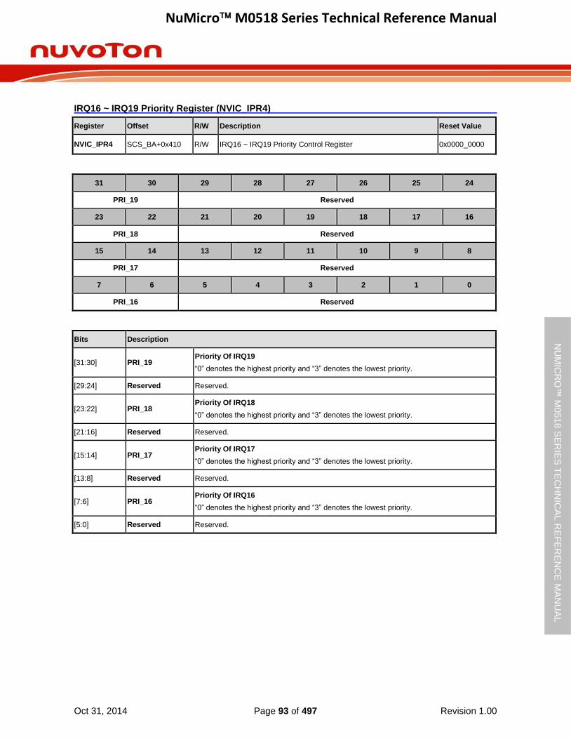
NuMicro M0518 Series Technical Reference Manual
Oct 31, 2014 Page 93 of 497 Revision 1.00
NU
MIC
RO
™ M
0518
SE
RIE
S T
EC
HN
ICA
L R
EF
ER
EN
CE
MA
NU
AL
IRQ16 ~ IRQ19 Priority Register (NVIC_IPR4)
Register Offset R/W Description Reset Value
NVIC_IPR4 SCS_BA+0x410 R/W IRQ16 ~ IRQ19 Priority Control Register 0x0000_0000
31 30 29 28 27 26 25 24
PRI_19 Reserved
23 22 21 20 19 18 17 16
PRI_18 Reserved
15 14 13 12 11 10 9 8
PRI_17 Reserved
7 6 5 4 3 2 1 0
PRI_16 Reserved
Bits Description
[31:30] PRI_19 Priority Of IRQ19
“0” denotes the highest priority and “3” denotes the lowest priority.
[29:24] Reserved Reserved.
[23:22] PRI_18 Priority Of IRQ18
“0” denotes the highest priority and “3” denotes the lowest priority.
[21:16] Reserved Reserved.
[15:14] PRI_17 Priority Of IRQ17
“0” denotes the highest priority and “3” denotes the lowest priority.
[13:8] Reserved Reserved.
[7:6] PRI_16 Priority Of IRQ16
“0” denotes the highest priority and “3” denotes the lowest priority.
[5:0] Reserved Reserved.

NuMicro M0518 Series Technical Reference Manual
Oct 31, 2014 Page 94 of 497 Revision 1.00
NU
MIC
RO
™ M
0518
SE
RIE
S T
EC
HN
ICA
L R
EF
ER
EN
CE
MA
NU
AL
IRQ20 ~ IRQ23 Priority Register (NVIC_IPR5)
Register Offset R/W Description Reset Value
NVIC_IPR5 SCS_BA+0x414 R/W IRQ20 ~ IRQ23 Priority Control Register 0x0000_0000
31 30 29 28 27 26 25 24
PRI_23 Reserved
23 22 21 20 19 18 17 16
PRI_22 Reserved
15 14 13 12 11 10 9 8
PRI_21 Reserved
7 6 5 4 3 2 1 0
PRI_20 Reserved
Bits Description
[31:30] PRI_23 Priority Of IRQ23
“0” denotes the highest priority and “3” denotes the lowest priority.
[29:24] Reserved Reserved.
[23:22] PRI_22 Priority Of IRQ22
“0” denotes the highest priority and “3” denotes the lowest priority.
[21:16] Reserved Reserved.
[15:14] PRI_21 Priority Of IRQ21
“0” denotes the highest priority and “3” denotes the lowest priority
[13:8] Reserved Reserved.
[7:6] PRI_20 Priority Of IRQ20
“0” denotes the highest priority and “3” denotes the lowest priority.
[5:0] Reserved Reserved.

NuMicro M0518 Series Technical Reference Manual
Oct 31, 2014 Page 95 of 497 Revision 1.00
NU
MIC
RO
™ M
0518
SE
RIE
S T
EC
HN
ICA
L R
EF
ER
EN
CE
MA
NU
AL
IRQ24 ~ IRQ27 Priority Register (NVIC_IPR6)
Register Offset R/W Description Reset Value
NVIC_IPR6 SCS_BA+0x418 R/W IRQ24 ~ IRQ27 Priority Control Register 0x0000_0000
31 30 29 28 27 26 25 24
PRI_27 Reserved
23 22 21 20 19 18 17 16
PRI_26 Reserved
15 14 13 12 11 10 9 8
PRI_25 Reserved
7 6 5 4 3 2 1 0
PRI_24 Reserved
Bits Description
[31:30] PRI_27 Priority Of IRQ27
“0” denotes the highest priority and “3” denotes the lowest priority.
[29:24] Reserved Reserved.
[23:22] PRI_26 Priority Of IRQ26
“0” denotes the highest priority and “3” denotes the lowest priority.
[21:16] Reserved Reserved.
[15:14] PRI_25 Priority Of IRQ25
“0” denotes the highest priority and “3” denotes the lowest priority.
[13:8] Reserved Reserved.
[7:6] PRI_24 Priority Of IRQ24
“0” denotes the highest priority and “3” denotes the lowest priority.
[5:0] Reserved Reserved.
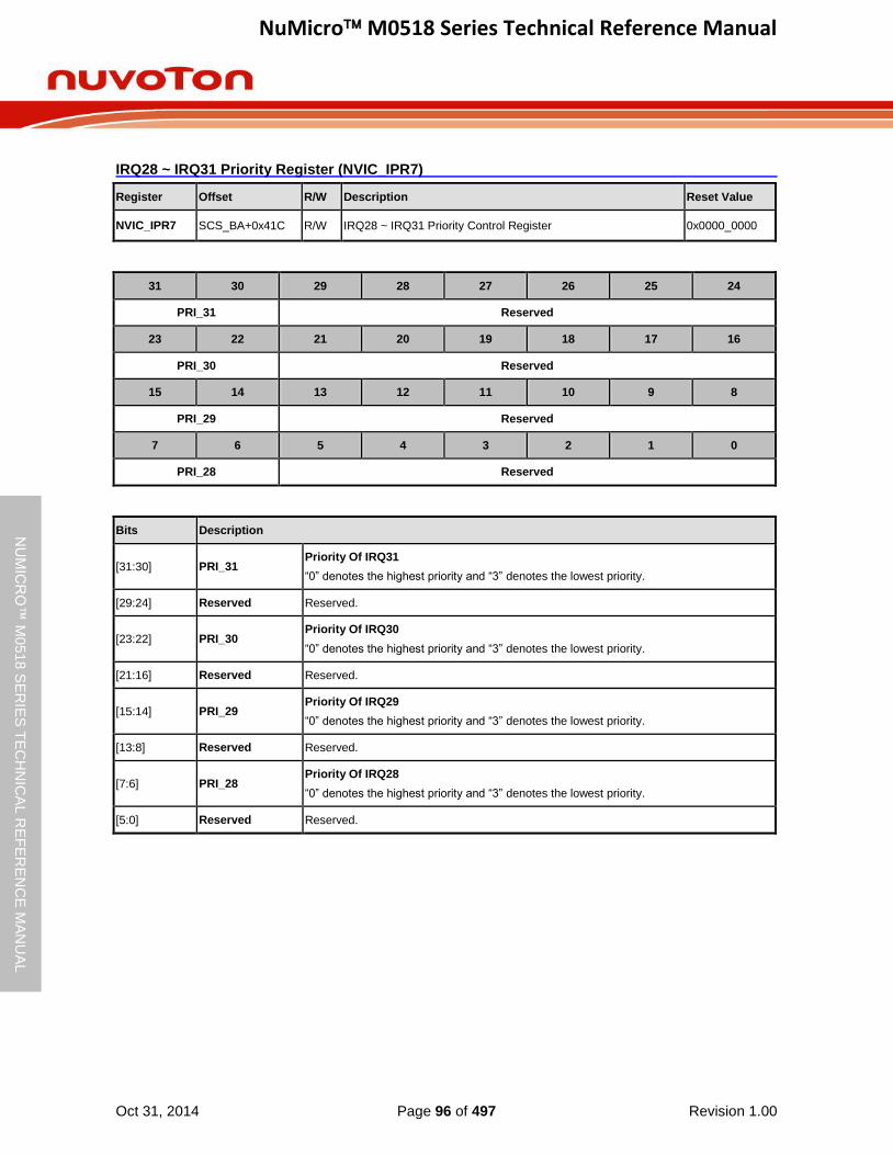
NuMicro M0518 Series Technical Reference Manual
Oct 31, 2014 Page 96 of 497 Revision 1.00
NU
MIC
RO
™ M
0518
SE
RIE
S T
EC
HN
ICA
L R
EF
ER
EN
CE
MA
NU
AL
IRQ28 ~ IRQ31 Priority Register (NVIC_IPR7)
Register Offset R/W Description Reset Value
NVIC_IPR7 SCS_BA+0x41C R/W IRQ28 ~ IRQ31 Priority Control Register 0x0000_0000
31 30 29 28 27 26 25 24
PRI_31 Reserved
23 22 21 20 19 18 17 16
PRI_30 Reserved
15 14 13 12 11 10 9 8
PRI_29 Reserved
7 6 5 4 3 2 1 0
PRI_28 Reserved
Bits Description
[31:30] PRI_31 Priority Of IRQ31
“0” denotes the highest priority and “3” denotes the lowest priority.
[29:24] Reserved Reserved.
[23:22] PRI_30 Priority Of IRQ30
“0” denotes the highest priority and “3” denotes the lowest priority.
[21:16] Reserved Reserved.
[15:14] PRI_29 Priority Of IRQ29
“0” denotes the highest priority and “3” denotes the lowest priority.
[13:8] Reserved Reserved.
[7:6] PRI_28 Priority Of IRQ28
“0” denotes the highest priority and “3” denotes the lowest priority.
[5:0] Reserved Reserved.
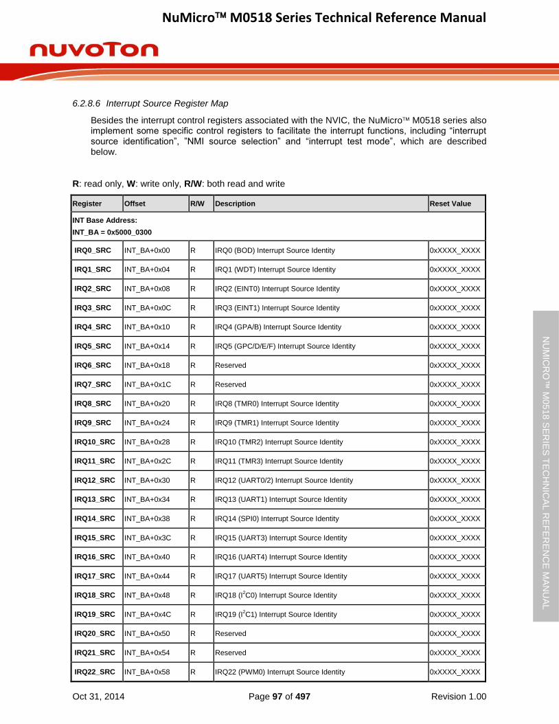
NuMicro M0518 Series Technical Reference Manual
Oct 31, 2014 Page 97 of 497 Revision 1.00
NU
MIC
RO
™ M
0518
SE
RIE
S T
EC
HN
ICA
L R
EF
ER
EN
CE
MA
NU
AL
6.2.8.6 Interrupt Source Register Map
Besides the interrupt control registers associated with the NVIC, the NuMicro M0518 series also implement some specific control registers to facilitate the interrupt functions, including “interrupt source identification”, ”NMI source selection” and “interrupt test mode”, which are described below.
R: read only, W: write only, R/W: both read and write
Register Offset R/W Description Reset Value
INT Base Address:
INT_BA = 0x5000_0300
IRQ0_SRC INT_BA+0x00 R IRQ0 (BOD) Interrupt Source Identity 0xXXXX_XXXX
IRQ1_SRC INT_BA+0x04 R IRQ1 (WDT) Interrupt Source Identity 0xXXXX_XXXX
IRQ2_SRC INT_BA+0x08 R IRQ2 (EINT0) Interrupt Source Identity 0xXXXX_XXXX
IRQ3_SRC INT_BA+0x0C R IRQ3 (EINT1) Interrupt Source Identity 0xXXXX_XXXX
IRQ4_SRC INT_BA+0x10 R IRQ4 (GPA/B) Interrupt Source Identity 0xXXXX_XXXX
IRQ5_SRC INT_BA+0x14 R IRQ5 (GPC/D/E/F) Interrupt Source Identity 0xXXXX_XXXX
IRQ6_SRC INT_BA+0x18 R Reserved 0xXXXX_XXXX
IRQ7_SRC INT_BA+0x1C R Reserved 0xXXXX_XXXX
IRQ8_SRC INT_BA+0x20 R IRQ8 (TMR0) Interrupt Source Identity 0xXXXX_XXXX
IRQ9_SRC INT_BA+0x24 R IRQ9 (TMR1) Interrupt Source Identity 0xXXXX_XXXX
IRQ10_SRC INT_BA+0x28 R IRQ10 (TMR2) Interrupt Source Identity 0xXXXX_XXXX
IRQ11_SRC INT_BA+0x2C R IRQ11 (TMR3) Interrupt Source Identity 0xXXXX_XXXX
IRQ12_SRC INT_BA+0x30 R IRQ12 (UART0/2) Interrupt Source Identity 0xXXXX_XXXX
IRQ13_SRC INT_BA+0x34 R IRQ13 (UART1) Interrupt Source Identity 0xXXXX_XXXX
IRQ14_SRC INT_BA+0x38 R IRQ14 (SPI0) Interrupt Source Identity 0xXXXX_XXXX
IRQ15_SRC INT_BA+0x3C R IRQ15 (UART3) Interrupt Source Identity 0xXXXX_XXXX
IRQ16_SRC INT_BA+0x40 R IRQ16 (UART4) Interrupt Source Identity 0xXXXX_XXXX
IRQ17_SRC INT_BA+0x44 R IRQ17 (UART5) Interrupt Source Identity 0xXXXX_XXXX
IRQ18_SRC INT_BA+0x48 R IRQ18 (I2C0) Interrupt Source Identity 0xXXXX_XXXX
IRQ19_SRC INT_BA+0x4C R IRQ19 (I2C1) Interrupt Source Identity 0xXXXX_XXXX
IRQ20_SRC INT_BA+0x50 R Reserved 0xXXXX_XXXX
IRQ21_SRC INT_BA+0x54 R Reserved 0xXXXX_XXXX
IRQ22_SRC INT_BA+0x58 R IRQ22 (PWM0) Interrupt Source Identity 0xXXXX_XXXX

NuMicro M0518 Series Technical Reference Manual
Oct 31, 2014 Page 98 of 497 Revision 1.00
NU
MIC
RO
™ M
0518
SE
RIE
S T
EC
HN
ICA
L R
EF
ER
EN
CE
MA
NU
AL
IRQ23_SRC INT_BA+0x5C R IRQ23 (PWM1) Interrupt Source Identity 0xXXXX_XXXX
IRQ24_SRC INT_BA+0x60 R IRQ24 (BPWM0) Interrupt Source Identity 0xXXXX_XXXX
IRQ25_SRC INT_BA+0x64 R IRQ25 (BPWM1) Interrupt Source Identity 0xXXXX_XXXX
IRQ26_SRC INT_BA+0x68 R IRQ26 (BRAKE0) Interrupt Source Identity 0xXXXX_XXXX
IRQ27_SRC INT_BA+0x6C R IRQ27 (BRAKE1) Interrupt Source Identity 0xXXXX_XXXX
IRQ28_SRC INT_BA+0x70 R IRQ28 (PWRWU) Interrupt Source Identity 0xXXXX_XXXX
IRQ29_SRC INT_BA+0x74 R IRQ29 (ADC) Interrupt Source Identity 0xXXXX_XXXX
IRQ30_SRC INT_BA+0x78 R IRQ30 (CKD) Interrupt Source Identity 0xXXXX_XXXX
IRQ31_SRC INT_BA+0x7C R Reserved 0xXXXX_XXXX
NMI_SEL INT_BA+0x80 R/W NMI Source Interrupt Select Control Register 0x0000_0000
MCU_IRQ INT_BA+0x84 R/W MCU Interrupt Request Source Register 0x0000_0000
MCU_IRQCR INT_BA+0x88 R/W MCU Interrupt Request Control Register 0x0000_0000
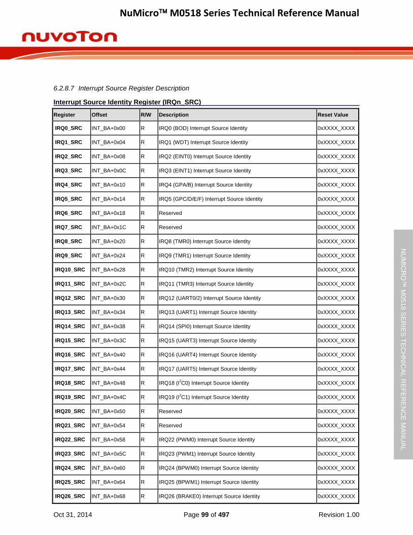
NuMicro M0518 Series Technical Reference Manual
Oct 31, 2014 Page 99 of 497 Revision 1.00
NU
MIC
RO
™ M
0518
SE
RIE
S T
EC
HN
ICA
L R
EF
ER
EN
CE
MA
NU
AL
6.2.8.7 Interrupt Source Register Description
Interrupt Source Identity Register (IRQn_SRC)
Register Offset R/W Description Reset Value
IRQ0_SRC INT_BA+0x00 R IRQ0 (BOD) Interrupt Source Identity 0xXXXX_XXXX
IRQ1_SRC INT_BA+0x04 R IRQ1 (WDT) Interrupt Source Identity 0xXXXX_XXXX
IRQ2_SRC INT_BA+0x08 R IRQ2 (EINT0) Interrupt Source Identity 0xXXXX_XXXX
IRQ3_SRC INT_BA+0x0C R IRQ3 (EINT1) Interrupt Source Identity 0xXXXX_XXXX
IRQ4_SRC INT_BA+0x10 R IRQ4 (GPA/B) Interrupt Source Identity 0xXXXX_XXXX
IRQ5_SRC INT_BA+0x14 R IRQ5 (GPC/D/E/F) Interrupt Source Identity 0xXXXX_XXXX
IRQ6_SRC INT_BA+0x18 R Reserved 0xXXXX_XXXX
IRQ7_SRC INT_BA+0x1C R Reserved 0xXXXX_XXXX
IRQ8_SRC INT_BA+0x20 R IRQ8 (TMR0) Interrupt Source Identity 0xXXXX_XXXX
IRQ9_SRC INT_BA+0x24 R IRQ9 (TMR1) Interrupt Source Identity 0xXXXX_XXXX
IRQ10_SRC INT_BA+0x28 R IRQ10 (TMR2) Interrupt Source Identity 0xXXXX_XXXX
IRQ11_SRC INT_BA+0x2C R IRQ11 (TMR3) Interrupt Source Identity 0xXXXX_XXXX
IRQ12_SRC INT_BA+0x30 R IRQ12 (UART0/2) Interrupt Source Identity 0xXXXX_XXXX
IRQ13_SRC INT_BA+0x34 R IRQ13 (UART1) Interrupt Source Identity 0xXXXX_XXXX
IRQ14_SRC INT_BA+0x38 R IRQ14 (SPI0) Interrupt Source Identity 0xXXXX_XXXX
IRQ15_SRC INT_BA+0x3C R IRQ15 (UART3) Interrupt Source Identity 0xXXXX_XXXX
IRQ16_SRC INT_BA+0x40 R IRQ16 (UART4) Interrupt Source Identity 0xXXXX_XXXX
IRQ17_SRC INT_BA+0x44 R IRQ17 (UART5) Interrupt Source Identity 0xXXXX_XXXX
IRQ18_SRC INT_BA+0x48 R IRQ18 (I2C0) Interrupt Source Identity 0xXXXX_XXXX
IRQ19_SRC INT_BA+0x4C R IRQ19 (I2C1) Interrupt Source Identity 0xXXXX_XXXX
IRQ20_SRC INT_BA+0x50 R Reserved 0xXXXX_XXXX
IRQ21_SRC INT_BA+0x54 R Reserved 0xXXXX_XXXX
IRQ22_SRC INT_BA+0x58 R IRQ22 (PWM0) Interrupt Source Identity 0xXXXX_XXXX
IRQ23_SRC INT_BA+0x5C R IRQ23 (PWM1) Interrupt Source Identity 0xXXXX_XXXX
IRQ24_SRC INT_BA+0x60 R IRQ24 (BPWM0) Interrupt Source Identity 0xXXXX_XXXX
IRQ25_SRC INT_BA+0x64 R IRQ25 (BPWM1) Interrupt Source Identity 0xXXXX_XXXX
IRQ26_SRC INT_BA+0x68 R IRQ26 (BRAKE0) Interrupt Source Identity 0xXXXX_XXXX
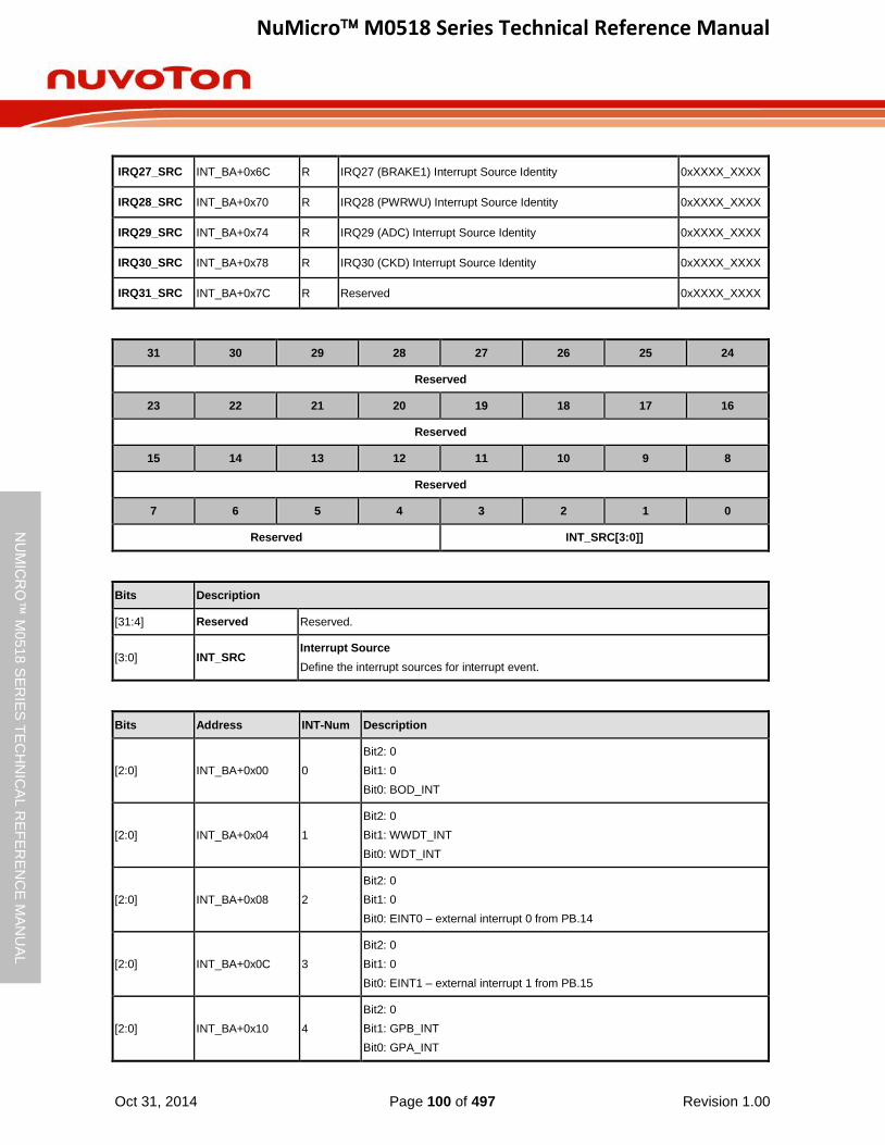
NuMicro M0518 Series Technical Reference Manual
Oct 31, 2014 Page 100 of 497 Revision 1.00
NU
MIC
RO
™ M
0518
SE
RIE
S T
EC
HN
ICA
L R
EF
ER
EN
CE
MA
NU
AL
IRQ27_SRC INT_BA+0x6C R IRQ27 (BRAKE1) Interrupt Source Identity 0xXXXX_XXXX
IRQ28_SRC INT_BA+0x70 R IRQ28 (PWRWU) Interrupt Source Identity 0xXXXX_XXXX
IRQ29_SRC INT_BA+0x74 R IRQ29 (ADC) Interrupt Source Identity 0xXXXX_XXXX
IRQ30_SRC INT_BA+0x78 R IRQ30 (CKD) Interrupt Source Identity 0xXXXX_XXXX
IRQ31_SRC INT_BA+0x7C R Reserved 0xXXXX_XXXX
31 30 29 28 27 26 25 24
Reserved
23 22 21 20 19 18 17 16
Reserved
15 14 13 12 11 10 9 8
Reserved
7 6 5 4 3 2 1 0
Reserved INT_SRC[3:0]]
Bits Description
[31:4] Reserved Reserved.
[3:0] INT_SRC Interrupt Source
Define the interrupt sources for interrupt event.
Bits Address INT-Num Description
[2:0] INT_BA+0x00 0
Bit2: 0
Bit1: 0
Bit0: BOD_INT
[2:0] INT_BA+0x04 1
Bit2: 0
Bit1: WWDT_INT
Bit0: WDT_INT
[2:0] INT_BA+0x08 2
Bit2: 0
Bit1: 0
Bit0: EINT0 – external interrupt 0 from PB.14
[2:0] INT_BA+0x0C 3
Bit2: 0
Bit1: 0
Bit0: EINT1 – external interrupt 1 from PB.15
[2:0] INT_BA+0x10 4
Bit2: 0
Bit1: GPB_INT
Bit0: GPA_INT
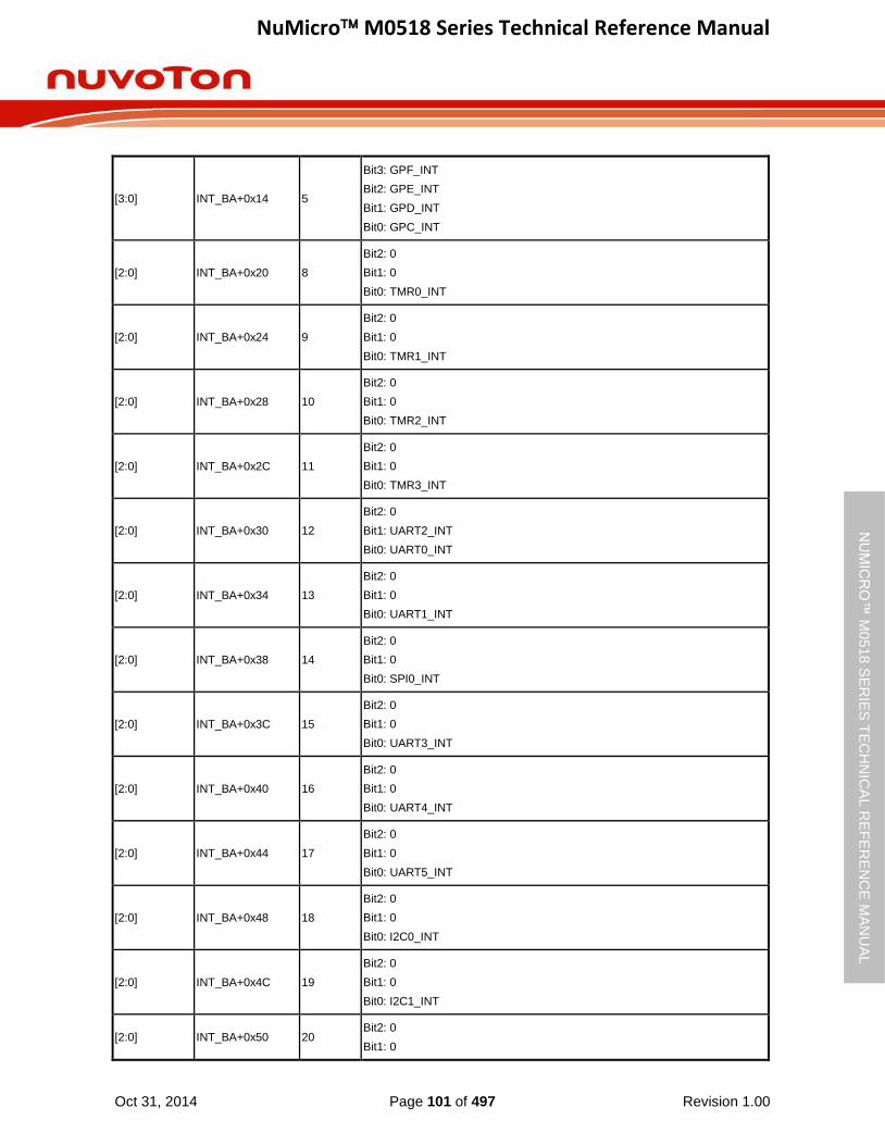
NuMicro M0518 Series Technical Reference Manual
Oct 31, 2014 Page 101 of 497 Revision 1.00
NU
MIC
RO
™ M
0518
SE
RIE
S T
EC
HN
ICA
L R
EF
ER
EN
CE
MA
NU
AL
[3:0] INT_BA+0x14 5
Bit3: GPF_INT
Bit2: GPE_INT
Bit1: GPD_INT
Bit0: GPC_INT
[2:0] INT_BA+0x20 8
Bit2: 0
Bit1: 0
Bit0: TMR0_INT
[2:0] INT_BA+0x24 9
Bit2: 0
Bit1: 0
Bit0: TMR1_INT
[2:0] INT_BA+0x28 10
Bit2: 0
Bit1: 0
Bit0: TMR2_INT
[2:0] INT_BA+0x2C 11
Bit2: 0
Bit1: 0
Bit0: TMR3_INT
[2:0] INT_BA+0x30 12
Bit2: 0
Bit1: UART2_INT
Bit0: UART0_INT
[2:0] INT_BA+0x34 13
Bit2: 0
Bit1: 0
Bit0: UART1_INT
[2:0] INT_BA+0x38 14
Bit2: 0
Bit1: 0
Bit0: SPI0_INT
[2:0] INT_BA+0x3C 15
Bit2: 0
Bit1: 0
Bit0: UART3_INT
[2:0] INT_BA+0x40 16
Bit2: 0
Bit1: 0
Bit0: UART4_INT
[2:0] INT_BA+0x44 17
Bit2: 0
Bit1: 0
Bit0: UART5_INT
[2:0] INT_BA+0x48 18
Bit2: 0
Bit1: 0
Bit0: I2C0_INT
[2:0] INT_BA+0x4C 19
Bit2: 0
Bit1: 0
Bit0: I2C1_INT
[2:0] INT_BA+0x50 20 Bit2: 0
Bit1: 0
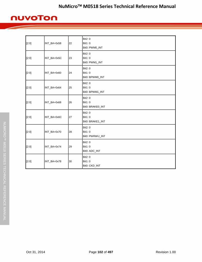
NuMicro M0518 Series Technical Reference Manual
Oct 31, 2014 Page 102 of 497 Revision 1.00
NU
MIC
RO
™ M
0518
SE
RIE
S T
EC
HN
ICA
L R
EF
ER
EN
CE
MA
NU
AL
[2:0] INT_BA+0x58 22
Bit2: 0
Bit1: 0
Bit0: PWM0_INT
[2:0] INT_BA+0x5C 23
Bit2: 0
Bit1: 0
Bit0: PWM1_INT
[2:0] INT_BA+0x60 24
Bit2: 0
Bit1: 0
Bit0: BPWM0_INT
[2:0] INT_BA+0x64 25
Bit2: 0
Bit1: 0
Bit0: BPWM1_INT
[2:0] INT_BA+0x68 26
Bit2: 0
Bit1: 0
Bit0: BRAKE0_INT
[2:0] INT_BA+0x6C 27
Bit2: 0
Bit1: 0
Bit0: BRAKE1_INT
[2:0] INT_BA+0x70 28
Bit2: 0
Bit1: 0
Bit0: PWRWU_INT
[2:0] INT_BA+0x74 29
Bit2: 0
Bit1: 0
Bit0: ADC_INT
[2:0] INT_BA+0x78 30
Bit2: 0
Bit1: 0
Bit0: CKD_INT

NuMicro M0518 Series Technical Reference Manual
Oct 31, 2014 Page 103 of 497 Revision 1.00
NU
MIC
RO
™ M
0518
SE
RIE
S T
EC
HN
ICA
L R
EF
ER
EN
CE
MA
NU
AL
NMI Source Interrupt Select Control Register (NMI_SEL)
Register Offset R/W Description Reset Value
NMI_SEL INT_BA+0x80 R/W NMI Source Interrupt Select Control Register 0x0000_0000
31 30 29 28 27 26 25 24
Reserved
23 22 21 20 19 18 17 16
Reserved
15 14 13 12 11 10 9 8
Reserved NMI_EN
7 6 5 4 3 2 1 0
Reserved NMI_SEL
Bits Description
[31:9] Reserved Reserved.
[8] NMI_EN
NMI Interrupt Enable Bit (Write Protect)
0 = NMI interrupt Disabled.
1 = NMI interrupt Enabled.
Note: This bit is the protected bit, and programming it needs to write “59h”, “16h”, and “88h” to address 0x5000_0100 to disable register protection. Refer to the register REGWRPROT at address GCR_BA+0x100.
[7:5] Reserved Reserved.
[4:0] NMI_SEL
NMI Interrupt Source Selection
The NMI interrupt to Cortex™-M0 can be selected from one of the peripheral interrupt by setting NMI_SEL.

NuMicro M0518 Series Technical Reference Manual
Oct 31, 2014 Page 104 of 497 Revision 1.00
NU
MIC
RO
™ M
0518
SE
RIE
S T
EC
HN
ICA
L R
EF
ER
EN
CE
MA
NU
AL
MCU Interrupt Request Source Register (MCU_IRQ)
Register Offset R/W Description Reset Value
MCU_IRQ INT_BA+0x84 R/W MCU Interrupt Request Source Register 0x0000_0000
31 30 29 28 27 26 25 24
MCU_IRQ
23 22 21 20 19 18 17 16
MCU_IRQ
15 14 13 12 11 10 9 8
MCU_IRQ
7 6 5 4 3 2 1 0
MCU_IRQ
Bits Description
[31:0] MCU_IRQ
MCU IRQ Source Register
The MCU_IRQ collects all the interrupts from the peripherals and generates the synchronous interrupt to Cortex™-M0. There are two modes to generate interrupt to Cortex™-M0, the normal mode and test mode.
The MCU_IRQ collects all interrupts from each peripheral and synchronizes them and interrupts the Cortex™-M0.
When the MCU_IRQ[n] is 0: Set MCU_IRQ[n] 1 will generate an interrupt to Cortex™-M0 NVIC[n].
When the MCU_IRQ[n] is 1 (mean an interrupt is assert), setting 1 to the MCU_IRQ[n] 1 will clear the interrupt and setting MCU_IRQ[n] 0: has no effect.
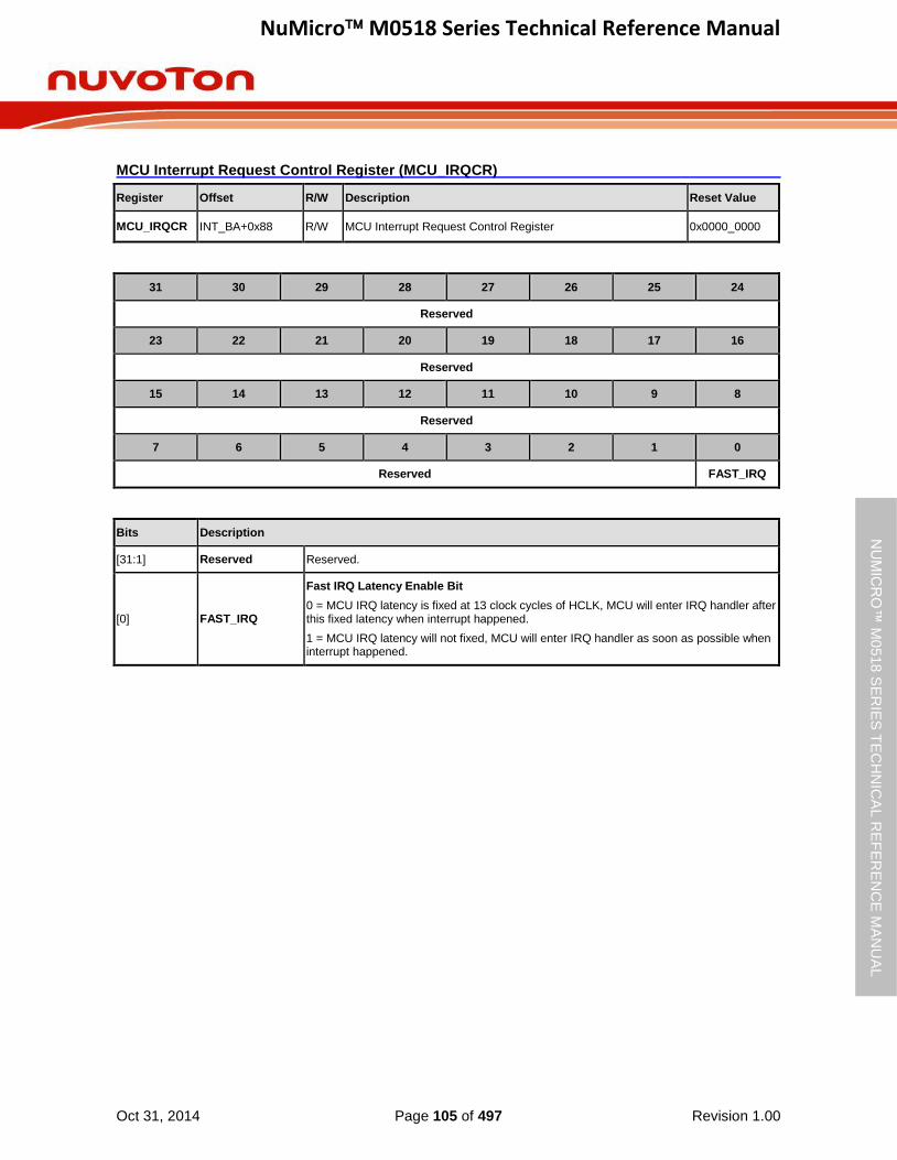
NuMicro M0518 Series Technical Reference Manual
Oct 31, 2014 Page 105 of 497 Revision 1.00
NU
MIC
RO
™ M
0518
SE
RIE
S T
EC
HN
ICA
L R
EF
ER
EN
CE
MA
NU
AL
MCU Interrupt Request Control Register (MCU_IRQCR)
Register Offset R/W Description Reset Value
MCU_IRQCR INT_BA+0x88 R/W MCU Interrupt Request Control Register 0x0000_0000
31 30 29 28 27 26 25 24
Reserved
23 22 21 20 19 18 17 16
Reserved
15 14 13 12 11 10 9 8
Reserved
7 6 5 4 3 2 1 0
Reserved FAST_IRQ
Bits Description
[31:1] Reserved Reserved.
[0] FAST_IRQ
Fast IRQ Latency Enable Bit
0 = MCU IRQ latency is fixed at 13 clock cycles of HCLK, MCU will enter IRQ handler after this fixed latency when interrupt happened.
1 = MCU IRQ latency will not fixed, MCU will enter IRQ handler as soon as possible when interrupt happened.

NuMicro M0518 Series Technical Reference Manual
Oct 31, 2014 Page 106 of 497 Revision 1.00
NU
MIC
RO
™ M
0518
SE
RIE
S T
EC
HN
ICA
L R
EF
ER
EN
CE
MA
NU
AL
6.2.9 System Control
The Cortex™-M0 status and operating mode control are managed by System Control Registers. Including CPUID, Cortex™-M0 interrupt priority and Cortex™-M0 power management can be controlled through these system control registers.
For more detailed information, please refer to the “ARM® Cortex™-M0 Technical Reference
Manual” and “ARM® v6-M Architecture Reference Manual”.
6.2.9.1 System Control Register Map
R: read only, W: write only, R/W: both read and write
Register Offset R/W Description Reset Value
SCS Base Address:
SCS_BA = 0xE000_E000
CPUID SCS_BA+0xD00 R CPUID Register 0x410C_C200
ICSR SCS_BA+0xD04 R/W Interrupt Control and State Register 0x0000_0000
AIRCR SCS_BA+0xD0C R/W Application Interrupt and Reset Control Register 0xFA05_0000
SCR SCS_BA+0xD10 R/W System Control Register 0x0000_0000
SHPR2 SCS_BA+0xD1C R/W System Handler Priority Register 2 0x0000_0000
SHPR3 SCS_BA+0xD20 R/W System Handler Priority Register 3 0x0000_0000

NuMicro M0518 Series Technical Reference Manual
Oct 31, 2014 Page 107 of 497 Revision 1.00
NU
MIC
RO
™ M
0518
SE
RIE
S T
EC
HN
ICA
L R
EF
ER
EN
CE
MA
NU
AL
6.2.9.2 System Control Register Description
CPUID Register (CPUID)
Register Offset R/W Description Reset Value
CPUID SCS_BA+0xD00 R CPUID Register 0x410C_C200
31 30 29 28 27 26 25 24
IMPLEMENTER[7:0]
23 22 21 20 19 18 17 16
Reserved PART[3:0]
15 14 13 12 11 10 9 8
PARTNO[11:4]
7 6 5 4 3 2 1 0
PARTNO[3:0] REVISION[3:0]
Bits Description
[31:24] IMPLEMENTER Implementer Code Assigned By ARM
Implementer code assigned by ARM. (ARM = 0x41).
[23:20] Reserved Reserved.
[19:16] PART Architecture Of The Processor
Read as 0xC for ARMv6-M parts.
[15:4] PARTNO Part Number Of The Processor
Read as 0xC20.
[3:0] REVISION Revision Number
Read as 0x0.

NuMicro M0518 Series Technical Reference Manual
Oct 31, 2014 Page 108 of 497 Revision 1.00
NU
MIC
RO
™ M
0518
SE
RIE
S T
EC
HN
ICA
L R
EF
ER
EN
CE
MA
NU
AL
Interrupt Control State Register (ICSR)
Register Offset R/W Description Reset Value
ICSR SCS_BA+0xD04 R/W Interrupt Control and State Register 0x0000_0000
31 30 29 28 27 26 25 24
NMIPENDSET Reserved PENDSVSET PENDSVCLR PENDSTSET PENDSTCLR Reserved
23 22 21 20 19 18 17 16
ISRPREEMPT ISRPENDING Reserved VECTPENDING[5:4]
15 14 13 12 11 10 9 8
VECTPENDING[3:0] Reserved
7 6 5 4 3 2 1 0
Reserved VECTACTIVE[5:0]
Bits Description
[31] NMIPENDSET
NMI Set-Pending Bit
Write Operation:
0 = No effect.
1 = Changes NMI exception state to pending.
Read Operation:
0 = NMI exception not pending.
1 = NMI exception pending.
Because NMI is the highest-priority exception, normally the processor enters the NMI exception handler as soon as it detects a write of 1 to this bit. Entering the handler then clears this bit to 0. This means a read of this bit by the NMI exception handler returns 1 only if the NMI signal is reasserted while the processor is executing that handler.
[30:29] Reserved Reserved.
[28] PENDSVSET
PendSV Set-Pending Bit
Write Operation:
0 = No effect.
1 = Changes PendSV exception state to pending.
Read Operation:
0 = PendSV exception is not pending.
1 = PendSV exception is pending.
Note: Writing 1 to this bit is the only way to set the PendSV exception state to pending.
[27] PENDSVCLR
PendSV Clear-Pending Bit
Write Operation:
0 = No effect.
1 = Removes the pending state from the PendSV exception.
This is a write only bit. When you want to clear PENDSV bit, you must “write 0 to PENDSVSET and write 1 to PENDSVCLR” at the same time.
[26] PENDSTSET SysTick Exception Set-Pending Bit
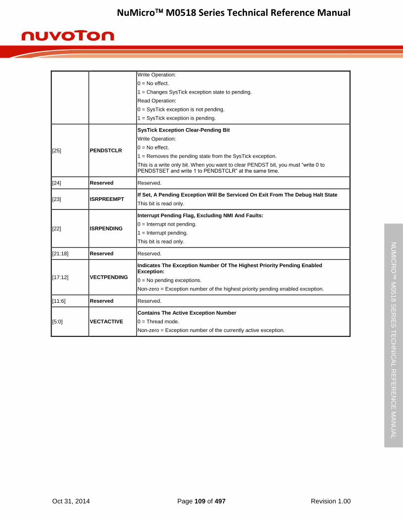
NuMicro M0518 Series Technical Reference Manual
Oct 31, 2014 Page 109 of 497 Revision 1.00
NU
MIC
RO
™ M
0518
SE
RIE
S T
EC
HN
ICA
L R
EF
ER
EN
CE
MA
NU
AL
Write Operation:
0 = No effect.
1 = Changes SysTick exception state to pending.
Read Operation:
0 = SysTick exception is not pending.
1 = SysTick exception is pending.
[25] PENDSTCLR
SysTick Exception Clear-Pending Bit
Write Operation:
0 = No effect.
1 = Removes the pending state from the SysTick exception.
This is a write only bit. When you want to clear PENDST bit, you must “write 0 to PENDSTSET and write 1 to PENDSTCLR” at the same time.
[24] Reserved Reserved.
[23] ISRPREEMPT If Set, A Pending Exception Will Be Serviced On Exit From The Debug Halt State
This bit is read only.
[22] ISRPENDING
Interrupt Pending Flag, Excluding NMI And Faults:
0 = Interrupt not pending.
1 = Interrupt pending.
This bit is read only.
[21:18] Reserved Reserved.
[17:12] VECTPENDING
Indicates The Exception Number Of The Highest Priority Pending Enabled Exception:
0 = No pending exceptions.
Non-zero = Exception number of the highest priority pending enabled exception.
[11:6] Reserved Reserved.
[5:0] VECTACTIVE
Contains The Active Exception Number
0 = Thread mode.
Non-zero = Exception number of the currently active exception.
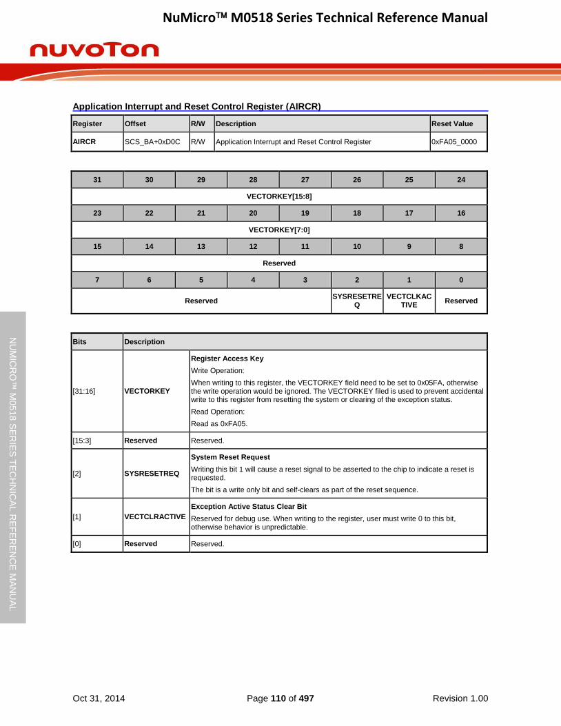
NuMicro M0518 Series Technical Reference Manual
Oct 31, 2014 Page 110 of 497 Revision 1.00
NU
MIC
RO
™ M
0518
SE
RIE
S T
EC
HN
ICA
L R
EF
ER
EN
CE
MA
NU
AL
Application Interrupt and Reset Control Register (AIRCR)
Register Offset R/W Description Reset Value
AIRCR SCS_BA+0xD0C R/W Application Interrupt and Reset Control Register 0xFA05_0000
31 30 29 28 27 26 25 24
VECTORKEY[15:8]
23 22 21 20 19 18 17 16
VECTORKEY[7:0]
15 14 13 12 11 10 9 8
Reserved
7 6 5 4 3 2 1 0
Reserved SYSRESETRE
Q VECTCLKAC
TIVE Reserved
Bits Description
[31:16] VECTORKEY
Register Access Key
Write Operation:
When writing to this register, the VECTORKEY field need to be set to 0x05FA, otherwise the write operation would be ignored. The VECTORKEY filed is used to prevent accidental write to this register from resetting the system or clearing of the exception status.
Read Operation:
Read as 0xFA05.
[15:3] Reserved Reserved.
[2] SYSRESETREQ
System Reset Request
Writing this bit 1 will cause a reset signal to be asserted to the chip to indicate a reset is requested.
The bit is a write only bit and self-clears as part of the reset sequence.
[1] VECTCLRACTIVE
Exception Active Status Clear Bit
Reserved for debug use. When writing to the register, user must write 0 to this bit, otherwise behavior is unpredictable.
[0] Reserved Reserved.

NuMicro M0518 Series Technical Reference Manual
Oct 31, 2014 Page 111 of 497 Revision 1.00
NU
MIC
RO
™ M
0518
SE
RIE
S T
EC
HN
ICA
L R
EF
ER
EN
CE
MA
NU
AL
System Control Register (SCR)
Register Offset R/W Description Reset Value
SCR SCS_BA+0xD10 R/W System Control Register 0x0000_0000
31 30 29 28 27 26 25 24
Reserved
23 22 21 20 19 18 17 16
Reserved
15 14 13 12 11 10 9 8
Reserved
7 6 5 4 3 2 1 0
Reserved SEVONPEND Reserved SLEEPDEEP SLEEPONEXIT Reserved
Bits Description
[31:5] Reserved Reserved.
[4] SEVONPEND
Send Event On Pending Bit
0 = Only enabled interrupts or events can wake-up the processor, disabled interrupts are excluded.
1 = Enabled events and all interrupts, including disabled interrupts, can wake-up the processor.
When an event or interrupt enters pending state, the event signal wakes up the processor from WFE. If the processor is not waiting for an event, the event is registered and affects the next WFE.
The processor also wakes up on execution of an SEV instruction or an external event.
[3] Reserved Reserved.
[2] SLEEPDEEP
Processor Deep Sleep And Sleep Mode Selection
Controls whether the processor uses sleep or deep sleep as its low power mode:
0 = Sleep mode.
1 = Deep Sleep mode.
[1] SLEEPONEXIT
Sleep-On-Exit Enable Bit
This bit indicates sleep-on-exit when returning from Handler mode to Thread mode.
0 = Do not sleep when returning to Thread mode.
1 = Enter Sleep or Deep Sleep when returning from ISR to Thread mode.
Setting this bit to 1 enables an interrupt driven application to avoid returning to an empty main application.
[0] Reserved Reserved.
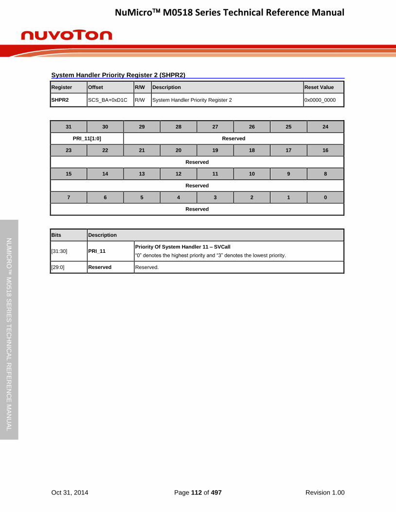
NuMicro M0518 Series Technical Reference Manual
Oct 31, 2014 Page 112 of 497 Revision 1.00
NU
MIC
RO
™ M
0518
SE
RIE
S T
EC
HN
ICA
L R
EF
ER
EN
CE
MA
NU
AL
System Handler Priority Register 2 (SHPR2)
Register Offset R/W Description Reset Value
SHPR2 SCS_BA+0xD1C R/W System Handler Priority Register 2 0x0000_0000
31 30 29 28 27 26 25 24
PRI_11[1:0] Reserved
23 22 21 20 19 18 17 16
Reserved
15 14 13 12 11 10 9 8
Reserved
7 6 5 4 3 2 1 0
Reserved
Bits Description
[31:30] PRI_11 Priority Of System Handler 11 – SVCall
“0” denotes the highest priority and “3” denotes the lowest priority.
[29:0] Reserved Reserved.
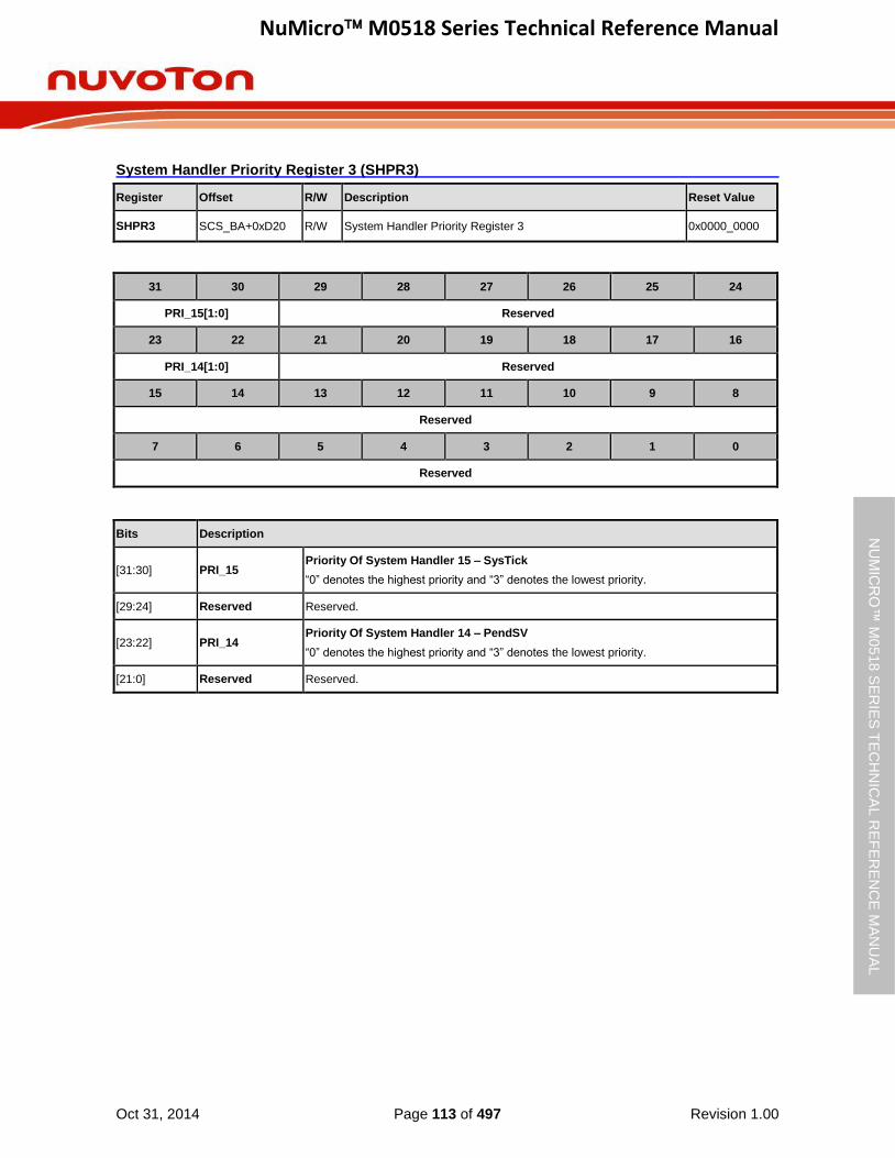
NuMicro M0518 Series Technical Reference Manual
Oct 31, 2014 Page 113 of 497 Revision 1.00
NU
MIC
RO
™ M
0518
SE
RIE
S T
EC
HN
ICA
L R
EF
ER
EN
CE
MA
NU
AL
System Handler Priority Register 3 (SHPR3)
Register Offset R/W Description Reset Value
SHPR3 SCS_BA+0xD20 R/W System Handler Priority Register 3 0x0000_0000
31 30 29 28 27 26 25 24
PRI_15[1:0] Reserved
23 22 21 20 19 18 17 16
PRI_14[1:0] Reserved
15 14 13 12 11 10 9 8
Reserved
7 6 5 4 3 2 1 0
Reserved
Bits Description
[31:30] PRI_15 Priority Of System Handler 15 – SysTick
“0” denotes the highest priority and “3” denotes the lowest priority.
[29:24] Reserved Reserved.
[23:22] PRI_14 Priority Of System Handler 14 – PendSV
“0” denotes the highest priority and “3” denotes the lowest priority.
[21:0] Reserved Reserved.
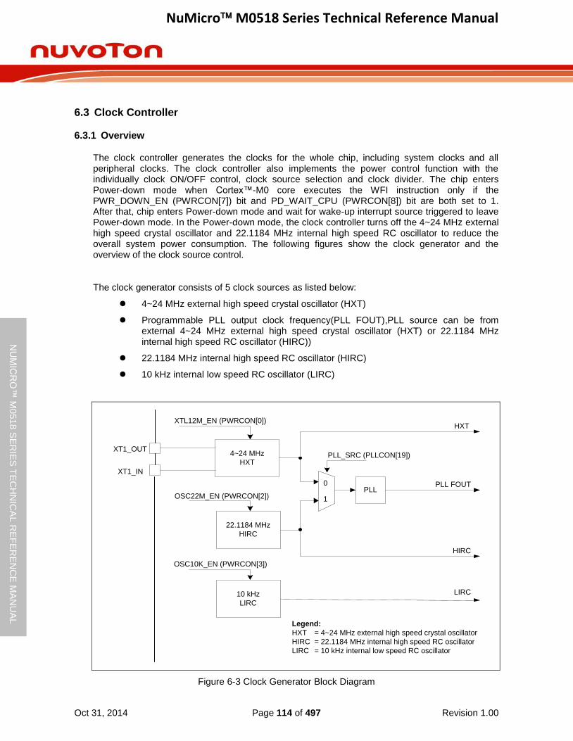
NuMicro M0518 Series Technical Reference Manual
Oct 31, 2014 Page 114 of 497 Revision 1.00
NU
MIC
RO
™ M
0518
SE
RIE
S T
EC
HN
ICA
L R
EF
ER
EN
CE
MA
NU
AL
6.3 Clock Controller
6.3.1 Overview
The clock controller generates the clocks for the whole chip, including system clocks and all peripheral clocks. The clock controller also implements the power control function with the individually clock ON/OFF control, clock source selection and clock divider. The chip enters Power-down mode when Cortex™-M0 core executes the WFI instruction only if the PWR_DOWN_EN (PWRCON[7]) bit and PD_WAIT_CPU (PWRCON[8]) bit are both set to 1. After that, chip enters Power-down mode and wait for wake-up interrupt source triggered to leave Power-down mode. In the Power-down mode, the clock controller turns off the 4~24 MHz external high speed crystal oscillator and 22.1184 MHz internal high speed RC oscillator to reduce the overall system power consumption. The following figures show the clock generator and the overview of the clock source control.
The clock generator consists of 5 clock sources as listed below:
4~24 MHz external high speed crystal oscillator (HXT)
Programmable PLL output clock frequency(PLL FOUT),PLL source can be from external 4~24 MHz external high speed crystal oscillator (HXT) or 22.1184 MHz internal high speed RC oscillator (HIRC))
22.1184 MHz internal high speed RC oscillator (HIRC)
10 kHz internal low speed RC oscillator (LIRC)
XT1_IN
4~24 MHz
HXT
XTL12M_EN (PWRCON[0])
XT1_OUT
22.1184 MHz
HIRC
OSC22M_EN (PWRCON[2])
0
1
PLL
PLL_SRC (PLLCON[19])
PLL FOUT
10 kHz
LIRC
OSC10K_EN (PWRCON[3])
HXT
HIRC
LIRC
Legend:
HXT = 4~24 MHz external high speed crystal oscillator
HIRC = 22.1184 MHz internal high speed RC oscillator
LIRC = 10 kHz internal low speed RC oscillator
Figure 6-3 Clock Generator Block Diagram
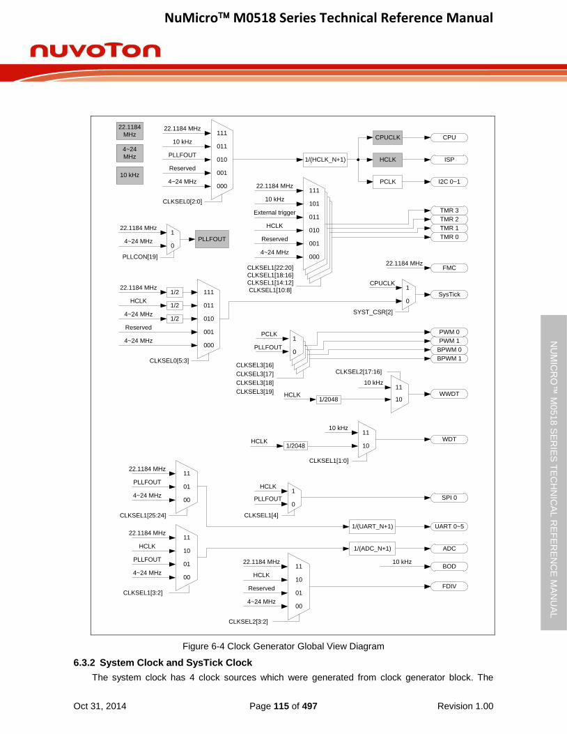
NuMicro M0518 Series Technical Reference Manual
Oct 31, 2014 Page 115 of 497 Revision 1.00
NU
MIC
RO
™ M
0518
SE
RIE
S T
EC
HN
ICA
L R
EF
ER
EN
CE
MA
NU
AL
1
0
PLLCON[19]
22.1184
MHz
4~24
MHz
PLLFOUT
111
011
010
001
4~24 MHz
Reserved
4~24 MHz
HCLK
22.1184 MHz
000
1/2
1/2
1/2
CLKSEL0[5:3]
1
0SysTick
TMR 0
ADC
UART 0~5
ISP
WDT
BPWM 0
TMR 3
TMR 2
TMR 1
CPU
FMC
10 kHz
011
010
001
000
HCLK
Reserved
4~24 MHz
111
011
010
001
PLLFOUT
Reserved
4~24 MHz
10 kHz
22.1184 MHz
000
CLKSEL0[2:0]
SYST_CSR[2]
CPUCLK
1/(HCLK_N+1)
PCLK
CPUCLK
HCLK
11
01
00
PLLFOUT
4~24 MHz
HCLK
CLKSEL1[3:2]
External trigger
CLKSEL1[22:20]
CLKSEL1[18:16]
CLKSEL1[14:12]
CLKSEL1[10:8]
22.1184 MHz
WWDT
10 kHz
1/(ADC_N+1)
11
10
CLKSEL1[1:0]
HCLK1/2048
1/(UART_N+1)
22.1184 MHz
4~24 MHz
11
01
00
PLLFOUT
4~24 MHz
22.1184 MHz
CLKSEL1[25:24]
22.1184 MHz
10
10 kHz
22.1184 MHz
101
111
1
0SPI 0
CLKSEL1[4]
HCLK
11
10
01
00
HCLK
4~24 MHz
22.1184 MHz
Reserved
CLKSEL2[3:2]
FDIV
BOD10 kHz
11
10
CLKSEL2[17:16]
10 kHz
CLKSEL3[17]
CLKSEL3[18]
I2C 0~1
PLLFOUT
PWM 01
0
PCLK
PLLFOUT
BPWM 1
PWM 1
CLKSEL3[16]
CLKSEL3[19]HCLK
1/2048
Figure 6-4 Clock Generator Global View Diagram
6.3.2 System Clock and SysTick Clock
The system clock has 4 clock sources which were generated from clock generator block. The

NuMicro M0518 Series Technical Reference Manual
Oct 31, 2014 Page 116 of 497 Revision 1.00
NU
MIC
RO
™ M
0518
SE
RIE
S T
EC
HN
ICA
L R
EF
ER
EN
CE
MA
NU
AL
clock source switch depends on the register HCLK_S (CLKSEL0[2:0]). The block diagram is shown in Figure 6-5.
111
011
010
001
PLLFOUT
Reserved
4~24 MHz
10 kHz
HCLK_S (CLKSEL0[2:0])
22.1184 MHz
000
1/(HCLK_N+1)
HCLK_N (CLKDIV[3:0])
CPU in Power Down Mode
CPU
AHB
APB
CPUCLK
HCLK
PCLK
Figure 6-5 System Clock Block Diagram
The clock source of SysTick in Cortex™-M0 core can use CPU clock or external clock (SYST_CSR[2]). If using external clock, the SysTick clock (STCLK) has 4 clock sources. The clock source switch depends on the setting of the register STCLK_S (CLKSEL0[5:3]). The block diagram is shown in Figure 6-6.
111
011
010
001
4~24 MHz
Reserved
4~24 MHz
HCLK
STCLK_S (CLKSEL0[5:3])
STCLK
22.1184 MHz
000
1/2
1/2
1/2
Figure 6-6 SysTick Clock Control Block Diagram

NuMicro M0518 Series Technical Reference Manual
Oct 31, 2014 Page 117 of 497 Revision 1.00
NU
MIC
RO
™ M
0518
SE
RIE
S T
EC
HN
ICA
L R
EF
ER
EN
CE
MA
NU
AL
6.3.3 Power-down Mode Clock
When chip enters Power-down mode, system clocks, some clock sources, and some peripheral clocks will be disabled. Some clock sources and peripherals clocks are still active in Power-down mode.
The clocks still kept active are listed below:
Clock Generator
- 10 kHz internal low speed RC oscillator (LIRC) clock
WDT/Timer Peripherals Clock (when 10 kHz intertnal low speed RC oscillator (LIRC) is adopted as clock source)
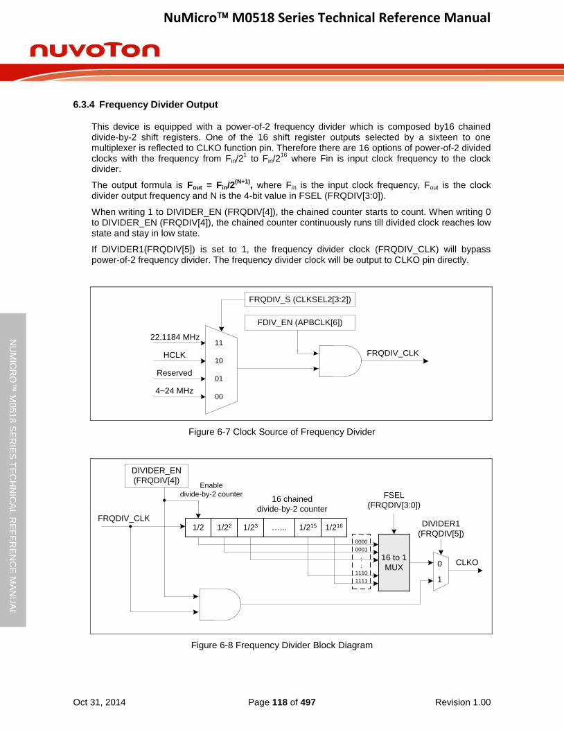
NuMicro M0518 Series Technical Reference Manual
Oct 31, 2014 Page 118 of 497 Revision 1.00
NU
MIC
RO
™ M
0518
SE
RIE
S T
EC
HN
ICA
L R
EF
ER
EN
CE
MA
NU
AL
6.3.4 Frequency Divider Output
This device is equipped with a power-of-2 frequency divider which is composed by16 chained divide-by-2 shift registers. One of the 16 shift register outputs selected by a sixteen to one multiplexer is reflected to CLKO function pin. Therefore there are 16 options of power-of-2 divided clocks with the frequency from Fin/2
1 to Fin/2
16 where Fin is input clock frequency to the clock
divider.
The output formula is Fout = Fin/2(N+1)
, where Fin is the input clock frequency, Fout is the clock divider output frequency and N is the 4-bit value in FSEL (FRQDIV[3:0]).
When writing 1 to DIVIDER_EN (FRQDIV[4]), the chained counter starts to count. When writing 0 to DIVIDER_EN (FRQDIV[4]), the chained counter continuously runs till divided clock reaches low state and stay in low state.
If DIVIDER1(FRQDIV[5]) is set to 1, the frequency divider clock (FRQDIV_CLK) will bypass power-of-2 frequency divider. The frequency divider clock will be output to CLKO pin directly.
11
10
01
00
HCLK
Reserved
4~24 MHz
22.1184 MHz
FRQDIV_S (CLKSEL2[3:2])
FDIV_EN (APBCLK[6])
FRQDIV_CLK
Figure 6-7 Clock Source of Frequency Divider
0000
0001
1110
1111
:
:
16 to 1
MUX
1/2 1/22 1/23 1/215 1/216…...
FSEL
(FRQDIV[3:0])
CLKO
FRQDIV_CLK
16 chained
divide-by-2 counter
DIVIDER_EN
(FRQDIV[4])Enable
divide-by-2 counter
0
1
DIVIDER1
(FRQDIV[5])
Figure 6-8 Frequency Divider Block Diagram
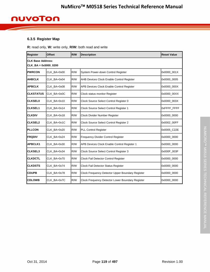
NuMicro M0518 Series Technical Reference Manual
Oct 31, 2014 Page 119 of 497 Revision 1.00
NU
MIC
RO
™ M
0518
SE
RIE
S T
EC
HN
ICA
L R
EF
ER
EN
CE
MA
NU
AL
6.3.5 Register Map
R: read only, W: write only, R/W: both read and write
Register Offset R/W Description Reset Value
CLK Base Address:
CLK_BA = 0x5000_0200
PWRCON CLK_BA+0x00 R/W System Power-down Control Register 0x0000_001X
AHBCLK CLK_BA+0x04 R/W AHB Devices Clock Enable Control Register 0x0000_0005
APBCLK CLK_BA+0x08 R/W APB Devices Clock Enable Control Register 0x0000_000X
CLKSTATUS CLK_BA+0x0C R/W Clock status monitor Register 0x0000_00XX
CLKSEL0 CLK_BA+0x10 R/W Clock Source Select Control Register 0 0x0000_003X
CLKSEL1 CLK_BA+0x14 R/W Clock Source Select Control Register 1 0xFFFF_FFFF
CLKDIV CLK_BA+0x18 R/W Clock Divider Number Register 0x0000_0000
CLKSEL2 CLK_BA+0x1C R/W Clock Source Select Control Register 2 0x0002_00FF
PLLCON CLK_BA+0x20 R/W PLL Control Register 0x0005_C22E
FRQDIV CLK_BA+0x24 R/W Frequency Divider Control Register 0x0000_0000
APBCLK1 CLK_BA+0x30 R/W APB Devices Clock Enable Control Register 1 0x0000_0000
CLKSEL3 CLK_BA+0x34 R/W Clock Source Select Control Register 3 0x000F_003F
CLKDCTL CLK_BA+0x70 R/W Clock Fail Detector Control Register 0x0000_0000
CLKDSTS CLK_BA+0x74 R/W Clock Fail Detector Status Register 0x0000_0000
CDUPB CLK_BA+0x78 R/W Clock Frequency Detector Upper Boundary Register 0x0000_0000
CDLOWB CLK_BA+0x7C R/W Clock Frequency Detector Lower Boundary Register 0x0000_0000

NuMicro M0518 Series Technical Reference Manual
Oct 31, 2014 Page 120 of 497 Revision 1.00
NU
MIC
RO
™ M
0518
SE
RIE
S T
EC
HN
ICA
L R
EF
ER
EN
CE
MA
NU
AL
6.3.6 Register Description
System Power-down Control Register (PWRCON)
Except the BIT[6], all the other bits are protected, programming these bits need to write “59h”, “16h”, “88h” to address 0x5000_0100 to disable register protection. Refer to the register REGWRPROT at address GCR_BA+0x100
Register Offset R/W Description Reset Value
PWRCON CLK_BA+0x00 R/W System Power-down Control Register 0x0000_001X
31 30 29 28 27 26 25 24
Reserved
23 22 21 20 19 18 17 16
Reserved
15 14 13 12 11 10 9 8
Reserved PD_WAIT_
CPU
7 6 5 4 3 2 1 0
PWR_DOWN_EN
PD_WU_STS PD_WU_INT_
EN PD_WU_DLY OSC10K_EN OSC22M_EN Reserved XTL12M_EN
Bits Description
[31:18] Reserved Reserved.
[15:9] Reserved Reserved.
[8] PD_WAIT_CPU
Power-Down Entry Condition Control (Write Protect)
0 = Chip enters Power-down mode when the PWR_DOWN_EN bit is set to 1.
1 = Chip enters Power- down mode when the both PD_WAIT_CPU and PWR_DOWN_EN bits are set to 1 and CPU runs WFI instruction.
Note: This bit is the protected bit, and programming it needs to write “59h”, “16h”, and “88h” to address 0x5000_0100 to disable register protection. Refer to the register REGWRPROT at address GCR_BA+0x100.
[7] PWR_DOWN_EN
System Power-Down Enable Bit (Write Protect)
When this bit is set to 1, Power-down mode is enabled and chip Power-down behavior will depends on the PD_WAIT_CPU bit
(a) If the PD_WAIT_CPU is 0, the chip enters Power-down mode immediately after the PWR_DOWN_EN bit set.
(b) if the PD_WAIT_CPU is 1, the chip keeps active till the CPU sleep mode is also active and then the chip enters Power-down mode (recommend)
When chip wakes up from Power-down mode, this bit is cleared by hardware. User needs to set this bit again for next Power-down.
In Power-down mode, 4~24 MHz external high speed crystal oscillator (HXT) and the 22.1184 MHz internal high speed RC oscillator (HIRC) will be disabled in this mode, but the 10 kHz internal low speed RC oscillator (LIRC) is not controlled by Power-down mode.
In Power- down mode, the PLL and system clock are disabled, and ignored the clock source selection. The clocks of peripheral are not controlled by Power-down mode, if the

NuMicro M0518 Series Technical Reference Manual
Oct 31, 2014 Page 121 of 497 Revision 1.00
NU
MIC
RO
™ M
0518
SE
RIE
S T
EC
HN
ICA
L R
EF
ER
EN
CE
MA
NU
AL
peripheral clock source is from the 10 kHz internal low speed RC oscillator (LIRC).
0 = Chip operating normally or chip in Idle mode because of WFI command.
1 = Chip enters Power-down mode instantly or waits CPU sleep command WFI.
Note: This bit is the protected bit, and programming it needs to write “59h”, “16h”, and “88h” to address 0x5000_0100 to disable register protection. Refer to the register REGWRPROT at address GCR_BA+0x100.
[6] PD_WU_STS
Power-Down Mode Wake-Up Interrupt Status
Set by “Power-down wake-up event”, it indicates that resume from Power-down mode”.
The flag is set if the GPIO, UART, WDT, I2C, TIMER, or BOD wake-up occurred.
Write 1 to clear the bit to 0.
Note: This bit is working only if PD_WU_INT_EN (PWRCON[5]) set to 1.
[5] PD_WU_INT_EN
Power-Down Mode Wake-Up Interrupt Enable Bit (Write Protect)
0 = Power-down mode wake-up interrupt Disabled.
1 = Power-down mode wake-up interrupt Enabled.
Note1: The interrupt will occur when both PD_WU_STS and PD_WU_INT_EN are high.
Note2: This bit is the protected bit, and programming it needs to write “59h”, “16h”, and “88h” to address 0x5000_0100 to disable register protection. Refer to the register REGWRPROT at address GCR_BA+0x100.
[4] PD_WU_DLY
Wake-Up Delay Counter Enable Bit (Write Protect)
When the chip wakes up from Power-down mode, the clock control will delay certain clock cycles to wait system clock stable.
The delayed clock cycle is 4096 clock cycles when chip works at 4~24 MHz external high speed crystal oscillator (HXT), and 256 clock cycles when chip works at 22.1184 MHz internal high speed oscillator (HIRC).
0 = Clock cycles delay Disabled.
1 = Clock cycles delay Enabled.
Note: This bit is the protected bit, and programming it needs to write “59h”, “16h”, and “88h” to address 0x5000_0100 to disable register protection. Refer to the register REGWRPROT at address GCR_BA+0x100.
[3] OSC10K_EN
10 KHz Internal Low Speed RC Oscillator (LIRC) Enable Bit (Write Protect)
0 = 10 kHz internal low speed RC oscillator (LIRC) Disabled.
1 = 10 kHz internal low speed RC oscillator (LIRC) Enabled.
Note: This bit is the protected bit, and programming it needs to write “59h”, “16h”, and “88h” to address 0x5000_0100 to disable register protection. Refer to the register REGWRPROT at address GCR_BA+0x100.
[2] OSC22M_EN
22.1184 MHz Internal High Speed RC Oscillator (HIRC) Enable Bit (Write Protect)
0 = 22.1184 MHz internal high speed RC oscillator (HIRC) Disabled.
1 = 22.1184 MHz internal high speed RC oscillator (HIRC) Enabled.
Note: This bit is the protected bit, and programming it needs to write “59h”, “16h”, and “88h” to address 0x5000_0100 to disable register protection. Refer to the register REGWRPROT at address GCR_BA+0x100.
[1] Reserved Reserved.
[0] XTL12M_EN
4~24 MHz External High Speed Crystal Oscillator (HXT) Enable Bit (Write Protect)
The bit default value is set by flash controller user configuration register CONFIG0 [26:24]. When the default clock source is from 4~24 MHz external high speed crystal oscillator, this bit is set to 1 automatically.
0 = 4 ~ 24 MHz external high speed crystal oscillator (HXT) Disabled.
1 = 4 ~ 24 MHz external high speed crystal oscillator (HXT) Enabled.
Note: This bit is the protected bit, and programming it needs to write “59h”, “16h”, and “88h” to address 0x5000_0100 to disable register protection. Refer to the register
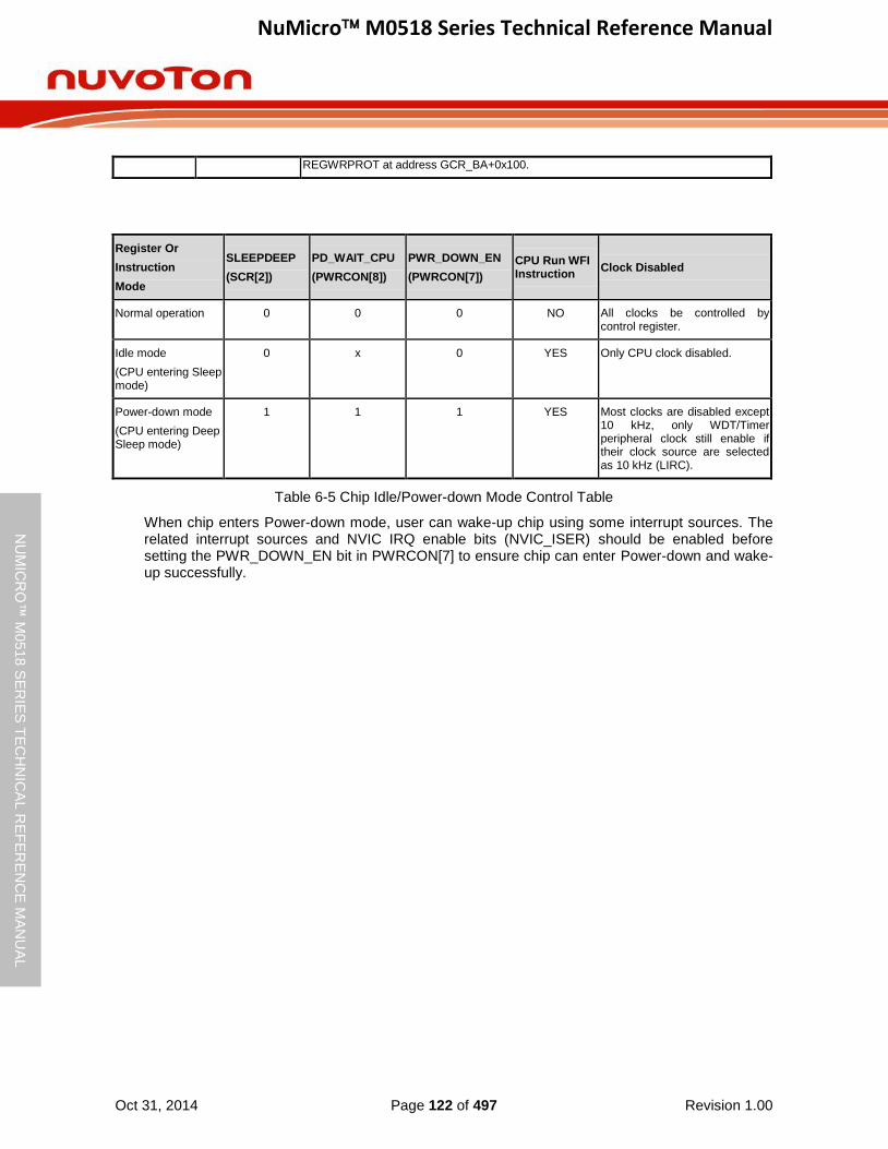
NuMicro M0518 Series Technical Reference Manual
Oct 31, 2014 Page 122 of 497 Revision 1.00
NU
MIC
RO
™ M
0518
SE
RIE
S T
EC
HN
ICA
L R
EF
ER
EN
CE
MA
NU
AL
REGWRPROT at address GCR_BA+0x100.
Register Or
Instruction
Mode
SLEEPDEEP
(SCR[2])
PD_WAIT_CPU
(PWRCON[8])
PWR_DOWN_EN
(PWRCON[7])
CPU Run WFI Instruction
Clock Disabled
Normal operation 0 0 0 NO All clocks be controlled by control register.
Idle mode
(CPU entering Sleep mode)
0 x 0 YES Only CPU clock disabled.
Power-down mode
(CPU entering Deep Sleep mode)
1 1 1 YES Most clocks are disabled except 10 kHz, only WDT/Timer peripheral clock still enable if their clock source are selected as 10 kHz (LIRC).
Table 6-5 Chip Idle/Power-down Mode Control Table
When chip enters Power-down mode, user can wake-up chip using some interrupt sources. The related interrupt sources and NVIC IRQ enable bits (NVIC_ISER) should be enabled before setting the PWR_DOWN_EN bit in PWRCON[7] to ensure chip can enter Power-down and wake-up successfully.

NuMicro M0518 Series Technical Reference Manual
Oct 31, 2014 Page 123 of 497 Revision 1.00
NU
MIC
RO
™ M
0518
SE
RIE
S T
EC
HN
ICA
L R
EF
ER
EN
CE
MA
NU
AL
AHB Devices Clock Enable Control Register (AHBCLK)
Register Offset R/W Description Reset Value
AHBCLK CLK_BA+0x04 R/W AHB Devices Clock Enable Control Register 0x0000_0005
31 30 29 28 27 26 25 24
Reserved
23 22 21 20 19 18 17 16
Reserved
15 14 13 12 11 10 9 8
Reserved
7 6 5 4 3 2 1 0
Reserved ISP_EN Reserved
Bits Description
[31:3] Reserved Reserved.
[2] ISP_EN
Flash ISP Controller Clock Enable Bit
0 = Flash ISP peripherial clock Disabled.
1 = Flash ISP peripherial clock Enabled.
[1:0] Reserved Reserved.
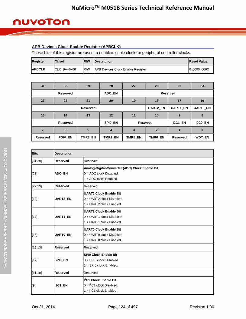
NuMicro M0518 Series Technical Reference Manual
Oct 31, 2014 Page 124 of 497 Revision 1.00
NU
MIC
RO
™ M
0518
SE
RIE
S T
EC
HN
ICA
L R
EF
ER
EN
CE
MA
NU
AL
APB Devices Clock Enable Register (APBCLK)
These bits of this register are used to enable/disable clock for peripheral controller clocks.
Register Offset R/W Description Reset Value
APBCLK CLK_BA+0x08 R/W APB Devices Clock Enable Register 0x0000_000X
31 30 29 28 27 26 25 24
Reserved ADC_EN Reserved
23 22 21 20 19 18 17 16
Reserved UART2_EN UART1_EN UART0_EN
15 14 13 12 11 10 9 8
Reserved SPI0_EN Reserved I2C1_EN I2C0_EN
7 6 5 4 3 2 1 0
Reserved FDIV_EN TMR3_EN TMR2_EN TMR1_EN TMR0_EN Reserved WDT_EN
Bits Description
[31:29] Reserved Reserved.
[28] ADC_EN
Analog-Digital-Converter (ADC) Clock Enable Bit
0 = ADC clock Disabled.
1 = ADC clock Enabled.
[27:19] Reserved Reserved.
[18] UART2_EN
UART2 Clock Enable Bit
0 = UART2 clock Disabled.
1 = UART2 clock Enabled.
[17] UART1_EN
UART1 Clock Enable Bit
0 = UART1 clock Disabled.
1 = UART1 clock Enabled.
[16] UART0_EN
UART0 Clock Enable Bit
0 = UART0 clock Disabled.
1 = UART0 clock Enabled.
[15:13] Reserved Reserved.
[12] SPI0_EN
SPI0 Clock Enable Bit
0 = SPI0 clock Disabled.
1 = SPI0 clock Enabled.
[11:10] Reserved Reserved.
[9] I2C1_EN
I2C1 Clock Enable Bit
0 = I2C1 clock Disabled.
1 = I2C1 clock Enabled.

NuMicro M0518 Series Technical Reference Manual
Oct 31, 2014 Page 125 of 497 Revision 1.00
NU
MIC
RO
™ M
0518
SE
RIE
S T
EC
HN
ICA
L R
EF
ER
EN
CE
MA
NU
AL
[8] I2C0_EN
I2C0 Clock Enable Bit
0 = I2C0 clock Disabled.
1 = I2C0 clock Enabled.
[7] Reserved Reserved.
[6] FDIV_EN
Frequency Divider Output Clock Enable Bit
0 = FDIV clock Disabled.
1 = FDIV clock Enabled.
[5] TMR3_EN
Timer3 Clock Enable Bit
0 = Timer3 clock Disabled.
1 = Timer3 clock Enabled.
[4] TMR2_EN
Timer2 Clock Enable Bit
0 = Timer2 clock Disabled.
1 = Timer2 clock Enabled.
[3] TMR1_EN
Timer1 Clock Enable Bit
0 = Timer1 clock Disabled.
1 = Timer1 clock Enabled.
[2] TMR0_EN
Timer0 Clock Enable Bit
0 = Timer0 clock Disabled.
1 = Timer0 clock Enabled.
[1] Reserved Reserved.
[0] WDT_EN
Watchdog Timer Clock Enable Bit (Write Protect)
0 = Watchdog Timer clock Disabled.
1 = Watchdog Timer clock Enabled.
Note: This bit is the protected bit, and programming it needs to write “59h”, “16h”, and “88h” to address 0x5000_0100 to disable register protection. Refer to the register REGWRPROT at address GCR_BA+0x100.

NuMicro M0518 Series Technical Reference Manual
Oct 31, 2014 Page 126 of 497 Revision 1.00
NU
MIC
RO
™ M
0518
SE
RIE
S T
EC
HN
ICA
L R
EF
ER
EN
CE
MA
NU
AL
Clock status Register (CLKSTATUS)
These bits of this register are used to monitor if the chip clock source stable or not, and whether clock switch failed.
Register Offset R/W Description Reset Value
CLKSTATUS CLK_BA+0x0C R/W Clock status monitor Register 0x0000_00XX
31 30 29 28 27 26 25 24
Reserved
23 22 21 20 19 18 17 16
Reserved
15 14 13 12 11 10 9 8
Reserved
7 6 5 4 3 2 1 0
CLK_SW_
FAIL Reserved
OSC22M_
STB
OSC10K_
STB PLL_STB Reserved XTL12M_STB
Bits Description
[31:8] Reserved Reserved.
[7] CLK_SW_FAIL
Clock Switching Fail Flag (Read Only)
0 = Clock switching success.
1 = Clock switching failure.
This bit is an index that if current system clock source is match as user defined at HCLK_S (CLKSEL[2:0]). When user switchs system clock, the system clock source will keep old clock until the new clock is stable. During the period that waiting new clock stable, this bit will be an index shows system clock source is not match as user wanted.
[6:5] Reserved Reserved.
[4] OSC22M_STB
22.1184 MHz Internal High Speed RC Oscillator (HIRC) Clock Source Stable Flag (Read Only)
0 = 22.1184 MHz internal high speed RC oscillator (HIRC) clock is not stable or disabled.
1 = 22.1184 MHz internal high speed RC oscillator (HIRC) clock is stable and enabled.
[3] OSC10K_STB
Internal 10 KHz Low Speed Oscillator (LIRC) Clock Source Stable Flag (Read Only)
0 = 10 kHz internal low speed RC oscillator (LIRC) clock is not stable or disabled.
1 = 10 kHz internal low speed RC oscillator (LIRC) clock is stable and enabled.
[2] PLL_STB
Internal PLL Clock Source Stable Flag (Read Only)
0 = Internal PLL clock is not stable or disabled.
1 = Internal PLL clock is stable in normal mode.
[1] Reserved Reserved.
[0] XTL12M_STB
4~24 MHz External High Speed Crystal Oscillator (HXT) Clock Source Stable Flag (Read Only)
0 = 4~24 MHz external high speed crystal oscillator (HXT) clock is not stable or disabled.

NuMicro M0518 Series Technical Reference Manual
Oct 31, 2014 Page 127 of 497 Revision 1.00
NU
MIC
RO
™ M
0518
SE
RIE
S T
EC
HN
ICA
L R
EF
ER
EN
CE
MA
NU
AL
1 = 4~24 MHz external high speed crystal oscillator (HXT) clock is stable and enabled.
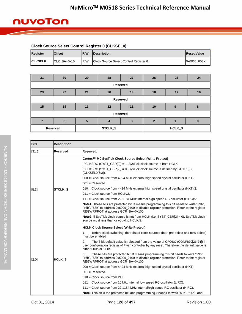
NuMicro M0518 Series Technical Reference Manual
Oct 31, 2014 Page 128 of 497 Revision 1.00
NU
MIC
RO
™ M
0518
SE
RIE
S T
EC
HN
ICA
L R
EF
ER
EN
CE
MA
NU
AL
Clock Source Select Control Register 0 (CLKSEL0)
Register Offset R/W Description Reset Value
CLKSEL0 CLK_BA+0x10 R/W Clock Source Select Control Register 0 0x0000_003X
31 30 29 28 27 26 25 24
Reserved
23 22 21 20 19 18 17 16
Reserved
15 14 13 12 11 10 9 8
Reserved
7 6 5 4 3 2 1 0
Reserved STCLK_S HCLK_S
Bits Description
[31:6] Reserved Reserved.
[5:3] STCLK_S
Cortex™-M0 SysTick Clock Source Select (Write Protect)
If CLKSRC (SYST_CSR[2]) = 1, SysTick clock source is from HCLK.
If CLKSRC (SYST_CSR[2]) = 0, SysTick clock source is defined by STCLK_S (CLKSEL0[5:3]).
000 = Clock source from 4~24 MHz external high speed crystal oscillator (HXT).
001 = Reserved.
010 = Clock source from 4~24 MHz external high speed crystal oscillator (HXT)/2.
011 = Clock source from HCLK/2.
111 = Clock source from 22.1184 MHz internal high speed RC oscillator (HIRC)/2.
Note1: These bits are protected bit. It means programming this bit needs to write “59h”, “16h”, “88h” to address 0x5000_0100 to disable register protection. Refer to the register REGWRPROT at address GCR_BA+0x100.
Note2: if SysTick clock source is not from HCLK (i.e. SYST_CSR[2] = 0), SysTick clock source must less than or equal to HCLK/2.
[2:0] HCLK_S
HCLK Clock Source Select (Write Protect)
1. Before clock switching, the related clock sources (both pre-select and new-select) must be enabled
2. The 3-bit default value is reloaded from the value of CFOSC (CONFIG0[26:24]) in user configuration register of Flash controller by any reset. Therefore the default value is either 000b or 111b.
3. These bits are protected bit. It means programming this bit needs to write “59h”, “16h”, “88h” to address 0x5000_0100 to disable register protection. Refer to the register REGWRPROT at address GCR_BA+0x100.
000 = Clock source from 4~24 MHz external high speed crystal oscillator (HXT).
001 = Reserved.
010 = Clock source from PLL.
011 = Clock source from 10 kHz internal low speed RC oscillator (LIRC).
111 = Clock source from 22.1184 MHz internalhigh speed RC oscillator (HIRC).
Note: This bit is the protected bit, and programming it needs to write “59h”, “16h”, and

NuMicro M0518 Series Technical Reference Manual
Oct 31, 2014 Page 129 of 497 Revision 1.00
NU
MIC
RO
™ M
0518
SE
RIE
S T
EC
HN
ICA
L R
EF
ER
EN
CE
MA
NU
AL
“88h” to address 0x5000_0100 to disable register protection. Refer to the register REGWRPROT at address GCR_BA+0x100.
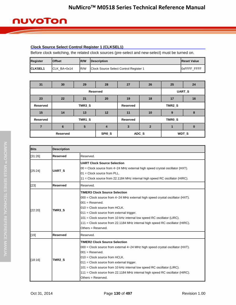
NuMicro M0518 Series Technical Reference Manual
Oct 31, 2014 Page 130 of 497 Revision 1.00
NU
MIC
RO
™ M
0518
SE
RIE
S T
EC
HN
ICA
L R
EF
ER
EN
CE
MA
NU
AL
Clock Source Select Control Register 1 (CLKSEL1)
Before clock switching, the related clock sources (pre-select and new-select) must be turned on.
Register Offset R/W Description Reset Value
CLKSEL1 CLK_BA+0x14 R/W Clock Source Select Control Register 1 0xFFFF_FFFF
31 30 29 28 27 26 25 24
Reserved UART_S
23 22 21 20 19 18 17 16
Reserved TMR3_S Reserved TMR2_S
15 14 13 12 11 10 9 8
Reserved TMR1_S Reserved TMR0_S
7 6 5 4 3 2 1 0
Reserved SPI0_S ADC_S WDT_S
Bits Description
[31:26] Reserved Reserved.
[25:24] UART_S
UART Clock Source Selection
00 = Clock source from 4~24 MHz external high speed crystal oscillator (HXT).
01 = Clock source from PLL.
11 = Clock source from 22.1184 MHz internal high speed RC oscillator (HIRC).
[23] Reserved Reserved.
[22:20] TMR3_S
TIMER3 Clock Source Selection
000 = Clock source from 4~24 MHz external high speed crystal oscillator (HXT).
001 = Reserved.
010 = Clock source from HCLK.
011 = Clock source from external trigger.
101 = Clock source from 10 kHz internal low speed RC oscillator (LIRC).
111 = Clock source from 22.1184 MHz internal high speed RC oscillator (HIRC).
Others = Reserved.
[19] Reserved Reserved.
[18:16] TMR2_S
TIMER2 Clock Source Selection
000 = Clock source from external 4~24 MHz high speed crystal oscillator (HXT).
001 = Reserved.
010 = Clock source from HCLK.
011 = Clock source from external trigger.
101 = Clock source from 10 kHz internal low speed RC oscillator (LIRC).
111 = Clock source from 22.1184 MHz internal high speed RC oscillator (HIRC).
Others = Reserved.
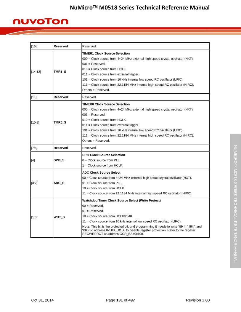
NuMicro M0518 Series Technical Reference Manual
Oct 31, 2014 Page 131 of 497 Revision 1.00
NU
MIC
RO
™ M
0518
SE
RIE
S T
EC
HN
ICA
L R
EF
ER
EN
CE
MA
NU
AL
[15] Reserved Reserved.
[14:12] TMR1_S
TIMER1 Clock Source Selection
000 = Clock source from 4~24 MHz external high speed crystal oscillator (HXT).
001 = Reserved.
010 = Clock source from HCLK.
011 = Clock source from external trigger.
101 = Clock source from 10 kHz internal low speed RC oscillator (LIRC).
111 = Clock source from 22.1184 MHz internal high speed RC oscillator (HIRC).
Others = Reserved.
[11] Reserved Reserved.
[10:8] TMR0_S
TIMER0 Clock Source Selection
000 = Clock source from 4~24 MHz external high speed crystal oscillator (HXT).
001 = Reserved.
010 = Clock source from HCLK.
011 = Clock source from external trigger.
101 = Clock source from 10 kHz internal low speed RC oscillator (LIRC).
111 = Clock source from 22.1184 MHz internal high speed RC oscillator (HIRC).
Others = Reserved.
[7:5] Reserved Reserved.
[4] SPI0_S
SPI0 Clock Source Selection
0 = Clock source from PLL.
1 = Clock source from HCLK.
[3:2] ADC_S
ADC Clock Source Select
00 = Clock source from 4~24 MHz external high speed crystal oscillator (HXT).
01 = Clock source from PLL.
10 = Clock source from HCLK.
11 = Clock source from 22.1184 MHz internal high speed RC oscillator (HIRC).
[1:0] WDT_S
Watchdog Timer Clock Source Select (Write Protect)
00 = Reserved.
01 = Reserved.
10 = Clock source from HCLK/2048.
11 = Clock source from 10 kHz internal low speed RC oscillator (LIRC).
Note: This bit is the protected bit, and programming it needs to write “59h”, “16h”, and “88h” to address 0x5000_0100 to disable register protection. Refer to the register REGWRPROT at address GCR_BA+0x100.
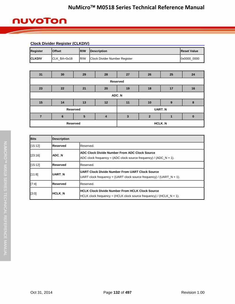
NuMicro M0518 Series Technical Reference Manual
Oct 31, 2014 Page 132 of 497 Revision 1.00
NU
MIC
RO
™ M
0518
SE
RIE
S T
EC
HN
ICA
L R
EF
ER
EN
CE
MA
NU
AL
Clock Divider Register (CLKDIV)
Register Offset R/W Description Reset Value
CLKDIV CLK_BA+0x18 R/W Clock Divider Number Register 0x0000_0000
31 30 29 28 27 26 25 24
Reserved
23 22 21 20 19 18 17 16
ADC_N
15 14 13 12 11 10 9 8
Reserved UART_N
7 6 5 4 3 2 1 0
Reserved HCLK_N
Bits Description
[15:12] Reserved Reserved.
[23:16] ADC_N ADC Clock Divide Number From ADC Clock Source
ADC clock frequency = (ADC clock source frequency) / (ADC_N + 1).
[15:12] Reserved Reserved.
[11:8] UART_N UART Clock Divide Number From UART Clock Source
UART clock frequency = (UART clock source frequency) / (UART_N + 1).
[7:4] Reserved Reserved.
[3:0] HCLK_N HCLK Clock Divide Number From HCLK Clock Source
HCLK clock frequency = (HCLK clock source frequency) / (HCLK_N + 1).

NuMicro M0518 Series Technical Reference Manual
Oct 31, 2014 Page 133 of 497 Revision 1.00
NU
MIC
RO
™ M
0518
SE
RIE
S T
EC
HN
ICA
L R
EF
ER
EN
CE
MA
NU
AL
Clock Source Select Control Register 2 (CLKSEL2)
Before clock switching, the related clock sources (pre-select and new-select) must be turned on.
Register Offset R/W Description Reset Value
CLKSEL2 CLK_BA+0x1C R/W Clock Source Select Control Register 2 0x0002_00FF
31 30 29 28 27 26 25 24
Reserved
23 22 21 20 19 18 17 16
Reserved WWDT_S
15 14 13 12 11 10 9 8
Reserved
7 6 5 4 3 2 1 0
Reserved FRQDIV_S Reserved
Bits Description
[31:18] Reserved Reserved.
[17:16] WWDT_S
Window Watchdog Timer Clock Source Selection
10 = Clock source from HCLK/2048 clock.
11 = Clock source from 10 kHz internal low speed RC oscillator clock.
[15:4] Reserved Reserved.
[3:2] FRQDIV_S
Clock Divider Clock Source Selection
00 = Clock source from 4~24 MHz external high speed crystal oscillator clock.
01 = Reserved.
10 = Clock source from HCLK.
11 = Clock source from 22.1184 MHz internal high speed RC oscillator clock.
[1:0] Reserved Reserved.
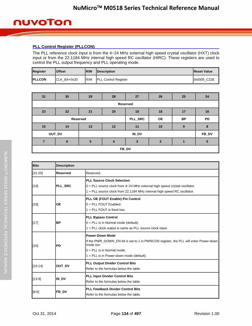
NuMicro M0518 Series Technical Reference Manual
Oct 31, 2014 Page 134 of 497 Revision 1.00
NU
MIC
RO
™ M
0518
SE
RIE
S T
EC
HN
ICA
L R
EF
ER
EN
CE
MA
NU
AL
PLL Control Register (PLLCON)
The PLL reference clock input is from the 4~24 MHz external high speed crystal oscillator (HXT) clock input or from the 22.1184 MHz internal high speed RC oscillator (HIRC). These registers are used to control the PLL output frequency and PLL operating mode.
Register Offset R/W Description Reset Value
PLLCON CLK_BA+0x20 R/W PLL Control Register 0x0005_C22E
31 30 29 28 27 26 25 24
Reserved
23 22 21 20 19 18 17 16
Reserved PLL_SRC OE BP PD
15 14 13 12 11 10 9 8
OUT_DV IN_DV FB_DV
7 6 5 4 3 2 1 0
FB_DV
Bits Description
[31:20] Reserved Reserved.
[19] PLL_SRC
PLL Source Clock Selection
0 = PLL source clock from 4~24 MHz external high speed crystal oscillator.
1 = PLL source clock from 22.1184 MHz internal high speed RC oscillator.
[18] OE
PLL OE (FOUT Enable) Pin Control
0 = PLL FOUT Enabled.
1 = PLL FOUT is fixed low.
[17] BP
PLL Bypass Control
0 = PLL is in Normal mode (default).
1 = PLL clock output is same as PLL source clock input.
[16] PD
Power-Down Mode
If the PWR_DOWN_EN bit is set to 1 in PWRCON register, the PLL will enter Power-down mode too.
0 = PLL is in Normal mode.
1 = PLL is in Power-down mode (default).
[15:14] OUT_DV PLL Output Divider Control Bits
Refer to the formulas below the table.
[13:9] IN_DV PLL Input Divider Control Bits
Refer to the formulas below the table.
[8:0] FB_DV PLL Feedback Divider Control Bits
Refer to the formulas below the table.
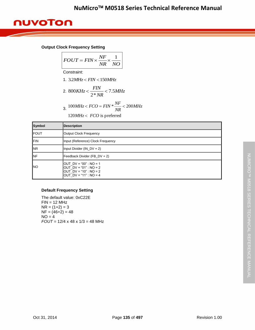
NuMicro M0518 Series Technical Reference Manual
Oct 31, 2014 Page 135 of 497 Revision 1.00
NU
MIC
RO
™ M
0518
SE
RIE
S T
EC
HN
ICA
L R
EF
ER
EN
CE
MA
NU
AL
Output Clock Frequency Setting
NONR
NFFINFOUT
1
Constraint:
1. MHzFINMHz. 15023
2. MHzNR
FINKHz 5.7
*2800
3.
preferred is120
200*100
FCO MHz
MHzNR
NFFINFCOMHz
Symbol Description
FOUT Output Clock Frequency
FIN Input (Reference) Clock Frequency
NR Input Divider (IN_DV + 2)
NF Feedback Divider (FB_DV + 2)
NO
OUT_DV = “00” : NO = 1 OUT_DV = “01” : NO = 2 OUT_DV = “10” : NO = 2 OUT_DV = “11” : NO = 4
Default Frequency Setting
The default value: 0xC22E FIN = 12 MHz NR = (1+2) = 3 NF = (46+2) = 48 NO = 4 FOUT = 12/4 x 48 x 1/3 = 48 MHz
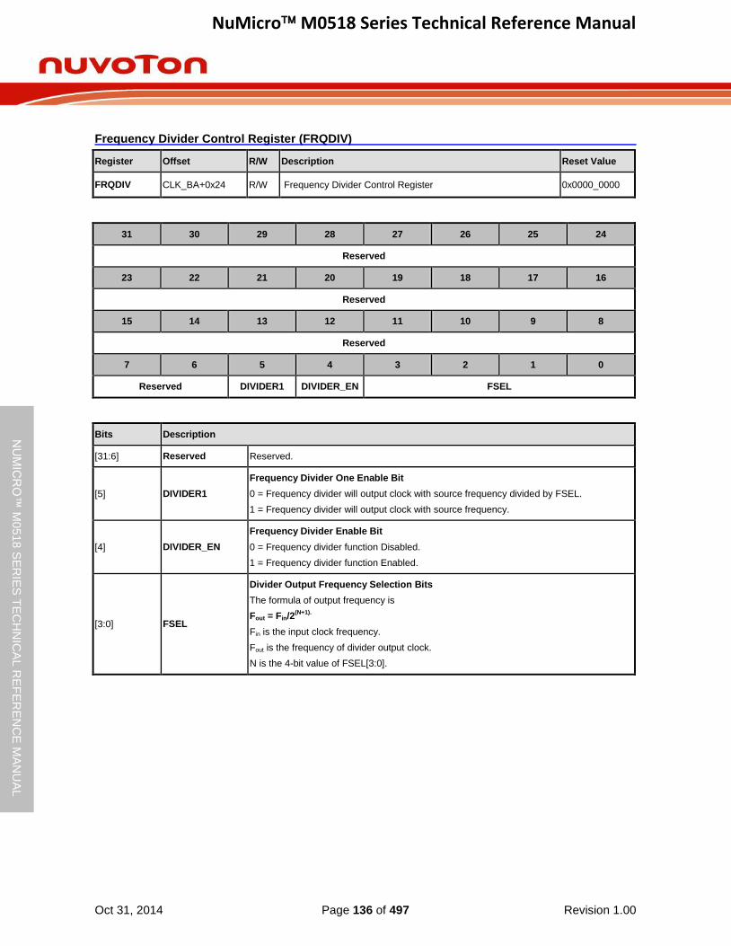
NuMicro M0518 Series Technical Reference Manual
Oct 31, 2014 Page 136 of 497 Revision 1.00
NU
MIC
RO
™ M
0518
SE
RIE
S T
EC
HN
ICA
L R
EF
ER
EN
CE
MA
NU
AL
Frequency Divider Control Register (FRQDIV)
Register Offset R/W Description Reset Value
FRQDIV CLK_BA+0x24 R/W Frequency Divider Control Register 0x0000_0000
31 30 29 28 27 26 25 24
Reserved
23 22 21 20 19 18 17 16
Reserved
15 14 13 12 11 10 9 8
Reserved
7 6 5 4 3 2 1 0
Reserved DIVIDER1 DIVIDER_EN FSEL
Bits Description
[31:6] Reserved Reserved.
[5] DIVIDER1
Frequency Divider One Enable Bit
0 = Frequency divider will output clock with source frequency divided by FSEL.
1 = Frequency divider will output clock with source frequency.
[4] DIVIDER_EN
Frequency Divider Enable Bit
0 = Frequency divider function Disabled.
1 = Frequency divider function Enabled.
[3:0] FSEL
Divider Output Frequency Selection Bits
The formula of output frequency is
Fout = Fin/2(N+1).
Fin is the input clock frequency.
Fout is the frequency of divider output clock.
N is the 4-bit value of FSEL[3:0].

NuMicro M0518 Series Technical Reference Manual
Oct 31, 2014 Page 137 of 497 Revision 1.00
NU
MIC
RO
™ M
0518
SE
RIE
S T
EC
HN
ICA
L R
EF
ER
EN
CE
MA
NU
AL
APB Devices Clock Enable Register 1 (APBCLK1)
These bits of this register are used to enable/disable clock for peripheral controller clocks.
Register Offset R/W Description Reset Value
APBCLK1 CLK_BA+0x30 R/W APB Devices Clock Enable Register 1 0x0000_0000
31 30 29 28 27 26 25 24
Reserved
23 22 21 20 19 18 17 16
Reserved BPWM1_EN BPWM0_EN PWM1_EN PWM0_EN
15 14 13 12 11 10 9 8
Reserved UART5_EN UART4_EN UART3_EN
7 6 5 4 3 2 1 0
Reserved
Bits Description
[31:20] Reserved Reserved.
[19] BPWM1_EN
BPWM1 Clock Enable Bit
0 = BPWM1 clock Disabled.
1 = BPWM1 clock Enabled.
[18] BPWM0_EN
BPWM0 Clock Enable Bit
0 = BPWM0 clock Disabled.
1 = BPWM0 clock Enabled.
[17] PWM1_EN
PWM1 Clock Enable Bit
0 = PWM1 clock Disabled.
1 = PWM1 clock Enabled.
[16] PWM0_EN
PWM0 Clock Enable Bit
0 = PWM0 clock Disabled.
1 = PWM0 clock Enabled.
[15:11] Reserved Reserved.
[10] UART5_EN
UART5 Clock Enable Bit
0 = UART5 clock Disabled.
1 = UART5 clock Enabled.
[9] UART4_EN
UART4 Clock Enable Bit
0 = UART4 clock Disabled.
1 = UART4 clock Enabled.
[8] UART3_EN
UART3 Clock Enable Bit
0 = UART3 clock Disabled.
1 = UART3 clock Enabled.
NuMicro M0518 Series Technical Reference Manual
Oct 31, 2014 Page 138 of 497 Revision 1.00
NU
MIC
RO
™ M
0518
SE
RIE
S T
EC
HN
ICA
L R
EF
ER
EN
CE
MA
NU
AL
[7:0] Reserved Reserved.
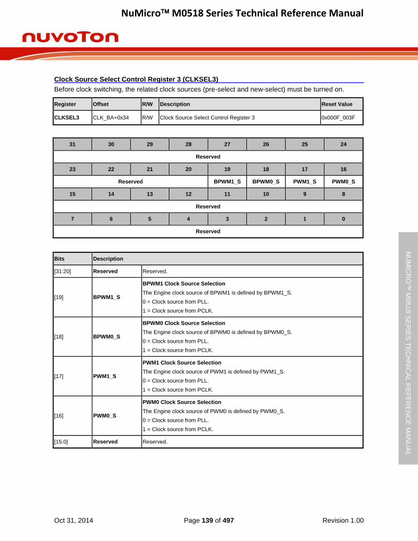
NuMicro M0518 Series Technical Reference Manual
Oct 31, 2014 Page 139 of 497 Revision 1.00
NU
MIC
RO
™ M
0518
SE
RIE
S T
EC
HN
ICA
L R
EF
ER
EN
CE
MA
NU
AL
Clock Source Select Control Register 3 (CLKSEL3)
Before clock switching, the related clock sources (pre-select and new-select) must be turned on.
Register Offset R/W Description Reset Value
CLKSEL3 CLK_BA+0x34 R/W Clock Source Select Control Register 3 0x000F_003F
31 30 29 28 27 26 25 24
Reserved
23 22 21 20 19 18 17 16
Reserved BPWM1_S BPWM0_S PWM1_S PWM0_S
15 14 13 12 11 10 9 8
Reserved
7 6 5 4 3 2 1 0
Reserved
Bits Description
[31:20] Reserved Reserved.
[19] BPWM1_S
BPWM1 Clock Source Selection
The Engine clock source of BPWM1 is defined by BPWM1_S.
0 = Clock source from PLL.
1 = Clock source from PCLK.
[18] BPWM0_S
BPWM0 Clock Source Selection
The Engine clock source of BPWM0 is defined by BPWM0_S.
0 = Clock source from PLL.
1 = Clock source from PCLK.
[17] PWM1_S
PWM1 Clock Source Selection
The Engine clock source of PWM1 is defined by PWM1_S.
0 = Clock source from PLL.
1 = Clock source from PCLK.
[16] PWM0_S
PWM0 Clock Source Selection
The Engine clock source of PWM0 is defined by PWM0_S.
0 = Clock source from PLL.
1 = Clock source from PCLK.
[15:0] Reserved Reserved.
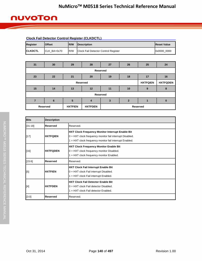
NuMicro M0518 Series Technical Reference Manual
Oct 31, 2014 Page 140 of 497 Revision 1.00
NU
MIC
RO
™ M
0518
SE
RIE
S T
EC
HN
ICA
L R
EF
ER
EN
CE
MA
NU
AL
Clock Fail Detector Control Register (CLKDCTL)
Register Offset R/W Description Reset Value
CLKDCTL CLK_BA+0x70 R/W Clock Fail Detector Control Register 0x0000_0000
31 30 29 28 27 26 25 24
Reserved
23 22 21 20 19 18 17 16
Reserved HXTFQIEN HXTFQDEN
15 14 13 12 11 10 9 8
Reserved
7 6 5 4 3 2 1 0
Reserved HXTFIEN HXTFDEN Reserved
Bits Description
[31:18] Reserved Reserved.
[17] HXTFQIEN
HXT Clock Frequency Monitor Interrupt Enable Bit
0 = HXT clock frequency monitor fail interrupt Disabled.
1 = HXT clock frequency monitor fail interrupt Enabled.
[16] HXTFQDEN
HXT Clock Frequency Monitor Enable Bit
0 = HXT clock frequency monitor Disabled.
1 = HXT clock frequency monitor Enabled.
[15:6] Reserved Reserved.
[5] HXTFIEN
HXT Clock Fail Interrupt Enable Bit
0 = HXT clock Fail interrupt Disabled.
1 = HXT clock Fail interrupt Enabled.
[4] HXTFDEN
HXT Clock Fail Detector Enable Bit
0 = HXT clock Fail detector Disabled.
1 = HXT clock Fail detector Enabled.
[3:0] Reserved Reserved.
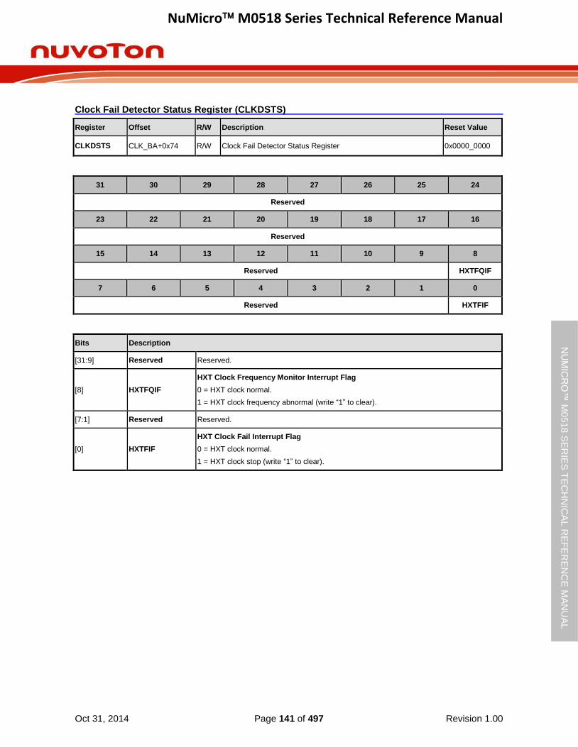
NuMicro M0518 Series Technical Reference Manual
Oct 31, 2014 Page 141 of 497 Revision 1.00
NU
MIC
RO
™ M
0518
SE
RIE
S T
EC
HN
ICA
L R
EF
ER
EN
CE
MA
NU
AL
Clock Fail Detector Status Register (CLKDSTS)
Register Offset R/W Description Reset Value
CLKDSTS CLK_BA+0x74 R/W Clock Fail Detector Status Register 0x0000_0000
31 30 29 28 27 26 25 24
Reserved
23 22 21 20 19 18 17 16
Reserved
15 14 13 12 11 10 9 8
Reserved HXTFQIF
7 6 5 4 3 2 1 0
Reserved HXTFIF
Bits Description
[31:9] Reserved Reserved.
[8] HXTFQIF
HXT Clock Frequency Monitor Interrupt Flag
0 = HXT clock normal.
1 = HXT clock frequency abnormal (write “1” to clear).
[7:1] Reserved Reserved.
[0] HXTFIF
HXT Clock Fail Interrupt Flag
0 = HXT clock normal.
1 = HXT clock stop (write “1” to clear).
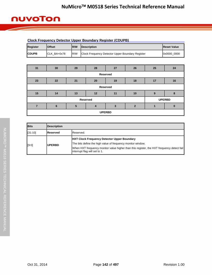
NuMicro M0518 Series Technical Reference Manual
Oct 31, 2014 Page 142 of 497 Revision 1.00
NU
MIC
RO
™ M
0518
SE
RIE
S T
EC
HN
ICA
L R
EF
ER
EN
CE
MA
NU
AL
Clock Frequency Detector Upper Boundary Register (CDUPB)
Register Offset R/W Description Reset Value
CDUPB CLK_BA+0x78 R/W Clock Frequency Detector Upper Boundary Register 0x0000_0000
31 30 29 28 27 26 25 24
Reserved
23 22 21 20 19 18 17 16
Reserved
15 14 13 12 11 10 9 8
Reserved UPERBD
7 6 5 4 3 2 1 0
UPERBD
Bits Description
[31:10] Reserved Reserved.
[9:0] UPERBD
HXT Clock Frequency Detector Upper Boundary
The bits define the high value of frequency monitor window.
When HXT frequency monitor value higher than this register, the HXT frequency detect fail interrupt flag will set to 1.

NuMicro M0518 Series Technical Reference Manual
Oct 31, 2014 Page 143 of 497 Revision 1.00
NU
MIC
RO
™ M
0518
SE
RIE
S T
EC
HN
ICA
L R
EF
ER
EN
CE
MA
NU
AL
Clock Frequency Detector Lower Boundary Register (CDLOWB)
Register Offset R/W Description Reset Value
CDLOWB CLK_BA+0x7C R/W Clock Frequency Detector Lower Boundary Register 0x0000_0000
31 30 29 28 27 26 25 24
Reserved
23 22 21 20 19 18 17 16
Reserved
15 14 13 12 11 10 9 8
Reserved LOWERBD
7 6 5 4 3 2 1 0
LOWERBD
Bits Description
[31:10] Reserved Reserved.
[9:0] LOWERBD
HXT Clock Frequency Detector Lower Boundary
The bits define the low value of frequency monitor window.
When HXT frequency monitor values lower than this register, the HXT frequency detect fail interrupt flag will set to 1.
NuMicro M0518 Series Technical Reference Manual
Oct 31, 2014 Page 144 of 497 Revision 1.00
NU
MIC
RO
™ M
0518
SE
RIE
S T
EC
HN
ICA
L R
EF
ER
EN
CE
MA
NU
AL
6.4 Flash Memory Controller (FMC)
6.4.1 Overview
The NuMicro M0518 series has 68/36K bytes on-chip embedded Flash for application program memory (APROM) that can be updated through ISP procedure. The In-System-Programming (ISP) function enables user to update program memory when chip is soldered on PCB. After chip is powered on, Cortex™-M0 CPU fetches code from APROM or LDROM decided by boot select
(CBS) in CONFIG0. By the way, the NuMicro M0518 series also provides additional Data Flash for user to store some application dependent data.
The NuMicro M0518 supports another flexible feature: configurable Data Flash size. The Data Flash size is decided by Data Flash variable size enable (DFVSEN), Data Flash enable (DFEN) in Config0 and Data Flash base address (DFBADR) in Config1. When DFVSEN is set to 1, the Data Flash size is fixed at 4K and the address is started from 0x0001_f000, and the APROM size is become 64/32K. When DFVSEN is set to 0 and DFEN is set to 1, the Data Flash size is zero and the APROM size is 68/36K bytes. When DFVSEN is set to 0 and DFEN is set to 0, the APROM and Data Flash share 68/36K bytes continuous address and the start address of Data Flash is defined by (DFBADR) in Config1.
6.4.2 Features
Runs up to 50 MHz with zero wait cycle for continuous address read access
All embedded flash memory supports 512 bytes page erase
68/36 KB application program memory (APROM)
4KB In-System-Programming (ISP) loader program memory (LDROM)
Configurable Data Flash size
512 bytes page erase unit
Supports In-Application-Programming (IAP) to switch code between APROM and LDROM without reset
In-System-Programming (ISP) to update on-chip Flash
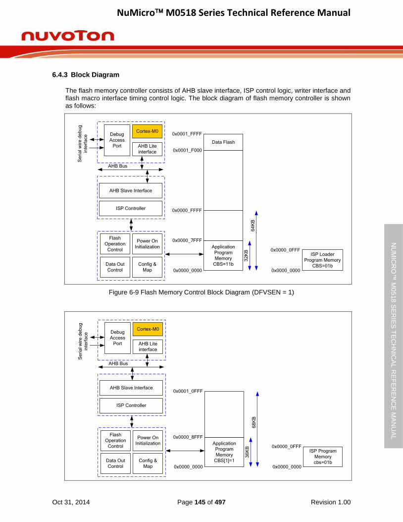
NuMicro M0518 Series Technical Reference Manual
Oct 31, 2014 Page 145 of 497 Revision 1.00
NU
MIC
RO
™ M
0518
SE
RIE
S T
EC
HN
ICA
L R
EF
ER
EN
CE
MA
NU
AL
6.4.3 Block Diagram
The flash memory controller consists of AHB slave interface, ISP control logic, writer interface and flash macro interface timing control logic. The block diagram of flash memory controller is shown as follows:
AHB Slave Interface
ISP Controller
Application
Program
Memory
CBS=11b
0x0000_0000
0x0001_FFFF
Flash
Operation
Control
Power On
Initialization
Data Out
Control
Config &
Map
AHB Bus
32
KB
64
KB
0x0000_7FFF
0x0001_F000
0x0000_0000
0x0000_0FFF
Cortex-M0
AHB Lite
interface
Debug
Access
Port
Se
ria
l w
ire
de
bu
g
inte
rfa
ce
0x0000_FFFF
Data Flash
ISP Loader
Program Memory
CBS=01b
Figure 6-9 Flash Memory Control Block Diagram (DFVSEN = 1)
AHB Slave Interface
ISP Controller
Application
Program
Memory
CBS[1]=1
0x0000_0000
Flash
Operation
Control
Power On
Initialization
Data Out
Control
Config &
Map
AHB Bus
36
KB
68
KB
0x0000_8FFF
0x0000_0000
0x0000_0FFF
Cortex-M0
AHB Lite
interface
Debug
Access
Port
Se
ria
l w
ire
de
bu
g
inte
rfa
ce
0x0001_0FFF
ISP Program
Memory
cbs=01b

NuMicro M0518 Series Technical Reference Manual
Oct 31, 2014 Page 146 of 497 Revision 1.00
NU
MIC
RO
™ M
0518
SE
RIE
S T
EC
HN
ICA
L R
EF
ER
EN
CE
MA
NU
AL
Figure 6-10 Flash Memory Control Block Diagram (DFVSEN = 0)
6.4.4 Functional Description
6.4.4.1 Flash Memory Organization
The NuMicro M0518 series flash memory consists of program memory (APROM), Data Flash, ISP loader program memory (LDROM), and user configuration.
Program memory is main memory for user applications and called APROM. User can write their application to APROM and set system to boot from APROM.
ISP loader program memory is designed for a loader to implement In-System-Programming function. LDROM is independent to APROM and system can also be set to boot from LDROM. Therefore, user can use LDROM to avoid system boot fail when code of APROM was corrupted.
Data Flash is used for user to store data. It can be read by ISP read or memory read and programmed through ISP procedure. The size of each erase unit is 512 bytes. When DFVSEN is set to 1, Data Flash size is always 4 KB and start address is fixed at 0x0001_F000. When DFVSEN is set to 0 and DFEN is set to 1, the Data Flash size is zero and the APROM size is 68/36K bytes. When DFVSEN is set to 0 and DFEN is set to 0, the APROM and Data Flash share 68/36K bytes continuous address and the start address of Data Flash is defined by (DFBADR) in Config1.
User configuration provides several bytes to control system logic, such as flash security lock, boot select, Brown-out voltage level, Data Flash base address, etc…. User configuration works like a fuse for power on setting and loaded from flash memory to its corresponding control registers during chip powered on.
In NuMicro Family, the flash memory organization is different to system memory map. Flash memory organization is used when user using ISP command to read, program or erase flash memory. System memory map is used when CPU access flash memory to fetch code or data. For example, When system is set to boot from LDROM by CBS = 01b, CPU will be able to fetch code of LDROM from 0x0 ~ 0x0FFF. However, if user want to read LDROM by ISP, they still need to read the address of LDROM as 0x0010_0000 ~ 0x0010_0FFF.
Table 6-6 and Figure 6-11 show the address mapping information of APROM, LDROM, Data Flash and user configuration for 36/68 devices.
Block Name Device Type Size Start Address End Address
APROM 36 KB 32 KB 0x0000_0000 0x0000_7FFF
68 KB 64 KB 0x0000_0000 0x0000_FFFF
Data Flash 36 KB 4 KB 0x0001_F000
0x0001_FFFF 68 KB 4 KB 0x0001_F000
LDROM 36/68 KB 4 KB 0x0010_0000 0x0010_0FFF
User Configuration
36/68 KB 2 words 0x0030_0000 0x0030_0004
Table 6-6 Memory Address Map (DFVSEN = 1)
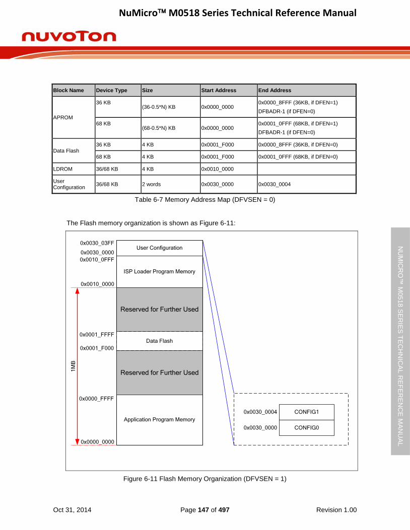
NuMicro M0518 Series Technical Reference Manual
Oct 31, 2014 Page 147 of 497 Revision 1.00
NU
MIC
RO
™ M
0518
SE
RIE
S T
EC
HN
ICA
L R
EF
ER
EN
CE
MA
NU
AL
Block Name Device Type Size Start Address End Address
APROM
36 KB (36-0.5*N) KB 0x0000_0000
0x0000_8FFF (36KB, if DFEN=1)
DFBADR-1 (if DFEN=0)
68 KB (68-0.5*N) KB 0x0000_0000
0x0001_0FFF (68KB, if DFEN=1)
DFBADR-1 (if DFEN=0)
Data Flash 36 KB 4 KB 0x0001_F000 0x0000_8FFF (36KB, if DFEN=0)
68 KB 4 KB 0x0001_F000 0x0001_0FFF (68KB, if DFEN=0)
LDROM 36/68 KB 4 KB 0x0010_0000
User Configuration
36/68 KB 2 words 0x0030_0000 0x0030_0004
Table 6-7 Memory Address Map (DFVSEN = 0)
The Flash memory organization is shown as Figure 6-11:
User Configuration
Application Program Memory
ISP Loader Program Memory
0x0000_0000
0x0010_0000
Reserved for Further Used
0x0001_FFFF
0x0030_0000
0x0030_03FF
CONFIG0
CONFIG1
0x0030_0000
0x0030_0004
0x0010_0FFF
1M
B
Data Flash
Reserved for Further Used
0x0001_F000
0x0000_FFFF
Figure 6-11 Flash Memory Organization (DFVSEN = 1)
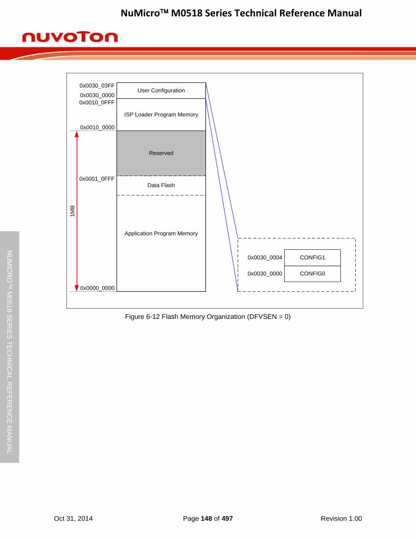
NuMicro M0518 Series Technical Reference Manual
Oct 31, 2014 Page 148 of 497 Revision 1.00
NU
MIC
RO
™ M
0518
SE
RIE
S T
EC
HN
ICA
L R
EF
ER
EN
CE
MA
NU
AL
User Configuration
Application Program Memory
ISP Loader Program Memory
0x0000_0000
0x0010_0000
Reserved
0x0001_0FFF
0x0030_0000
0x0030_03FF
CONFIG0
CONFIG1
0x0030_0000
0x0030_0004
0x0010_0FFF
1M
B
Data Flash
Figure 6-12 Flash Memory Organization (DFVSEN = 0)

NuMicro M0518 Series Technical Reference Manual
Oct 31, 2014 Page 149 of 497 Revision 1.00
NU
MIC
RO
™ M
0518
SE
RIE
S T
EC
HN
ICA
L R
EF
ER
EN
CE
MA
NU
AL
6.4.4.2 User Configuration
User configuration is internal programmable configuration area for boot options. The user configuration is located at 0x300000 of Flash Memory Organization and they are two 32 bits words. Any change on user configuration will take effect after system reboot.
CONFIG0 (Address = 0x0030_0000)
31 30 29 28 27 26 25 24
CWDTEN[2] CWDTPDEN Reserved CGPFMFP CFOSC
23 22 21 20 19 18 17 16
CBODEN CBOV CBORST Reserved
15 14 13 12 11 10 9 8
Reserved CIOINI Reserved
7 6 5 4 3 2 1 0
CBS Reserved CWDTE[1:0] DFVSEN LOCK DFEN
CONFIG0 Address = 0x0030_0000
Bits Description
[31] CWDTEN[2]
Watchdog Timer Hardware Enable Bit
When watchdog timer hardware enable function is enabled, the watchdog enable bit WDTEN (WDT_CTL[7]) and watchdog reset enable bit RSTEN (WDT_CTL[1]) is set to 1 automatically after power on. The clock source of watchdog timer is force at LIRC and LIRC can’t be disabled.
CWDTEN[2:0] is CONFIG0[31][4][3],
011 = WDT hardware enable function is active. WDT clock is always on except chip enters Power- down mode. When chip enter Power-down mode, WDT clock is always on if CWDTPDEN is 0 or WDT clock is controlled by LIRCEN (CLK_PWRCTL[3]) if CWDTPDEN is 1. Please refer to bit field description of CWDTPDEN.
111 = WDT hardware enable function is inactive.
Others = WDT hardware enable function is active. WDT clock is always on.
[30] CWDTPDEN
Watchdog Clock Power-down Enable Bit
0 = OSC10K Watchdog Timer clock source is forced to be always enabled.
1 = OSC10K Watchdog Timer clock source is controlled by OSC10K_EN (PWRCON[3]) when chip enters Power-down.
Note: This bit only works at CWDTEN is set to 0.
[29] Reserved Reserved
[27] CGPFMFP
GPF Multi-function Selection
0 = XT1_IN and XT1_OUT pin is configured as GPIO function.
1 = XT1_IN and XT1_OUT pin is used as external 4~24MHz crystal oscillator pin.
Note: XT1_IN, XT1_OUT multi-function can only be changed by CGPFMFP.

NuMicro M0518 Series Technical Reference Manual
Oct 31, 2014 Page 150 of 497 Revision 1.00
NU
MIC
RO
™ M
0518
SE
RIE
S T
EC
HN
ICA
L R
EF
ER
EN
CE
MA
NU
AL
[26:24] CFOSC
CPU Clock Source Selection after Reset
000 = External 4~24 MHz high speed crystal oscillator clock.
111 = Internal RC 22.1184 MHz high speed oscillator clock.
Others = Reserved.
The value of CFOSC will be load to HCLK_S (CLKSEL0[2:0]) in system register after any reset occurs.
[23] CBODEN
Brown-out Detector Enable Bit
0= Brown-out detect Enabled after powered on.
1= Brown-out detect Disabled after powered on.
[22:21] CBOV
Brown-out Voltage Selection
00 = 2.2 V
01 = 2.7 V
10 = 3.7 V
11 = 4.4 V
[20] CBORST
Brown-out Reset Enable Bit
0 = Brown-out reset Enabled after powered on.
1 = Brown-out reset Disabled after powered on.
[19:11] Reserved Reserved
[10] CIOINI
I/O Initial State Select
0 = All GPIO default to be input tri-state mode after powered on.
1 = All GPIO default to be Quasi-bidirectional mode after chip is powered on.
Note: For PF.0 and PF.1, this field is workable only when CGPFMFP (CONFIG0[27]) is set as 0.
[9:8] Reserved Reserved
[7:6] CBS
Chip Boot Selection
00 = Boot from LDROM with IAP function.
01 = Boot from LDROM without IAP function.
10 = Boot from APROM with IAP function.
11 = Boot from APROM without IAP function.
IAP function means APROM and LDROM can be executed and access by CPU without reset. When IAP function enabled, APROM base address is 0x0 and LDROM base address is 0x100000.
[5] Reserved Reserved
[4:3] CWDTEN[1:0]
Watchdog Timer Hardware Enable Bit
When watchdog timer hardware enable function is enabled, the watchdog enable bit WDTEN (WDT_CTL[7]) and watchdog reset enable bit RSTEN (WDT_CTL[1]) is set to 1 automatically after power on. The clock source of watchdog timer is force at LIRC and LIRC can’t be disabled.
CWDTEN[2:0] is CONFIG0[31][4][3],
011 = WDT hardware enable function is active. WDT clock is always on except chip enter Power-down mode. When chip enter Power-down mode, WDT clock is always on if CWDTPDEN is 0 or WDT clock is controlled by LIRCEN (CLK_PWRCTL[3]) if CWDTPDEN is 1. Please refer to bit field description of CWDTPDEN.
111 = WDT hardware enable function is inactive.
Others = WDT hardware enable function is active. WDT clock is always on.

NuMicro M0518 Series Technical Reference Manual
Oct 31, 2014 Page 151 of 497 Revision 1.00
NU
MIC
RO
™ M
0518
SE
RIE
S T
EC
HN
ICA
L R
EF
ER
EN
CE
MA
NU
AL
[2] DFVSEN
DATA Flash Variable Size Enable
0 = Data flash size is variable and it base address is based on DFBADR (Config1).
1 = Data flash size is fixed at 4K bytes.
[1] LOCK
Security Lock
0 = Flash data is locked.
1 = Flash data is not locked.
When flash data is locked, only device ID, CONFIG0 and CONFIG1 can be read by writer and ICP through serial debug interface. Others data is locked as 0xFFFFFFFF. ISP can read data anywhere regardless of LOCK bit value.
User need to erase whole chip by ICP/Writer tool or erase user configuration by ISP to unlock.
[0] DFEN
Data Flash Enable Bit
0 = Data Flash Enabled.
1 = Data Flash Disabled.
Note: This bit only workable if DFVSEN is set to 0. When DFVSEN is 0 and DFEN is 1, there is no data flash and APROM size is 68K bytes. When DFVSEN is 0 and DFEN is 0, the data flash is shared with APROM within 68K bytes, and the base address of data flash is decided by DFBADR (Config1)
Brown-out detection function is for monitoring the voltage on VDD pin. If VDD voltage falls below level setting of CBOV, the BOD event will be triggered when BOD enabled. User can decide to use BOD reset by enable CBORST or just enable BOD interrupt by NVIC when BOD detected. Because BOD reset is issued whenever VDD voltage falls below the level setting of CBOV, user must make sure the CBOV setting to avoid BOD reset right after BOD reset enabled. For example, if the VDD is 3.3V, CBOV could only be 00’b or 01’b. Otherwise, the system will be halted in BOD reset state when BOD reset is enabled and CBOV is 10’b or 11’b.
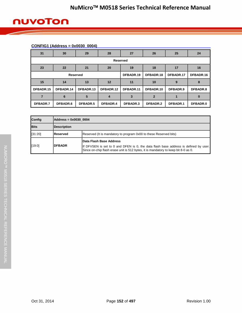
NuMicro M0518 Series Technical Reference Manual
Oct 31, 2014 Page 152 of 497 Revision 1.00
NU
MIC
RO
™ M
0518
SE
RIE
S T
EC
HN
ICA
L R
EF
ER
EN
CE
MA
NU
AL
CONFIG1 (Address = 0x0030_0004)
31 30 29 28 27 26 25 24
Reserved
23 22 21 20 19 18 17 16
Reserved DFBADR.19 DFBADR.18 DFBADR.17 DFBADR.16
15 14 13 12 11 10 9 8
DFBADR.15 DFBADR.14 DFBADR.13 DFBADR.12 DFBADR.11 DFBADR.10 DFBADR.9 DFBADR.8
7 6 5 4 3 2 1 0
DFBADR.7 DFBADR.6 DFBADR.5 DFBADR.4 DFBADR.3 DFBADR.2 DFBADR.1 DFBADR.0
Config Address = 0x0030_0004
Bits Description
[31:20] Reserved Reserved (It is mandatory to program 0x00 to these Reserved bits)
[19:0] DFBADR
Data Flash Base Address
If DFVSEN is set to 0 and DFEN is 0, the data flash base address is defined by user. Since on-chip flash erase unit is 512 bytes, it is mandatory to keep bit 8-0 as 0.
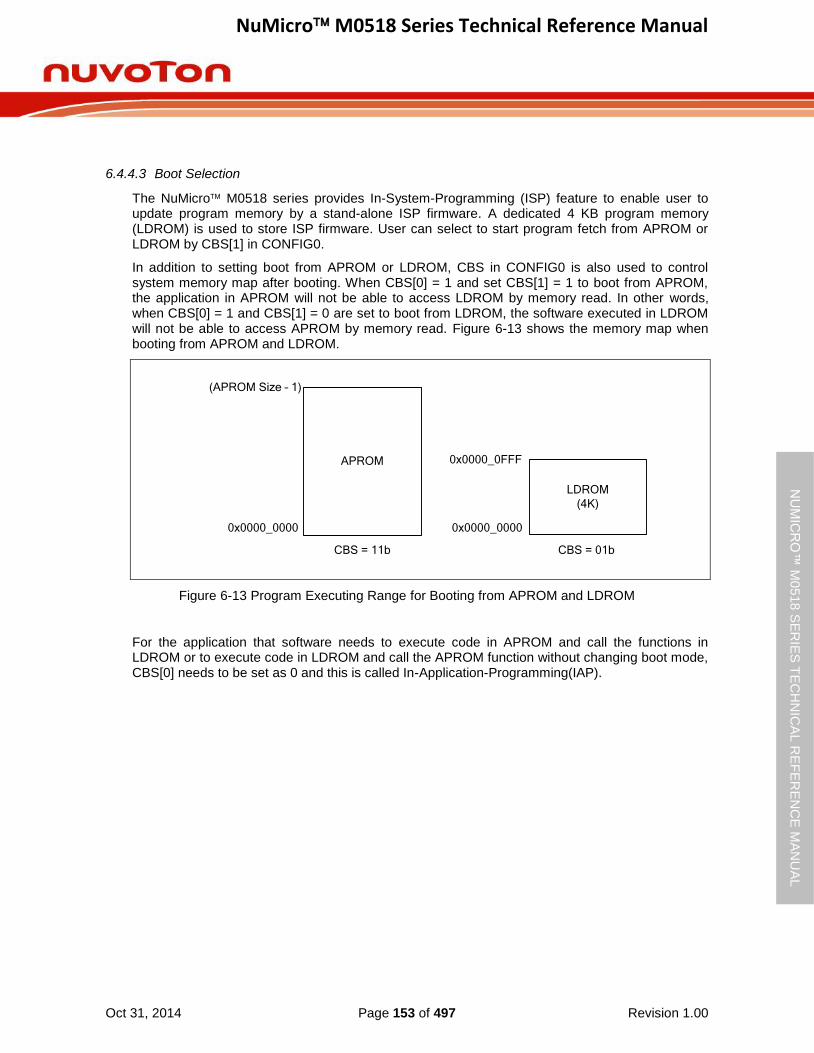
NuMicro M0518 Series Technical Reference Manual
Oct 31, 2014 Page 153 of 497 Revision 1.00
NU
MIC
RO
™ M
0518
SE
RIE
S T
EC
HN
ICA
L R
EF
ER
EN
CE
MA
NU
AL
6.4.4.3 Boot Selection
The NuMicro M0518 series provides In-System-Programming (ISP) feature to enable user to update program memory by a stand-alone ISP firmware. A dedicated 4 KB program memory (LDROM) is used to store ISP firmware. User can select to start program fetch from APROM or LDROM by CBS[1] in CONFIG0.
In addition to setting boot from APROM or LDROM, CBS in CONFIG0 is also used to control system memory map after booting. When CBS[0] = 1 and set CBS[1] = 1 to boot from APROM, the application in APROM will not be able to access LDROM by memory read. In other words, when CBS[0] = 1 and CBS[1] = 0 are set to boot from LDROM, the software executed in LDROM will not be able to access APROM by memory read. Figure 6-13 shows the memory map when booting from APROM and LDROM.
APROM
0x0000_0000
CBS = 11b
LDROM
(4K)
0x0000_0000
CBS = 01b
0x0000_0FFF
(APROM Size – 1)
Figure 6-13 Program Executing Range for Booting from APROM and LDROM
For the application that software needs to execute code in APROM and call the functions in LDROM or to execute code in LDROM and call the APROM function without changing boot mode, CBS[0] needs to be set as 0 and this is called In-Application-Programming(IAP).
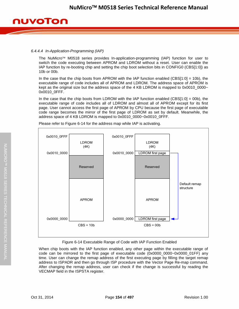
NuMicro M0518 Series Technical Reference Manual
Oct 31, 2014 Page 154 of 497 Revision 1.00
NU
MIC
RO
™ M
0518
SE
RIE
S T
EC
HN
ICA
L R
EF
ER
EN
CE
MA
NU
AL
6.4.4.4 In-Application-Programming (IAP)
The NuMicro M0518 series provides In-application-programming (IAP) function for user to switch the code executing between APROM and LDROM without a reset. User can enable the IAP function by re-booting chip and setting the chip boot selection bits in CONFIG0 (CBS[1:0]) as 10b or 00b.
In the case that the chip boots from APROM with the IAP function enabled (CBS[1:0] = 10b), the executable range of code includes all of APROM and LDROM. The address space of APROM is kept as the original size but the address space of the 4 KB LDROM is mapped to 0x0010_0000~ 0x0010_0FFF.
In the case that the chip boots from LDROM with the IAP function enabled (CBS[1:0] = 00b), the executable range of code includes all of LDROM and almost all of APROM except for its first page. User cannot access the first page of APROM by CPU because the first page of executable code range becomes the mirror of the first page of LDROM as set by default. Meanwhile, the address space of 4 KB LDROM is mapped to 0x0010_0000~0x0010_0FFF.
Please refer to Figure 6-14 for the address map while IAP is activating.
APROM
LDROM
(4K)
0x0000_0000
0x0010_0000
0x0010_0FFF
Reserved
CBS = 10b
APROM
LDROM
(4K)
0x0000_0000
0x0010_0000
0x0010_0FFF
Reserved
CBS = 00b
LDROM first page
LDROM first page
Default remap
structure
Figure 6-14 Executable Range of Code with IAP Function Enabled
When chip boots with the IAP function enabled, any other page within the executable range of code can be mirrored to the first page of executable code (0x0000_0000~0x0000_01FF) any time. User can change the remap address of the first executing page by filling the target remap address to ISPADR and then go through ISP procedure with the Vector Page Re-map command. After changing the remap address, user can check if the change is successful by reading the VECMAP field in the ISPSTA register.
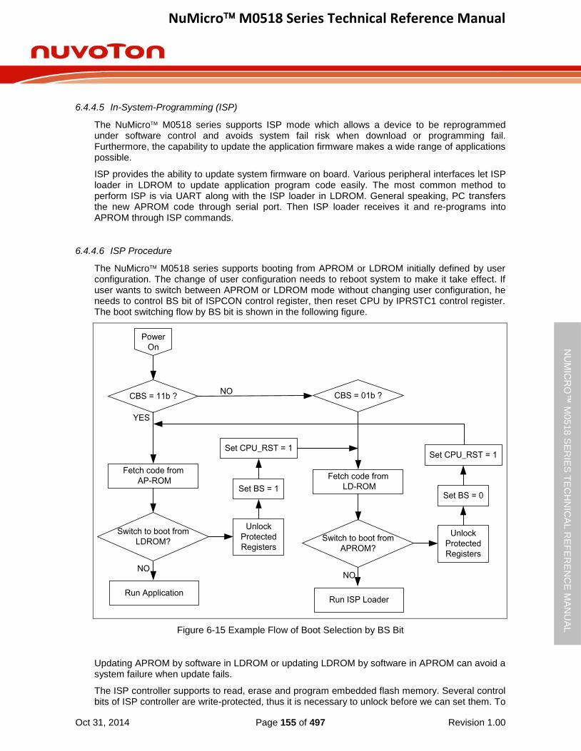
NuMicro M0518 Series Technical Reference Manual
Oct 31, 2014 Page 155 of 497 Revision 1.00
NU
MIC
RO
™ M
0518
SE
RIE
S T
EC
HN
ICA
L R
EF
ER
EN
CE
MA
NU
AL
6.4.4.5 In-System-Programming (ISP)
The NuMicro M0518 series supports ISP mode which allows a device to be reprogrammed under software control and avoids system fail risk when download or programming fail. Furthermore, the capability to update the application firmware makes a wide range of applications possible.
ISP provides the ability to update system firmware on board. Various peripheral interfaces let ISP loader in LDROM to update application program code easily. The most common method to perform ISP is via UART along with the ISP loader in LDROM. General speaking, PC transfers the new APROM code through serial port. Then ISP loader receives it and re-programs into APROM through ISP commands.
6.4.4.6 ISP Procedure
The NuMicro M0518 series supports booting from APROM or LDROM initially defined by user configuration. The change of user configuration needs to reboot system to make it take effect. If user wants to switch between APROM or LDROM mode without changing user configuration, he needs to control BS bit of ISPCON control register, then reset CPU by IPRSTC1 control register. The boot switching flow by BS bit is shown in the following figure.
Power
On
CBS = 11b ?
Fetch code from
AP-ROMFetch code from
LD-ROM
YES
NO
Switch to boot from
LDROM?
CBS = 01b ?
Run Application
Switch to boot from
APROM?
Run ISP Loader
NONO
Set BS = 1
Set CPU_RST = 1
Unlock
Protected
Registers
Set BS = 0
Set CPU_RST = 1
Unlock
Protected
Registers
Figure 6-15 Example Flow of Boot Selection by BS Bit
Updating APROM by software in LDROM or updating LDROM by software in APROM can avoid a system failure when update fails.
The ISP controller supports to read, erase and program embedded flash memory. Several control bits of ISP controller are write-protected, thus it is necessary to unlock before we can set them. To

NuMicro M0518 Series Technical Reference Manual
Oct 31, 2014 Page 156 of 497 Revision 1.00
NU
MIC
RO
™ M
0518
SE
RIE
S T
EC
HN
ICA
L R
EF
ER
EN
CE
MA
NU
AL
unlock the protected register bits, software needs to write 0x59, 0x16 and 0x88 sequentially to REGWRPROT. If register is unlocked successfully, the value of REGWRPROT will be 1. The unlock sequence must not be interrupted by other access; otherwise it may fail to unlock.
After unlocking the protected register bits, user needs to set the ISPCON control register to decide to update LDROM, User Configuration, APROM and enable ISP controller.
Once the ISPCON register is set properly, user can set ISPCMD for erase, read or programming. Set ISPADR for target flash memory based on flash memory origination. ISPDAT can be used to set the data to program or used to return the read data according to ISPCMD.
Finally, set ISPGO bit of ISPTRG control register to perform the relative ISP function. The ISPGO bit is self-cleared when ISP function has been done. To make sure ISP function has been finished before CPU goes ahead, ISB instruction is used right after ISPGO setting.
Several error conditions are checked after ISP is completed. If an error condition occurs, ISP operation is not started and the ISP fail flag will be set instead. ISPFF flag can only be cleared by software. The next ISP procedure can be started even ISPFF bit is kept as 1. Therefore, it is recommended to check the ISPFF bit and clear it after each ISP operation if it is set to 1.
When the ISPGO bit is set, CPU will wait for ISP operation to finish during this period; the peripheral still keeps working as usual. If any interrupt request occurs, CPU will not service it till ISP operation is finished. When ISP operation is finished, the ISPGO bit will be cleared by hardware automatically. User can check whether ISP operation is finished or not by the ISPGO bit. User should add ISB instruction next to the instruction in which ISPGO bit is set 1 to ensure correct execution of the instructions following ISP operation.
Enable ISPEN
Set ISPGO = 1
End of ISP
Operation
?
(Read ISPDAT)
&
Check ISPFF = 1?
YES
End of Flash
Operation
NO
Write
ISPADR/ ISPCMD/
ISPDAT ?
Add ISB instruction
Check ISPGO = 0
?
NO
YES
Start
Stop
Figure 6-16 ISP Flow Example
NuMicro M0518 Series Technical Reference Manual
Oct 31, 2014 Page 157 of 497 Revision 1.00
NU
MIC
RO
™ M
0518
SE
RIE
S T
EC
HN
ICA
L R
EF
ER
EN
CE
MA
NU
AL
ISP Command ISPCMD ISPADR ISPDAT
FLASH Page Erase 0x22 Valid address of flash memory origination.
It must be 512 bytes page alignment. N/A
FLASH Program 0x21 Valid address of flash memory origination Programming Data
FLASH Read 0x00 Valid address of flash memory origination Return Data
Read Unique ID 0x04
0x0000_0000 Unique ID Word 0
0x0000_0004 Unique ID Word 1
0x0000_0008 Unique ID Word 2
Vector Page Re-Map 0x2E Page in APROM or LDROM
It must be 512 bytes page alignment N/A
Table 6-8 ISP Command List
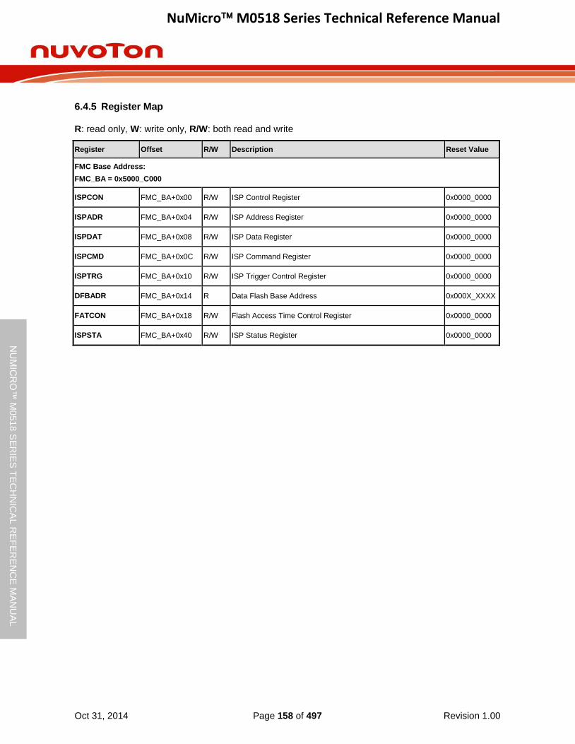
NuMicro M0518 Series Technical Reference Manual
Oct 31, 2014 Page 158 of 497 Revision 1.00
NU
MIC
RO
™ M
0518
SE
RIE
S T
EC
HN
ICA
L R
EF
ER
EN
CE
MA
NU
AL
6.4.5 Register Map
R: read only, W: write only, R/W: both read and write
Register Offset R/W Description Reset Value
FMC Base Address:
FMC_BA = 0x5000_C000
ISPCON FMC_BA+0x00 R/W ISP Control Register 0x0000_0000
ISPADR FMC_BA+0x04 R/W ISP Address Register 0x0000_0000
ISPDAT FMC_BA+0x08 R/W ISP Data Register 0x0000_0000
ISPCMD FMC_BA+0x0C R/W ISP Command Register 0x0000_0000
ISPTRG FMC_BA+0x10 R/W ISP Trigger Control Register 0x0000_0000
DFBADR FMC_BA+0x14 R Data Flash Base Address 0x000X_XXXX
FATCON FMC_BA+0x18 R/W Flash Access Time Control Register 0x0000_0000
ISPSTA FMC_BA+0x40 R/W ISP Status Register 0x0000_0000

NuMicro M0518 Series Technical Reference Manual
Oct 31, 2014 Page 159 of 497 Revision 1.00
NU
MIC
RO
™ M
0518
SE
RIE
S T
EC
HN
ICA
L R
EF
ER
EN
CE
MA
NU
AL
6.4.6 Register Description
ISP Control Register (ISPCON)
Register Offset R/W Description Reset Value
ISPCON FMC_BA+0x00 R/W ISP Control Register 0x0000_0000
31 30 29 28 27 26 25 24
Reserved
23 22 21 20 19 18 17 16
Reserved
15 14 13 12 11 10 9 8
Reserved
7 6 5 4 3 2 1 0
Reserved ISPFF LDUEN CFGUEN APUEN Reserved BS ISPEN
Bits Description
[31:7] Reserved Reserved.
[6] ISPFF
ISP Fail Flag (Write Protect)
This bit is set by hardware when a triggered ISP meets any of the following conditions:
(1) APROM writes to itself if APUEN is set to 0.
(2) LDROM writes to itself if LDUEN is set to 0.
(3) CONFIG is erased/programmed if CFGUEN is set to 0.
(4) Destination address is illegal, such as over an available range.
Write 1 to clear to this bit to 0.
[5] LDUEN
LDROM Update Enable Bit (Write Protect)
0 = LDROM cannot be updated.
1 = LDROM can be updated when chip runs in APROM.
[4] CFGUEN
Enable Config Update By ISP (Write Protect)
0 = ISP update config-bit Disabled.
1 = ISP update config-bit Enabled.
[3] APUEN
APROM Update Enable Bit (Write Protect)
0 = APROM cannot be updated when chip runs in APROM.
1 = APROM can be updated when chip runs in APROM.
[2] Reserved Reserved.

NuMicro M0518 Series Technical Reference Manual
Oct 31, 2014 Page 160 of 497 Revision 1.00
NU
MIC
RO
™ M
0518
SE
RIE
S T
EC
HN
ICA
L R
EF
ER
EN
CE
MA
NU
AL
[1] BS
Boot Select (Write Protect )
Set/clear this bit to select next booting from LDROM/APROM, respectively. This bit also functions as chip booting status flag, which can be used to check where chip booted from. This bit is initiated with the inversed value of CBS in CONFIG0 after any reset is happened except CPU reset (RSTS_CPU is 1) or system reset (RSTS_SYS) is happened.
0 = Boot from APROM.
1 = Boot from LDROM.
[0] ISPEN
ISP Enable Bit (Write Protect )
ISP function enable bit. Set this bit to enable ISP function.
0 = ISP function Disabled.
1 = ISP function Enabled.

NuMicro M0518 Series Technical Reference Manual
Oct 31, 2014 Page 161 of 497 Revision 1.00
NU
MIC
RO
™ M
0518
SE
RIE
S T
EC
HN
ICA
L R
EF
ER
EN
CE
MA
NU
AL
ISP Address Register (ISPADR)
Register Offset R/W Description Reset Value
ISPADR FMC_BA+0x04 R/W ISP Address Register 0x0000_0000
31 30 29 28 27 26 25 24
ISPADR[31:24]
23 22 21 20 19 18 17 16
ISPADR[23:16]
15 14 13 12 11 10 9 8
ISPADR[15:8]
7 6 5 4 3 2 1 0
ISPADR[7:0]
Bits Description
[31:0] ISPADR
ISP Address
The NuMicro M0518 series has a maximum of 17Kx32 (68 KB) embedded Flash, which supports word program only. ISPADR[1:0] must be kept 00b for ISP operation.
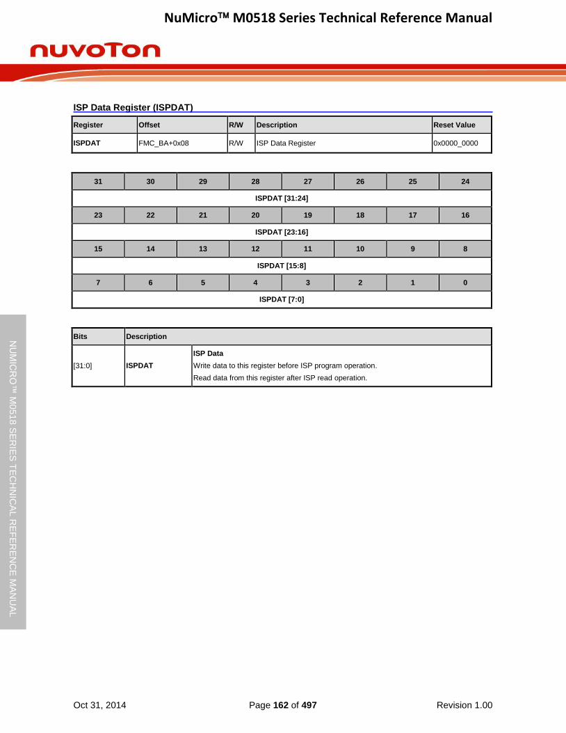
NuMicro M0518 Series Technical Reference Manual
Oct 31, 2014 Page 162 of 497 Revision 1.00
NU
MIC
RO
™ M
0518
SE
RIE
S T
EC
HN
ICA
L R
EF
ER
EN
CE
MA
NU
AL
ISP Data Register (ISPDAT)
Register Offset R/W Description Reset Value
ISPDAT FMC_BA+0x08 R/W ISP Data Register 0x0000_0000
31 30 29 28 27 26 25 24
ISPDAT [31:24]
23 22 21 20 19 18 17 16
ISPDAT [23:16]
15 14 13 12 11 10 9 8
ISPDAT [15:8]
7 6 5 4 3 2 1 0
ISPDAT [7:0]
Bits Description
[31:0] ISPDAT
ISP Data
Write data to this register before ISP program operation.
Read data from this register after ISP read operation.

NuMicro M0518 Series Technical Reference Manual
Oct 31, 2014 Page 163 of 497 Revision 1.00
NU
MIC
RO
™ M
0518
SE
RIE
S T
EC
HN
ICA
L R
EF
ER
EN
CE
MA
NU
AL
ISP Command Register (ISPCMD)
Register Offset R/W Description Reset Value
ISPCMD FMC_BA+0x0C R/W ISP Command Register 0x0000_0000
31 30 29 28 27 26 25 24
Reserved
23 22 21 20 19 18 17 16
Reserved
15 14 13 12 11 10 9 8
Reserved
7 6 5 4 3 2 1 0
Reserved ISPCMD
Bits Description
[31:6] Reserved Reserved.
[5:0] ISPCMD
ISP Command
ISP command table is shown below:
0x00 = Read.
0x04 = Read Unique ID.
0x0B = Read Company ID (0xDA).
0x21 = Program.
0x22 = Page Erase.
0x2E = Set Vector Page Re-Map.
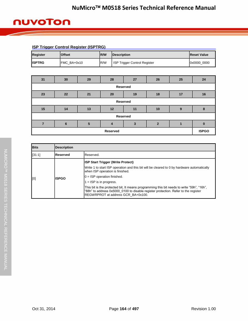
NuMicro M0518 Series Technical Reference Manual
Oct 31, 2014 Page 164 of 497 Revision 1.00
NU
MIC
RO
™ M
0518
SE
RIE
S T
EC
HN
ICA
L R
EF
ER
EN
CE
MA
NU
AL
ISP Trigger Control Register (ISPTRG)
Register Offset R/W Description Reset Value
ISPTRG FMC_BA+0x10 R/W ISP Trigger Control Register 0x0000_0000
31 30 29 28 27 26 25 24
Reserved
23 22 21 20 19 18 17 16
Reserved
15 14 13 12 11 10 9 8
Reserved
7 6 5 4 3 2 1 0
Reserved ISPGO
Bits Description
[31:1] Reserved Reserved.
[0] ISPGO
ISP Start Trigger (Write Protect)
Write 1 to start ISP operation and this bit will be cleared to 0 by hardware automatically when ISP operation is finished.
0 = ISP operation finished.
1 = ISP is in progress.
This bit is the protected bit, It means programming this bit needs to write “59h”, “16h”, “88h” to address 0x5000_0100 to disable register protection. Refer to the register REGWRPROT at address GCR_BA+0x100.

NuMicro M0518 Series Technical Reference Manual
Oct 31, 2014 Page 165 of 497 Revision 1.00
NU
MIC
RO
™ M
0518
SE
RIE
S T
EC
HN
ICA
L R
EF
ER
EN
CE
MA
NU
AL
Data Flash Base Address Register (DFBADR)
Register Offset R/W Description Reset Value
DFBADR FMC_BA+0x14 R Data Flash Base Address 0x000X_XXXX
31 30 29 28 27 26 25 24
DFBADR[31:23]
23 22 21 20 19 18 17 16
DFBADR[23:16]
15 14 13 12 11 10 9 8
DFBADR[15:8]
7 6 5 4 3 2 1 0
DFBADR[7:0]
Bits Description
[31:0] DFBADR
Data Flash Base Address
This register indicates Data Flash start address. It is read only.
When DFVSEN is set to 0, the data flash is shared with APROM. The data flash size is defined by user configuration and the content of this register is loaded from Config1.
When DFVSEN is set to 1, the data flash size is fixed as 4K and the start address can be read from this register is fixed at 0x0001_F000.
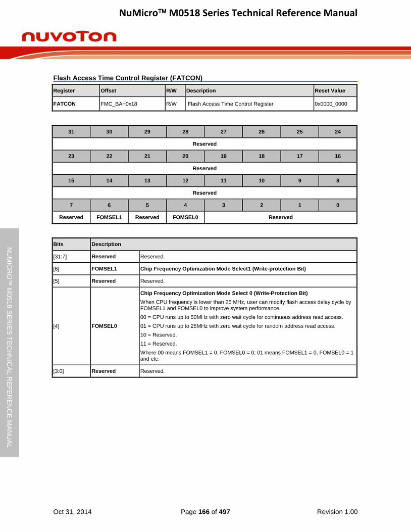
NuMicro M0518 Series Technical Reference Manual
Oct 31, 2014 Page 166 of 497 Revision 1.00
NU
MIC
RO
™ M
0518
SE
RIE
S T
EC
HN
ICA
L R
EF
ER
EN
CE
MA
NU
AL
Flash Access Time Control Register (FATCON)
Register Offset R/W Description Reset Value
FATCON FMC_BA+0x18 R/W Flash Access Time Control Register 0x0000_0000
31 30 29 28 27 26 25 24
Reserved
23 22 21 20 19 18 17 16
Reserved
15 14 13 12 11 10 9 8
Reserved
7 6 5 4 3 2 1 0
Reserved FOMSEL1 Reserved FOMSEL0 Reserved
Bits Description
[31:7] Reserved Reserved.
[6] FOMSEL1 Chip Frequency Optimization Mode Select1 (Write-protection Bit)
[5] Reserved Reserved.
[4] FOMSEL0
Chip Frequency Optimization Mode Select 0 (Write-Protection Bit)
When CPU frequency is lower than 25 MHz, user can modify flash access delay cycle by FOMSEL1 and FOMSEL0 to improve system performance.
00 = CPU runs up to 50MHz with zero wait cycle for continuous address read access.
01 = CPU runs up to 25MHz with zero wait cycle for random address read access.
10 = Reserved.
11 = Reserved.
Where 00 means FOMSEL1 = 0, FOMSEL0 = 0; 01 means FOMSEL1 = 0, FOMSEL0 = 1 and etc.
[3:0] Reserved Reserved.

NuMicro M0518 Series Technical Reference Manual
Oct 31, 2014 Page 167 of 497 Revision 1.00
NU
MIC
RO
™ M
0518
SE
RIE
S T
EC
HN
ICA
L R
EF
ER
EN
CE
MA
NU
AL
ISP Status Register (ISPSTA)
Register Offset R/W Description Reset Value
ISPSTA FMC_BA+0x40 R/W ISP Status Register 0x0000_0000
31 30 29 28 27 26 25 24
Reserved
23 22 21 20 19 18 17 16
Reserved VECMAP[11:7]
15 14 13 12 11 10 9 8
VECMAP[6:0] Reserved
7 6 5 4 3 2 1 0
Reserved ISPFF Reserved CBS ISPGO
Bits Description
[31:21] Reserved Reserved.
[20:9] VECMAP
Vector Page Mapping Address (Read Only)
The current flash address space 0x0000_0000~0x0000_01FF is mapping to address {VECMAP[11:0], 9’h000} ~ {VECMAP[11:0], 9’h1FF}.
[8:7] Reserved Reserved.
[6] ISPFF
ISP Fail Flag (Write-Protection Bit)
This bit is set by hardware when a triggered ISP meets any of the following conditions:
(1) APROM writes to itself
(2) LDROM writes to itself
(3) CONFIG is erased/programmed if CFGUEN is set to 0
(4) Destination address is illegal, such as over an available range
Write 1 to clear this bit.
Note: The function of this bit is the same as ISPCON bit6.
[5:3] Reserved Reserved.
[2:1] CBS Chip Boot Selection (Read Only)
This is a mirror of CBS in CONFIG0.
[0] ISPGO
ISP Start Trigger (Read Only)
Write 1 to start ISP operation and this bit will be cleared to 0 by hardware automatically when ISP operation is finished.
0 = ISP operation finished.
1 = ISP operation progressed.
Note: This bit is the same as ISPTRG bit0.
NuMicro M0518 Series Technical Reference Manual
Oct 31, 2014 Page 168 of 497 Revision 1.00
NU
MIC
RO
™ M
0518
SE
RIE
S T
EC
HN
ICA
L R
EF
ER
EN
CE
MA
NU
AL
6.5 General Purpose I/O (GPIO)
6.5.1 Overview
The NuMicro M0518 series has up to 56 General Purpose I/O pins to be shared with other function pins depending on the chip configuration. These 56 pins are arranged in 6 ports named as GPIOA, GPIOB, GPIOC, GPIOD, GPIOE and GPIOF. The GPIOA/B port has the maximum of 16 pins. The GPIOC port has the maximum of 12 pins. The GPIOD port has the maximum of 4 pins. The GPIOE port has the maximum of 1 pin. The GPIOF port has the maximum of 7 pins. Each of the 56 pins is independent and has the corresponding register bits to control the pin mode function and data.
The I/O type of each of I/O pins can be configured by software individually as input, output, open-drain or Quasi-bidirectional mode. After reset, the I/O mode of all pins are depending on Config0[10] setting. In Quasi-bidirectional mode, I/O pin has a very weak individual pull-up
resistor which is about 110~300 K for VDD from 5.0 V to 2.5 V.
6.5.2 Features
Four I/O modes:
- Quasi-bidirectional
- Push-Pull output
- Open-Drain output
- Input only with high impendence
TTL/Schmitt trigger input selectable by GPx_TYPE[15:0] in GPx_MFP[31:16]
I/O pin configured as interrupt source with edge/level setting
Configurable default I/O mode of all pins after reset by Config0[10] setting
- If Config[10] is 0, all GPIO pins in input tri-state mode after chip reset
- If Config[10] is 1, all GPIO pins in Quasi-bidirectional mode after chip reset
I/O pin internal pull-up resistor enabled only in Quasi-bidirectional I/O mode
Enabling the pin interrupt function will also enable the pin wake-up function
6.5.3 Basic Configuration
The GPIO pin functions are configured in GPA_MFP, GPB_MFP, GPC_MFP, GPD_MFP, GPE_MFP, GPF_MFP, ALT_MFP, ALT_MFP2, ALT_MFP3, and ALT_MFP4 registers.

NuMicro M0518 Series Technical Reference Manual
Oct 31, 2014 Page 169 of 497 Revision 1.00
NU
MIC
RO
™ M
0518
SE
RIE
S T
EC
HN
ICA
L R
EF
ER
EN
CE
MA
NU
AL
6.5.4 Functional Description
6.5.4.1 Input Mode Explanation
Set GPIOx_PMD (PMDn[1:0]) to 00b as the GPIOx port [n] pin is in Input mode and the I/O pin is in tri-state (high impedance) without output drive capability. The GPIOx_PIN value reflects the status of the corresponding port pins.
6.5.4.2 Push-pull Output Mode Explanation
Set GPIOx_PMD (PMDn[1:0]) to 01b as the GPIOx port [n] pin is in Push-pull Output mode and the I/O pin supports digital output function with source/sink current capability. The bit value in the corresponding bit [n] of GPIOx_DOUT is driven on the pin.
Port Pin
Input Data
Port Latch
Data
P
N
VDD
Figure 6-17 Push-Pull Output
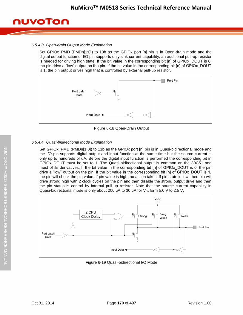
NuMicro M0518 Series Technical Reference Manual
Oct 31, 2014 Page 170 of 497 Revision 1.00
NU
MIC
RO
™ M
0518
SE
RIE
S T
EC
HN
ICA
L R
EF
ER
EN
CE
MA
NU
AL
6.5.4.3 Open-drain Output Mode Explanation
Set GPIOx_PMD (PMDn[1:0]) to 10b as the GPIOx port [n] pin is in Open-drain mode and the digital output function of I/O pin supports only sink current capability, an additional pull-up resistor is needed for driving high state. If the bit value in the corresponding bit [n] of GPIOx_DOUT is 0, the pin drive a “low” output on the pin. If the bit value in the corresponding bit [n] of GPIOx_DOUT is 1, the pin output drives high that is controlled by external pull-up resistor.
Port Pin
Port Latch
DataN
Input Data
Figure 6-18 Open-Drain Output
6.5.4.4 Quasi-bidirectional Mode Explanation
Set GPIOx_PMD (PMDn[1:0]) to 11b as the GPIOx port [n] pin is in Quasi-bidirectional mode and the I/O pin supports digital output and input function at the same time but the source current is only up to hundreds of uA. Before the digital input function is performed the corresponding bit in GPIOx_DOUT must be set to 1. The Quasi-bidirectional output is common on the 80C51 and most of its derivatives. If the bit value in the corresponding bit [n] of GPIOx_DOUT is 0, the pin drive a “low” output on the pin. If the bit value in the corresponding bit [n] of GPIOx_DOUT is 1, the pin will check the pin value. If pin value is high, no action takes. If pin state is low, then pin will drive strong high with 2 clock cycles on the pin and then disable the strong output drive and then the pin status is control by internal pull-up resistor. Note that the source current capability in Quasi-bidirectional mode is only about 200 uA to 30 uA for VDD form 5.0 V to 2.5 V.
Port Pin
2 CPU
Clock Delay
Input Data
Port Latch
Data
P P P
N
VDD
StrongVery
WeakWeak
Figure 6-19 Quasi-bidirectional I/O Mode

NuMicro M0518 Series Technical Reference Manual
Oct 31, 2014 Page 171 of 497 Revision 1.00
NU
MIC
RO
™ M
0518
SE
RIE
S T
EC
HN
ICA
L R
EF
ER
EN
CE
MA
NU
AL
6.5.4.5 GPIO Interrupt and Wake-up Function
Each GPIO pin can be set as chip interrupt source by setting correlative GPIOx_IEN bit and GPIOx_IMD. There are four types of interrupt condition can be selected: low level trigger, high level trigger, falling edge trigger and rising edge trigger. For edge trigger condition, user can enable input signal de-bounce function to prevent unexpected interrupt happened which caused by noise. The de-bounce clock source and sampling cycle can be set through DEBOUNCE register.
The GPIO can also be the chip wake-up source when chip enters Idle mode or Power-down mode. The setting of wake-up trigger condition is the same as GPIO interrupt trigger, but there is one thing need to be noticed if using GPIO as chip wake-up source
To ensure the I/O status before enter into Power-down mode
When using toggle GPIO to wake-up system, user must make sure the I/O status before entering Idle mode or Power-down mode according to the relative wake-up settings.
For example, if configuring the wake-up event occurred by I/O rising edge/high level trigger, user must make sure the I/O status of specified pin is at low level before entering to Idle/Power-down mode; and if configure I/O falling edge/low level trigger to trigger a wake-up event, user must make sure the I/O status of specified pin is at high level before entering to Power-down mode.
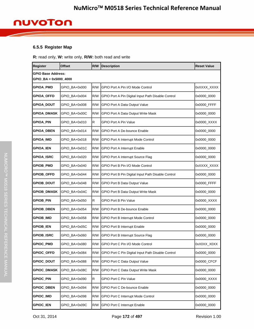
NuMicro M0518 Series Technical Reference Manual
Oct 31, 2014 Page 172 of 497 Revision 1.00
NU
MIC
RO
™ M
0518
SE
RIE
S T
EC
HN
ICA
L R
EF
ER
EN
CE
MA
NU
AL
6.5.5 Register Map
R: read only, W: write only, R/W: both read and write
Register Offset R/W Description Reset Value
GPIO Base Address:
GPIO_BA = 0x5000_4000
GPIOA_PMD GPIO_BA+0x000 R/W GPIO Port A Pin I/O Mode Control 0xXXXX_XXXX
GPIOA_OFFD GPIO_BA+0x004 R/W GPIO Port A Pin Digital Input Path Disable Control 0x0000_0000
GPIOA_DOUT GPIO_BA+0x008 R/W GPIO Port A Data Output Value 0x0000_FFFF
GPIOA_DMASK GPIO_BA+0x00C R/W GPIO Port A Data Output Write Mask 0x0000_0000
GPIOA_PIN GPIO_BA+0x010 R GPIO Port A Pin Value 0x0000_XXXX
GPIOA_DBEN GPIO_BA+0x014 R/W GPIO Port A De-bounce Enable 0x0000_0000
GPIOA_IMD GPIO_BA+0x018 R/W GPIO Port A Interrupt Mode Control 0x0000_0000
GPIOA_IEN GPIO_BA+0x01C R/W GPIO Port A Interrupt Enable 0x0000_0000
GPIOA_ISRC GPIO_BA+0x020 R/W GPIO Port A Interrupt Source Flag 0x0000_0000
GPIOB_PMD GPIO_BA+0x040 R/W GPIO Port B Pin I/O Mode Control 0xXXXX_XXXX
GPIOB_OFFD GPIO_BA+0x044 R/W GPIO Port B Pin Digital Input Path Disable Control 0x0000_0000
GPIOB_DOUT GPIO_BA+0x048 R/W GPIO Port B Data Output Value 0x0000_FFFF
GPIOB_DMASK GPIO_BA+0x04C R/W GPIO Port B Data Output Write Mask 0x0000_0000
GPIOB_PIN GPIO_BA+0x050 R GPIO Port B Pin Value 0x0000_XXXX
GPIOB_DBEN GPIO_BA+0x054 R/W GPIO Port B De-bounce Enable 0x0000_0000
GPIOB_IMD GPIO_BA+0x058 R/W GPIO Port B Interrupt Mode Control 0x0000_0000
GPIOB_IEN GPIO_BA+0x05C R/W GPIO Port B Interrupt Enable 0x0000_0000
GPIOB_ISRC GPIO_BA+0x060 R/W GPIO Port B Interrupt Source Flag 0x0000_0000
GPIOC_PMD GPIO_BA+0x080 R/W GPIO Port C Pin I/O Mode Control 0xX0XX_X0XX
GPIOC_OFFD GPIO_BA+0x084 R/W GPIO Port C Pin Digital Input Path Disable Control 0x0000_0000
GPIOC_DOUT GPIO_BA+0x088 R/W GPIO Port C Data Output Value 0x0000_CFCF
GPIOC_DMASK GPIO_BA+0x08C R/W GPIO Port C Data Output Write Mask 0x0000_0000
GPIOC_PIN GPIO_BA+0x090 R GPIO Port C Pin Value 0x0000_XXXX
GPIOC_DBEN GPIO_BA+0x094 R/W GPIO Port C De-bounce Enable 0x0000_0000
GPIOC_IMD GPIO_BA+0x098 R/W GPIO Port C Interrupt Mode Control 0x0000_0000
GPIOC_IEN GPIO_BA+0x09C R/W GPIO Port C Interrupt Enable 0x0000_0000
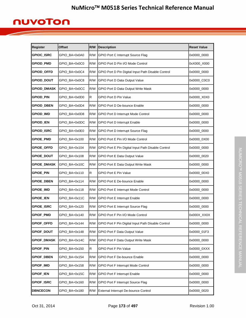
NuMicro M0518 Series Technical Reference Manual
Oct 31, 2014 Page 173 of 497 Revision 1.00
NU
MIC
RO
™ M
0518
SE
RIE
S T
EC
HN
ICA
L R
EF
ER
EN
CE
MA
NU
AL
Register Offset R/W Description Reset Value
GPIOC_ISRC GPIO_BA+0x0A0 R/W GPIO Port C Interrupt Source Flag 0x0000_0000
GPIOD_PMD GPIO_BA+0x0C0 R/W GPIO Port D Pin I/O Mode Control 0xX000_X000
GPIOD_OFFD GPIO_BA+0x0C4 R/W GPIO Port D Pin Digital Input Path Disable Control 0x0000_0000
GPIOD_DOUT GPIO_BA+0x0C8 R/W GPIO Port D Data Output Value 0x0000_C0C0
GPIOD_DMASK GPIO_BA+0x0CC R/W GPIO Port D Data Output Write Mask 0x0000_0000
GPIOD_PIN GPIO_BA+0x0D0 R GPIO Port D Pin Value 0x0000_X0X0
GPIOD_DBEN GPIO_BA+0x0D4 R/W GPIO Port D De-bounce Enable 0x0000_0000
GPIOD_IMD GPIO_BA+0x0D8 R/W GPIO Port D Interrupt Mode Control 0x0000_0000
GPIOD_IEN GPIO_BA+0x0DC R/W GPIO Port D Interrupt Enable 0x0000_0000
GPIOD_ISRC GPIO_BA+0x0E0 R/W GPIO Port D Interrupt Source Flag 0x0000_0000
GPIOE_PMD GPIO_BA+0x100 R/W GPIO Port E Pin I/O Mode Control 0x0000_0X00
GPIOE_OFFD GPIO_BA+0x104 R/W GPIO Port E Pin Digital Input Path Disable Control 0x0000_0000
GPIOE_DOUT GPIO_BA+0x108 R/W GPIO Port E Data Output Value 0x0000_0020
GPIOE_DMASK GPIO_BA+0x10C R/W GPIO Port E Data Output Write Mask 0x0000_0000
GPIOE_PIN GPIO_BA+0x110 R GPIO Port E Pin Value 0x0000_00X0
GPIOE_DBEN GPIO_BA+0x114 R/W GPIO Port E De-bounce Enable 0x0000_0000
GPIOE_IMD GPIO_BA+0x118 R/W GPIO Port E Interrupt Mode Control 0x0000_0000
GPIOE_IEN GPIO_BA+0x11C R/W GPIO Port E Interrupt Enable 0x0000_0000
GPIOE_ISRC GPIO_BA+0x120 R/W GPIO Port E Interrupt Source Flag 0x0000_0000
GPIOF_PMD GPIO_BA+0x140 R/W GPIO Port F Pin I/O Mode Control 0x000X_XX0X
GPIOF_OFFD GPIO_BA+0x144 R/W GPIO Port F Pin Digital Input Path Disable Control 0x0000_0000
GPIOF_DOUT GPIO_BA+0x148 R/W GPIO Port F Data Output Value 0x0000_01F3
GPIOF_DMASK GPIO_BA+0x14C R/W GPIO Port F Data Output Write Mask 0x0000_0000
GPIOF_PIN GPIO_BA+0x150 R GPIO Port F Pin Value 0x0000_0XXX
GPIOF_DBEN GPIO_BA+0x154 R/W GPIO Port F De-bounce Enable 0x0000_0000
GPIOF_IMD GPIO_BA+0x158 R/W GPIO Port F Interrupt Mode Control 0x0000_0000
GPIOF_IEN GPIO_BA+0x15C R/W GPIO Port F Interrupt Enable 0x0000_0000
GPIOF_ISRC GPIO_BA+0x160 R/W GPIO Port F Interrupt Source Flag 0x0000_0000
DBNCECON GPIO_BA+0x180 R/W External Interrupt De-bounce Control 0x0000_0020
NuMicro M0518 Series Technical Reference Manual
Oct 31, 2014 Page 174 of 497 Revision 1.00
NU
MIC
RO
™ M
0518
SE
RIE
S T
EC
HN
ICA
L R
EF
ER
EN
CE
MA
NU
AL
Register Offset R/W Description Reset Value
PAn_PDIO
n=0,1..15
GPIO_BA+0x200
+ 0x04 * n R/W GPIO PA.n Pin Data Input/Output 0x0000_000X
PBn_PDIO
n=0,1..15
GPIO_BA+0x240
+ 0x04 * n R/W GPIO PB.n Pin Data Input/Output 0x0000_000X
PCn_PDIO
n=0~3, 6~11, 14, 15
GPIO_BA+0x280
+ 0x04 * n R/W GPIO PC.n Pin Data Input/Output 0x0000_000X
PDn_PDIO
n=6, 7, 14, 15
GPIO_BA+0x2C0
+ 0x04 * n R/W GPIO PD.n Pin Data Input/Output 0x0000_000X
PEn_PDIO
n=5
GPIO_BA+0x300
+ 0x04 * n R/W GPIO PE.n Pin Data Input/Output 0x0000_000X
PFn_PDIO
n=0,1, 4, 8
GPIO_BA+0x340
+ 0x04 * n R/W GPIO PF.n Pin Data Input/Output 0x0000_000X
NuMicro M0518 Series Technical Reference Manual
Oct 31, 2014 Page 175 of 497 Revision 1.00
NU
MIC
RO
™ M
0518
SE
RIE
S T
EC
HN
ICA
L R
EF
ER
EN
CE
MA
NU
AL
6.5.6 Register Description
GPIO Port [A/B/C/D/E/F] Pin I/O Mode Control (GPIOx_PMD)
Register Offset R/W Description Reset Value
GPIOA_PMD GPIO_BA+0x000 R/W GPIO Port A Pin I/O Mode Control 0xXXXX_XXXX
GPIOB_PMD GPIO_BA+0x040 R/W GPIO Port B Pin I/O Mode Control 0xXXXX_XXXX
GPIOC_PMD GPIO_BA+0x080 R/W GPIO Port C Pin I/O Mode Control 0xX0XX_X0XX
GPIOD_PMD GPIO_BA+0x0C0 R/W GPIO Port D Pin I/O Mode Control 0xX000_X000
GPIOE_PMD GPIO_BA+0x100 R/W GPIO Port E Pin I/O Mode Control 0x0000_0X00
GPIOF_PMD GPIO_BA+0x140 R/W GPIO Port F Pin I/O Mode Control 0x000X_XX0X
31 30 29 28 27 26 25 24
PMD15 PMD14 PMD13 PMD12
23 22 21 20 19 18 17 16
PMD11 PMD10 PMD9 PMD8
15 14 13 12 11 10 9 8
PMD7 PMD6 PMD5 PMD4
7 6 5 4 3 2 1 0
PMD3 PMD2 PMD1 PMD0
Bits Description
[2n+1:2n]
n=0,1..15 PMDn
GPIOx I/O Pin[N] Mode Control
Determine each I/O mode of GPIOx pins.
00 = GPIO port [n] pin is in Input mode.
01 = GPIO port [n] pin is in Push-pull Output mode.
10 = GPIO port [n] pin is in Open-drain Output mode.
11 = GPIO port [n] pin is in Quasi-bidirectional mode.
Note1:
n = 0~15 for GPIOA/GPIOB;
n = 0~3, 6~11, 14, 15 for GPIOC;
n = 6, 7, 14, 15 for GPIOD;
n = 5 for GPIOE;
n = 0, 1, 4~8 for GPIOF.
Note2:
The initial value of this field is defined by CIOINI (CONFIG0[10]). If CIOINI is set to 1, the default value is 0xFFFF_FFFF and all pins will be Quasi-bidirectional mode after chip is powered on. If CIOINI is cleared to 0, the default value is 0x0000_0000 and all pins will be input only mode after chip is powered on.

NuMicro M0518 Series Technical Reference Manual
Oct 31, 2014 Page 176 of 497 Revision 1.00
NU
MIC
RO
™ M
0518
SE
RIE
S T
EC
HN
ICA
L R
EF
ER
EN
CE
MA
NU
AL
GPIO Port [A/B/C/D/E/F] Pin Digital Input Path Disable Register (GPIOx_OFFD)
Register Offset R/W Description Reset Value
GPIOA_OFFD GPIO_BA+0x004 R/W GPIO Port A Pin Digital Input Path Disable Register 0x0000_0000
GPIOB_OFFD GPIO_BA+0x044 R/W GPIO Port B Pin Digital Input Path Disable Register 0x0000_0000
GPIOC_OFFD GPIO_BA+0x084 R/W GPIO Port C Pin Digital Input Path Disable Register 0x0000_0000
GPIOD_OFFD GPIO_BA+0x0C4 R/W GPIO Port D Pin Digital Input Path Disable Register 0x0000_0000
GPIOE_OFFD GPIO_BA+0x104 R/W GPIO Port E Pin Digital Input Path Disable Register 0x0000_0000
GPIOF_OFFD GPIO_BA+0x144 R/W GPIO Port F Pin Digital Input Path Disable Register 0x0000_0000
31 30 29 28 27 26 25 24
OFFD
23 22 21 20 19 18 17 16
OFFD
15 14 13 12 11 10 9 8
Reserved
7 6 5 4 3 2 1 0
Reserved
Bits Description
[n+16]
n=0,1..15 OFFD
GPIOx Pin[N] Digital Input Path Disable Bit
Each of these bits is used to control if the digital input path of corresponding GPIO pin is disabled. If input is analog signal, users can disable GPIO digital input path to avoid current leakage.
0 = I/O digital input path Enabled.
1 = I/O digital input path Disabled (digital input tied to low).
Note:
n = 0~15 for GPIOA/GPIOB;
n = 0~3, 6~11, 14, 15 for GPIOC;
n = 6, 7, 14, 15 for GPIOD;
n = 5 for GPIOE;
n = 0, 1, 4~8 for GPIOF.
[15:0] Reserved Reserved.

NuMicro M0518 Series Technical Reference Manual
Oct 31, 2014 Page 177 of 497 Revision 1.00
NU
MIC
RO
™ M
0518
SE
RIE
S T
EC
HN
ICA
L R
EF
ER
EN
CE
MA
NU
AL
GPIO Port [A/B/C/D/E/F] Data Output Value (GPIOx_DOUT)
Register Offset R/W Description Reset Value
GPIOA_DOUT GPIO_BA+0x008 R/W GPIO Port A Data Output Value 0x0000_FFFF
GPIOB_DOUT GPIO_BA+0x048 R/W GPIO Port B Data Output Value 0x0000_FFFF
GPIOC_DOUT GPIO_BA+0x088 R/W GPIO Port C Data Output Value 0x0000_CFCF
GPIOD_DOUT GPIO_BA+0x0C8 R/W GPIO Port D Data Output Value 0x0000_C0C0
GPIOE_DOUT GPIO_BA+0x108 R/W GPIO Port E Data Output Value 0x0000_0020
GPIOF_DOUT GPIO_BA+0x148 R/W GPIO Port F Data Output Value 0x0000_01F3
31 30 29 28 27 26 25 24
Reserved
23 22 21 20 19 18 17 16
Reserved
15 14 13 12 11 10 9 8
DOUT
7 6 5 4 3 2 1 0
DOUT
Bits Description
[31:16] Reserved Reserved.
[n]
n = 0,1..15 DOUT[n]
GPIOx Pin[N] Output Value
Each of these bits controls the status of a GPIO pin when the GPIO pin is configured as Push-pull output, open-drain output or quasi-bidirectional mode.
0 = GPIO port [A/B/C/D/E/F] Pin[n] will drive Low if the GPIO pin is configured as Push-pull output, Open-drain output or Quasi-bidirectional mode.
1 = GPIO port [A/B/C/D/E/F] Pin[n] will drive High if the GPIO pin is configured as Push-pull output or Quasi-bidirectional mode.
Note:
n = 0~15 for GPIOA/GPIOB;
n = 0~3, 6~11, 14, 15 for GPIOC;
n = 6, 7, 14, 15 for GPIOD;
n = 5 for GPIOE;
n = 0, 1, 4~8 for GPIOF.
NuMicro M0518 Series Technical Reference Manual
Oct 31, 2014 Page 178 of 497 Revision 1.00
NU
MIC
RO
™ M
0518
SE
RIE
S T
EC
HN
ICA
L R
EF
ER
EN
CE
MA
NU
AL
GPIO Port [A/B/C/D/E/F] Data Output Write Mask (GPIOx _DMASK)
Register Offset R/W Description Reset Value
GPIOA_DMASK GPIO_BA+0x00C R/W GPIO Port A Data Output Write Mask 0x0000_0000
GPIOB_DMASK GPIO_BA+0x04C R/W GPIO Port B Data Output Write Mask 0x0000_0000
GPIOC_DMASK GPIO_BA+0x08C R/W GPIO Port C Data Output Write Mask 0x0000_0000
GPIOD_DMASK GPIO_BA+0x0CC R/W GPIO Port D Data Output Write Mask 0x0000_0000
GPIOE_DMASK GPIO_BA+0x10C R/W GPIO Port E Data Output Write Mask 0x0000_0000
GPIOF_DMASK GPIO_BA+0x14C R/W GPIO Port F Data Output Write Mask 0x0000_0000
31 30 29 28 27 26 25 24
Reserved
23 22 21 20 19 18 17 16
Reserved
15 14 13 12 11 10 9 8
DMASK
7 6 5 4 3 2 1 0
DMASK
Bits Description
[31:16] Reserved Reserved.
[n]
n = 0,1..15 DMASK[n]
Port [A/B/C/D/E/F] Data Output Write Mask
These bits are used to protect the corresponding register of GPIOx_DOUT[n] bit. When the DMASK[n] bit is set to 1, the corresponding GPIOx_DOUT[n] bit is protected. If the write signal is masked, write data to the protect bit is ignored.
0 = Corresponding GPIOx_DOUT[n] bit can be updated.
1 = Corresponding GPIOx_DOUT[n] bit protected.
Note1:
This function only protects the corresponding GPIOx_DOUT[n] bit, and will not protect the corresponding bit control register (PAn_PDIO, PBn_PDIO, PCn_PDIO, PDn_PDIO, PEn_PDIO and PFn_PDIO).
Note2:
n = 0~15 for GPIOA/GPIOB;
n = 0~3, 6~11, 14, 15 for GPIOC;
n = 6, 7, 14, 15 for GPIOD;
n = 5 for GPIOE;
n = 0, 1, 4~8 for GPIOF.

NuMicro M0518 Series Technical Reference Manual
Oct 31, 2014 Page 179 of 497 Revision 1.00
NU
MIC
RO
™ M
0518
SE
RIE
S T
EC
HN
ICA
L R
EF
ER
EN
CE
MA
NU
AL
GPIO Port [A/B/C/D/E/F] Pin Value (GPIOx _PIN)
Register Offset R/W Description Reset Value
GPIOA_PIN GPIO_BA+0x010 R GPIO Port A Pin Value 0x0000_XXXX
GPIOB_PIN GPIO_BA+0x050 R GPIO Port B Pin Value 0x0000_XXXX
GPIOC_PIN GPIO_BA+0x090 R GPIO Port C Pin Value 0x0000_XXXX
GPIOD_PIN GPIO_BA+0x0D0 R GPIO Port D Pin Value 0x0000_X0X0
GPIOE_PIN GPIO_BA+0x110 R GPIO Port E Pin Value 0x0000_00X0
GPIOF_PIN GPIO_BA+0x150 R GPIO Port F Pin Value 0x0000_0XXX
31 30 29 28 27 26 25 24
Reserved
23 22 21 20 19 18 17 16
Reserved
15 14 13 12 11 10 9 8
PIN
7 6 5 4 3 2 1 0
PIN
Bits Description
[31:16] Reserved Reserved.
[n]
n = 0,1..15 PIN[n]
Port [A/B/C/D/E/F] Pin Values
Each bit of the register reflects the actual status of the respective GPIO pin. If the bit is 1, it indicates the corresponding pin status is high, else the pin status is low.
Note:
n = 0~15 for GPIOA/GPIOB;
n = 0~3, 6~11, 14, 15 for GPIOC;
n = 6, 7, 14, 15 for GPIOD;
n = 5 for GPIOE;
n = 0, 1, 4~8 for GPIOF.

NuMicro M0518 Series Technical Reference Manual
Oct 31, 2014 Page 180 of 497 Revision 1.00
NU
MIC
RO
™ M
0518
SE
RIE
S T
EC
HN
ICA
L R
EF
ER
EN
CE
MA
NU
AL
GPIO Port [A/B/C/D/E/F] De-bounce Enable Register (GPIOx _DBEN)
Register Offset R/W Description Reset Value
GPIOA_DBEN GPIO_BA+0x014 R/W GPIO Port A De-bounce Enable Register 0x0000_0000
GPIOB_DBEN GPIO_BA+0x054 R/W GPIO Port B De-bounce Enable Register 0x0000_0000
GPIOC_DBEN GPIO_BA+0x094 R/W GPIO Port C De-bounce Enable Register 0x0000_0000
GPIOD_DBEN GPIO_BA+0x0D4 R/W GPIO Port D De-bounce Enable Register 0x0000_0000
GPIOE_DBEN GPIO_BA+0x114 R/W GPIO Port E De-bounce Enable Register 0x0000_0000
GPIOF_DBEN GPIO_BA+0x154 R/W GPIO Port F De-bounce Enable Register 0x0000_0000
31 30 29 28 27 26 25 24
Reserved
23 22 21 20 19 18 17 16
Reserved
15 14 13 12 11 10 9 8
DBEN
7 6 5 4 3 2 1 0
DBEN
Bits Description
[31:16] Reserved Reserved.
[n]
n = 0,1..15 DBEN[n]
Port [A/B/C/D/E/F] Input Signal De-Bounce Enable Bit
DBEN[n] is used to enable the de-bounce function for each corresponding bit. If the input signal pulse width cannot be sampled by continuous two de-bounce sample cycle, the input signal transition is seen as the signal bounce and will not trigger the interrupt. The de-bounce clock source is controlled by DBNCECON[4], one de-bounce sample cycle period is controlled by DBNCECON[3:0].
0 = Bit[n] de-bounce function Disabled.
1 = Bit[n] de-bounce function Enabled.
The de-bounce function is valid only for edge triggered interrupt. If the interrupt mode is level triggered, the de-bounce enable bit is ignored.
Note:
n = 0~15 for GPIOA/GPIOB;
n = 0~3, 6~11, 14, 15 for GPIOC;
n = 6, 7, 14, 15 for GPIOD;
n = 5 for GPIOE;
n = 0, 1, 4~8 for GPIOF.
NuMicro M0518 Series Technical Reference Manual
Oct 31, 2014 Page 181 of 497 Revision 1.00
NU
MIC
RO
™ M
0518
SE
RIE
S T
EC
HN
ICA
L R
EF
ER
EN
CE
MA
NU
AL
GPIO Port [A/B/C/D/E/F] Interrupt Mode Control (GPIOx _IMD)
Register Offset R/W Description Reset Value
GPIOA_IMD GPIO_BA+0x018 R/W GPIO Port A Interrupt Mode Control 0x0000_0000
GPIOB_IMD GPIO_BA+0x058 R/W GPIO Port B Interrupt Mode Control 0x0000_0000
GPIOC_IMD GPIO_BA+0x098 R/W GPIO Port C Interrupt Mode Control 0x0000_0000
GPIOD_IMD GPIO_BA+0x0D8 R/W GPIO Port D Interrupt Mode Control 0x0000_0000
GPIOE_IMD GPIO_BA+0x118 R/W GPIO Port E Interrupt Mode Control 0x0000_0000
GPIOF_IMD GPIO_BA+0x158 R/W GPIO Port F Interrupt Mode Control 0x0000_0000
31 30 29 28 27 26 25 24
Reserved
23 22 21 20 19 18 17 16
Reserved
15 14 13 12 11 10 9 8
IMD
7 6 5 4 3 2 1 0
IMD
Bits Description
[31:16] Reserved Reserved.
[n]
n = 0,1..15 IMD[n]
Port [A/B/C/D/E/F] Edge Or Level Detection Interrupt Control
IMD[n] is used to control the interrupt is by level trigger or by edge trigger. If the interrupt is by edge trigger, the trigger source can be controlled by de-bounce. If the interrupt is by level trigger, the input source is sampled by one HCLK clock and generates the interrupt.
0 = Edge trigger interrupt.
1 = Level trigger interrupt.
If the pin is set as the level trigger interrupt, only one level can be set on the registers GPIOx_IEN. If both levels to trigger interrupt are set, the setting is ignored and no interrupt will occur.
The de-bounce function is valid only for edge triggered interrupt. If the interrupt mode is level triggered, the de-bounce enable bit is ignored.
Note:
n = 0~15 for GPIOA/GPIOB;
n = 0~3, 6~11, 14, 15 for GPIOC;
n = 6, 7, 14, 15 for GPIOD;
n = 5 for GPIOE;
n = 0, 1, 4~8 for GPIOF.

NuMicro M0518 Series Technical Reference Manual
Oct 31, 2014 Page 182 of 497 Revision 1.00
NU
MIC
RO
™ M
0518
SE
RIE
S T
EC
HN
ICA
L R
EF
ER
EN
CE
MA
NU
AL
GPIO Port [A/B/C/D/E/F] Interrupt Enable Register (GPIOx _IEN)
Register Offset R/W Description Reset Value
GPIOA_IEN GPIO_BA+0x01C R/W GPIO Port A Interrupt Enable Register 0x0000_0000
GPIOB_IEN GPIO_BA+0x05C R/W GPIO Port B Interrupt Enable Register 0x0000_0000
GPIOC_IEN GPIO_BA+0x09C R/W GPIO Port C Interrupt Enable Register 0x0000_0000
GPIOD_IEN GPIO_BA+0x0DC R/W GPIO Port D Interrupt Enable Register 0x0000_0000
GPIOE_IEN GPIO_BA+0x11C R/W GPIO Port E Interrupt Enable Register 0x0000_0000
GPIOF_IEN GPIO_BA+0x15C R/W GPIO Port F Interrupt Enable Register 0x0000_0000
31 30 29 28 27 26 25 24
IR_EN
23 22 21 20 19 18 17 16
IR_EN
15 14 13 12 11 10 9 8
IF_EN
7 6 5 4 3 2 1 0
IF_EN
Bits Description
[n+16]
n = 0,1..15 IR_EN[n]
Port [A/B/C/D/E/F] Interrupt Enabled By Input Rising Edge Or Input Level High
IR_EN[n] used to enable the interrupt for each of the corresponding input GPIO_PIN[n]. Set bit to 1 also enable the pin wake-up function.
When setting the IR_EN[n] bit to 1:
If the interrupt is level trigger, the input PIN[n] state at level “high” will generate the interrupt.
If the interrupt is edge trigger, the input PIN[n] state change from “low-to-high” will generate the interrupt.
0 = PIN[n] level-high or low-to-high interrupt Disabled.
1 = PIN[n] level-high or low-to-high interrupt Enabled.
Note:
n = 0~15 for GPIOA/GPIOB;
n = 0~3, 6~11, 14, 15 for GPIOC;
n = 6, 7, 14, 15 for GPIOD;
n = 5 for GPIOE;
n = 0, 1, 4~8 for GPIOF.
[n]
n = 0,1..15 IF_EN[n]
Port [A/B/C/D/E/F] Interrupt Enabled By Input Falling Edge Or Input Level Low
IF_EN[n] is used to enable the interrupt for each of the corresponding input GPIO_PIN[n]. Set bit to 1 also enable the pin wake-up function.
When setting the IF_EN[n] bit to 1:
If the interrupt is level trigger, the input PIN[n] state at level “low” will generate the
NuMicro M0518 Series Technical Reference Manual
Oct 31, 2014 Page 183 of 497 Revision 1.00
NU
MIC
RO
™ M
0518
SE
RIE
S T
EC
HN
ICA
L R
EF
ER
EN
CE
MA
NU
AL
interrupt.
If the interrupt is edge trigger, the input PIN[n] state change from “high-to-low” will generate the interrupt.
0 = PIN[n] state low-level or high-to-low change interrupt Disabled.
1 = PIN[n] state low-level or high-to-low change interrupt Enabled.
Note:
n = 0~15 for GPIOA/GPIOB;
n = 0~3, 6~11, 14, 15 for GPIOC;
n = 6, 7, 14, 15 for GPIOD;
n = 5 for GPIOE;
n = 0, 1, 4~8 for GPIOF.

NuMicro M0518 Series Technical Reference Manual
Oct 31, 2014 Page 184 of 497 Revision 1.00
NU
MIC
RO
™ M
0518
SE
RIE
S T
EC
HN
ICA
L R
EF
ER
EN
CE
MA
NU
AL
GPIO Port [A/B/C/D/E/F] Interrupt Source Flag (GPIOx _ISRC)
Register Offset R/W Description Reset Value
GPIOA_ISRC GPIO_BA+0x020 R/W GPIO Port A Interrupt Source Flag 0x0000_0000
GPIOB_ISRC GPIO_BA+0x060 R/W GPIO Port B Interrupt Source Flag 0x0000_0000
GPIOC_ISRC GPIO_BA+0x0A0 R/W GPIO Port C Interrupt Source Flag 0x0000_0000
GPIOD_ISRC GPIO_BA+0x0E0 R/W GPIO Port D Interrupt Source Flag 0x0000_0000
GPIOE_ISRC GPIO_BA+0x120 R/W GPIO Port E Interrupt Source Flag 0x0000_0000
GPIOF_ISRC GPIO_BA+0x160 R/W GPIO Port F Interrupt Source Flag 0x0000_0000
31 30 29 28 27 26 25 24
Reserved
23 22 21 20 19 18 17 16
Reserved
15 14 13 12 11 10 9 8
ISRC
7 6 5 4 3 2 1 0
ISRC
Bits Description
[31:16] Reserved Reserved.
[n]
n = 0,1..15 ISRC[n]
Port [A/B/C/D/E/F] Interrupt Source Flag
Read :
0 = No interrupt at GPIOx[n].
1 = GPIOx[n] generates an interrupt.
Write :
0= No action.
1= Clear the corresponding pending interrupt.
Note:
n = 0~15 for GPIOA/GPIOB;
n = 0~3, 6~11, 14, 15 for GPIOC;
n = 6, 7, 14, 15 for GPIOD;
n = 5 for GPIOE;
n = 0, 1, 4~8 for GPIOF.
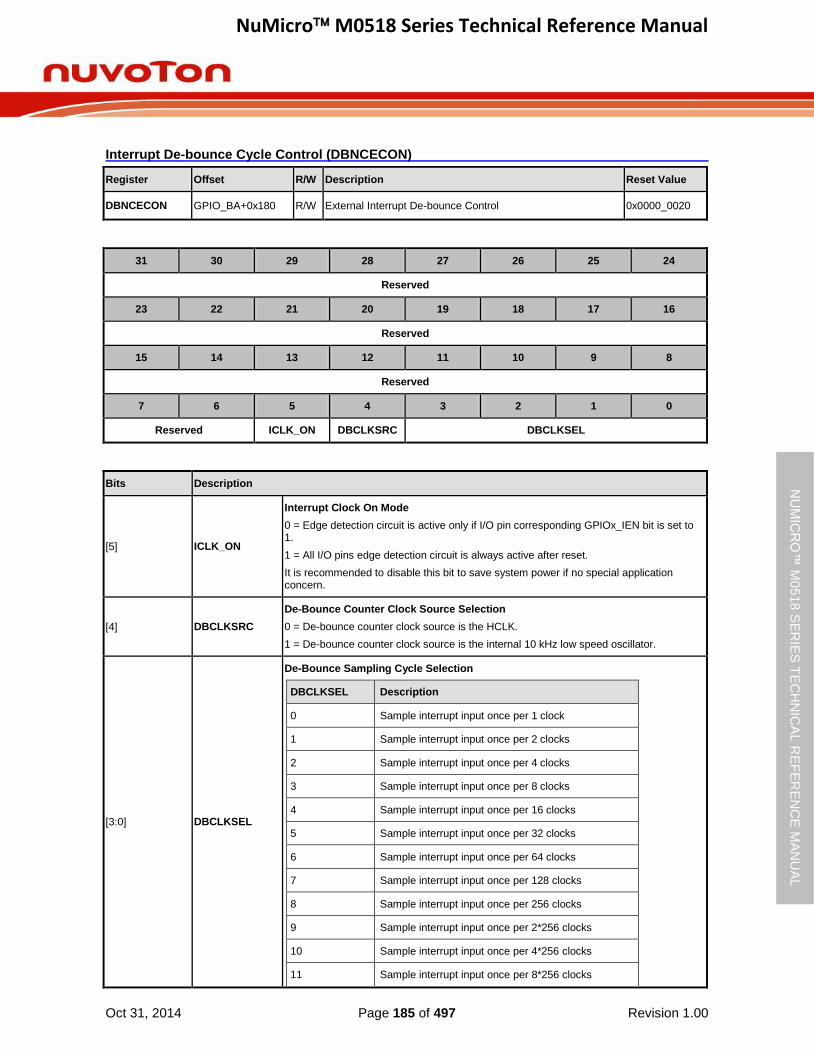
NuMicro M0518 Series Technical Reference Manual
Oct 31, 2014 Page 185 of 497 Revision 1.00
NU
MIC
RO
™ M
0518
SE
RIE
S T
EC
HN
ICA
L R
EF
ER
EN
CE
MA
NU
AL
Interrupt De-bounce Cycle Control (DBNCECON)
Register Offset R/W Description Reset Value
DBNCECON GPIO_BA+0x180 R/W External Interrupt De-bounce Control 0x0000_0020
31 30 29 28 27 26 25 24
Reserved
23 22 21 20 19 18 17 16
Reserved
15 14 13 12 11 10 9 8
Reserved
7 6 5 4 3 2 1 0
Reserved ICLK_ON DBCLKSRC DBCLKSEL
Bits Description
[5] ICLK_ON
Interrupt Clock On Mode
0 = Edge detection circuit is active only if I/O pin corresponding GPIOx_IEN bit is set to 1.
1 = All I/O pins edge detection circuit is always active after reset.
It is recommended to disable this bit to save system power if no special application concern.
[4] DBCLKSRC
De-Bounce Counter Clock Source Selection
0 = De-bounce counter clock source is the HCLK.
1 = De-bounce counter clock source is the internal 10 kHz low speed oscillator.
[3:0] DBCLKSEL
De-Bounce Sampling Cycle Selection
DBCLKSEL Description
0 Sample interrupt input once per 1 clock
1 Sample interrupt input once per 2 clocks
2 Sample interrupt input once per 4 clocks
3 Sample interrupt input once per 8 clocks
4 Sample interrupt input once per 16 clocks
5 Sample interrupt input once per 32 clocks
6 Sample interrupt input once per 64 clocks
7 Sample interrupt input once per 128 clocks
8 Sample interrupt input once per 256 clocks
9 Sample interrupt input once per 2*256 clocks
10 Sample interrupt input once per 4*256 clocks
11 Sample interrupt input once per 8*256 clocks
NuMicro M0518 Series Technical Reference Manual
Oct 31, 2014 Page 186 of 497 Revision 1.00
NU
MIC
RO
™ M
0518
SE
RIE
S T
EC
HN
ICA
L R
EF
ER
EN
CE
MA
NU
AL
12 Sample interrupt input once per 16*256 clocks
13 Sample interrupt input once per 32*256 clocks
14 Sample interrupt input once per 64*256 clocks
15 Sample interrupt input once per 128*256 clocks

NuMicro M0518 Series Technical Reference Manual
Oct 31, 2014 Page 187 of 497 Revision 1.00
NU
MIC
RO
™ M
0518
SE
RIE
S T
EC
HN
ICA
L R
EF
ER
EN
CE
MA
NU
AL
GPIO Px.n Pin Data Input/Output (Pxn_PDIO)
Register Offset R/W Description Reset Value
PAn_PDIO
n = 0,1..15
GPIO_BA+0x200
+ 0x04 * n R/W GPIO PA.n Pin Data Input/Output 0x0000_000X
PBn_PDIO
n = 0,1..15
GPIO_BA+0x240
+ 0x04 * n R/W GPIO PB.n Pin Data Input/Output 0x0000_000X
PCn_PDIO
n = 0~3, 6~11, 14, 15
GPIO_BA+0x280
+ 0x04 * n R/W GPIO PC.n Pin Data Input/Output 0x0000_000X
PDn_PDIO
n = 6, 7, 14, 15
GPIO_BA+0x2C0
+ 0x04 * n R/W GPIO PD.n Pin Data Input/Output 0x0000_000X
PEn_PDIO
n = 5
GPIO_BA+0x300
+ 0x04 * n R/W GPIO PE.n Pin Data Input/Output 0x0000_000X
PFn_PDIO
n = 0, 1, 4~8
GPIO_BA+0x340
+ 0x04 * n R/W GPIO PF.n Pin Data Input/Output 0x0000_000X
Note: x = A/B/C/D/E/F
31 30 29 28 27 26 25 24
Reserved
23 22 21 20 19 18 17 16
Reserved
15 14 13 12 11 10 9 8
Reserved
7 6 5 4 3 2 1 0
Reserved Pxn_PDIO
Bits Description
[0] Pxn_PDIO
GPIO Px.N Pin Data Input/Output
Write this bit can control one GPIO pin output value.
0 = Corresponding GPIO pin set to low.
1 = Corresponding GPIO pin set to high.
Read this register to get GPIO pin status.
For example: writing PA0_PDIO will reflect the written value to bit GPIOA_DOUT[0], read PA0_PDIO will return the value of GPIOA_PIN[0].
Note: The write operation will not be affected by register GPIOx_DMASK.

NuMicro M0518 Series Technical Reference Manual
Oct 31, 2014 Page 188 of 497 Revision 1.00
NU
MIC
RO
™ M
0518
SE
RIE
S T
EC
HN
ICA
L R
EF
ER
EN
CE
MA
NU
AL
6.6 Timer Controller (TIMER)
6.6.1 Overview
The timer controller includes four 32-bit timers, TIMER0 ~ TIMER3, allowing user to easily implement a timer control for applications. The timer can perform functions, such as frequency measurement, delay timing, clock generation, and event counting by external input pins, and interval measurement by external capture pins.
6.6.2 Features
Four sets of 32-bit timers with 24-bit up counter and one 8-bit prescale counter
Independent clock source for each timer
Provides four timer counting modes: one-shot, periodic, toggle and continuous counting
Time-out period = (Period of timer clock input) * (8-bit prescale counter + 1) * (24-bit TCMP)
Maximum counting cycle time = (1 / T MHz) * (28) * (2
24), T is the period of timer clock
24-bit up counter value is readable through TDR (Timer Data Register)
Supports event counting function to count the event from external counter pin (TM0~TM3)
Supports external pin capture (TM0_EXT~TM3_EXT) for interval measurement
Supports external pin capture (TM0_EXT~TM3_EXT) for reset 24-bit up counter
Supports chip wake-up from Idle/Power-down mode if a timer interrupt signal is generated
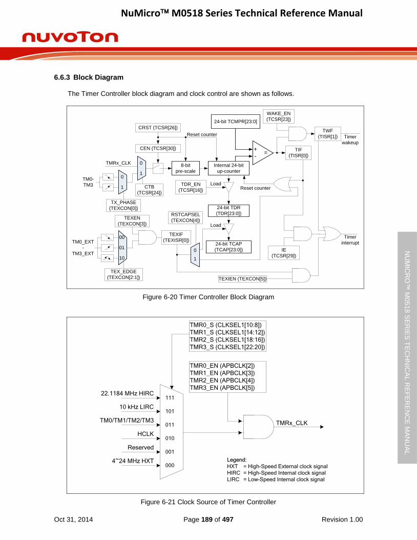
NuMicro M0518 Series Technical Reference Manual
Oct 31, 2014 Page 189 of 497 Revision 1.00
NU
MIC
RO
™ M
0518
SE
RIE
S T
EC
HN
ICA
L R
EF
ER
EN
CE
MA
NU
AL
6.6.3 Block Diagram
The Timer Controller block diagram and clock control are shown as follows.
Timer
interrupt
TM0-
TM3
Internal 24-bit
up-counter
8-bit
pre-scale
0
1
CTB
(TCSR[24])
TMRx_CLK
CEN (TCSR[30])
CRST (TCSR[26])
0
1
TX_PHASE
(TEXCON[0])
Reset counter
24-bit TDR
(TDR[23:0])
24-bit TCMPR[23:0]
+-
=TIF
(TISR[0])
Reset counterTDR_EN
(TCSR[16])
Load
24-bit TCAP
(TCAP[23:0])
00
01
10
TM0_EXT
-
TM3_EXT
TEX_EDGE
(TEXCON[2:1])
TEXEN
(TEXCON[3])
RSTCAPSEL
(TEXCON[4])
TEXIF
(TEXISR[0])
TEXIEN (TEXCON[5])
Load
TWF
(TISR[1])
IE
(TCSR[29])
Timer
wakeup
WAKE_EN
(TCSR[23])
0
1
Figure 6-20 Timer Controller Block Diagram
111
010
001
HCLK
Reserved
4~24 MHz HXT
TMR0_S (CLKSEL1[10:8])
TMR1_S (CLKSEL1[14:12])
TMR2_S (CLKSEL1[18:16])
TMR3_S (CLKSEL1[22:20])
TMR0_EN (APBCLK[2])
TMR1_EN (APBCLK[3])
TMR2_EN (APBCLK[4])
TMR3_EN (APBCLK[5])
TMRx_CLK
22.1184 MHz HIRC
000
011TM0/TM1/TM2/TM3
10110 kHz LIRC
Legend:
HXT = High-Speed External clock signal
HIRC = High-Speed Internal clock signal
LIRC = Low-Speed Internal clock signal
Figure 6-21 Clock Source of Timer Controller
NuMicro M0518 Series Technical Reference Manual
Oct 31, 2014 Page 190 of 497 Revision 1.00
NU
MIC
RO
™ M
0518
SE
RIE
S T
EC
HN
ICA
L R
EF
ER
EN
CE
MA
NU
AL
6.6.4 Basic Configuration
The peripheral clock source of Timer0 ~ Timer3 can be enabled in APBCLK[5:2] and selected as different frequency in CLKSEL1[10:8] for Timer0, CLKSEL1[14:12] for Timer1, CLKSEL1[18:16] for Timer2 and CLKSEL1[22:20] for Timer3.
6.6.5 Functional Description
6.6.5.1 Timer Interrupt Flag
Timer controller supports two interrupt flags; one is TIF flag and its set while timer counter value (TDR) matches the timer compared value (TCMP), the other is TEXIF flag and its set when the transition on the TMx_EXT pin associated TEX_EDGE setting.
6.6.5.2 One–shot Mode
If timer controller is configured at one-shot mode (TCSR[28:27] is 00) and CEN (TCSR[30]) bit is set, the timer counter starts up counting. Once the TDR value reaches TCMP value, the TIF flag will be set to 1, TDR value and CEN bit is cleared by timer controller then timer counting operation stops. In the meantime, if the IE (TCSR[29]) bit is enabled, the timer interrupt signal is generated and sent to NVIC to inform CPU also.
6.6.5.3 Periodic Mode
If timer controller is configured at periodic mode (TCSR[28:27] is 01) and CEN bit is set, the timer counter starts up counting. Once the TDR value reaches TCMP value, the TIF flag will be set to 1, TDR value will be cleared by timer controller and timer counter operates counting again. In the meantime, if the IE bit is enabled, the timer interrupt signal is generated and sent to NVIC to inform CPU also. In this mode, timer controller operates counting and compares with TCMP value periodically until the CEN bit is cleared by software.
6.6.5.4 Toggle-output Mode
If timer controller is configured at toggle-out mode (TCSR[28:27] is 10) and CEN bit is set, the timer counter starts up counting. The counting operation of toggle-out mode is almost the same as periodic mode, except toggle-out mode has associated TM0~TM3 pin to output signal while specify TIF bit is set. Thus, the toggle-output signal on TM0~TM3 pin is changing back and forth with 50% duty cycle.
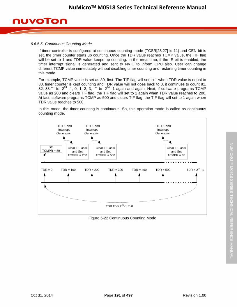
NuMicro M0518 Series Technical Reference Manual
Oct 31, 2014 Page 191 of 497 Revision 1.00
NU
MIC
RO
™ M
0518
SE
RIE
S T
EC
HN
ICA
L R
EF
ER
EN
CE
MA
NU
AL
6.6.5.5 Continuous Counting Mode
If timer controller is configured at continuous counting mode (TCSR[28:27] is 11) and CEN bit is set, the timer counter starts up counting. Once the TDR value reaches TCMP value, the TIF flag will be set to 1 and TDR value keeps up counting. In the meantime, if the IE bit is enabled, the timer interrupt signal is generated and sent to NVIC to inform CPU also. User can change different TCMP value immediately without disabling timer counting and restarting timer counting in this mode.
For example, TCMP value is set as 80, first. The TIF flag will set to 1 when TDR value is equal to 80, timer counter is kept counting and TDR value will not goes back to 0, it continues to count 81, 82, 83,˙˙˙ to 2
24 -1, 0, 1, 2, 3, ˙˙˙ to 2
24 -1 again and again. Next, if software programs TCMP
value as 200 and clears TIF flag, the TIF flag will set to 1 again when TDR value reaches to 200. At last, software programs TCMP as 500 and clears TIF flag, the TIF flag will set to 1 again when TDR value reaches to 500.
In this mode, the timer counting is continuous. So, this operation mode is called as continuous counting mode.
TDR = 0
Set
TCMPR = 80
TIF = 1 and
Interrupt
Generation
Clear TIF as 0
and Set
TCMPR = 200
TDR from 224
-1 to 0
TDR = 100 TDR = 200 TDR = 300 TDR = 400 TDR = 500 TDR = 224
-1
TIF = 1 and
Interrupt
Generation
Clear TIF as 0
and Set
TCMPR = 500
TIF = 1 and
Interrupt
Generation
Clear TIF as 0
and Set
TCMPR = 80
Figure 6-22 Continuous Counting Mode

NuMicro M0518 Series Technical Reference Manual
Oct 31, 2014 Page 192 of 497 Revision 1.00
NU
MIC
RO
™ M
0518
SE
RIE
S T
EC
HN
ICA
L R
EF
ER
EN
CE
MA
NU
AL
6.6.5.6 Event Counting Mode
Timer controller also provides an application which can count the input event from TMx pin (x= 0~3) and the number of event will reflect to TDR value. It is also called as event counting function. In this function, CTB (TCSR[24]) bit should be set and the timer peripheral clock source should be set as HCLK.
Software can enable or disable TMx pin de-bounce circuit by TCDB (TEXCON[7]) bit. The input event frequency should be less than 1/3 HCLK if TMx pin de-bounce disabled or less than 1/8 HCLK if TMx pin de-bounce enabled to assure the returned TDR value is incorrect, and software can also select edge detection phase of TMx pin by TX_PHASE (TEXCON[0]) bit.
In event counting mode, the timer counting operation mode can be selected as one-shot, periodic and continuous counting mode to counts the TDR value by input event from TMx pin.
6.6.5.7 External Capture Mode
The event capture function is used to capture Timer Data Register (TDR) value to Timer Capture Data Register (TCAP) value while edge transition detected on TMx_EXT pin (x= 0~3). In this mode, RSTCAPSEL (TEXCON[4]) bit should be as 0 for select TMx_EXT transition is using as the event capture function and the timer peripheral clock source should be set as HCLK.
Software can enable or disable TxEX pin de-bounce circuit by TEXDB (TEXCON[6]) bit. The transition frequency of TMx_EXT pin should be less than 1/3 HCLK if TMx_EXT pin de-bounce disabled or less than 1/8 HCLK if TMx_EXT pin de-bounce enabled to assure the capture function can be work normally, and software can also select edge transition detection of TMx_EXT pin by TEX_EDGE (TEXCON[2:1]) bits.
In event capture mode, software does not consider what timer counting operation mode is selected, the capture event occurred only if edge transition on TMx_EXT pin is detected.
6.6.5.8 Event Reset Counter Mode
It also provides event reset counter function to reset TDR value while edge transition detected on TMx_EXT pin (x= 0~3). In this mode, most the settings are the same as event capture function except RSTCAPSEL (TEXCON[4]) bit should be as 1 for select TMx_EXT transition is using as the event reset counter.
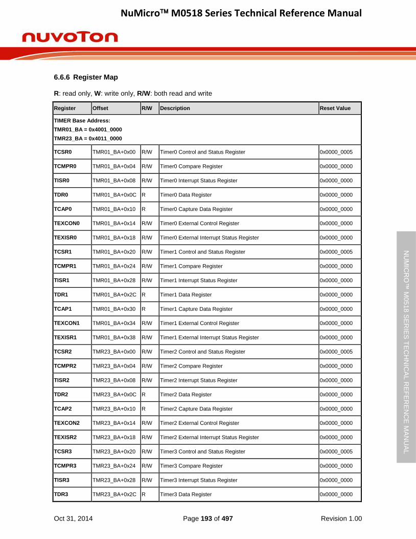
NuMicro M0518 Series Technical Reference Manual
Oct 31, 2014 Page 193 of 497 Revision 1.00
NU
MIC
RO
™ M
0518
SE
RIE
S T
EC
HN
ICA
L R
EF
ER
EN
CE
MA
NU
AL
6.6.6 Register Map
R: read only, W: write only, R/W: both read and write
Register Offset R/W Description Reset Value
TIMER Base Address:
TMR01_BA = 0x4001_0000
TMR23_BA = 0x4011_0000
TCSR0 TMR01_BA+0x00 R/W Timer0 Control and Status Register 0x0000_0005
TCMPR0 TMR01_BA+0x04 R/W Timer0 Compare Register 0x0000_0000
TISR0 TMR01_BA+0x08 R/W Timer0 Interrupt Status Register 0x0000_0000
TDR0 TMR01_BA+0x0C R Timer0 Data Register 0x0000_0000
TCAP0 TMR01_BA+0x10 R Timer0 Capture Data Register 0x0000_0000
TEXCON0 TMR01_BA+0x14 R/W Timer0 External Control Register 0x0000_0000
TEXISR0 TMR01_BA+0x18 R/W Timer0 External Interrupt Status Register 0x0000_0000
TCSR1 TMR01_BA+0x20 R/W Timer1 Control and Status Register 0x0000_0005
TCMPR1 TMR01_BA+0x24 R/W Timer1 Compare Register 0x0000_0000
TISR1 TMR01_BA+0x28 R/W Timer1 Interrupt Status Register 0x0000_0000
TDR1 TMR01_BA+0x2C R Timer1 Data Register 0x0000_0000
TCAP1 TMR01_BA+0x30 R Timer1 Capture Data Register 0x0000_0000
TEXCON1 TMR01_BA+0x34 R/W Timer1 External Control Register 0x0000_0000
TEXISR1 TMR01_BA+0x38 R/W Timer1 External Interrupt Status Register 0x0000_0000
TCSR2 TMR23_BA+0x00 R/W Timer2 Control and Status Register 0x0000_0005
TCMPR2 TMR23_BA+0x04 R/W Timer2 Compare Register 0x0000_0000
TISR2 TMR23_BA+0x08 R/W Timer2 Interrupt Status Register 0x0000_0000
TDR2 TMR23_BA+0x0C R Timer2 Data Register 0x0000_0000
TCAP2 TMR23_BA+0x10 R Timer2 Capture Data Register 0x0000_0000
TEXCON2 TMR23_BA+0x14 R/W Timer2 External Control Register 0x0000_0000
TEXISR2 TMR23_BA+0x18 R/W Timer2 External Interrupt Status Register 0x0000_0000
TCSR3 TMR23_BA+0x20 R/W Timer3 Control and Status Register 0x0000_0005
TCMPR3 TMR23_BA+0x24 R/W Timer3 Compare Register 0x0000_0000
TISR3 TMR23_BA+0x28 R/W Timer3 Interrupt Status Register 0x0000_0000
TDR3 TMR23_BA+0x2C R Timer3 Data Register 0x0000_0000
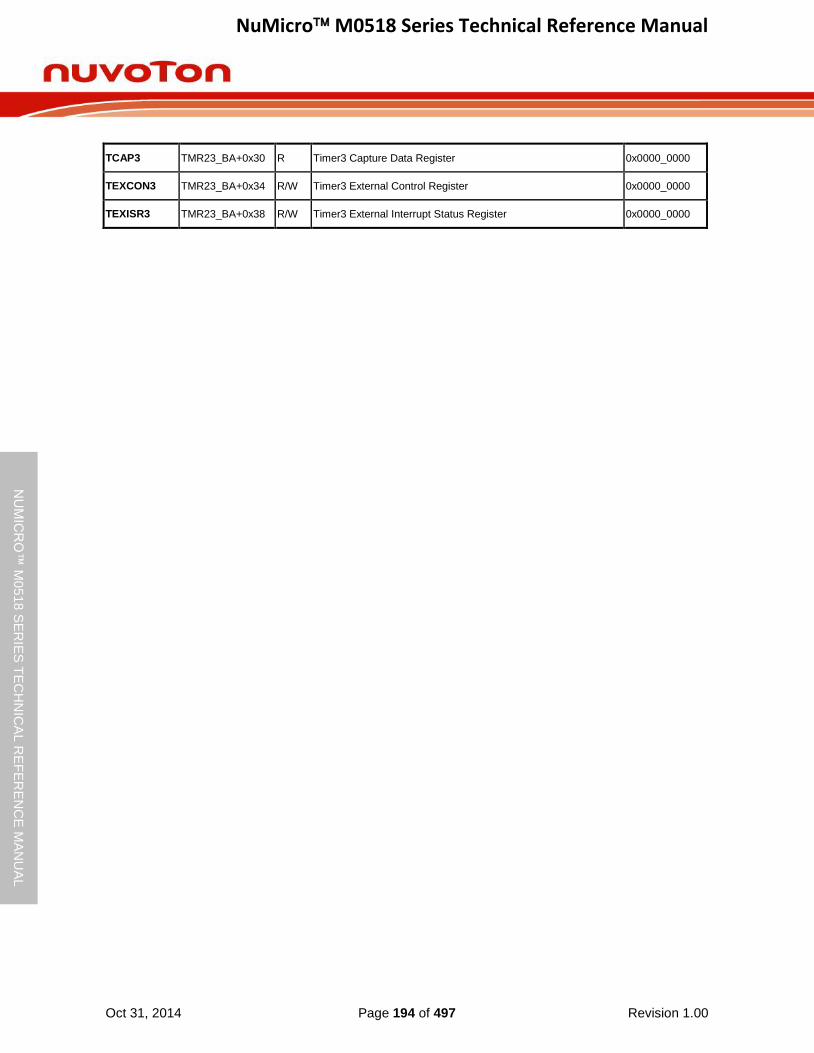
NuMicro M0518 Series Technical Reference Manual
Oct 31, 2014 Page 194 of 497 Revision 1.00
NU
MIC
RO
™ M
0518
SE
RIE
S T
EC
HN
ICA
L R
EF
ER
EN
CE
MA
NU
AL
TCAP3 TMR23_BA+0x30 R Timer3 Capture Data Register 0x0000_0000
TEXCON3 TMR23_BA+0x34 R/W Timer3 External Control Register 0x0000_0000
TEXISR3 TMR23_BA+0x38 R/W Timer3 External Interrupt Status Register 0x0000_0000
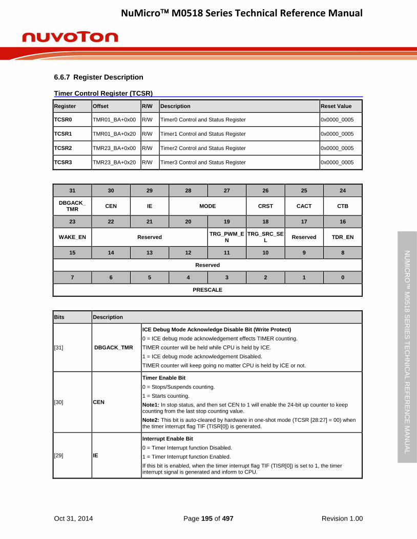
NuMicro M0518 Series Technical Reference Manual
Oct 31, 2014 Page 195 of 497 Revision 1.00
NU
MIC
RO
™ M
0518
SE
RIE
S T
EC
HN
ICA
L R
EF
ER
EN
CE
MA
NU
AL
6.6.7 Register Description
Timer Control Register (TCSR)
Register Offset R/W Description Reset Value
TCSR0 TMR01_BA+0x00 R/W Timer0 Control and Status Register 0x0000_0005
TCSR1 TMR01_BA+0x20 R/W Timer1 Control and Status Register 0x0000_0005
TCSR2 TMR23_BA+0x00 R/W Timer2 Control and Status Register 0x0000_0005
TCSR3 TMR23_BA+0x20 R/W Timer3 Control and Status Register 0x0000_0005
31 30 29 28 27 26 25 24
DBGACK_ TMR
CEN IE MODE CRST CACT CTB
23 22 21 20 19 18 17 16
WAKE_EN Reserved TRG_PWM_E
N TRG_SRC_SE
L Reserved TDR_EN
15 14 13 12 11 10 9 8
Reserved
7 6 5 4 3 2 1 0
PRESCALE
Bits Description
[31] DBGACK_TMR
ICE Debug Mode Acknowledge Disable Bit (Write Protect)
0 = ICE debug mode acknowledgement effects TIMER counting.
TIMER counter will be held while CPU is held by ICE.
1 = ICE debug mode acknowledgement Disabled.
TIMER counter will keep going no matter CPU is held by ICE or not.
[30] CEN
Timer Enable Bit
0 = Stops/Suspends counting.
1 = Starts counting.
Note1: In stop status, and then set CEN to 1 will enable the 24-bit up counter to keep counting from the last stop counting value.
Note2: This bit is auto-cleared by hardware in one-shot mode (TCSR [28:27] = 00) when the timer interrupt flag TIF (TISR[0]) is generated.
[29] IE
Interrupt Enable Bit
0 = Timer Interrupt function Disabled.
1 = Timer Interrupt function Enabled.
If this bit is enabled, when the timer interrupt flag TIF (TISR[0]) is set to 1, the timer interrupt signal is generated and inform to CPU.
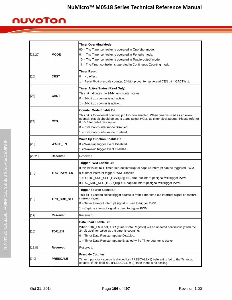
NuMicro M0518 Series Technical Reference Manual
Oct 31, 2014 Page 196 of 497 Revision 1.00
NU
MIC
RO
™ M
0518
SE
RIE
S T
EC
HN
ICA
L R
EF
ER
EN
CE
MA
NU
AL
[28:27] MODE
Timer Operating Mode
00 = The Timer controller is operated in One-shot mode.
01 = The Timer controller is operated in Periodic mode.
10 = The Timer controller is operated in Toggle-output mode.
11 = The Timer controller is operated in Continuous Counting mode.
[26] CRST
Timer Reset
0 = No effect.
1 = Reset 8-bit prescale counter, 24-bit up counter value and CEN bit if CACT is 1.
[25] CACT
Timer Active Status (Read Only)
This bit indicates the 24-bit up counter status.
0 = 24-bit up counter is not active.
1 = 24-bit up counter is active.
[24] CTB
Counter Mode Enable Bit
This bit is for external counting pin function enabled. When timer is used as an event counter, this bit should be set to 1 and select HCLK as timer clock source. Please refer to 6.6.5.6 for detail description.
0 = External counter mode Disabled.
1 = External counter mode Enabled.
[23] WAKE_EN
Wake Up Function Enable Bit
0 = Wake-up trigger event Disabled.
1 = Wake-up trigger event Enabled.
[22:20] Reserved Reserved.
[19] TRG_PWM_EN
Trigger PWM Enable Bit
If this bit is set to 1, timer time-out interrupt or capture interrupt can be triggered PWM.
0 = Timer interrupt trigger PWM Disabled.
1 = If TRG_SRC_SEL (TCSR[18]) = 0, time-out interrupt signal will trigger PWM.
If TRG_SRC_SEL (TCSR[18]) = 1, capture interrupt signal will trigger PWM.
[18] TRG_SRC_SEL
Trigger Source Select Bit
This bit is used to select trigger source is from Timer time-out interrupt signal or capture interrupt signal.
0 = Timer time-out interrupt signal is used to trigger PWM.
1 = Capture interrupt signal is used to trigger PWM.
[17] Reserved Reserved.
[16] TDR_EN
Data Load Enable Bit
When TDR_EN is set, TDR (Timer Data Register) will be updated continuously with the 24-bit up-timer value as the timer is counting.
0 = Timer Data Register update Disabled.
1 = Timer Data Register update Enabled while Timer counter is active.
[15:8] Reserved Reserved.
[7:0] PRESCALE
Prescale Counter
Timer input clock source is divided by (PRESCALE+1) before it is fed to the Timer up counter. If this field is 0 (PRESCALE = 0), then there is no scaling.
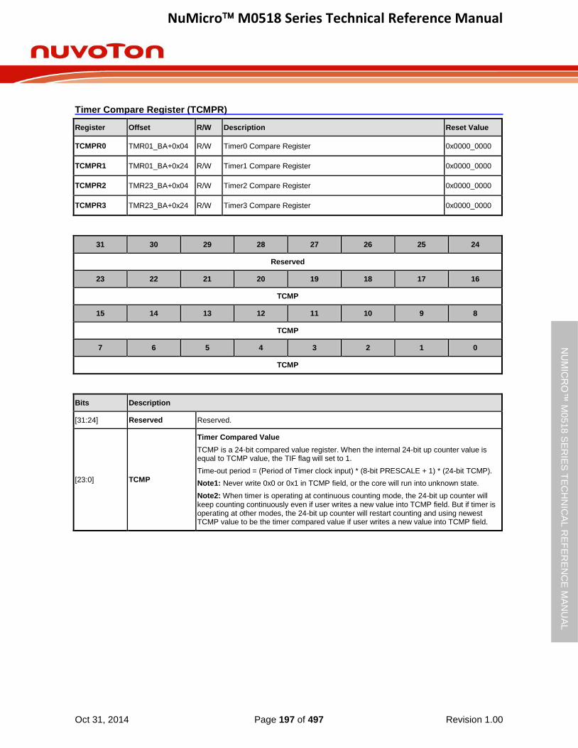
NuMicro M0518 Series Technical Reference Manual
Oct 31, 2014 Page 197 of 497 Revision 1.00
NU
MIC
RO
™ M
0518
SE
RIE
S T
EC
HN
ICA
L R
EF
ER
EN
CE
MA
NU
AL
Timer Compare Register (TCMPR)
Register Offset R/W Description Reset Value
TCMPR0 TMR01_BA+0x04 R/W Timer0 Compare Register 0x0000_0000
TCMPR1 TMR01_BA+0x24 R/W Timer1 Compare Register 0x0000_0000
TCMPR2 TMR23_BA+0x04 R/W Timer2 Compare Register 0x0000_0000
TCMPR3 TMR23_BA+0x24 R/W Timer3 Compare Register 0x0000_0000
31 30 29 28 27 26 25 24
Reserved
23 22 21 20 19 18 17 16
TCMP
15 14 13 12 11 10 9 8
TCMP
7 6 5 4 3 2 1 0
TCMP
Bits Description
[31:24] Reserved Reserved.
[23:0] TCMP
Timer Compared Value
TCMP is a 24-bit compared value register. When the internal 24-bit up counter value is equal to TCMP value, the TIF flag will set to 1.
Time-out period = (Period of Timer clock input) * (8-bit PRESCALE + 1) * (24-bit TCMP).
Note1: Never write 0x0 or 0x1 in TCMP field, or the core will run into unknown state.
Note2: When timer is operating at continuous counting mode, the 24-bit up counter will keep counting continuously even if user writes a new value into TCMP field. But if timer is operating at other modes, the 24-bit up counter will restart counting and using newest TCMP value to be the timer compared value if user writes a new value into TCMP field.
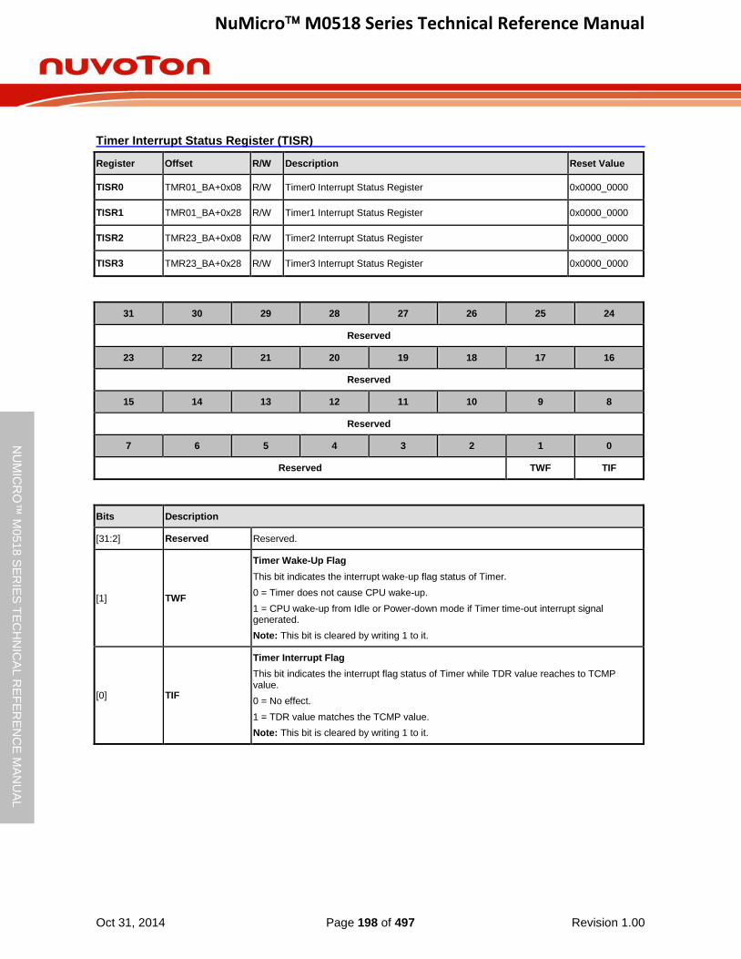
NuMicro M0518 Series Technical Reference Manual
Oct 31, 2014 Page 198 of 497 Revision 1.00
NU
MIC
RO
™ M
0518
SE
RIE
S T
EC
HN
ICA
L R
EF
ER
EN
CE
MA
NU
AL
Timer Interrupt Status Register (TISR)
Register Offset R/W Description Reset Value
TISR0 TMR01_BA+0x08 R/W Timer0 Interrupt Status Register 0x0000_0000
TISR1 TMR01_BA+0x28 R/W Timer1 Interrupt Status Register 0x0000_0000
TISR2 TMR23_BA+0x08 R/W Timer2 Interrupt Status Register 0x0000_0000
TISR3 TMR23_BA+0x28 R/W Timer3 Interrupt Status Register 0x0000_0000
31 30 29 28 27 26 25 24
Reserved
23 22 21 20 19 18 17 16
Reserved
15 14 13 12 11 10 9 8
Reserved
7 6 5 4 3 2 1 0
Reserved TWF TIF
Bits Description
[31:2] Reserved Reserved.
[1] TWF
Timer Wake-Up Flag
This bit indicates the interrupt wake-up flag status of Timer.
0 = Timer does not cause CPU wake-up.
1 = CPU wake-up from Idle or Power-down mode if Timer time-out interrupt signal generated.
Note: This bit is cleared by writing 1 to it.
[0] TIF
Timer Interrupt Flag
This bit indicates the interrupt flag status of Timer while TDR value reaches to TCMP value.
0 = No effect.
1 = TDR value matches the TCMP value.
Note: This bit is cleared by writing 1 to it.

NuMicro M0518 Series Technical Reference Manual
Oct 31, 2014 Page 199 of 497 Revision 1.00
NU
MIC
RO
™ M
0518
SE
RIE
S T
EC
HN
ICA
L R
EF
ER
EN
CE
MA
NU
AL
Timer Data Register (TDR)
Register Offset R/W Description Reset Value
TDR0 TMR01_BA+0x0C R Timer0 Data Register 0x0000_0000
TDR1 TMR01_BA+0x2C R Timer1 Data Register 0x0000_0000
TDR2 TMR23_BA+0x0C R Timer2 Data Register 0x0000_0000
TDR3 TMR23_BA+0x2C R Timer3 Data Register 0x0000_0000
31 30 29 28 27 26 25 24
Reserved
23 22 21 20 19 18 17 16
TDR
15 14 13 12 11 10 9 8
TDR
7 6 5 4 3 2 1 0
TDR
Bits Description
[31:24] Reserved Reserved.
[23:0] TDR
Timer Data Register
If TDR_EN (TCSR[16]) is set to 1, TDR register will be updated continuously to monitor 24-bit up counter value.
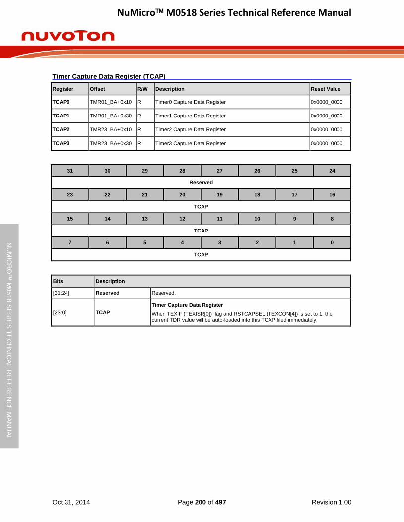
NuMicro M0518 Series Technical Reference Manual
Oct 31, 2014 Page 200 of 497 Revision 1.00
NU
MIC
RO
™ M
0518
SE
RIE
S T
EC
HN
ICA
L R
EF
ER
EN
CE
MA
NU
AL
Timer Capture Data Register (TCAP)
Register Offset R/W Description Reset Value
TCAP0 TMR01_BA+0x10 R Timer0 Capture Data Register 0x0000_0000
TCAP1 TMR01_BA+0x30 R Timer1 Capture Data Register 0x0000_0000
TCAP2 TMR23_BA+0x10 R Timer2 Capture Data Register 0x0000_0000
TCAP3 TMR23_BA+0x30 R Timer3 Capture Data Register 0x0000_0000
31 30 29 28 27 26 25 24
Reserved
23 22 21 20 19 18 17 16
TCAP
15 14 13 12 11 10 9 8
TCAP
7 6 5 4 3 2 1 0
TCAP
Bits Description
[31:24] Reserved Reserved.
[23:0] TCAP
Timer Capture Data Register
When TEXIF (TEXISR[0]) flag and RSTCAPSEL (TEXCON[4]) is set to 1, the current TDR value will be auto-loaded into this TCAP filed immediately.

NuMicro M0518 Series Technical Reference Manual
Oct 31, 2014 Page 201 of 497 Revision 1.00
NU
MIC
RO
™ M
0518
SE
RIE
S T
EC
HN
ICA
L R
EF
ER
EN
CE
MA
NU
AL
Timer External Control Register (TEXCON)
Register Offset R/W Description Reset Value
TEXCON0 TMR01_BA+0x14 R/W Timer0 External Control Register 0x0000_0000
TEXCON1 TMR01_BA+0x34 R/W Timer1 External Control Register 0x0000_0000
TEXCON2 TMR23_BA+0x14 R/W Timer2 External Control Register 0x0000_0000
TEXCON3 TMR23_BA+0x34 R/W Timer3 External Control Register 0x0000_0000
31 30 29 28 27 26 25 24
Reserved
23 22 21 20 19 18 17 16
Reserved
15 14 13 12 11 10 9 8
Reserved
7 6 5 4 3 2 1 0
TCDB TEXDB TEXIEN RSTCAPSEL TEXEN TEX_EDGE TX_PHASE
Bits Description
[31:8] Reserved Reserved.
[7] TCDB
Timer External Counter Input Pin De-Bounce Enable Bit
0 = TMx pin de-bounce Disabled.
1 = TMx pin de-bounce Enabled.
If this bit is enabled, the edge detection of TMx pin is detected with de-bounce circuit.
[6] TEXDB
Timer External Capture Input Pin De-Bounce Enable Bit
0 = TMx_EXT pin de-bounce Disabled.
1 = TMx_EXT pin de-bounce Enabled.
If this bit is enabled, the edge detection of TMx_EXT pin is detected with de-bounce circuit.
[5] TEXIEN
Timer External Capture Interrupt Enable Bit
0 = TMx_EXT pin detection Interrupt Disabled.
1 = TMx_EXT pin detection Interrupt Enabled.
If TEXIEN enabled, Timer will raise an external capture interrupt signal and inform to CPU while TEXIF flag is set to 1.
[4] RSTCAPSEL
Timer External Reset Counter / Timer External Capture Mode Selection
0 = Transition on TMx_EXT pin is using to save the TDR value into TCAP.(event capture function)
1 = Transition on TMx_EXT pin is using to reset the 24-bit up counter.(event reset counter function)
[3] TEXEN Timer External Pin Function Enable Bit
This bit enables the RSTCAPSEL function on the TMx_EXT pin.

NuMicro M0518 Series Technical Reference Manual
Oct 31, 2014 Page 202 of 497 Revision 1.00
NU
MIC
RO
™ M
0518
SE
RIE
S T
EC
HN
ICA
L R
EF
ER
EN
CE
MA
NU
AL
0 = RSTCAPSEL function of TMx_EXT pin will be ignored.
1 = RSTCAPSEL function of TMx_EXT pin is active.
[2:1] TEX_EDGE
Timer External Capture Pin Edge Detect Selection
00 = A 1 to 0 transition on TMx_EXT pin will be detected.
01 = A 0 to 1 transition on TMx_EXT pin will be detected.
10 = Either 1 to 0 or 0 to 1 transition on TMx_EXT pin will be detected.
11 = Reserved.
[0] TX_PHASE
Timer External Count Pin Phase Detect Selection
This bit indicates the detection phase of TMx_EXT pin.
0 = A falling edge of TMx_EXT pin will be counted.
1 = A rising edge of TMx_EXT pin will be counted.

NuMicro M0518 Series Technical Reference Manual
Oct 31, 2014 Page 203 of 497 Revision 1.00
NU
MIC
RO
™ M
0518
SE
RIE
S T
EC
HN
ICA
L R
EF
ER
EN
CE
MA
NU
AL
Timer External Interrupt Status Register (TEXISR)
Register Offset R/W Description Reset Value
TEXISR0 TMR01_BA+0x18 R/W Timer0 External Interrupt Status Register 0x0000_0000
TEXISR1 TMR01_BA+0x38 R/W Timer1 External Interrupt Status Register 0x0000_0000
TEXISR2 TMR23_BA+0x18 R/W Timer2 External Interrupt Status Register 0x0000_0000
TEXISR3 TMR23_BA+0x38 R/W Timer3 External Interrupt Status Register 0x0000_0000
31 30 29 28 27 26 25 24
Reserved
23 22 21 20 19 18 17 16
Reserved
15 14 13 12 11 10 9 8
Reserved
7 6 5 4 3 2 1 0
Reserved TEXIF
Bits Description
[31:1] Reserved Reserved.
[0] TEXIF
Timer External Capture Interrupt Flag
This bit indicates the external capture interrupt flag status.
When TEXEN (TEXCON[3]) enabled, TMx_EXT pin selected as external capture function, and a transition on TMx_EXT pin matched the TEX_EDGE (TEXCON[2:1]) setting, this flag will set to 1 by hardware.
0 = TMx_EXT pin interrupt did not occur.
1 = TMx_EXT pin interrupt occurred.
Note: This bit is cleared by writing 1 to it.
NuMicro M0518 Series Technical Reference Manual
Oct 31, 2014 Page 204 of 497 Revision 1.00
NU
MIC
RO
™ M
0518
SE
RIE
S T
EC
HN
ICA
L R
EF
ER
EN
CE
MA
NU
AL
6.7 PWM Generator and Capture Timer (PWM)
6.7.1 Overview
The M0518 provides two PWM generators - PWM0 and PWM1 as shown in Figure 6-23. Each
PWM supports 6 channels of PWM output or input capture. There is a 12-bit prescaler to support flexible clock to the 16-bit PWM counter with 16-bit comparator. The PWM counter supports up, down and up-down counter types. PWM uses the comparator compared with counter to generate events. These events are used to generate PWM pulse, interrupt and trigger signal for ADC to start conversion.
The PWM generator supports two standard PWM output modes: Independent mode and Complementary mode, which have difference architecture. In Complementary mode, there are two comparators to generate various PWM pulse with 12-bit dead-time generator. For PWM output control unit, it supports polarity output, independent pin mask, tri-state output enable and brake functions.
The PWM generator also supports input capture function to latch PWM counter value to the corresponding register when input channel has a rising transition, falling transition or both transition is happened.
6.7.2 Features
6.7.2.1 PWM function features
Supports maximum clock frequency up to100 MHz
Supports up to two PWM modules, each module provides 6 output channels
Supports independent mode for PWM output/Capture input channel
Supports complementary mode for 3 complementary paired PWM output channel
Dead-time insertion with 12-bit resolution
Two compared values during one period
Supports 12-bit pre-scalar from 1 to 4096
Supports 16-bit resolution PWM counter, each module provides 3 PWM counters
Up, down and up/down counter operation type
Supports mask function and tri-state enable for each PWM pin
Supports brake function
Brake source from pin and system safety events (clock failed, Brown-out detection and CPU lockup)
Noise filter for brake source from pin
Edge detect brake source to control brake state until brake interrupt cleared
Level detect brake source to auto recover function after brake condition removed
Supports interrupt on the following events:
PWM counter match zero, period value or compared value
Brake condition happened
Supports trigger ADC on the following events:
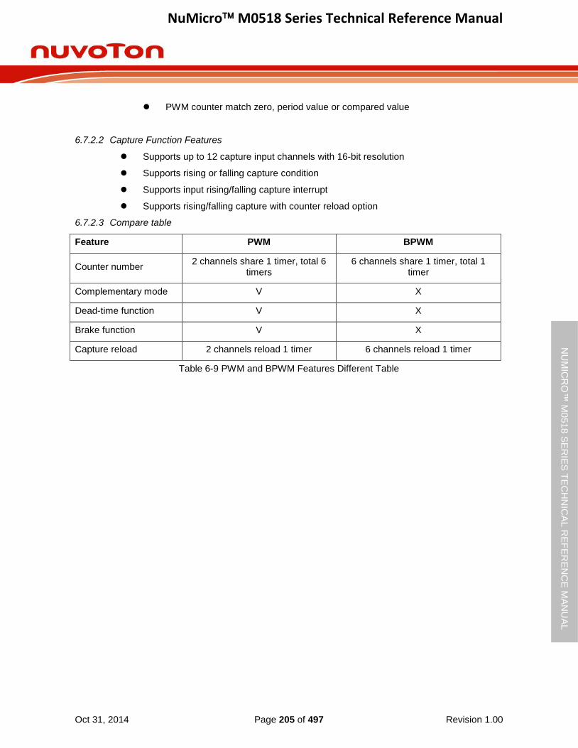
NuMicro M0518 Series Technical Reference Manual
Oct 31, 2014 Page 205 of 497 Revision 1.00
NU
MIC
RO
™ M
0518
SE
RIE
S T
EC
HN
ICA
L R
EF
ER
EN
CE
MA
NU
AL
PWM counter match zero, period value or compared value
6.7.2.2 Capture Function Features
Supports up to 12 capture input channels with 16-bit resolution
Supports rising or falling capture condition
Supports input rising/falling capture interrupt
Supports rising/falling capture with counter reload option
6.7.2.3 Compare table
Feature PWM BPWM
Counter number 2 channels share 1 timer, total 6
timers 6 channels share 1 timer, total 1
timer
Complementary mode V X
Dead-time function V X
Brake function V X
Capture reload 2 channels reload 1 timer 6 channels reload 1 timer
Table 6-9 PWM and BPWM Features Different Table
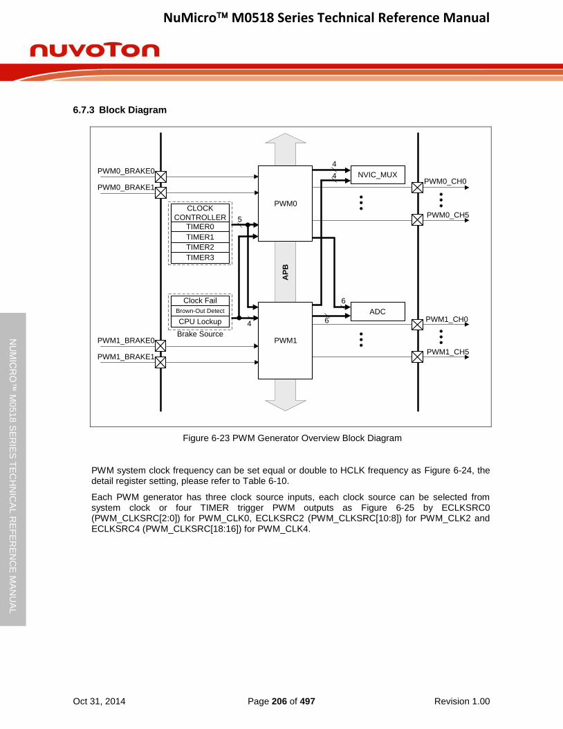
NuMicro M0518 Series Technical Reference Manual
Oct 31, 2014 Page 206 of 497 Revision 1.00
NU
MIC
RO
™ M
0518
SE
RIE
S T
EC
HN
ICA
L R
EF
ER
EN
CE
MA
NU
AL
6.7.3 Block Diagram
AP
B
PWM0
PWM0_BRAKE0
PWM0_BRAKE1
SYNC_IN
PWM1_BRAKE0
PWM1_BRAKE1
TIMER0
ADC
CLOCK
CONTROLLER 5
PWM1
TIMER1
TIMER2
TIMER3
PWM0_CH0
PWM0_CH5
4
4 NVIC_MUX
6
6
PWM1_CH5
PWM1_CH0
Clock Fail
Brown-Out Detect
CPU Lockup
Brake Source
4
Figure 6-23 PWM Generator Overview Block Diagram
PWM system clock frequency can be set equal or double to HCLK frequency as Figure 6-24, the detail register setting, please refer to Table 6-10.
Each PWM generator has three clock source inputs, each clock source can be selected from system clock or four TIMER trigger PWM outputs as Figure 6-25 by ECLKSRC0 (PWM_CLKSRC[2:0]) for PWM_CLK0, ECLKSRC2 (PWM_CLKSRC[10:8]) for PWM_CLK2 and ECLKSRC4 (PWM_CLKSRC[18:16]) for PWM_CLK4.

NuMicro M0518 Series Technical Reference Manual
Oct 31, 2014 Page 207 of 497 Revision 1.00
NU
MIC
RO
™ M
0518
SE
RIE
S T
EC
HN
ICA
L R
EF
ER
EN
CE
MA
NU
AL
HCLK_S (CLKSEL0[2:0])
1/(HCLK_N+1) HCLK0
1
0
1
PWM0
system clock
PWM1
system clock
PCLK
PCLK
PWM1_S (CLKSEL3[17])
PWM0_S (CLKSEL3[16])
PWM0_EN (APBCLK1[16])
PWM1_EN (APBCLK1[17])
HCLK_N (CLKDIV[3:0])
0
1
2
3
7
4~24MHzReservedPLLFOUT
10kHz22.1184MHz
Figure 6-24 PWM System Clock Source Control
Table 6-10 PWM System Clock Source Control Registers Setting Table
PWM0 system clock
PWM1 system clock
TIMER0
TIMER1
TIMER2TIMER3
0
1
2
34
TIMER0
TIMER1
TIMER2TIMER3
0
1
2
34
ECLKSRC0 (PWM_CLKSRC[2:0])
ECLKSRC0 (PWM_CLKSRC[2:0])
PWM0_CLK0
PWM1_CLK0
Figure 6-25 PWM Clock Source Control
Figure 6-26and Figure 6-27 illustrate the architecture of PWM Independent mode and Complementary mode. Regardless of Independent mode or Complementary mode, paired channels’ (PWM_CH0 and PWM_CH1, PWM_CH2 and PWM_CH3, PWM_CH4 and PWM_CH5) share the same counter. When the counter counts to 0, PERIOD (PWM_PERIODn[15:0]) or equal to comparator, events will be generated. These events are passed to the corresponding generators to generate PWM pulse, interrupt signal and trigger signal for ADC to start conversion. Output control is used to changing PWM pulse output state; brake function in output control also generates interrupt events. In Complementary mode, even channel use odd channel comparator to generate events.
PWM System Clock/HCLK
Frequency Ratio
HCLK_S
(CLKSEL0[2:0])
HCLK_N
(CLKDIV[3:0])
PWMn_S (CLKSEL3[X]),
(N, X) Denotes (0, 16) Or (1, 17)
1/1 Don’t care Don’t care 1
2/1 2 1 0

NuMicro M0518 Series Technical Reference Manual
Oct 31, 2014 Page 208 of 497 Revision 1.00
NU
MIC
RO
™ M
0518
SE
RIE
S T
EC
HN
ICA
L R
EF
ER
EN
CE
MA
NU
AL
Prescaler0
12bits
Interrupt
Generator
Trigger
Generator
NVIC_MUX
ADC
PWM0_CH0
Prescaler2
12bits
Prescaler4
12bits
Pulse
Generator0
Output
Control0
Pulse
Generator1
Output
Control1
PWM0_CH1
PWM0_CH2Pulse
Generator2
Output
Control2
Pulse
Generator3
Output
Control3
PWM0_CH3
PWM0_CH4Pulse
Generator4
Output
Control4
Pulse
Generator5
Output
Control5
PWM0_CH5
PWM0_BRAKE0
PWM0_BRAKE1
PWM0_CLK0 PWM0_BRAKE0PWM0_BRAKE1
PWM0_BRAKE0PWM0_BRAKE1
PWM0_BRAKE0PWM0_BRAKE1
PWM0_BRAKE0PWM0_BRAKE1
PWM0_BRAKE0PWM0_BRAKE1
PWM0_BRAKE0PWM0_BRAKE1
i
i
i
i
i
Trigger events
Interrupt events
t
i
i
PWM0_CLK2
PWM0_CLK4
16
16
16Comparator1
Comparator0
Counter0_1
a
a
a
16
16
16Comparator3
Comparator2
Counter2_3
a
a
a
16
16
16Comparator5
Comparator4
Counter4_5
a
a
a
a
it
denotes interrupt events
denotes trigger events
denotes interrupt, trigger and pulse generate events
Note:
Figure 6-26 PWM Independent Mode Architecture Diagram

NuMicro M0518 Series Technical Reference Manual
Oct 31, 2014 Page 209 of 497 Revision 1.00
NU
MIC
RO
™ M
0518
SE
RIE
S T
EC
HN
ICA
L R
EF
ER
EN
CE
MA
NU
AL
Prescaler0
12bits
Interrupt
Generator
Trigger
Generator
NVIC_MUX
ADC
PWM0_CH0
Prescaler2
12bits
Prescaler4
12bits
Pulse
Generator0
Output
Control0
PWM0_CH1
PWM0_CH2
Pulse
Generator2
Output
Control2
PWM0_CH3
PWM0_CH4
Pulse
Generator4
Output
Control4
PWM0_CH5
PWM0_BRAKE0
PWM0_BRAKE1
PWM0_CLK0
PWM0_BRAKE0PWM0_BRAKE1
PWM0_BRAKE0PWM0_BRAKE1
PWM0_BRAKE0PWM0_BRAKE1
i
i
i
Trigger events
Interrupt events
t
i
PWM0_CLK2
PWM0_CLK4
16
16
16Comparator1
Comparator0
Counter0_1
a
a
a
16
16
16Comparator3
Comparator2
Counter2_3
a
a
a
16
16
16Comparator5
Comparator4
Counter4_5
a
a
a
a
it
denotes interrupt events
denotes trigger events
denotes interrupt, trigger and pulse generate events
Note:
Figure 6-27 PWM Complementary Mode Architecture Diagram
6.7.4 Basic Configuration
The PWM pin function is configured in GPA_MFP register, PWM_BRAKE0 and PWM_BRAKE1 pin functions are configured in GPB_MFP and GPC_MFP registers.
The PWM clock can be enabled in APBCLK1[17:16]. The PWM clock source is selected by CLKSEL3[17:16].
6.7.5 Functional Description
6.7.5.1 PWM Prescaler
The PWM prescaler is used to divide clock source, prescaler counting CLKPSC +1 times, PWM counter only count once. CLKPSC (Clock Pre-scale Register) is set by CLKPSC (PWM_CLKPSCn[11:0], n denotes 0, 2, 4). Figure 6-28 shows an example of PWM channel 0 CLKPSC waveform.
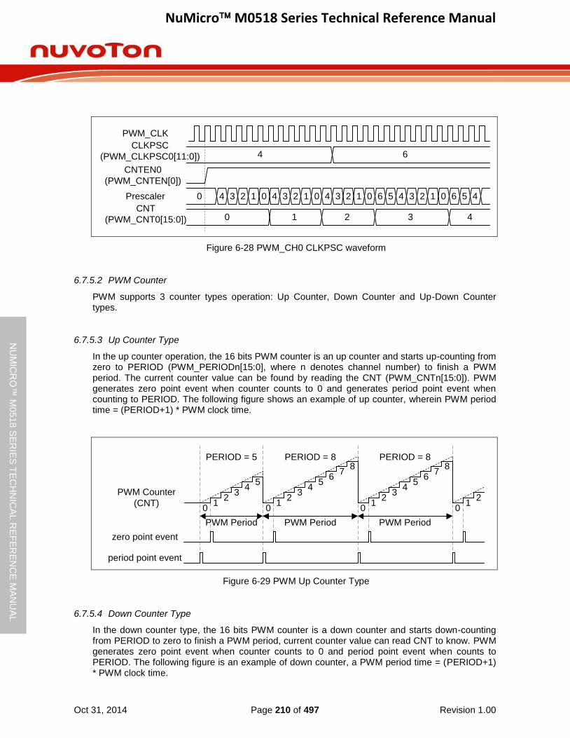
NuMicro M0518 Series Technical Reference Manual
Oct 31, 2014 Page 210 of 497 Revision 1.00
NU
MIC
RO
™ M
0518
SE
RIE
S T
EC
HN
ICA
L R
EF
ER
EN
CE
MA
NU
AL
0 1CNT
(PWM_CNT0[15:0])
4Prescaler
CLKPSC
(PWM_CLKPSC0[11:0])
3 2 1 0
3
CNTEN0
(PWM_CNTEN[0])
4 3 2 1 0 4 3 2 1 0 5 4 3 2 16 00
4 6
2 4
5 46
PWM_CLK
Figure 6-28 PWM_CH0 CLKPSC waveform
6.7.5.2 PWM Counter
PWM supports 3 counter types operation: Up Counter, Down Counter and Up-Down Counter types.
6.7.5.3 Up Counter Type
In the up counter operation, the 16 bits PWM counter is an up counter and starts up-counting from zero to PERIOD (PWM_PERIODn[15:0], where n denotes channel number) to finish a PWM period. The current counter value can be found by reading the CNT (PWM_CNTn[15:0]). PWM generates zero point event when counter counts to 0 and generates period point event when counting to PERIOD. The following figure shows an example of up counter, wherein PWM period time = (PERIOD+1) * PWM clock time.
01
23
45
PWM Counter
(CNT)0
12
34
56
78
01
23
45
67
8
01
2
PWM Period PWM Period
PERIOD = 5 PERIOD = 8
PWM Period
PERIOD = 8
zero point event
period point event
Figure 6-29 PWM Up Counter Type
6.7.5.4 Down Counter Type
In the down counter type, the 16 bits PWM counter is a down counter and starts down-counting from PERIOD to zero to finish a PWM period, current counter value can read CNT to know. PWM generates zero point event when counter counts to 0 and period point event when counts to PERIOD. The following figure is an example of down counter, a PWM period time = (PERIOD+1) * PWM clock time.
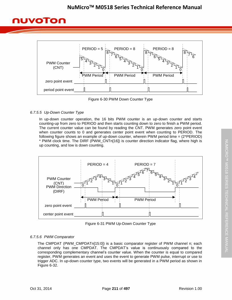
NuMicro M0518 Series Technical Reference Manual
Oct 31, 2014 Page 211 of 497 Revision 1.00
NU
MIC
RO
™ M
0518
SE
RIE
S T
EC
HN
ICA
L R
EF
ER
EN
CE
MA
NU
AL
01
23
45
01
23
45
67
8
01
23
45
67
86
78
PWM Counter
(CNT)
PWM Period PWM Period PWM Period
PERIOD = 5 PERIOD = 8 PERIOD = 8
zero point event
period point event
Figure 6-30 PWM Down Counter Type
6.7.5.5 Up-Down Counter Type
In up-down counter operation, the 16 bits PWM counter is an up-down counter and starts counting-up from zero to PERIOD and then starts counting down to zero to finish a PWM period. The current counter value can be found by reading the CNT. PWM generates zero point event when counter counts to 0 and generates center point event when counting to PERIOD. The following figure shows an example of up-down counter, wherein PWM period time = (2*PERIOD) * PWM clock time. The DIRF (PWM_CNTn[16]) is counter direction indicator flag, where high is up counting, and low is down counting.
PWM Direction
(DIRF)
PWM Counter
(CNT)0
12
34
31
20
12
34
31
20
56
76
45
12
34
PWM Period
PERIOD = 4 PERIOD = 7
PWM Period
zero point event
center point event
Figure 6-31 PWM Up-Down Counter Type
6.7.5.6 PWM Comparator
The CMPDAT (PWM_CMPDATn[15:0]) is a basic comparator register of PWM channel n; each channel only has one CMPDAT. The CMPDAT’s value is continuously compared to the corresponding complementary channel’s counter value. When the counter is equal to compared register, PWM generates an event and uses the event to generate PWM pulse, interrupt or use to trigger ADC. In up-down counter type, two events will be generated in a PWM period as shown in Figure 6-32.
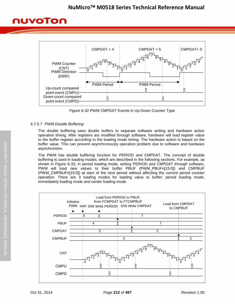
NuMicro M0518 Series Technical Reference Manual
Oct 31, 2014 Page 212 of 497 Revision 1.00
NU
MIC
RO
™ M
0518
SE
RIE
S T
EC
HN
ICA
L R
EF
ER
EN
CE
MA
NU
AL
PWM Direction
(DIRF)
PWM Counter
(CNT)0
12
34
31
20
12
34
31
20
56
76
45
12
34
PWM Period
CMPDAT = 4 CMPDAT = 5
PWM PeriodUp-count compared
point event (CMPU)Down-count compared
point event (CMPD)
CMPDAT= 0
Figure 6-32 PWM CMPDAT Events in Up-Down Counter Type
6.7.5.7 PWM Double Buffering
The double buffering uses double buffers to separate software writing and hardware action operation timing. After registers are modified through software, hardware will load register value to the buffer register according to the loading mode timing. The hardware action is based on the buffer value. This can prevent asynchronously operation problem due to software and hardware asynchronism.
The PWM has double buffering function for PERIOD and CMPDAT. The concept of double buffering is used in loading modes, which are described in the following sections. For example, as shown in Figure 6-33, in period loading mode, writing PERIOD and CMPDAT through software, PWM will load new values to their buffer PBUF (PWM_PBUFn[15:0]) and CMPBUF (PWM_CMPBUFn[15:0]) at start of the next period without affecting the current period counter operation. There are 3 loading modes for loading value to buffer: period loading mode, immediately loading mode and center loading mode.
CMPDAT
PERIOD
S/W Write PERIOD
CNT
4 7
3
start
Initialize
PWM
2
S/W Write CMPDAT
01
23
43
12
01
23
43
12
0
56
76
45
12
34
Load from PERIOD to PBUF,
from FCMPDAT to FTCMPBUF Load from CMPDAT
to CMPBUF
PBUF 4 7
CMPBUF 3 2
CMPU
CMPD
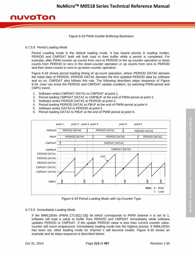
NuMicro M0518 Series Technical Reference Manual
Oct 31, 2014 Page 213 of 497 Revision 1.00
NU
MIC
RO
™ M
0518
SE
RIE
S T
EC
HN
ICA
L R
EF
ER
EN
CE
MA
NU
AL
Figure 6-33 PWM Double Buffering Illustration
6.7.5.8 Period Loading Mode
Period Loading mode is the default loading mode. It has lowest priority in loading modes. PERIOD and CMPDAT both will both load to their buffer while a period is completed. For example, after PWM counter up counts from zero to PERIOD in the up-counter operation or down counts from PERIOD to zero in the down-counter operation or up counts from zero to PERIOD and then down counts to zero in up-down counter operation.
Figure 6-34 shows period loading timing of up-count operation, where PERIOD DATA0 denotes the initial data of PERIOD, PERIOD DATA1 denotes the first updated PERIOD data by software and so on, CMPDAT also follows this rule. The following describes steps sequence of Figure 6-34. User can know the PERIOD and CMPDAT update condition, by watching PWM period and CMPU event.
1. Software writes CMPDAT DATA1 to CMPDAT at point 1. 2. Period loading CMPDAT DATA1 to CMPBUF at the end of PWM period at point 2. 3. Software writes PERIOD DATA1 to PERIOD at point 3. 4. Period loading PERIOD DATA1 to PBUF at the end of PWM period at point 4. 5. Software writes DATA2 to PERIOD at point 5. 6. Period loading DATA2 to PBUF at the end of PWM period at point 6.
CMPDAT DATA0
CMPU
CMPDAT DATA1
PERIOD DATA0
PERIOD DATA1
PERIOD DATA2
CNT
Write
Load
Note:
CMPDAT
PERIOD PERIOD DATA0 PERIOD DATA1
CMPDAT DATA1
PBUF PERIOD DATA0 PERIOD DATA1
CMPBUF CMPDAT DATA1
PERIOD DATA2
PERIOD DATA2
point 1 point 2 point 3 point 4 point 5 point 6
Figure 6-34 Period Loading Mode with Up-Counter Type
6.7.5.9 Immediately Loading Mode
If the IMMLDENn (PWM_CTL0[21:16]) bit which corresponds to PWM channel n is set to 1, software will load a value to buffer from PERIOD and CMPDAT immediately while software updates PERIOD or CMPDAT. If the update PERIOD value is less than current counter value, counter will count wraparound. Immediately loading mode has the highest priority. If IMMLDENn has been set, other loading mode for channel n will become invalid. Figure 6-35 shows an example and its steps sequence is described below.
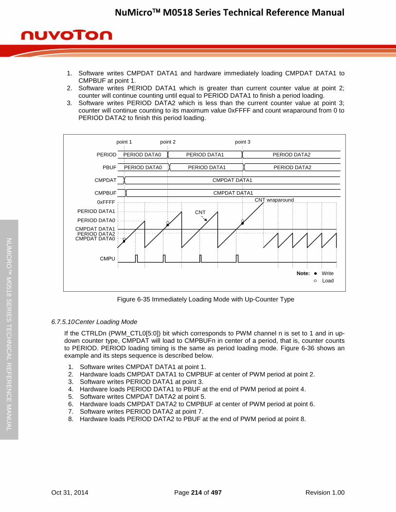
NuMicro M0518 Series Technical Reference Manual
Oct 31, 2014 Page 214 of 497 Revision 1.00
NU
MIC
RO
™ M
0518
SE
RIE
S T
EC
HN
ICA
L R
EF
ER
EN
CE
MA
NU
AL
1. Software writes CMPDAT DATA1 and hardware immediately loading CMPDAT DATA1 to CMPBUF at point 1.
2. Software writes PERIOD DATA1 which is greater than current counter value at point 2; counter will continue counting until equal to PERIOD DATA1 to finish a period loading.
3. Software writes PERIOD DATA2 which is less than the current counter value at point 3; counter will continue counting to its maximum value 0xFFFF and count wraparound from 0 to PERIOD DATA2 to finish this period loading.
CMPDAT DATA0
CMPU
CMPDAT DATA1
PERIOD DATA1
PERIOD DATA2
PERIOD DATA0
CNT
CNT wraparound0xFFFF
Write
Load
Note:
CMPDAT
PERIOD PERIOD DATA0 PERIOD DATA1
CMPDAT DATA1
PBUF PERIOD DATA0 PERIOD DATA1
CMPBUF CMPDAT DATA1
PERIOD DATA2
PERIOD DATA2
point 1 point 2 point 3
Figure 6-35 Immediately Loading Mode with Up-Counter Type
6.7.5.10 Center Loading Mode
If the CTRLDn (PWM_CTL0[5:0]) bit which corresponds to PWM channel n is set to 1 and in up-down counter type, CMPDAT will load to CMPBUFn in center of a period, that is, counter counts to PERIOD. PERIOD loading timing is the same as period loading mode. Figure 6-36 shows an example and its steps sequence is described below.
1. Software writes CMPDAT DATA1 at point 1. 2. Hardware loads CMPDAT DATA1 to CMPBUF at center of PWM period at point 2. 3. Software writes PERIOD DATA1 at point 3. 4. Hardware loads PERIOD DATA1 to PBUF at the end of PWM period at point 4. 5. Software writes CMPDAT DATA2 at point 5. 6. Hardware loads CMPDAT DATA2 to CMPBUF at center of PWM period at point 6. 7. Software writes PERIOD DATA2 at point 7. 8. Hardware loads PERIOD DATA2 to PBUF at the end of PWM period at point 8.

NuMicro M0518 Series Technical Reference Manual
Oct 31, 2014 Page 215 of 497 Revision 1.00
NU
MIC
RO
™ M
0518
SE
RIE
S T
EC
HN
ICA
L R
EF
ER
EN
CE
MA
NU
AL
CMPDAT DATA0
CMPU
CMPDAT DATA1
PERIOD DATA0
PERIOD DATA1
PERIOD DATA2
CNT
CMPDAT DATA2
CMPD
Write
Load
Note:
CMPDAT
PERIOD PERIOD DATA0 PERIOD DATA1
CMPDAT DATA1
PBUF PERIOD DATA0 PERIOD DATA1
CMPBUF CMPDAT DATA1
PERIOD DATA2
PERIOD DATA2
CMPDAT DATA0 CMPDAT DATA2
CMPDAT DATA2
point 1 point 2 point 3 point 4 point 5 point 6 point 7 point 8
Figure 6-36 Center Loading Mode with Up-Down-Counter Type
6.7.5.11 PWM Pulse Generator
PWM pulse generator uses counter and comparator events to generate PWM pulse. The events are: zero point, period point in up counter type and down counter type, center point in up-down counter type and counter equal to comparator point in three types. As to up-down counter type, there are two counter equal comparator points, one at up count another at down count. Besides, Complementary mode has two comparators compared with counter, and thus comparing equal points will become four in up-down counter type and two for up or down counter type.
Each event point can decide PWM waveform to do nothing (X), set Low (L), set High (H) or toggle (T) by setting PWM_WGCTL0 and PWM_WGCTL1 registers. Using these points can easily generate asymmetric PWM pulse or variant waveform as shown in Figure 6-37. In the figure, PWM is in Complementary mode, there are two comparators n and m to generate PWM pulse. n denotes even channel number 0, 2, 4, m denotes odd channel number 1, 3, 5. n and m channels are complementary paired. Complementary mode uses two channels (CH0 and CH1, CH2 and CH3, CH4 and CH5) as a pair of PWM outputs to generate complement paired waveforms. CMPU denotes CNT is equal to CMPDAT when counting up. CMPD denotes CNT is equal to CMPDAT when counting down.

NuMicro M0518 Series Technical Reference Manual
Oct 31, 2014 Page 216 of 497 Revision 1.00
NU
MIC
RO
™ M
0518
SE
RIE
S T
EC
HN
ICA
L R
EF
ER
EN
CE
MA
NU
AL
CNT
PWM period
Zero
CMPDATn
CMPDATm
Center
PWM period
CNT
PWM OUT
1
2
3
4
5
6
2. CMPUn = X
5. CMPDm = X
3. CMPUm = H
1. Zero = L
6. CMPDn = L
4. Center = X
Zero
CMPDATn
CMPDATm
Center
2. CMPUn = T
5. CMPDm = T
3. CMPUm = H
1. Zero = H
6. CMPDn = L
4. Center = L
Note: Note:
PWM OUT
1
2
3
4
5
6
Figure 6-37 PWM Pulse Generation
The generation events may be sometimes set to the same value, as the reason, events priority between different counter types are list below, up counter type (Table 6-11), down counter type (Table 6-12) and up-down counter type (Table 6-13).By using event priority, user can easily generate 0% to 100% duty pulse as shown in Figure 6-38.
0
1
2
3
4
3
2
1
0
1
2
3
4
3
2
1
0
CMPDAT = 0, 0% Duty
CMPDAT = 1, 25% Duty
CMPDAT = 2, 50% Duty
CMPDAT = 3, 75% Duty
CMPDAT = 4, 100% Duty
DIRF
PWM period PWM period
0
1
2
3
4
0
1
2
3
4
CMPDAT = 0, 0% Duty
CMPDAT = 1, 20% Duty
CMPDAT = 2, 40% Duty
CMPDAT = 3, 60% Duty
CMPDAT = 4, 80% Duty
CMPDAT > 4,100% Duty
CMPU = L
Zero = H
PWM period PWM period
CMPU = L
CMPD = H
Figure 6-38 PWM 0% to 100% Pulse Generation
Priority Up Event
1 (Highest) CNT = period (PERIOD)
2 CNT = CMPUm
3 CNT = CMPUn
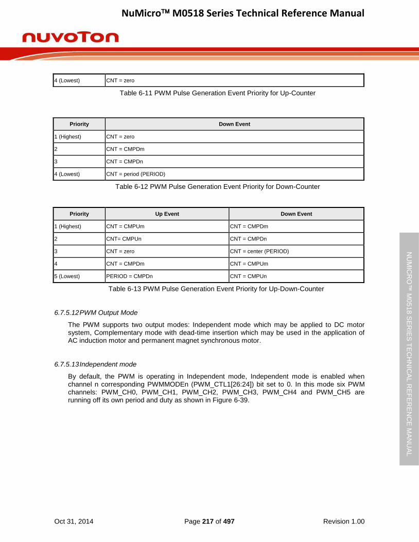
NuMicro M0518 Series Technical Reference Manual
Oct 31, 2014 Page 217 of 497 Revision 1.00
NU
MIC
RO
™ M
0518
SE
RIE
S T
EC
HN
ICA
L R
EF
ER
EN
CE
MA
NU
AL
Table 6-11 PWM Pulse Generation Event Priority for Up-Counter
Table 6-12 PWM Pulse Generation Event Priority for Down-Counter
Table 6-13 PWM Pulse Generation Event Priority for Up-Down-Counter
6.7.5.12 PWM Output Mode
The PWM supports two output modes: Independent mode which may be applied to DC motor system, Complementary mode with dead-time insertion which may be used in the application of AC induction motor and permanent magnet synchronous motor.
6.7.5.13 Independent mode
By default, the PWM is operating in Independent mode, Independent mode is enabled when channel n corresponding PWMMODEn (PWM_CTL1[26:24]) bit set to 0. In this mode six PWM channels: PWM_CH0, PWM_CH1, PWM_CH2, PWM_CH3, PWM_CH4 and PWM_CH5 are running off its own period and duty as shown in Figure 6-39.
4 (Lowest) CNT = zero
Priority Down Event
1 (Highest) CNT = zero
2 CNT = CMPDm
3 CNT = CMPDn
4 (Lowest) CNT = period (PERIOD)
Priority Up Event Down Event
1 (Highest) CNT = CMPUm CNT = CMPDm
2 CNT= CMPUn CNT = CMPDn
3 CNT = zero CNT = center (PERIOD)
4 CNT = CMPDm CNT = CMPUm
5 (Lowest) PERIOD = CMPDn CNT = CMPUn

NuMicro M0518 Series Technical Reference Manual
Oct 31, 2014 Page 218 of 497 Revision 1.00
NU
MIC
RO
™ M
0518
SE
RIE
S T
EC
HN
ICA
L R
EF
ER
EN
CE
MA
NU
AL
PWM_CH2
PWM_CH0
Setting: PWMMODE0 (PWM_CTL1[24]) = 0x0
PWM_CH1
PWM_CH3
PWM_CH4
PWM_CH5
Setting: PWMMODE2 (PWM_CTL1[25]) = 0x0
Setting: PWMMODE4 (PWM_CTL1[26]) = 0x0
Figure 6-39 PWM Independent Mode Waveform
6.7.5.14 Complementary mode
Complementary mode is enabled when the pair channel corresponding PWMMODEn (PWM_CTL1[26:24]) bit set to 1. In this mode there are 3 PWM generators utilized for Complementary mode, with total of 3 PWM output paired pins in this module. In Complimentary mode, the internal odd PWM signal must always be the complement of the corresponding even PWM signal. PWM_CH1 will be the complement of PWM_CH0. PWM_CH3 will be the complement of PWM_CH2 and PWM_CH5 will be the complement of PWM_CH4 as shown in Figure 6-40.
PWM_CH2
PWM_CH0
Setting: PWMMODE0 (PWM_CTL1[24]) = 0x1
PWM_CH1
PWM_CH3
PWM_CH4
PWM_CH5
Setting: PWMMODE2 (PWM_CTL1[25]) = 0x1
Setting: PWMMODE4 (PWM_CTL1[26]) = 0x1
Figure 6-40 PWM Complementary Mode Waveform
6.7.5.15 PWM Output Control
After PWM pulse generation, there are four to six steps to control the output of PWM channels. In Independent mode, there are Mask, Brake, Pin Polarity and Output Enable four steps as shown in Figure 6-41. In Complementary mode, it needs two more steps to precede these four steps,

NuMicro M0518 Series Technical Reference Manual
Oct 31, 2014 Page 219 of 497 Revision 1.00
NU
MIC
RO
™ M
0518
SE
RIE
S T
EC
HN
ICA
L R
EF
ER
EN
CE
MA
NU
AL
Complementary channels and Dead-Time Insertion as shown in Figure 6-42.
Mask Data n
1-bit
MSKDAT0
(PWM_MSK[0])
PINV0
(PWM_POLCTL[0])
POEN0
(PWM_POEN[0])
Brake
BRKAEVEN
(PWM_BRKCTLm[17:16])
PWM_BRKCTLm[15:0]
PWM_
WGCTL0
MSKEN0
(PWM_MSKEN[0])
PWM_CH0
Independent Mode 4 Steps
Mask Brake EnablePolarity
Figure 6-41 PWM_CH0 Output Control in Independent Mode
Dead Time
Insert0 12-bits
Dead Time
Insert0 12-bits
DTEN
(PWM_DTCTL0[16])
Independent Mode
Four Steps
Independent Mode
Four Steps
DTCNT
(PWM_DTCTL0[11:0])
PWM_
WGCTL0
Complementary
PWM_CH0
PWM_CH1
Dead Time Insertion
Figure 6-42 PWM_CH0 and PWM_CH1 Output Control in Complementary Mode
6.7.5.16 Dead-Time Insertion
In the complementary application, the complement channels may drive the external devices like power switches. The dead-time generator inserts a low level period called “dead-time” between complementary outputs to drive these devices safely and to prevent system or devices from the burn-out damage. Hence the dead-time control is a crucial mechansism to the proper operation of the complementary system. By setting corresponding channel n DTEN (PWM_DTCTLn[16]) bit to enable dead-time function and DTCNT (PWM_DTCTLn[11:0]) to control dead-time period, the dead-time can be calculated from the following formula:
Dead-time = (DTCNT[11:0]+1) * PWMx_CLK period
Figure 6-43 indicates the dead-time insertion for one pair of PWM signals.
Dead-time insertion clock source can be selected from prescaler output by setting DTCKSEL (PWM_DTCTLn[24]) to 1. By default, clock source is come from PWM_CLK, which is prescaler input. Please note that the PWM_DTCTLn is a write-protected register.
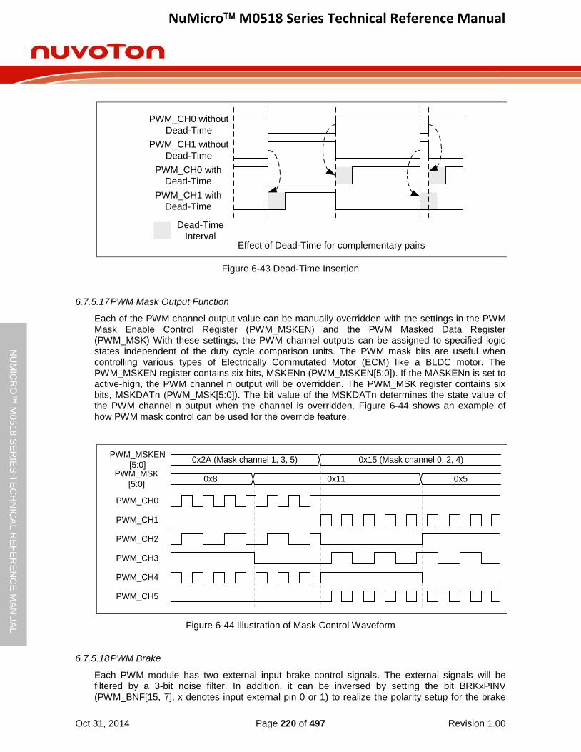
NuMicro M0518 Series Technical Reference Manual
Oct 31, 2014 Page 220 of 497 Revision 1.00
NU
MIC
RO
™ M
0518
SE
RIE
S T
EC
HN
ICA
L R
EF
ER
EN
CE
MA
NU
AL
PWM_CH0 without
Dead-Time
PWM_CH1 without
Dead-Time
PWM_CH0 with
Dead-Time
PWM_CH1 with
Dead-Time
Dead-Time
IntervalEffect of Dead-Time for complementary pairs
Figure 6-43 Dead-Time Insertion
6.7.5.17 PWM Mask Output Function
Each of the PWM channel output value can be manually overridden with the settings in the PWM Mask Enable Control Register (PWM_MSKEN) and the PWM Masked Data Register (PWM_MSK) With these settings, the PWM channel outputs can be assigned to specified logic states independent of the duty cycle comparison units. The PWM mask bits are useful when controlling various types of Electrically Commutated Motor (ECM) like a BLDC motor. The PWM_MSKEN register contains six bits, MSKENn (PWM_MSKEN[5:0]). If the MASKENn is set to active-high, the PWM channel n output will be overridden. The PWM_MSK register contains six bits, MSKDATn (PWM_MSK[5:0]). The bit value of the MSKDATn determines the state value of the PWM channel n output when the channel is overridden. Figure 6-44 shows an example of how PWM mask control can be used for the override feature.
PWM_CH2
PWM_CH0
PWM_MSK
[5:0]0x8 0x11 0x5
PWM_MSKEN
[5:0]
PWM_CH1
PWM_CH3
0x2A (Mask channel 1, 3, 5) 0x15 (Mask channel 0, 2, 4)
PWM_CH4
PWM_CH5
Figure 6-44 Illustration of Mask Control Waveform
6.7.5.18 PWM Brake
Each PWM module has two external input brake control signals. The external signals will be filtered by a 3-bit noise filter. In addition, it can be inversed by setting the bit BRKxPINV (PWM_BNF[15, 7], x denotes input external pin 0 or 1) to realize the polarity setup for the brake
NuMicro M0518 Series Technical Reference Manual
Oct 31, 2014 Page 221 of 497 Revision 1.00
NU
MIC
RO
™ M
0518
SE
RIE
S T
EC
HN
ICA
L R
EF
ER
EN
CE
MA
NU
AL
control signals. The noise filter sampling clock can be selected by setting bits BRKxFCS (PWM_BNF[11:9, 3:1]) to fit different noise properties. Moreover, by setting the bits BRKxFCNT (PWM_BNF[14:12, 6:4]), user can define by how many sampling clock cycles a filter will recognize the effective edge of the brake signal. Configuring the BRKxFEN (PWM_BNF[8, 0]) will enable the noise filter function. By default, it is disabled.
8 to
1 M
UX
HCLK
HCLK/2
HCLK/4
HCLK/8
HCLK/16
HCLK/32
HCLK/64
HCLK/128
BRKxFCS
(PWM_BNF[3:1] for BKP0)
(PWM_BNF[11:9] for BKP1)
Noise filter
counter 3-bits
BRKxFCNT
(PWM_BNF[6:4] for BKP0)
(PWM_BNF[14:12] for BKP1)
PWM_BRAKEx
BRKxPINV
(PWM_BNF[7] for BKP0)
(PWM_BNF[15] for BKP1)
01
Brake Source
Note: x denotes 0 or 1
0
1
2
3
4
5
6
7
BRKxFEN
(PWM_BNF[0] for BKP0)
(PWM_BNF[8] for BKP1)
Sampling Clock
3
3
Figure 6-45 Brake Noise Filter Block Diagram
Each complementary channel pair shares a PWM brake function, as shown in Figure 6-46. To control paired channels to output safety state, user can setup BRKAEVEN (PWM_BRKCTL0_1[17:16]) for even channels and BRKAODD (PWM_BRKCTL0_1[19:18]) for odd channels when the fault brake event happens. There are two brake detectors: Edge detector and Level detector. When the edge detector detects the brake signal and BRKEIENn_m (PWM_INTEN1[2:0]) is enabled, the brake function generates BRK_INT. This interrupt needs software to clear, and the BRKESTSn (PWM_INTSTS1[21:16]) brake state will keep until the next PWM period starts after the interrupt cleared. The brake function can also operate in another way through the level detector. Once the level detector detects the brake signal and the BRKLIENn_m (PWM_INTEN1[10:8]) is also enabled, the brake function will generate BRK_INT, but BRKLSTSn (PWM_INTSTS1[29:24]) brake state will auto recovery to normal output while level brake source recovery to high level and pass through “Low Level Detection” at the PWM waveform period when brake condition removed without clear interrupt.
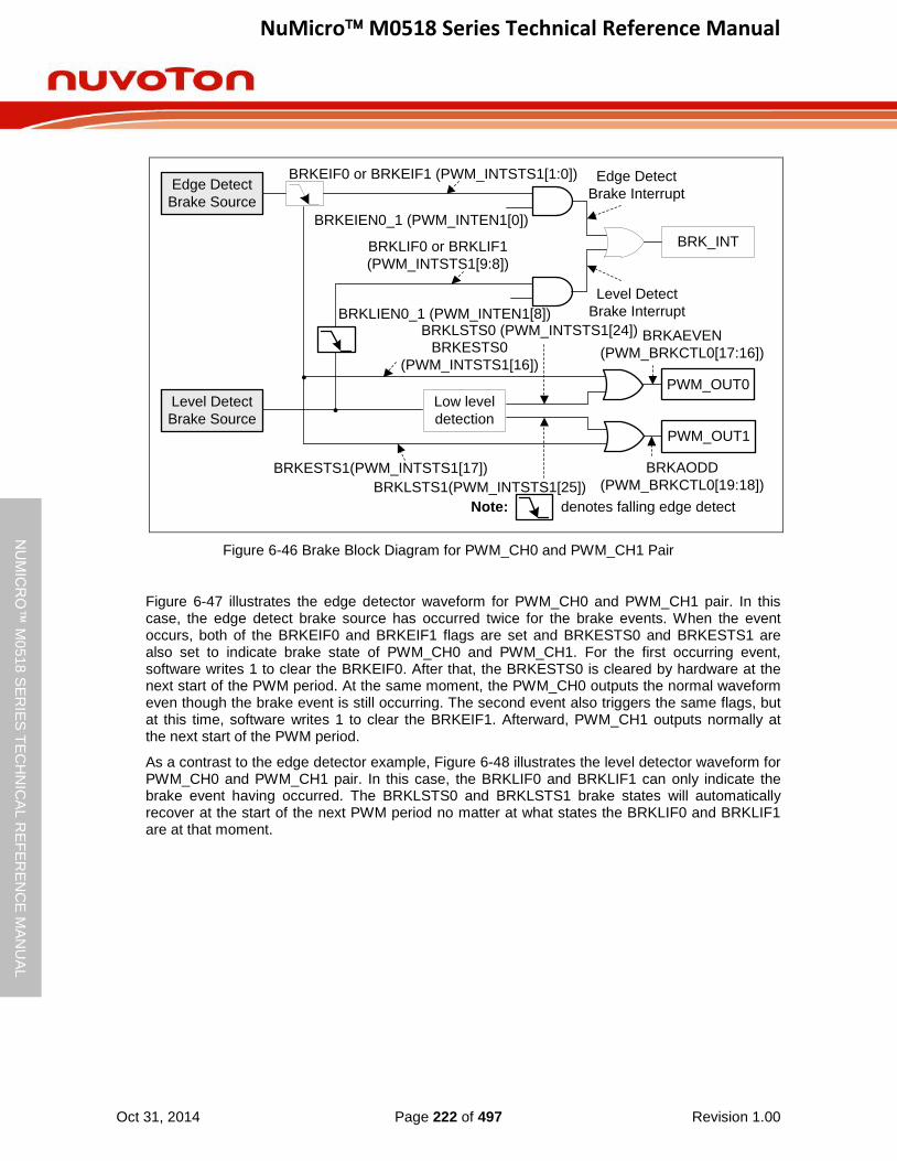
NuMicro M0518 Series Technical Reference Manual
Oct 31, 2014 Page 222 of 497 Revision 1.00
NU
MIC
RO
™ M
0518
SE
RIE
S T
EC
HN
ICA
L R
EF
ER
EN
CE
MA
NU
AL
Edge Detect
Brake Interrupt
BRKEIF0 or BRKEIF1 (PWM_INTSTS1[1:0])
BRK_INT
Low level
detection
Level Detect
Brake Interrupt
BRKEIEN0_1 (PWM_INTEN1[0])
BRKLIF0 or BRKLIF1
(PWM_INTSTS1[9:8])
BRKLIEN0_1 (PWM_INTEN1[8])
Edge Detect
Brake Source
Level Detect
Brake Source
Note: denotes falling edge detect
BRKESTS0
(PWM_INTSTS1[16])
PWM_OUT1
PWM_OUT0
BRKLSTS0 (PWM_INTSTS1[24])
BRKESTS1(PWM_INTSTS1[17])
BRKLSTS1(PWM_INTSTS1[25])
BRKAEVEN
(PWM_BRKCTL0[17:16])
BRKAODD
(PWM_BRKCTL0[19:18])
Figure 6-46 Brake Block Diagram for PWM_CH0 and PWM_CH1 Pair
Figure 6-47 illustrates the edge detector waveform for PWM_CH0 and PWM_CH1 pair. In this case, the edge detect brake source has occurred twice for the brake events. When the event occurs, both of the BRKEIF0 and BRKEIF1 flags are set and BRKESTS0 and BRKESTS1 are also set to indicate brake state of PWM_CH0 and PWM_CH1. For the first occurring event, software writes 1 to clear the BRKEIF0. After that, the BRKESTS0 is cleared by hardware at the next start of the PWM period. At the same moment, the PWM_CH0 outputs the normal waveform even though the brake event is still occurring. The second event also triggers the same flags, but at this time, software writes 1 to clear the BRKEIF1. Afterward, PWM_CH1 outputs normally at the next start of the PWM period.
As a contrast to the edge detector example, Figure 6-48 illustrates the level detector waveform for PWM_CH0 and PWM_CH1 pair. In this case, the BRKLIF0 and BRKLIF1 can only indicate the brake event having occurred. The BRKLSTS0 and BRKLSTS1 brake states will automatically recover at the start of the next PWM period no matter at what states the BRKLIF0 and BRKLIF1 are at that moment.
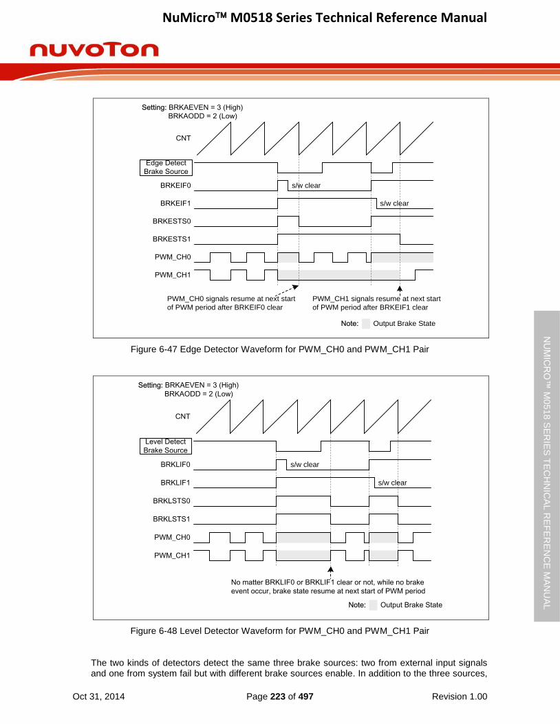
NuMicro M0518 Series Technical Reference Manual
Oct 31, 2014 Page 223 of 497 Revision 1.00
NU
MIC
RO
™ M
0518
SE
RIE
S T
EC
HN
ICA
L R
EF
ER
EN
CE
MA
NU
AL
CNT
Edge Detect
Brake Source
PWM_CH0
PWM_CH0 signals resume at next start
of PWM period after BRKEIF0 clear
BRKEIF1
BRKEIF0 s/w clear
BRKESTS0
BRKESTS1
s/w clear
PWM_CH1
PWM_CH1 signals resume at next start
of PWM period after BRKEIF1 clear
Note: Output Brake State
Setting: BRKAEVEN = 3 (High)
BRKAODD = 2 (Low)
Figure 6-47 Edge Detector Waveform for PWM_CH0 and PWM_CH1 Pair
CNT
Level Detect
Brake Source
PWM_CH0
BRKLIF1
BRKLIF0 s/w clear
BRKLSTS0
BRKLSTS1
s/w clear
PWM_CH1
No matter BRKLIF0 or BRKLIF1 clear or not, while no brake
event occur, brake state resume at next start of PWM period
Note: Output Brake State
Setting: BRKAEVEN = 3 (High)
BRKAODD = 2 (Low)
Figure 6-48 Level Detector Waveform for PWM_CH0 and PWM_CH1 Pair
The two kinds of detectors detect the same three brake sources: two from external input signals and one from system fail but with different brake sources enable. In addition to the three sources,
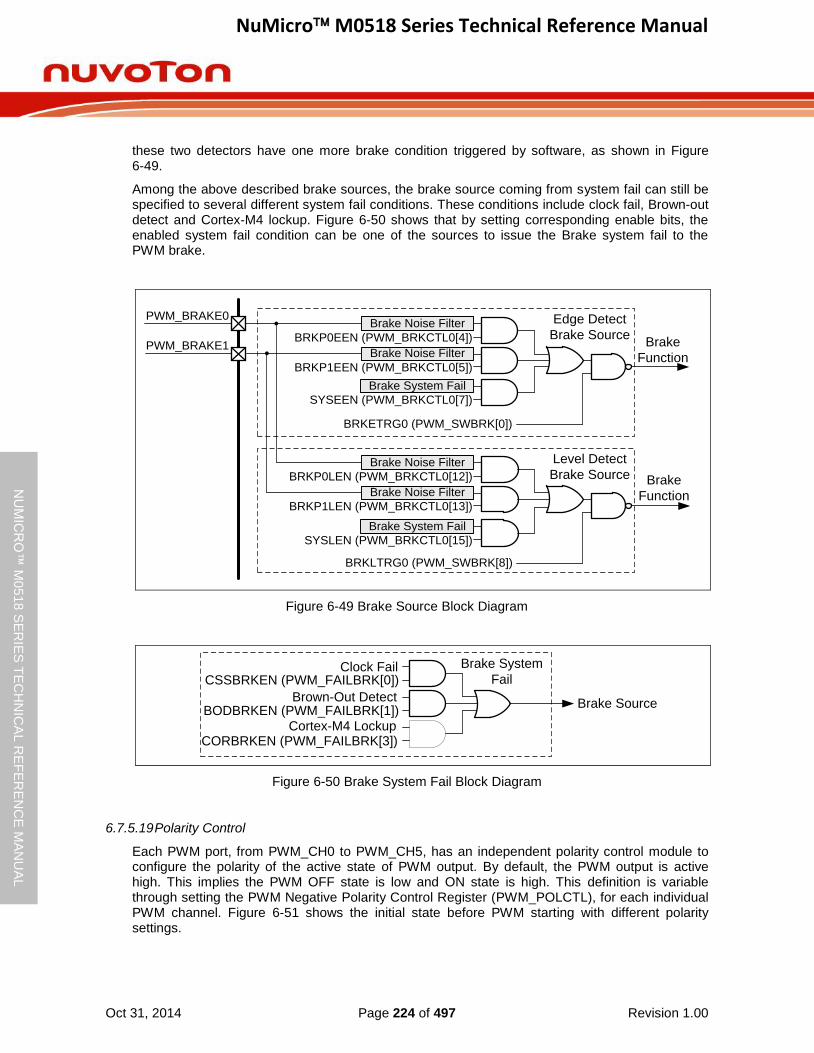
NuMicro M0518 Series Technical Reference Manual
Oct 31, 2014 Page 224 of 497 Revision 1.00
NU
MIC
RO
™ M
0518
SE
RIE
S T
EC
HN
ICA
L R
EF
ER
EN
CE
MA
NU
AL
these two detectors have one more brake condition triggered by software, as shown in Figure 6-49.
Among the above described brake sources, the brake source coming from system fail can still be specified to several different system fail conditions. These conditions include clock fail, Brown-out detect and Cortex-M4 lockup. Figure 6-50 shows that by setting corresponding enable bits, the enabled system fail condition can be one of the sources to issue the Brake system fail to the PWM brake.
BRKLTRG0 (PWM_SWBRK[8])
Brake System Fail
BRKP0LEN (PWM_BRKCTL0[12])
BRKP1LEN (PWM_BRKCTL0[13])
SYSLEN (PWM_BRKCTL0[15])
Brake System Fail
BRKP0EEN (PWM_BRKCTL0[4])
Brake Noise Filter
BRKP1EEN (PWM_BRKCTL0[5])
SYSEEN (PWM_BRKCTL0[7])
PWM_BRAKE0
Brake Noise FilterPWM_BRAKE1
Brake Noise Filter
Brake Noise Filter
Brake
Function
Brake
Function
Edge Detect
Brake Source
Level Detect
Brake Source
BRKETRG0 (PWM_SWBRK[0])
Figure 6-49 Brake Source Block Diagram
CSSBRKEN (PWM_FAILBRK[0])Clock Fail
BODBRKEN (PWM_FAILBRK[1])Brown-Out Detect
CORBRKEN (PWM_FAILBRK[3])Cortex-M4 Lockup
Brake Source
Brake System
Fail
Figure 6-50 Brake System Fail Block Diagram
6.7.5.19 Polarity Control
Each PWM port, from PWM_CH0 to PWM_CH5, has an independent polarity control module to configure the polarity of the active state of PWM output. By default, the PWM output is active high. This implies the PWM OFF state is low and ON state is high. This definition is variable through setting the PWM Negative Polarity Control Register (PWM_POLCTL), for each individual PWM channel. Figure 6-51 shows the initial state before PWM starting with different polarity settings.
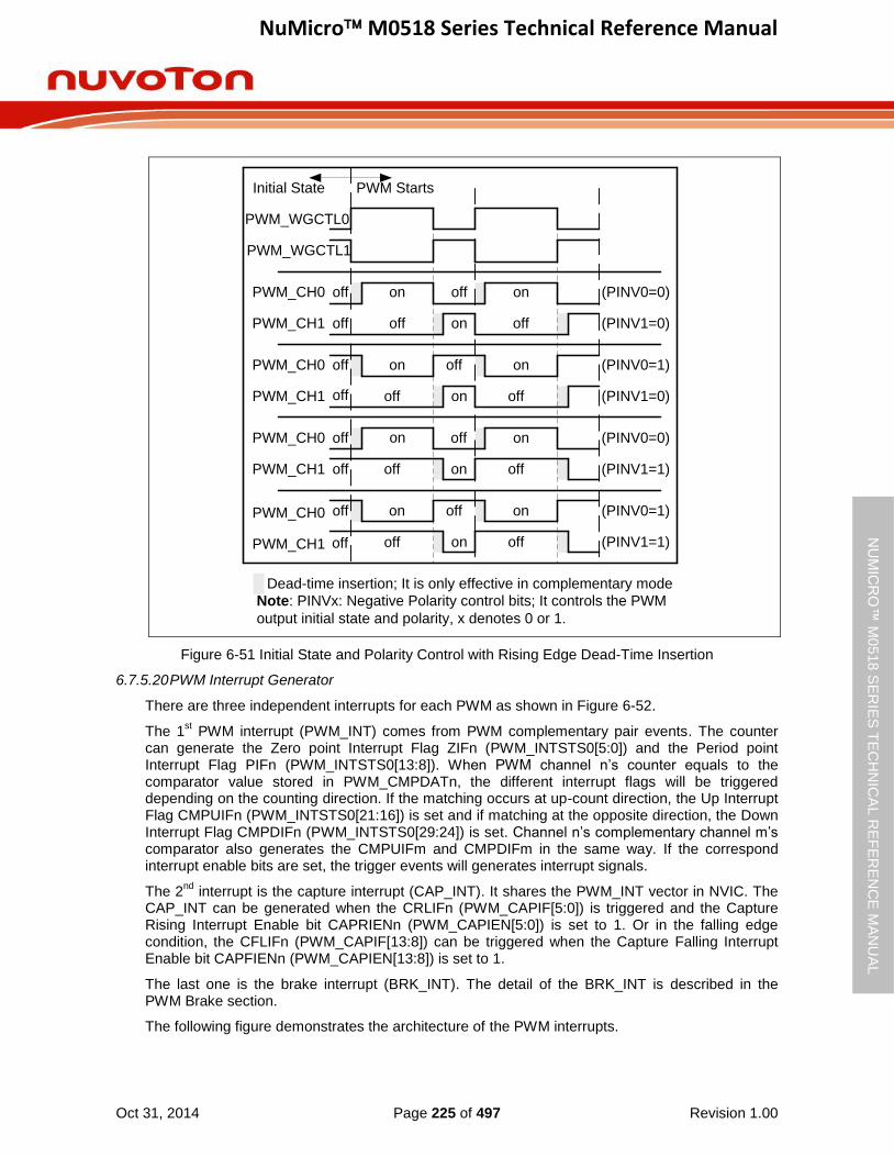
NuMicro M0518 Series Technical Reference Manual
Oct 31, 2014 Page 225 of 497 Revision 1.00
NU
MIC
RO
™ M
0518
SE
RIE
S T
EC
HN
ICA
L R
EF
ER
EN
CE
MA
NU
AL
PWM_WGCTL0
PWM_WGCTL1
PWM_CH0
PWM_CH1
off on on
off
off
off on off
(PINV0=0)
(PINV1=0)
Dead-time insertion; It is only effective in complementary modeNote: PINVx: Negative Polarity control bits; It controls the PWM
output initial state and polarity, x denotes 0 or 1.
PWM_CH0
PWM_CH1
PWM_CH0
PWM_CH1
PWM_CH0
PWM_CH1
(PINV0=1)
(PINV1=0)
(PINV0=0)
(PINV1=1)
(PINV0=1)
(PINV1=1)
Initial State PWM Starts
onoff off on
off off on off
off on onoff
off off on off
off off on off
onoff off on
Figure 6-51 Initial State and Polarity Control with Rising Edge Dead-Time Insertion
6.7.5.20 PWM Interrupt Generator
There are three independent interrupts for each PWM as shown in Figure 6-52.
The 1st PWM interrupt (PWM_INT) comes from PWM complementary pair events. The counter
can generate the Zero point Interrupt Flag ZIFn (PWM_INTSTS0[5:0]) and the Period point Interrupt Flag PIFn (PWM_INTSTS0[13:8]). When PWM channel n’s counter equals to the comparator value stored in PWM_CMPDATn, the different interrupt flags will be triggered depending on the counting direction. If the matching occurs at up-count direction, the Up Interrupt Flag CMPUIFn (PWM_INTSTS0[21:16]) is set and if matching at the opposite direction, the Down Interrupt Flag CMPDIFn (PWM_INTSTS0[29:24]) is set. Channel n’s complementary channel m’s comparator also generates the CMPUIFm and CMPDIFm in the same way. If the correspond interrupt enable bits are set, the trigger events will generates interrupt signals.
The 2nd
interrupt is the capture interrupt (CAP_INT). It shares the PWM_INT vector in NVIC. The CAP_INT can be generated when the CRLIFn (PWM_CAPIF[5:0]) is triggered and the Capture Rising Interrupt Enable bit CAPRIENn (PWM_CAPIEN[5:0]) is set to 1. Or in the falling edge condition, the CFLIFn (PWM_CAPIF[13:8]) can be triggered when the Capture Falling Interrupt Enable bit CAPFIENn (PWM_CAPIEN[13:8]) is set to 1.
The last one is the brake interrupt (BRK_INT). The detail of the BRK_INT is described in the PWM Brake section.
The following figure demonstrates the architecture of the PWM interrupts.
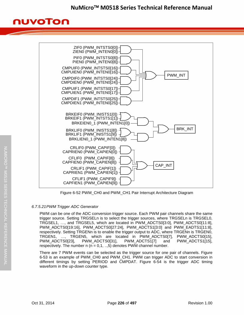
NuMicro M0518 Series Technical Reference Manual
Oct 31, 2014 Page 226 of 497 Revision 1.00
NU
MIC
RO
™ M
0518
SE
RIE
S T
EC
HN
ICA
L R
EF
ER
EN
CE
MA
NU
AL
BRKEIF0 (PWM_INISTS1[0])BRKEIF1 (PWM_INTSTS1[1])
BRK_INT
BRKEIEN0_1 (PWM_INTEN1[0])
CRLIF0 (PWM_CAPIF[0])
PWM_INT
CAP_INT
ZIEN0 (PWM_INTEN0[0])ZIF0 (PWM_INTSTS0[0])
PIEN0 (PWM_INTEN0[8])PIF0 (PWM_INTSTS0[8])
CMPUIEN0 (PWM_INTEN0[16])CMPUIF0 (PWM_INTSTS0[16])
CMPDIEN0 (PWM_INTEN0[24])CMPDIF0 (PWM_INTSTS0[24])
CMPUIEN1 (PWM_INTEN0[17])CMPUIF1 (PWM_INTSTS0[17])
CMPDIEN1 (PWM_INTEN0[25])CMPDIF1 (PWM_INTSTS0[25])
CAPRIEN0 (PWM_CAPIEN[0])
CFLIF0 (PWM_CAPIF[8])CAPFIEN0 (PWM_CAPIEN[8])
CRLIF1 (PWM_CAPIF[1])CAPRIEN1 (PWM_CAPIEN[1])
CFLIF1 (PWM_CAPIF9])CAPFIEN1 (PWM_CAPIEN[9])
BRKLIF0 (PWM_INISTS1[8])BRKLIF1 (PWM_INISTS1[9])
BRKLIEN0_1 (PWM_INTEN1[8])
Figure 6-52 PWM_CH0 and PWM_CH1 Pair Interrupt Architecture Diagram
6.7.5.21 PWM Trigger ADC Generator
PWM can be one of the ADC conversion trigger source. Each PWM pair channels share the same trigger source. Setting TRGSELn is to select the trigger sources, where TRGSELn is TRGSEL0, TRGSEL1, …, and TRGSEL5, which are located in PWM_ADCTS0[3:0], PWM_ADCTS0[11:8], PWM_ADCTS0[19:16], PWM_ADCTS0[27:24], PWM_ADCTS1[3:0] and PWM_EADTS1[11:8], respectively. Setting TRGENn is to enable the trigger output to ADC, where TRGENn is TRGEN0, TRGEN1, …, TRGEN5, which are located in PWM_ADCTS0[7], PWM_ADCTS0[15], PWM_ADCTS0[23], PWM_ADCTS0[31], PWM_ADCTS1[7] and PWM_ADCTS1[15], respectively. The number n (n = 0,1, ..,5) denotes PWM channel number.
There are 7 PWM events can be selected as the trigger source for one pair of channels. Figure 6-53 is an example of PWM_CH0 and PWM_CH1. PWM can trigger ADC to start conversion in different timings by setting PERIOD and CMPDAT. Figure 6-54 is the trigger ADC timing waveform in the up-down counter type.
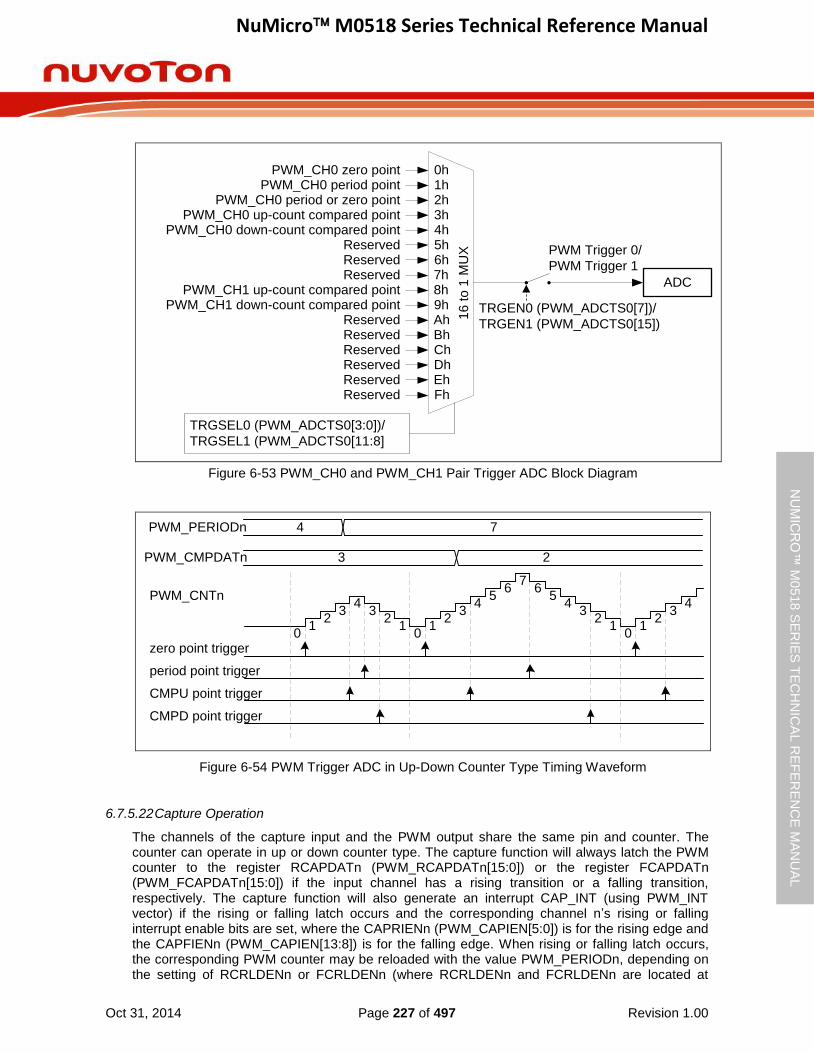
NuMicro M0518 Series Technical Reference Manual
Oct 31, 2014 Page 227 of 497 Revision 1.00
NU
MIC
RO
™ M
0518
SE
RIE
S T
EC
HN
ICA
L R
EF
ER
EN
CE
MA
NU
AL
16
to
1 M
UX
2h3h
0h1h
6h7h
4h5h
Fh
PWM_CH1 down-count compared point
PWM_CH0 zero pointPWM_CH0 period point
PWM_CH0 up-count compared pointPWM_CH0 down-count compared point
PWM_CH1 up-count compared point
PWM Trigger 0/
PWM Trigger 1
Reserved9hAh
8h
DhEh
BhCh
TRGSEL0 (PWM_ADCTS0[3:0])/
TRGSEL1 (PWM_ADCTS0[11:8]
TRGEN0 (PWM_ADCTS0[7])/
TRGEN1 (PWM_ADCTS0[15])
PWM_CH0 period or zero point
ADC
ReservedReservedReservedReservedReserved
ReservedReservedReserved
Figure 6-53 PWM_CH0 and PWM_CH1 Pair Trigger ADC Block Diagram
PWM_CMPDATn
PWM_PERIODn
zero point trigger
PWM_CNTn
4 7
3 2
01
23
43
12
01
23
43
12
0
56
76
45
12
34
period point trigger
CMPU point trigger
CMPD point trigger
Figure 6-54 PWM Trigger ADC in Up-Down Counter Type Timing Waveform
6.7.5.22 Capture Operation
The channels of the capture input and the PWM output share the same pin and counter. The counter can operate in up or down counter type. The capture function will always latch the PWM counter to the register RCAPDATn (PWM_RCAPDATn[15:0]) or the register FCAPDATn (PWM_FCAPDATn[15:0]) if the input channel has a rising transition or a falling transition, respectively. The capture function will also generate an interrupt CAP_INT (using PWM_INT vector) if the rising or falling latch occurs and the corresponding channel n’s rising or falling interrupt enable bits are set, where the CAPRIENn (PWM_CAPIEN[5:0]) is for the rising edge and the CAPFIENn (PWM_CAPIEN[13:8]) is for the falling edge. When rising or falling latch occurs, the corresponding PWM counter may be reloaded with the value PWM_PERIODn, depending on the setting of RCRLDENn or FCRLDENn (where RCRLDENn and FCRLDENn are located at
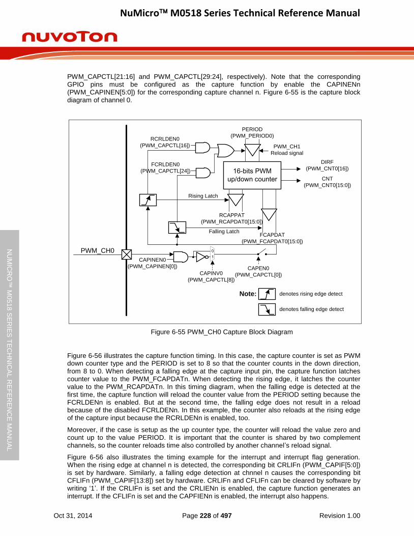
NuMicro M0518 Series Technical Reference Manual
Oct 31, 2014 Page 228 of 497 Revision 1.00
NU
MIC
RO
™ M
0518
SE
RIE
S T
EC
HN
ICA
L R
EF
ER
EN
CE
MA
NU
AL
PWM_CAPCTL[21:16] and PWM_CAPCTL[29:24], respectively). Note that the corresponding GPIO pins must be configured as the capture function by enable the CAPINENn (PWM_CAPINEN[5:0]) for the corresponding capture channel n. Figure 6-55 is the capture block diagram of channel 0.
0
1
16-bits PWM
up/down counter CNT
(PWM_CNT0[15:0])
DIRF
(PWM_CNT0[16])
PERIOD
(PWM_PERIOD0)
RCAPPAT
(PWM_RCAPDAT0[15:0])
FCAPDAT
(PWM_FCAPDAT0[15:0])
CAPEN0
(PWM_CAPCTL[0])CAPINV0
(PWM_CAPCTL[8])
CAPINEN0
(PWM_CAPINEN[0])
PWM_CH0
RCRLDEN0
(PWM_CAPCTL[16])
FCRLDEN0
(PWM_CAPCTL[24])
Note: denotes rising edge detect
denotes falling edge detect
Rising Latch
Falling Latch
PWM_CH1
Reload signal
Figure 6-55 PWM_CH0 Capture Block Diagram
Figure 6-56 illustrates the capture function timing. In this case, the capture counter is set as PWM down counter type and the PERIOD is set to 8 so that the counter counts in the down direction, from 8 to 0. When detecting a falling edge at the capture input pin, the capture function latches counter value to the PWM_FCAPDATn. When detecting the rising edge, it latches the counter value to the PWM_RCAPDATn. In this timing diagram, when the falling edge is detected at the first time, the capture function will reload the counter value from the PERIOD setting because the FCRLDENn is enabled. But at the second time, the falling edge does not result in a reload because of the disabled FCRLDENn. In this example, the counter also reloads at the rising edge of the capture input because the RCRLDENn is enabled, too.
Moreover, if the case is setup as the up counter type, the counter will reload the value zero and count up to the value PERIOD. It is important that the counter is shared by two complement channels, so the counter reloads time also controlled by another channel’s reload signal.
Figure 6-56 also illustrates the timing example for the interrupt and interrupt flag generation. When the rising edge at channel n is detected, the corresponding bit CRLIFn (PWM_CAPIF[5:0]) is set by hardware. Similarly, a falling edge detection at chnnel n causes the corresponding bit CFLIFn (PWM_CAPIF[13:8]) set by hardware. CRLIFn and CFLIFn can be cleared by software by writing ‘1’. If the CRLIFn is set and the CRLIENn is enabled, the capture function generates an interrupt. If the CFLIFn is set and the CAPFIENn is enabled, the interrupt also happens.

NuMicro M0518 Series Technical Reference Manual
Oct 31, 2014 Page 229 of 497 Revision 1.00
NU
MIC
RO
™ M
0518
SE
RIE
S T
EC
HN
ICA
L R
EF
ER
EN
CE
MA
NU
AL
A condition which is not shown in this figure is: if the rising latch happens again when the CRLIF is already set, the Over run status CRLIFOVn (PWM_CAPSTS[5:0]) will be set to 1 by hardware to indicate the CRLIF overrunning. Also, if the falling latch happens again, the same hardware operation occurs for the interrupt flag CFLIF and the Over run status CFLIFOVn (PWM_CAPSTS[13:8]).
Note: n denotes 0 to 5
8 7 6 5 43 2 1 8 7 6 5PWM counter
1 7
Capture Input
PWM_FCAPDATn
5PWM_RCAPDATn
Capture interrupt
CAPFIENn
CAPRIENn
CAPINENn
Clear by S/WCFLIFn
CRLIFn
Reload (PERIOD = 8) Reload
Clear by S/W
Falling Latch Falling Latch
Rising Latch
FCRLDENn
RCRLDENn
Figure 6-56 Capture Operation Waveform
The capture pulse width can be calculated according to the following formula:
For the negative pulse case, the channel low pulse width is calculated as (PWM_PERIODn + 1 - PWM_RCAPDATn). In Figure 6-56 case, the low pulse width is 8+1-5 = 4
For the positive pulse case, the channel high pulse width is calculated as (PWM_PERIODn + 1 -
PWM_FCAPDATn). In Figure 6-56 case, high pulse width is 8+1-7 = 2

NuMicro M0518 Series Technical Reference Manual
Oct 31, 2014 Page 230 of 497 Revision 1.00
NU
MIC
RO
™ M
0518
SE
RIE
S T
EC
HN
ICA
L R
EF
ER
EN
CE
MA
NU
AL
6.7.6 Register Map
R: read only, W: write only, R/W: both read and write
Register Offset R/W Description Reset Value
PWM Base Address:
PWM0_BA = 0x4004_0000
PWM1_BA = 0x4014_0000
PWM_CTL0
x=0, 1 PWMx_BA+0x00 R/W PWM Control Register 0 0x0000_0000
PWM_CTL1
x=0, 1 PWMx_BA+0x04 R/W PWM Control Register 1 0x0000_0000
PWM_CLKSRC
x=0, 1 PWMx_BA+0x10 R/W PWM Clock Source Register 0x0000_0000
PWM_CLKPSC0_1
x=0, 1
PWMx_BA+0x14 R/W PWM Clock Pre-scale Register 0 0x0000_0000
PWM_CLKPSC2_3
x=0, 1
PWMx_BA+0x18 R/W PWM Clock Pre-scale Register 2 0x0000_0000
PWM_CLKPSC4_5
x=0, 1
PWMx_BA+0x1C R/W PWM Clock Pre-scale Register 4 0x0000_0000
PWM_CNTEN
x=0, 1 PWMx_BA+0x20 R/W PWM Counter Enable Register 0x0000_0000
PWM_CNTCLR
x=0, 1 PWMx_BA+0x24 R/W PWM Clear Counter Register 0x0000_0000
PWM_PERIOD0
x=0, 1 PWMx_BA+0x30 R/W PWM Period Register 0 0x0000_0000
PWM_PERIOD2
x=0, 1 PWMx_BA+0x38 R/W PWM Period Register 2 0x0000_0000
PWM_PERIOD4
x=0, 1 PWMx_BA+0x40 R/W PWM Period Register 4 0x0000_0000
PWM_CMPDAT0
x=0, 1 PWMx_BA+0x50 R/W PWM Comparator Register 0 0x0000_0000
PWM_CMPDAT1
x=0, 1 PWMx_BA+0x54 R/W PWM Comparator Register 1 0x0000_0000
PWM_CMPDAT2
x=0, 1 PWMx_BA+0x58 R/W PWM Comparator Register 2 0x0000_0000
PWM_CMPDAT3
x=0, 1 PWMx_BA+0x5C R/W PWM Comparator Register 3 0x0000_0000
PWM_CMPDAT4 PWMx_BA+0x60 R/W PWM Comparator Register 4 0x0000_0000
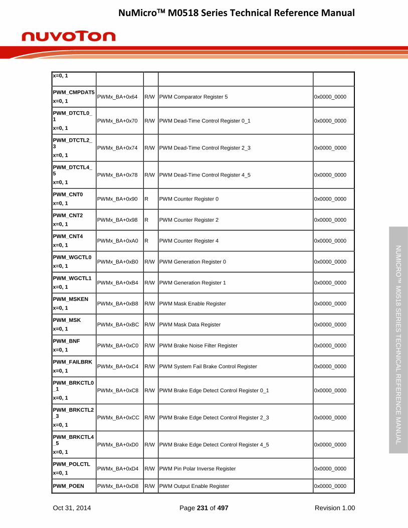
NuMicro M0518 Series Technical Reference Manual
Oct 31, 2014 Page 231 of 497 Revision 1.00
NU
MIC
RO
™ M
0518
SE
RIE
S T
EC
HN
ICA
L R
EF
ER
EN
CE
MA
NU
AL
x=0, 1
PWM_CMPDAT5
x=0, 1 PWMx_BA+0x64 R/W PWM Comparator Register 5 0x0000_0000
PWM_DTCTL0_1
x=0, 1
PWMx_BA+0x70 R/W PWM Dead-Time Control Register 0_1 0x0000_0000
PWM_DTCTL2_3
x=0, 1
PWMx_BA+0x74 R/W PWM Dead-Time Control Register 2_3 0x0000_0000
PWM_DTCTL4_5
x=0, 1
PWMx_BA+0x78 R/W PWM Dead-Time Control Register 4_5 0x0000_0000
PWM_CNT0
x=0, 1 PWMx_BA+0x90 R PWM Counter Register 0 0x0000_0000
PWM_CNT2
x=0, 1 PWMx_BA+0x98 R PWM Counter Register 2 0x0000_0000
PWM_CNT4
x=0, 1 PWMx_BA+0xA0 R PWM Counter Register 4 0x0000_0000
PWM_WGCTL0
x=0, 1 PWMx_BA+0xB0 R/W PWM Generation Register 0 0x0000_0000
PWM_WGCTL1
x=0, 1 PWMx_BA+0xB4 R/W PWM Generation Register 1 0x0000_0000
PWM_MSKEN
x=0, 1 PWMx_BA+0xB8 R/W PWM Mask Enable Register 0x0000_0000
PWM_MSK
x=0, 1 PWMx_BA+0xBC R/W PWM Mask Data Register 0x0000_0000
PWM_BNF
x=0, 1 PWMx_BA+0xC0 R/W PWM Brake Noise Filter Register 0x0000_0000
PWM_FAILBRK
x=0, 1 PWMx_BA+0xC4 R/W PWM System Fail Brake Control Register 0x0000_0000
PWM_BRKCTL0_1
x=0, 1
PWMx_BA+0xC8 R/W PWM Brake Edge Detect Control Register 0_1 0x0000_0000
PWM_BRKCTL2_3
x=0, 1
PWMx_BA+0xCC R/W PWM Brake Edge Detect Control Register 2_3 0x0000_0000
PWM_BRKCTL4_5
x=0, 1
PWMx_BA+0xD0 R/W PWM Brake Edge Detect Control Register 4_5 0x0000_0000
PWM_POLCTL
x=0, 1 PWMx_BA+0xD4 R/W PWM Pin Polar Inverse Register 0x0000_0000
PWM_POEN PWMx_BA+0xD8 R/W PWM Output Enable Register 0x0000_0000
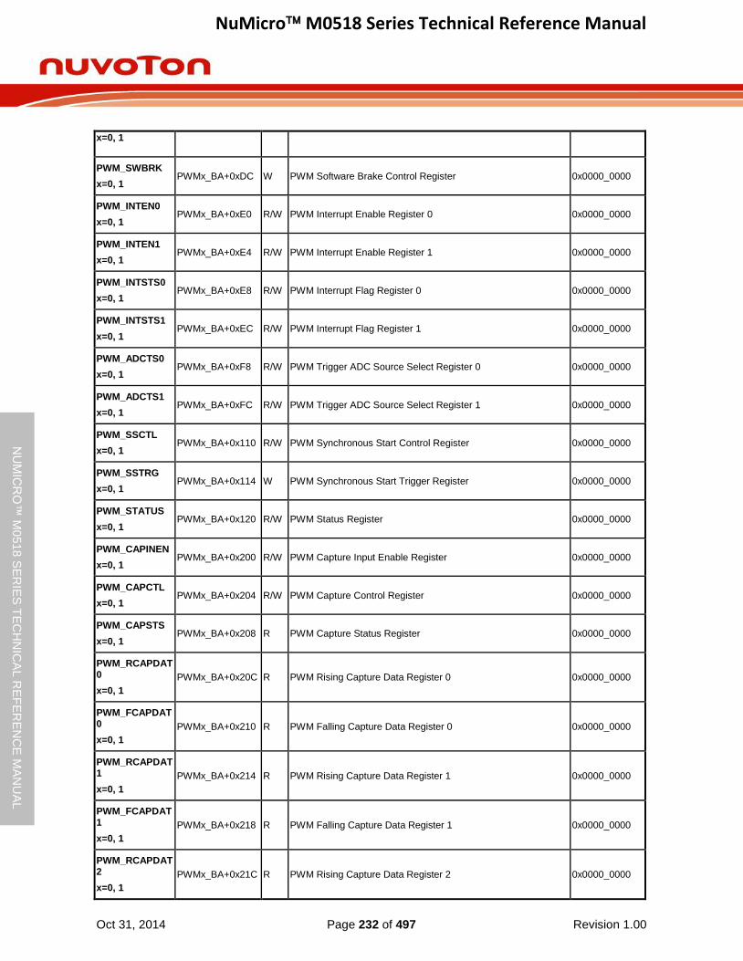
NuMicro M0518 Series Technical Reference Manual
Oct 31, 2014 Page 232 of 497 Revision 1.00
NU
MIC
RO
™ M
0518
SE
RIE
S T
EC
HN
ICA
L R
EF
ER
EN
CE
MA
NU
AL
x=0, 1
PWM_SWBRK
x=0, 1 PWMx_BA+0xDC W PWM Software Brake Control Register 0x0000_0000
PWM_INTEN0
x=0, 1 PWMx_BA+0xE0 R/W PWM Interrupt Enable Register 0 0x0000_0000
PWM_INTEN1
x=0, 1 PWMx_BA+0xE4 R/W PWM Interrupt Enable Register 1 0x0000_0000
PWM_INTSTS0
x=0, 1 PWMx_BA+0xE8 R/W PWM Interrupt Flag Register 0 0x0000_0000
PWM_INTSTS1
x=0, 1 PWMx_BA+0xEC R/W PWM Interrupt Flag Register 1 0x0000_0000
PWM_ADCTS0
x=0, 1 PWMx_BA+0xF8 R/W PWM Trigger ADC Source Select Register 0 0x0000_0000
PWM_ADCTS1
x=0, 1 PWMx_BA+0xFC R/W PWM Trigger ADC Source Select Register 1 0x0000_0000
PWM_SSCTL
x=0, 1 PWMx_BA+0x110 R/W PWM Synchronous Start Control Register 0x0000_0000
PWM_SSTRG
x=0, 1 PWMx_BA+0x114 W PWM Synchronous Start Trigger Register 0x0000_0000
PWM_STATUS
x=0, 1 PWMx_BA+0x120 R/W PWM Status Register 0x0000_0000
PWM_CAPINEN
x=0, 1 PWMx_BA+0x200 R/W PWM Capture Input Enable Register 0x0000_0000
PWM_CAPCTL
x=0, 1 PWMx_BA+0x204 R/W PWM Capture Control Register 0x0000_0000
PWM_CAPSTS
x=0, 1 PWMx_BA+0x208 R PWM Capture Status Register 0x0000_0000
PWM_RCAPDAT0
x=0, 1
PWMx_BA+0x20C R PWM Rising Capture Data Register 0 0x0000_0000
PWM_FCAPDAT0
x=0, 1
PWMx_BA+0x210 R PWM Falling Capture Data Register 0 0x0000_0000
PWM_RCAPDAT1
x=0, 1
PWMx_BA+0x214 R PWM Rising Capture Data Register 1 0x0000_0000
PWM_FCAPDAT1
x=0, 1
PWMx_BA+0x218 R PWM Falling Capture Data Register 1 0x0000_0000
PWM_RCAPDAT2
x=0, 1
PWMx_BA+0x21C R PWM Rising Capture Data Register 2 0x0000_0000

NuMicro M0518 Series Technical Reference Manual
Oct 31, 2014 Page 233 of 497 Revision 1.00
NU
MIC
RO
™ M
0518
SE
RIE
S T
EC
HN
ICA
L R
EF
ER
EN
CE
MA
NU
AL
PWM_FCAPDAT2
x=0, 1
PWMx_BA+0x220 R PWM Falling Capture Data Register 2 0x0000_0000
PWM_RCAPDAT3
x=0, 1
PWMx_BA+0x224 R PWM Rising Capture Data Register 3 0x0000_0000
PWM_FCAPDAT3
x=0, 1
PWMx_BA+0x228 R PWM Falling Capture Data Register 3 0x0000_0000
PWM_RCAPDAT4
x=0, 1
PWMx_BA+0x22C R PWM Rising Capture Data Register 4 0x0000_0000
PWM_FCAPDAT4
x=0, 1
PWMx_BA+0x230 R PWM Falling Capture Data Register 4 0x0000_0000
PWM_RCAPDAT5
x=0, 1
PWMx_BA+0x234 R PWM Rising Capture Data Register 5 0x0000_0000
PWM_FCAPDAT5
x=0, 1
PWMx_BA+0x238 R PWM Falling Capture Data Register 5 0x0000_0000
PWM_CAPIEN
x=0, 1 PWMx_BA+0x250 R/W PWM Capture Interrupt Enable Register 0x0000_0000
PWM_CAPIF
x=0, 1 PWMx_BA+0x254 R/W PWM Capture Interrupt Flag Register 0x0000_0000
PWM_PBUF0
x=0, 1 PWMx_BA+0x304 R PWM PERIOD0 Buffer 0x0000_0000
PWM_PBUF2
x=0, 1 PWMx_BA+0x30C R PWM PERIOD2 Buffer 0x0000_0000
PWM_PBUF4
x=0, 1 PWMx_BA+0x314 R PWM PERIOD4 Buffer 0x0000_0000
PWM_CMPBUF0
x=0, 1 PWMx_BA+0x31C R PWM CMPDAT0 Buffer 0x0000_0000
PWM_CMPBUF1
x=0, 1 PWMx_BA+0x320 R PWM CMPDAT1 Buffer 0x0000_0000
PWM_CMPBUF2
x=0, 1 PWMx_BA+0x324 R PWM CMPDAT2 Buffer 0x0000_0000
PWM_CMPBUF3
x=0, 1 PWMx_BA+0x328 R PWM CMPDAT3 Buffer 0x0000_0000
PWM_CMPBUF4
x=0, 1 PWMx_BA+0x32C R PWM CMPDAT4 Buffer 0x0000_0000
PWM_CMPBUF5
x=0, 1 PWMx_BA+0x330 R PWM CMPDAT5 Buffer 0x0000_0000
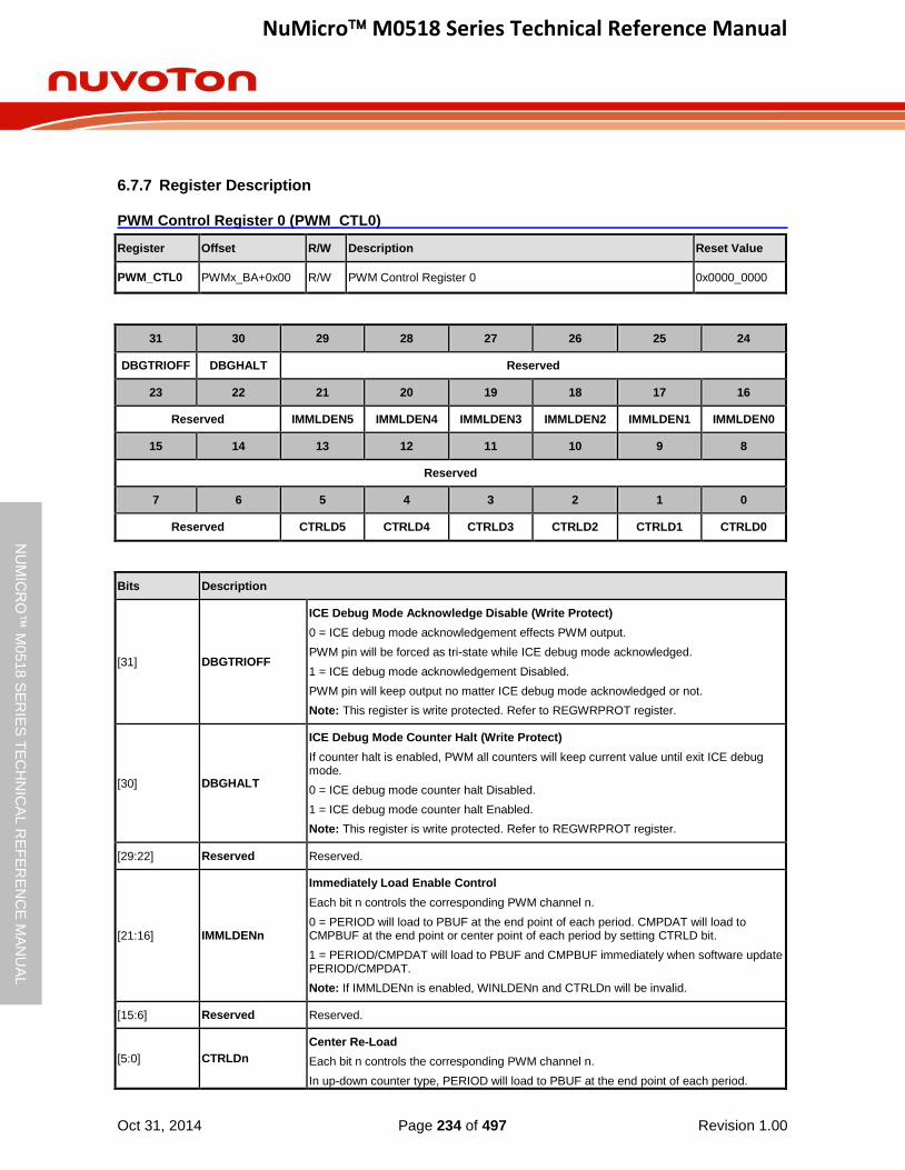
NuMicro M0518 Series Technical Reference Manual
Oct 31, 2014 Page 234 of 497 Revision 1.00
NU
MIC
RO
™ M
0518
SE
RIE
S T
EC
HN
ICA
L R
EF
ER
EN
CE
MA
NU
AL
6.7.7 Register Description
PWM Control Register 0 (PWM_CTL0)
Register Offset R/W Description Reset Value
PWM_CTL0 PWMx_BA+0x00 R/W PWM Control Register 0 0x0000_0000
31 30 29 28 27 26 25 24
DBGTRIOFF DBGHALT Reserved
23 22 21 20 19 18 17 16
Reserved IMMLDEN5 IMMLDEN4 IMMLDEN3 IMMLDEN2 IMMLDEN1 IMMLDEN0
15 14 13 12 11 10 9 8
Reserved
7 6 5 4 3 2 1 0
Reserved CTRLD5 CTRLD4 CTRLD3 CTRLD2 CTRLD1 CTRLD0
Bits Description
[31] DBGTRIOFF
ICE Debug Mode Acknowledge Disable (Write Protect)
0 = ICE debug mode acknowledgement effects PWM output.
PWM pin will be forced as tri-state while ICE debug mode acknowledged.
1 = ICE debug mode acknowledgement Disabled.
PWM pin will keep output no matter ICE debug mode acknowledged or not.
Note: This register is write protected. Refer to REGWRPROT register.
[30] DBGHALT
ICE Debug Mode Counter Halt (Write Protect)
If counter halt is enabled, PWM all counters will keep current value until exit ICE debug mode.
0 = ICE debug mode counter halt Disabled.
1 = ICE debug mode counter halt Enabled.
Note: This register is write protected. Refer to REGWRPROT register.
[29:22] Reserved Reserved.
[21:16] IMMLDENn
Immediately Load Enable Control
Each bit n controls the corresponding PWM channel n.
0 = PERIOD will load to PBUF at the end point of each period. CMPDAT will load to CMPBUF at the end point or center point of each period by setting CTRLD bit.
1 = PERIOD/CMPDAT will load to PBUF and CMPBUF immediately when software update PERIOD/CMPDAT.
Note: If IMMLDENn is enabled, WINLDENn and CTRLDn will be invalid.
[15:6] Reserved Reserved.
[5:0] CTRLDn
Center Re-Load
Each bit n controls the corresponding PWM channel n.
In up-down counter type, PERIOD will load to PBUF at the end point of each period.

NuMicro M0518 Series Technical Reference Manual
Oct 31, 2014 Page 235 of 497 Revision 1.00
NU
MIC
RO
™ M
0518
SE
RIE
S T
EC
HN
ICA
L R
EF
ER
EN
CE
MA
NU
AL
CMPDAT will load to CMPBUF at the center point of a period.

NuMicro M0518 Series Technical Reference Manual
Oct 31, 2014 Page 236 of 497 Revision 1.00
NU
MIC
RO
™ M
0518
SE
RIE
S T
EC
HN
ICA
L R
EF
ER
EN
CE
MA
NU
AL
PWM Control Register 1 (PWM_CTL1)
Register Offset R/W Description Reset Value
PWM_CTL1 PWMx_BA+0x04 R/W PWM Control Register 1 0x0000_0000
31 30 29 28 27 26 25 24
Reserved PWMMODE4 PWMMODE2 PWMMODE0
23 22 21 20 19 18 17 16
Reserved
15 14 13 12 11 10 9 8
Reserved CNTTYPE4
7 6 5 4 3 2 1 0
Reserved CNTTYPE2 Reserved CNTTYPE0
Bits Description
[31:27] Reserved Reserved.
[26:24] PWMMODEn
PWM Mode
Each bit n controls the corresponding PWM channel n.
0 = PWM independent mode.
1 = PWM complementary mode.
Note: When operating in group function, these bits must all set to the same mode.
[23:10] Reserved Reserved.
[9:8] CNTTYPE4
PWM Counter Behavior Type 4
Each bit n controls corresponding PWM channel n.
00 = Up counter type (supports in capture mode).
01 = Down count type (supports in capture mode).
10 = Up-down counter type.
11 = Reserved.
[7:6] Reserved Reserved.
[5:4] CNTTYPE2
PWM Counter Behavior Type 2
Each bit n controls corresponding PWM channel n.
00 = Up counter type (supports in capture mode).
01 = Down count type (supports in capture mode).
10 = Up-down counter type.
11 = Reserved.
[3:2] Reserved Reserved.
[1:0] CNTTYPE0
PWM Counter Behavior Type 0
Each bit n controls corresponding PWM channel n.
00 = Up counter type (supports in capture mode).

NuMicro M0518 Series Technical Reference Manual
Oct 31, 2014 Page 237 of 497 Revision 1.00
NU
MIC
RO
™ M
0518
SE
RIE
S T
EC
HN
ICA
L R
EF
ER
EN
CE
MA
NU
AL
01 = Down count type (supports in capture mode).
10 = Up-down counter type.
11 = Reserved.
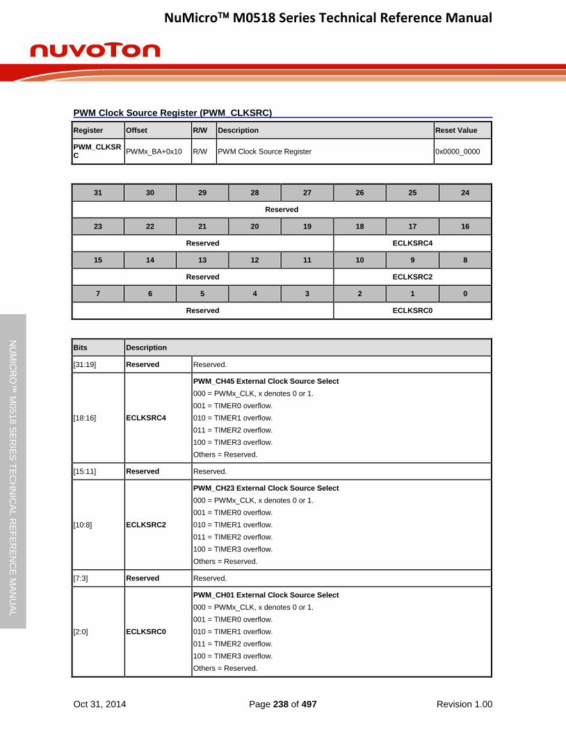
NuMicro M0518 Series Technical Reference Manual
Oct 31, 2014 Page 238 of 497 Revision 1.00
NU
MIC
RO
™ M
0518
SE
RIE
S T
EC
HN
ICA
L R
EF
ER
EN
CE
MA
NU
AL
PWM Clock Source Register (PWM_CLKSRC)
Register Offset R/W Description Reset Value
PWM_CLKSRC
PWMx_BA+0x10 R/W PWM Clock Source Register 0x0000_0000
31 30 29 28 27 26 25 24
Reserved
23 22 21 20 19 18 17 16
Reserved ECLKSRC4
15 14 13 12 11 10 9 8
Reserved ECLKSRC2
7 6 5 4 3 2 1 0
Reserved ECLKSRC0
Bits Description
[31:19] Reserved Reserved.
[18:16] ECLKSRC4
PWM_CH45 External Clock Source Select
000 = PWMx_CLK, x denotes 0 or 1.
001 = TIMER0 overflow.
010 = TIMER1 overflow.
011 = TIMER2 overflow.
100 = TIMER3 overflow.
Others = Reserved.
[15:11] Reserved Reserved.
[10:8] ECLKSRC2
PWM_CH23 External Clock Source Select
000 = PWMx_CLK, x denotes 0 or 1.
001 = TIMER0 overflow.
010 = TIMER1 overflow.
011 = TIMER2 overflow.
100 = TIMER3 overflow.
Others = Reserved.
[7:3] Reserved Reserved.
[2:0] ECLKSRC0
PWM_CH01 External Clock Source Select
000 = PWMx_CLK, x denotes 0 or 1.
001 = TIMER0 overflow.
010 = TIMER1 overflow.
011 = TIMER2 overflow.
100 = TIMER3 overflow.
Others = Reserved.
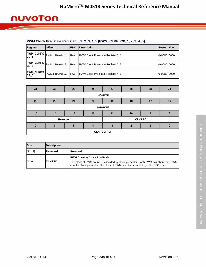
NuMicro M0518 Series Technical Reference Manual
Oct 31, 2014 Page 239 of 497 Revision 1.00
NU
MIC
RO
™ M
0518
SE
RIE
S T
EC
HN
ICA
L R
EF
ER
EN
CE
MA
NU
AL
PWM Clock Pre-Scale Register 0_1, 2_3, 4_5 (PWM_CLKPSC0_1, 2_3, 4_5)
Register Offset R/W Description Reset Value
PWM_CLKPSC0_1
PWMx_BA+0x14 R/W PWM Clock Pre-scale Register 0_1 0x0000_0000
PWM_CLKPSC2_3
PWMx_BA+0x18 R/W PWM Clock Pre-scale Register 2_3 0x0000_0000
PWM_CLKPSC4_5
PWMx_BA+0x1C R/W PWM Clock Pre-scale Register 4_5 0x0000_0000
31 30 29 28 27 26 25 24
Reserved
23 22 21 20 19 18 17 16
Reserved
15 14 13 12 11 10 9 8
Reserved CLKPSC
7 6 5 4 3 2 1 0
CLKPSC[7:0]
Bits Description
[31:12] Reserved Reserved.
[11:0] CLKPSC
PWM Counter Clock Pre-Scale
The clock of PWM counter is decided by clock prescaler. Each PWM pair share one PWM counter clock prescaler. The clock of PWM counter is divided by (CLKPSC+ 1).

NuMicro M0518 Series Technical Reference Manual
Oct 31, 2014 Page 240 of 497 Revision 1.00
NU
MIC
RO
™ M
0518
SE
RIE
S T
EC
HN
ICA
L R
EF
ER
EN
CE
MA
NU
AL
PWM Counter Enable Register (PWM_CNTEN)
Register Offset R/W Description Reset Value
PWM_CNTEN PWMx_BA+0x20 R/W PWM Counter Enable Register 0x0000_0000
31 30 29 28 27 26 25 24
Reserved
23 22 21 20 19 18 17 16
Reserved
15 14 13 12 11 10 9 8
Reserved
7 6 5 4 3 2 1 0
Reserved CNTEN4 Reserved CNTEN2 Reserved CNTEN0
Bits Description
[31:5] Reserved Reserved.
[4] CNTEN4
PWM Counter Enable 4
0 = PWM Counter and clock prescaler Stop Running.
1 = PWM Counter and clock prescaler Start Running.
[3] Reserved Reserved.
[2] CNTEN2
PWM Counter Enable 2
0 = PWM Counter and clock prescaler Stop Running.
1 = PWM Counter and clock prescaler Start Running.
[1] Reserved Reserved.
[0] CNTEN0
PWM Counter Enable 0
0 = PWM Counter and clock prescaler Stop Running.
1 = PWM Counter and clock prescaler Start Running.
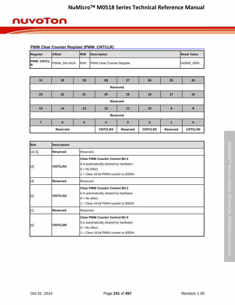
NuMicro M0518 Series Technical Reference Manual
Oct 31, 2014 Page 241 of 497 Revision 1.00
NU
MIC
RO
™ M
0518
SE
RIE
S T
EC
HN
ICA
L R
EF
ER
EN
CE
MA
NU
AL
PWM Clear Counter Register (PWM_CNTCLR)
Register Offset R/W Description Reset Value
PWM_CNTCLR
PWMx_BA+0x24 R/W PWM Clear Counter Register 0x0000_0000
31 30 29 28 27 26 25 24
Reserved
23 22 21 20 19 18 17 16
Reserved
15 14 13 12 11 10 9 8
Reserved
7 6 5 4 3 2 1 0
Reserved CNTCLR4 Reserved CNTCLR2 Reserved CNTCLR0
Bits Description
[31:5] Reserved Reserved.
[4] CNTCLR4
Clear PWM Counter Control Bit 4
It is automatically cleared by hardware.
0 = No effect.
1 = Clear 16-bit PWM counter to 0000H.
[3] Reserved Reserved.
[2] CNTCLR2
Clear PWM Counter Control Bit 2
It is automatically cleared by hardware.
0 = No effect.
1 = Clear 16-bit PWM counter to 0000H.
[1] Reserved Reserved.
[0] CNTCLR0
Clear PWM Counter Control Bit 0
It is automatically cleared by hardware.
0 = No effect.
1 = Clear 16-bit PWM counter to 0000H.

NuMicro M0518 Series Technical Reference Manual
Oct 31, 2014 Page 242 of 497 Revision 1.00
NU
MIC
RO
™ M
0518
SE
RIE
S T
EC
HN
ICA
L R
EF
ER
EN
CE
MA
NU
AL
PWM Period Register 0, 2, 4 (PWM_PERIOD0, 2, 4)
Register Offset R/W Description Reset Value
PWM_PERIOD0
PWMx_BA+0x30 R/W PWM Period Register 0 0x0000_0000
PWM_PERIOD2
PWMx_BA+0x38 R/W PWM Period Register 2 0x0000_0000
PWM_PERIOD4
PWMx_BA+0x40 R/W PWM Period Register 4 0x0000_0000
31 30 29 28 27 26 25 24
Reserved
23 22 21 20 19 18 17 16
Reserved
15 14 13 12 11 10 9 8
PERIOD
7 6 5 4 3 2 1 0
PERIOD
Bits Description
[31:16] Reserved Reserved.
[15:0] PERIOD
PWM Period Register
Up-Count mode: In this mode, PWM counter counts from 0 to PERIOD, and restarts from 0.
Down-Count mode: In this mode, PWM counter counts from PERIOD to 0, and restarts from PERIOD.
PWM period time = (PERIOD+1) * PWM_CLK period.
Up-Down-Count mode: In this mode, PWM counter counts from 0 to PERIOD, then decrements to 0 and repeats again.
PWM period time = 2 * PERIOD * PWM_CLK period.
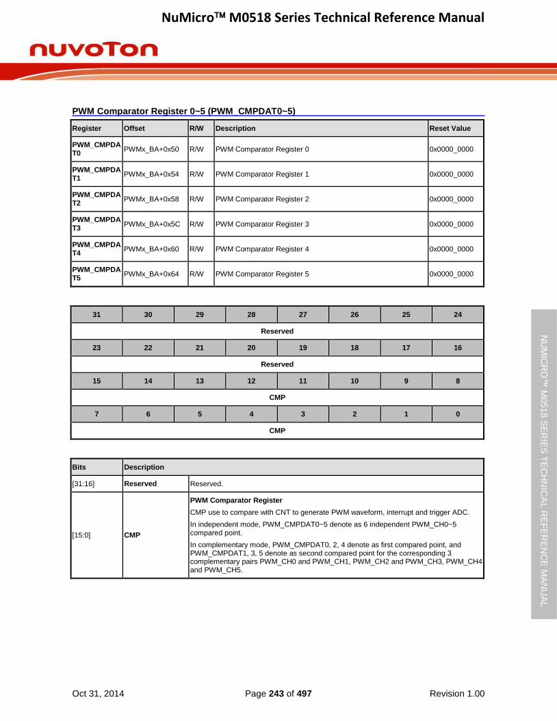
NuMicro M0518 Series Technical Reference Manual
Oct 31, 2014 Page 243 of 497 Revision 1.00
NU
MIC
RO
™ M
0518
SE
RIE
S T
EC
HN
ICA
L R
EF
ER
EN
CE
MA
NU
AL
PWM Comparator Register 0~5 (PWM_CMPDAT0~5)
Register Offset R/W Description Reset Value
PWM_CMPDAT0
PWMx_BA+0x50 R/W PWM Comparator Register 0 0x0000_0000
PWM_CMPDAT1
PWMx_BA+0x54 R/W PWM Comparator Register 1 0x0000_0000
PWM_CMPDAT2
PWMx_BA+0x58 R/W PWM Comparator Register 2 0x0000_0000
PWM_CMPDAT3
PWMx_BA+0x5C R/W PWM Comparator Register 3 0x0000_0000
PWM_CMPDAT4
PWMx_BA+0x60 R/W PWM Comparator Register 4 0x0000_0000
PWM_CMPDAT5
PWMx_BA+0x64 R/W PWM Comparator Register 5 0x0000_0000
31 30 29 28 27 26 25 24
Reserved
23 22 21 20 19 18 17 16
Reserved
15 14 13 12 11 10 9 8
CMP
7 6 5 4 3 2 1 0
CMP
Bits Description
[31:16] Reserved Reserved.
[15:0] CMP
PWM Comparator Register
CMP use to compare with CNT to generate PWM waveform, interrupt and trigger ADC.
In independent mode, PWM_CMPDAT0~5 denote as 6 independent PWM_CH0~5 compared point.
In complementary mode, PWM_CMPDAT0, 2, 4 denote as first compared point, and PWM_CMPDAT1, 3, 5 denote as second compared point for the corresponding 3 complementary pairs PWM_CH0 and PWM_CH1, PWM_CH2 and PWM_CH3, PWM_CH4 and PWM_CH5.
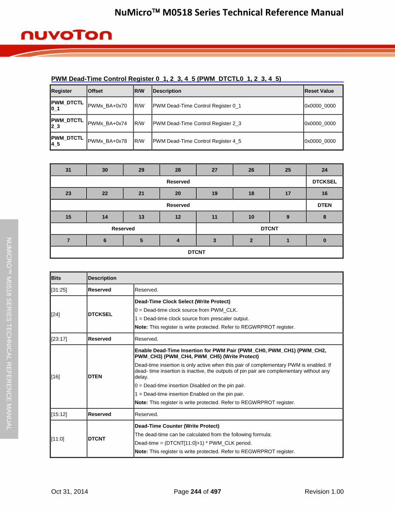
NuMicro M0518 Series Technical Reference Manual
Oct 31, 2014 Page 244 of 497 Revision 1.00
NU
MIC
RO
™ M
0518
SE
RIE
S T
EC
HN
ICA
L R
EF
ER
EN
CE
MA
NU
AL
PWM Dead-Time Control Register 0_1, 2_3, 4_5 (PWM_DTCTL0_1, 2_3, 4_5)
Register Offset R/W Description Reset Value
PWM_DTCTL0_1
PWMx_BA+0x70 R/W PWM Dead-Time Control Register 0_1 0x0000_0000
PWM_DTCTL2_3
PWMx_BA+0x74 R/W PWM Dead-Time Control Register 2_3 0x0000_0000
PWM_DTCTL4_5
PWMx_BA+0x78 R/W PWM Dead-Time Control Register 4_5 0x0000_0000
31 30 29 28 27 26 25 24
Reserved DTCKSEL
23 22 21 20 19 18 17 16
Reserved DTEN
15 14 13 12 11 10 9 8
Reserved DTCNT
7 6 5 4 3 2 1 0
DTCNT
Bits Description
[31:25] Reserved Reserved.
[24] DTCKSEL
Dead-Time Clock Select (Write Protect)
0 = Dead-time clock source from PWM_CLK.
1 = Dead-time clock source from prescaler output.
Note: This register is write protected. Refer to REGWRPROT register.
[23:17] Reserved Reserved.
[16] DTEN
Enable Dead-Time Insertion for PWM Pair (PWM_CH0, PWM_CH1) (PWM_CH2, PWM_CH3) (PWM_CH4, PWM_CH5) (Write Protect)
Dead-time insertion is only active when this pair of complementary PWM is enabled. If dead- time insertion is inactive, the outputs of pin pair are complementary without any delay.
0 = Dead-time insertion Disabled on the pin pair.
1 = Dead-time insertion Enabled on the pin pair.
Note: This register is write protected. Refer to REGWRPROT register.
[15:12] Reserved Reserved.
[11:0] DTCNT
Dead-Time Counter (Write Protect)
The dead-time can be calculated from the following formula:
Dead-time = (DTCNT[11:0]+1) * PWM_CLK period.
Note: This register is write protected. Refer to REGWRPROT register.
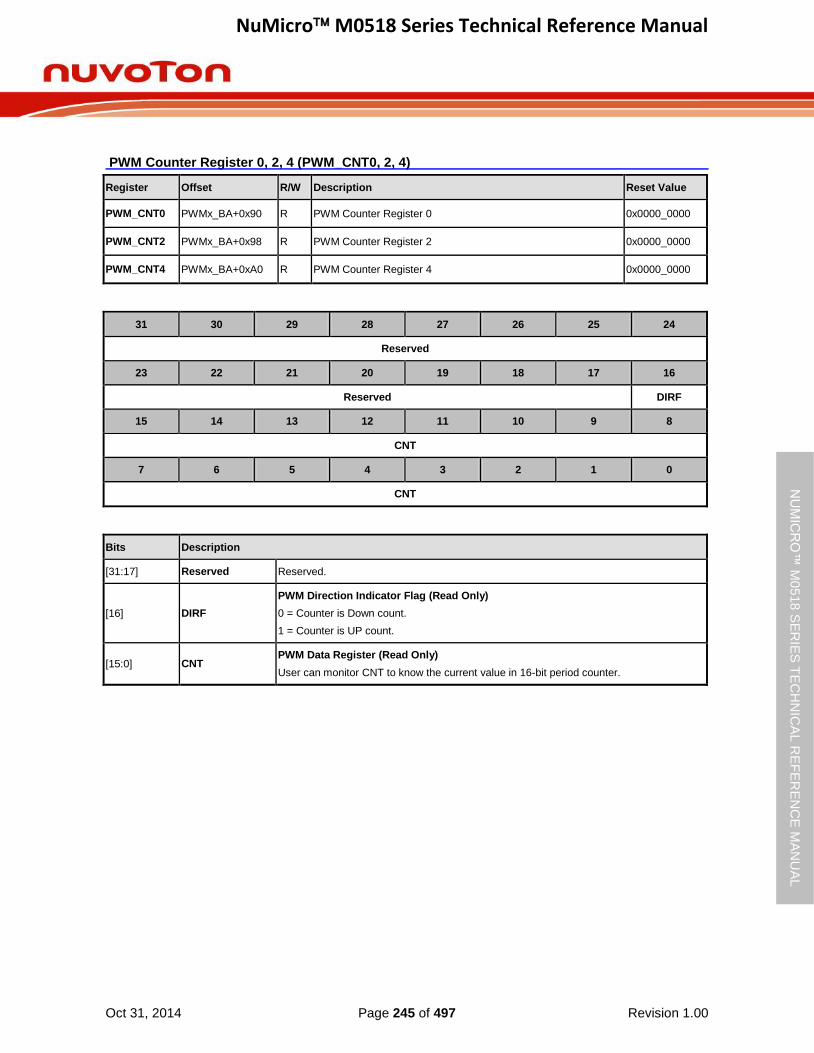
NuMicro M0518 Series Technical Reference Manual
Oct 31, 2014 Page 245 of 497 Revision 1.00
NU
MIC
RO
™ M
0518
SE
RIE
S T
EC
HN
ICA
L R
EF
ER
EN
CE
MA
NU
AL
PWM Counter Register 0, 2, 4 (PWM_CNT0, 2, 4)
Register Offset R/W Description Reset Value
PWM_CNT0 PWMx_BA+0x90 R PWM Counter Register 0 0x0000_0000
PWM_CNT2 PWMx_BA+0x98 R PWM Counter Register 2 0x0000_0000
PWM_CNT4 PWMx_BA+0xA0 R PWM Counter Register 4 0x0000_0000
31 30 29 28 27 26 25 24
Reserved
23 22 21 20 19 18 17 16
Reserved DIRF
15 14 13 12 11 10 9 8
CNT
7 6 5 4 3 2 1 0
CNT
Bits Description
[31:17] Reserved Reserved.
[16] DIRF
PWM Direction Indicator Flag (Read Only)
0 = Counter is Down count.
1 = Counter is UP count.
[15:0] CNT PWM Data Register (Read Only)
User can monitor CNT to know the current value in 16-bit period counter.
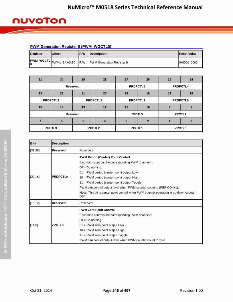
NuMicro M0518 Series Technical Reference Manual
Oct 31, 2014 Page 246 of 497 Revision 1.00
NU
MIC
RO
™ M
0518
SE
RIE
S T
EC
HN
ICA
L R
EF
ER
EN
CE
MA
NU
AL
PWM Generation Register 0 (PWM_WGCTL0)
Register Offset R/W Description Reset Value
PWM_WGCTL0
PWMx_BA+0xB0 R/W PWM Generation Register 0 0x0000_0000
31 30 29 28 27 26 25 24
Reserved PRDPCTL5 PRDPCTL4
23 22 21 20 19 18 17 16
PRDPCTL3 PRDPCTL2 PRDPCTL1 PRDPCTL0
15 14 13 12 11 10 9 8
Reserved ZPCTL5 ZPCTL4
7 6 5 4 3 2 1 0
ZPCTL3 ZPCTL2 ZPCTL1 ZPCTL0
Bits Description
[31:28] Reserved Reserved.
[27:16] PRDPCTLn
PWM Period (Center) Point Control
Each bit n controls the corresponding PWM channel n.
00 = Do nothing.
01 = PWM period (center) point output Low.
10 = PWM period (center) point output High.
11 = PWM period (center) point output Toggle.
PWM can control output level when PWM counter count to (PERIODn+1).
Note: This bit is center point control when PWM counter operating in up-down counter type.
[15:12] Reserved Reserved.
[11:0] ZPCTLn
PWM Zero Point Control
Each bit n controls the corresponding PWM channel n.
00 = Do nothing.
01 = PWM zero point output Low.
10 = PWM zero point output High.
11 = PWM zero point output Toggle.
PWM can control output level when PWM counter count to zero.
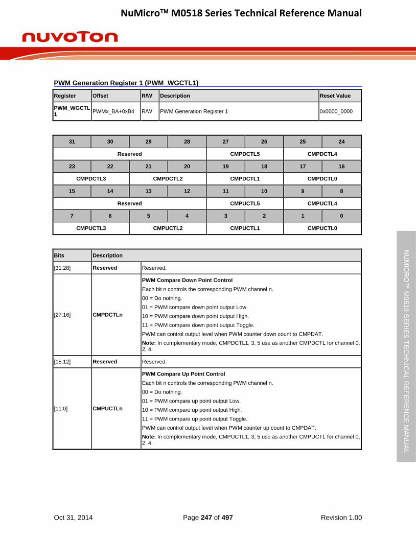
NuMicro M0518 Series Technical Reference Manual
Oct 31, 2014 Page 247 of 497 Revision 1.00
NU
MIC
RO
™ M
0518
SE
RIE
S T
EC
HN
ICA
L R
EF
ER
EN
CE
MA
NU
AL
PWM Generation Register 1 (PWM_WGCTL1)
Register Offset R/W Description Reset Value
PWM_WGCTL1
PWMx_BA+0xB4 R/W PWM Generation Register 1 0x0000_0000
31 30 29 28 27 26 25 24
Reserved CMPDCTL5 CMPDCTL4
23 22 21 20 19 18 17 16
CMPDCTL3 CMPDCTL2 CMPDCTL1 CMPDCTL0
15 14 13 12 11 10 9 8
Reserved CMPUCTL5 CMPUCTL4
7 6 5 4 3 2 1 0
CMPUCTL3 CMPUCTL2 CMPUCTL1 CMPUCTL0
Bits Description
[31:28] Reserved Reserved.
[27:16] CMPDCTLn
PWM Compare Down Point Control
Each bit n controls the corresponding PWM channel n.
00 = Do nothing.
01 = PWM compare down point output Low.
10 = PWM compare down point output High.
11 = PWM compare down point output Toggle.
PWM can control output level when PWM counter down count to CMPDAT.
Note: In complementary mode, CMPDCTL1, 3, 5 use as another CMPDCTL for channel 0, 2, 4.
[15:12] Reserved Reserved.
[11:0] CMPUCTLn
PWM Compare Up Point Control
Each bit n controls the corresponding PWM channel n.
00 = Do nothing.
01 = PWM compare up point output Low.
10 = PWM compare up point output High.
11 = PWM compare up point output Toggle.
PWM can control output level when PWM counter up count to CMPDAT.
Note: In complementary mode, CMPUCTL1, 3, 5 use as another CMPUCTL for channel 0, 2, 4.

NuMicro M0518 Series Technical Reference Manual
Oct 31, 2014 Page 248 of 497 Revision 1.00
NU
MIC
RO
™ M
0518
SE
RIE
S T
EC
HN
ICA
L R
EF
ER
EN
CE
MA
NU
AL
PWM Mask Enable Register (PWM_MSKEN)
Register Offset R/W Description Reset Value
PWM_MSKEN PWMx_BA+0xB8 R/W PWM Mask Enable Register 0x0000_0000
31 30 29 28 27 26 25 24
Reserved
23 22 21 20 19 18 17 16
Reserved
15 14 13 12 11 10 9 8
Reserved
7 6 5 4 3 2 1 0
Reserved MSKEN5 MSKEN4 MSKEN3 MSKEN2 MSKEN1 MSKEN0
Bits Description
[31:6] Reserved Reserved.
[5:0] MSKENn
PWM Mask Enable Control
Each bit n controls the corresponding PWM channel n.
The PWM output signal will be masked when this bit is enabled. The corresponding PWM channel n will output MSKDATn (PWM_MSK[5:0]) data.
0 = PWM output signal is non-masked.
1 = PWM output signal is masked and output MSKDATn data.
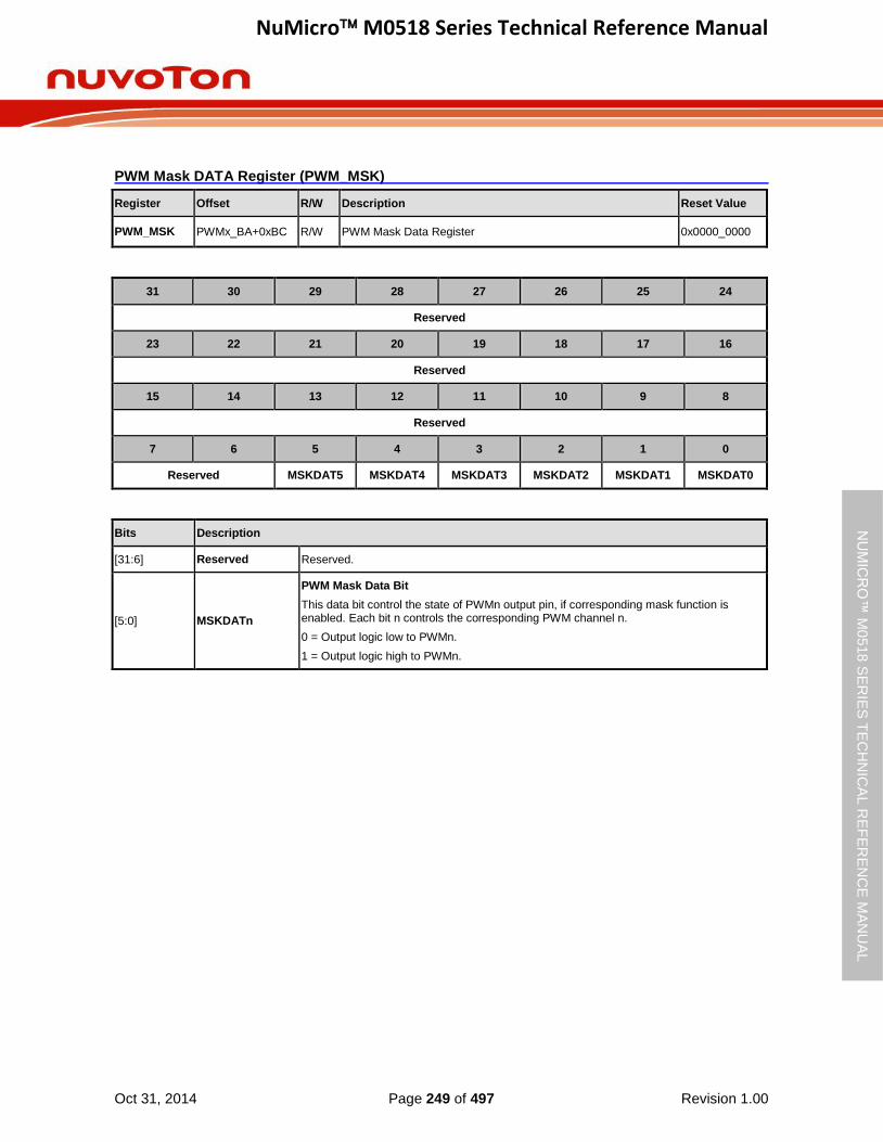
NuMicro M0518 Series Technical Reference Manual
Oct 31, 2014 Page 249 of 497 Revision 1.00
NU
MIC
RO
™ M
0518
SE
RIE
S T
EC
HN
ICA
L R
EF
ER
EN
CE
MA
NU
AL
PWM Mask DATA Register (PWM_MSK)
Register Offset R/W Description Reset Value
PWM_MSK PWMx_BA+0xBC R/W PWM Mask Data Register 0x0000_0000
31 30 29 28 27 26 25 24
Reserved
23 22 21 20 19 18 17 16
Reserved
15 14 13 12 11 10 9 8
Reserved
7 6 5 4 3 2 1 0
Reserved MSKDAT5 MSKDAT4 MSKDAT3 MSKDAT2 MSKDAT1 MSKDAT0
Bits Description
[31:6] Reserved Reserved.
[5:0] MSKDATn
PWM Mask Data Bit
This data bit control the state of PWMn output pin, if corresponding mask function is enabled. Each bit n controls the corresponding PWM channel n.
0 = Output logic low to PWMn.
1 = Output logic high to PWMn.
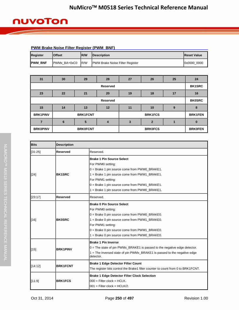
NuMicro M0518 Series Technical Reference Manual
Oct 31, 2014 Page 250 of 497 Revision 1.00
NU
MIC
RO
™ M
0518
SE
RIE
S T
EC
HN
ICA
L R
EF
ER
EN
CE
MA
NU
AL
PWM Brake Noise Filter Register (PWM_BNF)
Register Offset R/W Description Reset Value
PWM_BNF PWMx_BA+0xC0 R/W PWM Brake Noise Filter Register 0x0000_0000
31 30 29 28 27 26 25 24
Reserved BK1SRC
23 22 21 20 19 18 17 16
Reserved BK0SRC
15 14 13 12 11 10 9 8
BRK1PINV BRK1FCNT BRK1FCS BRK1FEN
7 6 5 4 3 2 1 0
BRK0PINV BRK0FCNT BRK0FCS BRK0FEN
Bits Description
[31:25] Reserved Reserved.
[24] BK1SRC
Brake 1 Pin Source Select
For PWM0 setting:
0 = Brake 1 pin source come from PWM0_BRAKE1.
1 = Brake 1 pin source come from PWM1_BRAKE1.
For PWM1 setting:
0 = Brake 1 pin source come from PWM1_BRAKE1.
1 = Brake 1 pin source come from PWM0_BRAKE1.
[23:17] Reserved Reserved.
[16] BK0SRC
Brake 0 Pin Source Select
For PWM0 setting:
0 = Brake 0 pin source come from PWM0_BRAKE0.
1 = Brake 0 pin source come from PWM1_BRAKE0.
For PWM1 setting:
0 = Brake 0 pin source come from PWM1_BRAKE0.
1 = Brake 0 pin source come from PWM0_BRAKE0.
[15] BRK1PINV
Brake 1 Pin Inverse
0 = The state of pin PWMx_BRAKE1 is passed to the negative edge detector.
1 = The inversed state of pin PWMx_BRAKE1 is passed to the negative edge detector.
[14:12] BRK1FCNT Brake 1 Edge Detector Filter Count
The register bits control the Brake1 filter counter to count from 0 to BRK1FCNT.
[11:9] BRK1FCS
Brake 1 Edge Detector Filter Clock Selection
000 = Filter clock = HCLK.
001 = Filter clock = HCLK/2.

NuMicro M0518 Series Technical Reference Manual
Oct 31, 2014 Page 251 of 497 Revision 1.00
NU
MIC
RO
™ M
0518
SE
RIE
S T
EC
HN
ICA
L R
EF
ER
EN
CE
MA
NU
AL
010 = Filter clock = HCLK/4.
011 = Filter clock = HCLK/8.
100 = Filter clock = HCLK/16.
101 = Filter clock = HCLK/32.
110 = Filter clock = HCLK/64.
111 = Filter clock = HCLK/128.
[8] BRK1FEN
PWM Brake 1 Noise Filter Enable Control
0 = Noise filter of PWM Brake 1 Disabled.
1 = Noise filter of PWM Brake 1 Enabled.
[7] BRK0PINV
Brake 0 Pin Inverse
0 = The state of pin PWMx_BRAKE0 is passed to the negative edge detector.
1 = The inversed state of pin PWMx_BRAKE10 is passed to the negative edge detector.
[6:4] BRK0FCNT Brake 0 Edge Detector Filter Count
The register bits control the Brake0 filter counter to count from 0 to BRK1FCNT.
[3:1] BRK0FCS
Brake 0 Edge Detector Filter Clock Selection
000 = Filter clock is HCLK.
001 = Filter clock is HCLK/2.
010 = Filter clock is HCLK/4.
011 = Filter clock is HCLK/8.
100 = Filter clock is HCLK/16.
101 = Filter clock is HCLK/32.
110 = Filter clock is HCLK/64.
111 = Filter clock is HCLK/128.
[0] BRK0FEN
PWM Brake 0 Noise Filter Enable Control
0 = Noise filter of PWM Brake 0 Disabled.
1 = Noise filter of PWM Brake 0 Enabled.

NuMicro M0518 Series Technical Reference Manual
Oct 31, 2014 Page 252 of 497 Revision 1.00
NU
MIC
RO
™ M
0518
SE
RIE
S T
EC
HN
ICA
L R
EF
ER
EN
CE
MA
NU
AL
PWM System Fail Brake Control Register (PWM_FAILBRK)
Register Offset R/W Description Reset Value
PWM_FAILBRK
PWMx_BA+0xC4 R/W PWM System Fail Brake Control Register 0x0000_0000
31 30 29 28 27 26 25 24
Reserved
23 22 21 20 19 18 17 16
Reserved
15 14 13 12 11 10 9 8
Reserved
7 6 5 4 3 2 1 0
Reserved CORBRKEN Reserved BODBRKEN CSSBRKEN
Bits Description
[31:4] Reserved Reserved.
[3] CORBRKEN
Core Lockup Detection Trigger PWM Brake Function 0 Enable Control
0 = Brake Function triggered by Core lockup detection Disabled.
1 = Brake Function triggered by Core lockup detection Enabled.
[2] Reserved Reserved.
[1] BODBRKEN
Brown-Out Detection Trigger PWM Brake Function 0 Enable
0 = Brake Function triggered by BOD Disabled.
1 = Brake Function triggered by BOD Enabled.
[0] CSSBRKEN
Clock Security System Detection Trigger PWM Brake Function 0 Enable Control
0 = Brake Function triggered by CSS detection Disabled.
1 = Brake Function triggered by CSS detection Enabled.

NuMicro M0518 Series Technical Reference Manual
Oct 31, 2014 Page 253 of 497 Revision 1.00
NU
MIC
RO
™ M
0518
SE
RIE
S T
EC
HN
ICA
L R
EF
ER
EN
CE
MA
NU
AL
PWM Brake Edge Detect Control Register 0_1, 2_3, 4_5(PWM_BRKCTL0_1, 2_3, 4_5)
Register Offset R/W Description Reset Value
PWM_BRKCTL0_1
PWMx_BA+0xC8 R/W PWM Brake Edge Detect Control Register 0_1 0x0000_0000
PWM_BRKCTL2_3
PWMx_BA+0xCC R/W PWM Brake Edge Detect Control Register 2_3 0x0000_0000
PWM_BRKCTL4_5
PWMx_BA+0xD0 R/W PWM Brake Edge Detect Control Register 4_5 0x0000_0000
31 30 29 28 27 26 25 24
Reserved
23 22 21 20 19 18 17 16
Reserved BRKAODD BRKAEVEN
15 14 13 12 11 10 9 8
SYSLEN Reserved BRKP1LEN BRKP0LEN Reserved
7 6 5 4 3 2 1 0
SYSEEN Reserved BRKP1EEN BRKP0EEN Reserved
Bits Description
[31:20] Reserved Reserved.
[19:18] BRKAODD
PWM Brake Action Select For Odd Channel (Write Protect)
00 = PWM odd channel level-detect brake function not affect channel output.
01 = PWM odd channel output tri-state when level-detect brake happened.
10 = PWM odd channel output low level when level-detect brake happened.
11 = PWM odd channel output high level when level-detect brake happened.
Note: This register is write protected. Refer to REGWRPROT register.
[17:16] BRKAEVEN
PWM Brake Action Select For Even Channel (Write Protect)
00 = PWM even channel level-detect brake function not affect channel output.
01 = PWM even channel output tri-state when level-detect brake happened.
10 = PWM even channel output low level when level-detect brake happened.
11 = PWM even channel output high level when level-detect brake happened.
Note: This register is write protected. Refer to REGWRPROT register.
[15] SYSLEN
Enable System Fail As Level-Detect Brake Source (Write Protect)
0 = System Fail condition as level-detect brake source Disabled.
1 = System Fail condition as level-detect brake source Enabled.
Note: This register is write protected. Refer to REGWRPROT register.
[14] Reserved Reserved.
[13] BRKP1LEN Enable BKP1 Pin As Level-Detect Brake Source (Write Protect)
0 = PWMx_BRAKE1 pin as level-detect brake source Disabled.
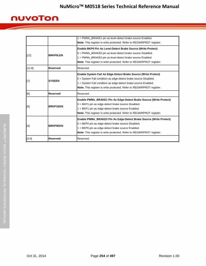
NuMicro M0518 Series Technical Reference Manual
Oct 31, 2014 Page 254 of 497 Revision 1.00
NU
MIC
RO
™ M
0518
SE
RIE
S T
EC
HN
ICA
L R
EF
ER
EN
CE
MA
NU
AL
1 = PWMx_BRAKE1 pin as level-detect brake source Enabled.
Note: This register is write protected. Refer to REGWRPROT register.
[12] BRKP0LEN
Enable BKP0 Pin As Level-Detect Brake Source (Write Protect)
0 = PWMx_BRAKE0 pin as level-detect brake source Disabled.
1 = PWMx_BRAKE0 pin as level-detect brake source Enabled.
Note: This register is write protected. Refer to REGWRPROT register.
[11:8] Reserved Reserved.
[7] SYSEEN
Enable System Fail As Edge-Detect Brake Source (Write Protect)
0 = System Fail condition as edge-detect brake source Disabled.
1 = System Fail condition as edge-detect brake source Enabled.
Note: This register is write protected. Refer to REGWRPROT register.
[6] Reserved Reserved.
[5] BRKP1EEN
Enable PWMx_BRAKE1 Pin As Edge-Detect Brake Source (Write Protect)
0 = BKP1 pin as edge-detect brake source Disabled.
1 = BKP1 pin as edge-detect brake source Enabled.
Note: This register is write protected. Refer to REGWRPROT register.
[4] BRKP0EEN
Enable PWMx_BRAKE0 Pin As Edge-Detect Brake Source (Write Protect)
0 = BKP0 pin as edge-detect brake source Disabled.
1 = BKP0 pin as edge-detect brake source Enabled.
Note: This register is write protected. Refer to REGWRPROT register.
[3:0] Reserved Reserved.

NuMicro M0518 Series Technical Reference Manual
Oct 31, 2014 Page 255 of 497 Revision 1.00
NU
MIC
RO
™ M
0518
SE
RIE
S T
EC
HN
ICA
L R
EF
ER
EN
CE
MA
NU
AL
PWM Pin Polar Inverse Control (PWM_POLCTL)
Register Offset R/W Description Reset Value
PWM_POLCTL
PWMx_BA+0xD4 R/W PWM Pin Polar Inverse Register 0x0000_0000
31 30 29 28 27 26 25 24
Reserved
23 22 21 20 19 18 17 16
Reserved
15 14 13 12 11 10 9 8
Reserved
7 6 5 4 3 2 1 0
Reserved PINV5 PINV4 PINV3 PINV2 PINV1 PINV0
Bits Description
[31:6] Reserved Reserved.
[5:0] PINVn
PWM PIN Polar Inverse Control
The register controls polarity state of PWM output. Each bit n controls the corresponding PWM channel n.
0 = PWM output polar inverse Disabled.
1 = PWM output polar inverse Enabled.
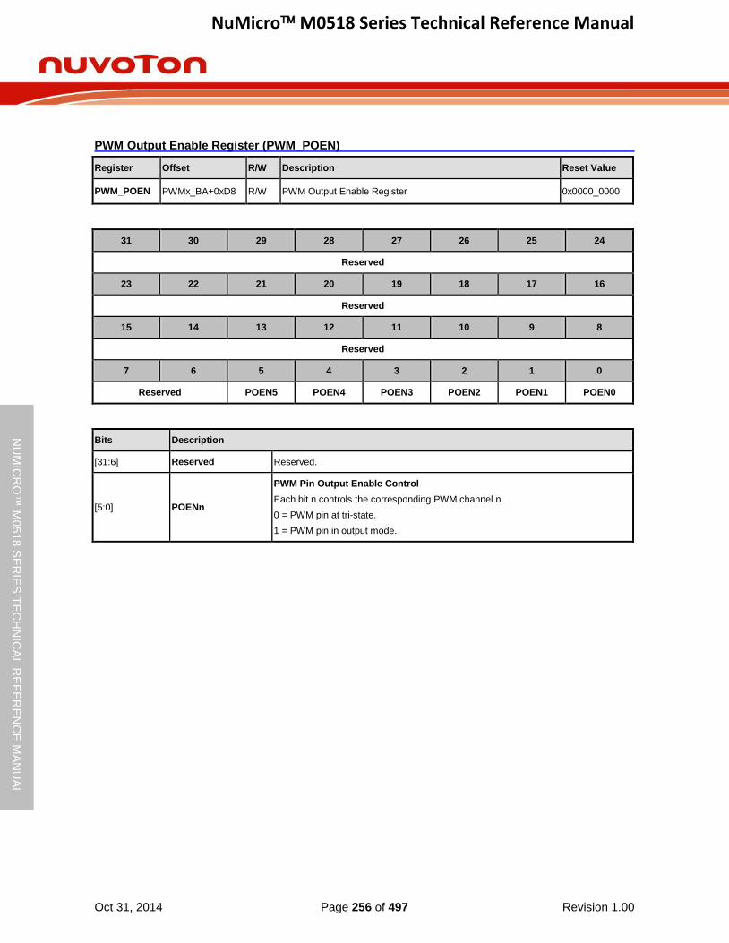
NuMicro M0518 Series Technical Reference Manual
Oct 31, 2014 Page 256 of 497 Revision 1.00
NU
MIC
RO
™ M
0518
SE
RIE
S T
EC
HN
ICA
L R
EF
ER
EN
CE
MA
NU
AL
PWM Output Enable Register (PWM_POEN)
Register Offset R/W Description Reset Value
PWM_POEN PWMx_BA+0xD8 R/W PWM Output Enable Register 0x0000_0000
31 30 29 28 27 26 25 24
Reserved
23 22 21 20 19 18 17 16
Reserved
15 14 13 12 11 10 9 8
Reserved
7 6 5 4 3 2 1 0
Reserved POEN5 POEN4 POEN3 POEN2 POEN1 POEN0
Bits Description
[31:6] Reserved Reserved.
[5:0] POENn
PWM Pin Output Enable Control
Each bit n controls the corresponding PWM channel n.
0 = PWM pin at tri-state.
1 = PWM pin in output mode.
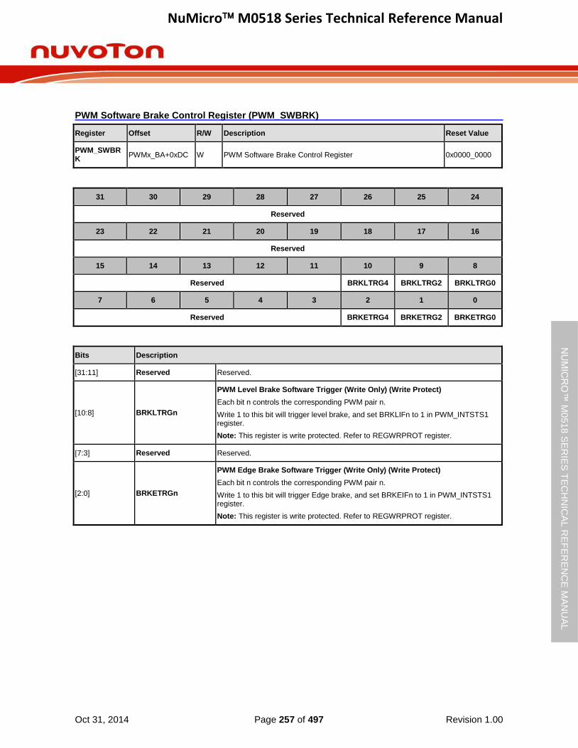
NuMicro M0518 Series Technical Reference Manual
Oct 31, 2014 Page 257 of 497 Revision 1.00
NU
MIC
RO
™ M
0518
SE
RIE
S T
EC
HN
ICA
L R
EF
ER
EN
CE
MA
NU
AL
PWM Software Brake Control Register (PWM_SWBRK)
Register Offset R/W Description Reset Value
PWM_SWBRK
PWMx_BA+0xDC W PWM Software Brake Control Register 0x0000_0000
31 30 29 28 27 26 25 24
Reserved
23 22 21 20 19 18 17 16
Reserved
15 14 13 12 11 10 9 8
Reserved BRKLTRG4 BRKLTRG2 BRKLTRG0
7 6 5 4 3 2 1 0
Reserved BRKETRG4 BRKETRG2 BRKETRG0
Bits Description
[31:11] Reserved Reserved.
[10:8] BRKLTRGn
PWM Level Brake Software Trigger (Write Only) (Write Protect)
Each bit n controls the corresponding PWM pair n.
Write 1 to this bit will trigger level brake, and set BRKLIFn to 1 in PWM_INTSTS1 register.
Note: This register is write protected. Refer to REGWRPROT register.
[7:3] Reserved Reserved.
[2:0] BRKETRGn
PWM Edge Brake Software Trigger (Write Only) (Write Protect)
Each bit n controls the corresponding PWM pair n.
Write 1 to this bit will trigger Edge brake, and set BRKEIFn to 1 in PWM_INTSTS1 register.
Note: This register is write protected. Refer to REGWRPROT register.
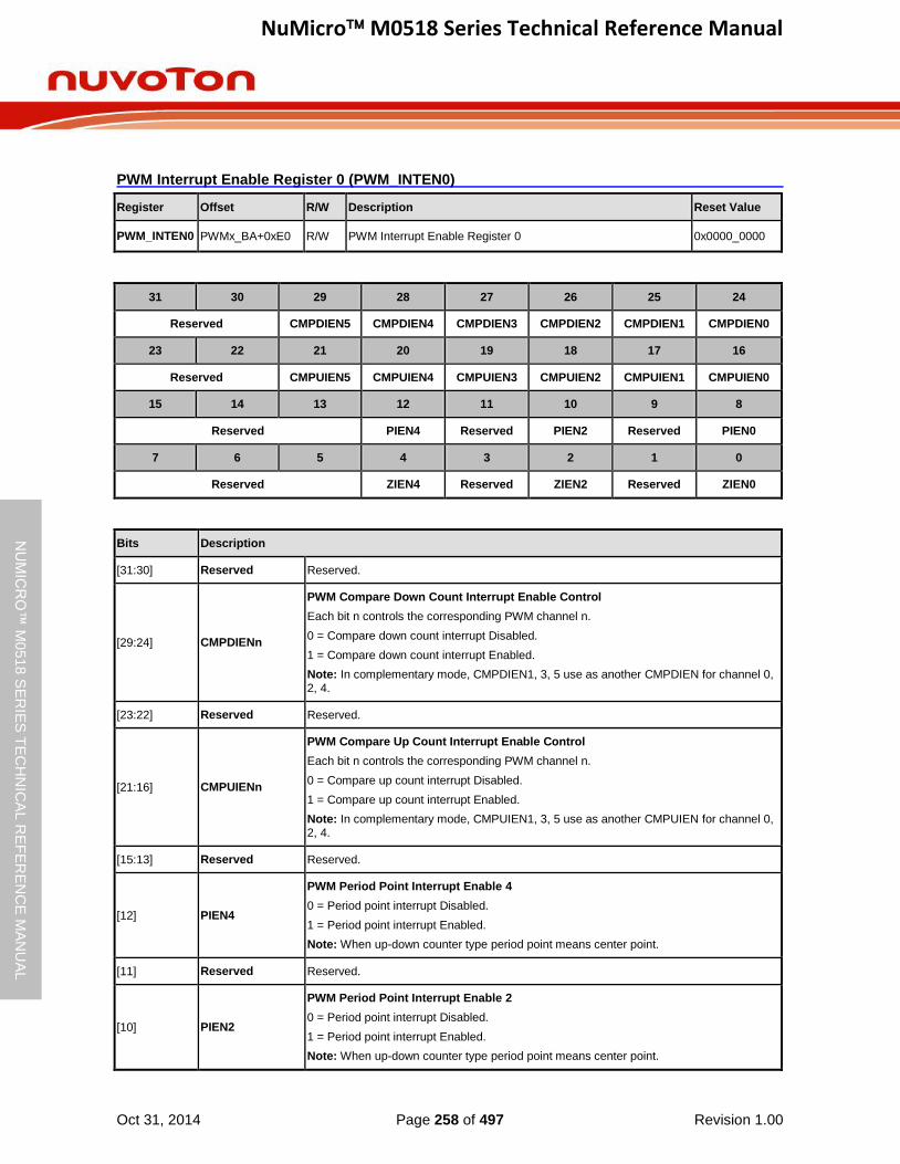
NuMicro M0518 Series Technical Reference Manual
Oct 31, 2014 Page 258 of 497 Revision 1.00
NU
MIC
RO
™ M
0518
SE
RIE
S T
EC
HN
ICA
L R
EF
ER
EN
CE
MA
NU
AL
PWM Interrupt Enable Register 0 (PWM_INTEN0)
Register Offset R/W Description Reset Value
PWM_INTEN0 PWMx_BA+0xE0 R/W PWM Interrupt Enable Register 0 0x0000_0000
31 30 29 28 27 26 25 24
Reserved CMPDIEN5 CMPDIEN4 CMPDIEN3 CMPDIEN2 CMPDIEN1 CMPDIEN0
23 22 21 20 19 18 17 16
Reserved CMPUIEN5 CMPUIEN4 CMPUIEN3 CMPUIEN2 CMPUIEN1 CMPUIEN0
15 14 13 12 11 10 9 8
Reserved PIEN4 Reserved PIEN2 Reserved PIEN0
7 6 5 4 3 2 1 0
Reserved ZIEN4 Reserved ZIEN2 Reserved ZIEN0
Bits Description
[31:30] Reserved Reserved.
[29:24] CMPDIENn
PWM Compare Down Count Interrupt Enable Control
Each bit n controls the corresponding PWM channel n.
0 = Compare down count interrupt Disabled.
1 = Compare down count interrupt Enabled.
Note: In complementary mode, CMPDIEN1, 3, 5 use as another CMPDIEN for channel 0, 2, 4.
[23:22] Reserved Reserved.
[21:16] CMPUIENn
PWM Compare Up Count Interrupt Enable Control
Each bit n controls the corresponding PWM channel n.
0 = Compare up count interrupt Disabled.
1 = Compare up count interrupt Enabled.
Note: In complementary mode, CMPUIEN1, 3, 5 use as another CMPUIEN for channel 0, 2, 4.
[15:13] Reserved Reserved.
[12] PIEN4
PWM Period Point Interrupt Enable 4
0 = Period point interrupt Disabled.
1 = Period point interrupt Enabled.
Note: When up-down counter type period point means center point.
[11] Reserved Reserved.
[10] PIEN2
PWM Period Point Interrupt Enable 2
0 = Period point interrupt Disabled.
1 = Period point interrupt Enabled.
Note: When up-down counter type period point means center point.
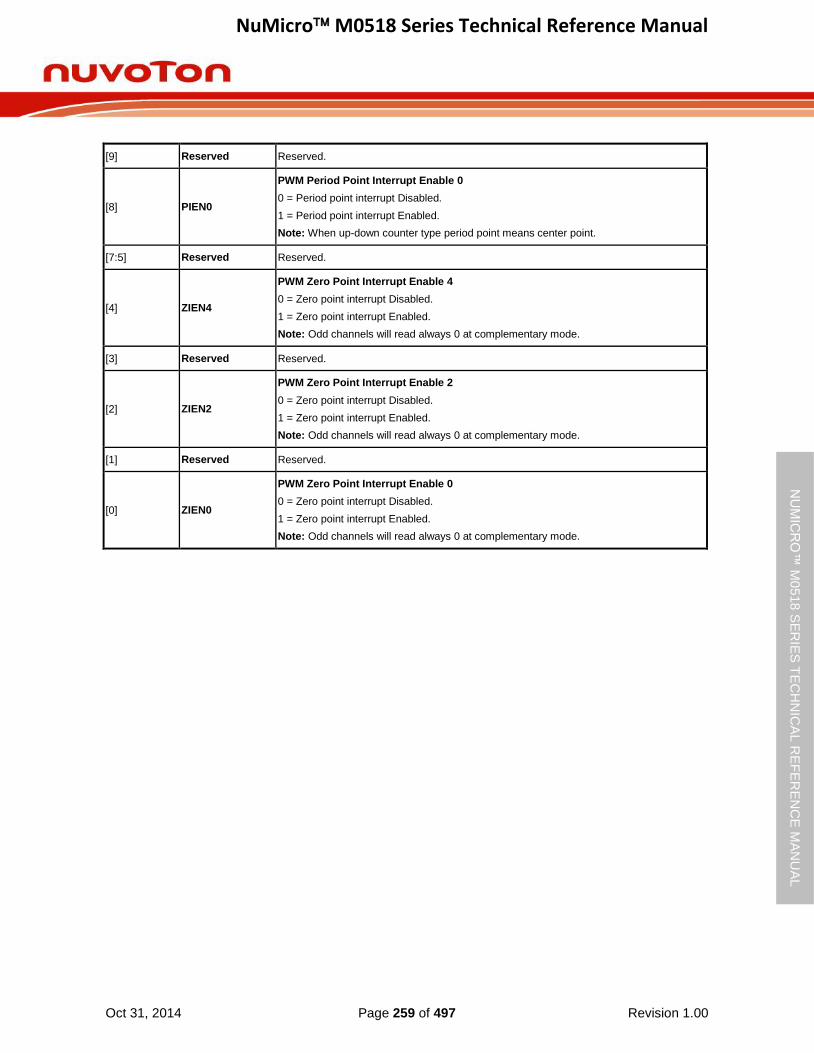
NuMicro M0518 Series Technical Reference Manual
Oct 31, 2014 Page 259 of 497 Revision 1.00
NU
MIC
RO
™ M
0518
SE
RIE
S T
EC
HN
ICA
L R
EF
ER
EN
CE
MA
NU
AL
[9] Reserved Reserved.
[8] PIEN0
PWM Period Point Interrupt Enable 0
0 = Period point interrupt Disabled.
1 = Period point interrupt Enabled.
Note: When up-down counter type period point means center point.
[7:5] Reserved Reserved.
[4] ZIEN4
PWM Zero Point Interrupt Enable 4
0 = Zero point interrupt Disabled.
1 = Zero point interrupt Enabled.
Note: Odd channels will read always 0 at complementary mode.
[3] Reserved Reserved.
[2] ZIEN2
PWM Zero Point Interrupt Enable 2
0 = Zero point interrupt Disabled.
1 = Zero point interrupt Enabled.
Note: Odd channels will read always 0 at complementary mode.
[1] Reserved Reserved.
[0] ZIEN0
PWM Zero Point Interrupt Enable 0
0 = Zero point interrupt Disabled.
1 = Zero point interrupt Enabled.
Note: Odd channels will read always 0 at complementary mode.
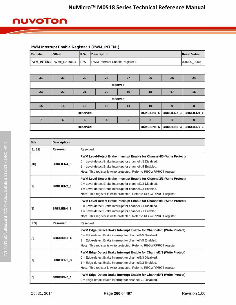
NuMicro M0518 Series Technical Reference Manual
Oct 31, 2014 Page 260 of 497 Revision 1.00
NU
MIC
RO
™ M
0518
SE
RIE
S T
EC
HN
ICA
L R
EF
ER
EN
CE
MA
NU
AL
PWM Interrupt Enable Register 1 (PWM_INTEN1)
Register Offset R/W Description Reset Value
PWM_INTEN1 PWMx_BA+0xE4 R/W PWM Interrupt Enable Register 1 0x0000_0000
31 30 29 28 27 26 25 24
Reserved
23 22 21 20 19 18 17 16
Reserved
15 14 13 12 11 10 9 8
Reserved BRKLIEN4_5 BRKLIEN2_3 BRKLIEN0_1
7 6 5 4 3 2 1 0
Reserved BRKEIEN4_5 BRKEIEN2_3 BRKEIEN0_1
Bits Description
[31:11] Reserved Reserved.
[10] BRKLIEN4_5
PWM Level-Detect Brake Interrupt Enable for Channel4/5 (Write Protect)
0 = Level-detect Brake interrupt for channel4/5 Disabled.
1 = Level-detect Brake interrupt for channel4/5 Enabled.
Note: This register is write protected. Refer to REGWRPROT register.
[9] BRKLIEN2_3
PWM Level-Detect Brake Interrupt Enable for Channel2/3 (Write Protect)
0 = Level-detect Brake interrupt for channel2/3 Disabled.
1 = Level-detect Brake interrupt for channel2/3 Enabled.
Note: This register is write protected. Refer to REGWRPROT register.
[8] BRKLIEN0_1
PWM Level-Detect Brake Interrupt Enable for Channel0/1 (Write Protect)
0 = Level-detect Brake interrupt for channel0/1 Disabled.
1 = Level-detect Brake interrupt for channel0/1 Enabled.
Note: This register is write protected. Refer to REGWRPROT register.
[7:3] Reserved Reserved.
[2] BRKEIEN4_5
PWM Edge-Detect Brake Interrupt Enable for Channel4/5 (Write Protect)
0 = Edge-detect Brake interrupt for channel4/5 Disabled.
1 = Edge-detect Brake interrupt for channel4/5 Enabled.
Note: This register is write protected. Refer to REGWRPROT register.
[1] BRKEIEN2_3
PWM Edge-Detect Brake Interrupt Enable for Channel2/3 (Write Protect)
0 = Edge-detect Brake interrupt for channel2/3 Disabled.
1 = Edge-detect Brake interrupt for channel2/3 Enabled.
Note: This register is write protected. Refer to REGWRPROT register.
[0] BRKEIEN0_1 PWM Edge-Detect Brake Interrupt Enable for Channel0/1 (Write Protect)
0 = Edge-detect Brake interrupt for channel0/1 Disabled.

NuMicro M0518 Series Technical Reference Manual
Oct 31, 2014 Page 261 of 497 Revision 1.00
NU
MIC
RO
™ M
0518
SE
RIE
S T
EC
HN
ICA
L R
EF
ER
EN
CE
MA
NU
AL
1 = Edge-detect Brake interrupt for channel0/1 Enabled.
Note: This register is write protected. Refer to REGWRPROT register.
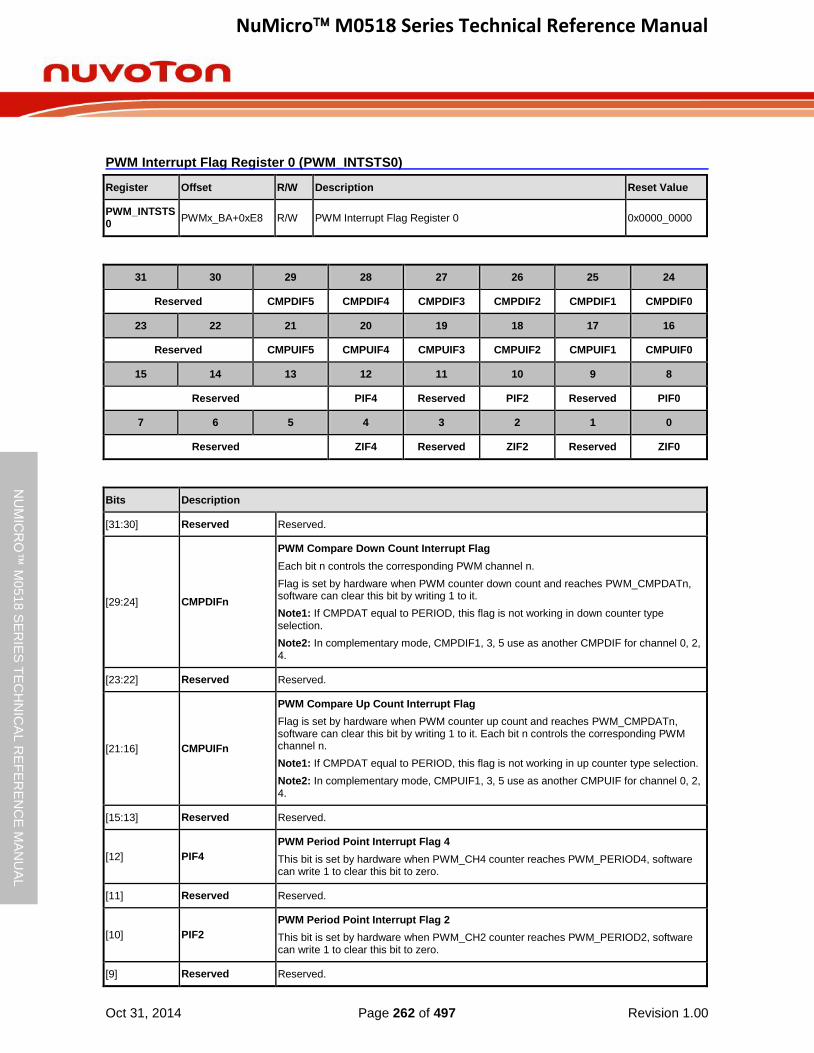
NuMicro M0518 Series Technical Reference Manual
Oct 31, 2014 Page 262 of 497 Revision 1.00
NU
MIC
RO
™ M
0518
SE
RIE
S T
EC
HN
ICA
L R
EF
ER
EN
CE
MA
NU
AL
PWM Interrupt Flag Register 0 (PWM_INTSTS0)
Register Offset R/W Description Reset Value
PWM_INTSTS0
PWMx_BA+0xE8 R/W PWM Interrupt Flag Register 0 0x0000_0000
31 30 29 28 27 26 25 24
Reserved CMPDIF5 CMPDIF4 CMPDIF3 CMPDIF2 CMPDIF1 CMPDIF0
23 22 21 20 19 18 17 16
Reserved CMPUIF5 CMPUIF4 CMPUIF3 CMPUIF2 CMPUIF1 CMPUIF0
15 14 13 12 11 10 9 8
Reserved PIF4 Reserved PIF2 Reserved PIF0
7 6 5 4 3 2 1 0
Reserved ZIF4 Reserved ZIF2 Reserved ZIF0
Bits Description
[31:30] Reserved Reserved.
[29:24] CMPDIFn
PWM Compare Down Count Interrupt Flag
Each bit n controls the corresponding PWM channel n.
Flag is set by hardware when PWM counter down count and reaches PWM_CMPDATn, software can clear this bit by writing 1 to it.
Note1: If CMPDAT equal to PERIOD, this flag is not working in down counter type selection.
Note2: In complementary mode, CMPDIF1, 3, 5 use as another CMPDIF for channel 0, 2, 4.
[23:22] Reserved Reserved.
[21:16] CMPUIFn
PWM Compare Up Count Interrupt Flag
Flag is set by hardware when PWM counter up count and reaches PWM_CMPDATn, software can clear this bit by writing 1 to it. Each bit n controls the corresponding PWM channel n.
Note1: If CMPDAT equal to PERIOD, this flag is not working in up counter type selection.
Note2: In complementary mode, CMPUIF1, 3, 5 use as another CMPUIF for channel 0, 2, 4.
[15:13] Reserved Reserved.
[12] PIF4
PWM Period Point Interrupt Flag 4
This bit is set by hardware when PWM_CH4 counter reaches PWM_PERIOD4, software can write 1 to clear this bit to zero.
[11] Reserved Reserved.
[10] PIF2
PWM Period Point Interrupt Flag 2
This bit is set by hardware when PWM_CH2 counter reaches PWM_PERIOD2, software can write 1 to clear this bit to zero.
[9] Reserved Reserved.
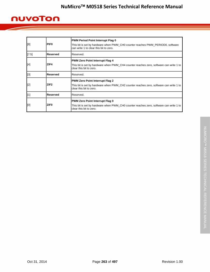
NuMicro M0518 Series Technical Reference Manual
Oct 31, 2014 Page 263 of 497 Revision 1.00
NU
MIC
RO
™ M
0518
SE
RIE
S T
EC
HN
ICA
L R
EF
ER
EN
CE
MA
NU
AL
[8] PIF0
PWM Period Point Interrupt Flag 0
This bit is set by hardware when PWM_CH0 counter reaches PWM_PERIOD0, software can write 1 to clear this bit to zero.
[7:5] Reserved Reserved.
[4] ZIF4
PWM Zero Point Interrupt Flag 4
This bit is set by hardware when PWM_CH4 counter reaches zero, software can write 1 to clear this bit to zero.
[3] Reserved Reserved.
[2] ZIF2
PWM Zero Point Interrupt Flag 2
This bit is set by hardware when PWM_CH2 counter reaches zero, software can write 1 to clear this bit to zero.
[1] Reserved Reserved.
[0] ZIF0
PWM Zero Point Interrupt Flag 0
This bit is set by hardware when PWM_CH0 counter reaches zero, software can write 1 to clear this bit to zero.
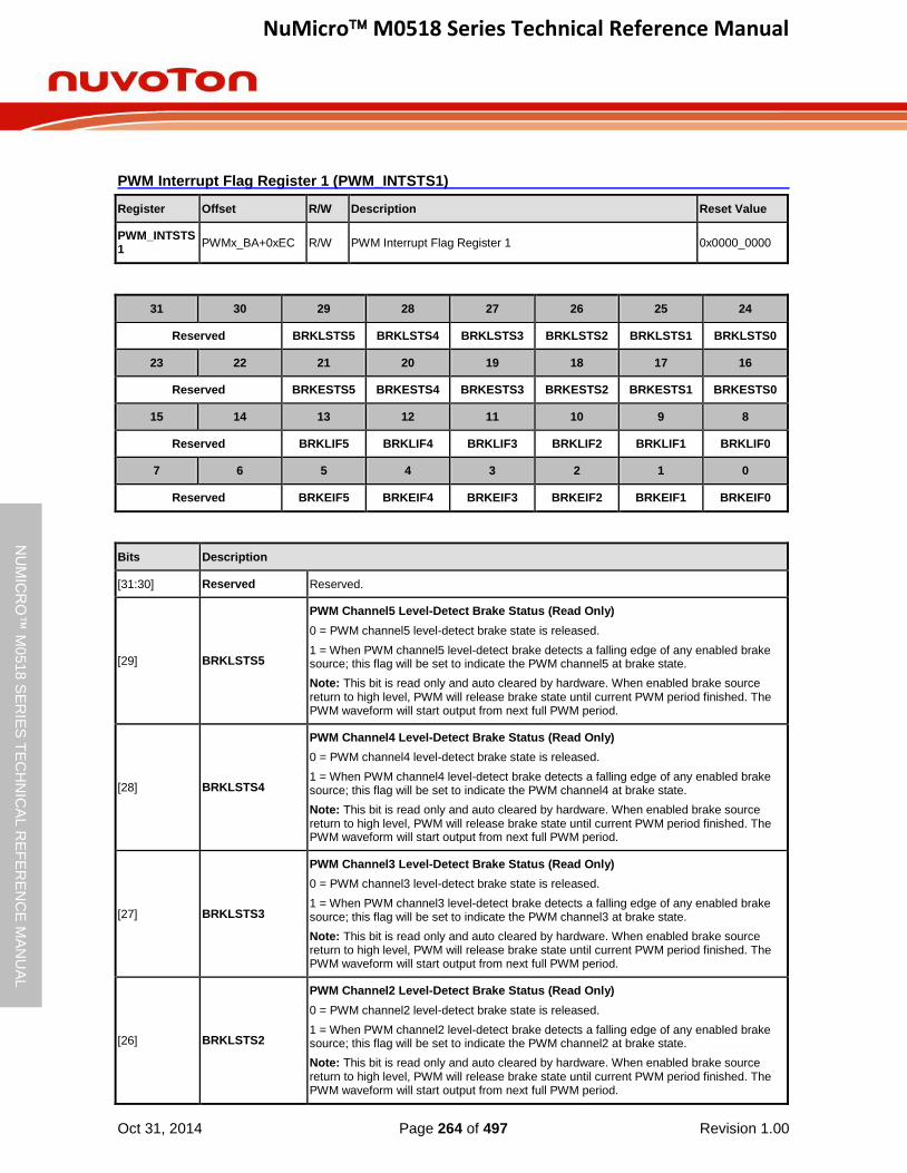
NuMicro M0518 Series Technical Reference Manual
Oct 31, 2014 Page 264 of 497 Revision 1.00
NU
MIC
RO
™ M
0518
SE
RIE
S T
EC
HN
ICA
L R
EF
ER
EN
CE
MA
NU
AL
PWM Interrupt Flag Register 1 (PWM_INTSTS1)
Register Offset R/W Description Reset Value
PWM_INTSTS1
PWMx_BA+0xEC R/W PWM Interrupt Flag Register 1 0x0000_0000
31 30 29 28 27 26 25 24
Reserved BRKLSTS5 BRKLSTS4 BRKLSTS3 BRKLSTS2 BRKLSTS1 BRKLSTS0
23 22 21 20 19 18 17 16
Reserved BRKESTS5 BRKESTS4 BRKESTS3 BRKESTS2 BRKESTS1 BRKESTS0
15 14 13 12 11 10 9 8
Reserved BRKLIF5 BRKLIF4 BRKLIF3 BRKLIF2 BRKLIF1 BRKLIF0
7 6 5 4 3 2 1 0
Reserved BRKEIF5 BRKEIF4 BRKEIF3 BRKEIF2 BRKEIF1 BRKEIF0
Bits Description
[31:30] Reserved Reserved.
[29] BRKLSTS5
PWM Channel5 Level-Detect Brake Status (Read Only)
0 = PWM channel5 level-detect brake state is released.
1 = When PWM channel5 level-detect brake detects a falling edge of any enabled brake source; this flag will be set to indicate the PWM channel5 at brake state.
Note: This bit is read only and auto cleared by hardware. When enabled brake source return to high level, PWM will release brake state until current PWM period finished. The PWM waveform will start output from next full PWM period.
[28] BRKLSTS4
PWM Channel4 Level-Detect Brake Status (Read Only)
0 = PWM channel4 level-detect brake state is released.
1 = When PWM channel4 level-detect brake detects a falling edge of any enabled brake source; this flag will be set to indicate the PWM channel4 at brake state.
Note: This bit is read only and auto cleared by hardware. When enabled brake source return to high level, PWM will release brake state until current PWM period finished. The PWM waveform will start output from next full PWM period.
[27] BRKLSTS3
PWM Channel3 Level-Detect Brake Status (Read Only)
0 = PWM channel3 level-detect brake state is released.
1 = When PWM channel3 level-detect brake detects a falling edge of any enabled brake source; this flag will be set to indicate the PWM channel3 at brake state.
Note: This bit is read only and auto cleared by hardware. When enabled brake source return to high level, PWM will release brake state until current PWM period finished. The PWM waveform will start output from next full PWM period.
[26] BRKLSTS2
PWM Channel2 Level-Detect Brake Status (Read Only)
0 = PWM channel2 level-detect brake state is released.
1 = When PWM channel2 level-detect brake detects a falling edge of any enabled brake source; this flag will be set to indicate the PWM channel2 at brake state.
Note: This bit is read only and auto cleared by hardware. When enabled brake source return to high level, PWM will release brake state until current PWM period finished. The PWM waveform will start output from next full PWM period.

NuMicro M0518 Series Technical Reference Manual
Oct 31, 2014 Page 265 of 497 Revision 1.00
NU
MIC
RO
™ M
0518
SE
RIE
S T
EC
HN
ICA
L R
EF
ER
EN
CE
MA
NU
AL
[25] BRKLSTS1
PWM Channel1 Level-Detect Brake Status (Read Only)
0 = PWM channel1 level-detect brake state is released.
1 = When PWM channel1 level-detect brake detects a falling edge of any enabled brake source; this flag will be set to indicate the PWM channel1 at brake state.
Note: This bit is read only and auto cleared by hardware. When enabled brake source return to high level, PWM will release brake state until current PWM period finished. The PWM waveform will start output from next full PWM period.
[24] BRKLSTS0
PWM Channel0 Level-Detect Brake Status (Read Only)
0 = PWM channel0 level-detect brake state is released.
1 = When PWM channel0 level-detect brake detects a falling edge of any enabled brake source; this flag will be set to indicate the PWM channel0 at brake state.
Note: This bit is read only and auto cleared by hardware. When enabled brake source return to high level, PWM will release brake state until current PWM period finished. The PWM waveform will start output from next full PWM period.
[23:22] Reserved Reserved.
[21] BRKESTS5
PWM Channel5 Edge-Detect Brake Status
0 = PWM channel5 edge-detect brake state is released.
1 = When PWM channel5 edge-detect brake detects a falling edge of any enabled brake source; this flag will be set to indicate the PWM channel5 at brake state, writing 1 to clear.
[20] BRKESTS4
PWM Channel4 Edge-Detect Brake Status
0 = PWM channel4 edge-detect brake state is released.
1 = When PWM channel4 edge-detect brake detects a falling edge of any enabled brake source; this flag will be set to indicate the PWM channel4 at brake state, writing 1 to clear.
[19] BRKESTS3
PWM Channel3 Edge-Detect Brake Status
0 = PWM channel3 edge-detect brake state is released.
1 = When PWM channel3 edge-detect brake detects a falling edge of any enabled brake source; this flag will be set to indicate the PWM channel3 at brake state, writing 1 to clear.
[18] BRKESTS2
PWM Channel2 Edge-Detect Brake Status
0 = PWM channel2 edge-detect brake state is released.
1 = When PWM channel2 edge-detect brake detects a falling edge of any enabled brake source; this flag will be set to indicate the PWM channel2 at brake state, writing 1 to clear.
[17] BRKESTS1
PWM Channel1 Edge-Detect Brake Status
0 = PWM channel1 edge-detect brake state is released.
1 = When PWM channel1 edge-detect brake detects a falling edge of any enabled brake source; this flag will be set to indicate the PWM channel1 at brake state, writing 1 to clear.
[16] BRKESTS0
PWM Channel0 Edge-Detect Brake Status
0 = PWM channel0 edge-detect brake state is released.
1 = When PWM channel0 edge-detect brake detects a falling edge of any enabled brake source; this flag will be set to indicate the PWM channel0 at brake state, writing 1 to clear.
[15:14] Reserved Reserved.
[13] BRKLIF5
PWM Channel5 Level-Detect Brake Interrupt Flag (Write Protect)
0 = PWM channel5 level-detect brake event do not happened.
1 = When PWM channel5 level-detect brake event happened, this bit is set to 1, writing 1 to clear.
Note: This register is write protected. Refer to REGWRPROT register.
[12] BRKLIF4 PWM Channel4 Level-Detect Brake Interrupt Flag (Write Protect)
0 = PWM channel4 level-detect brake event do not happened.
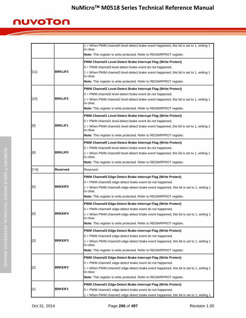
NuMicro M0518 Series Technical Reference Manual
Oct 31, 2014 Page 266 of 497 Revision 1.00
NU
MIC
RO
™ M
0518
SE
RIE
S T
EC
HN
ICA
L R
EF
ER
EN
CE
MA
NU
AL
1 = When PWM channel4 level-detect brake event happened, this bit is set to 1, writing 1 to clear.
Note: This register is write protected. Refer to REGWRPROT register.
[11] BRKLIF3
PWM Channel3 Level-Detect Brake Interrupt Flag (Write Protect)
0 = PWM channel3 level-detect brake event do not happened.
1 = When PWM channel3 level-detect brake event happened, this bit is set to 1, writing 1 to clear.
Note: This register is write protected. Refer to REGWRPROT register.
[10] BRKLIF2
PWM Channel2 Level-Detect Brake Interrupt Flag (Write Protect)
0 = PWM channel2 level-detect brake event do not happened.
1 = When PWM channel2 level-detect brake event happened, this bit is set to 1, writing 1 to clear.
Note: This register is write protected. Refer to REGWRPROT register.
[9] BRKLIF1
PWM Channel1 Level-Detect Brake Interrupt Flag (Write Protect)
0 = PWM channel1 level-detect brake event do not happened.
1 = When PWM channel1 level-detect brake event happened, this bit is set to 1, writing 1 to clear.
Note: This register is write protected. Refer to REGWRPROT register.
[8] BRKLIF0
PWM Channel0 Level-Detect Brake Interrupt Flag (Write Protect)
0 = PWM channel0 level-detect brake event do not happened.
1 = When PWM channel0 level-detect brake event happened, this bit is set to 1, writing 1 to clear.
Note: This register is write protected. Refer to REGWRPROT register.
[7:6] Reserved Reserved.
[5] BRKEIF5
PWM Channel5 Edge-Detect Brake Interrupt Flag (Write Protect)
0 = PWM channel5 edge-detect brake event do not happened.
1 = When PWM channel5 edge-detect brake event happened, this bit is set to 1, writing 1 to clear.
Note: This register is write protected. Refer to REGWRPROT register.
[4] BRKEIF4
PWM Channel4 Edge-Detect Brake Interrupt Flag (Write Protect)
0 = PWM channel4 edge-detect brake event do not happened.
1 = When PWM channel4 edge-detect brake event happened, this bit is set to 1, writing 1 to clear.
Note: This register is write protected. Refer to REGWRPROT register.
[3] BRKEIF3
PWM Channel3 Edge-Detect Brake Interrupt Flag (Write Protect)
0 = PWM channel3 edge-detect brake event do not happened.
1 = When PWM channel3 edge-detect brake event happened, this bit is set to 1, writing 1 to clear.
Note: This register is write protected. Refer to REGWRPROT register.
[2] BRKEIF2
PWM Channel2 Edge-Detect Brake Interrupt Flag (Write Protect)
0 = PWM channel2 edge-detect brake event do not happened.
1 = When PWM channel2 edge-detect brake event happened, this bit is set to 1, writing 1 to clear.
Note: This register is write protected. Refer to REGWRPROT register.
[1] BRKEIF1
PWM Channel1 Edge-Detect Brake Interrupt Flag (Write Protect)
0 = PWM channel1 edge-detect brake event do not happened.
1 = When PWM channel1 edge-detect brake event happened, this bit is set to 1, writing 1
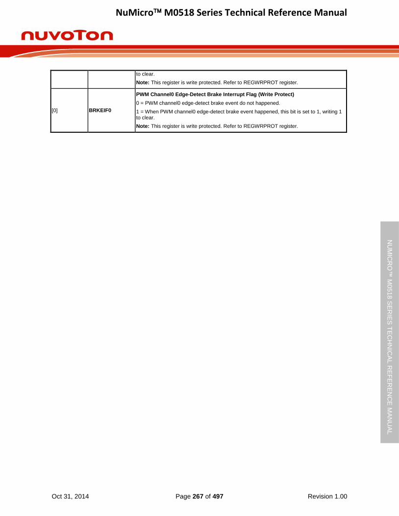
NuMicro M0518 Series Technical Reference Manual
Oct 31, 2014 Page 267 of 497 Revision 1.00
NU
MIC
RO
™ M
0518
SE
RIE
S T
EC
HN
ICA
L R
EF
ER
EN
CE
MA
NU
AL
to clear.
Note: This register is write protected. Refer to REGWRPROT register.
[0] BRKEIF0
PWM Channel0 Edge-Detect Brake Interrupt Flag (Write Protect)
0 = PWM channel0 edge-detect brake event do not happened.
1 = When PWM channel0 edge-detect brake event happened, this bit is set to 1, writing 1 to clear.
Note: This register is write protected. Refer to REGWRPROT register.
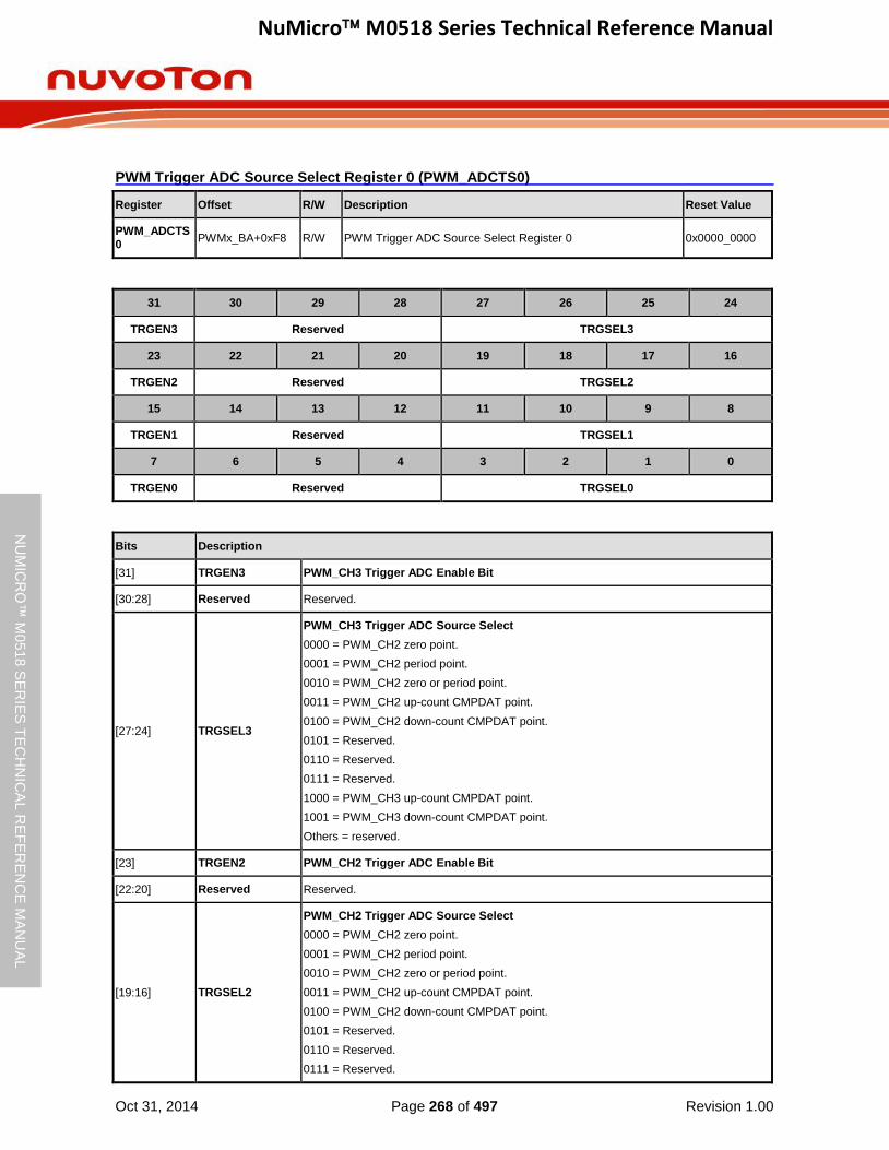
NuMicro M0518 Series Technical Reference Manual
Oct 31, 2014 Page 268 of 497 Revision 1.00
NU
MIC
RO
™ M
0518
SE
RIE
S T
EC
HN
ICA
L R
EF
ER
EN
CE
MA
NU
AL
PWM Trigger ADC Source Select Register 0 (PWM_ADCTS0)
Register Offset R/W Description Reset Value
PWM_ADCTS0
PWMx_BA+0xF8 R/W PWM Trigger ADC Source Select Register 0 0x0000_0000
31 30 29 28 27 26 25 24
TRGEN3 Reserved TRGSEL3
23 22 21 20 19 18 17 16
TRGEN2 Reserved TRGSEL2
15 14 13 12 11 10 9 8
TRGEN1 Reserved TRGSEL1
7 6 5 4 3 2 1 0
TRGEN0 Reserved TRGSEL0
Bits Description
[31] TRGEN3 PWM_CH3 Trigger ADC Enable Bit
[30:28] Reserved Reserved.
[27:24] TRGSEL3
PWM_CH3 Trigger ADC Source Select
0000 = PWM_CH2 zero point.
0001 = PWM_CH2 period point.
0010 = PWM_CH2 zero or period point.
0011 = PWM_CH2 up-count CMPDAT point.
0100 = PWM_CH2 down-count CMPDAT point.
0101 = Reserved.
0110 = Reserved.
0111 = Reserved.
1000 = PWM_CH3 up-count CMPDAT point.
1001 = PWM_CH3 down-count CMPDAT point.
Others = reserved.
[23] TRGEN2 PWM_CH2 Trigger ADC Enable Bit
[22:20] Reserved Reserved.
[19:16] TRGSEL2
PWM_CH2 Trigger ADC Source Select
0000 = PWM_CH2 zero point.
0001 = PWM_CH2 period point.
0010 = PWM_CH2 zero or period point.
0011 = PWM_CH2 up-count CMPDAT point.
0100 = PWM_CH2 down-count CMPDAT point.
0101 = Reserved.
0110 = Reserved.
0111 = Reserved.
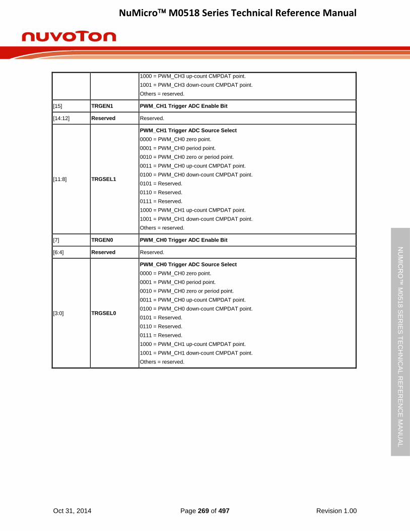
NuMicro M0518 Series Technical Reference Manual
Oct 31, 2014 Page 269 of 497 Revision 1.00
NU
MIC
RO
™ M
0518
SE
RIE
S T
EC
HN
ICA
L R
EF
ER
EN
CE
MA
NU
AL
1000 = PWM_CH3 up-count CMPDAT point.
1001 = PWM_CH3 down-count CMPDAT point.
Others = reserved.
[15] TRGEN1 PWM_CH1 Trigger ADC Enable Bit
[14:12] Reserved Reserved.
[11:8] TRGSEL1
PWM_CH1 Trigger ADC Source Select
0000 = PWM_CH0 zero point.
0001 = PWM_CH0 period point.
0010 = PWM_CH0 zero or period point.
0011 = PWM_CH0 up-count CMPDAT point.
0100 = PWM_CH0 down-count CMPDAT point.
0101 = Reserved.
0110 = Reserved.
0111 = Reserved.
1000 = PWM_CH1 up-count CMPDAT point.
1001 = PWM_CH1 down-count CMPDAT point.
Others = reserved.
[7] TRGEN0 PWM_CH0 Trigger ADC Enable Bit
[6:4] Reserved Reserved.
[3:0] TRGSEL0
PWM_CH0 Trigger ADC Source Select
0000 = PWM_CH0 zero point.
0001 = PWM_CH0 period point.
0010 = PWM_CH0 zero or period point.
0011 = PWM_CH0 up-count CMPDAT point.
0100 = PWM_CH0 down-count CMPDAT point.
0101 = Reserved.
0110 = Reserved.
0111 = Reserved.
1000 = PWM_CH1 up-count CMPDAT point.
1001 = PWM_CH1 down-count CMPDAT point.
Others = reserved.
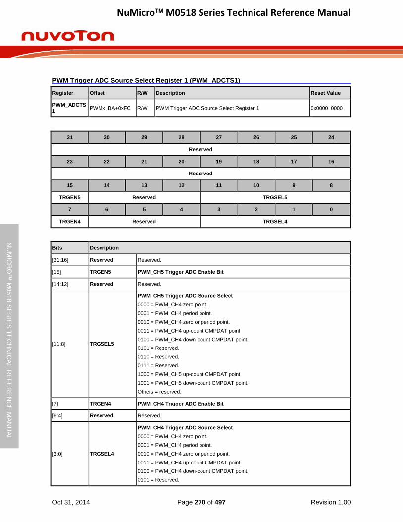
NuMicro M0518 Series Technical Reference Manual
Oct 31, 2014 Page 270 of 497 Revision 1.00
NU
MIC
RO
™ M
0518
SE
RIE
S T
EC
HN
ICA
L R
EF
ER
EN
CE
MA
NU
AL
PWM Trigger ADC Source Select Register 1 (PWM_ADCTS1)
Register Offset R/W Description Reset Value
PWM_ADCTS1
PWMx_BA+0xFC R/W PWM Trigger ADC Source Select Register 1 0x0000_0000
31 30 29 28 27 26 25 24
Reserved
23 22 21 20 19 18 17 16
Reserved
15 14 13 12 11 10 9 8
TRGEN5 Reserved TRGSEL5
7 6 5 4 3 2 1 0
TRGEN4 Reserved TRGSEL4
Bits Description
[31:16] Reserved Reserved.
[15] TRGEN5 PWM_CH5 Trigger ADC Enable Bit
[14:12] Reserved Reserved.
[11:8] TRGSEL5
PWM_CH5 Trigger ADC Source Select
0000 = PWM_CH4 zero point.
0001 = PWM_CH4 period point.
0010 = PWM_CH4 zero or period point.
0011 = PWM_CH4 up-count CMPDAT point.
0100 = PWM_CH4 down-count CMPDAT point.
0101 = Reserved.
0110 = Reserved.
0111 = Reserved.
1000 = PWM_CH5 up-count CMPDAT point.
1001 = PWM_CH5 down-count CMPDAT point.
Others = reserved.
[7] TRGEN4 PWM_CH4 Trigger ADC Enable Bit
[6:4] Reserved Reserved.
[3:0] TRGSEL4
PWM_CH4 Trigger ADC Source Select
0000 = PWM_CH4 zero point.
0001 = PWM_CH4 period point.
0010 = PWM_CH4 zero or period point.
0011 = PWM_CH4 up-count CMPDAT point.
0100 = PWM_CH4 down-count CMPDAT point.
0101 = Reserved.
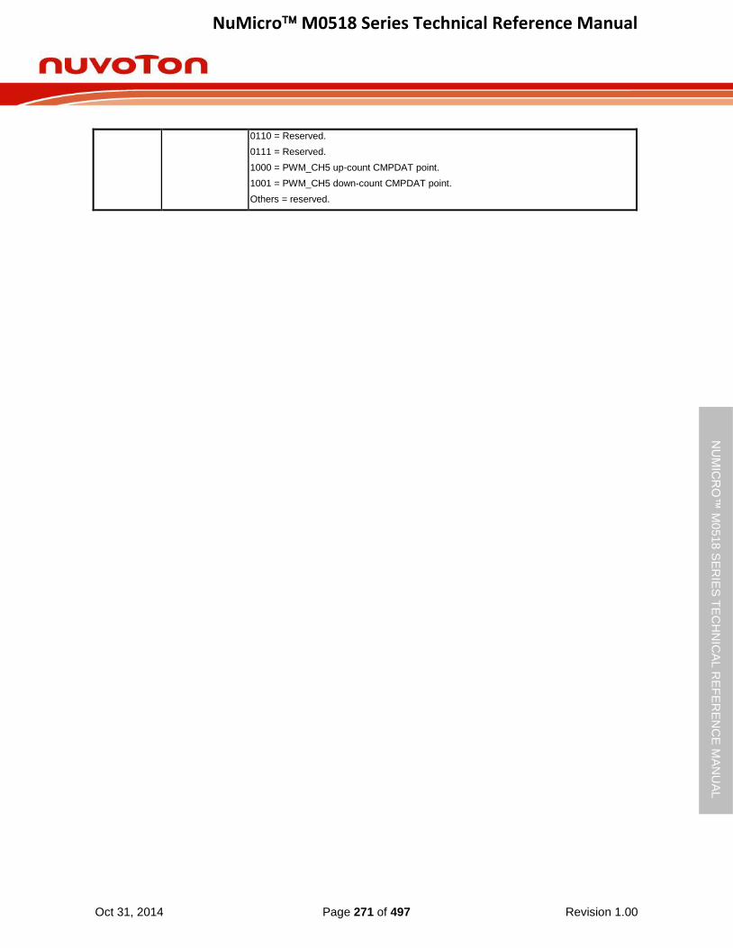
NuMicro M0518 Series Technical Reference Manual
Oct 31, 2014 Page 271 of 497 Revision 1.00
NU
MIC
RO
™ M
0518
SE
RIE
S T
EC
HN
ICA
L R
EF
ER
EN
CE
MA
NU
AL
0110 = Reserved.
0111 = Reserved.
1000 = PWM_CH5 up-count CMPDAT point.
1001 = PWM_CH5 down-count CMPDAT point.
Others = reserved.
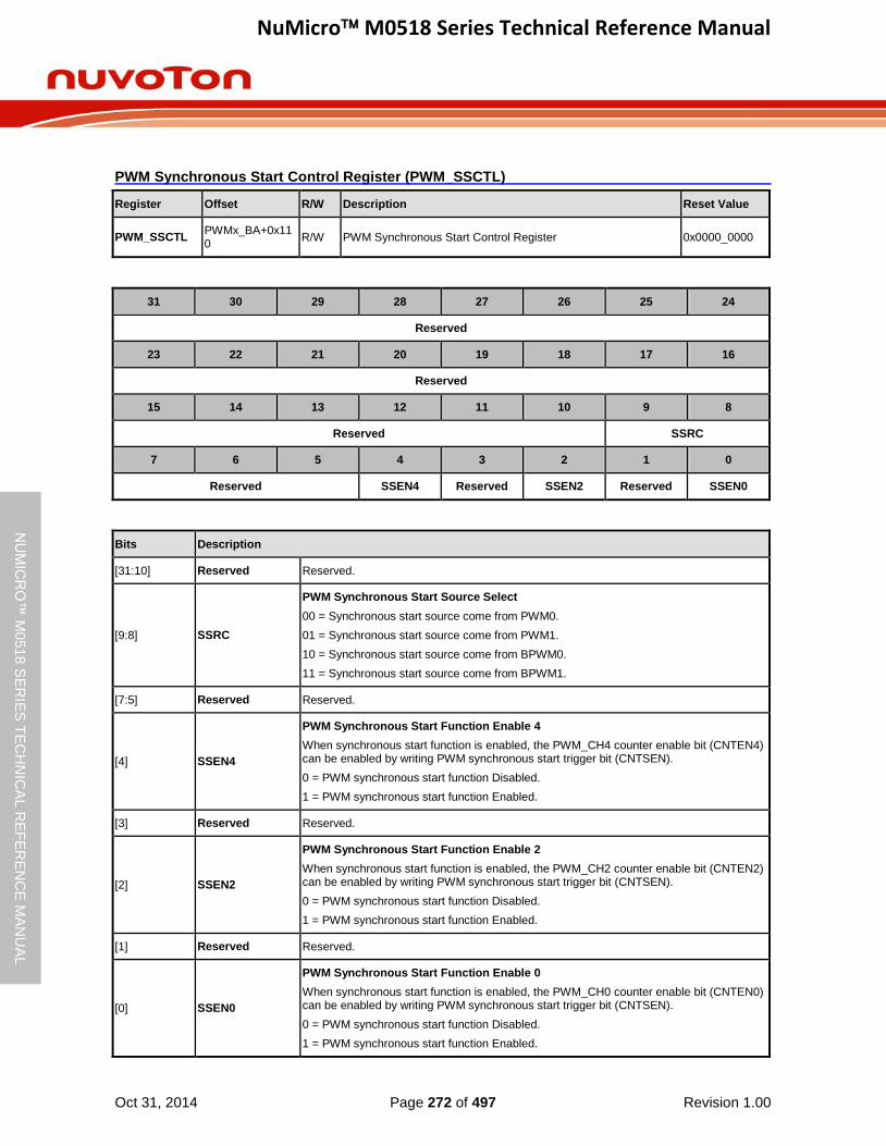
NuMicro M0518 Series Technical Reference Manual
Oct 31, 2014 Page 272 of 497 Revision 1.00
NU
MIC
RO
™ M
0518
SE
RIE
S T
EC
HN
ICA
L R
EF
ER
EN
CE
MA
NU
AL
PWM Synchronous Start Control Register (PWM_SSCTL)
Register Offset R/W Description Reset Value
PWM_SSCTL PWMx_BA+0x110
R/W PWM Synchronous Start Control Register 0x0000_0000
31 30 29 28 27 26 25 24
Reserved
23 22 21 20 19 18 17 16
Reserved
15 14 13 12 11 10 9 8
Reserved SSRC
7 6 5 4 3 2 1 0
Reserved SSEN4 Reserved SSEN2 Reserved SSEN0
Bits Description
[31:10] Reserved Reserved.
[9:8] SSRC
PWM Synchronous Start Source Select
00 = Synchronous start source come from PWM0.
01 = Synchronous start source come from PWM1.
10 = Synchronous start source come from BPWM0.
11 = Synchronous start source come from BPWM1.
[7:5] Reserved Reserved.
[4] SSEN4
PWM Synchronous Start Function Enable 4
When synchronous start function is enabled, the PWM_CH4 counter enable bit (CNTEN4) can be enabled by writing PWM synchronous start trigger bit (CNTSEN).
0 = PWM synchronous start function Disabled.
1 = PWM synchronous start function Enabled.
[3] Reserved Reserved.
[2] SSEN2
PWM Synchronous Start Function Enable 2
When synchronous start function is enabled, the PWM_CH2 counter enable bit (CNTEN2) can be enabled by writing PWM synchronous start trigger bit (CNTSEN).
0 = PWM synchronous start function Disabled.
1 = PWM synchronous start function Enabled.
[1] Reserved Reserved.
[0] SSEN0
PWM Synchronous Start Function Enable 0
When synchronous start function is enabled, the PWM_CH0 counter enable bit (CNTEN0) can be enabled by writing PWM synchronous start trigger bit (CNTSEN).
0 = PWM synchronous start function Disabled.
1 = PWM synchronous start function Enabled.

NuMicro M0518 Series Technical Reference Manual
Oct 31, 2014 Page 273 of 497 Revision 1.00
NU
MIC
RO
™ M
0518
SE
RIE
S T
EC
HN
ICA
L R
EF
ER
EN
CE
MA
NU
AL
PWM Synchronous Start Trigger Register (PWM_SSTRG)
Register Offset R/W Description Reset Value
PWM_SSTRG PWMx_BA+0x114
W PWM Synchronous Start Trigger Register 0x0000_0000
31 30 29 28 27 26 25 24
Reserved
23 22 21 20 19 18 17 16
Reserved
15 14 13 12 11 10 9 8
Reserved
7 6 5 4 3 2 1 0
Reserved CNTSEN
Bits Description
[31:1] Reserved Reserved.
[0] CNTSEN
PWM Counter Synchronous Start Enable (Write Only)
PMW counter synchronous enable function is used to make selected PWM channels (include PWM0_CHx and PWM1_CHx) start counting at the same time.
Writing this bit to 1 will also set the counter enable bit (CNTENn, n denotes channel 0 to 5) if correlated PWM channel counter synchronous start function is enabled.
Note: This bit only present in PWM0_BA.
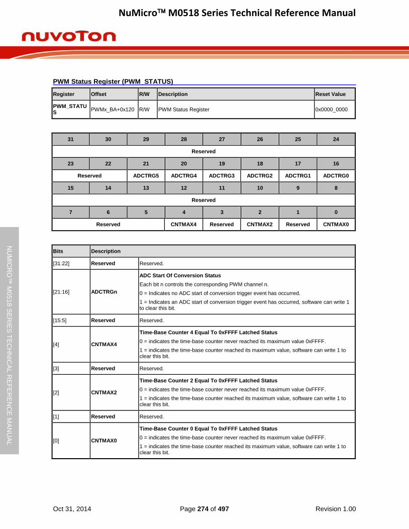
NuMicro M0518 Series Technical Reference Manual
Oct 31, 2014 Page 274 of 497 Revision 1.00
NU
MIC
RO
™ M
0518
SE
RIE
S T
EC
HN
ICA
L R
EF
ER
EN
CE
MA
NU
AL
PWM Status Register (PWM_STATUS)
Register Offset R/W Description Reset Value
PWM_STATUS
PWMx_BA+0x120 R/W PWM Status Register 0x0000_0000
31 30 29 28 27 26 25 24
Reserved
23 22 21 20 19 18 17 16
Reserved ADCTRG5 ADCTRG4 ADCTRG3 ADCTRG2 ADCTRG1 ADCTRG0
15 14 13 12 11 10 9 8
Reserved
7 6 5 4 3 2 1 0
Reserved CNTMAX4 Reserved CNTMAX2 Reserved CNTMAX0
Bits Description
[31:22] Reserved Reserved.
[21:16] ADCTRGn
ADC Start Of Conversion Status
Each bit n controls the corresponding PWM channel n.
0 = Indicates no ADC start of conversion trigger event has occurred.
1 = Indicates an ADC start of conversion trigger event has occurred, software can write 1 to clear this bit.
[15:5] Reserved Reserved.
[4] CNTMAX4
Time-Base Counter 4 Equal To 0xFFFF Latched Status
0 = indicates the time-base counter never reached its maximum value 0xFFFF.
1 = indicates the time-base counter reached its maximum value, software can write 1 to clear this bit.
[3] Reserved Reserved.
[2] CNTMAX2
Time-Base Counter 2 Equal To 0xFFFF Latched Status
0 = indicates the time-base counter never reached its maximum value 0xFFFF.
1 = indicates the time-base counter reached its maximum value, software can write 1 to clear this bit.
[1] Reserved Reserved.
[0] CNTMAX0
Time-Base Counter 0 Equal To 0xFFFF Latched Status
0 = indicates the time-base counter never reached its maximum value 0xFFFF.
1 = indicates the time-base counter reached its maximum value, software can write 1 to clear this bit.

NuMicro M0518 Series Technical Reference Manual
Oct 31, 2014 Page 275 of 497 Revision 1.00
NU
MIC
RO
™ M
0518
SE
RIE
S T
EC
HN
ICA
L R
EF
ER
EN
CE
MA
NU
AL
PWM Capture Input Enable Register (PWM_CAPINEN)
Register Offset R/W Description Reset Value
PWM_CAPINEN
PWMx_BA+0x200 R/W PWM Capture Input Enable Register 0x0000_0000
31 30 29 28 27 26 25 24
Reserved
23 22 21 20 19 18 17 16
Reserved
15 14 13 12 11 10 9 8
Reserved
7 6 5 4 3 2 1 0
Reserved CAPINEN5 CAPINEN4 CAPINEN3 CAPINEN2 CAPINEN1 CAPINEN0
Bits Description
[31:6] Reserved Reserved.
[5:0] CAPINENn
Capture Input Enable Control
Each bit n controls the corresponding PWM channel n.
0 = PWM Channel capture input path Disabled. The input of PWM channel capture function is always regarded as 0.
1 = PWM Channel capture input path Enabled. The input of PWM channel capture function comes from correlative multifunction pin.

NuMicro M0518 Series Technical Reference Manual
Oct 31, 2014 Page 276 of 497 Revision 1.00
NU
MIC
RO
™ M
0518
SE
RIE
S T
EC
HN
ICA
L R
EF
ER
EN
CE
MA
NU
AL
PWM Capture Control Register (PWM_CAPCTL)
Register Offset R/W Description Reset Value
PWM_CAPCTL
PWMx_BA+0x204 R/W PWM Capture Control Register 0x0000_0000
31 30 29 28 27 26 25 24
Reserved FCRLDEN5 FCRLDEN4 FCRLDEN3 FCRLDEN2 FCRLDEN1 FCRLDEN0
23 22 21 20 19 18 17 16
Reserved RCRLDEN5 RCRLDEN4 RCRLDEN3 RCRLDEN2 RCRLDEN1 RCRLDEN0
15 14 13 12 11 10 9 8
Reserved CAPINV5 CAPINV4 CAPINV3 CAPINV2 CAPINV1 CAPINV0
7 6 5 4 3 2 1 0
Reserved CAPEN5 CAPEN4 CAPEN3 CAPEN2 CAPEN1 CAPEN0
Bits Description
[31:30] Reserved Reserved.
[29:24] FCRLDENn
Falling Capture Reload Enable Control
Each bit n controls the corresponding PWM channel n.
0 = Falling capture reload counter Disabled.
1 = Falling capture reload counter Enabled.
[23:22] Reserved Reserved.
[21:16] RCRLDENn
Rising Capture Reload Enable Control
Each bit n controls the corresponding PWM channel n.
0 = Rising capture reload counter Disabled.
1 = Rising capture reload counter Enabled.
[15:14] Reserved Reserved.
[13:8] CAPINVn
Capture Inverter Enable Control
Each bit n controls the corresponding PWM channel n.
0 = Capture source inverter Disabled.
1 = Capture source inverter Enabled. Reverse the input signal from GPIO.
[7:6] Reserved Reserved.
[5:0] CAPENn
Capture Function Enable Control
Each bit n controls the corresponding PWM channel n.
0 = Capture function Disabled. RCAPDAT/FCAPDAT register will not be updated.
1 = Capture function Enabled. Capture latched the PWM counter value when detected rising or falling edge of input signal and saved to RCAPDAT (Rising latch) and FCAPDAT (Falling latch).
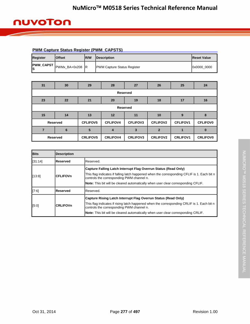
NuMicro M0518 Series Technical Reference Manual
Oct 31, 2014 Page 277 of 497 Revision 1.00
NU
MIC
RO
™ M
0518
SE
RIE
S T
EC
HN
ICA
L R
EF
ER
EN
CE
MA
NU
AL
PWM Capture Status Register (PWM_CAPSTS)
Register Offset R/W Description Reset Value
PWM_CAPSTS
PWMx_BA+0x208 R PWM Capture Status Register 0x0000_0000
31 30 29 28 27 26 25 24
Reserved
23 22 21 20 19 18 17 16
Reserved
15 14 13 12 11 10 9 8
Reserved CFLIFOV5 CFLIFOV4 CFLIFOV3 CFLIFOV2 CFLIFOV1 CFLIFOV0
7 6 5 4 3 2 1 0
Reserved CRLIFOV5 CRLIFOV4 CRLIFOV3 CRLIFOV2 CRLIFOV1 CRLIFOV0
Bits Description
[31:14] Reserved Reserved.
[13:8] CFLIFOVn
Capture Falling Latch Interrupt Flag Overrun Status (Read Only)
This flag indicates if falling latch happened when the corresponding CFLIF is 1. Each bit n controls the corresponding PWM channel n.
Note: This bit will be cleared automatically when user clear corresponding CFLIF.
[7:6] Reserved Reserved.
[5:0] CRLIFOVn
Capture Rising Latch Interrupt Flag Overrun Status (Read Only)
This flag indicates if rising latch happened when the corresponding CRLIF is 1. Each bit n controls the corresponding PWM channel n.
Note: This bit will be cleared automatically when user clear corresponding CRLIF.
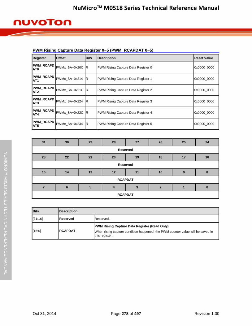
NuMicro M0518 Series Technical Reference Manual
Oct 31, 2014 Page 278 of 497 Revision 1.00
NU
MIC
RO
™ M
0518
SE
RIE
S T
EC
HN
ICA
L R
EF
ER
EN
CE
MA
NU
AL
PWM Rising Capture Data Register 0~5 (PWM_RCAPDAT 0~5)
Register Offset R/W Description Reset Value
PWM_RCAPDAT0
PWMx_BA+0x20C R PWM Rising Capture Data Register 0 0x0000_0000
PWM_RCAPDAT1
PWMx_BA+0x214 R PWM Rising Capture Data Register 1 0x0000_0000
PWM_RCAPDAT2
PWMx_BA+0x21C R PWM Rising Capture Data Register 2 0x0000_0000
PWM_RCAPDAT3
PWMx_BA+0x224 R PWM Rising Capture Data Register 3 0x0000_0000
PWM_RCAPDAT4
PWMx_BA+0x22C R PWM Rising Capture Data Register 4 0x0000_0000
PWM_RCAPDAT5
PWMx_BA+0x234 R PWM Rising Capture Data Register 5 0x0000_0000
31 30 29 28 27 26 25 24
Reserved
23 22 21 20 19 18 17 16
Reserved
15 14 13 12 11 10 9 8
RCAPDAT
7 6 5 4 3 2 1 0
RCAPDAT
Bits Description
[31:16] Reserved Reserved.
[15:0] RCAPDAT
PWM Rising Capture Data Register (Read Only)
When rising capture condition happened, the PWM counter value will be saved in this register.

NuMicro M0518 Series Technical Reference Manual
Oct 31, 2014 Page 279 of 497 Revision 1.00
NU
MIC
RO
™ M
0518
SE
RIE
S T
EC
HN
ICA
L R
EF
ER
EN
CE
MA
NU
AL
PWM Falling Capture Data Register 0~5 (PWM_FCAPDAT 0~5)
Register Offset R/W Description Reset Value
PWM_FCAPDAT0
PWMx_BA+0x210 R PWM Falling Capture Data Register 0 0x0000_0000
PWM_FCAPDAT1
PWMx_BA+0x218 R PWM Falling Capture Data Register 1 0x0000_0000
PWM_FCAPDAT2
PWMx_BA+0x220 R PWM Falling Capture Data Register 2 0x0000_0000
PWM_FCAPDAT3
PWMx_BA+0x228 R PWM Falling Capture Data Register 3 0x0000_0000
PWM_FCAPDAT4
PWMx_BA+0x230 R PWM Falling Capture Data Register 4 0x0000_0000
PWM_FCAPDAT5
PWMx_BA+0x238 R PWM Falling Capture Data Register 5 0x0000_0000
31 30 29 28 27 26 25 24
Reserved
23 22 21 20 19 18 17 16
Reserved
15 14 13 12 11 10 9 8
FCAPDAT
7 6 5 4 3 2 1 0
FCAPDAT
Bits Description
[31:16] Reserved Reserved.
[15:0] FCAPDAT
PWM Falling Capture Data Register (Read Only)
When falling capture condition happened, the PWM counter value will be saved in this register.

NuMicro M0518 Series Technical Reference Manual
Oct 31, 2014 Page 280 of 497 Revision 1.00
NU
MIC
RO
™ M
0518
SE
RIE
S T
EC
HN
ICA
L R
EF
ER
EN
CE
MA
NU
AL
PWM Capture Interrupt Enable Register (PWM_CAPIEN)
Register Offset R/W Description Reset Value
PWM_CAPIEN
PWMx_BA+0x250 R/W PWM Capture Interrupt Enable Register 0x0000_0000
31 30 29 28 27 26 25 24
Reserved
23 22 21 20 19 18 17 16
Reserved
15 14 13 12 11 10 9 8
Reserved CAPFIEN5 CAPFIEN4 CAPFIEN3 CAPFIEN2 CAPFIEN1 CAPFIEN0
7 6 5 4 3 2 1 0
Reserved CAPRIEN5 CAPRIEN4 CAPRIEN3 CAPRIEN2 CAPRIEN1 CAPRIEN0
Bits Description
[31:14] Reserved Reserved.
[13:8] CAPFIENn
PWM Capture Falling Latch Interrupt Enable Control
Each bit n controls the corresponding PWM channel n.
0 = Capture falling edge latch interrupt Disabled.
1 = Capture falling edge latch interrupt Enabled.
[7:6] Reserved Reserved.
[5:0] CAPRIENn
PWM Capture Rising Latch Interrupt Enable Control
Each bit n controls the corresponding PWM channel n.
0 = Capture rising edge latch interrupt Disabled.
1 = Capture rising edge latch interrupt Enabled.
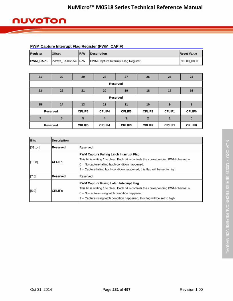
NuMicro M0518 Series Technical Reference Manual
Oct 31, 2014 Page 281 of 497 Revision 1.00
NU
MIC
RO
™ M
0518
SE
RIE
S T
EC
HN
ICA
L R
EF
ER
EN
CE
MA
NU
AL
PWM Capture Interrupt Flag Register (PWM_CAPIF)
Register Offset R/W Description Reset Value
PWM_CAPIF PWMx_BA+0x254 R/W PWM Capture Interrupt Flag Register 0x0000_0000
31 30 29 28 27 26 25 24
Reserved
23 22 21 20 19 18 17 16
Reserved
15 14 13 12 11 10 9 8
Reserved CFLIF5 CFLIF4 CFLIF3 CFLIF2 CFLIF1 CFLIF0
7 6 5 4 3 2 1 0
Reserved CRLIF5 CRLIF4 CRLIF3 CRLIF2 CRLIF1 CRLIF0
Bits Description
[31:14] Reserved Reserved.
[13:8] CFLIFn
PWM Capture Falling Latch Interrupt Flag
This bit is writing 1 to clear. Each bit n controls the corresponding PWM channel n.
0 = No capture falling latch condition happened.
1 = Capture falling latch condition happened, this flag will be set to high.
[7:6] Reserved Reserved.
[5:0] CRLIFn
PWM Capture Rising Latch Interrupt Flag
This bit is writing 1 to clear. Each bit n controls the corresponding PWM channel n.
0 = No capture rising latch condition happened.
1 = Capture rising latch condition happened, this flag will be set to high.
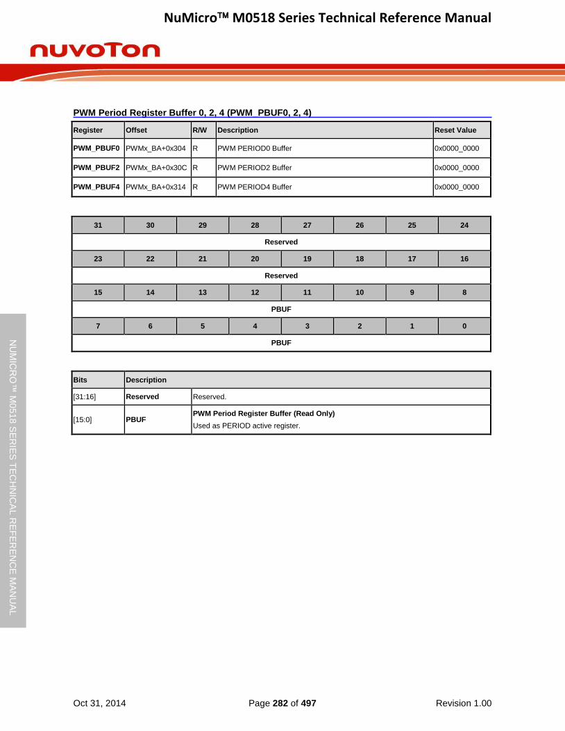
NuMicro M0518 Series Technical Reference Manual
Oct 31, 2014 Page 282 of 497 Revision 1.00
NU
MIC
RO
™ M
0518
SE
RIE
S T
EC
HN
ICA
L R
EF
ER
EN
CE
MA
NU
AL
PWM Period Register Buffer 0, 2, 4 (PWM_PBUF0, 2, 4)
Register Offset R/W Description Reset Value
PWM_PBUF0 PWMx_BA+0x304 R PWM PERIOD0 Buffer 0x0000_0000
PWM_PBUF2 PWMx_BA+0x30C R PWM PERIOD2 Buffer 0x0000_0000
PWM_PBUF4 PWMx_BA+0x314 R PWM PERIOD4 Buffer 0x0000_0000
31 30 29 28 27 26 25 24
Reserved
23 22 21 20 19 18 17 16
Reserved
15 14 13 12 11 10 9 8
PBUF
7 6 5 4 3 2 1 0
PBUF
Bits Description
[31:16] Reserved Reserved.
[15:0] PBUF PWM Period Register Buffer (Read Only)
Used as PERIOD active register.
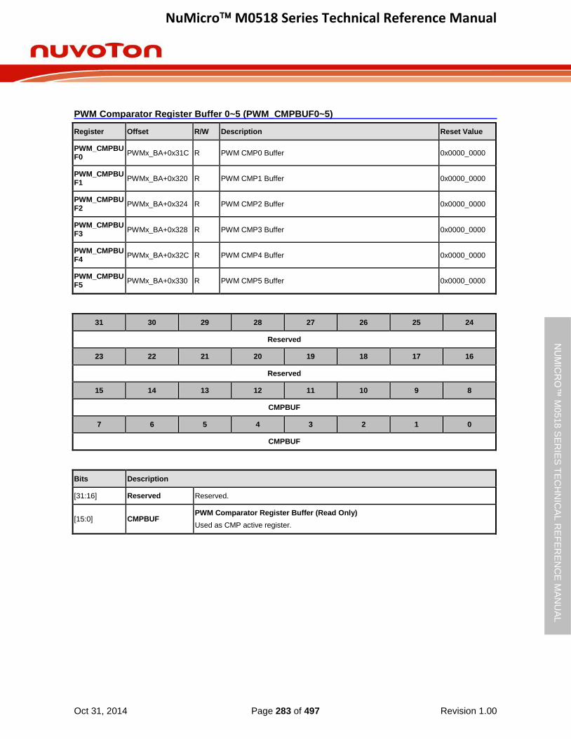
NuMicro M0518 Series Technical Reference Manual
Oct 31, 2014 Page 283 of 497 Revision 1.00
NU
MIC
RO
™ M
0518
SE
RIE
S T
EC
HN
ICA
L R
EF
ER
EN
CE
MA
NU
AL
PWM Comparator Register Buffer 0~5 (PWM_CMPBUF0~5)
Register Offset R/W Description Reset Value
PWM_CMPBUF0
PWMx_BA+0x31C R PWM CMP0 Buffer 0x0000_0000
PWM_CMPBUF1
PWMx_BA+0x320 R PWM CMP1 Buffer 0x0000_0000
PWM_CMPBUF2
PWMx_BA+0x324 R PWM CMP2 Buffer 0x0000_0000
PWM_CMPBUF3
PWMx_BA+0x328 R PWM CMP3 Buffer 0x0000_0000
PWM_CMPBUF4
PWMx_BA+0x32C R PWM CMP4 Buffer 0x0000_0000
PWM_CMPBUF5
PWMx_BA+0x330 R PWM CMP5 Buffer 0x0000_0000
31 30 29 28 27 26 25 24
Reserved
23 22 21 20 19 18 17 16
Reserved
15 14 13 12 11 10 9 8
CMPBUF
7 6 5 4 3 2 1 0
CMPBUF
Bits Description
[31:16] Reserved Reserved.
[15:0] CMPBUF PWM Comparator Register Buffer (Read Only)
Used as CMP active register.
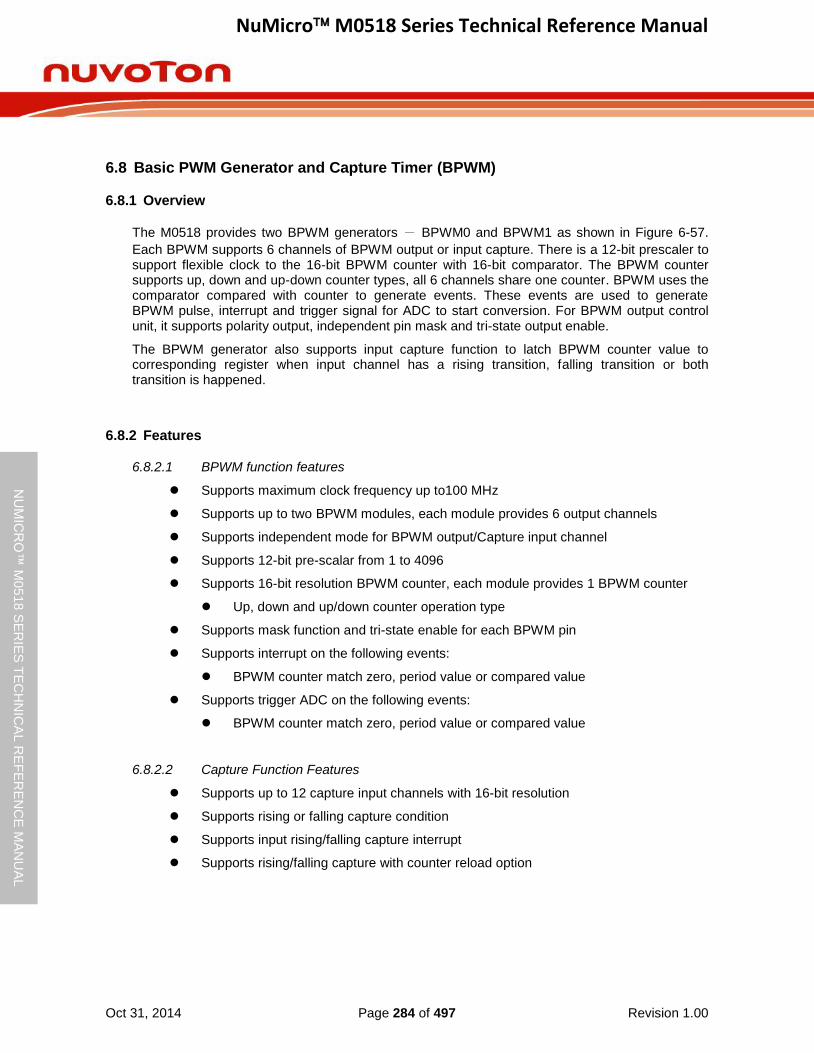
NuMicro M0518 Series Technical Reference Manual
Oct 31, 2014 Page 284 of 497 Revision 1.00
NU
MIC
RO
™ M
0518
SE
RIE
S T
EC
HN
ICA
L R
EF
ER
EN
CE
MA
NU
AL
6.8 Basic PWM Generator and Capture Timer (BPWM)
6.8.1 Overview
The M0518 provides two BPWM generators - BPWM0 and BPWM1 as shown in Figure 6-57.
Each BPWM supports 6 channels of BPWM output or input capture. There is a 12-bit prescaler to support flexible clock to the 16-bit BPWM counter with 16-bit comparator. The BPWM counter supports up, down and up-down counter types, all 6 channels share one counter. BPWM uses the comparator compared with counter to generate events. These events are used to generate BPWM pulse, interrupt and trigger signal for ADC to start conversion. For BPWM output control unit, it supports polarity output, independent pin mask and tri-state output enable.
The BPWM generator also supports input capture function to latch BPWM counter value to corresponding register when input channel has a rising transition, falling transition or both transition is happened.
6.8.2 Features
6.8.2.1 BPWM function features
Supports maximum clock frequency up to100 MHz
Supports up to two BPWM modules, each module provides 6 output channels
Supports independent mode for BPWM output/Capture input channel
Supports 12-bit pre-scalar from 1 to 4096
Supports 16-bit resolution BPWM counter, each module provides 1 BPWM counter
Up, down and up/down counter operation type
Supports mask function and tri-state enable for each BPWM pin
Supports interrupt on the following events:
BPWM counter match zero, period value or compared value
Supports trigger ADC on the following events:
BPWM counter match zero, period value or compared value
6.8.2.2 Capture Function Features
Supports up to 12 capture input channels with 16-bit resolution
Supports rising or falling capture condition
Supports input rising/falling capture interrupt
Supports rising/falling capture with counter reload option
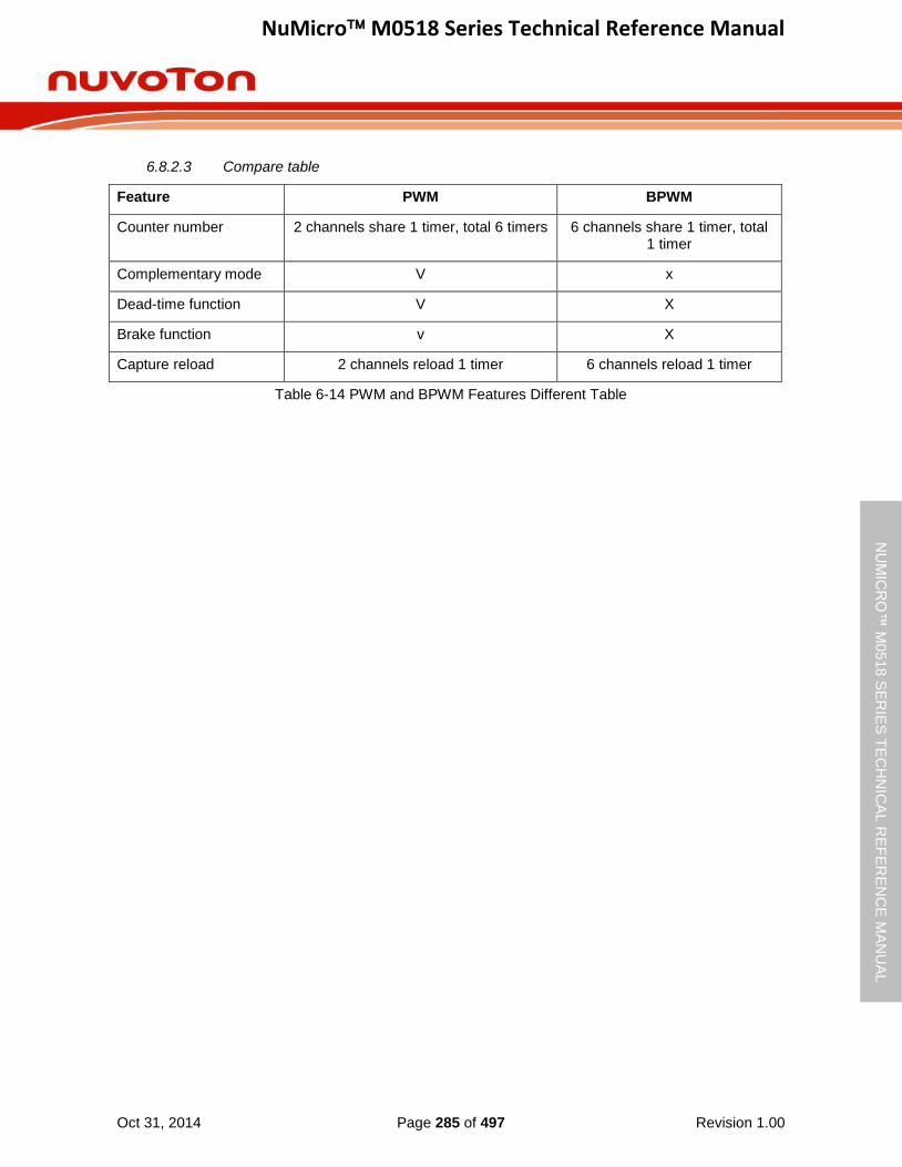
NuMicro M0518 Series Technical Reference Manual
Oct 31, 2014 Page 285 of 497 Revision 1.00
NU
MIC
RO
™ M
0518
SE
RIE
S T
EC
HN
ICA
L R
EF
ER
EN
CE
MA
NU
AL
6.8.2.3 Compare table
Feature PWM BPWM
Counter number 2 channels share 1 timer, total 6 timers 6 channels share 1 timer, total 1 timer
Complementary mode V x
Dead-time function V X
Brake function v X
Capture reload 2 channels reload 1 timer 6 channels reload 1 timer
Table 6-14 PWM and BPWM Features Different Table

NuMicro M0518 Series Technical Reference Manual
Oct 31, 2014 Page 286 of 497 Revision 1.00
NU
MIC
RO
™ M
0518
SE
RIE
S T
EC
HN
ICA
L R
EF
ER
EN
CE
MA
NU
AL
6.8.3 Block Diagram
AP
B
BPWM0
SYNC_IN
TIMER0
ADC
CLOCK
CONTROLLER 5
BPWM1
TIMER1
TIMER2
TIMER3
BPWM0_CH0
BPWM0_CH5
4
4 NVIC_MUX
6
6
BPWM1_CH5
BPWM1_CH0
Figure 6-57 BPWM Generator Overview Block Diagram
PWM system clock frequency can be set equal or double to HCLK frequency as Figure 6-58, the detail register setting, please refer to Table 6-15.
Each PWM generator has only one clock source input and can be selected from system clock or four TIMER trigger PWM outputs as Figure 6-59 by ECLKSRC0 (BPWM_CLKSRC[2:0]) for BPWM_CLK0.
HCLK_S (CLKSEL0[2:0])
1/(HCLK_N+1) HCLK0
1
0
1
BPWM0
system clock
BPWM1
system clock
PCLK
PCLK
BPWM1_S (CLKSEL3[19])
BPWM0_S (CLKSEL3[18])
BPWM0_EN (APBCLK1[18])
BPWM1_EN (APBCLK1[19])
HCLK_N (CLKDIV[3:0])
0
1
2
3
7
4~24MHzReservedPLLFOUT
10kHz22.1184MHz
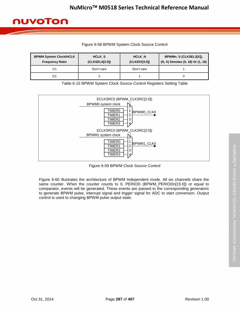
NuMicro M0518 Series Technical Reference Manual
Oct 31, 2014 Page 287 of 497 Revision 1.00
NU
MIC
RO
™ M
0518
SE
RIE
S T
EC
HN
ICA
L R
EF
ER
EN
CE
MA
NU
AL
Figure 6-58 BPWM System Clock Source Control
Table 6-15 BPWM System Clock Source Control Registers Setting Table
BPWM0 system clock
BPWM1 system clock
TIMER0
TIMER1
TIMER2TIMER3
0
1
2
34
TIMER0
TIMER1
TIMER2TIMER3
0
1
2
34
ECLKSRC0 (BPWM_CLKSRC[2:0])
ECLKSRC0 (BPWM_CLKSRC[2:0])
BPWM0_CLK0
BPWM1_CLK0
Figure 6-59 BPWM Clock Source Control
Figure 6-60 illustrates the architecture of BPWM Independent mode. All six channels share the same counter. When the counter counts to 0, PERIOD (BPWM_PERIODn[15:0]) or equal to comparator, events will be generated. These events are passed to the corresponding generators to generate BPWM pulse, interrupt signal and trigger signal for ADC to start conversion. Output control is used to changing BPWM pulse output state.
BPWM System Clock/HCLK
Frequency Ratio
HCLK_S
(CLKSEL0[2:0])
HCLK_N
(CLKDIV[3:0])
BPWMn_S (CLKSEL3[X]),
(N, X) Denotes (0, 18) Or (1, 19)
1/1 Don’t care Don’t care 1
2/1 2 1 0
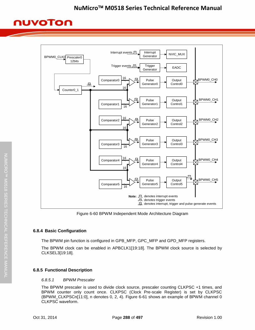
NuMicro M0518 Series Technical Reference Manual
Oct 31, 2014 Page 288 of 497 Revision 1.00
NU
MIC
RO
™ M
0518
SE
RIE
S T
EC
HN
ICA
L R
EF
ER
EN
CE
MA
NU
AL
Prescaler0
12bits
Interrupt
Generator
Trigger
Generator
NVIC_MUX
EADC
BPWM0_CH0Pulse
Generator0
Output
Control0
Pulse
Generator1
Output
Control1
BPWM0_CH1
BPWM0_CH2Pulse
Generator2
Output
Control2
Pulse
Generator3
Output
Control3
BPWM0_CH3
BPWM0_CH4Pulse
Generator4
Output
Control4
Pulse
Generator5
Output
Control5
BPWM0_CH5
BPWM0_CLK0
i
Trigger events
Interrupt events
t
i
16
16
16Comparator1
Comparator0
Counter0_1
a
a
a
16
16
16Comparator3
Comparator2
a
a
16
16
16Comparator5
Comparator4
a
a
a
it
denotes interrupt events
denotes trigger events
denotes interrupt, trigger and pulse generate events
Note:
Figure 6-60 BPWM Independent Mode Architecture Diagram
6.8.4 Basic Configuration
The BPWM pin function is configured in GPB_MFP, GPC_MFP and GPD_MFP registers.
The BPWM clock can be enabled in APBCLK1[19:18]. The BPWM clock source is selected by CLKSEL3[19:18].
6.8.5 Functional Description
6.8.5.1 BPWM Prescaler
The BPWM prescaler is used to divide clock source, prescaler counting CLKPSC +1 times, and BPWM counter only count once. CLKPSC (Clock Pre-scale Register) is set by CLKPSC (BPWM_CLKPSCn[11:0], n denotes 0, 2, 4). Figure 6-61 shows an example of BPWM channel 0 CLKPSC waveform.
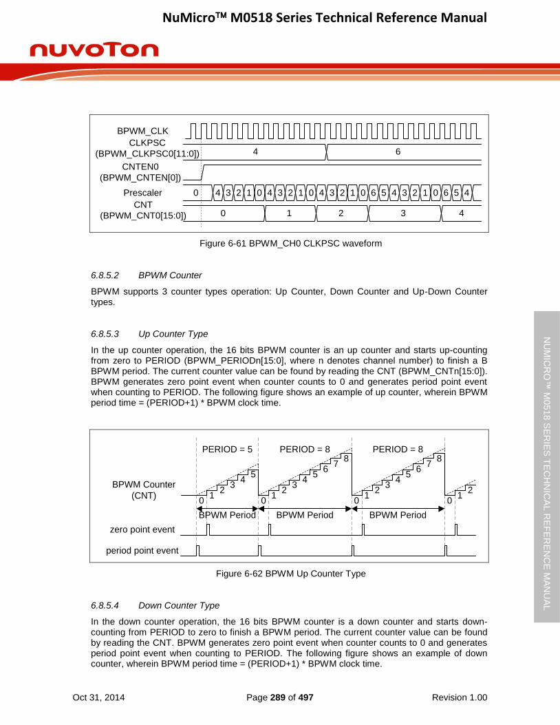
NuMicro M0518 Series Technical Reference Manual
Oct 31, 2014 Page 289 of 497 Revision 1.00
NU
MIC
RO
™ M
0518
SE
RIE
S T
EC
HN
ICA
L R
EF
ER
EN
CE
MA
NU
AL
0 1CNT
(BPWM_CNT0[15:0])
4Prescaler
CLKPSC
(BPWM_CLKPSC0[11:0])
3 2 1 0
3
CNTEN0
(BPWM_CNTEN[0])
4 3 2 1 0 4 3 2 1 0 5 4 3 2 16 00
4 6
2 4
5 46
BPWM_CLK
Figure 6-61 BPWM_CH0 CLKPSC waveform
6.8.5.2 BPWM Counter
BPWM supports 3 counter types operation: Up Counter, Down Counter and Up-Down Counter types.
6.8.5.3 Up Counter Type
In the up counter operation, the 16 bits BPWM counter is an up counter and starts up-counting from zero to PERIOD (BPWM_PERIODn[15:0], where n denotes channel number) to finish a B BPWM period. The current counter value can be found by reading the CNT (BPWM_CNTn[15:0]). BPWM generates zero point event when counter counts to 0 and generates period point event when counting to PERIOD. The following figure shows an example of up counter, wherein BPWM period time = (PERIOD+1) * BPWM clock time.
01
23
45
BPWM Counter
(CNT)0
12
34
56
78
01
23
45
67
8
01
2
BPWM Period BPWM Period
PERIOD = 5 PERIOD = 8
BPWM Period
PERIOD = 8
zero point event
period point event
Figure 6-62 BPWM Up Counter Type
6.8.5.4 Down Counter Type
In the down counter operation, the 16 bits BPWM counter is a down counter and starts down-counting from PERIOD to zero to finish a BPWM period. The current counter value can be found by reading the CNT. BPWM generates zero point event when counter counts to 0 and generates period point event when counting to PERIOD. The following figure shows an example of down counter, wherein BPWM period time = (PERIOD+1) * BPWM clock time.

NuMicro M0518 Series Technical Reference Manual
Oct 31, 2014 Page 290 of 497 Revision 1.00
NU
MIC
RO
™ M
0518
SE
RIE
S T
EC
HN
ICA
L R
EF
ER
EN
CE
MA
NU
AL
01
23
45
01
23
45
67
8
01
23
45
67
86
78
BPWM Counter
(CNT)
BPWM Period BPWM Period BPWM Period
PERIOD = 5 PERIOD = 8 PERIOD = 8
zero point event
period point event
Figure 6-63 BPWM Down Counter Type
6.8.5.5 Up-Down Counter Type
In the up-down counter operation, the 16 bits BPWM counter is an up-down counter and starts counting-up from zero to PERIOD and then starts counting down to zero to finish a BPWM period. The current counter value can be found by reading the CNT. BPWM generates zero point event when counter counts to 0 and generates center point event when counting to PERIOD. The following figure shows an example of up-down counter, wherein BPWM period time = (2xPERIOD) * BPWM clock time. The DIRF (BPWM_CNTn[16]) is counter direction indicator flag, where high is up counting, and low is down counting.
BPWM Direction
(DIRF)
BPWM Counter
(CNT)0
12
34
31
20
12
34
31
20
56
76
45
12
34
BPWM Period
PERIOD = 4 PERIOD = 7
BPWM Period
zero point event
center point event
Figure 6-64 BPWM Up-Down Counter Type
6.8.5.6 BPWM Comparator
The CMPDAT (BPWM_CMPDATn[15:0]) is a basic comparator register of BPWM channel n; each channel only has one CMPDAT. The CMPDAT’s value is continuously compared to the counter value. When the counter is equal to compared register, BPWM generates an event and uses the event to generate BPWM pulse, interrupt or use to trigger ADC. In up-down counter type, two events will be generated in a BPWM period as shown in Figure 6-65.
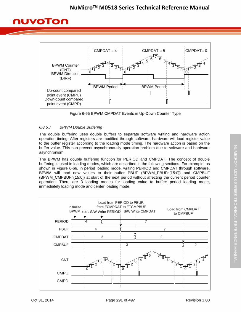
NuMicro M0518 Series Technical Reference Manual
Oct 31, 2014 Page 291 of 497 Revision 1.00
NU
MIC
RO
™ M
0518
SE
RIE
S T
EC
HN
ICA
L R
EF
ER
EN
CE
MA
NU
AL
BPWM Direction
(DIRF)
BPWM Counter
(CNT)0
12
34
31
20
12
34
31
20
56
76
45
12
34
BPWM Period
CMPDAT = 4 CMPDAT = 5
BPWM PeriodUp-count compared
point event (CMPU)Down-count compared
point event (CMPD)
CMPDAT= 0
Figure 6-65 BPWM CMPDAT Events in Up-Down Counter Type
6.8.5.7 BPWM Double Buffering
The double buffering uses double buffers to separate software writing and hardware action operation timing. After registers are modified through software, hardware will load register value to the buffer register according to the loading mode timing. The hardware action is based on the buffer value. This can prevent asynchronously operation problem due to software and hardware asynchronism.
The BPWM has double buffering function for PERIOD and CMPDAT. The concept of double buffering is used in loading modes, which are described in the following sections. For example, as shown in Figure 6-66, in period loading mode, writing PERIOD and CMPDAT through software, BPWM will load new values to their buffer PBUF (BPWM_PBUFn[15:0]) and CMPBUF (BPWM_CMPBUFn[15:0]) at start of the next period without affecting the current period counter operation. There are 3 loading modes for loading value to buffer: period loading mode, immediately loading mode and center loading mode.
CMPDAT
PERIOD
S/W Write PERIOD
CNT
4 7
3
start
Initialize
BPWM
2
S/W Write CMPDAT
01
23
43
12
01
23
43
12
0
56
76
45
12
34
Load from PERIOD to PBUF,
from FCMPDAT to FTCMPBUF Load from CMPDAT
to CMPBUF
PBUF 4 7
CMPBUF 3 2
CMPU
CMPD
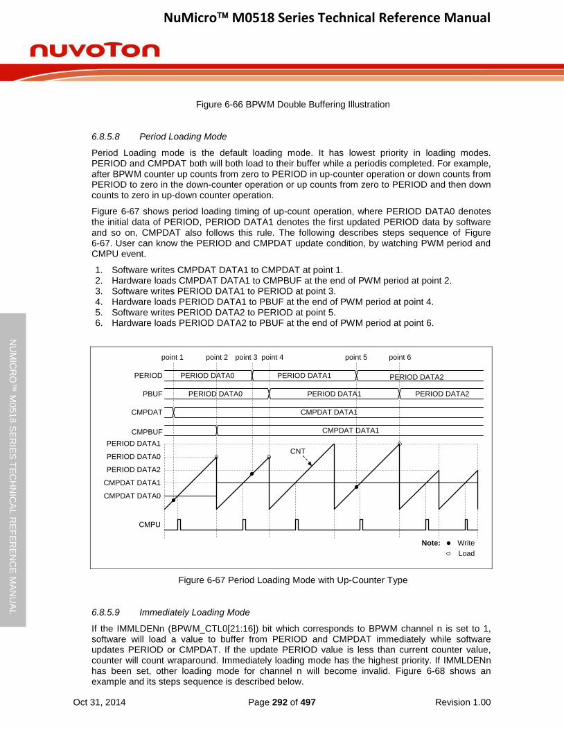
NuMicro M0518 Series Technical Reference Manual
Oct 31, 2014 Page 292 of 497 Revision 1.00
NU
MIC
RO
™ M
0518
SE
RIE
S T
EC
HN
ICA
L R
EF
ER
EN
CE
MA
NU
AL
Figure 6-66 BPWM Double Buffering Illustration
6.8.5.8 Period Loading Mode
Period Loading mode is the default loading mode. It has lowest priority in loading modes. PERIOD and CMPDAT both will both load to their buffer while a periodis completed. For example, after BPWM counter up counts from zero to PERIOD in up-counter operation or down counts from PERIOD to zero in the down-counter operation or up counts from zero to PERIOD and then down counts to zero in up-down counter operation.
Figure 6-67 shows period loading timing of up-count operation, where PERIOD DATA0 denotes the initial data of PERIOD, PERIOD DATA1 denotes the first updated PERIOD data by software and so on, CMPDAT also follows this rule. The following describes steps sequence of Figure 6-67. User can know the PERIOD and CMPDAT update condition, by watching PWM period and CMPU event.
1. Software writes CMPDAT DATA1 to CMPDAT at point 1. 2. Hardware loads CMPDAT DATA1 to CMPBUF at the end of PWM period at point 2. 3. Software writes PERIOD DATA1 to PERIOD at point 3. 4. Hardware loads PERIOD DATA1 to PBUF at the end of PWM period at point 4. 5. Software writes PERIOD DATA2 to PERIOD at point 5. 6. Hardware loads PERIOD DATA2 to PBUF at the end of PWM period at point 6.
CMPDAT DATA0
CMPU
CMPDAT DATA1
PERIOD DATA0
PERIOD DATA1
PERIOD DATA2
CNT
Write
Load
Note:
CMPDAT
PERIOD PERIOD DATA0 PERIOD DATA1
CMPDAT DATA1
PBUF PERIOD DATA0 PERIOD DATA1
CMPBUF CMPDAT DATA1
PERIOD DATA2
PERIOD DATA2
point 1 point 2 point 3 point 4 point 5 point 6
Figure 6-67 Period Loading Mode with Up-Counter Type
6.8.5.9 Immediately Loading Mode
If the IMMLDENn (BPWM_CTL0[21:16]) bit which corresponds to BPWM channel n is set to 1, software will load a value to buffer from PERIOD and CMPDAT immediately while software updates PERIOD or CMPDAT. If the update PERIOD value is less than current counter value, counter will count wraparound. Immediately loading mode has the highest priority. If IMMLDENn has been set, other loading mode for channel n will become invalid. Figure 6-68 shows an example and its steps sequence is described below.
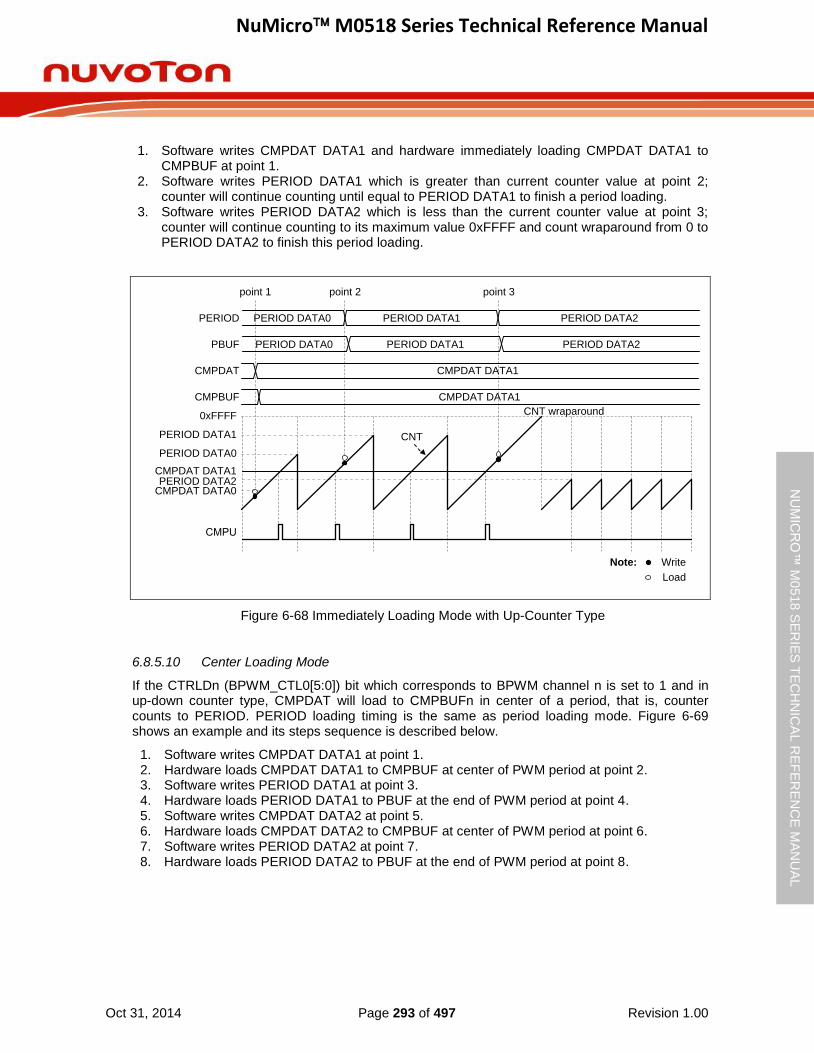
NuMicro M0518 Series Technical Reference Manual
Oct 31, 2014 Page 293 of 497 Revision 1.00
NU
MIC
RO
™ M
0518
SE
RIE
S T
EC
HN
ICA
L R
EF
ER
EN
CE
MA
NU
AL
1. Software writes CMPDAT DATA1 and hardware immediately loading CMPDAT DATA1 to CMPBUF at point 1.
2. Software writes PERIOD DATA1 which is greater than current counter value at point 2; counter will continue counting until equal to PERIOD DATA1 to finish a period loading.
3. Software writes PERIOD DATA2 which is less than the current counter value at point 3; counter will continue counting to its maximum value 0xFFFF and count wraparound from 0 to PERIOD DATA2 to finish this period loading.
CMPDAT DATA0
CMPU
CMPDAT DATA1
PERIOD DATA1
PERIOD DATA2
PERIOD DATA0
CNT
CNT wraparound0xFFFF
Write
Load
Note:
CMPDAT
PERIOD PERIOD DATA0 PERIOD DATA1
CMPDAT DATA1
PBUF PERIOD DATA0 PERIOD DATA1
CMPBUF CMPDAT DATA1
PERIOD DATA2
PERIOD DATA2
point 1 point 2 point 3
Figure 6-68 Immediately Loading Mode with Up-Counter Type
6.8.5.10 Center Loading Mode
If the CTRLDn (BPWM_CTL0[5:0]) bit which corresponds to BPWM channel n is set to 1 and in up-down counter type, CMPDAT will load to CMPBUFn in center of a period, that is, counter counts to PERIOD. PERIOD loading timing is the same as period loading mode. Figure 6-69 shows an example and its steps sequence is described below.
1. Software writes CMPDAT DATA1 at point 1. 2. Hardware loads CMPDAT DATA1 to CMPBUF at center of PWM period at point 2. 3. Software writes PERIOD DATA1 at point 3. 4. Hardware loads PERIOD DATA1 to PBUF at the end of PWM period at point 4. 5. Software writes CMPDAT DATA2 at point 5. 6. Hardware loads CMPDAT DATA2 to CMPBUF at center of PWM period at point 6. 7. Software writes PERIOD DATA2 at point 7. 8. Hardware loads PERIOD DATA2 to PBUF at the end of PWM period at point 8.

NuMicro M0518 Series Technical Reference Manual
Oct 31, 2014 Page 294 of 497 Revision 1.00
NU
MIC
RO
™ M
0518
SE
RIE
S T
EC
HN
ICA
L R
EF
ER
EN
CE
MA
NU
AL
CMPDAT DATA0
CMPU
CMPDAT DATA1
PERIOD DATA0
PERIOD DATA1
PERIOD DATA2
CNT
CMPDAT DATA2
CMPD
Write
Load
Note:
CMPDAT
PERIOD PERIOD DATA0 PERIOD DATA1
CMPDAT DATA1
PBUF PERIOD DATA0 PERIOD DATA1
CMPBUF CMPDAT DATA1
PERIOD DATA2
PERIOD DATA2
CMPDAT DATA0 CMPDAT DATA2
CMPDAT DATA2
point 1 point 2 point 3 point 4 point 5 point 6 point 7 point 8
Figure 6-69 Center Loading Mode with Up-Down-Counter Type
6.8.5.11 BPWM Pulse Generator
BPWM pulse generator uses counter and comparator events to generate BPWM pulse. The events are: zero point, period point in up counter type and down counter type, center point in up-down counter type and counter equal to comparator point in three types. As to up-down counter type, there are two counter equal comparator points, one at up count another at down count.
Each event point can decide BPWM waveform to do nothing (X), set Low (L), set High (H) or toggle (T) by setting BPWM_WGCTL0 and BPWM_WGCTL1 registers. Using these points can easily generate asymmetric BPWM pulse or variant waveform as shown in Figure 6-70. In the figure, there is a comparator n to generate BPWM pulse. n denotes channel number 0 to 5. CMPU denotes CNT is equal to CMPDAT when counting up, CMPD denotes CNT is equal to CMPDAT when counting down.
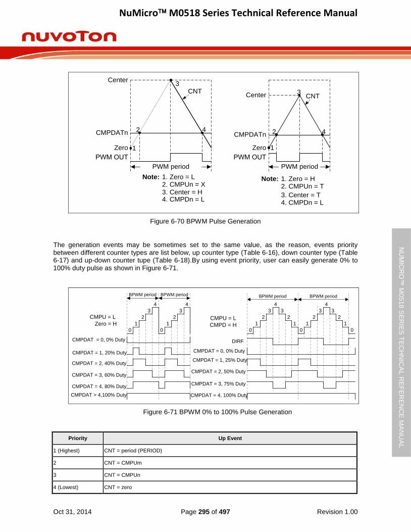
NuMicro M0518 Series Technical Reference Manual
Oct 31, 2014 Page 295 of 497 Revision 1.00
NU
MIC
RO
™ M
0518
SE
RIE
S T
EC
HN
ICA
L R
EF
ER
EN
CE
MA
NU
AL
CNT
PWM period
Zero
CMPDATn
Center
PWM period
CNT
PWM OUT
1
2
3
4
2. CMPUn = X1. Zero = L
4. CMPDn = L3. Center = H
Zero
CMPDATn
Center
2. CMPUn = T1. Zero = H
4. CMPDn = L3. Center = T
Note: Note:
PWM OUT
1
2
3
4
Figure 6-70 BPWM Pulse Generation
The generation events may be sometimes set to the same value, as the reason, events priority between different counter types are list below, up counter type (Table 6-16), down counter type (Table 6-17) and up-down counter tupe (Table 6-18).By using event priority, user can easily generate 0% to 100% duty pulse as shown in Figure 6-71.
0
1
2
3
4
3
2
1
0
1
2
3
4
3
2
1
0
CMPDAT = 0, 0% Duty
CMPDAT = 1, 25% Duty
CMPDAT = 2, 50% Duty
CMPDAT = 3, 75% Duty
CMPDAT = 4, 100% Duty
DIRF
BPWM period BPWM period
0
1
2
3
4
0
1
2
3
4
CMPDAT = 0, 0% Duty
CMPDAT = 1, 20% Duty
CMPDAT = 2, 40% Duty
CMPDAT = 3, 60% Duty
CMPDAT = 4, 80% Duty
CMPDAT > 4,100% Duty
CMPU = L
Zero = H
BPWM period BPWM period
CMPU = L
CMPD = H
Figure 6-71 BPWM 0% to 100% Pulse Generation
Priority Up Event
1 (Highest) CNT = period (PERIOD)
2 CNT = CMPUm
3 CNT = CMPUn
4 (Lowest) CNT = zero
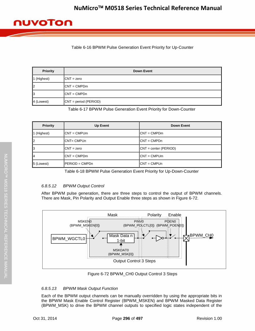
NuMicro M0518 Series Technical Reference Manual
Oct 31, 2014 Page 296 of 497 Revision 1.00
NU
MIC
RO
™ M
0518
SE
RIE
S T
EC
HN
ICA
L R
EF
ER
EN
CE
MA
NU
AL
Table 6-16 BPWM Pulse Generation Event Priority for Up-Counter
Priority Down Event
1 (Highest) CNT = zero
2 CNT = CMPDm
3 CNT = CMPDn
4 (Lowest) CNT = period (PERIOD)
Table 6-17 BPWM Pulse Generation Event Priority for Down-Counter
Priority Up Event Down Event
1 (Highest) CNT = CMPUm CNT = CMPDm
2 CNT= CMPUn CNT = CMPDn
3 CNT = zero CNT = center (PERIOD)
4 CNT = CMPDm CNT = CMPUm
5 (Lowest) PERIOD = CMPDn CNT = CMPUn
Table 6-18 BPWM Pulse Generation Event Priority for Up-Down-Counter
6.8.5.12 BPWM Output Control
After BPWM pulse generation, there are three steps to control the output of BPWM channels. There are Mask, Pin Polarity and Output Enable three steps as shown in Figure 6-72.
Mask Data n
1-bit
MSKDAT0
(BPWM_MSK[0])
PINV0
(BPWM_POLCTL[0])
POEN0
(BPWM_POEN[0])
BPWM_WGCTL0
MSKEN0
(BPWM_MSKEN[0])
BPWM_CH0
Output Control 3 Steps
Mask EnablePolarity
Figure 6-72 BPWM_CH0 Output Control 3 Steps
6.8.5.13 BPWM Mask Output Function
Each of the BPWM output channels can be manually overridden by using the appropriate bits in the BPWM Mask Enable Control Register (BPWM_MSKEN) and BPWM Masked Data Register (BPWM_MSK) to drive the BPWM channel outputs to specified logic states independent of the

NuMicro M0518 Series Technical Reference Manual
Oct 31, 2014 Page 297 of 497 Revision 1.00
NU
MIC
RO
™ M
0518
SE
RIE
S T
EC
HN
ICA
L R
EF
ER
EN
CE
MA
NU
AL
duty cycle comparison units. The BPWM mask bits are useful when controlling various types of Electrically Commutated Motor (ECM) like a BLDC motor. The BPWM_MSKEN register contains six bits, MSKENn(BPWM_MSKEN[5:0]) determine which BPWM channel output will be overridden, MSKENn(BPWM_MSKEN[5:0]) bits are active-high. The BPWM_MSK register contains six bits, MSKDATn(BPWM_MSK[5:0]) determine the state of the BPWM channel output when the channel is masked via the MSKDAT bits. Figure 6-73 shows an example of how BPWM mask control can be used for the override feature.
BPWM_CH2
BPWM_CH0
BPWM_MSK
[5:0]0x8 0x11 0x5
BPWM_MSKEN
[5:0]
BPWM_CH1
BPWM_CH3
0x2A (Mask channel 1, 3, 5) 0x15 (Mask channel 0, 2, 4)
BPWM_CH4
BPWM_CH5
Figure 6-73 Illustration of Mask Control Waveform
6.8.5.14 Polarity Control
Each BPWM port from BPWM_CH0 to BPWM_CH5 has an independent polarity control module to configure the polarity of the active state of BPWM output. By default, the BPWM output is active high. This implies the BPWM OFF state is low and ON state is high. This definition is variable through setting BPWM Negative Polarity Control Register (BPWM_POLCTL), for each individual BPWM channel. Figure 6-74 shows the initial state before BPWM starts with different polarity settings.
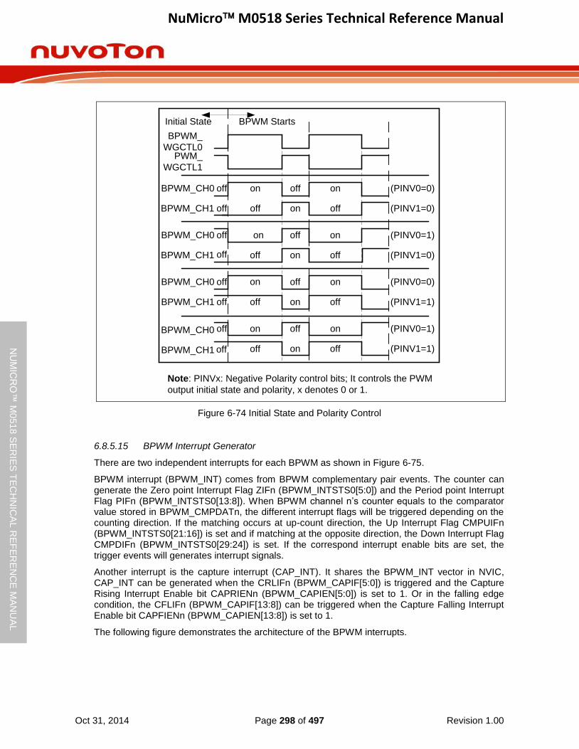
NuMicro M0518 Series Technical Reference Manual
Oct 31, 2014 Page 298 of 497 Revision 1.00
NU
MIC
RO
™ M
0518
SE
RIE
S T
EC
HN
ICA
L R
EF
ER
EN
CE
MA
NU
AL
BPWM_
WGCTL0PWM_
WGCTL1
BPWM_CH0
BPWM_CH1
off on on
off
off
off on off
(PINV0=0)
(PINV1=0)
Note: PINVx: Negative Polarity control bits; It controls the PWM
output initial state and polarity, x denotes 0 or 1.
BPWM_CH0
BPWM_CH1
BPWM_CH0
BPWM_CH1
BPWM_CH0
BPWM_CH1
(PINV0=1)
(PINV1=0)
(PINV0=0)
(PINV1=1)
(PINV0=1)
(PINV1=1)
Initial State BPWM Starts
onoff off on
off off on off
off on onoff
off off on off
off off on off
onoff off on
Figure 6-74 Initial State and Polarity Control
6.8.5.15 BPWM Interrupt Generator
There are two independent interrupts for each BPWM as shown in Figure 6-75.
BPWM interrupt (BPWM_INT) comes from BPWM complementary pair events. The counter can generate the Zero point Interrupt Flag ZIFn (BPWM_INTSTS0[5:0]) and the Period point Interrupt Flag PIFn (BPWM_INTSTS0[13:8]). When BPWM channel n’s counter equals to the comparator value stored in BPWM_CMPDATn, the different interrupt flags will be triggered depending on the counting direction. If the matching occurs at up-count direction, the Up Interrupt Flag CMPUIFn (BPWM_INTSTS0[21:16]) is set and if matching at the opposite direction, the Down Interrupt Flag CMPDIFn (BPWM_INTSTS0[29:24]) is set. If the correspond interrupt enable bits are set, the trigger events will generates interrupt signals.
Another interrupt is the capture interrupt (CAP_INT). It shares the BPWM_INT vector in NVIC, CAP_INT can be generated when the CRLIFn (BPWM_CAPIF[5:0]) is triggered and the Capture Rising Interrupt Enable bit CAPRIENn (BPWM_CAPIEN[5:0]) is set to 1. Or in the falling edge condition, the CFLIFn (BPWM_CAPIF[13:8]) can be triggered when the Capture Falling Interrupt Enable bit CAPFIENn (BPWM_CAPIEN[13:8]) is set to 1.
The following figure demonstrates the architecture of the BPWM interrupts.
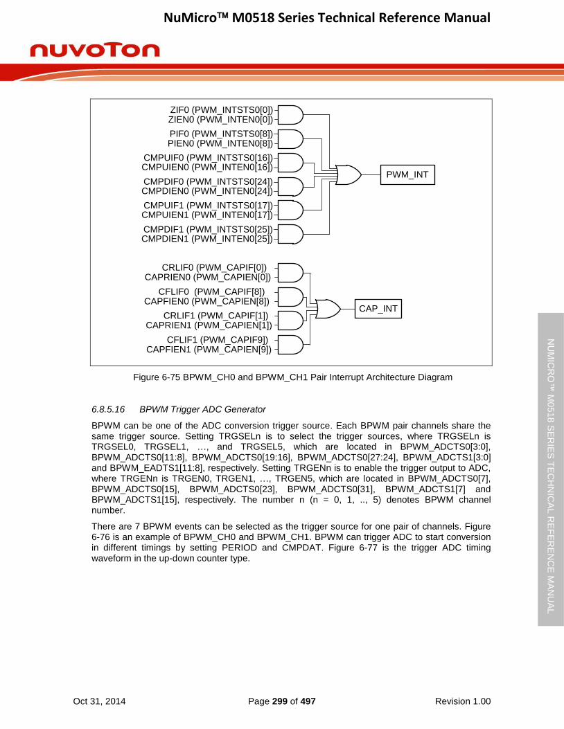
NuMicro M0518 Series Technical Reference Manual
Oct 31, 2014 Page 299 of 497 Revision 1.00
NU
MIC
RO
™ M
0518
SE
RIE
S T
EC
HN
ICA
L R
EF
ER
EN
CE
MA
NU
AL
CRLIF0 (PWM_CAPIF[0])
PWM_INT
CAP_INT
ZIEN0 (PWM_INTEN0[0])ZIF0 (PWM_INTSTS0[0])
PIEN0 (PWM_INTEN0[8])PIF0 (PWM_INTSTS0[8])
CMPUIEN0 (PWM_INTEN0[16])CMPUIF0 (PWM_INTSTS0[16])
CMPDIEN0 (PWM_INTEN0[24])CMPDIF0 (PWM_INTSTS0[24])
CMPUIEN1 (PWM_INTEN0[17])CMPUIF1 (PWM_INTSTS0[17])
CMPDIEN1 (PWM_INTEN0[25])CMPDIF1 (PWM_INTSTS0[25])
CAPRIEN0 (PWM_CAPIEN[0])
CFLIF0 (PWM_CAPIF[8])CAPFIEN0 (PWM_CAPIEN[8])
CRLIF1 (PWM_CAPIF[1])CAPRIEN1 (PWM_CAPIEN[1])
CFLIF1 (PWM_CAPIF9])CAPFIEN1 (PWM_CAPIEN[9])
Figure 6-75 BPWM_CH0 and BPWM_CH1 Pair Interrupt Architecture Diagram
6.8.5.16 BPWM Trigger ADC Generator
BPWM can be one of the ADC conversion trigger source. Each BPWM pair channels share the same trigger source. Setting TRGSELn is to select the trigger sources, where TRGSELn is TRGSEL0, TRGSEL1, …, and TRGSEL5, which are located in BPWM_ADCTS0[3:0], BPWM_ADCTS0[11:8], BPWM_ADCTS0[19:16], BPWM_ADCTS0[27:24], BPWM_ADCTS1[3:0] and BPWM_EADTS1[11:8], respectively. Setting TRGENn is to enable the trigger output to ADC, where TRGENn is TRGEN0, TRGEN1, …, TRGEN5, which are located in BPWM_ADCTS0[7], BPWM_ADCTS0[15], BPWM_ADCTS0[23], BPWM_ADCTS0[31], BPWM_ADCTS1[7] and BPWM_ADCTS1[15], respectively. The number n (n = 0, 1, .., 5) denotes BPWM channel number.
There are 7 BPWM events can be selected as the trigger source for one pair of channels. Figure 6-76 is an example of BPWM_CH0 and BPWM_CH1. BPWM can trigger ADC to start conversion in different timings by setting PERIOD and CMPDAT. Figure 6-77 is the trigger ADC timing waveform in the up-down counter type.
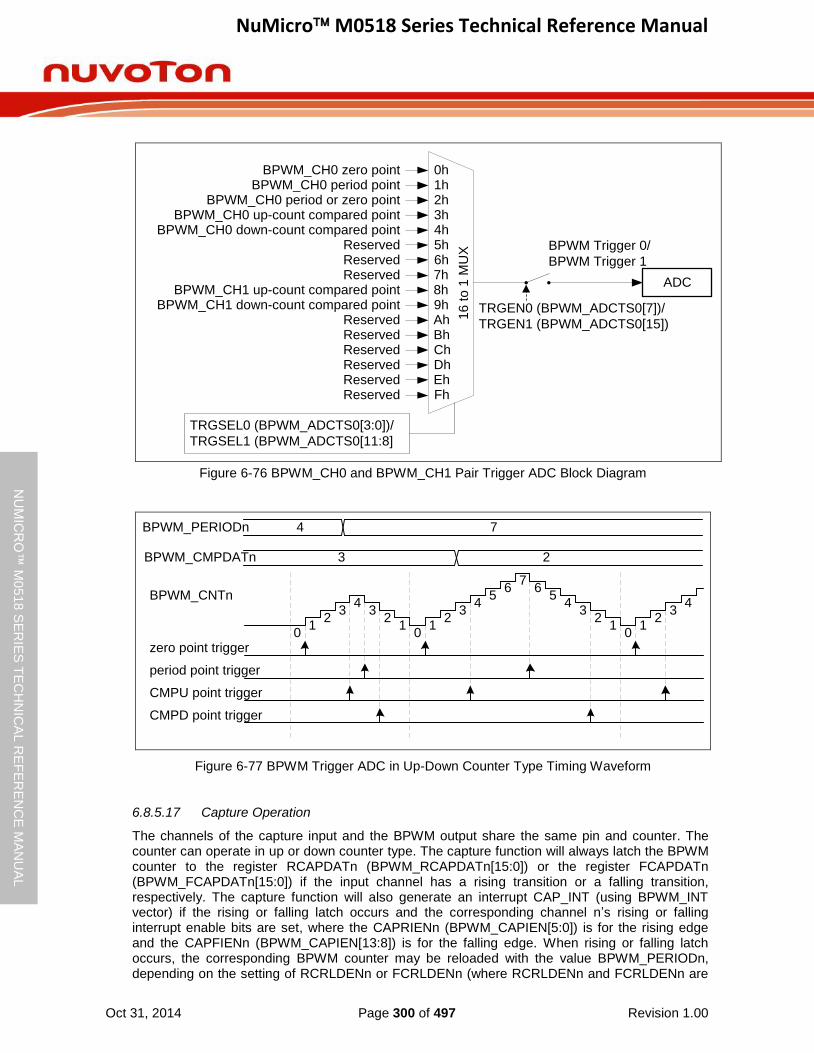
NuMicro M0518 Series Technical Reference Manual
Oct 31, 2014 Page 300 of 497 Revision 1.00
NU
MIC
RO
™ M
0518
SE
RIE
S T
EC
HN
ICA
L R
EF
ER
EN
CE
MA
NU
AL
16
to
1 M
UX
2h3h
0h1h
6h7h
4h5h
Fh
BPWM_CH1 down-count compared point
BPWM_CH0 zero pointBPWM_CH0 period point
BPWM_CH0 up-count compared pointBPWM_CH0 down-count compared point
BPWM_CH1 up-count compared point
BPWM Trigger 0/
BPWM Trigger 1
Reserved9hAh
8h
DhEh
BhCh
TRGSEL0 (BPWM_ADCTS0[3:0])/
TRGSEL1 (BPWM_ADCTS0[11:8]
TRGEN0 (BPWM_ADCTS0[7])/
TRGEN1 (BPWM_ADCTS0[15])
BPWM_CH0 period or zero point
ADC
ReservedReservedReservedReservedReserved
ReservedReservedReserved
Figure 6-76 BPWM_CH0 and BPWM_CH1 Pair Trigger ADC Block Diagram
BPWM_CMPDATn
BPWM_PERIODn
zero point trigger
BPWM_CNTn
4 7
3 2
01
23
43
12
01
23
43
12
0
56
76
45
12
34
period point trigger
CMPU point trigger
CMPD point trigger
Figure 6-77 BPWM Trigger ADC in Up-Down Counter Type Timing Waveform
6.8.5.17 Capture Operation
The channels of the capture input and the BPWM output share the same pin and counter. The counter can operate in up or down counter type. The capture function will always latch the BPWM counter to the register RCAPDATn (BPWM_RCAPDATn[15:0]) or the register FCAPDATn (BPWM_FCAPDATn[15:0]) if the input channel has a rising transition or a falling transition, respectively. The capture function will also generate an interrupt CAP_INT (using BPWM_INT vector) if the rising or falling latch occurs and the corresponding channel n’s rising or falling interrupt enable bits are set, where the CAPRIENn (BPWM_CAPIEN[5:0]) is for the rising edge and the CAPFIENn (BPWM_CAPIEN[13:8]) is for the falling edge. When rising or falling latch occurs, the corresponding BPWM counter may be reloaded with the value BPWM_PERIODn, depending on the setting of RCRLDENn or FCRLDENn (where RCRLDENn and FCRLDENn are

NuMicro M0518 Series Technical Reference Manual
Oct 31, 2014 Page 301 of 497 Revision 1.00
NU
MIC
RO
™ M
0518
SE
RIE
S T
EC
HN
ICA
L R
EF
ER
EN
CE
MA
NU
AL
located at BPWM_CAPCTL[21:16] and BPWM_CAPCTL[29:24], respectively). Note that the corresponding GPIO pins must be configured as the capture function by enable the CAPINENn (BPWM_CAPINEN[5:0]) for the corresponding capture channel n. Figure 6-78 is the capture block diagram of channel 0.
0
1
16-bits BPWM
up/down counter CNT
(BPWM_CNT0[15:0])
DIRF
(BPWM_CNT0[16])
PERIOD
(BPWM_PERIOD0)
RCAPPAT
(BPWM_RCAPDAT0[15:0])
FCAPDAT
(BPWM_FCAPDAT0[15:0])
CAPEN0
(BPWM_CAPCTL[0])CAPINV0
(BPWM_CAPCTL[8])
CAPINEN0
(BPWM_CAPINEN[0])
BPWM_CH0
RCRLDEN0
(BPWM_CAPCTL[16])
FCRLDEN0
(BPWM_CAPCTL[24])
Note: denotes rising edge detect
denotes falling edge detect
Rising Latch
Falling Latch
BPWM_CH1~5
Reload signal
Figure 6-78 BPWM_CH0 Capture Block Diagram
Figure 6-79 illustrates the capture function timing. In this case, the capture counter is set as BPWM down counter type and the PERIOD is set to 8 so that the counter counts in the down direction, from 8 to 0. When detecting a falling edge at the capture input pin, the capture function latches counter value to the BPWM_FCAPDATn. When detecting the rising edge, it latches the counter value to the BPWM_RCAPDATn. In this timing diagram, when the falling edge is detected at the first time, the capture function will reload the counter value from the PERIOD setting because the FCRLDENn is enabled. But at the second time, the falling edge does not result in a reload because of the disabled FCRLDENn. In this example, the counter also reloads at the rising edge of the capture input because the RCRLDENn is enabled, too.
Moreover, if the case is setup as the up counter type, the counter will reload the value zero and count up to the value PERIOD. It is important that the counter is shared by all channels, so the counter reloads time also controlled by all channels’ reload signals.
Figure 6-79 also illustrates the timing example for the interrupt and interrupt flag generation. When the rising edge at channel n is detected, the corresponding bit CRLIFn (BPWM_CAPIF[5:0]) is set by hardware. Similarly, a falling edge detection at chnnel n causes the corresponding bit CFLIFn (BPWM_CAPIF[13:8]) set by hardware. CRLIFn and CFLIFn can be cleared by software by writing ‘1’. If the CRLIFn is set and the CAPRIENn is enabled, the capture function generates an interrupt. If the CFLIFn is set and the CAPFIENn is enabled, the interrupt
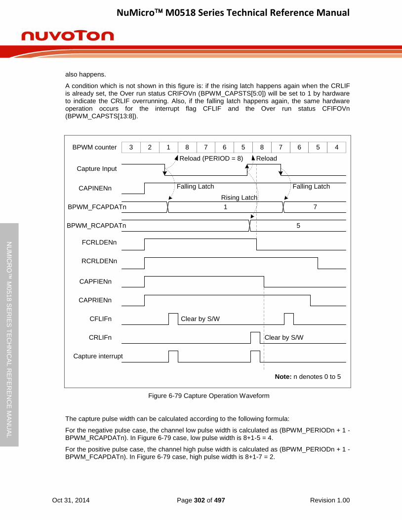
NuMicro M0518 Series Technical Reference Manual
Oct 31, 2014 Page 302 of 497 Revision 1.00
NU
MIC
RO
™ M
0518
SE
RIE
S T
EC
HN
ICA
L R
EF
ER
EN
CE
MA
NU
AL
also happens.
A condition which is not shown in this figure is: if the rising latch happens again when the CRLIF is already set, the Over run status CRIFOVn (BPWM_CAPSTS[5:0]) will be set to 1 by hardware to indicate the CRLIF overrunning. Also, if the falling latch happens again, the same hardware operation occurs for the interrupt flag CFLIF and the Over run status CFIFOVn (BPWM_CAPSTS[13:8]).
Note: n denotes 0 to 5
8 7 6 5 43 2 1 8 7 6 5BPWM counter
1 7
Capture Input
BPWM_FCAPDATn
5BPWM_RCAPDATn
Capture interrupt
CAPFIENn
CAPRIENn
CAPINENn
Clear by S/WCFLIFn
CRLIFn
Reload (PERIOD = 8) Reload
Clear by S/W
Falling Latch Falling Latch
Rising Latch
FCRLDENn
RCRLDENn
Figure 6-79 Capture Operation Waveform
The capture pulse width can be calculated according to the following formula:
For the negative pulse case, the channel low pulse width is calculated as (BPWM_PERIODn + 1 - BPWM_RCAPDATn). In Figure 6-79 case, low pulse width is 8+1-5 = 4.
For the positive pulse case, the channel high pulse width is calculated as (BPWM_PERIODn + 1 - BPWM_FCAPDATn). In Figure 6-79 case, high pulse width is 8+1-7 = 2.
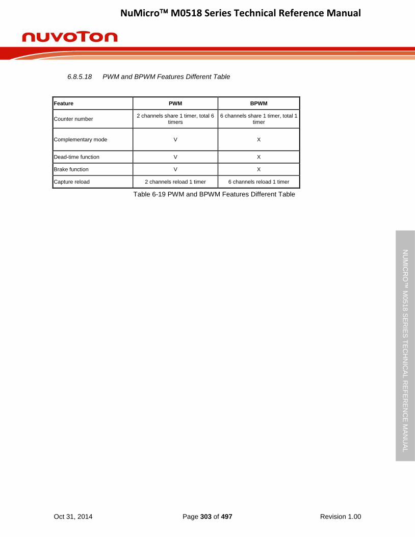
NuMicro M0518 Series Technical Reference Manual
Oct 31, 2014 Page 303 of 497 Revision 1.00
NU
MIC
RO
™ M
0518
SE
RIE
S T
EC
HN
ICA
L R
EF
ER
EN
CE
MA
NU
AL
6.8.5.18 PWM and BPWM Features Different Table
Feature PWM BPWM
Counter number 2 channels share 1 timer, total 6
timers 6 channels share 1 timer, total 1
timer
Complementary mode V X
Dead-time function V X
Brake function V X
Capture reload 2 channels reload 1 timer 6 channels reload 1 timer
Table 6-19 PWM and BPWM Features Different Table
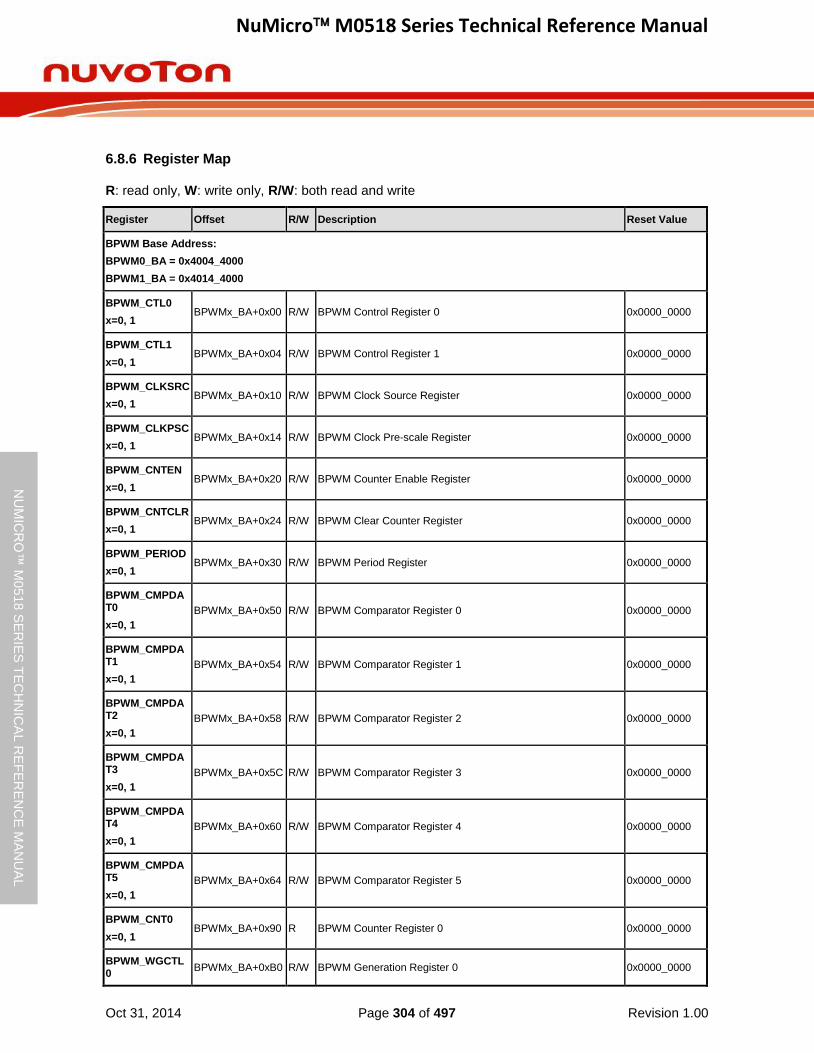
NuMicro M0518 Series Technical Reference Manual
Oct 31, 2014 Page 304 of 497 Revision 1.00
NU
MIC
RO
™ M
0518
SE
RIE
S T
EC
HN
ICA
L R
EF
ER
EN
CE
MA
NU
AL
6.8.6 Register Map
R: read only, W: write only, R/W: both read and write
Register Offset R/W Description Reset Value
BPWM Base Address:
BPWM0_BA = 0x4004_4000
BPWM1_BA = 0x4014_4000
BPWM_CTL0
x=0, 1 BPWMx_BA+0x00 R/W BPWM Control Register 0 0x0000_0000
BPWM_CTL1
x=0, 1 BPWMx_BA+0x04 R/W BPWM Control Register 1 0x0000_0000
BPWM_CLKSRC
x=0, 1 BPWMx_BA+0x10 R/W BPWM Clock Source Register 0x0000_0000
BPWM_CLKPSC
x=0, 1 BPWMx_BA+0x14 R/W BPWM Clock Pre-scale Register 0x0000_0000
BPWM_CNTEN
x=0, 1 BPWMx_BA+0x20 R/W BPWM Counter Enable Register 0x0000_0000
BPWM_CNTCLR
x=0, 1 BPWMx_BA+0x24 R/W BPWM Clear Counter Register 0x0000_0000
BPWM_PERIOD
x=0, 1 BPWMx_BA+0x30 R/W BPWM Period Register 0x0000_0000
BPWM_CMPDAT0
x=0, 1
BPWMx_BA+0x50 R/W BPWM Comparator Register 0 0x0000_0000
BPWM_CMPDAT1
x=0, 1
BPWMx_BA+0x54 R/W BPWM Comparator Register 1 0x0000_0000
BPWM_CMPDAT2
x=0, 1
BPWMx_BA+0x58 R/W BPWM Comparator Register 2 0x0000_0000
BPWM_CMPDAT3
x=0, 1
BPWMx_BA+0x5C R/W BPWM Comparator Register 3 0x0000_0000
BPWM_CMPDAT4
x=0, 1
BPWMx_BA+0x60 R/W BPWM Comparator Register 4 0x0000_0000
BPWM_CMPDAT5
x=0, 1
BPWMx_BA+0x64 R/W BPWM Comparator Register 5 0x0000_0000
BPWM_CNT0
x=0, 1 BPWMx_BA+0x90 R BPWM Counter Register 0 0x0000_0000
BPWM_WGCTL0
BPWMx_BA+0xB0 R/W BPWM Generation Register 0 0x0000_0000
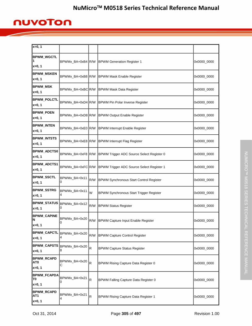
NuMicro M0518 Series Technical Reference Manual
Oct 31, 2014 Page 305 of 497 Revision 1.00
NU
MIC
RO
™ M
0518
SE
RIE
S T
EC
HN
ICA
L R
EF
ER
EN
CE
MA
NU
AL
x=0, 1
BPWM_WGCTL1
x=0, 1
BPWMx_BA+0xB4 R/W BPWM Generation Register 1 0x0000_0000
BPWM_MSKEN
x=0, 1 BPWMx_BA+0xB8 R/W BPWM Mask Enable Register 0x0000_0000
BPWM_MSK
x=0, 1 BPWMx_BA+0xBC R/W BPWM Mask Data Register 0x0000_0000
BPWM_POLCTL
x=0, 1 BPWMx_BA+0xD4 R/W BPWM Pin Polar Inverse Register 0x0000_0000
BPWM_POEN
x=0, 1 BPWMx_BA+0xD8 R/W BPWM Output Enable Register 0x0000_0000
BPWM_INTEN
x=0, 1 BPWMx_BA+0xE0 R/W BPWM Interrupt Enable Register 0x0000_0000
BPWM_INTSTS
x=0, 1 BPWMx_BA+0xE8 R/W BPWM Interrupt Flag Register 0x0000_0000
BPWM_ADCTS0
x=0, 1 BPWMx_BA+0xF8 R/W BPWM Trigger ADC Source Select Register 0 0x0000_0000
BPWM_ADCTS1
x=0, 1 BPWMx_BA+0xFC R/W BPWM Trigger ADC Source Select Register 1 0x0000_0000
BPWM_SSCTL
x=0, 1
BPWMx_BA+0x110
R/W BPWM Synchronous Start Control Register 0x0000_0000
BPWM_SSTRG
x=0, 1
BPWMx_BA+0x114
W BPWM Synchronous Start Trigger Register 0x0000_0000
BPWM_STATUS
x=0, 1
BPWMx_BA+0x120
R/W BPWM Status Register 0x0000_0000
BPWM_CAPINEN
x=0, 1
BPWMx_BA+0x200
R/W BPWM Capture Input Enable Register 0x0000_0000
BPWM_CAPCTL
x=0, 1
BPWMx_BA+0x204
R/W BPWM Capture Control Register 0x0000_0000
BPWM_CAPSTS
x=0, 1
BPWMx_BA+0x208
R BPWM Capture Status Register 0x0000_0000
BPWM_RCAPDAT0
x=0, 1
BPWMx_BA+0x20C
R BPWM Rising Capture Data Register 0 0x0000_0000
BPWM_FCAPDAT0
x=0, 1
BPWMx_BA+0x210
R BPWM Falling Capture Data Register 0 0x0000_0000
BPWM_RCAPDAT1
x=0, 1
BPWMx_BA+0x214
R BPWM Rising Capture Data Register 1 0x0000_0000

NuMicro M0518 Series Technical Reference Manual
Oct 31, 2014 Page 306 of 497 Revision 1.00
NU
MIC
RO
™ M
0518
SE
RIE
S T
EC
HN
ICA
L R
EF
ER
EN
CE
MA
NU
AL
BPWM_FCAPDAT1
x=0, 1
BPWMx_BA+0x218
R BPWM Falling Capture Data Register 1 0x0000_0000
BPWM_RCAPDAT2
x=0, 1
BPWMx_BA+0x21C
R BPWM Rising Capture Data Register 2 0x0000_0000
BPWM_FCAPDAT2
x=0, 1
BPWMx_BA+0x220
R BPWM Falling Capture Data Register 2 0x0000_0000
BPWM_RCAPDAT3
x=0, 1
BPWMx_BA+0x224
R BPWM Rising Capture Data Register 3 0x0000_0000
BPWM_FCAPDAT3
x=0, 1
BPWMx_BA+0x228
R BPWM Falling Capture Data Register 3 0x0000_0000
BPWM_RCAPDAT4
x=0, 1
BPWMx_BA+0x22C
R BPWM Rising Capture Data Register 4 0x0000_0000
BPWM_FCAPDAT4
x=0, 1
BPWMx_BA+0x230
R BPWM Falling Capture Data Register 4 0x0000_0000
BPWM_RCAPDAT5
x=0, 1
BPWMx_BA+0x234
R BPWM Rising Capture Data Register 5 0x0000_0000
BPWM_FCAPDAT5
x=0, 1
BPWMx_BA+0x238
R BPWM Falling Capture Data Register 5 0x0000_0000
BPWM_CAPIEN
x=0, 1
BPWMx_BA+0x250
R/W BPWM Capture Interrupt Enable Register 0x0000_0000
BPWM_CAPIF
x=0, 1
BPWMx_BA+0x254
R/W BPWM Capture Interrupt Flag Register 0x0000_0000
BPWM_PBUF
x=0, 1
BPWMx_BA+0x304
R BPWM PERIOD Buffer 0x0000_0000
BPWM_CMPBUF0
x=0, 1
BPWMx_BA+0x31C
R BPWM CMPDAT0 Buffer 0x0000_0000
BPWM_CMPBUF1
x=0, 1
BPWMx_BA+0x320
R BPWM CMPDAT1 Buffer 0x0000_0000
BPWM_CMPBUF2
x=0, 1
BPWMx_BA+0x324
R BPWM CMPDAT 2 Buffer 0x0000_0000
BPWM_CMPBUF3
x=0, 1
BPWMx_BA+0x328
R BPWM CMPDAT 3 Buffer 0x0000_0000
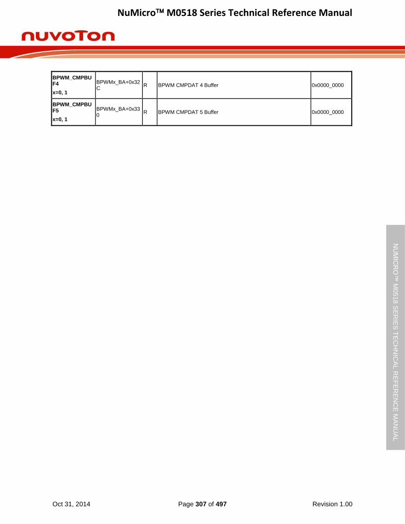
NuMicro M0518 Series Technical Reference Manual
Oct 31, 2014 Page 307 of 497 Revision 1.00
NU
MIC
RO
™ M
0518
SE
RIE
S T
EC
HN
ICA
L R
EF
ER
EN
CE
MA
NU
AL
BPWM_CMPBUF4
x=0, 1
BPWMx_BA+0x32C
R BPWM CMPDAT 4 Buffer 0x0000_0000
BPWM_CMPBUF5
x=0, 1
BPWMx_BA+0x330
R BPWM CMPDAT 5 Buffer 0x0000_0000

NuMicro M0518 Series Technical Reference Manual
Oct 31, 2014 Page 308 of 497 Revision 1.00
NU
MIC
RO
™ M
0518
SE
RIE
S T
EC
HN
ICA
L R
EF
ER
EN
CE
MA
NU
AL
6.8.7 Register Description
BPWM Control Register 0 (BPWM_CTL0)
Register Offset R/W Description Reset Value
BPWM_CTL0 BPWMx_BA+0x00 R/W BPWM Control Register 0 0x0000_0000
31 30 29 28 27 26 25 24
DBGTRIOFF DBGHALT Reserved
23 22 21 20 19 18 17 16
Reserved IMMLDEN5 IMMLDEN4 IMMLDEN3 IMMLDEN2 IMMLDEN1 IMMLDEN0
15 14 13 12 11 10 9 8
Reserved
7 6 5 4 3 2 1 0
Reserved CTRLD5 CTRLD4 CTRLD3 CTRLD2 CTRLD1 CTRLD0
Bits Description
[31] DBGTRIOFF
ICE Debug Mode Acknowledge Disable (Write Protect)
0 = ICE debug mode acknowledgement effects BPWM output.
BPWM pin will be forced as tri-state while ICE debug mode acknowledged.
1 = ICE debug mode acknowledgement disabled.
BPWM pin will keep output no matter ICE debug mode acknowledged or not.
Note: This register is write protected. Refer to SYS_REGLCTL register.
[30] DBGHALT
ICE Debug Mode Counter Halt (Write Protect)
If counter halt is enabled, BPWM all counters will keep current value until exit ICE debug mode.
0 = ICE debug mode counter halt disable.
1 = ICE debug mode counter halt enable.
Note: This register is write protected. Refer to SYS_REGLCTL register.
[29:22] Reserved Reserved.
[21:16] IMMLDENn
Immediately Load Enable Control
Each bit n controls the corresponding BPWM channel n.
0 = PERIOD will load to PBUF at the end point of each period. CMPDAT will load to CMPBUF at the end point or center point of each period by setting CTRLD bit.
1 = PERIOD/CMPDAT will load to PBUF and CMPBUF immediately when software update PERIOD/CMPDAT.
Note: If IMMLDENn is enabled, WINLDENn and CTRLDn will be invalid.
[15:6] Reserved Reserved.
[5:0] CTRLDn
Center Re-Load
Each bit n controls the corresponding BPWM channel n.
In up-down counter type, PERIOD will load to PBUF at the end point of each period.

NuMicro M0518 Series Technical Reference Manual
Oct 31, 2014 Page 309 of 497 Revision 1.00
NU
MIC
RO
™ M
0518
SE
RIE
S T
EC
HN
ICA
L R
EF
ER
EN
CE
MA
NU
AL
CMPDAT will load to CMPBUF at the center point of a period.

NuMicro M0518 Series Technical Reference Manual
Oct 31, 2014 Page 310 of 497 Revision 1.00
NU
MIC
RO
™ M
0518
SE
RIE
S T
EC
HN
ICA
L R
EF
ER
EN
CE
MA
NU
AL
BPWM Control Register 1 (BPWM_CTL1)
Register Offset R/W Description Reset Value
BPWM_CTL1 BPWMx_BA+0x04 R/W BPWM Control Register 1 0x0000_0000
31 30 29 28 27 26 25 24
Reserved
23 22 21 20 19 18 17 16
Reserved
15 14 13 12 11 10 9 8
Reserved
7 6 5 4 3 2 1 0
Reserved CNTTYPE0
Bits Description
[31:2] Reserved Reserved.
[1:0] CNTTYPE0
BPWM Counter Behavior Type 0
Each bit n controls corresponding BPWM channel n.
00 = Up counter type (supports in capture mode).
01 = Down count type (supports in capture mode).
10 = Up-down counter type.
11 = Reserved.
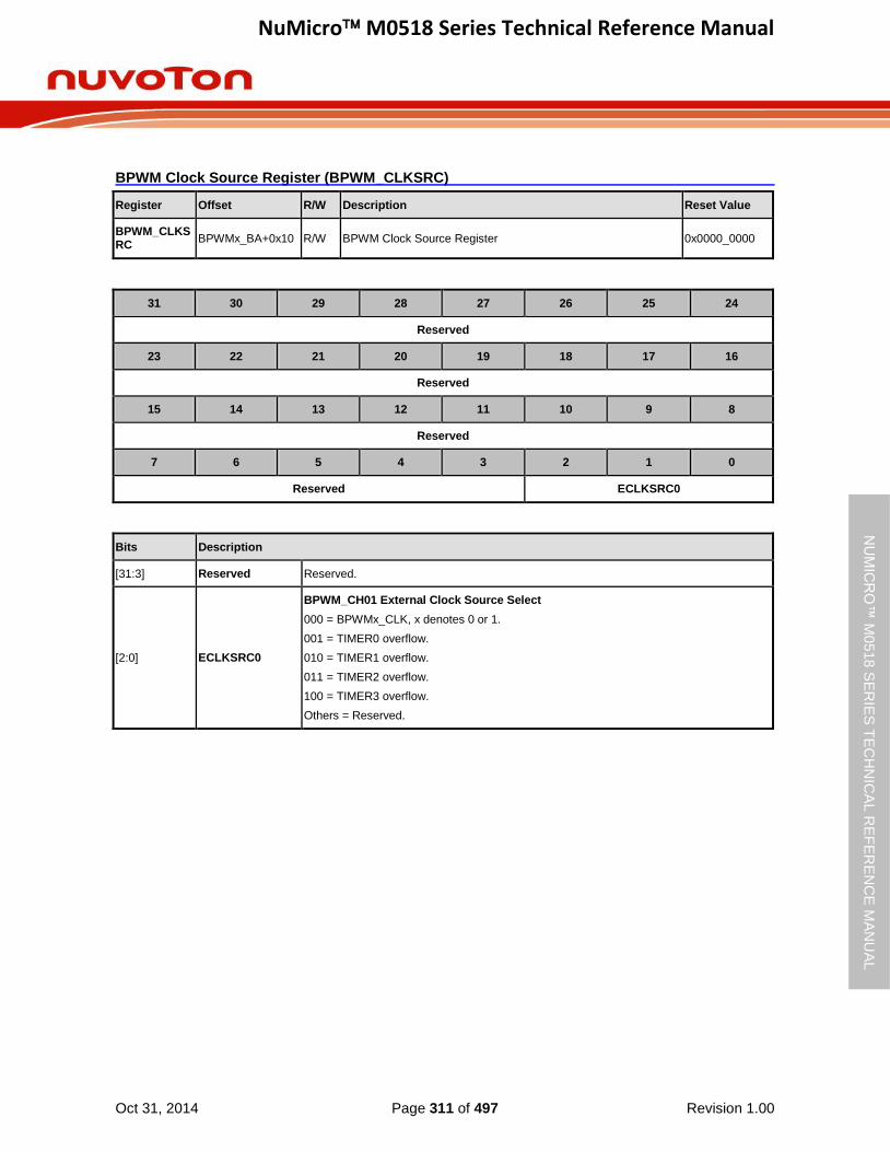
NuMicro M0518 Series Technical Reference Manual
Oct 31, 2014 Page 311 of 497 Revision 1.00
NU
MIC
RO
™ M
0518
SE
RIE
S T
EC
HN
ICA
L R
EF
ER
EN
CE
MA
NU
AL
BPWM Clock Source Register (BPWM_CLKSRC)
Register Offset R/W Description Reset Value
BPWM_CLKSRC
BPWMx_BA+0x10 R/W BPWM Clock Source Register 0x0000_0000
31 30 29 28 27 26 25 24
Reserved
23 22 21 20 19 18 17 16
Reserved
15 14 13 12 11 10 9 8
Reserved
7 6 5 4 3 2 1 0
Reserved ECLKSRC0
Bits Description
[31:3] Reserved Reserved.
[2:0] ECLKSRC0
BPWM_CH01 External Clock Source Select
000 = BPWMx_CLK, x denotes 0 or 1.
001 = TIMER0 overflow.
010 = TIMER1 overflow.
011 = TIMER2 overflow.
100 = TIMER3 overflow.
Others = Reserved.

NuMicro M0518 Series Technical Reference Manual
Oct 31, 2014 Page 312 of 497 Revision 1.00
NU
MIC
RO
™ M
0518
SE
RIE
S T
EC
HN
ICA
L R
EF
ER
EN
CE
MA
NU
AL
BPWM Clock Pre-Scale Register (BPWM_CLKPSC)
Register Offset R/W Description Reset Value
BPWM_CLKPSC
BPWMx_BA+0x14 R/W BPWM Clock Pre-scale Register 0x0000_0000
31 30 29 28 27 26 25 24
Reserved
23 22 21 20 19 18 17 16
Reserved
15 14 13 12 11 10 9 8
Reserved CLKPSC
7 6 5 4 3 2 1 0
CLKPSC
Bits Description
[31:12] Reserved Reserved.
[11:0] CLKPSC
BPWM Counter Clock Pre-Scale
The clock of BPWM counter is decided by clock prescaler. Each BPWM pair share one BPWM counter clock prescaler. The clock of BPWM counter is divided by (CLKPSC+ 1).
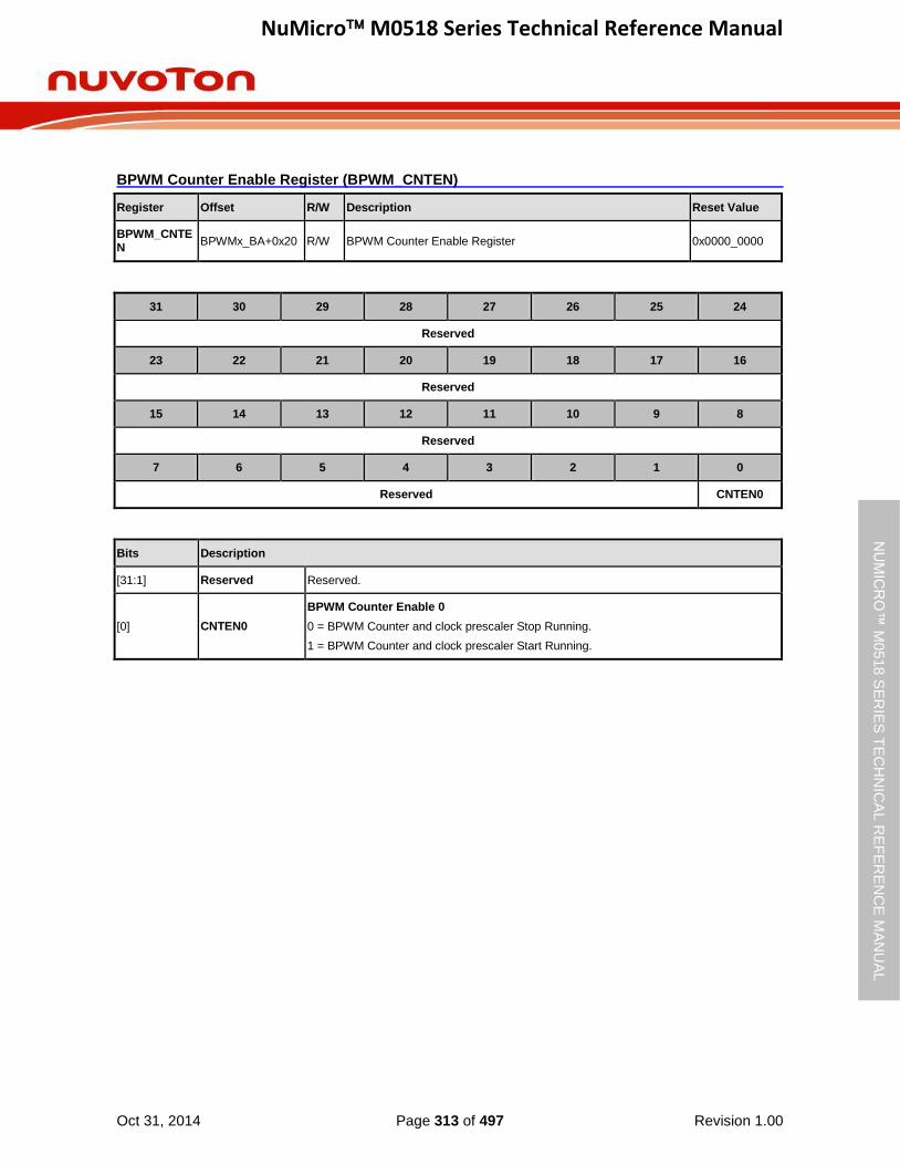
NuMicro M0518 Series Technical Reference Manual
Oct 31, 2014 Page 313 of 497 Revision 1.00
NU
MIC
RO
™ M
0518
SE
RIE
S T
EC
HN
ICA
L R
EF
ER
EN
CE
MA
NU
AL
BPWM Counter Enable Register (BPWM_CNTEN)
Register Offset R/W Description Reset Value
BPWM_CNTEN
BPWMx_BA+0x20 R/W BPWM Counter Enable Register 0x0000_0000
31 30 29 28 27 26 25 24
Reserved
23 22 21 20 19 18 17 16
Reserved
15 14 13 12 11 10 9 8
Reserved
7 6 5 4 3 2 1 0
Reserved CNTEN0
Bits Description
[31:1] Reserved Reserved.
[0] CNTEN0
BPWM Counter Enable 0
0 = BPWM Counter and clock prescaler Stop Running.
1 = BPWM Counter and clock prescaler Start Running.

NuMicro M0518 Series Technical Reference Manual
Oct 31, 2014 Page 314 of 497 Revision 1.00
NU
MIC
RO
™ M
0518
SE
RIE
S T
EC
HN
ICA
L R
EF
ER
EN
CE
MA
NU
AL
BPWM Clear Counter Register (BPWM_CNTCLR)
Register Offset R/W Description Reset Value
BPWM_CNTCLR
BPWMx_BA+0x24 R/W BPWM Clear Counter Register 0x0000_0000
31 30 29 28 27 26 25 24
Reserved
23 22 21 20 19 18 17 16
Reserved
15 14 13 12 11 10 9 8
Reserved
7 6 5 4 3 2 1 0
Reserved CNTCLR0
Bits Description
[31:1] Reserved Reserved.
[0] CNTCLR0
Clear BPWM Counter Control Bit 0
It is automatically cleared by hardware.
0 = No effect.
1 = Clear 16-bit BPWM counter to 0000H.
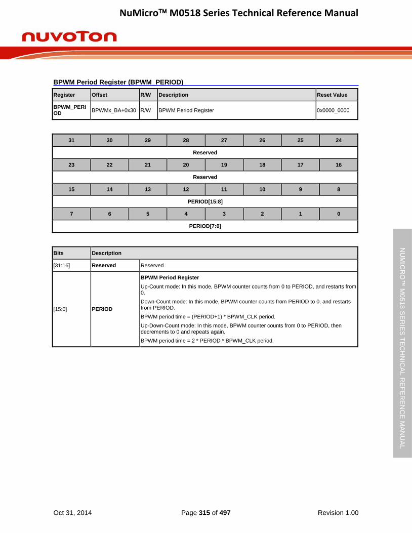
NuMicro M0518 Series Technical Reference Manual
Oct 31, 2014 Page 315 of 497 Revision 1.00
NU
MIC
RO
™ M
0518
SE
RIE
S T
EC
HN
ICA
L R
EF
ER
EN
CE
MA
NU
AL
BPWM Period Register (BPWM_PERIOD)
Register Offset R/W Description Reset Value
BPWM_PERIOD
BPWMx_BA+0x30 R/W BPWM Period Register 0x0000_0000
31 30 29 28 27 26 25 24
Reserved
23 22 21 20 19 18 17 16
Reserved
15 14 13 12 11 10 9 8
PERIOD[15:8]
7 6 5 4 3 2 1 0
PERIOD[7:0]
Bits Description
[31:16] Reserved Reserved.
[15:0] PERIOD
BPWM Period Register
Up-Count mode: In this mode, BPWM counter counts from 0 to PERIOD, and restarts from 0.
Down-Count mode: In this mode, BPWM counter counts from PERIOD to 0, and restarts from PERIOD.
BPWM period time = (PERIOD+1) * BPWM_CLK period.
Up-Down-Count mode: In this mode, BPWM counter counts from 0 to PERIOD, then decrements to 0 and repeats again.
BPWM period time = 2 * PERIOD * BPWM_CLK period.
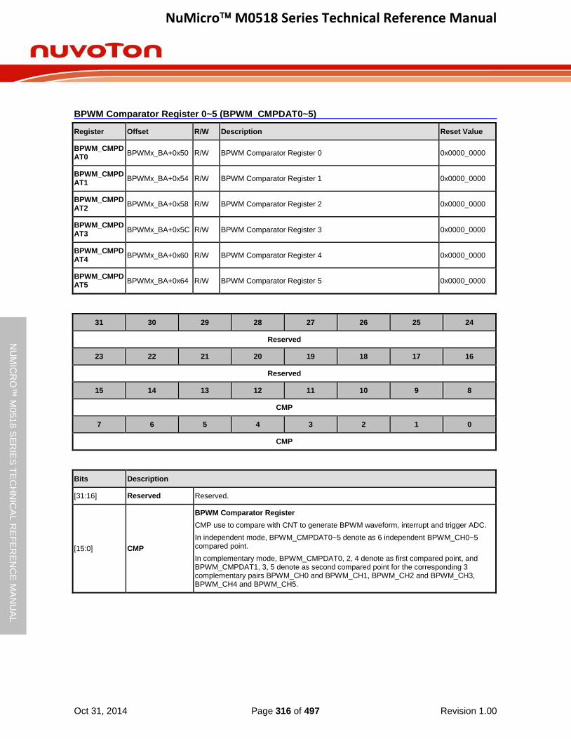
NuMicro M0518 Series Technical Reference Manual
Oct 31, 2014 Page 316 of 497 Revision 1.00
NU
MIC
RO
™ M
0518
SE
RIE
S T
EC
HN
ICA
L R
EF
ER
EN
CE
MA
NU
AL
BPWM Comparator Register 0~5 (BPWM_CMPDAT0~5)
Register Offset R/W Description Reset Value
BPWM_CMPDAT0
BPWMx_BA+0x50 R/W BPWM Comparator Register 0 0x0000_0000
BPWM_CMPDAT1
BPWMx_BA+0x54 R/W BPWM Comparator Register 1 0x0000_0000
BPWM_CMPDAT2
BPWMx_BA+0x58 R/W BPWM Comparator Register 2 0x0000_0000
BPWM_CMPDAT3
BPWMx_BA+0x5C R/W BPWM Comparator Register 3 0x0000_0000
BPWM_CMPDAT4
BPWMx_BA+0x60 R/W BPWM Comparator Register 4 0x0000_0000
BPWM_CMPDAT5
BPWMx_BA+0x64 R/W BPWM Comparator Register 5 0x0000_0000
31 30 29 28 27 26 25 24
Reserved
23 22 21 20 19 18 17 16
Reserved
15 14 13 12 11 10 9 8
CMP
7 6 5 4 3 2 1 0
CMP
Bits Description
[31:16] Reserved Reserved.
[15:0] CMP
BPWM Comparator Register
CMP use to compare with CNT to generate BPWM waveform, interrupt and trigger ADC.
In independent mode, BPWM_CMPDAT0~5 denote as 6 independent BPWM_CH0~5 compared point.
In complementary mode, BPWM_CMPDAT0, 2, 4 denote as first compared point, and BPWM_CMPDAT1, 3, 5 denote as second compared point for the corresponding 3 complementary pairs BPWM_CH0 and BPWM_CH1, BPWM_CH2 and BPWM_CH3, BPWM_CH4 and BPWM_CH5.
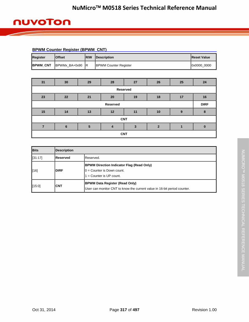
NuMicro M0518 Series Technical Reference Manual
Oct 31, 2014 Page 317 of 497 Revision 1.00
NU
MIC
RO
™ M
0518
SE
RIE
S T
EC
HN
ICA
L R
EF
ER
EN
CE
MA
NU
AL
BPWM Counter Register (BPWM_CNT)
Register Offset R/W Description Reset Value
BPWM_CNT BPWMx_BA+0x90 R BPWM Counter Register 0x0000_0000
31 30 29 28 27 26 25 24
Reserved
23 22 21 20 19 18 17 16
Reserved DIRF
15 14 13 12 11 10 9 8
CNT
7 6 5 4 3 2 1 0
CNT
Bits Description
[31:17] Reserved Reserved.
[16] DIRF
BPWM Direction Indicator Flag (Read Only)
0 = Counter is Down count.
1 = Counter is UP count.
[15:0] CNT BPWM Data Register (Read Only)
User can monitor CNT to know the current value in 16-bit period counter.

NuMicro M0518 Series Technical Reference Manual
Oct 31, 2014 Page 318 of 497 Revision 1.00
NU
MIC
RO
™ M
0518
SE
RIE
S T
EC
HN
ICA
L R
EF
ER
EN
CE
MA
NU
AL
BPWM Generation Register 0 (BPWM_WGCTL0)
Register Offset R/W Description Reset Value
BPWM_WGCTL0
BPWMx_BA+0xB0 R/W BPWM Generation Register 0 0x0000_0000
31 30 29 28 27 26 25 24
Reserved PRDPCTL5 PRDPCTL4
23 22 21 20 19 18 17 16
PRDPCTL3 PRDPCTL2 PRDPCTL1 PRDPCTL0
15 14 13 12 11 10 9 8
Reserved ZPCTL5 ZPCTL4
7 6 5 4 3 2 1 0
ZPCTL3 ZPCTL2 ZPCTL1 ZPCTL0
Bits Description
[31:28] Reserved Reserved.
[27:16] PRDPCTLn
BPWM Period (Center) Point Control
Each bit n controls the corresponding BPWM channel n.
00 = Do nothing.
01 = BPWM period (center) point output Low.
10 = BPWM period (center) point output High.
11 = BPWM period (center) point output Toggle.
BPWM can control output level when BPWM counter count to (PERIODn+1).
Note: This bit is center point control when BPWM counter operating in up-down counter type.
[15:12] Reserved Reserved.
[11:0] ZPCTLn
BPWM Zero Point Control
Each bit n controls the corresponding BPWM channel n.
00 = Do nothing.
01 = BPWM zero point output Low.
10 = BPWM zero point output High.
11 = BPWM zero point output Toggle.
BPWM can control output level when BPWM counter count to zero.

NuMicro M0518 Series Technical Reference Manual
Oct 31, 2014 Page 319 of 497 Revision 1.00
NU
MIC
RO
™ M
0518
SE
RIE
S T
EC
HN
ICA
L R
EF
ER
EN
CE
MA
NU
AL
BPWM Generation Register 1 (BPWM_WGCTL1)
Register Offset R/W Description Reset Value
BPWM_WGCTL1
BPWMx_BA+0xB4 R/W BPWM Generation Register 1 0x0000_0000
31 30 29 28 27 26 25 24
Reserved CMPDCTL5 CMPDCTL4
23 22 21 20 19 18 17 16
CMPDCTL3 CMPDCTL2 CMPDCTL1 CMPDCTL0
15 14 13 12 11 10 9 8
Reserved CMPUCTL5 CMPUCTL4
7 6 5 4 3 2 1 0
CMPUCTL3 CMPUCTL2 CMPUCTL1 CMPUCTL0
Bits Description
[31:28] Reserved Reserved.
[27:16] CMPDCTLn
BPWM Compare Down Point Control
Each bit n controls the corresponding BPWM channel n.
00 = Do nothing.
01 = BPWM compare down point output Low.
10 = BPWM compare down point output High.
11 = BPWM compare down point output Toggle.
BPWM can control output level when BPWM counter down count to CMPDAT.
Note: In complementary mode, CMPDCTL1, 3, 5 use as another CMPDCTL for channel 0, 2, 4.
[15:12] Reserved Reserved.
[11:0] CMPUCTLn
BPWM Compare Up Point Control
Each bit n controls the corresponding BPWM channel n.
00 = Do nothing.
01 = BPWM compare up point output Low.
10 = BPWM compare up point output High.
11 = BPWM compare up point output Toggle.
BPWM can control output level when BPWM counter up count to CMPDAT.
Note: In complementary mode, CMPUCTL1, 3, 5 use as another CMPUCTL for channel 0, 2, 4.
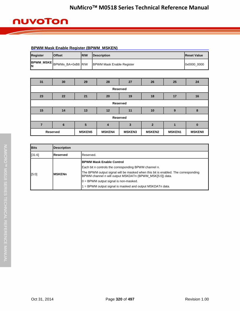
NuMicro M0518 Series Technical Reference Manual
Oct 31, 2014 Page 320 of 497 Revision 1.00
NU
MIC
RO
™ M
0518
SE
RIE
S T
EC
HN
ICA
L R
EF
ER
EN
CE
MA
NU
AL
BPWM Mask Enable Register (BPWM_MSKEN)
Register Offset R/W Description Reset Value
BPWM_MSKEN
BPWMx_BA+0xB8 R/W BPWM Mask Enable Register 0x0000_0000
31 30 29 28 27 26 25 24
Reserved
23 22 21 20 19 18 17 16
Reserved
15 14 13 12 11 10 9 8
Reserved
7 6 5 4 3 2 1 0
Reserved MSKEN5 MSKEN4 MSKEN3 MSKEN2 MSKEN1 MSKEN0
Bits Description
[31:6] Reserved Reserved.
[5:0] MSKENn
BPWM Mask Enable Control
Each bit n controls the corresponding BPWM channel n.
The BPWM output signal will be masked when this bit is enabled. The corresponding BPWM channel n will output MSKDATn (BPWM_MSK[5:0]) data.
0 = BPWM output signal is non-masked.
1 = BPWM output signal is masked and output MSKDATn data.
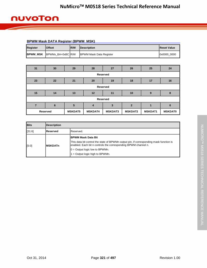
NuMicro M0518 Series Technical Reference Manual
Oct 31, 2014 Page 321 of 497 Revision 1.00
NU
MIC
RO
™ M
0518
SE
RIE
S T
EC
HN
ICA
L R
EF
ER
EN
CE
MA
NU
AL
BPWM Mask DATA Register (BPWM_MSK)
Register Offset R/W Description Reset Value
BPWM_MSK BPWMx_BA+0xBC R/W BPWM Mask Data Register 0x0000_0000
31 30 29 28 27 26 25 24
Reserved
23 22 21 20 19 18 17 16
Reserved
15 14 13 12 11 10 9 8
Reserved
7 6 5 4 3 2 1 0
Reserved MSKDAT5 MSKDAT4 MSKDAT3 MSKDAT2 MSKDAT1 MSKDAT0
Bits Description
[31:6] Reserved Reserved.
[5:0] MSKDATn
BPWM Mask Data Bit
This data bit control the state of BPWMn output pin, if corresponding mask function is enabled. Each bit n controls the corresponding BPWM channel n.
0 = Output logic low to BPWMn.
1 = Output logic high to BPWMn.

NuMicro M0518 Series Technical Reference Manual
Oct 31, 2014 Page 322 of 497 Revision 1.00
NU
MIC
RO
™ M
0518
SE
RIE
S T
EC
HN
ICA
L R
EF
ER
EN
CE
MA
NU
AL
BPWM Pin Polar Inverse Control (BPWM_POLCTL)
Register Offset R/W Description Reset Value
BPWM_POLCTL
BPWMx_BA+0xD4 R/W BPWM Pin Polar Inverse Register 0x0000_0000
31 30 29 28 27 26 25 24
Reserved
23 22 21 20 19 18 17 16
Reserved
15 14 13 12 11 10 9 8
Reserved
7 6 5 4 3 2 1 0
Reserved PINV5 PINV4 PINV3 PINV2 PINV1 PINV0
Bits Description
[31:6] Reserved Reserved.
[5:0] PINVn
BPWM PIN Polar Inverse Control
The register controls polarity state of BPWM output. Each bit n controls the corresponding BPWM channel n.
0 = BPWM output polar inverse Disabled.
1 = BPWM output polar inverse Enabled.
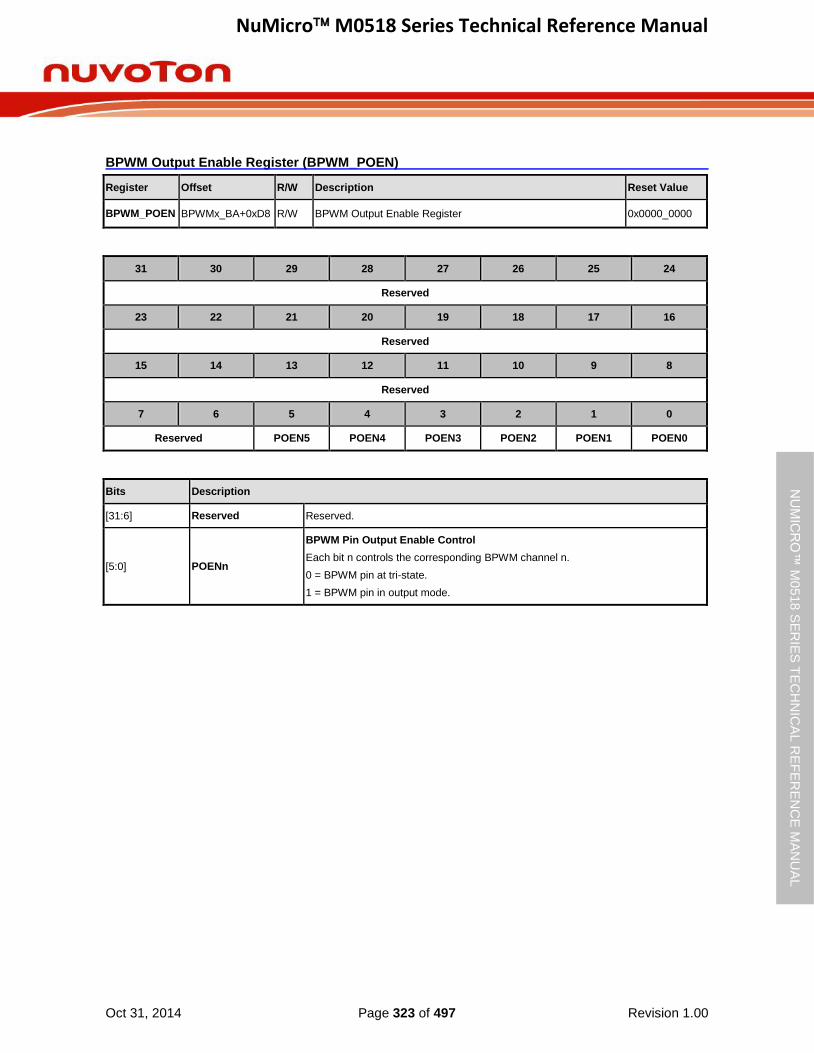
NuMicro M0518 Series Technical Reference Manual
Oct 31, 2014 Page 323 of 497 Revision 1.00
NU
MIC
RO
™ M
0518
SE
RIE
S T
EC
HN
ICA
L R
EF
ER
EN
CE
MA
NU
AL
BPWM Output Enable Register (BPWM_POEN)
Register Offset R/W Description Reset Value
BPWM_POEN BPWMx_BA+0xD8 R/W BPWM Output Enable Register 0x0000_0000
31 30 29 28 27 26 25 24
Reserved
23 22 21 20 19 18 17 16
Reserved
15 14 13 12 11 10 9 8
Reserved
7 6 5 4 3 2 1 0
Reserved POEN5 POEN4 POEN3 POEN2 POEN1 POEN0
Bits Description
[31:6] Reserved Reserved.
[5:0] POENn
BPWM Pin Output Enable Control
Each bit n controls the corresponding BPWM channel n.
0 = BPWM pin at tri-state.
1 = BPWM pin in output mode.

NuMicro M0518 Series Technical Reference Manual
Oct 31, 2014 Page 324 of 497 Revision 1.00
NU
MIC
RO
™ M
0518
SE
RIE
S T
EC
HN
ICA
L R
EF
ER
EN
CE
MA
NU
AL
BPWM Interrupt Enable Register (BPWM_INTEN)
Register Offset R/W Description Reset Value
BPWM_INTEN BPWMx_BA+0xE0 R/W BPWM Interrupt Enable Register 0x0000_0000
31 30 29 28 27 26 25 24
Reserved CMPDIEN5 CMPDIEN4 CMPDIEN3 CMPDIEN2 CMPDIEN1 CMPDIEN0
23 22 21 20 19 18 17 16
Reserved CMPUIEN5 CMPUIEN4 CMPUIEN3 CMPUIEN2 CMPUIEN1 CMPUIEN0
15 14 13 12 11 10 9 8
Reserved PIEN0
7 6 5 4 3 2 1 0
Reserved ZIEN0
Bits Description
[31:30] Reserved Reserved.
[29:24] CMPDIENn
BPWM Compare Down Count Interrupt Enable Control
Each bit n controls the corresponding BPWM channel n.
0 = Compare down count interrupt Disabled.
1 = Compare down count interrupt Enabled.
Note: In complementary mode, CMPDIEN1, 3, 5 use as another CMPDIEN for channel 0, 2, 4.
[23:22] Reserved Reserved.
[21:16] CMPUIENn
BPWM Compare Up Count Interrupt Enable Control
Each bit n controls the corresponding BPWM channel n.
0 = Compare up count interrupt Disabled.
1 = Compare up count interrupt Enabled.
Note: In complementary mode, CMPUIEN1, 3, 5 use as another CMPUIEN for channel 0, 2, 4.
[15:9] Reserved Reserved.
[8] PIEN0
BPWM Period Point Interrupt Enable 0
0 = Period point interrupt Disabled.
1 = Period point interrupt Enabled.
Note: When up-down counter type period point means center point.
[7:1] Reserved Reserved.
[0] ZIEN0
BPWM Zero Point Interrupt Enable 0
0 = Zero point interrupt Disabled.
1 = Zero point interrupt Enabled.
Note: Odd channels will read always 0 at complementary mode.

NuMicro M0518 Series Technical Reference Manual
Oct 31, 2014 Page 325 of 497 Revision 1.00
NU
MIC
RO
™ M
0518
SE
RIE
S T
EC
HN
ICA
L R
EF
ER
EN
CE
MA
NU
AL
BPWM Interrupt Flag Register (BPWM_INTSTS)
Register Offset R/W Description Reset Value
BPWM_INTSTS0
BPWMx_BA+0xE8 R/W BPWM Interrupt Flag Register 0 0x0000_0000
31 30 29 28 27 26 25 24
Reserved CMPDIF5 CMPDIF4 CMPDIF3 CMPDIF2 CMPDIF1 CMPDIF0
23 22 21 20 19 18 17 16
Reserved CMPUIF5 CMPUIF4 CMPUIF3 CMPUIF2 CMPUIF1 CMPUIF0
15 14 13 12 11 10 9 8
Reserved PIF0
7 6 5 4 3 2 1 0
Reserved ZIF0
Bits Description
[31:30] Reserved Reserved.
[29:24] CMPDIFn
BPWM Compare Down Count Interrupt Flag
Each bit n controls the corresponding BPWM channel n.
Flag is set by hardware when BPWM counter down count and reaches BPWM_CMPDATn, software can clear this bit by writing 1 to it.
Note1: If CMPDAT equal to PERIOD, this flag is not working in down counter type selection.
Note2: In complementary mode, CMPDIF1, 3, 5 use as another CMPDIF for channel 0, 2, 4.
[23:22] Reserved Reserved.
[21:16] CMPUIFn
BPWM Compare Up Count Interrupt Flag
Flag is set by hardware when BPWM counter up count and reaches BPWM_CMPDATn, software can clear this bit by writing 1 to it. Each bit n controls the corresponding BPWM channel n.
Note1: If CMPDAT equal to PERIOD, this flag is not working in up counter type selection.
Note2: In complementary mode, CMPUIF1, 3, 5 use as another CMPUIF for channel 0, 2, 4.
[15:9] Reserved Reserved.
[8] PIF0
BPWM Period Point Interrupt Flag 0
This bit is set by hardware when BPWM_CH0 counter reaches BPWM_PERIOD0, software can write 1 to clear this bit to zero.
[7:1] Reserved Reserved.
[0] ZIF0
BPWM Zero Point Interrupt Flag 0
This bit is set by hardware when BPWM_CH0 counter reaches zero, software can write 1 to clear this bit to zero.

NuMicro M0518 Series Technical Reference Manual
Oct 31, 2014 Page 326 of 497 Revision 1.00
NU
MIC
RO
™ M
0518
SE
RIE
S T
EC
HN
ICA
L R
EF
ER
EN
CE
MA
NU
AL
BPWM Trigger ADC Source Select Register 0 (BPWM_ADCTS0)
Register Offset R/W Description Reset Value
BPWM_ADCTS0
BPWMx_BA+0xF8 R/W BPWM Trigger ADC Source Select Register 0 0x0000_0000
31 30 29 28 27 26 25 24
TRGEN3 Reserved TRGSEL3
23 22 21 20 19 18 17 16
TRGEN2 Reserved TRGSEL2
15 14 13 12 11 10 9 8
TRGEN1 Reserved TRGSEL1
7 6 5 4 3 2 1 0
TRGEN0 Reserved TRGSEL0
Bits Description
[31] TRGEN3 BPWM_CH3 Trigger ADC Enable Bit
[30:28] Reserved Reserved.
[27:24] TRGSEL3
BPWM_CH3 Trigger ADC Source Select
0000 = BPWM_CH2 zero point.
0001 = BPWM_CH2 period point.
0010 = BPWM_CH2 zero or period point.
0011 = BPWM_CH2 up-count CMPDAT point.
0100 = BPWM_CH2 down-count CMPDAT point.
0101 = Reserved.
0110 = Reserved.
0111 = Reserved.
1000 = BPWM_CH3 up-count CMPDAT point.
1001 = BPWM_CH3 down-count CMPDAT point.
Others = reserved.
[23] TRGEN2 BPWM_CH2 Trigger ADC Enable Bit
[22:20] Reserved Reserved.
[19:16] TRGSEL2
BPWM_CH2 Trigger ADC Source Select
0000 = BPWM_CH2 zero point.
0001 = BPWM_CH2 period point.
0010 = BPWM_CH2 zero or period point.
0011 = BPWM_CH2 up-count CMPDAT point.
0100 = BPWM_CH2 down-count CMPDAT point.
0101 = Reserved.
0110 = Reserved.
0111 = Reserved.

NuMicro M0518 Series Technical Reference Manual
Oct 31, 2014 Page 327 of 497 Revision 1.00
NU
MIC
RO
™ M
0518
SE
RIE
S T
EC
HN
ICA
L R
EF
ER
EN
CE
MA
NU
AL
1000 = BPWM_CH3 up-count CMPDAT point.
1001 = BPWM_CH3 down-count CMPDAT point.
Others reserved.
[15] TRGEN1 BPWM_CH1 Trigger ADC Enable Bit
[14:12] Reserved Reserved.
[11:8] TRGSEL1
BPWM_CH1 Trigger ADC Source Select
0000 = BPWM_CH0 zero point.
0001 = BPWM_CH0 period point.
0010 = BPWM_CH0 zero or period point.
0011 = BPWM_CH0 up-count CMPDAT point.
0100 = BPWM_CH0 down-count CMPDAT point.
0101 = Reserved.
0110 = Reserved.
0111 = Reserved.
1000 = BPWM_CH1 up-count CMPDAT point.
1001 = BPWM_CH1 down-count CMPDAT point.
Others = reserved.
[7] TRGEN0 BPWM_CH0 Trigger ADC Enable Bit
[6:4] Reserved Reserved.
[3:0] TRGSEL0
BPWM_CH0 Trigger ADC Source Select
0000 = BPWM_CH0 zero point.
0001 = BPWM_CH0 period point.
0010 = BPWM_CH0 zero or period point.
0011 = BPWM_CH0 up-count CMPDAT point.
0100 = BPWM_CH0 down-count CMPDAT point.
0101 = Reserved.
0110 = Reserved.
0111 = Reserved.
1000 = BPWM_CH1 up-count CMPDAT point.
1001 = BPWM_CH1 down-count CMPDAT point.
Others = reserved.

NuMicro M0518 Series Technical Reference Manual
Oct 31, 2014 Page 328 of 497 Revision 1.00
NU
MIC
RO
™ M
0518
SE
RIE
S T
EC
HN
ICA
L R
EF
ER
EN
CE
MA
NU
AL
BPWM Trigger ADC Source Select Register 1 (BPWM_ADCTS1)
Register Offset R/W Description Reset Value
BPWM_ADCTS1
BPWMx_BA+0xFC R/W BPWM Trigger ADC Source Select Register 1 0x0000_0000
31 30 29 28 27 26 25 24
Reserved
23 22 21 20 19 18 17 16
Reserved
15 14 13 12 11 10 9 8
TRGEN5 Reserved TRGSEL5
7 6 5 4 3 2 1 0
TRGEN4 Reserved TRGSEL4
Bits Description
[31:16] Reserved Reserved.
[15] TRGEN5 BPWM_CH5 Trigger ADC Enable Bit
[14:12] Reserved Reserved.
[11:8] TRGSEL5
BPWM_CH5 Trigger ADC Source Select
0000 = BPWM_CH4 zero point.
0001 = BPWM_CH4 period point.
0010 = BPWM_CH4 zero or period point.
0011 = BPWM_CH4 up-count CMPDAT point.
0100 = BPWM_CH4 down-count CMPDAT point.
0101 = Reserved.
0110 = Reserved.
0111 = Reserved.
1000 = BPWM_CH5 up-count CMPDAT point.
1001 = BPWM_CH5 down-count CMPDAT point.
Others = reserved.
[7] TRGEN4 BPWM_CH4 Trigger ADC Enable Bit
[6:4] Reserved Reserved.
[3:0] TRGSEL4
BPWM_CH4 Trigger ADC Source Select
0000 = BPWM_CH4 zero point.
0001 = BPWM_CH4 period point.
0010 = BPWM_CH4 zero or period point.
0011 = BPWM_CH4 up-count CMPDAT point.
0100 = BPWM_CH4 down-count CMPDAT point.
0101 = Reserved.

NuMicro M0518 Series Technical Reference Manual
Oct 31, 2014 Page 329 of 497 Revision 1.00
NU
MIC
RO
™ M
0518
SE
RIE
S T
EC
HN
ICA
L R
EF
ER
EN
CE
MA
NU
AL
0110 = Reserved.
0111 = Reserved.
1000 = BPWM_CH5 up-count CMPDAT point.
1001 = BPWM_CH5 down-count CMPDAT point.
Others = reserved.
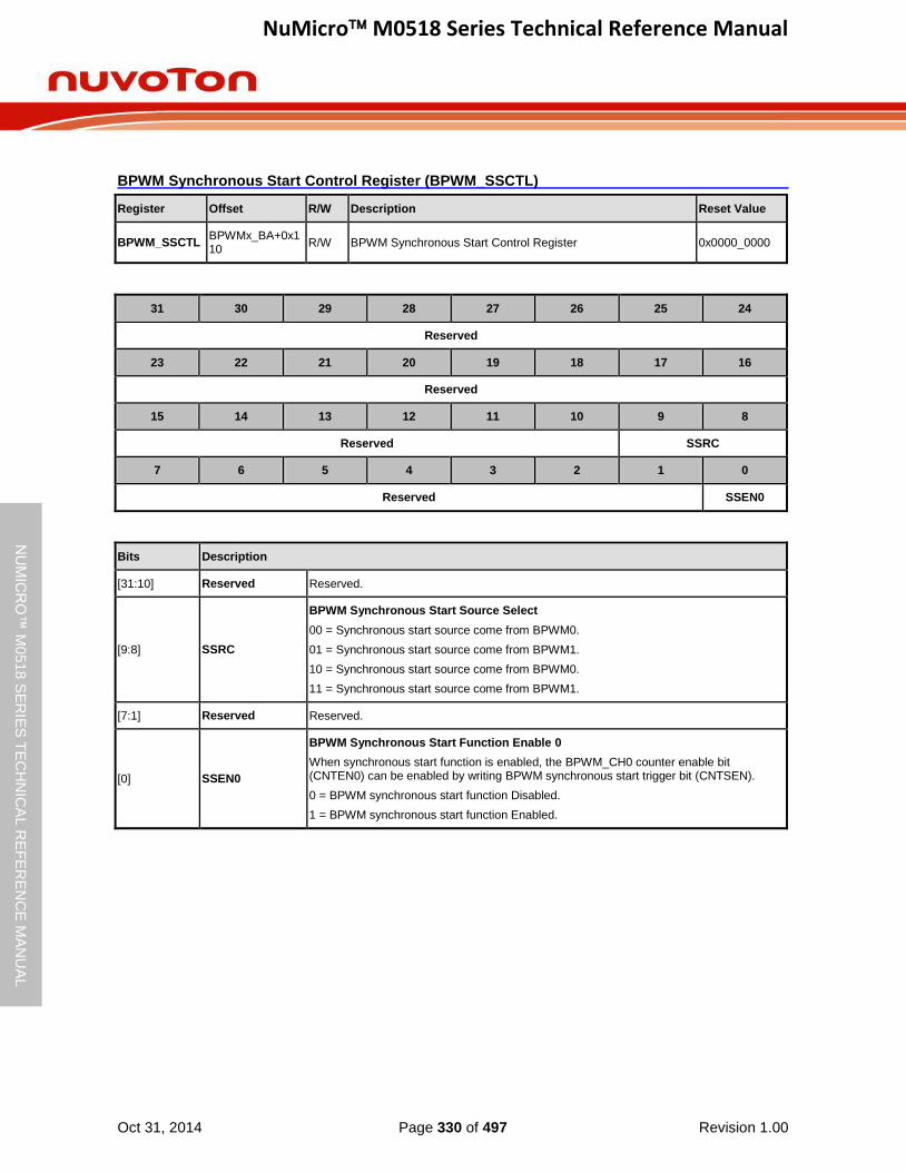
NuMicro M0518 Series Technical Reference Manual
Oct 31, 2014 Page 330 of 497 Revision 1.00
NU
MIC
RO
™ M
0518
SE
RIE
S T
EC
HN
ICA
L R
EF
ER
EN
CE
MA
NU
AL
BPWM Synchronous Start Control Register (BPWM_SSCTL)
Register Offset R/W Description Reset Value
BPWM_SSCTL BPWMx_BA+0x110
R/W BPWM Synchronous Start Control Register 0x0000_0000
31 30 29 28 27 26 25 24
Reserved
23 22 21 20 19 18 17 16
Reserved
15 14 13 12 11 10 9 8
Reserved SSRC
7 6 5 4 3 2 1 0
Reserved SSEN0
Bits Description
[31:10] Reserved Reserved.
[9:8] SSRC
BPWM Synchronous Start Source Select
00 = Synchronous start source come from BPWM0.
01 = Synchronous start source come from BPWM1.
10 = Synchronous start source come from BPWM0.
11 = Synchronous start source come from BPWM1.
[7:1] Reserved Reserved.
[0] SSEN0
BPWM Synchronous Start Function Enable 0
When synchronous start function is enabled, the BPWM_CH0 counter enable bit (CNTEN0) can be enabled by writing BPWM synchronous start trigger bit (CNTSEN).
0 = BPWM synchronous start function Disabled.
1 = BPWM synchronous start function Enabled.
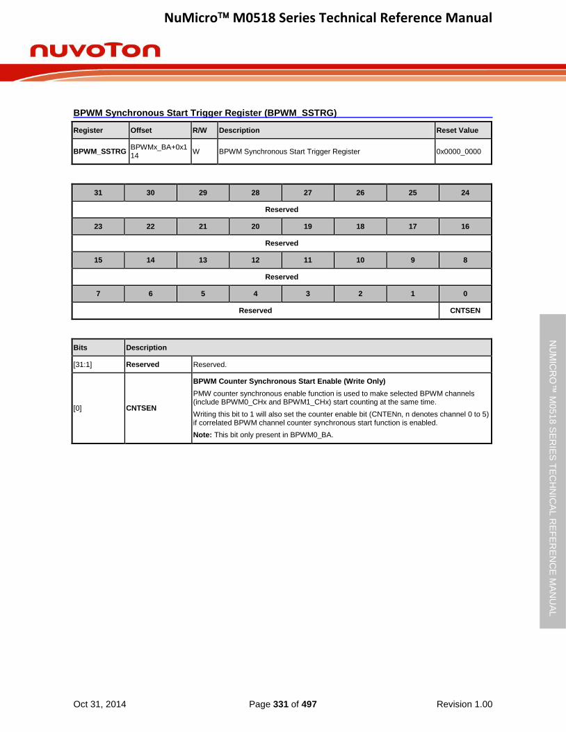
NuMicro M0518 Series Technical Reference Manual
Oct 31, 2014 Page 331 of 497 Revision 1.00
NU
MIC
RO
™ M
0518
SE
RIE
S T
EC
HN
ICA
L R
EF
ER
EN
CE
MA
NU
AL
BPWM Synchronous Start Trigger Register (BPWM_SSTRG)
Register Offset R/W Description Reset Value
BPWM_SSTRG BPWMx_BA+0x114
W BPWM Synchronous Start Trigger Register 0x0000_0000
31 30 29 28 27 26 25 24
Reserved
23 22 21 20 19 18 17 16
Reserved
15 14 13 12 11 10 9 8
Reserved
7 6 5 4 3 2 1 0
Reserved CNTSEN
Bits Description
[31:1] Reserved Reserved.
[0] CNTSEN
BPWM Counter Synchronous Start Enable (Write Only)
PMW counter synchronous enable function is used to make selected BPWM channels (include BPWM0_CHx and BPWM1_CHx) start counting at the same time.
Writing this bit to 1 will also set the counter enable bit (CNTENn, n denotes channel 0 to 5) if correlated BPWM channel counter synchronous start function is enabled.
Note: This bit only present in BPWM0_BA.

NuMicro M0518 Series Technical Reference Manual
Oct 31, 2014 Page 332 of 497 Revision 1.00
NU
MIC
RO
™ M
0518
SE
RIE
S T
EC
HN
ICA
L R
EF
ER
EN
CE
MA
NU
AL
BPWM Status Register (BPWM_STATUS)
Register Offset R/W Description Reset Value
BPWM_STATUS
BPWMx_BA+0x120
R/W BPWM Status Register 0x0000_0000
31 30 29 28 27 26 25 24
Reserved
23 22 21 20 19 18 17 16
Reserved ADCTRG5 ADCTRG4 ADCTRG3 ADCTRG2 ADCTRG1 ADCTRG0
15 14 13 12 11 10 9 8
Reserved
7 6 5 4 3 2 1 0
Reserved CNTMAX0
Bits Description
[31:22] Reserved Reserved.
[21:16] ADCTRGn
ADC Start Of Conversion Status
Each bit n controls the corresponding BPWM channel n.
0 = Indicates no ADC start of conversion trigger event has occurred.
1 = Indicates an ADC start of conversion trigger event has occurred, software can write 1 to clear this bit.
[15:1] Reserved Reserved.
[0] CNTMAX0
Time-Base Counter 0 Equal To 0xFFFF Latched Status
0 = Indicates the time-base counter never reached its maximum value 0xFFFF.
1 = Indicates the time-base counter reached its maximum value, software can write 1 to clear this bit.

NuMicro M0518 Series Technical Reference Manual
Oct 31, 2014 Page 333 of 497 Revision 1.00
NU
MIC
RO
™ M
0518
SE
RIE
S T
EC
HN
ICA
L R
EF
ER
EN
CE
MA
NU
AL
BPWM Capture Input Enable Register (BPWM_CAPINEN)
Register Offset R/W Description Reset Value
BPWM_CAPINEN
BPWMx_BA+0x200
R/W BPWM Capture Input Enable Register 0x0000_0000
31 30 29 28 27 26 25 24
Reserved
23 22 21 20 19 18 17 16
Reserved
15 14 13 12 11 10 9 8
Reserved
7 6 5 4 3 2 1 0
Reserved CAPINEN5 CAPINEN4 CAPINEN3 CAPINEN2 CAPINEN1 CAPINEN0
Bits Description
[31:6] Reserved Reserved.
[5:0] CAPINENn
Capture Input Enable Control
Each bit n controls the corresponding BPWM channel n.
0 = BPWM Channel capture input path Disabled. The input of BPWM channel capture function is always regarded as 0.
1 = BPWM Channel capture input path Enabled. The input of BPWM channel capture function comes from correlative multifunction pin.
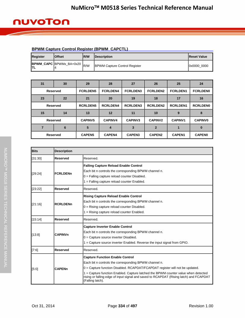
NuMicro M0518 Series Technical Reference Manual
Oct 31, 2014 Page 334 of 497 Revision 1.00
NU
MIC
RO
™ M
0518
SE
RIE
S T
EC
HN
ICA
L R
EF
ER
EN
CE
MA
NU
AL
BPWM Capture Control Register (BPWM_CAPCTL)
Register Offset R/W Description Reset Value
BPWM_CAPCTL
BPWMx_BA+0x204
R/W BPWM Capture Control Register 0x0000_0000
31 30 29 28 27 26 25 24
Reserved FCRLDEN5 FCRLDEN4 FCRLDEN3 FCRLDEN2 FCRLDEN1 FCRLDEN0
23 22 21 20 19 18 17 16
Reserved RCRLDEN5 RCRLDEN4 RCRLDEN3 RCRLDEN2 RCRLDEN1 RCRLDEN0
15 14 13 12 11 10 9 8
Reserved CAPINV5 CAPINV4 CAPINV3 CAPINV2 CAPINV1 CAPINV0
7 6 5 4 3 2 1 0
Reserved CAPEN5 CAPEN4 CAPEN3 CAPEN2 CAPEN1 CAPEN0
Bits Description
[31:30] Reserved Reserved.
[29:24] FCRLDENn
Falling Capture Reload Enable Control
Each bit n controls the corresponding BPWM channel n.
0 = Falling capture reload counter Disabled.
1 = Falling capture reload counter Enabled.
[23:22] Reserved Reserved.
[21:16] RCRLDENn
Rising Capture Reload Enable Control
Each bit n controls the corresponding BPWM channel n.
0 = Rising capture reload counter Disabled.
1 = Rising capture reload counter Enabled.
[15:14] Reserved Reserved.
[13:8] CAPINVn
Capture Inverter Enable Control
Each bit n controls the corresponding BPWM channel n.
0 = Capture source inverter Disabled.
1 = Capture source inverter Enabled. Reverse the input signal from GPIO.
[7:6] Reserved Reserved.
[5:0] CAPENn
Capture Function Enable Control
Each bit n controls the corresponding BPWM channel n.
0 = Capture function Disabled. RCAPDAT/FCAPDAT register will not be updated.
1 = Capture function Enabled. Capture latched the BPWM counter value when detected rising or falling edge of input signal and saved to RCAPDAT (Rising latch) and FCAPDAT (Falling latch).

NuMicro M0518 Series Technical Reference Manual
Oct 31, 2014 Page 335 of 497 Revision 1.00
NU
MIC
RO
™ M
0518
SE
RIE
S T
EC
HN
ICA
L R
EF
ER
EN
CE
MA
NU
AL
BPWM Capture Status Register (BPWM_CAPSTS)
Register Offset R/W Description Reset Value
BPWM_CAPSTS
BPWMx_BA+0x208
R BPWM Capture Status Register 0x0000_0000
31 30 29 28 27 26 25 24
Reserved
23 22 21 20 19 18 17 16
Reserved
15 14 13 12 11 10 9 8
Reserved CFLIFOV5 CFLIFOV4 CFLIFOV3 CFLIFOV2 CFLIFOV1 CFLIFOV0
7 6 5 4 3 2 1 0
Reserved CRLIFOV5 CRLIFOV4 CRLIFOV3 CRLIFOV2 CRLIFOV1 CRLIFOV0
Bits Description
[31:14] Reserved Reserved.
[13:8] CFLIFOVn
Capture Falling Latch Interrupt Flag Overrun Status (Read Only)
This flag indicates if falling latch happened when the corresponding CFLIF is 1. Each bit n controls the corresponding BPWM channel n.
Note: This bit will be cleared automatically when user clear corresponding CFLIF.
[7:6] Reserved Reserved.
[5:0] CRLIFOVn
Capture Rising Latch Interrupt Flag Overrun Status (Read Only)
This flag indicates if rising latch happened when the corresponding CRLIF is 1. Each bit n controls the corresponding BPWM channel n.
Note: This bit will be cleared automatically when user clear corresponding CRLIF.
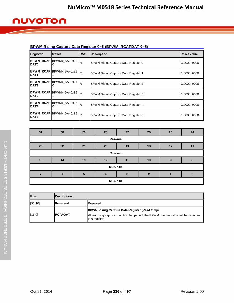
NuMicro M0518 Series Technical Reference Manual
Oct 31, 2014 Page 336 of 497 Revision 1.00
NU
MIC
RO
™ M
0518
SE
RIE
S T
EC
HN
ICA
L R
EF
ER
EN
CE
MA
NU
AL
BPWM Rising Capture Data Register 0~5 (BPWM_RCAPDAT 0~5)
Register Offset R/W Description Reset Value
BPWM_RCAPDAT0
BPWMx_BA+0x20C
R BPWM Rising Capture Data Register 0 0x0000_0000
BPWM_RCAPDAT1
BPWMx_BA+0x214
R BPWM Rising Capture Data Register 1 0x0000_0000
BPWM_RCAPDAT2
BPWMx_BA+0x21C
R BPWM Rising Capture Data Register 2 0x0000_0000
BPWM_RCAPDAT3
BPWMx_BA+0x224
R BPWM Rising Capture Data Register 3 0x0000_0000
BPWM_RCAPDAT4
BPWMx_BA+0x22C
R BPWM Rising Capture Data Register 4 0x0000_0000
BPWM_RCAPDAT5
BPWMx_BA+0x234
R BPWM Rising Capture Data Register 5 0x0000_0000
31 30 29 28 27 26 25 24
Reserved
23 22 21 20 19 18 17 16
Reserved
15 14 13 12 11 10 9 8
RCAPDAT
7 6 5 4 3 2 1 0
RCAPDAT
Bits Description
[31:16] Reserved Reserved.
[15:0] RCAPDAT
BPWM Rising Capture Data Register (Read Only)
When rising capture condition happened, the BPWM counter value will be saved in this register.
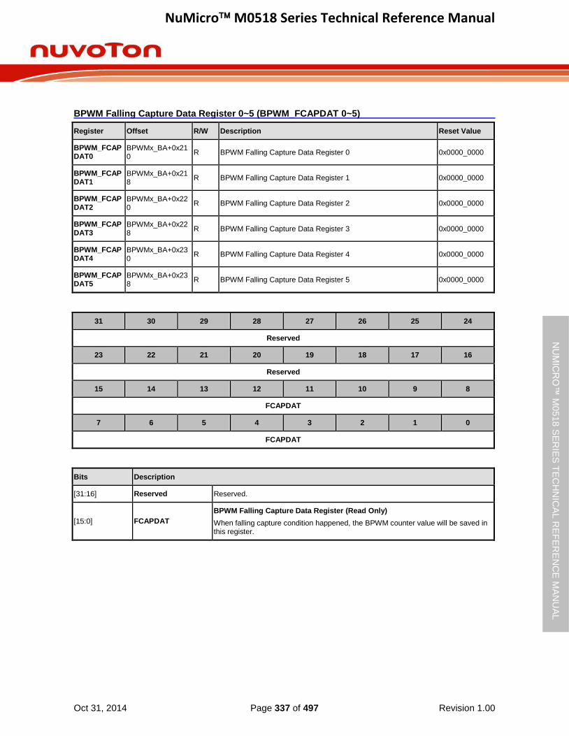
NuMicro M0518 Series Technical Reference Manual
Oct 31, 2014 Page 337 of 497 Revision 1.00
NU
MIC
RO
™ M
0518
SE
RIE
S T
EC
HN
ICA
L R
EF
ER
EN
CE
MA
NU
AL
BPWM Falling Capture Data Register 0~5 (BPWM_FCAPDAT 0~5)
Register Offset R/W Description Reset Value
BPWM_FCAPDAT0
BPWMx_BA+0x210
R BPWM Falling Capture Data Register 0 0x0000_0000
BPWM_FCAPDAT1
BPWMx_BA+0x218
R BPWM Falling Capture Data Register 1 0x0000_0000
BPWM_FCAPDAT2
BPWMx_BA+0x220
R BPWM Falling Capture Data Register 2 0x0000_0000
BPWM_FCAPDAT3
BPWMx_BA+0x228
R BPWM Falling Capture Data Register 3 0x0000_0000
BPWM_FCAPDAT4
BPWMx_BA+0x230
R BPWM Falling Capture Data Register 4 0x0000_0000
BPWM_FCAPDAT5
BPWMx_BA+0x238
R BPWM Falling Capture Data Register 5 0x0000_0000
31 30 29 28 27 26 25 24
Reserved
23 22 21 20 19 18 17 16
Reserved
15 14 13 12 11 10 9 8
FCAPDAT
7 6 5 4 3 2 1 0
FCAPDAT
Bits Description
[31:16] Reserved Reserved.
[15:0] FCAPDAT
BPWM Falling Capture Data Register (Read Only)
When falling capture condition happened, the BPWM counter value will be saved in this register.
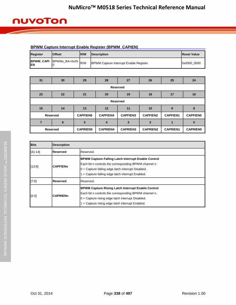
NuMicro M0518 Series Technical Reference Manual
Oct 31, 2014 Page 338 of 497 Revision 1.00
NU
MIC
RO
™ M
0518
SE
RIE
S T
EC
HN
ICA
L R
EF
ER
EN
CE
MA
NU
AL
BPWM Capture Interrupt Enable Register (BPWM_CAPIEN)
Register Offset R/W Description Reset Value
BPWM_CAPIEN
BPWMx_BA+0x250
R/W BPWM Capture Interrupt Enable Register 0x0000_0000
31 30 29 28 27 26 25 24
Reserved
23 22 21 20 19 18 17 16
Reserved
15 14 13 12 11 10 9 8
Reserved CAPFIEN5 CAPFIEN4 CAPFIEN3 CAPFIEN2 CAPFIEN1 CAPFIEN0
7 6 5 4 3 2 1 0
Reserved CAPRIEN5 CAPRIEN4 CAPRIEN3 CAPRIEN2 CAPRIEN1 CAPRIEN0
Bits Description
[31:14] Reserved Reserved.
[13:8] CAPFIENn
BPWM Capture Falling Latch Interrupt Enable Control
Each bit n controls the corresponding BPWM channel n.
0 = Capture falling edge latch interrupt Disabled.
1 = Capture falling edge latch interrupt Enabled.
[7:6] Reserved Reserved.
[5:0] CAPRIENn
BPWM Capture Rising Latch Interrupt Enable Control
Each bit n controls the corresponding BPWM channel n.
0 = Capture rising edge latch interrupt Disabled.
1 = Capture rising edge latch interrupt Enabled.

NuMicro M0518 Series Technical Reference Manual
Oct 31, 2014 Page 339 of 497 Revision 1.00
NU
MIC
RO
™ M
0518
SE
RIE
S T
EC
HN
ICA
L R
EF
ER
EN
CE
MA
NU
AL
BPWM Capture Interrupt Flag Register (BPWM_CAPIF)
Register Offset R/W Description Reset Value
BPWM_CAPIF BPWMx_BA+0x254
R/W BPWM Capture Interrupt Flag Register 0x0000_0000
31 30 29 28 27 26 25 24
Reserved
23 22 21 20 19 18 17 16
Reserved
15 14 13 12 11 10 9 8
Reserved CFLIF5 CFLIF4 CFLIF3 CFLIF2 CFLIF1 CFLIF0
7 6 5 4 3 2 1 0
Reserved CRLIF5 CRLIF4 CRLIF3 CRLIF2 CRLIF1 CRLIF0
Bits Description
[31:14] Reserved Reserved.
[13:8] CFLIFn
BPWM Capture Falling Latch Interrupt Flag
This bit is writing 1 to clear. Each bit n controls the corresponding BPWM channel n.
0 = No capture falling latch condition happened.
1 = Capture falling latch condition happened, this flag will be set to high.
[7:6] Reserved Reserved.
[5:0] CRLIFn
BPWM Capture Rising Latch Interrupt Flag
This bit is writing 1 to clear. Each bit n controls the corresponding BPWM channel n.
0 = No capture rising latch condition happened.
1 = Capture rising latch condition happened, this flag will be set to high.

NuMicro M0518 Series Technical Reference Manual
Oct 31, 2014 Page 340 of 497 Revision 1.00
NU
MIC
RO
™ M
0518
SE
RIE
S T
EC
HN
ICA
L R
EF
ER
EN
CE
MA
NU
AL
BPWM Period Register Buffer (BPWM_PBUF)
Register Offset R/W Description Reset Value
BPWM_PBUF BPWMx_BA+0x304
R BPWM PERIOD Buffer 0x0000_0000
31 30 29 28 27 26 25 24
Reserved
23 22 21 20 19 18 17 16
Reserved
15 14 13 12 11 10 9 8
PBUF
7 6 5 4 3 2 1 0
PBUF
Bits Description
[31:16] Reserved Reserved.
[15:0] PBUF BPWM Period Register Buffer (Read Only)
Used as PERIOD active register.
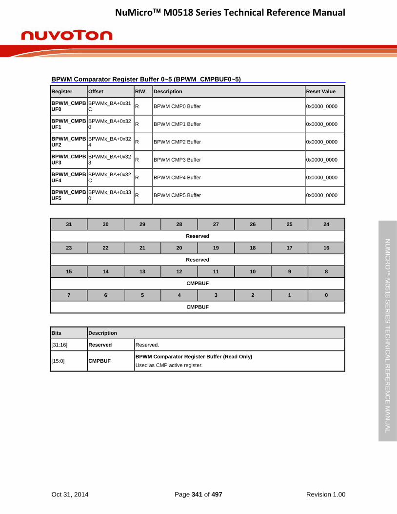
NuMicro M0518 Series Technical Reference Manual
Oct 31, 2014 Page 341 of 497 Revision 1.00
NU
MIC
RO
™ M
0518
SE
RIE
S T
EC
HN
ICA
L R
EF
ER
EN
CE
MA
NU
AL
BPWM Comparator Register Buffer 0~5 (BPWM_CMPBUF0~5)
Register Offset R/W Description Reset Value
BPWM_CMPBUF0
BPWMx_BA+0x31C
R BPWM CMP0 Buffer 0x0000_0000
BPWM_CMPBUF1
BPWMx_BA+0x320
R BPWM CMP1 Buffer 0x0000_0000
BPWM_CMPBUF2
BPWMx_BA+0x324
R BPWM CMP2 Buffer 0x0000_0000
BPWM_CMPBUF3
BPWMx_BA+0x328
R BPWM CMP3 Buffer 0x0000_0000
BPWM_CMPBUF4
BPWMx_BA+0x32C
R BPWM CMP4 Buffer 0x0000_0000
BPWM_CMPBUF5
BPWMx_BA+0x330
R BPWM CMP5 Buffer 0x0000_0000
31 30 29 28 27 26 25 24
Reserved
23 22 21 20 19 18 17 16
Reserved
15 14 13 12 11 10 9 8
CMPBUF
7 6 5 4 3 2 1 0
CMPBUF
Bits Description
[31:16] Reserved Reserved.
[15:0] CMPBUF BPWM Comparator Register Buffer (Read Only)
Used as CMP active register.
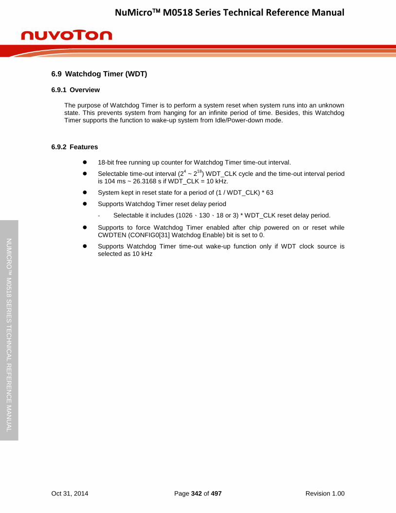
NuMicro M0518 Series Technical Reference Manual
Oct 31, 2014 Page 342 of 497 Revision 1.00
NU
MIC
RO
™ M
0518
SE
RIE
S T
EC
HN
ICA
L R
EF
ER
EN
CE
MA
NU
AL
6.9 Watchdog Timer (WDT)
6.9.1 Overview
The purpose of Watchdog Timer is to perform a system reset when system runs into an unknown state. This prevents system from hanging for an infinite period of time. Besides, this Watchdog Timer supports the function to wake-up system from Idle/Power-down mode.
6.9.2 Features
18-bit free running up counter for Watchdog Timer time-out interval.
Selectable time-out interval (24 ~ 2
18) WDT_CLK cycle and the time-out interval period
is 104 ms ~ 26.3168 s if WDT_CLK = 10 kHz.
System kept in reset state for a period of (1 / WDT_CLK) * 63
Supports Watchdog Timer reset delay period
- Selectable it includes (1026、130、18 or 3) * WDT_CLK reset delay period.
Supports to force Watchdog Timer enabled after chip powered on or reset while CWDTEN (CONFIG0[31] Watchdog Enable) bit is set to 0.
Supports Watchdog Timer time-out wake-up function only if WDT clock source is selected as 10 kHz
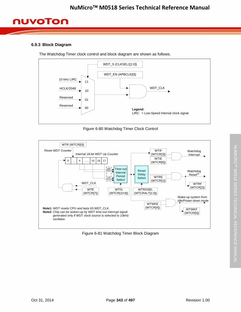
NuMicro M0518 Series Technical Reference Manual
Oct 31, 2014 Page 343 of 497 Revision 1.00
NU
MIC
RO
™ M
0518
SE
RIE
S T
EC
HN
ICA
L R
EF
ER
EN
CE
MA
NU
AL
6.9.3 Block Diagram
The Watchdog Timer clock control and block diagram are shown as follows.
10
01
HCLK/2048
10 kHz LIRC
WDT_S (CLKSEL1[1:0])
WDT_EN (APBCLK[0])
WDT_CLK
11
Reserved
Legend:
LIRC = Low-Speed Internal clock signal
00Reserved
Figure 6-80 Watchdog Timer Clock Control
Internal 18-bit WDT Up Counter
0 …... 15.. 4 16 17
000001
110111
:
:
WDT_CLK
Time-out
Interval
Period
Select
Reset
Delay
Select
Watchdog
Interrupt
WTRE
(WTCR[1])
Watchdog
Reset[1]
WTR (WTCR[0])
Reset WDT Counter
Note1: WDT resets CPU and lasts 63 WDT_CLK.
Note2: Chip can be woken-up by WDT time-out interrupt signal
generated only if WDT clock source is selected to 10kHz
oscillator.
WTIE
(WTCR[6])
WTE
(WTCR[7])
WTIF
(WTCR[3])
WTRF
(WTCR[2])WTIS
(WTCR[10:8])
Wake-up system from
Idle/Power-down modeWTWKE
(WTCR[4])WTWKF
(WTCR[5])
WTRDSEL
(WTCRALT[1:0])
Figure 6-81 Watchdog Timer Block Diagram
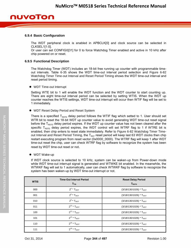
NuMicro M0518 Series Technical Reference Manual
Oct 31, 2014 Page 344 of 497 Revision 1.00
NU
MIC
RO
™ M
0518
SE
RIE
S T
EC
HN
ICA
L R
EF
ER
EN
CE
MA
NU
AL
6.9.4 Basic Configuration
The WDT peripheral clock is enabled in APBCLK[0] and clock source can be selected in CLKSEL1[1:0]. Or user can set CONFIG0[31] for 0 to force Watchdog Timer enabled and active in 10 kHz after chip powered on or reset.
6.9.5 Functional Description
The Watchdog Timer (WDT) includes an 18-bit free running up counter with programmable time-out intervals. Table 6-35 shows the WDT time-out interval period selection and Figure 6-82 Watchdog Timer Time-out Interval and Reset Period Timing shows the WDT time-out interval and reset period timing.
WDT Time-out Interrupt
Setting WTE bit to 1 will enable the WDT function and the WDT counter to start counting up. There are eight time-out interval period can be selected by setting WTIS. When the WDT up counter reaches the WTIS settings, WDT time-out interrupt will occur then WTIF flag will be set to 1 immediately.
WDT Reset Delay Period and Reset System
There is a specified TRSTD delay period follows the WTIF flag which setted to 1. User should set
WTR bit to reset the 18-bit WDT up counter value to avoid generating WDT time-out reset signal before the TRSTD delay period expires. If the WDT up counter value has not been cleared after the
specific TRSTD delay period expires, the WDT control will set WTRF flag to 1 if WTRE bit is
enabled, then chip enters to reset state immediately. Refer to Figure 6-82 Watchdog Timer Time-out Interval and Reset Period Timing, the TRST reset period will keep last 63 WDT clocks then chip
restart executing program from reset vector (0x0000_0000). The WTRF flag will keep 1 after WDT time-out reset the chip, user can check WTRF flag by software to recognize the system has been
reset by WDT time-out reset or not.
WDT Wake-up
If WDT clock source is selected to 10 kHz, system can be waken-up from Power-down mode while WDT time-out interrupt signal is generated and WTWKE bit enabled. In the meanwhile, the WTWKF flag will set to 1 automatically, user can check WTWKF flag by software to recognize the system has been waken-up by WDT time-out interrupt or not.
WTIS Time-Out Interval Period
TTIS
Reset Delay Period
TRSTD
000 24 * TWDT (3/18/130/1026) * TWDT
001 26 * TWDT (3/18/130/1026) * TWDT
010 28 * TWDT (3/18/130/1026) * TWDT
011 210
* TWDT (3/18/130/1026) * TWDT
100 212
* TWDT (3/18/130/1026) * TWDT
101 214
* TWDT (3/18/130/1026) * TWDT
110 216
* TWDT (3/18/130/1026) * TWDT
111 218
* TWDT (3/18/130/1026) * TWDT
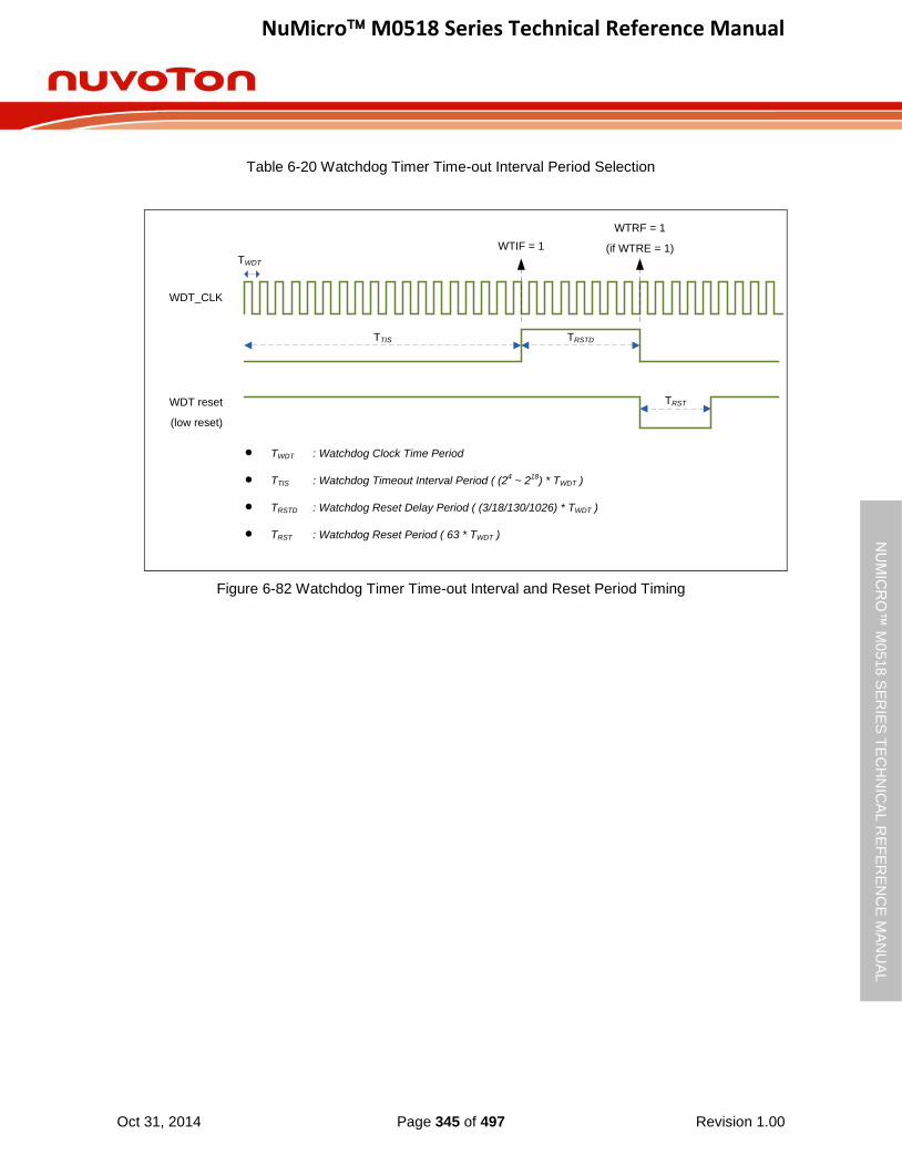
NuMicro M0518 Series Technical Reference Manual
Oct 31, 2014 Page 345 of 497 Revision 1.00
NU
MIC
RO
™ M
0518
SE
RIE
S T
EC
HN
ICA
L R
EF
ER
EN
CE
MA
NU
AL
Table 6-20 Watchdog Timer Time-out Interval Period Selection
TTIS
WDT reset
(low reset)
TRSTD
TRST
TWDT
· TWDT : Watchdog Clock Time Period
· TTIS : Watchdog Timeout Interval Period ( (24 ~ 2
18) * TWDT )
· TRSTD : Watchdog Reset Delay Period ( (3/18/130/1026) * TWDT )
· TRST : Watchdog Reset Period ( 63 * TWDT )
WDT_CLK
WTIF = 1
WTRF = 1
(if WTRE = 1)
Figure 6-82 Watchdog Timer Time-out Interval and Reset Period Timing
NuMicro M0518 Series Technical Reference Manual
Oct 31, 2014 Page 346 of 497 Revision 1.00
NU
MIC
RO
™ M
0518
SE
RIE
S T
EC
HN
ICA
L R
EF
ER
EN
CE
MA
NU
AL
6.9.6 Register Map
R: read only, W: write only, R/W: both read and write
Register Offset R/W Description Reset Value
WDT Base Address:
WDT_BA = 0x4000_4000
WTCR WDT_BA+0x00 R/W Watchdog Timer Control Register 0x0000_0700
WTCRALT WDT_BA+0x04 R/W Watchdog Timer Alternative Control Register 0x0000_0000
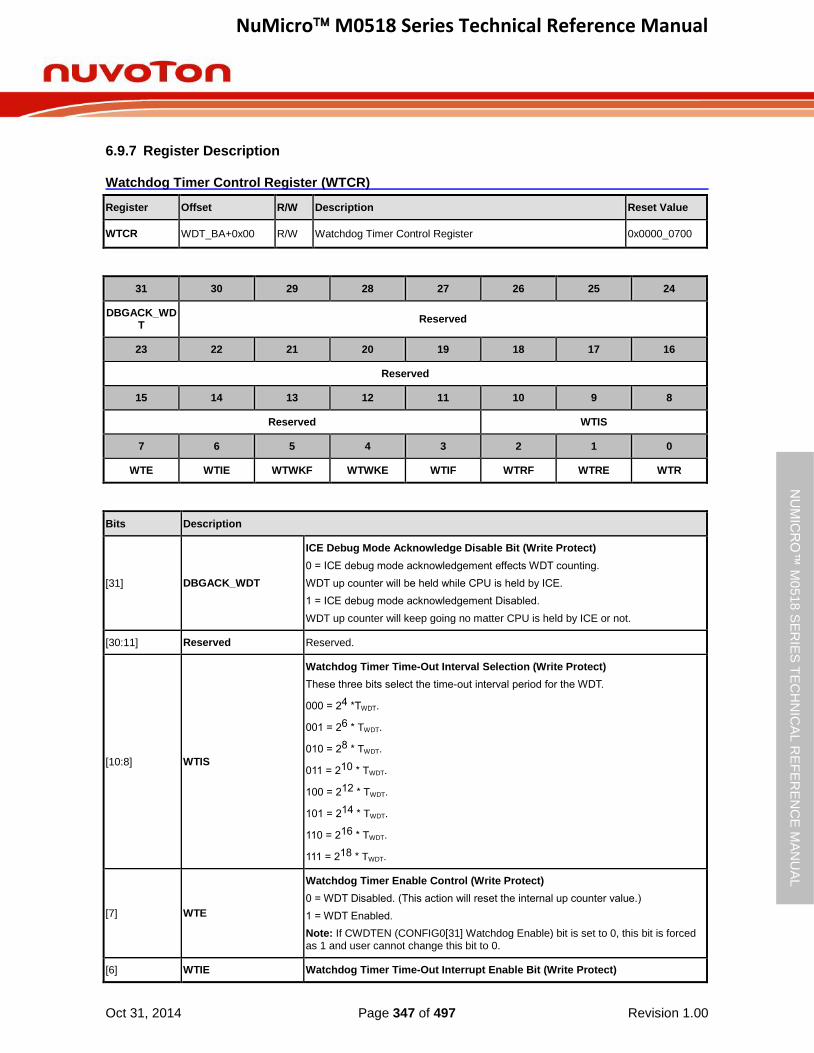
NuMicro M0518 Series Technical Reference Manual
Oct 31, 2014 Page 347 of 497 Revision 1.00
NU
MIC
RO
™ M
0518
SE
RIE
S T
EC
HN
ICA
L R
EF
ER
EN
CE
MA
NU
AL
6.9.7 Register Description
Watchdog Timer Control Register (WTCR)
Register Offset R/W Description Reset Value
WTCR WDT_BA+0x00 R/W Watchdog Timer Control Register 0x0000_0700
31 30 29 28 27 26 25 24
DBGACK_WDT
Reserved
23 22 21 20 19 18 17 16
Reserved
15 14 13 12 11 10 9 8
Reserved WTIS
7 6 5 4 3 2 1 0
WTE WTIE WTWKF WTWKE WTIF WTRF WTRE WTR
Bits Description
[31] DBGACK_WDT
ICE Debug Mode Acknowledge Disable Bit (Write Protect)
0 = ICE debug mode acknowledgement effects WDT counting.
WDT up counter will be held while CPU is held by ICE.
1 = ICE debug mode acknowledgement Disabled.
WDT up counter will keep going no matter CPU is held by ICE or not.
[30:11] Reserved Reserved.
[10:8] WTIS
Watchdog Timer Time-Out Interval Selection (Write Protect)
These three bits select the time-out interval period for the WDT.
000 = 24 *TWDT.
001 = 26 * TWDT.
010 = 28 * TWDT.
011 = 210 * TWDT.
100 = 212 * TWDT.
101 = 214 * TWDT.
110 = 216 * TWDT.
111 = 218 * TWDT.
[7] WTE
Watchdog Timer Enable Control (Write Protect)
0 = WDT Disabled. (This action will reset the internal up counter value.)
1 = WDT Enabled.
Note: If CWDTEN (CONFIG0[31] Watchdog Enable) bit is set to 0, this bit is forced as 1 and user cannot change this bit to 0.
[6] WTIE Watchdog Timer Time-Out Interrupt Enable Bit (Write Protect)

NuMicro M0518 Series Technical Reference Manual
Oct 31, 2014 Page 348 of 497 Revision 1.00
NU
MIC
RO
™ M
0518
SE
RIE
S T
EC
HN
ICA
L R
EF
ER
EN
CE
MA
NU
AL
If this bit is enabled, the WDT time-out interrupt signal is generated and inform to CPU.
0 = WDT time-out interrupt Disabled.
1 = WDT time-out interrupt Enabled.
[5] WTWKF
Watchdog Timer Time-Out Wake-Up Flag
This bit indicates the interrupt wake-up flag status of WDT.
0 = WDT does not cause chip wake-up.
1 = Chip wake-up from Idle or Power-down mode if WDT time-out interrupt signal generated.
Note: This bit is cleared by writing 1 to it.
[4] WTWKE
Watchdog Timer Time-Out Wake-Up Function Control (Write Protect)
If this bit is set to 1, while WTIF is generated to 1 and WTIE enabled, the WDT time-out interrupt signal will generate a wake-up trigger event to chip.
0 = Wake-up trigger event Disabled if WDT time-out interrupt signal generated.
1 = Wake-up trigger event Enabled if WDT time-out interrupt signal generated.
Note: Chip can be woken-up by WDT time-out interrupt signal generated only if WDT clock source is selected to 10 kHz oscillator.
[3] WTIF
Watchdog Timer Time-Out Interrupt Flag
This bit will set to 1 while WDT up counter value reaches the selected WDT time-out interval.
0 = WDT time-out interrupt did not occur.
1 = WDT time-out interrupt occurred.
Note: This bit is cleared by writing 1 to it.
[2] WTRF
Watchdog Timer Time-Out Reset Flag
This bit indicates the system has been reset by WDT time-out reset or not.
0 = WDT time-out reset did not occur.
1 = WDT time-out reset occurred.
Note: This bit is cleared by writing 1 to it.
[1] WTRE
Watchdog Timer Reset Enable Control (Write Protect)
Setting this bit will enable the WDT time-out reset function if the WDT up counter value has not been cleared after the specific WDT reset delay period expires.
0 = WDT time-out reset function Disabled.
1 = WDT time-out reset function Enabled.
[0] WTR
Reset Watchdog Timer Up Counter (Write Protect)
0 = No effect.
1 = Reset the internal 18-bit WDT up counter value.
Note: This bit will be automatically cleared by hardware.

NuMicro M0518 Series Technical Reference Manual
Oct 31, 2014 Page 349 of 497 Revision 1.00
NU
MIC
RO
™ M
0518
SE
RIE
S T
EC
HN
ICA
L R
EF
ER
EN
CE
MA
NU
AL
Watchdog Timer Alternative Control Register (WTCRALT)
Register Offset R/W Description Reset Value
WTCRALT WDT_BA+0x04 R/W Watchdog Timer Alternative Control Register 0x0000_0000
31 30 29 28 27 26 25 24
Reserved
23 22 21 20 19 18 17 16
Reserved
15 14 13 12 11 10 9 8
Reserved
7 6 5 4 3 2 1 0
Reserved WTRDSEL
Bits Description
[31:2] Reserved Reserved.
[1:0] WTRDSEL
Watchdog Timer Reset Delay Selection (Write Protect)
When WDT time-out happened, user has a time named WDT Reset Delay Period to clear WDT counter to prevent WDT time-out reset happened. User can select a suitable value of WDT Reset Delay Period for different WDT time-out period.
These bits are protected bit. It means programming this bit needs to write “59h”, “16h”, “88h” to address 0x5000_0100 to disable register protection. Reference the register REGWRPROT at address GCR_BA+0x100.
00 = Watchdog Timer Reset Delay Period is 1026 * WDT_CLK.
01 = Watchdog Timer Reset Delay Period is 130 * WDT_CLK.
10 = Watchdog Timer Reset Delay Period is 18 * WDT_CLK.
11 = Watchdog Timer Reset Delay Period is 3 * WDT_CLK.
Note: This register will be reset to 0 if WDT time-out reset happened.

NuMicro M0518 Series Technical Reference Manual
Oct 31, 2014 Page 350 of 497 Revision 1.00
NU
MIC
RO
™ M
0518
SE
RIE
S T
EC
HN
ICA
L R
EF
ER
EN
CE
MA
NU
AL
6.10 Window Watchdog Timer (WWDT)
6.10.1 Overview
The Window Watchdog Timer is used to perform a system reset within a specified window period to prevent software run to uncontrollable status by any unpredictable condition.
6.10.2 Features
6-bit down counter value (WWDTVAL[5:0]) and 6-bit compare window value (WWDTCR[21:16]) to make the WWDT time-out window period flexible
Supports 4-bit value to programmable maximum 11-bit prescale counter period of WWDT counter
6.10.3 Block Diagram
The Window Watchdog Timer clock control and block diagram are shown as follows.
10HCLK/2048
10 kHz LIRC
WWDT_S (CLKSEL2[17:16])
WDT_EN (APBCLK[0])
WWDT_CLK
11
Legend:
LIRC = Low-Speed Internal clock signal
00
01Reserved
Reserved
Figure 6-83 Window Watchdog Timer Clock Control
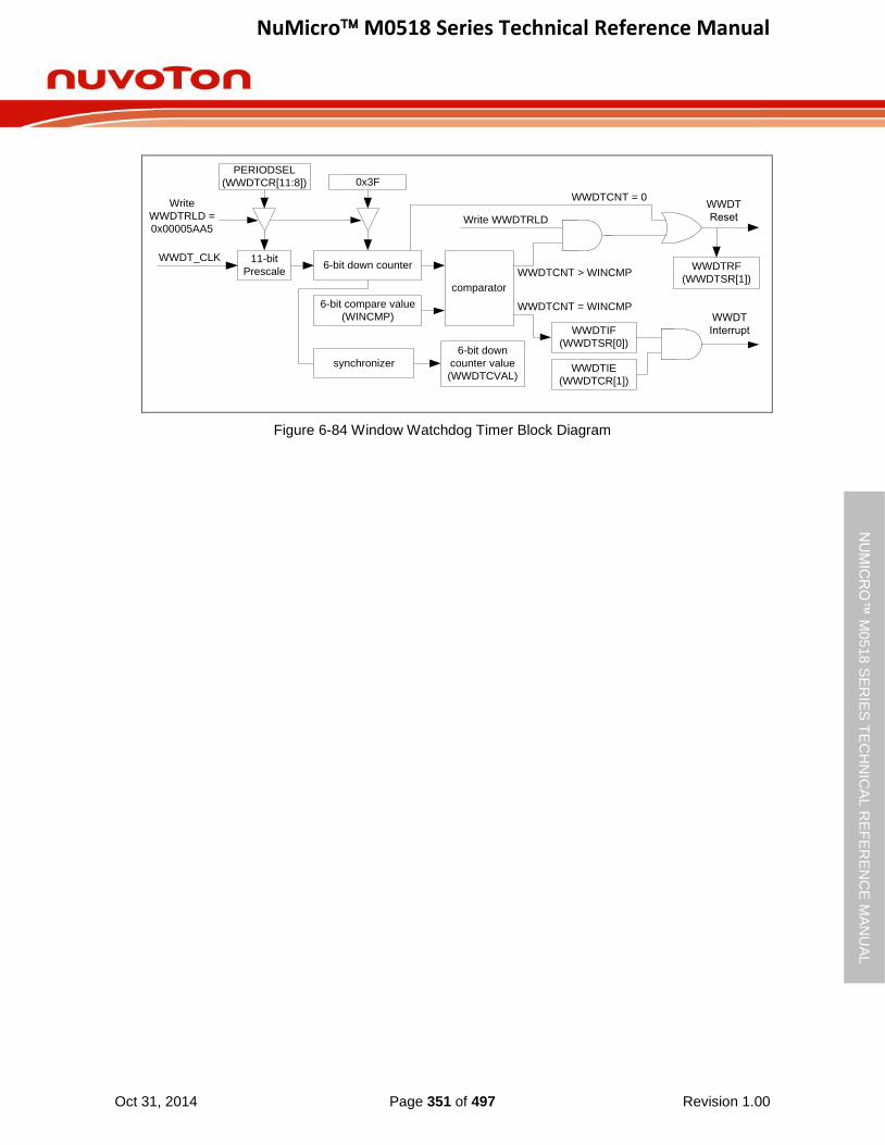
NuMicro M0518 Series Technical Reference Manual
Oct 31, 2014 Page 351 of 497 Revision 1.00
NU
MIC
RO
™ M
0518
SE
RIE
S T
EC
HN
ICA
L R
EF
ER
EN
CE
MA
NU
AL
6-bit down counter11-bit
Prescale
6-bit compare value
(WINCMP)
WWDT_CLK
0x3F
Write
WWDTRLD =
0x00005AA5
comparator
WWDTCNT = WINCMP
WWDTIF
(WWDTSR[0])
WWDTCNT > WINCMP
WWDTIE
(WWDTCR[1])
WWDT
Interrupt
WWDT
Reset
WWDTCNT = 0
Write WWDTRLD
WWDTRF
(WWDTSR[1])
PERIODSEL
(WWDTCR[11:8])
6-bit down
counter value
(WWDTCVAL)
synchronizer
Figure 6-84 Window Watchdog Timer Block Diagram
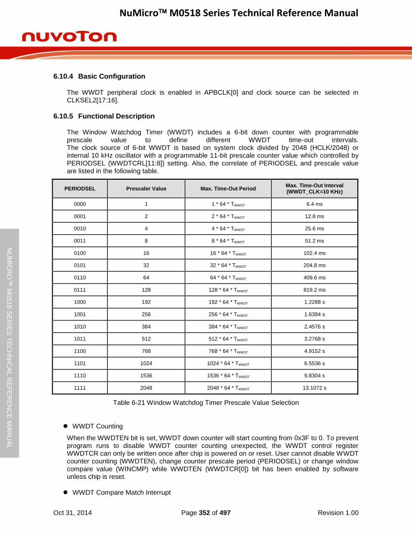
NuMicro M0518 Series Technical Reference Manual
Oct 31, 2014 Page 352 of 497 Revision 1.00
NU
MIC
RO
™ M
0518
SE
RIE
S T
EC
HN
ICA
L R
EF
ER
EN
CE
MA
NU
AL
6.10.4 Basic Configuration
The WWDT peripheral clock is enabled in APBCLK[0] and clock source can be selected in CLKSEL2[17:16].
6.10.5 Functional Description
The Window Watchdog Timer (WWDT) includes a 6-bit down counter with programmable prescale value to define different WWDT time-out intervals. The clock source of 6-bit WWDT is based on system clock divided by 2048 (HCLK/2048) or internal 10 kHz oscillator with a programmable 11-bit prescale counter value which controlled by PERIODSEL (WWDTCRL[11:8]) setting. Also, the correlate of PERIODSEL and prescale value are listed in the following table.
PERIODSEL Prescaler Value Max. Time-Out Period Max. Time-Out Interval (WWDT_CLK=10 KHz)
0000 1 1 * 64 * TWWDT 6.4 ms
0001 2 2 * 64 * TWWDT 12.8 ms
0010 4 4 * 64 * TWWDT 25.6 ms
0011 8 8 * 64 * TWWDT 51.2 ms
0100 16 16 * 64 * TWWDT 102.4 ms
0101 32 32 * 64 * TWWDT 204.8 ms
0110 64 64 * 64 * TWWDT 409.6 ms
0111 128 128 * 64 * TWWDT 819.2 ms
1000 192 192 * 64 * TWWDT 1.2288 s
1001 256 256 * 64 * TWWDT 1.6384 s
1010 384 384 * 64 * TWWDT 2.4576 s
1011 512 512 * 64 * TWWDT 3.2768 s
1100 768 768 * 64 * TWWDT 4.9152 s
1101 1024 1024 * 64 * TWWDT 6.5536 s
1110 1536 1536 * 64 * TWWDT 9.8304 s
1111 2048 2048 * 64 * TWWDT 13.1072 s
Table 6-21 Window Watchdog Timer Prescale Value Selection
WWDT Counting
When the WWDTEN bit is set, WWDT down counter will start counting from 0x3F to 0. To prevent program runs to disable WWDT counter counting unexpected, the WWDT control register WWDTCR can only be written once after chip is powered on or reset. User cannot disable WWDT counter counting (WWDTEN), change counter prescale period (PERIODSEL) or change window compare value (WINCMP) while WWDTEN (WWDTCR[0]) bit has been enabled by software unless chip is reset.
WWDT Compare Match Interrupt

NuMicro M0518 Series Technical Reference Manual
Oct 31, 2014 Page 353 of 497 Revision 1.00
NU
MIC
RO
™ M
0518
SE
RIE
S T
EC
HN
ICA
L R
EF
ER
EN
CE
MA
NU
AL
During down counting by the WWDT counter, the WWDTIF is set to 1 while the WWDT counter value (WWDTCVAL) is equal to WINCMP value and WWDTIF can be cleared by software; if WWDTIE is also set to 1 by software, the WWDT compare match interrupt signal is generated also while WWDTIF is set to 1 by hardware.
WWDT Reset System
When WWDTIF is generated, user must reload WWDT internal counter value to 0x3F by writing 0x00005AA5 to WWDTRLD. Otherwise, WWDT counter value will count down to 0 and generate WWDT reset system signal to info system reset.
If current WWDTCVAL value is larger than WINCMP value and user writes 0x00005AA5 to the WWDTRLD register, the WWDT reset system signal will be generated immediately to cause chip reset also.
0x3F
WWDTCVAL > WINCMPW
INC
MP
WWDTCVAL <= WINCMP 0x0
WWDTCVAL
Reset system when WWDTCVAL = 0
Write WWDTRLD 0x5AA5 here will reset system
Write WWDTRLD 0x5AA5 here will reload WWDTCVAL to 0x3F
Figure 6-85 Window Watchdog Timer Reset and Reload Behavior
WWDT Window Setting Limitation
When user writes 0x00005AA5 to WWDTRLD register to reload WWDT counter value to 0x3F, it needs 3 WWDT clocks to sync the reload command to actually perform reload action.
This means if user set PERIODSEL to 0000, the counter prescale value should be as 1, and the WINCMP value must be larger than 2; otherwise, writing WWDTRLD to reload WWDT counter value to 0x3F is unavailable while WWDTIF is generated and WWDT reset system event always happened.
PERIODSEL Prescale Value Valid WINCMP Value
0000 1 0x3 ~ 0x3F
0001 2 0x2 ~ 0x3F
Others Others 0x0 ~ 0x3F
Table 6-22 WINCMP Setting Limitation

NuMicro M0518 Series Technical Reference Manual
Oct 31, 2014 Page 354 of 497 Revision 1.00
NU
MIC
RO
™ M
0518
SE
RIE
S T
EC
HN
ICA
L R
EF
ER
EN
CE
MA
NU
AL
6.10.6 Register Map
R: read only, W: write only, R/W: both read and write
Register Offset R/W Description Reset Value
WWDT Base Address:
WWDT_BA = 0x4000_4100
WWDTRLD WWDT_BA+0x00 W Window Watchdog Timer Reload Counter Register 0x0000_0000
WWDTCR WWDT_BA+0x04 R/W Window Watchdog Timer Control Register 0x003F_0800
WWDTSR WWDT_BA+0x08 R/W Window Watchdog Timer Status Register 0x0000_0000
WWDTCVR WWDT_BA+0x0C R Window Watchdog Timer Counter Value Register 0x0000_003F

NuMicro M0518 Series Technical Reference Manual
Oct 31, 2014 Page 355 of 497 Revision 1.00
NU
MIC
RO
™ M
0518
SE
RIE
S T
EC
HN
ICA
L R
EF
ER
EN
CE
MA
NU
AL
6.10.7 Register Description
Window Watchdog Timer Reload Counter Register (WWDTRLD)
Register Offset R/W Description Reset Value
WWDTRLD WWDT_BA+0x00 W Window Watchdog Timer Reload Counter Register 0x0000_0000
31 30 29 28 27 26 25 24
WWDTRLD
23 22 21 20 19 18 17 16
WWDTRLD
15 14 13 12 11 10 9 8
WWDTRLD
7 6 5 4 3 2 1 0
WWDTRLD
Bits Description
[31:0] WWDTRLD
WWDT Reload Counter Register
Writing 0x00005AA5 to this register will reload the WWDT counter value to 0x3F.
Note: User can only write WWDTRLD to reload WWDT counter value when current WWDT counter value between 0 and WINCMP. If user writes WWDTRLD when current WWDT counter value is larger than WINCMP, WWDT reset signal will generate immediately.
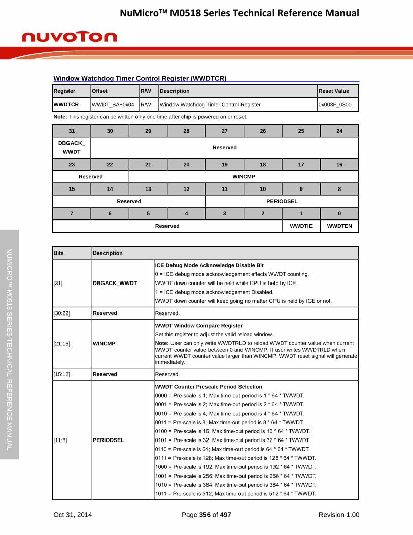
NuMicro M0518 Series Technical Reference Manual
Oct 31, 2014 Page 356 of 497 Revision 1.00
NU
MIC
RO
™ M
0518
SE
RIE
S T
EC
HN
ICA
L R
EF
ER
EN
CE
MA
NU
AL
Window Watchdog Timer Control Register (WWDTCR)
Register Offset R/W Description Reset Value
WWDTCR WWDT_BA+0x04 R/W Window Watchdog Timer Control Register 0x003F_0800
Note: This register can be written only one time after chip is powered on or reset.
31 30 29 28 27 26 25 24
DBGACK_
WWDT Reserved
23 22 21 20 19 18 17 16
Reserved WINCMP
15 14 13 12 11 10 9 8
Reserved PERIODSEL
7 6 5 4 3 2 1 0
Reserved WWDTIE WWDTEN
Bits Description
[31] DBGACK_WWDT
ICE Debug Mode Acknowledge Disable Bit
0 = ICE debug mode acknowledgement effects WWDT counting.
WWDT down counter will be held while CPU is held by ICE.
1 = ICE debug mode acknowledgement Disabled.
WWDT down counter will keep going no matter CPU is held by ICE or not.
[30:22] Reserved Reserved.
[21:16] WINCMP
WWDT Window Compare Register
Set this register to adjust the valid reload window.
Note: User can only write WWDTRLD to reload WWDT counter value when current WWDT counter value between 0 and WINCMP. If user writes WWDTRLD when current WWDT counter value larger than WINCMP, WWDT reset signal will generate immediately.
[15:12] Reserved Reserved.
[11:8] PERIODSEL
WWDT Counter Prescale Period Selection
0000 = Pre-scale is 1; Max time-out period is 1 * 64 * TWWDT.
0001 = Pre-scale is 2; Max time-out period is 2 * 64 * TWWDT.
0010 = Pre-scale is 4; Max time-out period is 4 * 64 * TWWDT.
0011 = Pre-scale is 8; Max time-out period is 8 * 64 * TWWDT.
0100 = Pre-scale is 16; Max time-out period is 16 * 64 * TWWDT.
0101 = Pre-scale is 32; Max time-out period is 32 * 64 * TWWDT.
0110 = Pre-scale is 64; Max time-out period is 64 * 64 * TWWDT.
0111 = Pre-scale is 128; Max time-out period is 128 * 64 * TWWDT.
1000 = Pre-scale is 192; Max time-out period is 192 * 64 * TWWDT.
1001 = Pre-scale is 256; Max time-out period is 256 * 64 * TWWDT.
1010 = Pre-scale is 384; Max time-out period is 384 * 64 * TWWDT.
1011 = Pre-scale is 512; Max time-out period is 512 * 64 * TWWDT.
NuMicro M0518 Series Technical Reference Manual
Oct 31, 2014 Page 357 of 497 Revision 1.00
NU
MIC
RO
™ M
0518
SE
RIE
S T
EC
HN
ICA
L R
EF
ER
EN
CE
MA
NU
AL
1100 = Pre-scale is 768; Max time-out period is 768 * 64 * TWWDT.
1101 = Pre-scale is 1024; Max time-out period is 1024 * 64 * TWWDT.
1110 = Pre-scale is 1536; Max time-out period is 1536 * 64 * TWWDT.
1111 = Pre-scale is 2048; Max time-out period is 2048 * 64 * TWWDT.
[7:2] Reserved Reserved.
[1] WWDTIE
WWDT Interrupt Enable Control
If this bit is enabled, the WWDT counter compare match interrupt signal is generated and inform to CPU.
0 = WWDT counter compare match interrupt Disabled.
1 = WWDT counter compare match interrupt Enabled.
[0] WWDTEN
WWDT Enable Control
Set this bit to enable WWDT counter counting.
0 = WWDT counter is stopped.
1 = WWDT counter is starting counting.
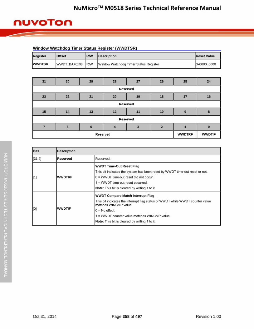
NuMicro M0518 Series Technical Reference Manual
Oct 31, 2014 Page 358 of 497 Revision 1.00
NU
MIC
RO
™ M
0518
SE
RIE
S T
EC
HN
ICA
L R
EF
ER
EN
CE
MA
NU
AL
Window Watchdog Timer Status Register (WWDTSR)
Register Offset R/W Description Reset Value
WWDTSR WWDT_BA+0x08 R/W Window Watchdog Timer Status Register 0x0000_0000
31 30 29 28 27 26 25 24
Reserved
23 22 21 20 19 18 17 16
Reserved
15 14 13 12 11 10 9 8
Reserved
7 6 5 4 3 2 1 0
Reserved WWDTRF WWDTIF
Bits Description
[31:2] Reserved Reserved.
[1] WWDTRF
WWDT Time-Out Reset Flag
This bit indicates the system has been reset by WWDT time-out reset or not.
0 = WWDT time-out reset did not occur.
1 = WWDT time-out reset occurred.
Note: This bit is cleared by writing 1 to it.
[0] WWDTIF
WWDT Compare Match Interrupt Flag
This bit indicates the interrupt flag status of WWDT while WWDT counter value matches WINCMP value.
0 = No effect.
1 = WWDT counter value matches WINCMP value.
Note: This bit is cleared by writing 1 to it.

NuMicro M0518 Series Technical Reference Manual
Oct 31, 2014 Page 359 of 497 Revision 1.00
NU
MIC
RO
™ M
0518
SE
RIE
S T
EC
HN
ICA
L R
EF
ER
EN
CE
MA
NU
AL
Window Watchdog Timer Counter Value Register (WWDTCVR)
Register Offset R/W Description Reset Value
WWDTCVR WWDT_BA+0x0C R Window Watchdog Timer Counter Value Register 0x0000_003F
31 30 29 28 27 26 25 24
Reserved
23 22 21 20 19 18 17 16
Reserved
15 14 13 12 11 10 9 8
Reserved
7 6 5 4 3 2 1 0
Reserved WWDTCVAL
Bits Description
[31:6] Reserved Reserved.
[5:0] WWDTCVAL WWDT Counter Value
WWDTCVAL will be updated continuously to monitor 6-bit down counter value.
NuMicro M0518 Series Technical Reference Manual
Oct 31, 2014 Page 360 of 497 Revision 1.00
NU
MIC
RO
™ M
0518
SE
RIE
S T
EC
HN
ICA
L R
EF
ER
EN
CE
MA
NU
AL
6.11 UART Interface Controller (UART)
6.11.1 Overview
The NuMicro M0518 series provides up to six channels of Universal Asynchronous Receiver/Transmitters (UART). UART0/UART1/UART2 supports 16 bytes entry FIFO and UART3/UART4/UART5 support 1 byte buffer for data payload. Besides, only UART0 and UART1 support the flow control function. The UART Controller performs a serial-to-parallel conversion on data received from the peripheral, and a parallel-to-serial conversion on data transmitted from the CPU. The UART controller also supports IrDA SIR Function. UART0/UART1 provides RS-485 function mode. UART0/UART1/UART2 provides LIN master/slave function.
6.11.2 Features
Full duplex, asynchronous communications
Separates receive / transmit 16/16 bytes (UART0/UART1/UART2 support) entry FIFO and 1/1 bytes buffer for data payloads (UART3/UART4/UART5 support)
Supports hardware auto-flow control function (CTS, RTS) and programmable RTS flow control trigger level (UART0/UART1 support).
Programmable receiver buffer trigger level
Supports programmable baud-rate generator for each channel individually
Supports CTS wake-up function (UART0/UART1 support)
Supports 7-bit receiver buffer time-out detection function
Programmable transmitting data delay time between the last stop and the next start bit by setting DLY (UA_TOR [15:8]) register
Supports break error, frame error, parity error and receive / transmit buffer overflow detect function
Fully programmable serial-interface characteristics
- Programmable data bit length, 5-, 6-, 7-, 8-bit character
- Programmable parity bit, even, odd, no parity or stick parity bit generation and detection
- Programmable stop bit length, 1, 1.5, or 2 stop bit generation
IrDA SIR function mode
- Supports 3/16-bit duration for normal mode
LIN function mode (UART0/UART1/UART2 support)
- Supports LIN master/slave mode
- Supports programmable break generation function for transmitter
- Supports break detect function for receiver
RS-485 function mode. (UART0/UART1 support)
- Supports RS-485 9-bit mode
- Supports hardware or software direct enable control provided by RTS pin.
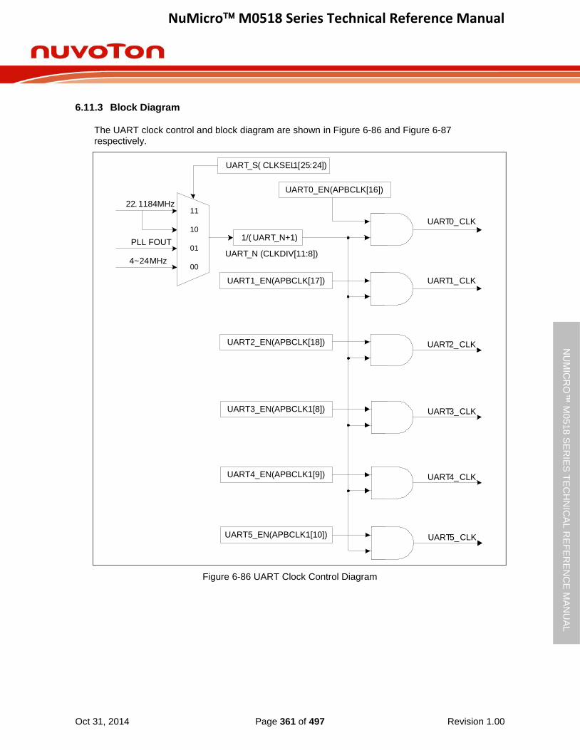
NuMicro M0518 Series Technical Reference Manual
Oct 31, 2014 Page 361 of 497 Revision 1.00
NU
MIC
RO
™ M
0518
SE
RIE
S T
EC
HN
ICA
L R
EF
ER
EN
CE
MA
NU
AL
6.11.3 Block Diagram
The UART clock control and block diagram are shown in Figure 6-86 and Figure 6-87 respectively.
11
10
01
00
PLL FOUT
4~24MHz
22. 1184MHz
UART0_CLK
UART1_EN(APBCLK[17]) UART1_CLK
UART2_CLK
1/( UART_N+1)
UART_N (CLKDIV[11:8])
UART_S( CLKSEL1[25:24])
UART3_CLK
UART4_CLK
UART5_CLK
UART2_EN(APBCLK[18])
UART0_EN(APBCLK[16])
UART3_EN(APBCLK1[8])
UART4_EN(APBCLK1[9])
UART5_EN(APBCLK1[10])
Figure 6-86 UART Clock Control Diagram
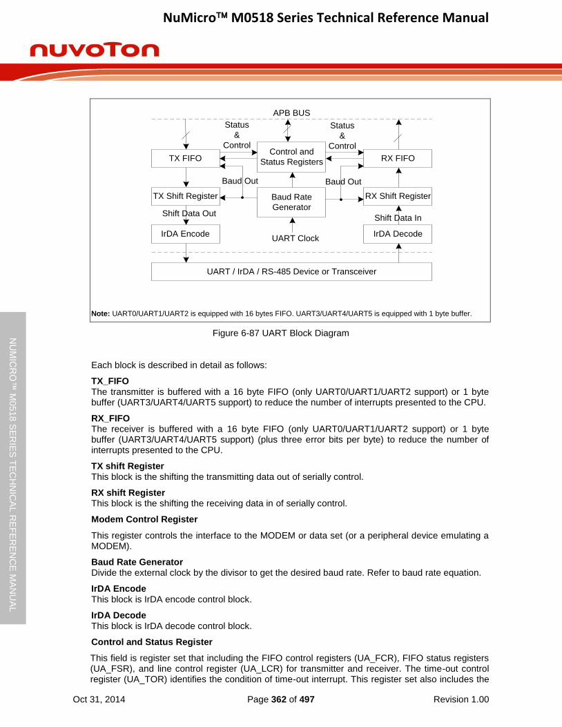
NuMicro M0518 Series Technical Reference Manual
Oct 31, 2014 Page 362 of 497 Revision 1.00
NU
MIC
RO
™ M
0518
SE
RIE
S T
EC
HN
ICA
L R
EF
ER
EN
CE
MA
NU
AL
APB BUS
TX FIFO
TX Shift Register
RX FIFO
RX Shift RegisterBaud Rate
Generator
Control and
Status Registers
IrDA DecodeIrDA Encode
UART / IrDA / RS-485 Device or Transceiver
UART Clock
Shift Data OutShift Data In
Baud Out Baud Out
Status
&
Control
Status
&
Control
Note: UART0/UART1/UART2 is equipped with 16 bytes FIFO. UART3/UART4/UART5 is equipped with 1 byte buffer.
Figure 6-87 UART Block Diagram
Each block is described in detail as follows:
TX_FIFO The transmitter is buffered with a 16 byte FIFO (only UART0/UART1/UART2 support) or 1 byte buffer (UART3/UART4/UART5 support) to reduce the number of interrupts presented to the CPU.
RX_FIFO The receiver is buffered with a 16 byte FIFO (only UART0/UART1/UART2 support) or 1 byte buffer (UART3/UART4/UART5 support) (plus three error bits per byte) to reduce the number of interrupts presented to the CPU.
TX shift Register This block is the shifting the transmitting data out of serially control.
RX shift Register This block is the shifting the receiving data in of serially control.
Modem Control Register
This register controls the interface to the MODEM or data set (or a peripheral device emulating a MODEM).
Baud Rate Generator Divide the external clock by the divisor to get the desired baud rate. Refer to baud rate equation.
IrDA Encode This block is IrDA encode control block.
IrDA Decode This block is IrDA decode control block.
Control and Status Register
This field is register set that including the FIFO control registers (UA_FCR), FIFO status registers (UA_FSR), and line control register (UA_LCR) for transmitter and receiver. The time-out control register (UA_TOR) identifies the condition of time-out interrupt. This register set also includes the
NuMicro M0518 Series Technical Reference Manual
Oct 31, 2014 Page 363 of 497 Revision 1.00
NU
MIC
RO
™ M
0518
SE
RIE
S T
EC
HN
ICA
L R
EF
ER
EN
CE
MA
NU
AL
interrupt enable register (UA_IER) and interrupt status register (UA_ISR) to enable or disable the responding interrupt and to identify the occurrence of the responding interrupt. There are ten types of interrupts, transmitter FIFO empty interrupt(THRE_INT), receiver threshold level reaching interrupt (RDA_INT), line status interrupt (parity error or framing error or break interrupt) (RLS_INT), time-out interrupt (TOUT_INT), MODEM status interrupt (MODEM_INT), Buffer error interrupt (BUF_ERR_INT), LIN receiver break field detected interrupt (LIN _INT), CTS Wake-up interrupt (CTSWKIF), Data Wake-up interrupt (DATAWKIF) and Auto-baud rate interrupt (ABRIF).
6.11.4 Basic Configuration
The UART Controller function pins are configured in GPB_MFP, GPD_MFP, ALT_MFP, ALT_MFP4 and ALT_MFP5 registers.
The UART Controller clock are enabled in UART0_EN (APBCLK[16]), UART1_EN (APBCLK[17]), UART2_EN (APBCLK[18]), UART3_EN (APBCLK1[8]), UART4_EN (APBCLK1[9]) and UART5_EN (APBCLK1[10]).
The UART Controller clock source is selected by UART_S (CLKSEL[25:24]).
The UART Controller clock prescaler is determined by UART_N (CLKDIV[11:8]).
UART Interface Controller Pin description is shown as following:
Pin Type Description
UART_TXD Output UART transmit
UART_RXD Input UART receive
UART_nCTS Input UART modem clear to send
UART_nRTS Output UART modem request to send
Table 6-23 UART Interface Controller Pin
6.11.5 Functional Description
The UART Controller supports four function modes including UART, IrDA, LIN and RS-485 mode. User can select a function by setting the UA_FUN_SEL register. The four function modes will be described in following section.
6.11.5.1 UART Controller Baud Rate Generator
The UART Controller includes a programmable baud rate generator capable of dividing clock input by divisors to produce the serial clock that transmitter and receiver need. The baud rate equation is Baud Rate = UART_CLK / (M * [BRD + 2]), where M and BRD are defined in Baud Rate Divider Register (UA_BAUD). The following tables list the UART baud rate equations in the various conditions and UART baud rate parameter settings. There is no error for the baud rate results calculated through the baud rate parameter and register setting below. In IrDA function mode, the baud rate generator must be set in Mode 0.
Mode DIV_X_EN DIV_X_ONE Divider X BRD Baud Rate Equation
0 0 0 Don’t care A UART_CLK / [16 * (A+2)].

NuMicro M0518 Series Technical Reference Manual
Oct 31, 2014 Page 364 of 497 Revision 1.00
NU
MIC
RO
™ M
0518
SE
RIE
S T
EC
HN
ICA
L R
EF
ER
EN
CE
MA
NU
AL
1 1 0 B A UART_CLK / [(B+1) * (A+2)], B must >= 8.
2 1 1 Don’t care A
UART_CLK / (BRD+2)
If UART_CLK <= 3*HCLK, A must >= 9.
If UART_CLK > 3*HCLK, A must >= 3*N – 1.
N is the smallest integer larger than or equal to the ratio of UART_CLK /HCLK.
For example,
if 3*HCLK < UART_CLK =< 4*HCLK, A must >=11.
if 4*HCLK < UART_CLK =< 5*HCLK, A must >=14.
Table 6-24 UART Baud Rate Equation
UART Peripheral Clock = 22.1184 MHz
Baud Rate Mode 0 Mode 1 Mode 2
921600 Not support A=0, B=11 A=22
460800 A=1 A=1, B=15 A=2, B=11
A=46
230400 A=4 A=4, B=15 A=6, B=11
A=94
115200 A=10 A=10, B=15 A=14, B=11
A=190
57600 A=22 A=22, B=15 A=30, B=11
A=382
38400 A=34 A=62, B=8
A=46, B=11 A=34, B=15
A=574
19200 A=70 A=126, B=8 A=94, B=11 A=70, B=15
A=1150
9600 A=142 A=254, B=8 A=190, B=11 A=142, B=15
A=2302
4800 A=286 A=510, B=8 A=382, B=11 A=286, B=15
A=4606
Table 6-25 UART Controller Baud Rate Parameter Setting Table
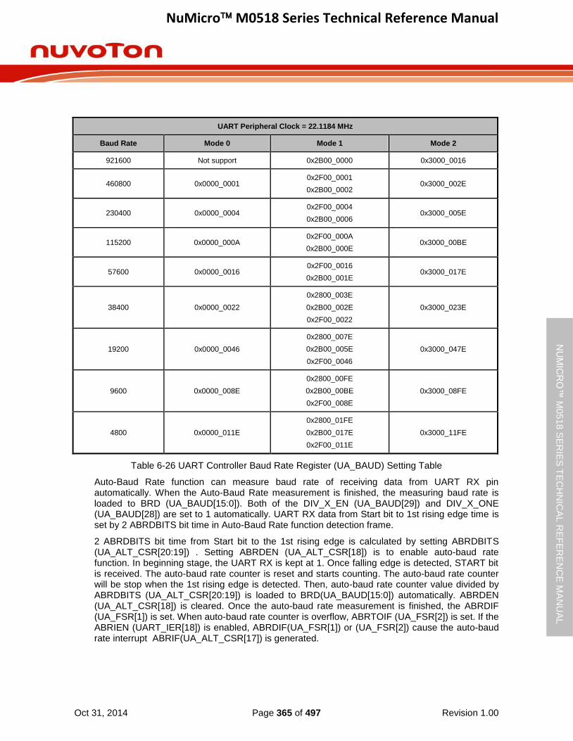
NuMicro M0518 Series Technical Reference Manual
Oct 31, 2014 Page 365 of 497 Revision 1.00
NU
MIC
RO
™ M
0518
SE
RIE
S T
EC
HN
ICA
L R
EF
ER
EN
CE
MA
NU
AL
UART Peripheral Clock = 22.1184 MHz
Baud Rate Mode 0 Mode 1 Mode 2
921600 Not support 0x2B00_0000 0x3000_0016
460800 0x0000_0001 0x2F00_0001
0x2B00_0002 0x3000_002E
230400 0x0000_0004 0x2F00_0004
0x2B00_0006 0x3000_005E
115200 0x0000_000A 0x2F00_000A
0x2B00_000E 0x3000_00BE
57600 0x0000_0016 0x2F00_0016
0x2B00_001E 0x3000_017E
38400 0x0000_0022
0x2800_003E
0x2B00_002E
0x2F00_0022
0x3000_023E
19200 0x0000_0046
0x2800_007E
0x2B00_005E
0x2F00_0046
0x3000_047E
9600 0x0000_008E
0x2800_00FE
0x2B00_00BE
0x2F00_008E
0x3000_08FE
4800 0x0000_011E
0x2800_01FE
0x2B00_017E
0x2F00_011E
0x3000_11FE
Table 6-26 UART Controller Baud Rate Register (UA_BAUD) Setting Table
Auto-Baud Rate function can measure baud rate of receiving data from UART RX pin automatically. When the Auto-Baud Rate measurement is finished, the measuring baud rate is loaded to BRD (UA_BAUD[15:0]). Both of the DIV_X_EN (UA_BAUD[29]) and DIV_X_ONE (UA_BAUD[28]) are set to 1 automatically. UART RX data from Start bit to 1st rising edge time is set by 2 ABRDBITS bit time in Auto-Baud Rate function detection frame.
2 ABRDBITS bit time from Start bit to the 1st rising edge is calculated by setting ABRDBITS (UA_ALT_CSR[20:19]) . Setting ABRDEN (UA_ALT_CSR[18]) is to enable auto-baud rate function. In beginning stage, the UART RX is kept at 1. Once falling edge is detected, START bit is received. The auto-baud rate counter is reset and starts counting. The auto-baud rate counter will be stop when the 1st rising edge is detected. Then, auto-baud rate counter value divided by ABRDBITS (UA_ALT_CSR[20:19]) is loaded to BRD(UA_BAUD[15:0]) automatically. ABRDEN (UA_ALT_CSR[18]) is cleared. Once the auto-baud rate measurement is finished, the ABRDIF (UA_FSR[1]) is set. When auto-baud rate counter is overflow, ABRTOIF (UA_FSR[2]) is set. If the ABRIEN (UART_IER[18]) is enabled, ABRDIF(UA_FSR[1]) or (UA_FSR[2]) cause the auto-baud rate interrupt ABRIF(UA_ALT_CSR[17]) is generated.
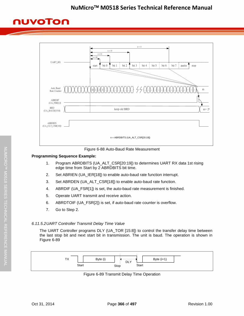
NuMicro M0518 Series Technical Reference Manual
Oct 31, 2014 Page 366 of 497 Revision 1.00
NU
MIC
RO
™ M
0518
SE
RIE
S T
EC
HN
ICA
L R
EF
ER
EN
CE
MA
NU
AL
BRD(UA_BAUD[15:0]
ABRDEN(UA_CLT_CSR[18])
start bit 1 bit 2bit 0 bit 3 bit 4 bit 5 bit 6UART_RX
0 1 2 3 ... ... ... ... ... ... ... ... ... ... ... ... ... ... ... ... ... ... ... ... ... ... ... ... ...
bit 7 parity stop
Auto Baud Rate Counter
ABRDIF(UA_FSR[1])
m
m÷ 2nkeep old BRD
n = ABRDBITS (UA_ALT_CSR[20:19])
n = 00
n = 01
n = 10
n = 11
Figure 6-88 Auto-Baud Rate Measurement
Programming Sequence Example:
1. Program ABRDBITS (UA_ALT_CSR[20:19]) to determines UART RX data 1st rising edge time from Start by 2 ABRDBITS bit time.
2. Set ABRIEN (UA_IER[18]) to enable auto-baud rate function interrupt.
3. Set ABRDEN (UA_ALT_CSR[18]) to enable auto-baud rate function.
4. ABRDIF (UA_FSR[1]) is set, the auto-baud rate measurement is finished.
5. Operate UART transmit and receive action.
6. ABRDTOIF (UA_FSR[2]) is set, if auto-baud rate counter is overflow.
7. Go to Step 2.
6.11.5.2 UART Controller Transmit Delay Time Value
The UART Controller programs DLY (UA_TOR [15:8]) to control the transfer delay time between the last stop bit and next start bit in transmission. The unit is baud. The operation is shown in Figure 6-89
Start
TX Byte (i) Byte (i+1)
Stop
DLYStart
Figure 6-89 Transmit Delay Time Operation

NuMicro M0518 Series Technical Reference Manual
Oct 31, 2014 Page 367 of 497 Revision 1.00
NU
MIC
RO
™ M
0518
SE
RIE
S T
EC
HN
ICA
L R
EF
ER
EN
CE
MA
NU
AL
6.11.5.3 UART Controller FIFO Control and Status
The UART0/UART1/UART2 are built-in with a 16-byte transmitter FIFO (TX_FIFO) and a 16-byte receiver FIFO (RX_FIFO) that reduces the number of interrupts presented to the CPU. The UART3/UART4/UART5 are equipped with 1-byte transmitter buffer and 1-byte receiver buffer.The CPU can read the status of the UART at any time during operation. The reported status information includes the type and condition of the transfer operations being performed by the UART, as well as 3 error conditions (parity error, framing error, break interrupt) probably occur while receiving data. This FIFO control and status also support all of UART, IrDA, LIN and RS-485 function mode.
6.11.5.4 UART Controller Wake-up Function
When the chip is in Power-down mode, an external CTS change will wake up chip from Power-down mode. This wake-up function is available in every function mode and it is supported for UART0 and UART1. User must enable the MODEN_INT interrupt to use the wake-up function.
6.11.5.5 UART Controller Interrupt and Status
UART Controller supports ten types of interrupts including:
Receiver threshold level reached interrupt (RDA_INT)
Transmitter FIFO empty interrupt (THRE_INT)
Line status interrupt (parity error, frame error or break interrupt) (RLS_INT)
MODEM status interrupt (MODEM_INT) (Only UART0/UART1 available)
Receiver buffer time-out interrupt (TOUT_INT)
Buffer error interrupt (BUF_ERR_INT)
LIN bus interrupt (LIN_ INT) (Only UART0/UART1/UART2 available)
CTS Wake-up interrupt (CTSWKIF) (Only UART0/UART1 available)
Data Wake-up interrupt (DATAWKIF)
Auto-baud rate interrupt (ABRIF)
The following tables describe the interrupt sources and flags. The interrupt is generated when the interrupt flag is generated and the interrupt enable bit is set. User must clear the interrupt flag after the interrupt is generated.
Interrupt Source Interrupt Indicator Interrupt Enable Bit
Interrupt Flag Flag Cleared By
Receive Data Available Interrupt
RDA_INT RDA_IEN RDA_IF Read UA_RBR
Transmit Holding Register Empty Interrupt
THRE_INT THRE_IEN THRE_IF Write UA_THR
Receive Line Status Interrupt
RLS_INT RLS_IEN
RLS_IF = BIF Writing “1” to BIF
RLS_IF = FEF Writing “1” to FEF
RLS_IF = PEF Writing “1” to PEF
RLS_IF = Writing ‘1’ to
NuMicro M0518 Series Technical Reference Manual
Oct 31, 2014 Page 368 of 497 Revision 1.00
NU
MIC
RO
™ M
0518
SE
RIE
S T
EC
HN
ICA
L R
EF
ER
EN
CE
MA
NU
AL
RS485_ADD_DETF RS485_ADD_DETF
Modem Status Interrupt
MODEM_INT MODEM_IEN MODEM_IF = DCTSF Write “1” to DCTSF
RX Time-out Interrupt TOUT_INT TOUT_IEN TOUT_IF Read UA_RBR
Buffer Error Interrupt BUF_ERR_INT BUF_ERR_IEN
BUF_ERR_IF =TX_OVER_IF
Write “1” to TX_OVER_IF
BUF_ERR_IF = RX_OVER_IF
Write “1” to RX_OVER_IF
LIN Bus Interrupt LIN_ _INT LIN _IEN
LIN_IF = LIN_BKDET_F Write “1” to LIN_IF and
Write “1” to LIN_BKDET_F
LIN_IF = BIT_ERR_F Write “1” to BIT_ERR_F
LIN_IF = LIN_IDPERR_F Write “1” to o LIN_IDPERR_F
LIN_IF = LINS_HERR_F Write “1” to LINS_HERR_F
LIN_IF = LINS_HDET_F Write “1” to LINS_HDET_F
nCTS wakeup interrupt
N/A WKCTSIEN CTSWKIF Write ‘1’ to CTSWKIF
Data wakeup interrupt N/A WKDATIEN DATWKIF Write ‘1’ to DATWKIF
Auto-baud rate interrupt
N/A ABRIEN ABRIF = ABRDIF Write ‘1’ to ABRDIF
ABRIF = ABRDTOIF Write ‘1’ to ABRDTOIF.
Table 6-27 UART Controller Interrupt Source and Flag List
6.11.5.6 UART Function Mode
The UART Controller provides UART function (user must set UA_FUN_SEL [1:0] to “00” to enable UART function mode). The UART baud rate is up to 1 Mbps.
The UART provides full-duplex and asynchronous communications. The transmitter and receiver contain 16 bytes FIFO for payloads. User can program receiver buffer trigger level and receiver buffer time-out detection for receiver. The transmitting data delay time between the last stop and the next start bit can be programed by setting DLY (UA_TOR [15:8]) register. The UART supports hardware auto-flow control and flow control function (CTS, RTS), programmable RTS flow control trigger level and fully programmable serial-interface characteristics.
UART Line Control Function
The UART Controller supports fully programmable serial-interface characteristics by setting the UA_LCR register. Software can use the UA_LCR register to program the word length, stop bit and parity bit. The following tables list the UART word and stop bit length settings and the UART parity bit settings.
NSB (UA_LCR[2])
WLS (UA_LCR[1:0])
Word Length (Bit) Stop Length (Bit)
0 00 5 1
0 01 6 1

NuMicro M0518 Series Technical Reference Manual
Oct 31, 2014 Page 369 of 497 Revision 1.00
NU
MIC
RO
™ M
0518
SE
RIE
S T
EC
HN
ICA
L R
EF
ER
EN
CE
MA
NU
AL
0 10 7 1
0 11 8 1
1 00 5 1.5
1 01 6 2
1 10 7 2
1 11 8 2
Table 6-28 UART Line Control of Word and Stop Length Setting
Parity Type SPE
(UA_LCR[5]) EPE
(UA_LCR[4]) PBE
(UA_LCR[3]) Description
No Parity x x 0 No parity bit output.
Odd Parity 0 0 1 Odd Parity is calculated by adding all the “1’s” in a data stream and adding a parity bit to the total bits, to make the total count an odd number.
Even Parity 0 1 1 Even Parity is calculated by adding all the “1’s” in a data stream and adding a parity bit to the total bits, to make the count an even number.
Forced Mask Parity
1 0 1
Parity bit always logic 1.
Parity bit on the serial byte is set to “1” regardless of total number of “1’s” (even or odd counts).
Forced Space Parity
1 1 1
Parity bit always logic 0.
Parity bit on the serial byte is set to “0” regardless of total number of “1’s” (even or odd counts).
Table 6-29 UART Line Control of Parity Bit Setting
UART Auto-Flow Control Function
The UART supports auto-flow control function that uses two signals, CTS (clear-to-send) and RTS (request-to-send), to control the flow of data transfer between the UART and external devices (e.g. Modem). When auto flow is enabled, the UART is not allowed to receive data until the UART asserts RTS to external device. When the number of bytes in the RX FIFO equals the value of RTS_TRI_LEV (UA_FCR [19:16]), the RTS is de-asserted. The UART sends data out when UART detects CTS is asserted from external device. If the valid asserted CTS is not detected, the UART will not send data out.
The following diagram demonstrates the auto-flow control block.
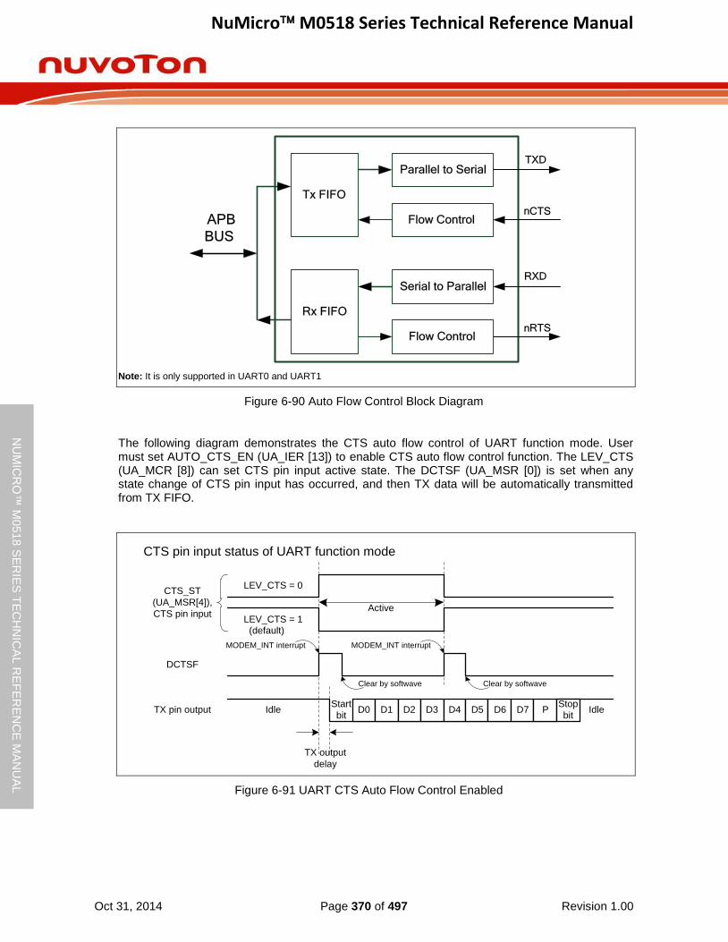
NuMicro M0518 Series Technical Reference Manual
Oct 31, 2014 Page 370 of 497 Revision 1.00
NU
MIC
RO
™ M
0518
SE
RIE
S T
EC
HN
ICA
L R
EF
ER
EN
CE
MA
NU
AL
Tx FIFO
Parallel to Serial
CTSFlow Control
Rx FIFO
Serial to Parallel
RTSFlow Control
APB
BUS
n
n
TXD
RXD
Note: It is only supported in UART0 and UART1
Figure 6-90 Auto Flow Control Block Diagram
The following diagram demonstrates the CTS auto flow control of UART function mode. User must set AUTO_CTS_EN (UA_IER [13]) to enable CTS auto flow control function. The LEV_CTS (UA_MCR [8]) can set CTS pin input active state. The DCTSF (UA_MSR [0]) is set when any state change of CTS pin input has occurred, and then TX data will be automatically transmitted from TX FIFO.
LEV_CTS = 0
LEV_CTS = 1
CTS_ST
(UA_MSR[4]),
CTS pin inputActive
CTS pin input status of UART function mode
D0 D1 D2 D3 D4 D5 D6 D7 PStart
bit
Stop
bitTX pin output
DCTSF
MODEM_INT interrupt
Clear by softwave
MODEM_INT interrupt
Clear by softwave
Idle Idle
TX output
delay
(default)
Figure 6-91 UART CTS Auto Flow Control Enabled
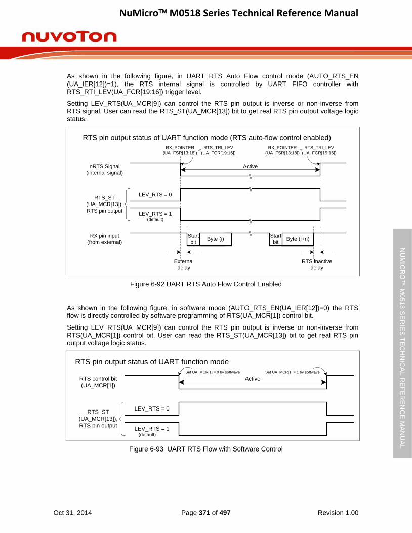
NuMicro M0518 Series Technical Reference Manual
Oct 31, 2014 Page 371 of 497 Revision 1.00
NU
MIC
RO
™ M
0518
SE
RIE
S T
EC
HN
ICA
L R
EF
ER
EN
CE
MA
NU
AL
As shown in the following figure, in UART RTS Auto Flow control mode (AUTO_RTS_EN (UA_IER[12])=1), the RTS internal signal is controlled by UART FIFO controller with RTS_RTI_LEV(UA_FCR[19:16]) trigger level.
Setting LEV_RTS(UA_MCR[9]) can control the RTS pin output is inverse or non-inverse from RTS signal. User can read the RTS_ST(UA_MCR[13]) bit to get real RTS pin output voltage logic status.
LEV_RTS = 1
LEV_RTS = 0
nRTS Signal
(internal signal)
Active
RTS pin output status of UART function mode (RTS auto-flow control enabled)
Byte (i) Byte (i+n)Start
bit
RX pin input
(from external)
RTS inactive
delay
External
delay
Start
bit
RX_POINTER
(UA_FSR[13:18])
RTS_TRI_LEV
(UA_FCR[19:16])<
RX_POINTER
(UA_FSR[13:18])
RTS_TRI_LEV
(UA_FCR[19:16])=
RTS_ST
(UA_MCR[13]),
RTS pin output
(default)
Figure 6-92 UART RTS Auto Flow Control Enabled
As shown in the following figure, in software mode (AUTO_RTS_EN(UA_IER[12])=0) the RTS flow is directly controlled by software programming of RTS(UA_MCR[1]) control bit.
Setting LEV_RTS(UA_MCR[9]) can control the RTS pin output is inverse or non-inverse from RTS(UA_MCR[1]) control bit. User can read the RTS_ST(UA_MCR[13]) bit to get real RTS pin output voltage logic status.
LEV_RTS = 1
LEV_RTS = 0
RTS control bit
(UA_MCR[1])
RTS_ST
(UA_MCR[13]),
RTS pin output
Active
RTS pin output status of UART function mode
Set UA_MCR[1] = 0 by softwave Set UA_MCR[1] = 1 by softwave
(default)
Figure 6-93 UART RTS Flow with Software Control
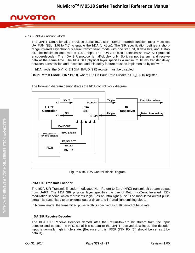
NuMicro M0518 Series Technical Reference Manual
Oct 31, 2014 Page 372 of 497 Revision 1.00
NU
MIC
RO
™ M
0518
SE
RIE
S T
EC
HN
ICA
L R
EF
ER
EN
CE
MA
NU
AL
6.11.5.7 IrDA Function Mode
The UART Controller also provides Serial IrDA (SIR, Serial Infrared) function (user must set UA_FUN_SEL [1:0] to ’10’ to enable the IrDA function). The SIR specification defines a short-range infrared asynchronous serial transmission mode with one start bit, 8 data bits, and 1 stop bit. The maximum data rate is 115.2 kbps. The IrDA SIR block contains an IrDA SIR protocol encoder/decoder. The IrDA SIR protocol is half-duplex only. So it cannot transmit and receive data at the same time. The IrDA SIR physical layer specifies a minimum 10 ms transfer delay between transmission and reception, and this delay feature must be implemented by software.
In IrDA mode, the DIV_X_EN (UA_BAUD [29]) register must be disabled.
Baud Rate = Clock / (16 * BRD), where BRD is Baud Rate Divider in UA_BAUD register.
The following diagram demonstrates the IrDA control block diagram.
UART
Controller
TX
RX
IrDA
SIR
IR_SOUT
IR_SIN
SOUT
SIN
IR
Transceiver
Emit Infra red ray
Detect Infra red ray
IRCR
BAUDOUT
IrDA_Enable
TX_SELECT
INV_TX
INV_RX
TX pin
RX pin
FUN_SEL=10b
(UA_FUN_SEL[1:0])
Figure 6-94 IrDA Control Block Diagram
IrDA SIR Transmit Encoder
The IrDA SIR Transmit Encoder modulates Non-Return-to Zero (NRZ) transmit bit stream output from UART. The IrDA SIR physical layer specifies the use of Return-to-Zero, Inverted (RZI) modulation scheme which represents logic 0 as an infra light pulse. The modulated output pulse stream is transmitted to an external output driver and infrared light emitting diode.
In Normal mode, the transmitted pulse width is specified as 3/16 period of baud rate.
IrDA SIR Receive Decoder
The IrDA SIR Receive Decoder demodulates the Return-to-Zero bit stream from the input detector and outputs the NRZ serial bits stream to the UART received data input. The decoder input is normally high in idle state. (Because of this, IRCR (INV_RX [6]) should be set as 1 by default).

NuMicro M0518 Series Technical Reference Manual
Oct 31, 2014 Page 373 of 497 Revision 1.00
NU
MIC
RO
™ M
0518
SE
RIE
S T
EC
HN
ICA
L R
EF
ER
EN
CE
MA
NU
AL
A start bit is detected when the decoder input is LOW.
IrDA SIR Operation
The IrDA SIR encoder/decoder provides functionality which converts between UART data stream and half-duplex serial SIR interface. The following diagram is IrDA encoder/decoder waveform.
SOUT
(from UART TX)
IR_SOUT
(encoder output)
IR_SIN
(decorder input)
SIN
(to UART RX)
0 0 1 0 1 1 1 0 0 11
1
Bit cycle width
3/16 bit width
STOP BITSTART BIT
IrDA
TX Timing
IrDA
RX Timing
0 1 0 0 1 0 1 0 0
START BIT STOP BIT
3/16 bit width
1
Figure 6-95 IrDA TX/RX Timing Diagram
6.11.5.8 LIN (Local Interconnection Network) Mode
The UART0/UART1/UART2 supports LIN function. Setting FUN_SEL (UA_FUN_SEL[1:0]) to ’01’ to select LIN mode operation. The UART0/UART1/UART2 supports LIN break/delimiter generation and break/delimiter detection in LIN master mode, and supports header detection and automatic resynchronization in LIN Slave mode.
6.11.5.8.1 Structure of LIN Frame
According to the LIN protocol, all information transmitted is packed as frames; a frame consists of a header (provided by the master task) and a response (provided by a slave task), followed by a response (provided by a slave task). The header (provided by the master task) consists of a break field and a sync field followed by a frame identifier (frame ID). The frame identifier uniquely defines the purpose of the frame. The slave task is appointed for providing the response associated with the frame ID. The response consists of a data field and a checksum field. The following diagram is the structure of LIN Frame.

NuMicro M0518 Series Technical Reference Manual
Oct 31, 2014 Page 374 of 497 Revision 1.00
NU
MIC
RO
™ M
0518
SE
RIE
S T
EC
HN
ICA
L R
EF
ER
EN
CE
MA
NU
AL
Data 1 Data 2 Data N Check
Sum
Protected
Identifier
field
Header
Response
spaceResponse
Inter-
frame
space
Frame
Frame slot
Synch
field
Break
Field
Figure 6-96 Structure of LIN Frame
6.11.5.8.2 Structure of LIN Byte
In LIN mode, each byte field is initiated by a START bit with value 0 (dominant), followed by 8 data bits and no parity bit, LSB is first and ended by 1 stop bit with value 1 (recessive) in accordance with the LIN standard. The structure of Byte is shown as follows.
Start
bit
LSB
(bit 0) (bit 1) (bit 2) (bit 3) (bit 4) (bit 5)
MSB
(bit 7)(bit 6)
Stop
bit
Byte field
LIN Bus
Figure 6-97 Structure of LIN Byte
6.11.5.8.3 LIN Master Mode
The UART0/UART1/UART2 controllers support LIN Master mode. To enable and initialize the LIN Master mode, the following steps are necessary:
1. Setting the UA_BAUD register to select the desired baud rate.
2. Setting WLS (UA_LCR[1:0]) to “11” to configure the data length with 8 bits, clearing PBE (UA_LCR[3]) bit to disable parity check and clearing NSB (UA_LCR[2]) bit to configure with one stop bit.
3. Setting FUN_SEL (UA_FUN_SEL[1:0]) to “01” to select LIN function mode operation.
A complete header consists of a break field and sync field followed by a frame identifier (frame ID). The UART0/UART1/UART2 controller can be selected header sending by three header selected modes. The header selected mode can be “break field” or “break field and sync field” or “break field, sync field and frame ID field” by setting LIN_HEAD_SEL (UA_LIN_CTL[23:22]). If the selected header is “break field”, software must handle the following sequence to send a complete header to bus by filling sync data (0x55) and frame ID data to the UA_THR register. If the selected header is “break field and sync field”, software must handle the sequence to send a complete header to bus by filling the frame ID data to UA_THR register, and if the selected header is “break field, sync field and frame ID field”, hardware will control the header sending sequence automatically but software must filled frame ID data to LIN_PID (UA_LIN_CTL [31:24]). When operating in header selected mode in which the selected header is “break field, sync field and frame ID field”, the frame ID parity bit can be calculated by software or hardware depending whether the LIN_IDPEN (UA_LIN_CTL[9]) bit is set or not.
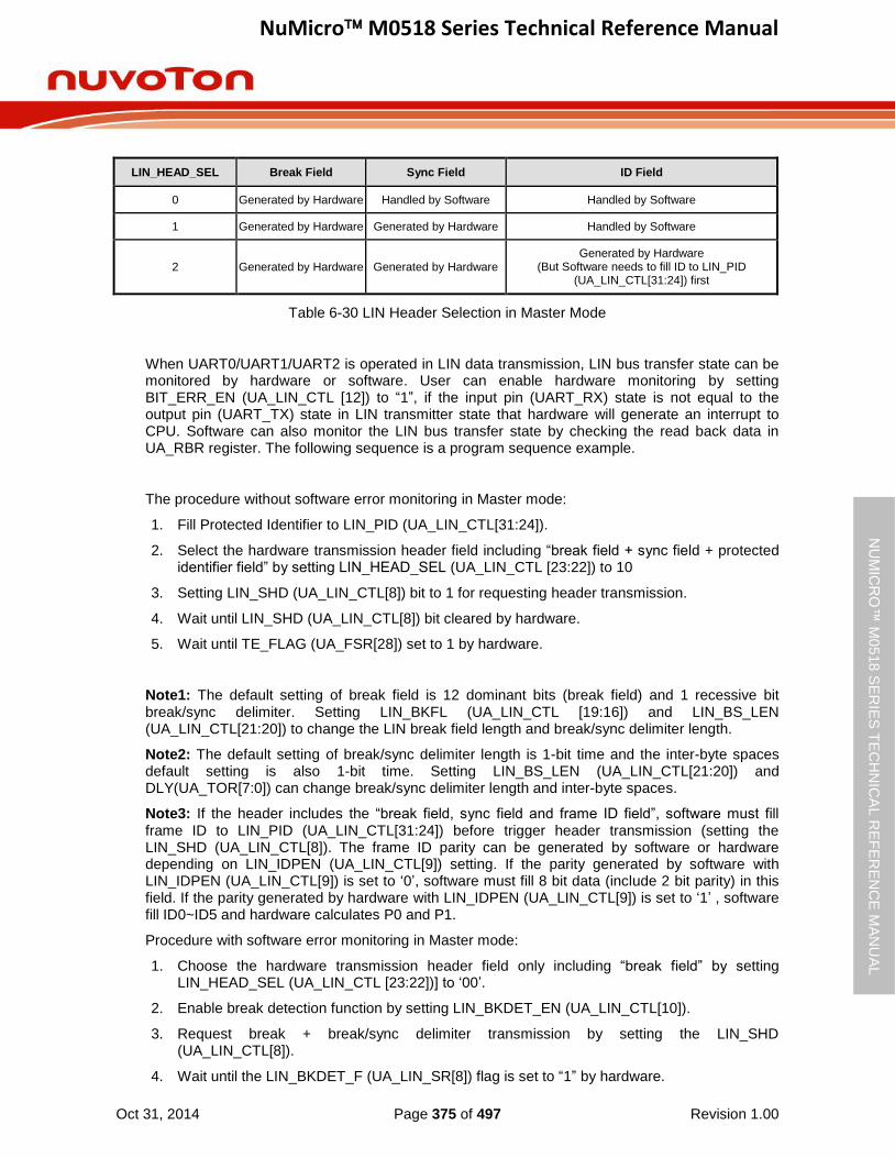
NuMicro M0518 Series Technical Reference Manual
Oct 31, 2014 Page 375 of 497 Revision 1.00
NU
MIC
RO
™ M
0518
SE
RIE
S T
EC
HN
ICA
L R
EF
ER
EN
CE
MA
NU
AL
LIN_HEAD_SEL Break Field Sync Field ID Field
0 Generated by Hardware Handled by Software Handled by Software
1 Generated by Hardware Generated by Hardware Handled by Software
2 Generated by Hardware Generated by Hardware Generated by Hardware
(But Software needs to fill ID to LIN_PID (UA_LIN_CTL[31:24]) first
Table 6-30 LIN Header Selection in Master Mode
When UART0/UART1/UART2 is operated in LIN data transmission, LIN bus transfer state can be monitored by hardware or software. User can enable hardware monitoring by setting BIT_ERR_EN (UA_LIN_CTL [12]) to “1”, if the input pin (UART_RX) state is not equal to the output pin (UART_TX) state in LIN transmitter state that hardware will generate an interrupt to CPU. Software can also monitor the LIN bus transfer state by checking the read back data in UA_RBR register. The following sequence is a program sequence example.
The procedure without software error monitoring in Master mode:
1. Fill Protected Identifier to LIN_PID (UA_LIN_CTL[31:24]).
2. Select the hardware transmission header field including “break field + sync field + protected identifier field” by setting LIN_HEAD_SEL (UA_LIN_CTL [23:22]) to 10
3. Setting LIN_SHD (UA_LIN_CTL[8]) bit to 1 for requesting header transmission.
4. Wait until LIN_SHD (UA_LIN_CTL[8]) bit cleared by hardware.
5. Wait until TE_FLAG (UA_FSR[28]) set to 1 by hardware.
Note1: The default setting of break field is 12 dominant bits (break field) and 1 recessive bit break/sync delimiter. Setting LIN_BKFL (UA_LIN_CTL [19:16]) and LIN_BS_LEN (UA_LIN_CTL[21:20]) to change the LIN break field length and break/sync delimiter length.
Note2: The default setting of break/sync delimiter length is 1-bit time and the inter-byte spaces default setting is also 1-bit time. Setting LIN_BS_LEN (UA_LIN_CTL[21:20]) and DLY(UA_TOR[7:0]) can change break/sync delimiter length and inter-byte spaces.
Note3: If the header includes the “break field, sync field and frame ID field”, software must fill frame ID to LIN_PID (UA_LIN_CTL[31:24]) before trigger header transmission (setting the LIN_SHD (UA_LIN_CTL[8]). The frame ID parity can be generated by software or hardware depending on LIN_IDPEN (UA_LIN_CTL[9]) setting. If the parity generated by software with LIN_IDPEN (UA_LIN_CTL[9]) is set to ‘0’, software must fill 8 bit data (include 2 bit parity) in this field. If the parity generated by hardware with LIN_IDPEN (UA_LIN_CTL[9]) is set to ‘1’ , software fill ID0~ID5 and hardware calculates P0 and P1.
Procedure with software error monitoring in Master mode:
1. Choose the hardware transmission header field only including “break field” by setting LIN_HEAD_SEL (UA_LIN_CTL [23:22])] to ‘00’.
2. Enable break detection function by setting LIN_BKDET_EN (UA_LIN_CTL[10]).
3. Request break + break/sync delimiter transmission by setting the LIN_SHD (UA_LIN_CTL[8]).
4. Wait until the LIN_BKDET_F (UA_LIN_SR[8]) flag is set to “1” by hardware.
NuMicro M0518 Series Technical Reference Manual
Oct 31, 2014 Page 376 of 497 Revision 1.00
NU
MIC
RO
™ M
0518
SE
RIE
S T
EC
HN
ICA
L R
EF
ER
EN
CE
MA
NU
AL
5. Request sync field transmission by writing 0x55 into UA_THR register.
6. Wait until the RDA_IF (UA_ISR[0]) is set to “1” by hardware and then read back the UA_RBR register.
7. Request header frame ID transmission by writing the protected identifier value to UA_THR register.
8. Wait until the RDA_IF (UA_ISR[0]) is set to “1” by hardware and then read back the UA_RBR register.
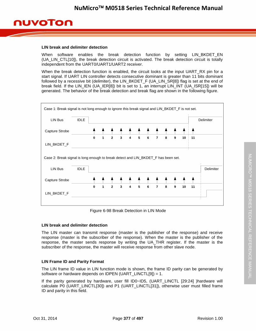
NuMicro M0518 Series Technical Reference Manual
Oct 31, 2014 Page 377 of 497 Revision 1.00
NU
MIC
RO
™ M
0518
SE
RIE
S T
EC
HN
ICA
L R
EF
ER
EN
CE
MA
NU
AL
LIN break and delimiter detection
When software enables the break detection function by setting LIN_BKDET_EN (UA_LIN_CTL[10]), the break detection circuit is activated. The break detection circuit is totally independent from the UART0/UART1/UART2 receiver.
When the break detection function is enabled, the circuit looks at the input UART_RX pin for a start signal. If UART LIN controller detects consecutive dominant is greater than 11 bits dominant followed by a recessive bit (delimiter), the LIN_BKDET_F (UA_LIN_SR[8]) flag is set at the end of break field. If the LIN_IEN (UA_IER[8]) bit is set to 1, an interrupt LIN_INT (UA_ISR[15]) will be generated. The behavior of the break detection and break flag are shown in the following figure.
LIN Bus IDLE
Capture Strobe
0
Delimiter
LIN_BKDET_F
1 2 3 4 5 6 7 8 9 10 11
Case 2: Break signal is long enough to break detect and LIN_BKDET_F has been set.
LIN Bus IDLE
Capture Strobe
0
Delimiter
LIN_BKDET_F
1 2 3 4 5 6 7 8 9 10 11
Case 1: Break signal is not long enough to ignore this break signal and LIN_BKDET_F is not set.
Figure 6-98 Break Detection in LIN Mode
LIN break and delimiter detection
The LIN master can transmit response (master is the publisher of the response) and receive response (master is the subscriber of the response). When the master is the publisher of the response, the master sends response by writing the UA_THR register. If the master is the subscriber of the response, the master will receive response from other slave node.
LIN Frame ID and Parity Format
The LIN frame ID value in LIN function mode is shown, the frame ID parity can be generated by software or hardware depends on IDPEN (UART_LINCTL[9]) = 1.
If the parity generated by hardware, user fill ID0~ID5, (UART_LINCTL [29:24] )hardware will calculate P0 (UART_LINCTL[30]) and P1 (UART_LINCTL[31]), otherwise user must filled frame ID and parity in this field.
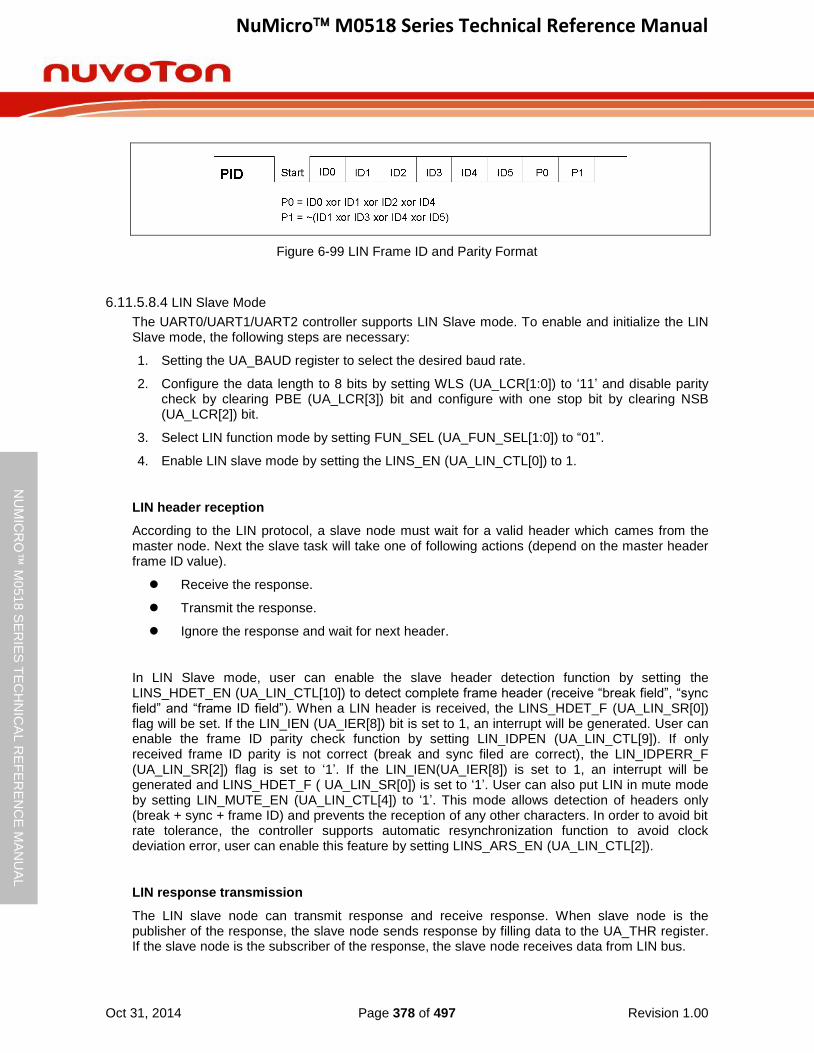
NuMicro M0518 Series Technical Reference Manual
Oct 31, 2014 Page 378 of 497 Revision 1.00
NU
MIC
RO
™ M
0518
SE
RIE
S T
EC
HN
ICA
L R
EF
ER
EN
CE
MA
NU
AL
Figure 6-99 LIN Frame ID and Parity Format
6.11.5.8.4 LIN Slave Mode
The UART0/UART1/UART2 controller supports LIN Slave mode. To enable and initialize the LIN Slave mode, the following steps are necessary:
1. Setting the UA_BAUD register to select the desired baud rate.
2. Configure the data length to 8 bits by setting WLS (UA_LCR[1:0]) to ‘11’ and disable parity check by clearing PBE (UA_LCR[3]) bit and configure with one stop bit by clearing NSB (UA_LCR[2]) bit.
3. Select LIN function mode by setting FUN_SEL (UA_FUN_SEL[1:0]) to “01”.
4. Enable LIN slave mode by setting the LINS_EN (UA_LIN_CTL[0]) to 1.
LIN header reception
According to the LIN protocol, a slave node must wait for a valid header which cames from the master node. Next the slave task will take one of following actions (depend on the master header frame ID value).
Receive the response.
Transmit the response.
Ignore the response and wait for next header.
In LIN Slave mode, user can enable the slave header detection function by setting the LINS_HDET_EN (UA_LIN_CTL[10]) to detect complete frame header (receive “break field”, “sync field” and “frame ID field”). When a LIN header is received, the LINS_HDET_F (UA_LIN_SR[0]) flag will be set. If the LIN_IEN (UA_IER[8]) bit is set to 1, an interrupt will be generated. User can enable the frame ID parity check function by setting LIN_IDPEN (UA_LIN_CTL[9]). If only received frame ID parity is not correct (break and sync filed are correct), the LIN_IDPERR_F (UA_LIN_SR[2]) flag is set to ‘1’. If the LIN_IEN(UA_IER[8]) is set to 1, an interrupt will be generated and LINS_HDET_F ( UA_LIN_SR[0]) is set to ‘1’. User can also put LIN in mute mode by setting LIN_MUTE_EN (UA_LIN_CTL[4]) to ‘1’. This mode allows detection of headers only (break + sync + frame ID) and prevents the reception of any other characters. In order to avoid bit rate tolerance, the controller supports automatic resynchronization function to avoid clock deviation error, user can enable this feature by setting LINS_ARS_EN (UA_LIN_CTL[2]).
LIN response transmission
The LIN slave node can transmit response and receive response. When slave node is the publisher of the response, the slave node sends response by filling data to the UA_THR register. If the slave node is the subscriber of the response, the slave node receives data from LIN bus.
NuMicro M0518 Series Technical Reference Manual
Oct 31, 2014 Page 379 of 497 Revision 1.00
NU
MIC
RO
™ M
0518
SE
RIE
S T
EC
HN
ICA
L R
EF
ER
EN
CE
MA
NU
AL
LIN header time-out error
The LIN slave controller contains a header time-out counter. If the entire header is not received within the maximum time limit of 57 bit times, the header error flag LINS_HERR_F (UA_LIN_SR [1]) will be set. The time-out counter is enabled at each break detect edge and stopped in the following conditions.
A LIN frame ID field has been received.
The header error flag asserts.
Writing 1 to the LINS_SYNC_F (UA_LIN_SR[3]) to re-search a new frame header.
Mute mode and LIN exit from mute mode condition
In Mute mode, a LIN slave node will not receive any data until specified condition occurred. It allows header detection only and prevents the reception of any other characters. User can enable Mute mode by setting the LIN_MUTE_EN (UA_LIN_CTL[4]) and exiting from Mute mode condition can be selected by LIN_HEAD_SEL (UA_LIN_CTL[23:22]).
Note: It is recommended to set LIN slave node to Mute mode after checksum transmission.
The LIN slave controller exiting from Mute mode is described as follows: If LIN_HEAD_SEL (UA_LIN_CTL[23:22]) is set to “break field”, when LIN slave controller detects a valid LIN break + delimiter, the controller will enable the receiver (exit from Mute mode) and subsequent data (sync data, frame ID data, response data) are received in RX-FIFO.
If LIN_HEAD_SEL (UA_LIN_CTL[23:22]) is set to “break field and sync field”, when the LIN slave controller detects a valid LIN break + delimiter followed by a valid sync field without frame error, the controller will enable the receiver (exit from mute mode) and subsequent data(ID data, response data) are received in RX-FIFO. If LIN_HEAD_SEL (UA_LIN_CTL[23:22]) is set to “break field, sync field and ID field”, when the LIN slave controller detects a valid LIN break + delimiter and valid sync field without frame error followed by ID data without frame error and received ID data matched LIN_PID (UA_LIN_CTL[31:24]) value. The controller will enable the receiver (exit from mute mode) and subsequent data (response data) are received in RX-FIFO.
Slave mode non-automatic resynchronization
User can disable the automatic resynchronization function to fix the communication baud rate. When operating in Non-Automatic Resynchronization mode, software needs some initial process, and the initialization process flow of Non-Automatic Resynchronization mode is shown as follows:
1. Select the desired baud rate by setting the UA_BAUD register.
2. Select LIN function mode by setting UA_FUN_SEL (UA_FUN_SEL[1:0]) to ‘01’.
3. Disable automatic resynchronization function by setting LINS_ARS_EN (UA_LIN_CTL[2]) is set to 0.
4. Enable LIN slave mode by setting the LINS_EN (UA_LIN_CTL[0]) is set to 1.
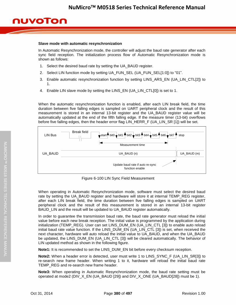
NuMicro M0518 Series Technical Reference Manual
Oct 31, 2014 Page 380 of 497 Revision 1.00
NU
MIC
RO
™ M
0518
SE
RIE
S T
EC
HN
ICA
L R
EF
ER
EN
CE
MA
NU
AL
Slave mode with automatic resynchronization
In Automatic Resynchronization mode, the controller will adjust the baud rate generator after each sync field reception. The initialization process flow of Automatic Resynchronization mode is shown as follows:
1. Select the desired baud rate by setting the UA_BAUD register.
2. Select LIN function mode by setting UA_FUN_SEL (UA_FUN_SEL[1:0]) to “01”.
3. Enable automatic resynchronization function by setting LINS_ARS_EN (UA_LIN_CTL[2]) to 1.
4. Enable LIN slave mode by setting the LINS_EN (UA_LIN_CTL[0]) is set to 1.
When the automatic resynchronization function is enabled, after each LIN break field, the time duration between five falling edges is sampled on UART peripheral clock and the result of this measurement is stored in an internal 13-bit register and the UA_BAUD register value will be automatically updated at the end of the fifth falling edge. If the measure timer (13-bit) overflows before five falling edges, then the header error flag LIN_HERR_F (UA_LIN_SR [1]) will be set.
start bit0 bit1 bit2 bit3 bit4 bit5 bit6 bit7 stop
UA_BAUD (m)UA_BAUD (n)
Measurement time
Break fieldLIN Bus
UA_BAUD
Update baud rate if auto re-sync
function enable
Figure 6-100 LIN Sync Field Measurement
When operating in Automatic Resynchronization mode, software must select the desired baud rate by setting the UA_BAUD register and hardware will store it at internal TEMP_REG register, after each LIN break field, the time duration between five falling edges is sampled on UART peripheral clock and the result of this measurement is stored in an internal 13-bit register BAUD_LIN and the result will be updated to UA_BAUD register automatically.
In order to guarantee the transmission baud rate, the baud rate generator must reload the initial value before each new break reception. The initial value is programmed by the application during initialization (TEMP_REG). User can set LINS_DUM_EN (UA_LIN_CTL [3]) to enable auto reload initial baud rate value function. If the LINS_DUM_EN (UA_LIN_CTL [3]) is set, when received the next character, hardware will auto reload the initial value to UA_BAUD, and when the UA_BAUD be updated, the LINS_DUM_EN (UA_LIN_CTL [3]) will be cleared automatically. The behavior of LIN updated method as shown in the following figure.
Note1: It is recommended to set the LINS_DUM_EN bit before every checksum reception.
Note2: When a header error is detected, user must write 1 to LINS_SYNC_F (UA_LIN_SR[3]) to re-search new frame header. When writing 1 to it, hardware will reload the initial baud rate TEMP_REG and re-search new frame header.
Note3: When operating in Automatic Resynchronization mode, the baud rate setting must be operated at mode2 (DIV_X_EN (UA_BAUD [29]) and DIV_X_ONE (UA_BAUD[28]) must be 1).

NuMicro M0518 Series Technical Reference Manual
Oct 31, 2014 Page 381 of 497 Revision 1.00
NU
MIC
RO
™ M
0518
SE
RIE
S T
EC
HN
ICA
L R
EF
ER
EN
CE
MA
NU
AL
Data 1 Data 2 Data NCheck
Sum
Protected
Identifier
field
Response
Inter-
frame
space
Frame slot
Synch
fieldBreak
Field
Measurement
time
UA_BAUD (n) UA_BAUD (m) UA_BAUD (n)
S/W set LINS_DUM_EN to 1H/W auto-reload initial baud
rate which backup in
TEMP_REG and cleared
LINS_DUM_EN to 0 by H/W
update UA_BAUD register
(UA_BAUD = BAUD_LIN value)
TEMP_REG value is UA_BAUD(n)
BAUD_LIN value is UA_BAUD(m)
Both of TEMP_REG and BAUD_LIN are internal register
Figure 6-101 UA_BAUD Update Sequence in Automatic Resynchronization Mode when LINS_DUM_EN (UA_LIN_CTL[3]) = 1
Data 1 Data 2 Data NCheck
Sum
Protected
Identifier
field
Response
Inter-
frame
space
Frame slot
Synch
fieldBreak
Field
Measurement
time
UA_BAUD (n) UA_BAUD (m)
If LINS_DUM_EN value is 0,
H/W will not restore initial
baud rate to UA_BAUD
update UA_BAUD register
(UA_BAUD = BAUD_LIN value)
TEMP_REG value is UA_BAUD(n)
BAUD_LIN value is UA_BAUD(m)
Both of TEMP_REG and BAUD_LIN are internal register
Figure 6-102 UA_BAUD Update Sequence in Automatic Resynchronization Mode when LINS_DUM_EN (UA_LIN_CTL[3])= 0
NuMicro M0518 Series Technical Reference Manual
Oct 31, 2014 Page 382 of 497 Revision 1.00
NU
MIC
RO
™ M
0518
SE
RIE
S T
EC
HN
ICA
L R
EF
ER
EN
CE
MA
NU
AL
Deviation error on the sync field
When operating in Automatic Resynchronization mode, the controller will check the deviation error on the sync field. The deviation error is checked by comparing the current baud rate with the received sync field. Two checks are performed in parallel.
Check1: Based on measurement between the first falling edge and the last falling edge of the sync field.
If the difference is more than 14.84%, the header error flag LINS_HERR_F (UA_LIN_SR[1]) will be set.
If the difference is less than 14.06%, the header error flag LINS_HERR_F (UA_LIN_SR[1]) will not be set.
If the difference is between 14.84% and 14.06%, the header error flag LINS_HERR_F (UA_LIN_SR[1]) may either set or not.
Check2: Based on measurement of time between each falling edge of the sync field.
If the difference is more than 18.75%, the header error flag LINS_HERR_F (UA_LIN_SR[1]) will be set.
If the difference is less than 15.62%, the header error flag LINS_HERR_F (UA_LIN_SR[1]) will not be set.
If the difference is between 18.75% and 15.62%, the header error flag LINS_HERR_F (UA_LIN_SR[1]) may either set or not.
Note: The deviation check is based on the current baud rate clock. Therefore, in order to guarantee correct deviation checking, the baud rate must reload the nominal value before each new break reception by setting LINS_DUM_EN (UA_LIN_CTL[3]) register (It is recommend setting the LINS_DUM_EN (UA_LIN_CTL[3]) bit before every checksum reception).
LIN header error detection
In LIN Slave function mode, when user enables the header detection function by setting the LINS_HDET_EN (UA_LIN_CTL[1]), hardware will handle the header detect flow. If the header has an error, the LIN header error flag LIN_HERR_F (UA_LIN_SR[1]) will be set and an interrupt is generated if the LIN_IEN (UA_IER[8]) bit is set. When header error is detected, user must reset the detect circuit to re-search a new frame header by writing 1 to LINS_SYNC_F (UA_LIN_SR[3]) to re-search a new frame header.
The LIN header error flag LIN_HERR_F (UA_LIN_SR[1]) is set if one of the following conditions occurs:
Break Delimiter is too short (less than 0.5-bit time).
Frame error in sync field or Identifier field.
The sync field data is not 0x55 (Non-Automatic Resynchronization mode).
The sync field deviation error (With Automatic Resynchronization mode).
The sync field measure time-out (With Automatic Resynchronization mode).
LIN header reception time-out.

NuMicro M0518 Series Technical Reference Manual
Oct 31, 2014 Page 383 of 497 Revision 1.00
NU
MIC
RO
™ M
0518
SE
RIE
S T
EC
HN
ICA
L R
EF
ER
EN
CE
MA
NU
AL
6.11.5.9 RS-485 Function Mode
Another alternate function of UART Controller is RS-485 function (user must set UA_FUN_SEL [1:0] to “11” to enable RS-485 function), and direction control provided by RTS pin from an asynchronous serial port. The RS-485 transceiver control is implemented by using the RTS control signal to enable the RS-485 driver. Many characteristics of the RX and TX are same as UART in RS-485 mode.
The UART controller can be configured as an RS-485 addressable slave and the RS-485 master transmitter will identify an address character by setting the parity (9-th bit) to 1. For data characters, the parity is set to 0. Software can use UA_LCR register to control the 9-th bit (When the PBE(UA_LCR[3]), EPE(UA_LCR[4]) and SPE(UA_LCR[5]) are set, the 9-th bit is transmitted 0 and when PBE and SPE are set and EPE is cleared, the 9-th bit is transmitted 1).
The controller supports three operation modes: RS-485 Normal Multidrop Operation Mode (NMM), RS-485 Auto Address Detection Operation Mode (AAD) and RS-485 Auto Direction Control Operation Mode (AUD). Software can choose any operation mode by programming the UA_ALT_CSR register, and drive the transfer delay time between the last stop bit leaving the TX FIFO and the de-assertion of by setting DLY (UA_TOR [15:8]) register.
6.11.5.9.1 RS-485 Normal Multidrop Operation Mode (NMM)
In RS-485 Normal Multidrop Operation Mode (RS485_NMM(UA_ALT_CSR[8]) = 1), in first, software must decide the data which before the address byte be detected will be stored in RX FIFO or not. If software wants to ignore any data before address byte detected, the flow is set RX_DIS (UA_FCR [8]) then enable RS485_NMM (UA_ALT_CSR [8]) and the receiver will ignore any data until an address byte is detected (bit 9 = 1) and the address byte data will be stored in the RX FIFO. If software wants to receive any data before address byte detected, the flow is disables RX_DIS (UA_FCR [8]) then enable RS485_NMM (UA_ALT_CSR [8]) and the receiver will received any data.
If an address byte is detected (bit 9 = 1), it will generate an interrupt to CPU and RX_DIS (UA_FCR [8]) can decide whether accepting the following data bytes are stored in the RX FIFO. If software disables receiver by setting RX_DIS (UA_FCR [8]) register, when a next address byte is detected, the controller will clear the RX_DIS (UA_FCR [8]) bit and the address byte data will be stored in the RX FIFO.
6.11.5.9.2 RS-485 Auto Address Detection Operation Mode (AAD)
In RS-485 Auto Address Detection Operation Mode (RS485_AAD(UA_ALT_CSR[9]) = 1), the receiver will ignore any data until an address byte is detected (bit 9 = 1) and the address byte data matches the ADDR_MATCH (UA_ALT_CSR[31:24]) value. The address byte data will be stored in the RX FIFO. The all received byte data will be accepted and stored in the RX FIFO until an address byte data not match the ADDR_MATCH (UA_ALT_CSR[31:24]) value.
6.11.5.9.3 RS-485 Auto Direction Mode (AUD)
Another option function of RS-485 controllers is RS-485 auto direction control function (RS485_AUD(UA_ALT_CSR[10) = 1). The RS-485 transceiver control is implemented by using the RTS control signal from an asynchronous serial port. The RTS line is connected to the RS-485 transceiver enable pin such that setting the RTS line to high (logic 1) enables the RS-485 transceiver. Setting the RTS line to low (logic 0) puts the transceiver into the tri-state condition to disabled. User can set LEV_RTS in UA_MCR register to change the RTS driving level.
The following diagram demonstrates the RS-485 RTS driving level in AUD mode. The RTS pin will be automatically driven during TX data transmission.
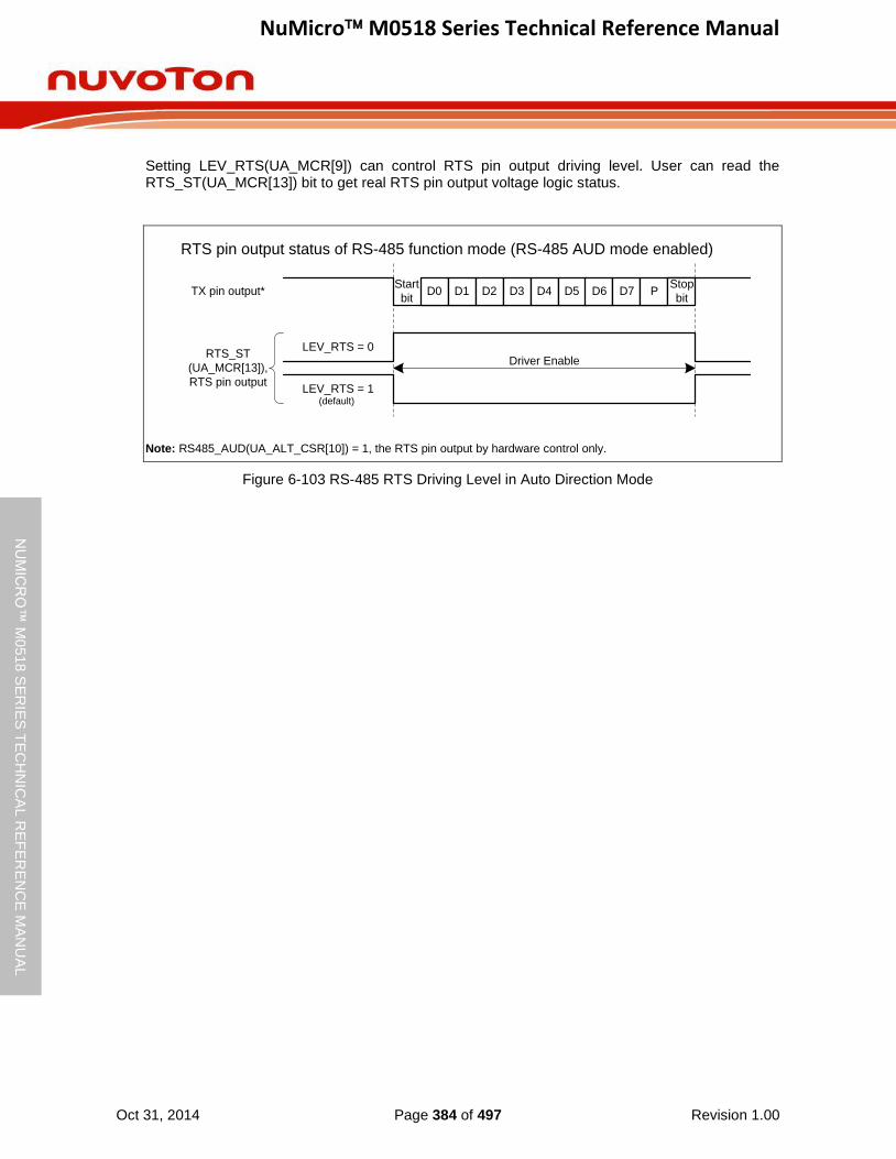
NuMicro M0518 Series Technical Reference Manual
Oct 31, 2014 Page 384 of 497 Revision 1.00
NU
MIC
RO
™ M
0518
SE
RIE
S T
EC
HN
ICA
L R
EF
ER
EN
CE
MA
NU
AL
Setting LEV_RTS(UA_MCR[9]) can control RTS pin output driving level. User can read the RTS_ST(UA_MCR[13]) bit to get real RTS pin output voltage logic status.
LEV_RTS = 0
LEV_RTS = 1
RTS pin output status of RS-485 function mode (RS-485 AUD mode enabled)
D0 D1 D2 D3 D4 D5 D6 D7 PStart
bit
Stop
bitTX pin output*
RTS_ST
(UA_MCR[13]),
RTS pin output
(default)
Driver Enable
Note: RS485_AUD(UA_ALT_CSR[10]) = 1, the RTS pin output by hardware control only.
Figure 6-103 RS-485 RTS Driving Level in Auto Direction Mode
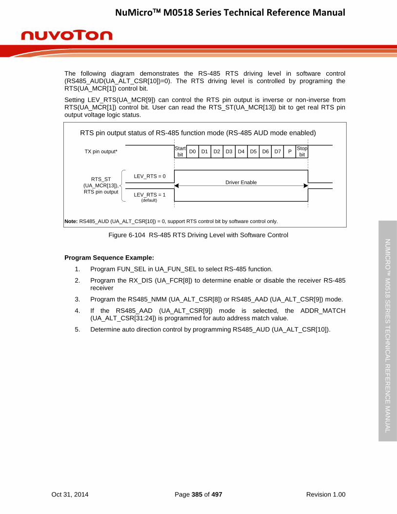
NuMicro M0518 Series Technical Reference Manual
Oct 31, 2014 Page 385 of 497 Revision 1.00
NU
MIC
RO
™ M
0518
SE
RIE
S T
EC
HN
ICA
L R
EF
ER
EN
CE
MA
NU
AL
The following diagram demonstrates the RS-485 RTS driving level in software control (RS485_AUD(UA_ALT_CSR[10])=0). The RTS driving level is controlled by programing the RTS(UA_MCR[1]) control bit.
Setting LEV_RTS(UA_MCR[9]) can control the RTS pin output is inverse or non-inverse from RTS(UA_MCR[1]) control bit. User can read the RTS_ST(UA_MCR[13]) bit to get real RTS pin output voltage logic status.
LEV_RTS = 0
LEV_RTS = 1
RTS pin output status of RS-485 function mode (RS-485 AUD mode enabled)
D0 D1 D2 D3 D4 D5 D6 D7 PStart
bit
Stop
bitTX pin output*
RTS_ST
(UA_MCR[13]),
RTS pin output
(default)
Driver Enable
Note: RS485_AUD (UA_ALT_CSR[10]) = 0, support RTS control bit by software control only.
Figure 6-104 RS-485 RTS Driving Level with Software Control
Program Sequence Example:
1. Program FUN_SEL in UA_FUN_SEL to select RS-485 function.
2. Program the RX_DIS (UA_FCR[8]) to determine enable or disable the receiver RS-485 receiver
3. Program the RS485_NMM (UA_ALT_CSR[8]) or RS485_AAD (UA_ALT_CSR[9]) mode.
4. If the RS485_AAD (UA_ALT_CSR[9]) mode is selected, the ADDR_MATCH (UA_ALT_CSR[31:24]) is programmed for auto address match value.
5. Determine auto direction control by programming RS485_AUD (UA_ALT_CSR[10]).

NuMicro M0518 Series Technical Reference Manual
Oct 31, 2014 Page 386 of 497 Revision 1.00
NU
MIC
RO
™ M
0518
SE
RIE
S T
EC
HN
ICA
L R
EF
ER
EN
CE
MA
NU
AL
Start
bitD0TX pin output
RTS_ST
(UA_MCR[13])Driver Enable*
RX
TX
RTS
Differential Bus
RS- 485 TransceiverUART / RS- 485 Controller
D1 D2 D3 D4 D5 D6 D7 PStop
bit
Driver Enable
Note: RS485_AUD(UA_ALT_CSR[10]) must be set to 1, and LEV_RTS(UA_MCR[9]) must be set to 0.
Figure 6-105 Structure of RS-485 Frame
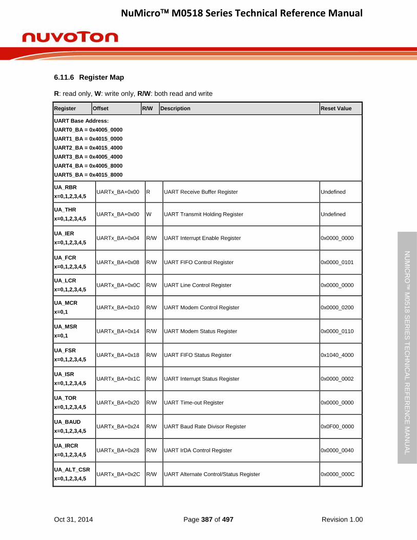
NuMicro M0518 Series Technical Reference Manual
Oct 31, 2014 Page 387 of 497 Revision 1.00
NU
MIC
RO
™ M
0518
SE
RIE
S T
EC
HN
ICA
L R
EF
ER
EN
CE
MA
NU
AL
6.11.6 Register Map
R: read only, W: write only, R/W: both read and write
Register Offset R/W Description Reset Value
UART Base Address:
UART0_BA = 0x4005_0000
UART1_BA = 0x4015_0000
UART2_BA = 0x4015_4000
UART3_BA = 0x4005_4000
UART4_BA = 0x4005_8000
UART5_BA = 0x4015_8000
UA_RBR
x=0,1,2,3,4,5 UARTx_BA+0x00 R UART Receive Buffer Register Undefined
UA_THR
x=0,1,2,3,4,5 UARTx_BA+0x00 W UART Transmit Holding Register Undefined
UA_IER
x=0,1,2,3,4,5 UARTx_BA+0x04 R/W UART Interrupt Enable Register 0x0000_0000
UA_FCR
x=0,1,2,3,4,5 UARTx_BA+0x08 R/W UART FIFO Control Register 0x0000_0101
UA_LCR
x=0,1,2,3,4,5 UARTx_BA+0x0C R/W UART Line Control Register 0x0000_0000
UA_MCR
x=0,1 UARTx_BA+0x10 R/W UART Modem Control Register 0x0000_0200
UA_MSR
x=0,1 UARTx_BA+0x14 R/W UART Modem Status Register 0x0000_0110
UA_FSR
x=0,1,2,3,4,5 UARTx_BA+0x18 R/W UART FIFO Status Register 0x1040_4000
UA_ISR
x=0,1,2,3,4,5 UARTx_BA+0x1C R/W UART Interrupt Status Register 0x0000_0002
UA_TOR
x=0,1,2,3,4,5 UARTx_BA+0x20 R/W UART Time-out Register 0x0000_0000
UA_BAUD
x=0,1,2,3,4,5 UARTx_BA+0x24 R/W UART Baud Rate Divisor Register 0x0F00_0000
UA_IRCR
x=0,1,2,3,4,5 UARTx_BA+0x28 R/W UART IrDA Control Register 0x0000_0040
UA_ALT_CSR
x=0,1,2,3,4,5 UARTx_BA+0x2C R/W UART Alternate Control/Status Register 0x0000_000C

NuMicro M0518 Series Technical Reference Manual
Oct 31, 2014 Page 388 of 497 Revision 1.00
NU
MIC
RO
™ M
0518
SE
RIE
S T
EC
HN
ICA
L R
EF
ER
EN
CE
MA
NU
AL
UA_FUN_SEL
x=0,1,2,3,4,5 UARTx_BA+0x30 R/W UART Function Select Register 0x0000_0000
UA_LIN_CTL
x=0,1,2 UARTx_BA+0x34 R/W UART LIN Control Register 0x000C_0000
UA_LIN_SR
x=0,1,2 UARTx_BA+0x38 R/W UART LIN Status Register 0x0000_0000
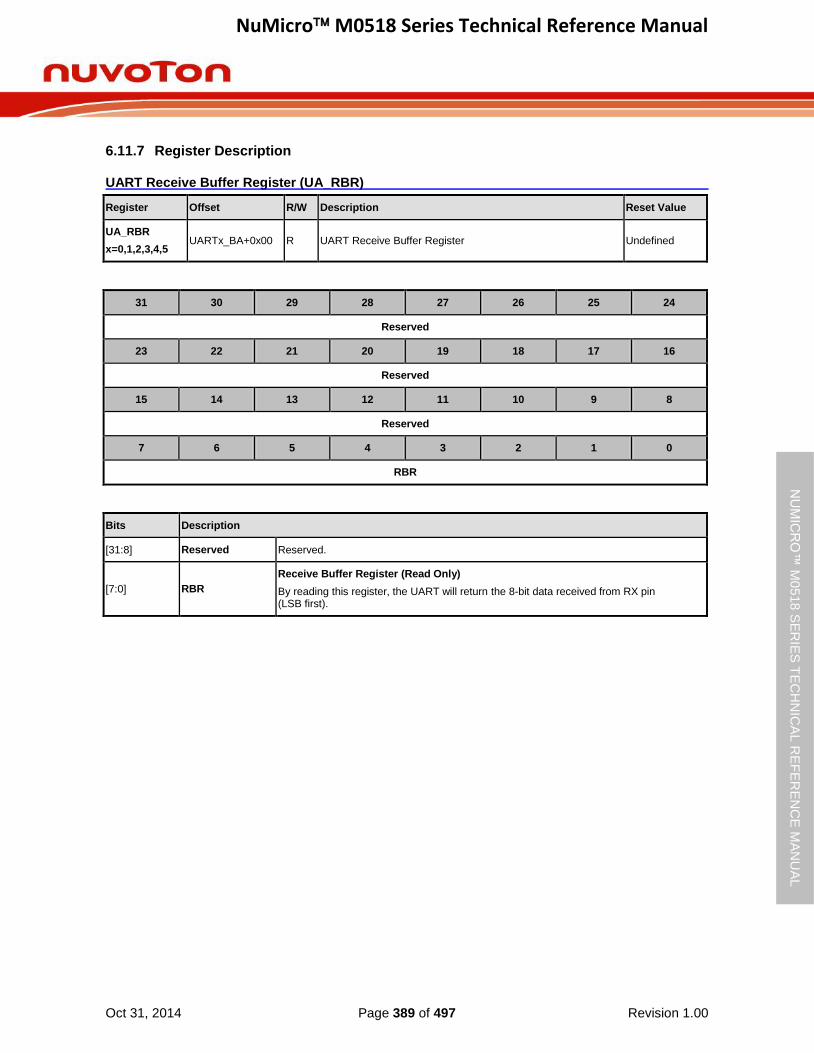
NuMicro M0518 Series Technical Reference Manual
Oct 31, 2014 Page 389 of 497 Revision 1.00
NU
MIC
RO
™ M
0518
SE
RIE
S T
EC
HN
ICA
L R
EF
ER
EN
CE
MA
NU
AL
6.11.7 Register Description
UART Receive Buffer Register (UA_RBR)
Register Offset R/W Description Reset Value
UA_RBR
x=0,1,2,3,4,5 UARTx_BA+0x00 R UART Receive Buffer Register Undefined
31 30 29 28 27 26 25 24
Reserved
23 22 21 20 19 18 17 16
Reserved
15 14 13 12 11 10 9 8
Reserved
7 6 5 4 3 2 1 0
RBR
Bits Description
[31:8] Reserved Reserved.
[7:0] RBR
Receive Buffer Register (Read Only)
By reading this register, the UART will return the 8-bit data received from RX pin (LSB first).
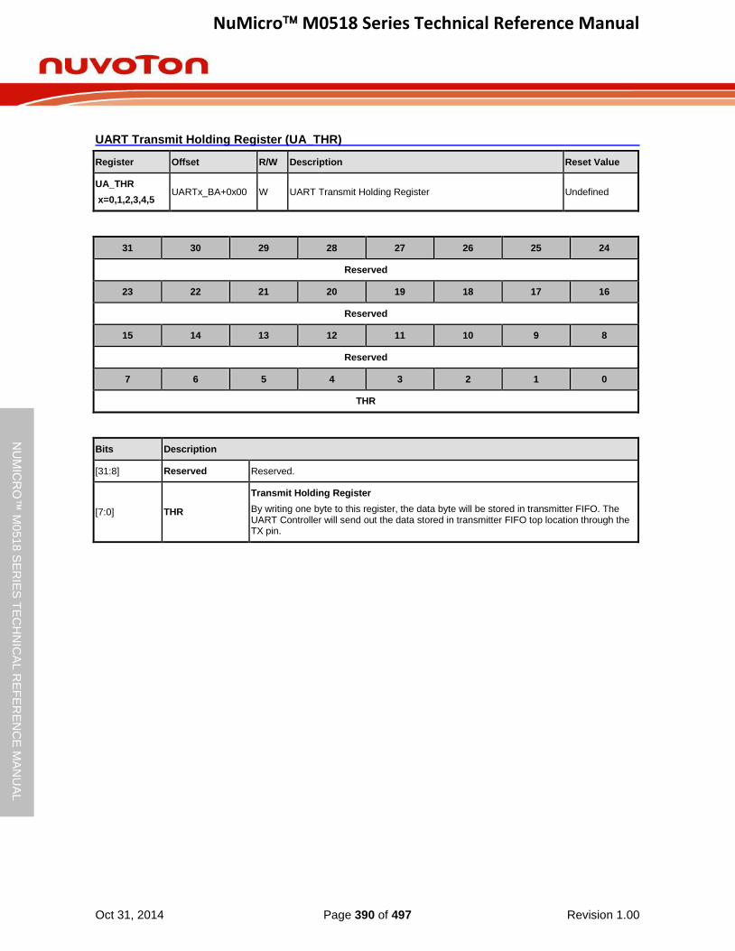
NuMicro M0518 Series Technical Reference Manual
Oct 31, 2014 Page 390 of 497 Revision 1.00
NU
MIC
RO
™ M
0518
SE
RIE
S T
EC
HN
ICA
L R
EF
ER
EN
CE
MA
NU
AL
UART Transmit Holding Register (UA_THR)
Register Offset R/W Description Reset Value
UA_THR
x=0,1,2,3,4,5 UARTx_BA+0x00 W UART Transmit Holding Register Undefined
31 30 29 28 27 26 25 24
Reserved
23 22 21 20 19 18 17 16
Reserved
15 14 13 12 11 10 9 8
Reserved
7 6 5 4 3 2 1 0
THR
Bits Description
[31:8] Reserved Reserved.
[7:0] THR
Transmit Holding Register
By writing one byte to this register, the data byte will be stored in transmitter FIFO. The UART Controller will send out the data stored in transmitter FIFO top location through the TX pin.

NuMicro M0518 Series Technical Reference Manual
Oct 31, 2014 Page 391 of 497 Revision 1.00
NU
MIC
RO
™ M
0518
SE
RIE
S T
EC
HN
ICA
L R
EF
ER
EN
CE
MA
NU
AL
UART Interrupt Enable Register (UA_IER)
Register Offset R/W Description Reset Value
UA_IER
x=0,1,2,3,4,5 UARTx_BA+0x04 R/W UART Interrupt Enable Register 0x0000_0000
31 30 29 28 27 26 25 24
Reserved
23 22 21 20 19 18 17 16
Reserved ABRIEN Reserved
15 14 13 12 11 10 9 8
Reserved AUTO_CTS_E
N AUTO_RTS_E
N TIME_OUT_E
N WKDATIEN Reserved LIN_IEN
7 6 5 4 3 2 1 0
Reserved WKCTSIEN BUF_ERR_IE
N TOUT_IEN MODEM_IEN RLS_IEN THRE_IEN RDA_IEN
Bits Description
[31:19] Reserved Reserved.
[18] ABRIEN
Auto-Baud Rate Interrupt Enable Control
0 = Auto-baud rate interrupt Disabled.
1 = Auto-baud rate interrupt Enabled.
[17:14] Reserved Reserved.
[13] AUTO_CTS_EN
CTS Auto Flow Control Enable Coontrol (Available In UART0/UART1 Channel)
0 = CTS auto flow control Disabled.
1 = CTS auto flow control Enabled.
When CTS auto-flow is enabled, the UART will send data to external device when CTS input assert (UART will not send data to device until CTS is asserted).
[12] AUTO_RTS_EN
RTS Auto Flow Control Enable Coontrol ( Available In UART0/UART1 Channel)
0 = RTS auto flow control Disabled.
1 = RTS auto flow control Enabled.
When RTS auto-flow is enabled, if the number of bytes in the RX FIFO equals the RTS_TRI_LEV (UA_FCR [19:16]), the UART will de-assert RTS signal.
[11] TIME_OUT_EN
Time-Out Counter Enable Coontrol
0 = Time-out counter Disabled.
1 = Time-out counter Enabled.
[10] WKDATIEN
Incoming Data Wake-Up Interrupt Enable Control
0 = Incoming data wake-up system function Disabled.
1 = Incoming data wake-up system function Enabled, when the system is in Power-down mode, incoming data will wake-up system from Power-down mode.
Note: Hardware will clear this bit when the incoming data wake-up operation finishes and “system clock” work stable.
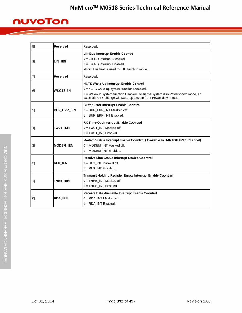
NuMicro M0518 Series Technical Reference Manual
Oct 31, 2014 Page 392 of 497 Revision 1.00
NU
MIC
RO
™ M
0518
SE
RIE
S T
EC
HN
ICA
L R
EF
ER
EN
CE
MA
NU
AL
[9] Reserved Reserved.
[8] LIN_IEN
LIN Bus Interrupt Enable Coontrol
0 = Lin bus interrupt Disabled.
1 = Lin bus interrupt Enabled.
Note: This field is used for LIN function mode.
[7] Reserved Reserved.
[6] WKCTSIEN
NCTS Wake-Up Interrupt Enable Control
0 = nCTS wake-up system function Disabled.
1 = Wake-up system function Enabled, when the system is in Power-down mode, an external nCTS change will wake-up system from Power-down mode.
[5] BUF_ERR_IEN
Buffer Error Interrupt Enable Coontrol
0 = BUF_ERR_INT Masked off.
1 = BUF_ERR_INT Enabled.
[4] TOUT_IEN
RX Time-Out Interrupt Enable Coontrol
0 = TOUT_INT Masked off.
1 = TOUT_INT Enabled.
[3] MODEM_IEN
Modem Status Interrupt Enable Coontrol (Available In UART0/UART1 Channel)
0 = MODEM_INT Masked off.
1 = MODEM_INT Enabled.
[2] RLS_IEN
Receive Line Status Interrupt Enable Coontrol
0 = RLS_INT Masked off.
1 = RLS_INT Enabled.
[1] THRE_IEN
Transmit Holding Register Empty Interrupt Enable Coontrol
0 = THRE_INT Masked off.
1 = THRE_INT Enabled.
[0] RDA_IEN
Receive Data Available Interrupt Enable Coontrol
0 = RDA_INT Masked off.
1 = RDA_INT Enabled.
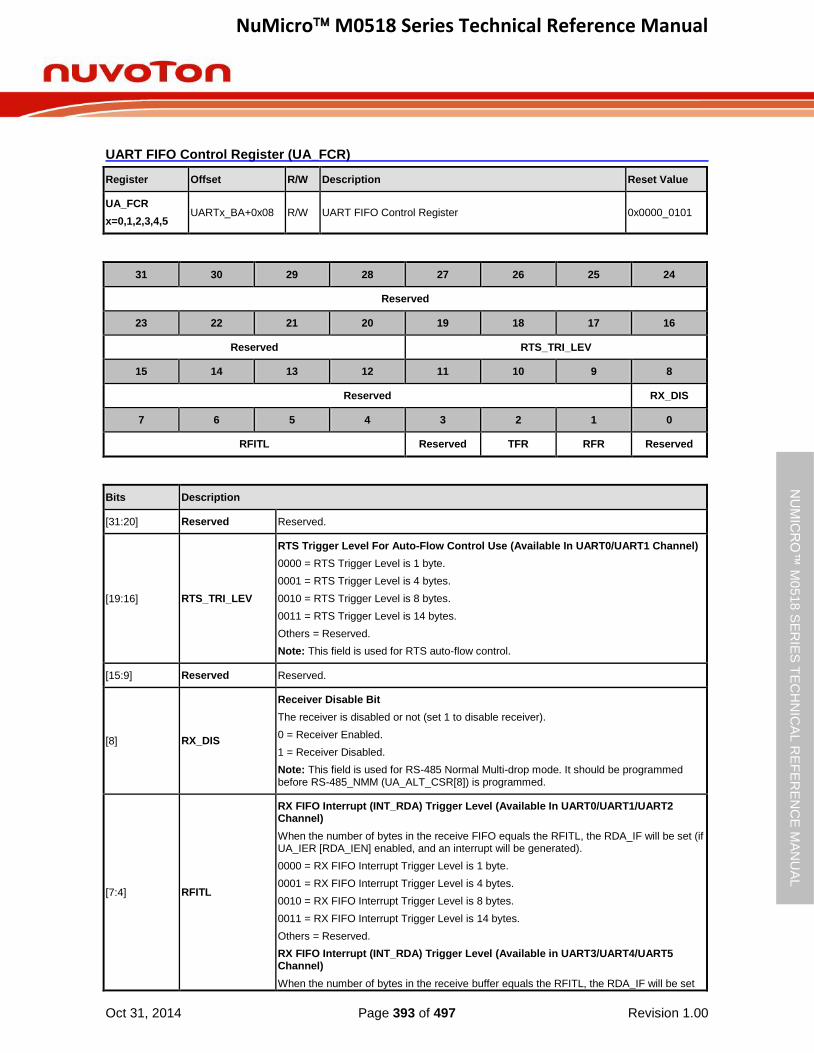
NuMicro M0518 Series Technical Reference Manual
Oct 31, 2014 Page 393 of 497 Revision 1.00
NU
MIC
RO
™ M
0518
SE
RIE
S T
EC
HN
ICA
L R
EF
ER
EN
CE
MA
NU
AL
UART FIFO Control Register (UA_FCR)
Register Offset R/W Description Reset Value
UA_FCR
x=0,1,2,3,4,5 UARTx_BA+0x08 R/W UART FIFO Control Register 0x0000_0101
31 30 29 28 27 26 25 24
Reserved
23 22 21 20 19 18 17 16
Reserved RTS_TRI_LEV
15 14 13 12 11 10 9 8
Reserved RX_DIS
7 6 5 4 3 2 1 0
RFITL Reserved TFR RFR Reserved
Bits Description
[31:20] Reserved Reserved.
[19:16] RTS_TRI_LEV
RTS Trigger Level For Auto-Flow Control Use (Available In UART0/UART1 Channel)
0000 = RTS Trigger Level is 1 byte.
0001 = RTS Trigger Level is 4 bytes.
0010 = RTS Trigger Level is 8 bytes.
0011 = RTS Trigger Level is 14 bytes.
Others = Reserved.
Note: This field is used for RTS auto-flow control.
[15:9] Reserved Reserved.
[8] RX_DIS
Receiver Disable Bit
The receiver is disabled or not (set 1 to disable receiver).
0 = Receiver Enabled.
1 = Receiver Disabled.
Note: This field is used for RS-485 Normal Multi-drop mode. It should be programmed before RS-485_NMM (UA_ALT_CSR[8]) is programmed.
[7:4] RFITL
RX FIFO Interrupt (INT_RDA) Trigger Level (Available In UART0/UART1/UART2 Channel)
When the number of bytes in the receive FIFO equals the RFITL, the RDA_IF will be set (if UA_IER [RDA_IEN] enabled, and an interrupt will be generated).
0000 = RX FIFO Interrupt Trigger Level is 1 byte.
0001 = RX FIFO Interrupt Trigger Level is 4 bytes.
0010 = RX FIFO Interrupt Trigger Level is 8 bytes.
0011 = RX FIFO Interrupt Trigger Level is 14 bytes.
Others = Reserved.
RX FIFO Interrupt (INT_RDA) Trigger Level (Available in UART3/UART4/UART5 Channel)
When the number of bytes in the receive buffer equals the RFITL, the RDA_IF will be set

NuMicro M0518 Series Technical Reference Manual
Oct 31, 2014 Page 394 of 497 Revision 1.00
NU
MIC
RO
™ M
0518
SE
RIE
S T
EC
HN
ICA
L R
EF
ER
EN
CE
MA
NU
AL
(if RDA_IEN (UA_IER[0]) enabled, and an interrupt will be generated). There is only one receive buffer in UART3/UART4/UART5.
0000 = RX Buffer Interrupt Trigger Level is 1 byte.
Others = Reserved.
[3] Reserved Reserved.
[2] TFR
TX Field Software Reset
When TFR is set, all the byte in the transmit FIFO/ transmit buffer and TX internal state machine are cleared.
0 = No effect.
1 = Reset the TX internal state machine and pointers.
Note: This bit will automatically clear at least 3 UART peripherial clock cycles.
[1] RFR
RX Field Software Reset
When RFR is set, all the byte in the receiver FIFO /receive buffer and RX internal state machine are cleared.
0 = No effect.
1 = Reset the RX internal state machine and pointers.
Note: This bit will automatically clear at least 3 UART peripherial clock cycles.
[0] Reserved Reserved.
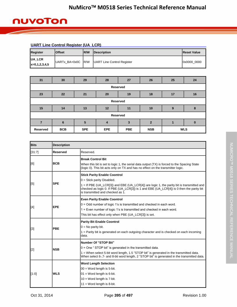
NuMicro M0518 Series Technical Reference Manual
Oct 31, 2014 Page 395 of 497 Revision 1.00
NU
MIC
RO
™ M
0518
SE
RIE
S T
EC
HN
ICA
L R
EF
ER
EN
CE
MA
NU
AL
UART Line Control Register (UA_LCR)
Register Offset R/W Description Reset Value
UA_LCR
x=0,1,2,3,4,5 UARTx_BA+0x0C R/W UART Line Control Register 0x0000_0000
31 30 29 28 27 26 25 24
Reserved
23 22 21 20 19 18 17 16
Reserved
15 14 13 12 11 10 9 8
Reserved
7 6 5 4 3 2 1 0
Reserved BCB SPE EPE PBE NSB WLS
Bits Description
[31:7] Reserved Reserved.
[6] BCB
Break Control Bit
When this bit is set to logic 1, the serial data output (TX) is forced to the Spacing State (logic 0). This bit acts only on TX and has no effect on the transmitter logic.
[5] SPE
Stick Parity Enable Coontrol
0 = Stick parity Disabled.
1 = If PBE (UA_LCR[3]) and EBE (UA_LCR[4]) are logic 1, the parity bit is transmitted and checked as logic 0. If PBE (UA_LCR[3]) is 1 and EBE (UA_LCR[4]) is 0 then the parity bit is transmitted and checked as 1.
[4] EPE
Even Parity Enable Coontrol
0 = Odd number of logic 1’s is transmitted and checked in each word.
1 = Even number of logic 1’s is transmitted and checked in each word.
This bit has effect only when PBE (UA_LCR[3]) is set.
[3] PBE
Parity Bit Enable Coontrol
0 = No parity bit.
1 = Parity bit is generated on each outgoing character and is checked on each incoming data.
[2] NSB
Number Of “STOP Bit”
0 = One “ STOP bit” is generated in the transmitted data.
1 = When select 5-bit word length, 1.5 “STOP bit” is generated in the transmitted data. When select 6-,7- and 8-bti word length, 2 “STOP bit” is generated in the transmitted data.
[1:0] WLS
Word Length Selection
00 = Word length is 5-bit.
01 = Word length is 6-bit.
10 = Word length is 7-bit.
11 = Word length is 8-bit.

NuMicro M0518 Series Technical Reference Manual
Oct 31, 2014 Page 396 of 497 Revision 1.00
NU
MIC
RO
™ M
0518
SE
RIE
S T
EC
HN
ICA
L R
EF
ER
EN
CE
MA
NU
AL
UART MODEM Control Register (UA_MCR) ( Available in UART0/UART1 Channel)
Register Offset R/W Description Reset Value
UA_MCR
x=0,1 UARTx_BA+0x10 R/W UART Modem Control Register 0x0000_0200
31 30 29 28 27 26 25 24
Reserved
23 22 21 20 19 18 17 16
Reserved
15 14 13 12 11 10 9 8
Reserved RTS_ST Reserved LEV_RTS Reserved
7 6 5 4 3 2 1 0
Reserved RTS Reserved
Bits Description
[31:14] Reserved Reserved.
[13] RTS_ST
RTS Pin State (Read Only) ( Available In UART0/UART1 Channel)
This bit mirror from RTS pin output of voltage logic status.
0 = RTS pin output is low level voltage logic state.
1 = RTS pin output is high level voltage logic state.
[12:10] Reserved Reserved.
[9] LEV_RTS
RTS Pin Active Level ( Available In UART0/UART1 Channel)
This bit defines the active level state of RTS pin output.
0 = RTS pin output is high level active.
1 = RTS pin output is low level active.
Note1: Refer to Figure 6-92 and Figure 6-93 for UART function mode.
Note2: Refer to Figure 6-103 and Figure 6-104 for RS-485 function mode.
[8:2] Reserved Reserved.
[1] RTS
RTS (Request-To-Send) Signal Control (Available In UART0/UART1 Channel)
This bit is direct control internal RTS signal active or not, and then drive the RTS pin output with LEV_RTS bit configuration.
0 = RTS signal is active.
1 = RTS signal is inactive.
Note1: This RTS signal control bit is not effective when RTS auto-flow control is enabled in UART function mode.
Note2: This RTS signal control bit is not effective when RS-485 auto direction mode (AUD) is enabled in RS-485 function mode.
[0] Reserved Reserved.

NuMicro M0518 Series Technical Reference Manual
Oct 31, 2014 Page 397 of 497 Revision 1.00
NU
MIC
RO
™ M
0518
SE
RIE
S T
EC
HN
ICA
L R
EF
ER
EN
CE
MA
NU
AL
UART Modem Status Register (UA_MSR) ( Available in UART0/UART1 Channel)
Register Offset R/W Description Reset Value
UA_MSR
x=0,1 UARTx_BA+0x14 R/W UART Modem Status Register 0x0000_0110
31 30 29 28 27 26 25 24
Reserved
23 22 21 20 19 18 17 16
Reserved
15 14 13 12 11 10 9 8
Reserved LEV_CTS
7 6 5 4 3 2 1 0
Reserved CTS_ST Reserved DCTSF
Bits Description
[31:9] Reserved Reserved.
[8] LEV_CTS
CTS Pin Active Level
This bit defines the active level state of CTS pin input.
0 = CTS pin input is high level active.
1 = CTS pin input is low level active.
Note: Refer to Figure 6-91 for more information.
[7:5] Reserved Reserved.
[4] CTS_ST
CTS Pin Status (Read Only)
This bit mirror from CTS pin input of voltage logic status.
0 = CTS pin input is low level voltage logic state.
1 = CTS pin input is high level voltage logic state.
Note: This bit echoes when UART Controller peripheral clock is enabled, and CTS multi-function port is selected.
[3:1] Reserved Reserved.
[0] DCTSF
Detect CTS State Change Flag (Read Only)
This bit is set whenever CTS input has change state, and it will generate Modem interrupt to CPU when MODEM_IEN (UA_IER [3]) is set to 1.
0 = CTS input has not change state.
1 = CTS input has change state.
Note: This bit is read only, but can be cleared by writing “1” to it.
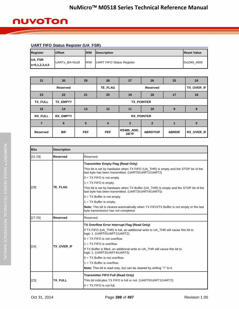
NuMicro M0518 Series Technical Reference Manual
Oct 31, 2014 Page 398 of 497 Revision 1.00
NU
MIC
RO
™ M
0518
SE
RIE
S T
EC
HN
ICA
L R
EF
ER
EN
CE
MA
NU
AL
UART FIFO Status Register (UA_FSR)
Register Offset R/W Description Reset Value
UA_FSR
x=0,1,2,3,4,5 UARTx_BA+0x18 R/W UART FIFO Status Register 0x1040_4000
31 30 29 28 27 26 25 24
Reserved TE_FLAG Reserved TX_OVER_IF
23 22 21 20 19 18 17 16
TX_FULL TX_EMPTY TX_POINTER
15 14 13 12 11 10 9 8
RX_FULL RX_EMPTY RX_POINTER
7 6 5 4 3 2 1 0
Reserved BIF FEF PEF RS485_ADD_
DETF ABRDTOIF ABRDIF RX_OVER_IF
Bits Description
[31:29] Reserved Reserved.
[28] TE_FLAG
Transmitter Empty Flag (Read Only)
This bit is set by hardware when TX FIFO (UA_THR) is empty and the STOP bit of the last byte has been transmitted. (UART0/UART1/UART2)
0 = TX FIFO is not empty.
1 = TX FIFO is empty.
This bit is set by hardware when TX Buffer (UA_THR) is empty and the STOP bit of the last byte has been transmitted. (UART3/UART4/UART5)
0 = TX Buffer is not empty.
1 = TX Buffer is empty.
Note: This bit is cleared automatically when TX FIFO/TX Buffer is not empty or the last byte transmission has not completed.
[27:25] Reserved Reserved.
[24] TX_OVER_IF
TX Overflow Error Interrupt Flag (Read Only)
If TX FIFO (UA_THR) is full, an additional write to UA_THR will cause this bit to logic 1. (UART0/UART1/UART2)
0 = TX FIFO is not overflow.
1 = TX FIFO is overflow.
If TX Buffer is filled, an additional write to UA_THR will cause this bit to logic 1. (UART3/UART4/UART5)
0 = TX Buffer is not overflow.
1 = TX Buffer is overflow.
Note: This bit is read only, but can be cleared by writing “1” to it.
[23] TX_FULL
Transmitter FIFO Full (Read Only)
This bit indicates TX FIFO is full or not. (UART0/UART1/UART2)
0 = TX FIFO is not full.
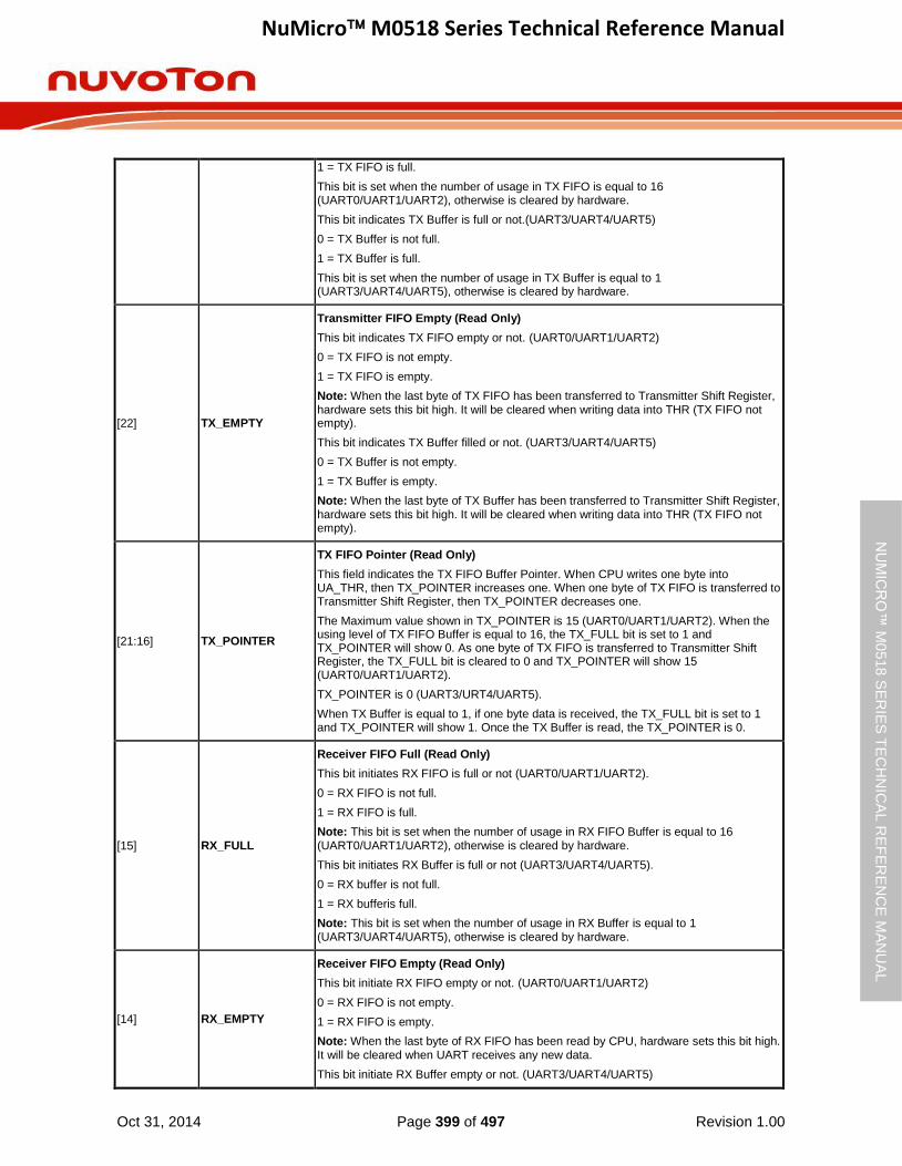
NuMicro M0518 Series Technical Reference Manual
Oct 31, 2014 Page 399 of 497 Revision 1.00
NU
MIC
RO
™ M
0518
SE
RIE
S T
EC
HN
ICA
L R
EF
ER
EN
CE
MA
NU
AL
1 = TX FIFO is full.
This bit is set when the number of usage in TX FIFO is equal to 16 (UART0/UART1/UART2), otherwise is cleared by hardware.
This bit indicates TX Buffer is full or not.(UART3/UART4/UART5)
0 = TX Buffer is not full.
1 = TX Buffer is full.
This bit is set when the number of usage in TX Buffer is equal to 1 (UART3/UART4/UART5), otherwise is cleared by hardware.
[22] TX_EMPTY
Transmitter FIFO Empty (Read Only)
This bit indicates TX FIFO empty or not. (UART0/UART1/UART2)
0 = TX FIFO is not empty.
1 = TX FIFO is empty.
Note: When the last byte of TX FIFO has been transferred to Transmitter Shift Register, hardware sets this bit high. It will be cleared when writing data into THR (TX FIFO not empty).
This bit indicates TX Buffer filled or not. (UART3/UART4/UART5)
0 = TX Buffer is not empty.
1 = TX Buffer is empty.
Note: When the last byte of TX Buffer has been transferred to Transmitter Shift Register, hardware sets this bit high. It will be cleared when writing data into THR (TX FIFO not empty).
[21:16] TX_POINTER
TX FIFO Pointer (Read Only)
This field indicates the TX FIFO Buffer Pointer. When CPU writes one byte into UA_THR, then TX_POINTER increases one. When one byte of TX FIFO is transferred to Transmitter Shift Register, then TX_POINTER decreases one.
The Maximum value shown in TX_POINTER is 15 (UART0/UART1/UART2). When the using level of TX FIFO Buffer is equal to 16, the TX_FULL bit is set to 1 and TX_POINTER will show 0. As one byte of TX FIFO is transferred to Transmitter Shift Register, the TX_FULL bit is cleared to 0 and TX_POINTER will show 15 (UART0/UART1/UART2).
TX_POINTER is 0 (UART3/URT4/UART5).
When TX Buffer is equal to 1, if one byte data is received, the TX_FULL bit is set to 1 and TX_POINTER will show 1. Once the TX Buffer is read, the TX_POINTER is 0.
[15] RX_FULL
Receiver FIFO Full (Read Only)
This bit initiates RX FIFO is full or not (UART0/UART1/UART2).
0 = RX FIFO is not full.
1 = RX FIFO is full.
Note: This bit is set when the number of usage in RX FIFO Buffer is equal to 16 (UART0/UART1/UART2), otherwise is cleared by hardware.
This bit initiates RX Buffer is full or not (UART3/UART4/UART5).
0 = RX buffer is not full.
1 = RX bufferis full.
Note: This bit is set when the number of usage in RX Buffer is equal to 1 (UART3/UART4/UART5), otherwise is cleared by hardware.
[14] RX_EMPTY
Receiver FIFO Empty (Read Only)
This bit initiate RX FIFO empty or not. (UART0/UART1/UART2)
0 = RX FIFO is not empty.
1 = RX FIFO is empty.
Note: When the last byte of RX FIFO has been read by CPU, hardware sets this bit high. It will be cleared when UART receives any new data.
This bit initiate RX Buffer empty or not. (UART3/UART4/UART5)

NuMicro M0518 Series Technical Reference Manual
Oct 31, 2014 Page 400 of 497 Revision 1.00
NU
MIC
RO
™ M
0518
SE
RIE
S T
EC
HN
ICA
L R
EF
ER
EN
CE
MA
NU
AL
0 = RX Buffer is not empty.
1 = RX Buffer is empty.
Note: When the last byte of RX Buffer has been read by CPU, hardware sets this bit high. It will be cleared when UART receives any new data.
[13:8] RX_POINTER
RX FIFO Pointer (Read Only)
This field indicates the RX FIFO Buffer Pointer. When UART receives one byte from external device, then RX_POINTER increases one. When one byte of RX FIFO is read by CPU, then RX_POINTER decreases one.
The Maximum value shown in RX_POINTER is 15 (UART0/UART1/UART2). When the using level of RX FIFO Buffer equal to 16, the RX_FULL bit is set to 1 and RX_POINTER will show 0. As one byte of RX FIFO is read by CPU, the RX_FULL bit is cleared to 0 and RX_POINTER will show 15 (UART0/UART1/UART2).
When RX Buffer is equal to 1, if one byte data is received, the RX_FULL bit is set to 1 and RX_POINTER will show 1. Once the RX Buffer is read, the RX_POINTER is 0.
[7] Reserved Reserved.
[6] BIF
Break Interrupt Flag (Read Only)
This bit is set to logic 1 whenever the received data input(RX) is held in the “spacing state” (logic 0) for longer than a full word transmission time (that is, the total time of “start bit” + data bits + parity + stop bits) and is reset whenever the CPU writes 1 to this bit.
0 = No Break interrupt is generated.
1 = Break interrupt is generated.
Note: This bit is read only, but can be cleared by writing “1” to it.
[5] FEF
Framing Error Flag (Read Only)
This bit is set to logic 1 whenever the received character does not have a valid “stop bit” (that is, the stop bit following the last data bit or parity bit is detected as logic 0), and is reset whenever the CPU writes 1 to this bit.
0 = No framing error is generated.
1 = Framing error is generated.
Note: This bit is read only, but can be cleared by writing “1” to it.
[4] PEF
Parity Error Flag (Read Only)
This bit is set to logic 1 whenever the received character does not have a valid “parity bit”, and is reset whenever the CPU writes 1 to this bit.
0 = No parity error is generated.
1 = Parity error is generated.
Note: This bit is read only, but can be cleared by writing “1” to it.
[3] RS485_ADD_DETF
RS-485 Address Byte Detection Flag (Read Only) (Available In UART0/UART1)
0 = Receiver detects a data that is not an address bit (bit 9 =’1’).
1 = Receiver detects a data that is an address bit (bit 9 =’1’).
Note1: This field is used for RS-485 function mode and RS485_ADD_EN (UA_ALT_CSR[15]) is set to 1 to enable Address detection mode.
Note2: This bit is read only, but can be cleared by writing ‘1’ to it.
[2] ABRDTOIF
Auto-Baud Rate Time-Out Interrupt (Read Only)
0 = Auto-baud rate counter is underflow.
1 = Auto-baud rate counter is overflow.
Note1: This bit is set to logic “1” in Auto-baud Rate Detect mode and the baud rate counter is overflow.
Note2: This bit is read only, but can be cleared by writing “1” to it.
[1] ABRDIF Auto-Baud Rate Detect Interrupt (Read Only)
0 = Auto-baud rate detect function is not finished.
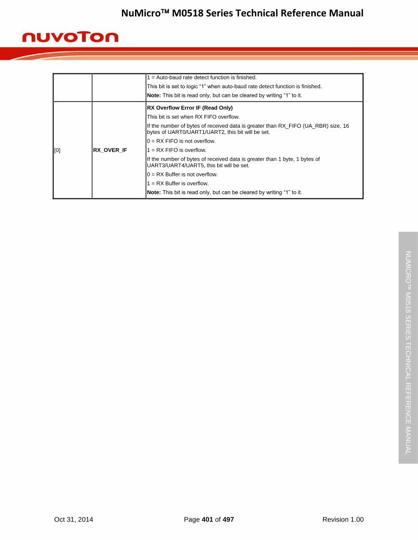
NuMicro M0518 Series Technical Reference Manual
Oct 31, 2014 Page 401 of 497 Revision 1.00
NU
MIC
RO
™ M
0518
SE
RIE
S T
EC
HN
ICA
L R
EF
ER
EN
CE
MA
NU
AL
1 = Auto-baud rate detect function is finished.
This bit is set to logic “1” when auto-baud rate detect function is finished.
Note: This bit is read only, but can be cleared by writing “1” to it.
[0] RX_OVER_IF
RX Overflow Error IF (Read Only)
This bit is set when RX FIFO overflow.
If the number of bytes of received data is greater than RX_FIFO (UA_RBR) size, 16 bytes of UART0/UART1/UART2, this bit will be set.
0 = RX FIFO is not overflow.
1 = RX FIFO is overflow.
If the number of bytes of received data is greater than 1 byte, 1 bytes of UART3/UART4/UART5, this bit will be set.
0 = RX Buffer is not overflow.
1 = RX Buffer is overflow.
Note: This bit is read only, but can be cleared by writing “1” to it.

NuMicro M0518 Series Technical Reference Manual
Oct 31, 2014 Page 402 of 497 Revision 1.00
NU
MIC
RO
™ M
0518
SE
RIE
S T
EC
HN
ICA
L R
EF
ER
EN
CE
MA
NU
AL
UART Interrupt Status Control Register (UA_ISR)
Register Offset R/W Description Reset Value
UA_ISR
x=0,1,2,3,4,5 UARTx_BA+0x1C R/W UART Interrupt Status Register 0x0000_0002
31 30 29 28 27 26 25 24
Reserved
23 22 21 20 19 18 17 16
Reserved DATWKIF CTSWKIF
15 14 13 12 11 10 9 8
LIN_INT Reserved BUF_ERR_IN
T TOUT_INT MODEM_INT RLS_INT THRE_INT RDA_INT
7 6 5 4 3 2 1 0
LIN_IF WKIF BUF_ERR_IF TOUT_IF MODEM_IF RLS_IF THRE_IF RDA_IF
Bits Description
[31:18] Reserved Reserved.
[17] DATWKIF
Data Wake-Up Interrupt Flag (Read Only)
This bit is set if chip wake-up from power-down state by data wake-up.
0 = Chip stays in power-down state.
1 = Chip wake-up from power-down state by data wake-up.
Note1: If WKDATIEN (UA_IER[10]) is enabled, the wake-up interrupt is generated.
Note2: This bit is read only, but can be cleared by writing ‘1’ to it.
[16] CTSWKIF
NCTS Wake-Up Interrupt Flag (Read Only)
0 = Chip stays in power-down state.
1 = Chip wake-up from power-down state by nCTS wake-up.
Note1: If WKCTSIEN (UA_IER[6])is enabled, the wake-up interrupt is generated.
Note2: This bit is read only, but can be cleared by writing ‘1’ to it.
[15] LIN_INT
LIN Bus Interrupt Indicator (Read Only)
This bit is set if LIN_IEN (UA_IER[8]) and LIN _IF(UA_ISR[7]) are both set to 1.
0 = No LIN Bus interrupt is generated.
1 = The LIN Bus interrupt is generated.
[14] Reserved Reserved.
[13] BUF_ERR_INT
Buffer Error Interrupt Indicator (Read Only)
This bit is set if BUF_ERR_IEN(UA_IER[5] and BUF_ERR_IF(UA_ISR[5]) are both set to 1.
0 = No buffer error interrupt is generated.
1 = Buffer error interrupt is generated.
[12] TOUT_INT Time-Out Interrupt Indicator (Read Only)
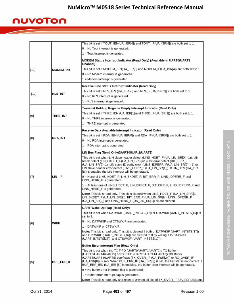
NuMicro M0518 Series Technical Reference Manual
Oct 31, 2014 Page 403 of 497 Revision 1.00
NU
MIC
RO
™ M
0518
SE
RIE
S T
EC
HN
ICA
L R
EF
ER
EN
CE
MA
NU
AL
This bit is set if TOUT_IEN(UA_IER[4]) and TOUT_IF(UA_ISR[4]) are both set to 1.
0 = No Tout interrupt is generated.
1 = Tout interrupt is generated.
[11] MODEM_INT
MODEM Status Interrupt Indicator (Read Only) (Available In UART0/UART1 Channel)
This bit is set if MODEM_IEN(UA_IER[3] and MODEM_IF(UA_ISR[4]) are both set to 1
0 = No Modem interrupt is generated.
1 = Modem interrupt is generated.
[10] RLS_INT
Receive Line Status Interrupt Indicator (Read Only)
This bit is set if RLS_IEN (UA_IER[2]) and RLS_IF(UA_ISR[2]) are both set to 1.
0 = No RLS interrupt is generated.
1 = RLS interrupt is generated.
[9] THRE_INT
Transmit Holding Register Empty Interrupt Indicator (Read Only)
This bit is set if THRE_IEN (UA_IER[1])and THRE_IF(UA_SR[1]) are both set to 1.
0 = No THRE interrupt is generated.
1 = THRE interrupt is generated.
[8] RDA_INT
Receive Data Available Interrupt Indicator (Read Only)
This bit is set if RDA_IEN (UA_IER[0]) and RDA_IF (UA_ISR[0]) are both set to 1.
0 = No RDA interrupt is generated.
1 = RDA interrupt is generated.
[7] LIN_ IF
LIN Bus Flag (Read Only)(UART0/UARt1/UART2)
This bit is set when LIN slave header detect (LINS_HDET_F (UA_LIN_SR[0] =1)), LIN break detect (LIN_BKDET_F(UA_LIN_SR[9]=1)), bit error detect (BIT_ERR_F (UA_LIN_SR[9]=1), LIN slave ID parity error (LINS_IDPERR_F(UA_LIN_SR[2] = 1) or LIN slave header error detect (LINS_HERR_F (UA_LIN_SR[1])). If LIN_ IEN (UA_IER [8]) is enabled the LIN interrupt will be generated.
0 = None of LINS_HDET_F, LIN_BKDET_F, BIT_ERR_F, LINS_IDPERR_F and LINS_HERR_F is generated.
1 = At least one of LINS_HDET_F, LIN_BKDET_F, BIT_ERR_F, LINS_IDPERR_F and LINS_HERR_F is generated.
Note: This bit is read only. This bit is cleared when LINS_HDET_F (UA_LIN_SR[0]), LIN_BKDET_F (UA_LIN_SR[9]), BIT_ERR_F (UA_LIN_SR[9]), LINS_IDPENR_F (UA_LIN_SR[2]) and LINS_HERR_F (UA_LIN_SR[1]) all are cleared.
[6] WKIF
UART Wake-Up Flag (Read Only)
This bit is set when DATWKIF (UART_INTSTS[17]) or CTSWKIF(UART_INTSTS[16]) is set to 1.
0 = No DATWKIF and CTSWKIF are generated.
1 = DATWKIF or CTSWKIF.
Note: This bit is read only. This bit is cleared if both of DATWKIF (UART_INTSTS[17]) and CTSWKIF (UART_INTSTS[16]) are cleared to 0 by writing 1 to DATWKIF (UART_INTSTS[17]) and CTSWKIF (UART_INTSTS[17]).
[5] BUF_ERR_IF
Buffer Error Interrupt Flag (Read Only)
This bit is set when the TX FIFO (UART0/UART1/UART2) / TX Buffer (UART3/UART4/UART5) or RX FIFO (UART0/UART1/UART2)/ RX Buffer (UART3/UART4/UART5) overflows (TX_OVER_IF (UA_FSR[24]) or RX_OVER_IF (UA_FSR[0]) is set). When BUF_ERR_IF (UA_ISR[5]) is set, the transfer is not correct. If BUF_ERR_IEN (UA_IER [8]) is enabled, the buffer error interrupt will be generated.
0 = No buffer error interrupt flag is generated.
1 = Buffer error interrupt flag is generated.
Note: This bit is read only and reset to 0 when all bits of TX_OVER_IF(UA_FSR[24]) and
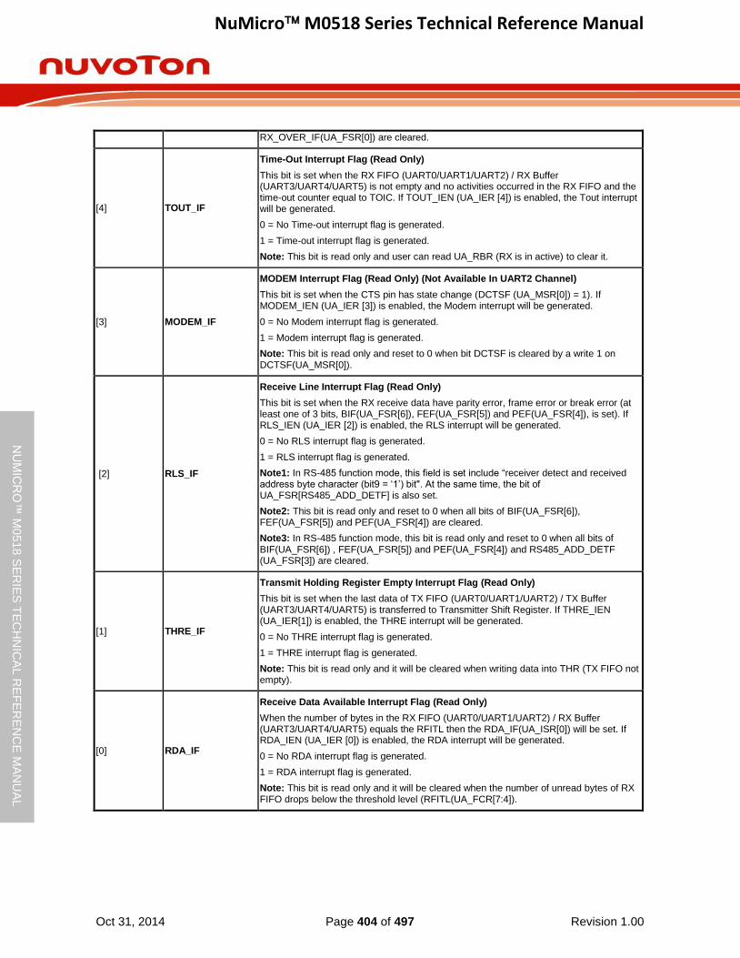
NuMicro M0518 Series Technical Reference Manual
Oct 31, 2014 Page 404 of 497 Revision 1.00
NU
MIC
RO
™ M
0518
SE
RIE
S T
EC
HN
ICA
L R
EF
ER
EN
CE
MA
NU
AL
RX_OVER_IF(UA_FSR[0]) are cleared.
[4] TOUT_IF
Time-Out Interrupt Flag (Read Only)
This bit is set when the RX FIFO (UART0/UART1/UART2) / RX Buffer (UART3/UART4/UART5) is not empty and no activities occurred in the RX FIFO and the time-out counter equal to TOIC. If TOUT_IEN (UA_IER [4]) is enabled, the Tout interrupt will be generated.
0 = No Time-out interrupt flag is generated.
1 = Time-out interrupt flag is generated.
Note: This bit is read only and user can read UA_RBR (RX is in active) to clear it.
[3] MODEM_IF
MODEM Interrupt Flag (Read Only) (Not Available In UART2 Channel)
This bit is set when the CTS pin has state change (DCTSF (UA_MSR[0]) = 1). If MODEM_IEN (UA_IER [3]) is enabled, the Modem interrupt will be generated.
0 = No Modem interrupt flag is generated.
1 = Modem interrupt flag is generated.
Note: This bit is read only and reset to 0 when bit DCTSF is cleared by a write 1 on DCTSF(UA_MSR[0]).
[2] RLS_IF
Receive Line Interrupt Flag (Read Only)
This bit is set when the RX receive data have parity error, frame error or break error (at least one of 3 bits, BIF(UA_FSR[6]), FEF(UA_FSR[5]) and PEF(UA_FSR[4]), is set). If RLS_IEN (UA_IER [2]) is enabled, the RLS interrupt will be generated.
0 = No RLS interrupt flag is generated.
1 = RLS interrupt flag is generated.
Note1: In RS-485 function mode, this field is set include “receiver detect and received address byte character (bit9 = ‘1’) bit". At the same time, the bit of UA_FSR[RS485_ADD_DETF] is also set.
Note2: This bit is read only and reset to 0 when all bits of BIF(UA_FSR[6]), FEF(UA_FSR[5]) and PEF(UA_FSR[4]) are cleared.
Note3: In RS-485 function mode, this bit is read only and reset to 0 when all bits of BIF(UA_FSR[6]) , FEF(UA_FSR[5]) and PEF(UA_FSR[4]) and RS485_ADD_DETF (UA_FSR[3]) are cleared.
[1] THRE_IF
Transmit Holding Register Empty Interrupt Flag (Read Only)
This bit is set when the last data of TX FIFO (UART0/UART1/UART2) / TX Buffer (UART3/UART4/UART5) is transferred to Transmitter Shift Register. If THRE_IEN (UA_IER[1]) is enabled, the THRE interrupt will be generated.
0 = No THRE interrupt flag is generated.
1 = THRE interrupt flag is generated.
Note: This bit is read only and it will be cleared when writing data into THR (TX FIFO not empty).
[0] RDA_IF
Receive Data Available Interrupt Flag (Read Only)
When the number of bytes in the RX FIFO (UART0/UART1/UART2) / RX Buffer (UART3/UART4/UART5) equals the RFITL then the RDA_IF(UA_ISR[0]) will be set. If RDA_IEN (UA_IER [0]) is enabled, the RDA interrupt will be generated.
0 = No RDA interrupt flag is generated.
1 = RDA interrupt flag is generated.
Note: This bit is read only and it will be cleared when the number of unread bytes of RX FIFO drops below the threshold level (RFITL(UA_FCR[7:4]).
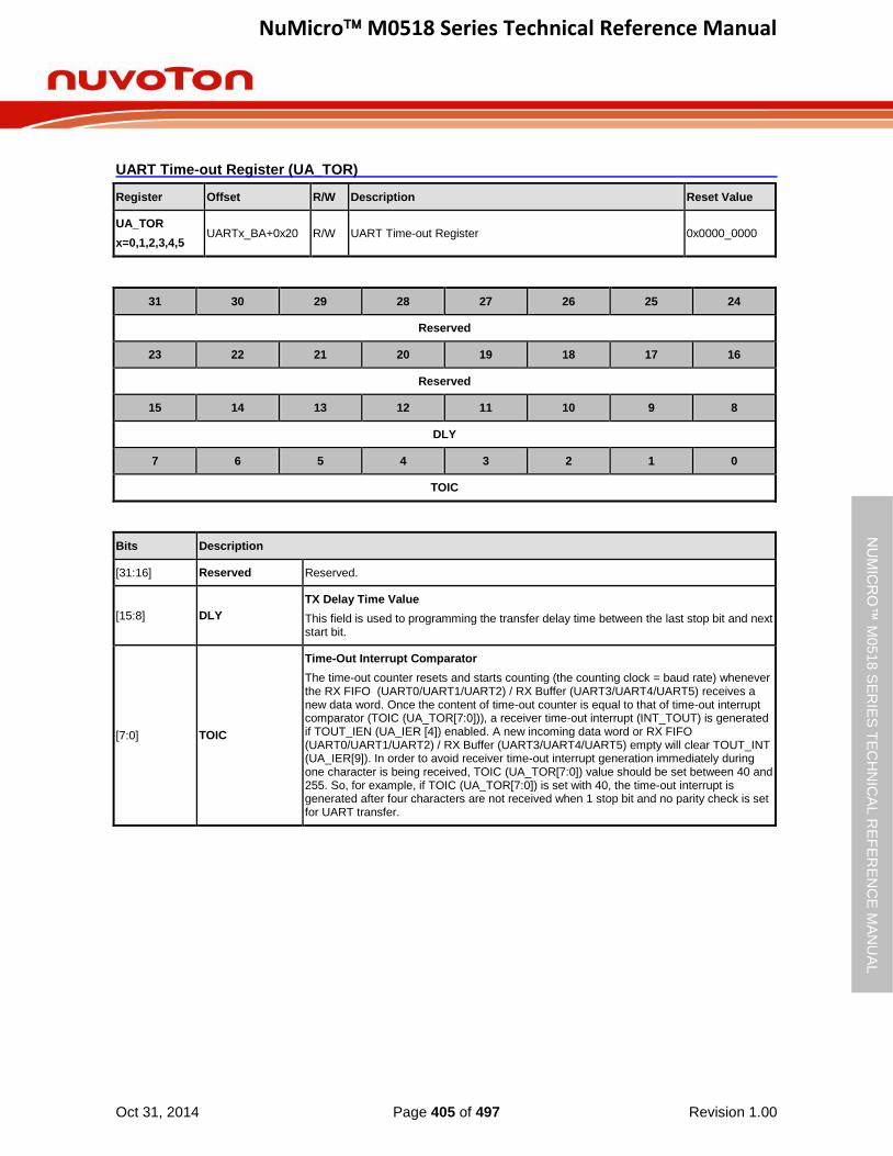
NuMicro M0518 Series Technical Reference Manual
Oct 31, 2014 Page 405 of 497 Revision 1.00
NU
MIC
RO
™ M
0518
SE
RIE
S T
EC
HN
ICA
L R
EF
ER
EN
CE
MA
NU
AL
UART Time-out Register (UA_TOR)
Register Offset R/W Description Reset Value
UA_TOR
x=0,1,2,3,4,5 UARTx_BA+0x20 R/W UART Time-out Register 0x0000_0000
31 30 29 28 27 26 25 24
Reserved
23 22 21 20 19 18 17 16
Reserved
15 14 13 12 11 10 9 8
DLY
7 6 5 4 3 2 1 0
TOIC
Bits Description
[31:16] Reserved Reserved.
[15:8] DLY
TX Delay Time Value
This field is used to programming the transfer delay time between the last stop bit and next start bit.
[7:0] TOIC
Time-Out Interrupt Comparator
The time-out counter resets and starts counting (the counting clock = baud rate) whenever the RX FIFO (UART0/UART1/UART2) / RX Buffer (UART3/UART4/UART5) receives a new data word. Once the content of time-out counter is equal to that of time-out interrupt comparator (TOIC (UA_TOR[7:0])), a receiver time-out interrupt (INT_TOUT) is generated if TOUT_IEN (UA_IER [4]) enabled. A new incoming data word or RX FIFO (UART0/UART1/UART2) / RX Buffer (UART3/UART4/UART5) empty will clear TOUT_INT (UA_IER[9]). In order to avoid receiver time-out interrupt generation immediately during one character is being received, TOIC (UA_TOR[7:0]) value should be set between 40 and 255. So, for example, if TOIC (UA_TOR[7:0]) is set with 40, the time-out interrupt is generated after four characters are not received when 1 stop bit and no parity check is set for UART transfer.
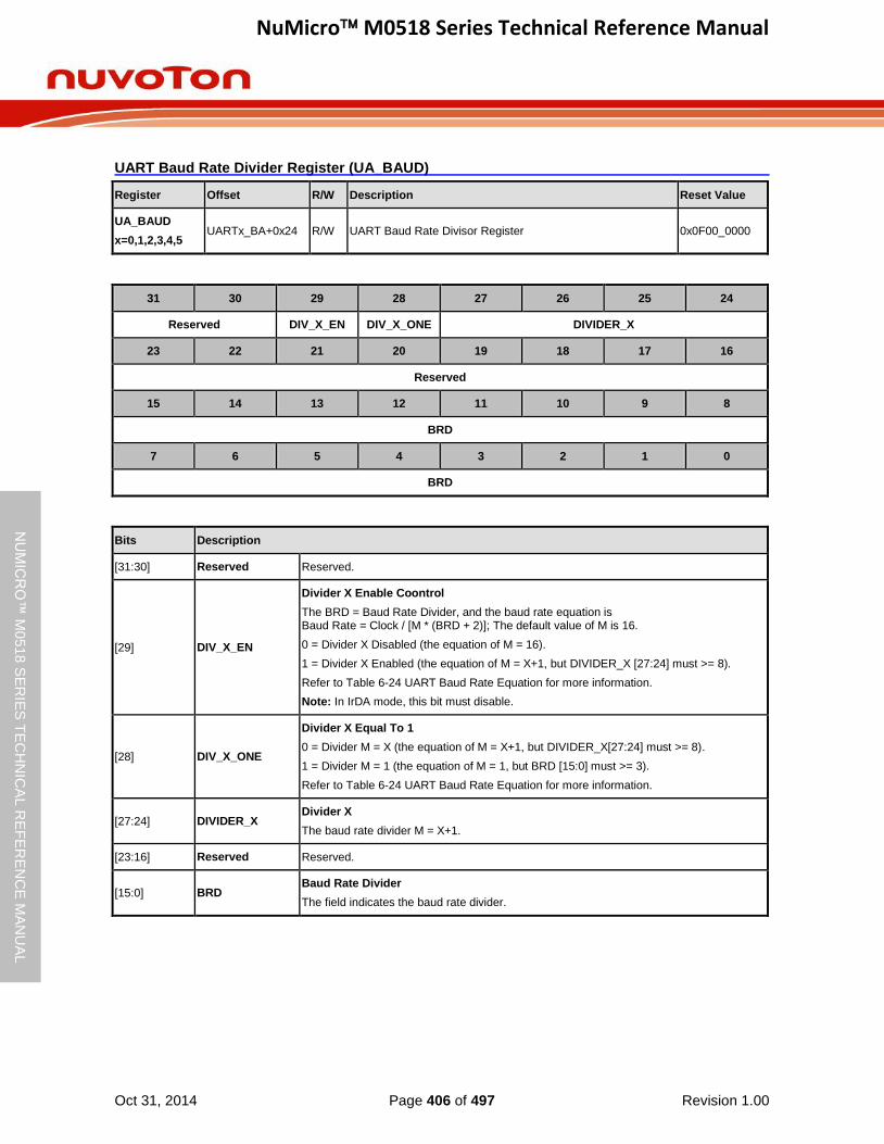
NuMicro M0518 Series Technical Reference Manual
Oct 31, 2014 Page 406 of 497 Revision 1.00
NU
MIC
RO
™ M
0518
SE
RIE
S T
EC
HN
ICA
L R
EF
ER
EN
CE
MA
NU
AL
UART Baud Rate Divider Register (UA_BAUD)
Register Offset R/W Description Reset Value
UA_BAUD
x=0,1,2,3,4,5 UARTx_BA+0x24 R/W UART Baud Rate Divisor Register 0x0F00_0000
31 30 29 28 27 26 25 24
Reserved DIV_X_EN DIV_X_ONE DIVIDER_X
23 22 21 20 19 18 17 16
Reserved
15 14 13 12 11 10 9 8
BRD
7 6 5 4 3 2 1 0
BRD
Bits Description
[31:30] Reserved Reserved.
[29] DIV_X_EN
Divider X Enable Coontrol
The BRD = Baud Rate Divider, and the baud rate equation is Baud Rate = Clock / [M * (BRD + 2)]; The default value of M is 16.
0 = Divider X Disabled (the equation of M = 16).
1 = Divider X Enabled (the equation of M = X+1, but DIVIDER_X [27:24] must >= 8).
Refer to Table 6-24 UART Baud Rate Equation for more information.
Note: In IrDA mode, this bit must disable.
[28] DIV_X_ONE
Divider X Equal To 1
0 = Divider M = X (the equation of M = X+1, but DIVIDER_X[27:24] must >= 8).
1 = Divider M = 1 (the equation of M = 1, but BRD [15:0] must >= 3).
Refer to Table 6-24 UART Baud Rate Equation for more information.
[27:24] DIVIDER_X Divider X
The baud rate divider M = X+1.
[23:16] Reserved Reserved.
[15:0] BRD Baud Rate Divider
The field indicates the baud rate divider.
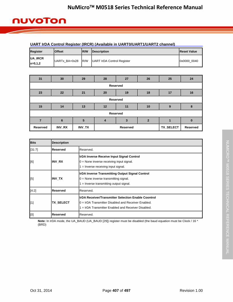
NuMicro M0518 Series Technical Reference Manual
Oct 31, 2014 Page 407 of 497 Revision 1.00
NU
MIC
RO
™ M
0518
SE
RIE
S T
EC
HN
ICA
L R
EF
ER
EN
CE
MA
NU
AL
UART IrDA Control Register (IRCR) (Available in UART0/UART1/UART2 channel)
Register Offset R/W Description Reset Value
UA_IRCR
x=0,1,2 UARTx_BA+0x28 R/W UART IrDA Control Register 0x0000_0040
31 30 29 28 27 26 25 24
Reserved
23 22 21 20 19 18 17 16
Reserved
15 14 13 12 11 10 9 8
Reserved
7 6 5 4 3 2 1 0
Reserved INV_RX INV_TX Reserved TX_SELECT Reserved
Bits Description
[31:7] Reserved Reserved.
[6] INV_RX
IrDA Inverse Receive Input Signal Control
0 = None inverse receiving input signal.
1 = Inverse receiving input signal.
[5] INV_TX
IrDA Inverse Transmitting Output Signal Control
0 = None inverse transmitting signal.
1 = Inverse transmitting output signal.
[4:2] Reserved Reserved.
[1] TX_SELECT
IrDA Receiver/Transmitter Selection Enable Coontrol
0 = IrDA Transmitter Disabled and Receiver Enabled.
1 = IrDA Transmitter Enabled and Receiver Disabled.
[0] Reserved Reserved.
Note: In IrDA mode, the UA_BAUD (UA_BAUD [29]) register must be disabled (the baud equation must be Clock / 16 * (BRD)

NuMicro M0518 Series Technical Reference Manual
Oct 31, 2014 Page 408 of 497 Revision 1.00
NU
MIC
RO
™ M
0518
SE
RIE
S T
EC
HN
ICA
L R
EF
ER
EN
CE
MA
NU
AL
UART Alternate Control/Status Register (UA_ALT_CSR)
Register Offset R/W Description Reset Value
UA_ALT_CSR
x=0,1,2,3,4,5 UARTx_BA+0x2C R/W UART Alternate Control/Status Register 0x0000_000C
31 30 29 28 27 26 25 24
ADDR_MATCH
23 22 21 20 19 18 17 16
Reserved ABRDBITS ABRDEN ABRIF Reserved
15 14 13 12 11 10 9 8
RS485_ADD_EN
Reserved RS485_AUD RS485_AAD RS485_NMM
7 6 5 4 3 2 1 0
LIN_TX_EN LIN_RX_EN Reserved LIN_BKFL
Bits Description
[31:24] ADDR_MATCH
Address Match Value Register (Available In UART0/UART1)
This field contains the RS-485 address match values.
Note: This field is used for RS-485 auto address detection mode.
[23:21] Reserved Reserved.
[20:19] ABRDBITS
Auto-Baud Rate Detect Bit Length
00 = 1-bit time from Start bit to the 1st rising edge. The input pattern shall be 0x01.
01 = 2-bit time from Start bit to the 1st rising edge. The input pattern shall be 0x02.
10 = 4-bit time from Start bit to the 1st rising edge. The input pattern shall be 0x08.
11 = 8-bit time from Start bit to the 1st rising edge. The input pattern shall be 0x80.
Note: The calculation of bit number includes the START bit.
[18] ABRDEN
Auto-Baud Rate Detect Enable Control
0 = Auto-baud rate detect function Disabled.
1 = Auto-baud rate detect function Enabled.
This bit is cleared automatically after auto-baud detection is finished.
[17] ABRIF
Auto-Baud Rate Interrupt Flag (Read Only)
This bit is set when auto-baud rate detection function finished or the auto-baud rate counter was overflow and if ABRIEN(UART_IEN [18]) is set then the auto-baud rate interrupt will be generated.
Note: This bit is read only, but it can be cleared by writing “1” to ABRDTOIF (UA_FSR[2]) and ABRDIF(UA_FSR[1]).
[16] Reserved Reserved.
[15] RS485_ADD_EN
RS-485 Address Detection Enable Coontrol (Available In UART0/UART1)
This bit is used to enable RS-485 Address Detection mode.
0 = Address detection mode Disabled.
1 = Address detection mode Enabled.
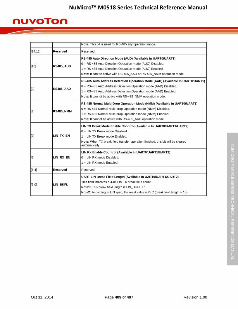
NuMicro M0518 Series Technical Reference Manual
Oct 31, 2014 Page 409 of 497 Revision 1.00
NU
MIC
RO
™ M
0518
SE
RIE
S T
EC
HN
ICA
L R
EF
ER
EN
CE
MA
NU
AL
Note: This bit is used for RS-485 any operation mode.
[14:11] Reserved Reserved.
[10] RS485_AUD
RS-485 Auto Direction Mode (AUD) (Available In UART0/UART1)
0 = RS-485 Auto Direction Operation mode (AUO) Disabled.
1 = RS-485 Auto Direction Operation mode (AUO) Enabled.
Note: It can be active with RS-485_AAD or RS-485_NMM operation mode.
[9] RS485_AAD
RS-485 Auto Address Detection Operation Mode (AAD) (Available In UART0/UART1)
0 = RS-485 Auto Address Detection Operation mode (AAD) Disabled.
1 = RS-485 Auto Address Detection Operation mode (AAD) Enabled.
Note: It cannot be active with RS-485_NMM operation mode.
[8] RS485_NMM
RS-485 Normal Multi-Drop Operation Mode (NMM) (Available In UART0/UART1)
0 = RS-485 Normal Multi-drop Operation mode (NMM) Disabled.
1 = RS-485 Normal Multi-drop Operation mode (NMM) Enabled.
Note: It cannot be active with RS-485_AAD operation mode.
[7] LIN_TX_EN
LIN TX Break Mode Enable Coontrol (Available In UART0/UART1/UART2)
0 = LIN TX Break mode Disabled.
1 = LIN TX Break mode Enabled.
Note: When TX break field transfer operation finished, this bit will be cleared automatically.
[6] LIN_RX_EN
LIN RX Enable Coontrol (Available In UART0/UART1/UART2)
0 = LIN RX mode Disabled.
1 = LIN RX mode Enabled.
[5:4] Reserved Reserved.
[3:0] LIN_BKFL
UART LIN Break Field Length (Available In UART0/UART1/UART2)
This field indicates a 4-bit LIN TX break field count.
Note1: This break field length is LIN_BKFL + 1.
Note2: According to LIN spec, the reset value is 0xC (break field length = 13).
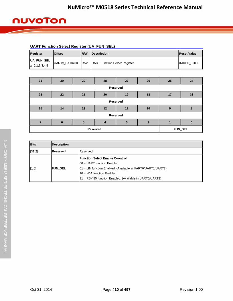
NuMicro M0518 Series Technical Reference Manual
Oct 31, 2014 Page 410 of 497 Revision 1.00
NU
MIC
RO
™ M
0518
SE
RIE
S T
EC
HN
ICA
L R
EF
ER
EN
CE
MA
NU
AL
UART Function Select Register (UA_FUN_SEL)
Register Offset R/W Description Reset Value
UA_FUN_SEL
x=0,1,2,3,4,5 UARTx_BA+0x30 R/W UART Function Select Register 0x0000_0000
31 30 29 28 27 26 25 24
Reserved
23 22 21 20 19 18 17 16
Reserved
15 14 13 12 11 10 9 8
Reserved
7 6 5 4 3 2 1 0
Reserved FUN_SEL
Bits Description
[31:2] Reserved Reserved.
[1:0] FUN_SEL
Function Select Enable Coontrol
00 = UART function Enabled.
01 = LIN function Enabled. (Available in UART0/UART1/UART2)
10 = IrDA function Enabled.
11 = RS-485 function Enabled. (Available in UART0/UART1)
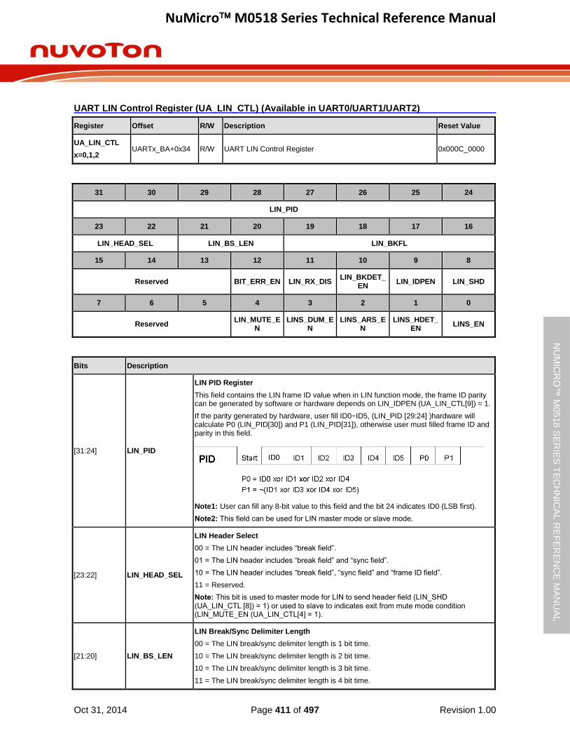
NuMicro M0518 Series Technical Reference Manual
Oct 31, 2014 Page 411 of 497 Revision 1.00
NU
MIC
RO
™ M
0518
SE
RIE
S T
EC
HN
ICA
L R
EF
ER
EN
CE
MA
NU
AL
UART LIN Control Register (UA_LIN_CTL) (Available in UART0/UART1/UART2)
Register Offset R/W Description Reset Value
UA_LIN_CTL
x=0,1,2 UARTx_BA+0x34 R/W UART LIN Control Register 0x000C_0000
31 30 29 28 27 26 25 24
LIN_PID
23 22 21 20 19 18 17 16
LIN_HEAD_SEL LIN_BS_LEN LIN_BKFL
15 14 13 12 11 10 9 8
Reserved BIT_ERR_EN LIN_RX_DIS LIN_BKDET_
EN LIN_IDPEN LIN_SHD
7 6 5 4 3 2 1 0
Reserved LIN_MUTE_E
N LINS_DUM_E
N LINS_ARS_E
N LINS_HDET_
EN LINS_EN
Bits Description
[31:24] LIN_PID
LIN PID Register
This field contains the LIN frame ID value when in LIN function mode, the frame ID parity can be generated by software or hardware depends on LIN_IDPEN (UA_LIN_CTL[9]) = 1.
If the parity generated by hardware, user fill ID0~ID5, (LIN_PID [29:24] )hardware will calculate P0 (LIN_PID[30]) and P1 (LIN_PID[31]), otherwise user must filled frame ID and parity in this field.
Note1: User can fill any 8-bit value to this field and the bit 24 indicates ID0 (LSB first).
Note2: This field can be used for LIN master mode or slave mode.
[23:22] LIN_HEAD_SEL
LIN Header Select
00 = The LIN header includes “break field”.
01 = The LIN header includes “break field” and “sync field”.
10 = The LIN header includes “break field”, “sync field” and “frame ID field”.
11 = Reserved.
Note: This bit is used to master mode for LIN to send header field (LIN_SHD (UA_LIN_CTL [8]) = 1) or used to slave to indicates exit from mute mode condition (LIN_MUTE_EN (UA_LIN_CTL[4] = 1).
[21:20] LIN_BS_LEN
LIN Break/Sync Delimiter Length
00 = The LIN break/sync delimiter length is 1 bit time.
10 = The LIN break/sync delimiter length is 2 bit time.
10 = The LIN break/sync delimiter length is 3 bit time.
11 = The LIN break/sync delimiter length is 4 bit time.

NuMicro M0518 Series Technical Reference Manual
Oct 31, 2014 Page 412 of 497 Revision 1.00
NU
MIC
RO
™ M
0518
SE
RIE
S T
EC
HN
ICA
L R
EF
ER
EN
CE
MA
NU
AL
Protected Identifier field
Header
Synch fieldBreak Field
Inter-byte spacesBreak/Sync
Delimiter Length
Note: This bit used for LIN master to sending header field.
[19:16] LIN_BKFL
LIN Break Field Length
This field indicates a 4-bit LIN TX break field count.
Note1: These registers are shadow registers of LIN_BKFL, User can read/write it by setting LIN_BKFL (UA_ALT_CSR[3:0]) or LIN_BKFL (UA_LIN_CTL[19:16].
Note2: This break field length is LIN_BKFL + 1.
Note3: According to LIN spec, the reset value is 12 (break field length = 13).
[15:13] Reserved Reserved.
[12] BIT_ERR_EN
Bit Error Detect Enable Coontrol
0 = Bit error detection function Disabled.
1 = Bit error detection Enabled.
Note: In LIN function mode, when occur bit error, the BIT_ERR_F (UA_LIN_SR[9]) flag will be asserted. If the LIN_IEN (UA_IER[8]) = 1, an interrupt will be generated.
[11] LIN_RX_DIS
LIN Receiver Disable Bit
If the receiver is enabled (LIN_RX_DIS (UA_LIN_CTL[11] ) = 0), all received byte data will be accepted and stored in the RX-FIFO, and if the receiver is disabled (LIN_RX_DIS (UA_LIN_CTL[11] = 1), all received byte data will be ignore.
0 = LIN receiver Enabled.
1 = LIN receiver Disabled.
Note: This bit is only valid when operating in LIN function mode (FUN_SEL (UA_FUN_SEL[1:0]) = 01).
[10] LIN_BKDET_EN
LIN Break Detection Enable Coontrol
When detect consecutive dominant greater than 11 bits, and are followed by a delimiter character, the LIN_BKDET_F (UA_LIN_SR[8]) flag is set in UA_LIN_SR register at the end of break field. If the LIN_IEN (UA_IER [8])=1, an interrupt will be generated.
0 = LIN break detection Disabled.
1 = LIN break detection Enabled.
[9] LIN_IDPEN
LIN ID Parity Enable Coontrol
0 = LIN frame ID parity Disabled.
1 = LIN frame ID parity Enabled.
Note1: This bit can be used for LIN master to sending header field (LIN_SHD (UA_LIN_CTL[8])) = 1 and LIN_HEAD_SEL (UA_LIN_CTL[23:22]) = 10) or be used for enable LIN slave received frame ID parity checked.
Note2: This bit is only use when the operation header transmitter is in LIN_HEAD_SEL (UA_LIN_CTL[23:22]) = 10.
[8] LIN_SHD
LIN TX Send Header Enable Coontrol
The LIN TX header can be “break field” or “break and sync field” or “break, sync and frame ID field”, it is depend on setting LIN_HEAD_SEL (UA_LIN_CTL[23:22]).
0 = Send LIN TX header Disabled.
1 = Send LIN TX header Enabled.
Note1: These registers are shadow registers of LIN_SHD (UA_ALT_CSR [7]); user can
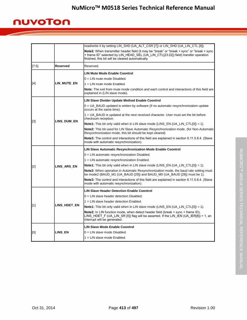
NuMicro M0518 Series Technical Reference Manual
Oct 31, 2014 Page 413 of 497 Revision 1.00
NU
MIC
RO
™ M
0518
SE
RIE
S T
EC
HN
ICA
L R
EF
ER
EN
CE
MA
NU
AL
read/write it by setting LIN_SHD (UA_ALT_CSR [7]) or LIN_SHD (UA_LIN_CTL [8]).
Note2: When transmitter header field (it may be “break” or “break + sync” or “break + sync + frame ID” selected by LIN_HEAD_SEL (UA_LIN_CTL[23:22]) field) transfer operation finished, this bit will be cleared automatically.
[7:5] Reserved Reserved.
[4] LIN_MUTE_EN
LIN Mute Mode Enable Coontrol
0 = LIN mute mode Disabled.
1 = LIN mute mode Enabled.
Note: The exit from mute mode condition and each control and interactions of this field are explained in (LIN slave mode).
[3] LINS_DUM_EN
LIN Slave Divider Update Method Enable Coontrol
0 = UA_BAUD updated is written by software (if no automatic resynchronization update occurs at the same time).
1 = UA_BAUD is updated at the next received character. User must set the bit before checksum reception.
Note1: This bit only valid when in LIN slave mode (LINS_EN (UA_LIN_CTL[0]) = 1).
Note2: This bit used for LIN Slave Automatic Resynchronization mode. (for Non-Automatic Resynchronization mode, this bit should be kept cleared)
Note3: The control and interactions of this field are explained in section 6.11.5.8.4. (Slave mode with automatic resynchronization).
[2] LINS_ARS_EN
LIN Slave Automatic Resynchronization Mode Enable Coontrol
0 = LIN automatic resynchronization Disabled.
1 = LIN automatic resynchronization Enabled.
Note1: This bit only valid when in LIN slave mode (LINS_EN (UA_LIN_CTL[0]) = 1).
Note2: When operation in Automatic Resynchronization mode, the baud rate setting must be mode2 (BAUD_M1 (UA_BAUD [29]) and BAUD_M0 (UA_BAUD [28]) must be 1).
Note3: The control and interactions of this field are explained in section 6.11.5.8.4. (Slave mode with automatic resynchronization).
[1] LINS_HDET_EN
LIN Slave Header Detection Enable Coontrol
0 = LIN slave header detection Disabled.
1 = LIN slave header detection Enabled.
Note1: This bit only valid when in LIN slave mode (LINS_EN (UA_LIN_CTL[0]) = 1).
Note2: In LIN function mode, when detect header field (break + sync + frame ID), LINS_HDET_F (UA_LIN_SR [0]) flag will be asserted. If the LIN_IEN (UA_IER[8]) = 1, an interrupt will be generated.
[0] LINS_EN
LIN Slave Mode Enable Coontrol
0 = LIN slave mode Disabled.
1 = LIN slave mode Enabled.
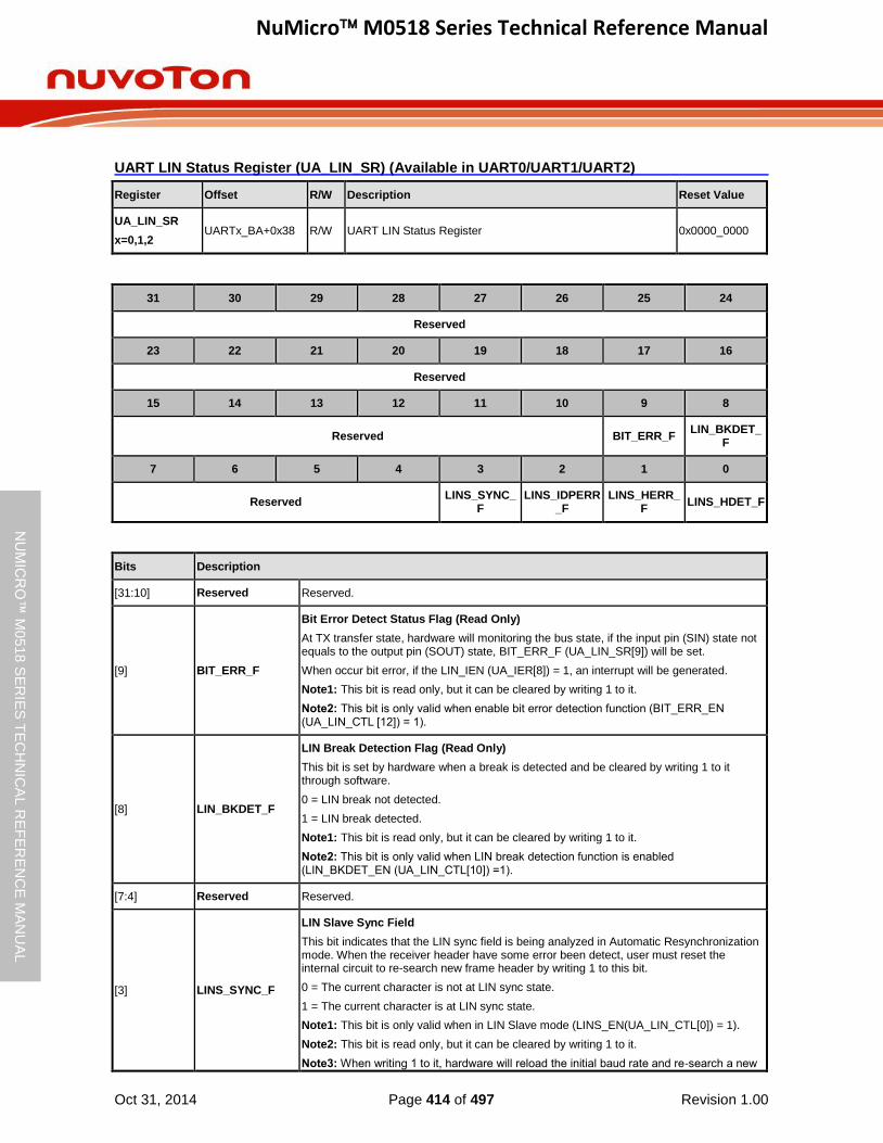
NuMicro M0518 Series Technical Reference Manual
Oct 31, 2014 Page 414 of 497 Revision 1.00
NU
MIC
RO
™ M
0518
SE
RIE
S T
EC
HN
ICA
L R
EF
ER
EN
CE
MA
NU
AL
UART LIN Status Register (UA_LIN_SR) (Available in UART0/UART1/UART2)
Register Offset R/W Description Reset Value
UA_LIN_SR
x=0,1,2 UARTx_BA+0x38 R/W UART LIN Status Register 0x0000_0000
31 30 29 28 27 26 25 24
Reserved
23 22 21 20 19 18 17 16
Reserved
15 14 13 12 11 10 9 8
Reserved BIT_ERR_F LIN_BKDET_
F
7 6 5 4 3 2 1 0
Reserved LINS_SYNC_
F LINS_IDPERR
_F LINS_HERR_
F LINS_HDET_F
Bits Description
[31:10] Reserved Reserved.
[9] BIT_ERR_F
Bit Error Detect Status Flag (Read Only)
At TX transfer state, hardware will monitoring the bus state, if the input pin (SIN) state not equals to the output pin (SOUT) state, BIT_ERR_F (UA_LIN_SR[9]) will be set.
When occur bit error, if the LIN_IEN (UA_IER[8]) = 1, an interrupt will be generated.
Note1: This bit is read only, but it can be cleared by writing 1 to it.
Note2: This bit is only valid when enable bit error detection function (BIT_ERR_EN (UA_LIN_CTL [12]) = 1).
[8] LIN_BKDET_F
LIN Break Detection Flag (Read Only)
This bit is set by hardware when a break is detected and be cleared by writing 1 to it through software.
0 = LIN break not detected.
1 = LIN break detected.
Note1: This bit is read only, but it can be cleared by writing 1 to it.
Note2: This bit is only valid when LIN break detection function is enabled (LIN_BKDET_EN (UA_LIN_CTL[10]) =1).
[7:4] Reserved Reserved.
[3] LINS_SYNC_F
LIN Slave Sync Field
This bit indicates that the LIN sync field is being analyzed in Automatic Resynchronization mode. When the receiver header have some error been detect, user must reset the internal circuit to re-search new frame header by writing 1 to this bit.
0 = The current character is not at LIN sync state.
1 = The current character is at LIN sync state.
Note1: This bit is only valid when in LIN Slave mode (LINS_EN(UA_LIN_CTL[0]) = 1).
Note2: This bit is read only, but it can be cleared by writing 1 to it.
Note3: When writing 1 to it, hardware will reload the initial baud rate and re-search a new
NuMicro M0518 Series Technical Reference Manual
Oct 31, 2014 Page 415 of 497 Revision 1.00
NU
MIC
RO
™ M
0518
SE
RIE
S T
EC
HN
ICA
L R
EF
ER
EN
CE
MA
NU
AL
frame header.
[2] LINS_IDPERR_F
LIN Slave ID Parity Error Flag (Read Only)
This bit is set by hardware when receipted frame ID parity is not correct.
0 = No active.
1 = Receipted frame ID parity is not correct.
Note1: This bit is read only, but it can be cleared by writing “1” to it.
Note2: This bit is only valid when in LIN slave mode (LINS_EN (UA_LIN_CTL [0])= 1) and enable LIN frame ID parity check function LIN_IDPEN (UA_LIN_CTL [9]).
[1] LINS_HERR_F
LIN Slave Header Error Flag (Read Only)
This bit is set by hardware when a LIN header error is detected in LIN slave mode and be cleared by writing 1 to it. The header errors include “break delimiter is too short (less than 0.5 bit time)”, “frame error in sync field or Identifier field”, “sync field data is not 0x55 in Non-Automatic Resynchronization mode”, “sync field deviation error with Automatic Resynchronization mode”, “sync field measure time-out with Automatic Resynchronization mode” and “LIN header reception time-out”.
0 = LIN header error not detected.
1 = LIN header error detected.
Note1: This bit is read only, but it can be cleared by writing 1 to it.
Note2: This bit is only valid when UART is operated in LIN slave mode (LINS_EN (UA_LIN_CTL [0]) = 1) and enables LIN slave header detection function (LINS_HDET_EN (UA_LIN_CTL [1])).
[0] LINS_HDET_F
LIN Slave Header Detection Flag (Read Only)
This bit is set by hardware when a LIN header is detected in LIN slave mode and be cleared by writing 1 to it.
0 = LIN header not detected.
1 = LIN header detected (break + sync + frame ID).
Note1: This bit is read only, but it can be cleared by writing 1 to it.
Note2: This bit is only valid when in LIN slave mode (LINS_EN (UA_LIN_CTL [0]) = 1) and enable LIN slave header detection function (LINS_HDET_EN (UA_LIN_CTL [1])).
Note3: When enable ID parity check LIN_IDPEN (UA_LIN_CTL [9]), if hardware detect complete header (“break + sync + frame ID”), the LINS_HEDT_F will be set whether the frame ID correct or not.
NuMicro M0518 Series Technical Reference Manual
Oct 31, 2014 Page 416 of 497 Revision 1.00
NU
MIC
RO
™ M
0518
SE
RIE
S T
EC
HN
ICA
L R
EF
ER
EN
CE
MA
NU
AL
6.12 I2C Serial Interface Controller (I2C)
6.12.1 Overview
I2C is a two-wire, bi-directional serial bus that provides a simple and efficient method of data exchange
between devices. The I2C standard is a true multi-master bus including collision detection and
arbitration that prevents data corruption if two or more masters attempt to control the bus simultaneously.
6.12.2 Features
The I2C bus uses two wires (I2Cn_SDA and I2Cn_SCL) to transfer information between devices
connected to the bus. The main features of the I2C bus include:
Supports up to two I2C serial interface controller
Master/Slave mode
Bidirectional data transfer between masters and slaves
Multi-master bus (no central master)
Arbitration between simultaneously transmitting masters without corruption of serial data on the bus
Serial clock synchronization allow devices with different bit rates to communicate via one serial bus
Built-in a 14-bit time-out counter requesting the I2C interrupt if the I
2C bus hangs up and
timer-out counter overflows.
Programmable clocks allow for versatile rate control
Supports 7-bit addressing mode
Supports multiple address recognition ( four slave address with mask option)
Supports Power-down wake-up function
6.12.3 Basic Configuration
The basic configurations of I2C0 are as follows:
I2C0 pins are configured on GPA_MFP [9:8] register
Enable I2C0 clock by setting I2C0_EN (APBCLK [8])
Reset I2C0 controller by setting I2C0_RST(IPRSTC2 [8])
The basic configurations of I2C1 are as follows:
I2C1 pins are configured on GPE_MFP [11:10] register
Enable I2C1 clock by setting I2C1_EN( APBCLK [9])

NuMicro M0518 Series Technical Reference Manual
Oct 31, 2014 Page 417 of 497 Revision 1.00
NU
MIC
RO
™ M
0518
SE
RIE
S T
EC
HN
ICA
L R
EF
ER
EN
CE
MA
NU
AL
Reset I2C1 controller by setting I2C1_RST (IPRSTC2 [9])
6.12.4 Block Diagram
The basic configurations of I2C are as follows:
Control Register
APB Interface
Bus Clock Control
Wakeup Control
Bus Protocol Interface Control
I2Cn_SCL
I2Cn_SDA
Figure 6-106 I2C Controller Block Diagram
6.12.5 Functional Description
On I2C bus, data is transferred between a Master and a Slave. Data bits transfer on the
I2Cn_SCL and I2Cn_SDA lines are synchronously on a byte-by-byte basis. Each data byte is 8-bit long. There is one I2Cn_SCL clock pulse for each data bit with the MSB being transmitted first, and an acknowledge bit follows each transferred byte. Each bit is sampled during the high period of I2Cn_SCL; therefore, the I2Cn_SDA line may be changed only during the low period of I2Cn_SCL and must be held stable during the high period of I2Cn_SCL. A transition on the I2Cn_SDA line while I2Cn_SCL is high is interpreted as a command (START or STOP). Please refer to the following figure for more detailed I
2C bus timing.
tBUF
STOP
I2Cn_SDA
I2Cn_SCL
START
tHD;STA
tLOW
tHD;DAT
tHIGH
tf
tSU;DAT
Repeated
START
tSU;STA tSU;STO
STOP
tr
Figure 6-107 I2C Bus Timing
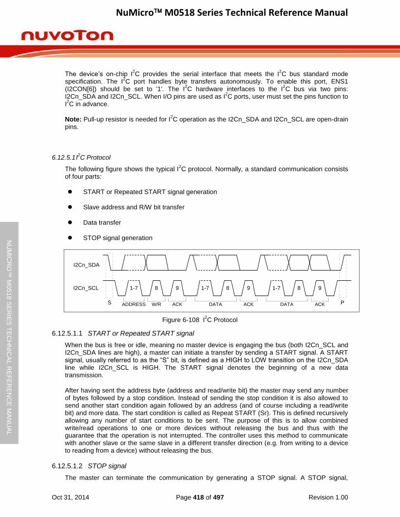
NuMicro M0518 Series Technical Reference Manual
Oct 31, 2014 Page 418 of 497 Revision 1.00
NU
MIC
RO
™ M
0518
SE
RIE
S T
EC
HN
ICA
L R
EF
ER
EN
CE
MA
NU
AL
The device’s on-chip I2C provides the serial interface that meets the I
2C bus standard mode
specification. The I2C port handles byte transfers autonomously. To enable this port, ENS1
(I2CON[6]) should be set to '1'. The I2C hardware interfaces to the I
2C bus via two pins:
I2Cn_SDA and I2Cn_SCL. When I/O pins are used as I2C ports, user must set the pins function to
I2C in advance.
Note: Pull-up resistor is needed for I2C operation as the I2Cn_SDA and I2Cn_SCL are open-drain
pins.
6.12.5.1 I2C Protocol
The following figure shows the typical I2C protocol. Normally, a standard communication consists
of four parts:
START or Repeated START signal generation
Slave address and R/W bit transfer
Data transfer
STOP signal generation
I2Cn_SDA
I2Cn_SCL 1-7 8 9
S
1-7 8 9 1-7 8 9
PADDRESS W/R ACK DATA ACK DATA ACK
Figure 6-108 I2C Protocol
6.12.5.1.1 START or Repeated START signal
When the bus is free or idle, meaning no master device is engaging the bus (both I2Cn_SCL and I2Cn_SDA lines are high), a master can initiate a transfer by sending a START signal. A START signal, usually referred to as the “S” bit, is defined as a HIGH to LOW transition on the I2Cn_SDA line while I2Cn_SCL is HIGH. The START signal denotes the beginning of a new data transmission.
After having sent the address byte (address and read/write bit) the master may send any number of bytes followed by a stop condition. Instead of sending the stop condition it is also allowed to send another start condition again followed by an address (and of course including a read/write bit) and more data. The start condition is called as Repeat START (Sr). This is defined recursively allowing any number of start conditions to be sent. The purpose of this is to allow combined write/read operations to one or more devices without releasing the bus and thus with the guarantee that the operation is not interrupted. The controller uses this method to communicate with another slave or the same slave in a different transfer direction (e.g. from writing to a device to reading from a device) without releasing the bus.
6.12.5.1.2 STOP signal
The master can terminate the communication by generating a STOP signal. A STOP signal,

NuMicro M0518 Series Technical Reference Manual
Oct 31, 2014 Page 419 of 497 Revision 1.00
NU
MIC
RO
™ M
0518
SE
RIE
S T
EC
HN
ICA
L R
EF
ER
EN
CE
MA
NU
AL
usually referred to as the “P” bit, is defined as a LOW to HIGH transition on the I2Cn_SDA line while I2Cn_SCL is HIGH.
The following figure shows the waveform of START, Repeat START and STOP.
STOP
I2Cn_SDA
I2Cn_SCL
START START STOP
Figure 6-109 START and STOP Conditions
6.12.5.1.3 Slave Address Transfer
The first byte of data transferred by the master immediately after the START signal is the Slave address (SLA). This is a 7-bit calling address followed by a Read/Write (R/W) bit. The R/W bit signals of the slave indicate the data transfer direction. No two slaves in the system can have the same address. Only the slave with an address that matches the one transmitted by the master will respond by returning an acknowledge bit by pulling the I2Cn_SDA low at the 9th I2Cn_SCL clock cycle.
6.12.5.1.4 Data Transfer
When a slave receives a correct address with an R/W bit, the data will follow R/W bit specified to transfer. Each transferred byte is followed by an acknowledge bit on the 9th I2Cn_SCL clock cycle. If the slave signals a Not Acknowledge (NACK), the master can generate a STOP signal to abort the data transfer or generate a Repeated START signal and start a new transfer cycle.
If the master, as a receiving device, does Not Acknowledge (NACK) the slave, the slave releases the I2Cn_SDA line for the master to generate a STOP or Repeated START signal.
I2Cn_SDA
I2Cn_SCL
Data line stable;
data valid
Change of data
allowed
Figure 6-110 Bit Transfer on the I2C Bus
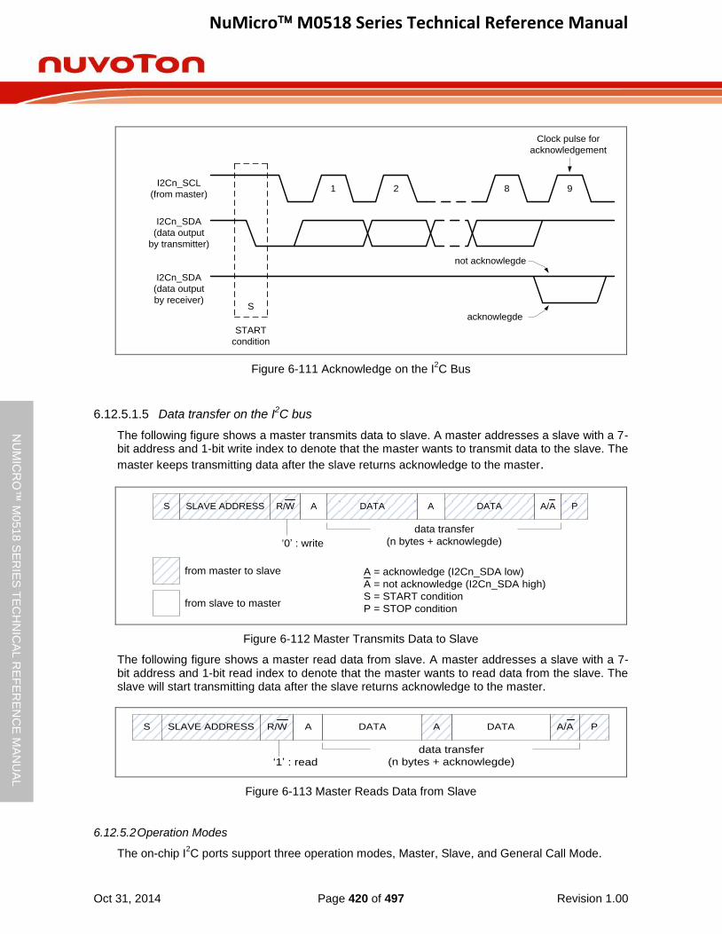
NuMicro M0518 Series Technical Reference Manual
Oct 31, 2014 Page 420 of 497 Revision 1.00
NU
MIC
RO
™ M
0518
SE
RIE
S T
EC
HN
ICA
L R
EF
ER
EN
CE
MA
NU
AL
I2Cn_SDA
(data output
by transmitter)
I2Cn_SCL
(from master)
START
condition
acknowlegde
I2Cn_SDA
(data output
by receiver)S
1 2 8 9
Clock pulse for
acknowledgement
not acknowlegde
Figure 6-111 Acknowledge on the I2C Bus
6.12.5.1.5 Data transfer on the I2C bus
The following figure shows a master transmits data to slave. A master addresses a slave with a 7-bit address and 1-bit write index to denote that the master wants to transmit data to the slave. The
master keeps transmitting data after the slave returns acknowledge to the master.
A = acknowledge (I2Cn_SDA low)
A = not acknowledge (I2Cn_SDA high)
S = START condition
P = STOP condition
‘0’ : write
S SLAVE ADDRESS R/W A DATA A DATA A/A P
from master to slave
from slave to master
data transfer
(n bytes + acknowlegde)
Figure 6-112 Master Transmits Data to Slave
The following figure shows a master read data from slave. A master addresses a slave with a 7-bit address and 1-bit read index to denote that the master wants to read data from the slave. The slave will start transmitting data after the slave returns acknowledge to the master.
‘1’ : read
S SLAVE ADDRESS R/W A DATA A DATA A/A P
data transfer
(n bytes + acknowlegde)
Figure 6-113 Master Reads Data from Slave
6.12.5.2 Operation Modes
The on-chip I2C ports support three operation modes, Master, Slave, and General Call Mode.
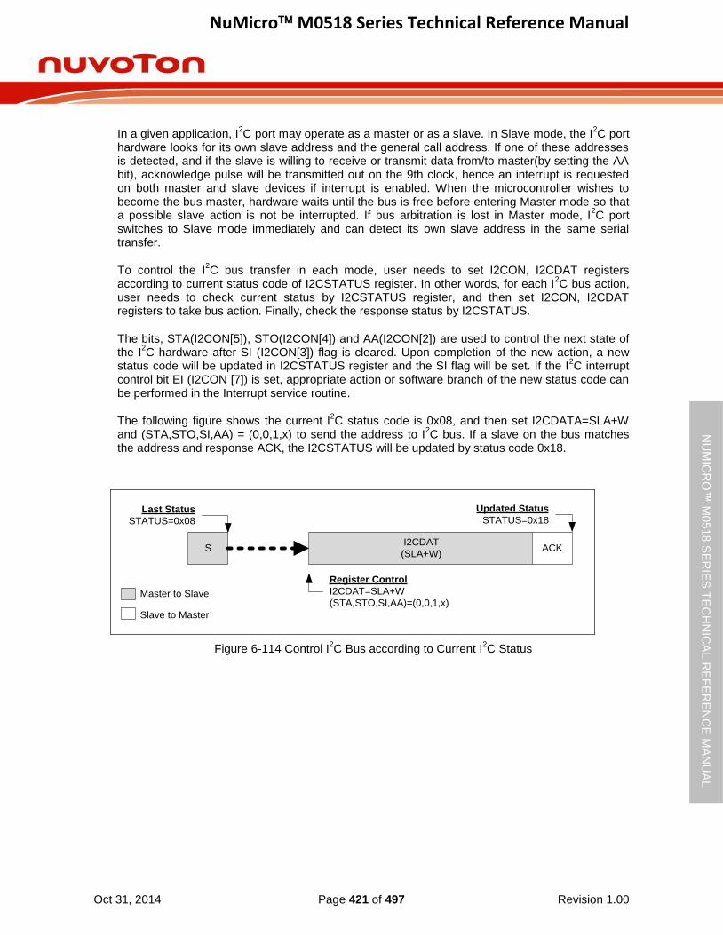
NuMicro M0518 Series Technical Reference Manual
Oct 31, 2014 Page 421 of 497 Revision 1.00
NU
MIC
RO
™ M
0518
SE
RIE
S T
EC
HN
ICA
L R
EF
ER
EN
CE
MA
NU
AL
In a given application, I2C port may operate as a master or as a slave. In Slave mode, the I
2C port
hardware looks for its own slave address and the general call address. If one of these addresses is detected, and if the slave is willing to receive or transmit data from/to master(by setting the AA bit), acknowledge pulse will be transmitted out on the 9th clock, hence an interrupt is requested on both master and slave devices if interrupt is enabled. When the microcontroller wishes to become the bus master, hardware waits until the bus is free before entering Master mode so that a possible slave action is not be interrupted. If bus arbitration is lost in Master mode, I
2C port
switches to Slave mode immediately and can detect its own slave address in the same serial transfer.
To control the I2C bus transfer in each mode, user needs to set I2CON, I2CDAT registers
according to current status code of I2CSTATUS register. In other words, for each I2C bus action,
user needs to check current status by I2CSTATUS register, and then set I2CON, I2CDAT registers to take bus action. Finally, check the response status by I2CSTATUS.
The bits, STA(I2CON[5]), STO(I2CON[4]) and AA(I2CON[2]) are used to control the next state of the I
2C hardware after SI (I2CON[3]) flag is cleared. Upon completion of the new action, a new
status code will be updated in I2CSTATUS register and the SI flag will be set. If the I2C interrupt
control bit EI (I2CON [7]) is set, appropriate action or software branch of the new status code can be performed in the Interrupt service routine.
The following figure shows the current I2C status code is 0x08, and then set I2CDATA=SLA+W
and (STA,STO,SI,AA) = (0,0,1,x) to send the address to I2C bus. If a slave on the bus matches
the address and response ACK, the I2CSTATUS will be updated by status code 0x18.
SI2CDAT
(SLA+W)ACK
Last Status
STATUS=0x08
Updated Status
STATUS=0x18
Register Control
I2CDAT=SLA+W
(STA,STO,SI,AA)=(0,0,1,x)Master to Slave
Slave to Master
Figure 6-114 Control I2C Bus according to Current I
2C Status
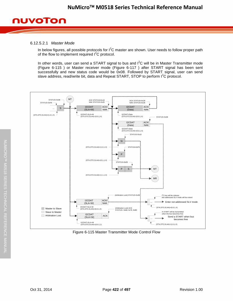
NuMicro M0518 Series Technical Reference Manual
Oct 31, 2014 Page 422 of 497 Revision 1.00
NU
MIC
RO
™ M
0518
SE
RIE
S T
EC
HN
ICA
L R
EF
ER
EN
CE
MA
NU
AL
6.12.5.2.1 Master Mode
In below figures, all possible protocols for I2C master are shown. User needs to follow proper path
of the flow to implement required I2C protocol.
In other words, user can send a START signal to bus and I2C will be in Master Transmitter mode
(Figure 6-115 ) or Master receiver mode (Figure 6-117 ) after START signal has been sent successfully and new status code would be 0x08. Followed by START signal, user can send slave address, read/write bit, data and Repeat START, STOP to perform I
2C protocol.
SI2CDAT
(SLA+W)
ACK/
NAK
Master to Slave
Slave to Master
I2CDAT
(Data)
ACK/
NAK
Sr
P
P S
STATUS=0x08
(STA,STO,SI,AA)=(1,0,1,X)
ACK STATUS=0x18
NAK STATUS=0x20
I2CDAT=SLA+W
(STA,STO,SI,AA)=(0,0,1,X)
ACK STATUS=0x28
NAK STATUS=0x30
I2CDAT=Data
(STA,STO,SI,AA)=(0,0,1,X)
STATUS=0x10
(STA,STO,SI,AA)=(1,0,1,X) STATUS=0xF8
(STA,STO,SI,AA)=(0,1,1,X)STATUS=0x08
(STA,STO,SI,AA)=(1,1,1,X)
I2CDAT
(SLA+W)
ACK/
NAK
(Arbitration Lost) STATUS=0x38
I2CDAT=SLA+W
(STA,STO,SI,AA)=(0,0,1,X)
I2CDAT
(Data)
ACK/
NAK
STATUS=0x38
I2CDAT=Data
(STA,STO,SI,AA)=(0,0,1,X)
Arbitration LostI2CDAT
(SLA+W)
I2CDAT=SLA+W
(STA,STO,SI,AA)=(0,0,1,1)
(Arbitration Lost) ACK
STATUS= 0x68, 0x78, 0xB0
ACK
(STA,STO,SI,AA)=(0,0,1,X)
...
I2C bus will be release;
Not addressed SLV mode will be enterd
...
(STA,STO,SI,AA)=(1,0,1,X)
A START will be transmitted
when the bus becomes free
Enter not addressed SLV mode
Send a START when bus
becomes free
MT
MT
MR
...
STATUS=0xF8
Figure 6-115 Master Transmitter Mode Control Flow
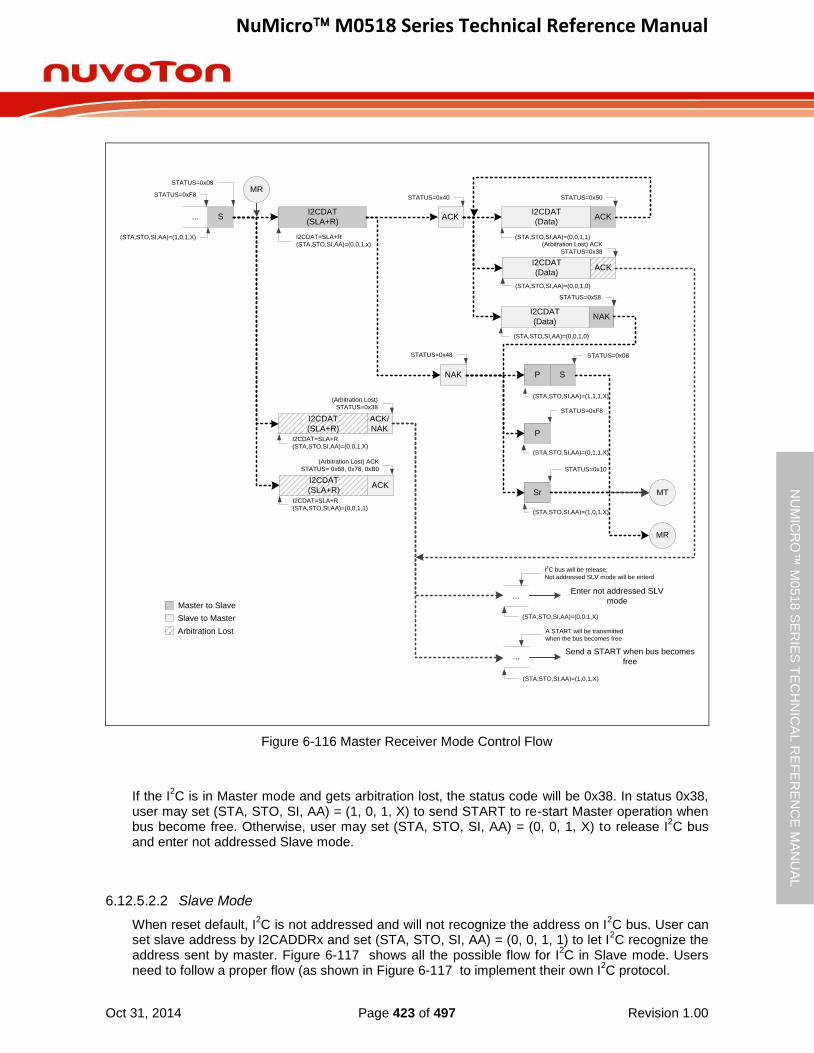
NuMicro M0518 Series Technical Reference Manual
Oct 31, 2014 Page 423 of 497 Revision 1.00
NU
MIC
RO
™ M
0518
SE
RIE
S T
EC
HN
ICA
L R
EF
ER
EN
CE
MA
NU
AL
I2CDAT
(SLA+R)ACK
NAK
I2CDAT
(Data)NAK
I2CDAT
(Data)ACK
P S
P
Sr
I2CDAT=SLA+R
(STA,STO,SI,AA)=(0,0,1,x)
STATUS=0x40
STATUS=0x48 STATUS=0x08
STATUS=0xF8
STATUS=0x10
STATUS=0x50
STATUS=0x58
(STA,STO,SI,AA)=(0,0,1,1)
(STA,STO,SI,AA)=(0,0,1,0)
(STA,STO,SI,AA)=(1,1,1,X)
(STA,STO,SI,AA)=(0,1,1,X)
(STA,STO,SI,AA)=(1,0,1,X)
S
STATUS=0x08
(STA,STO,SI,AA)=(1,0,1,X)
Master to Slave
Slave to Master
Arbitration Lost
I2CDAT
(Data)ACK
(STA,STO,SI,AA)=(0,0,1,0)
(Arbitration Lost) ACK
STATUS=0x38
I2CDAT
(SLA+R)
ACK/
NAK
I2CDAT=SLA+R
(STA,STO,SI,AA)=(0,0,1,X)
(Arbitration Lost)
STATUS=0x38
I2CDAT
(SLA+R)ACK
I2CDAT=SLA+R
(STA,STO,SI,AA)=(0,0,1,1)
(Arbitration Lost) ACK
STATUS= 0x68, 0x78, 0xB0
(STA,STO,SI,AA)=(0,0,1,X)
...
I2C bus will be release;
Not addressed SLV mode will be enterd
...
(STA,STO,SI,AA)=(1,0,1,X)
A START will be transmitted
when the bus becomes free
Enter not addressed SLV
mode
Send a START when bus becomes
free
MR
MT
MR
...
STATUS=0xF8
Figure 6-116 Master Receiver Mode Control Flow
If the I2C is in Master mode and gets arbitration lost, the status code will be 0x38. In status 0x38,
user may set (STA, STO, SI, AA) = (1, 0, 1, X) to send START to re-start Master operation when bus become free. Otherwise, user may set (STA, STO, SI, AA) = (0, 0, 1, X) to release I
2C bus
and enter not addressed Slave mode.
6.12.5.2.2 Slave Mode
When reset default, I2C is not addressed and will not recognize the address on I
2C bus. User can
set slave address by I2CADDRx and set (STA, STO, SI, AA) = (0, 0, 1, 1) to let I2C recognize the
address sent by master. Figure 6-117 shows all the possible flow for I2C in Slave mode. Users
need to follow a proper flow (as shown in Figure 6-117 to implement their own I2C protocol.
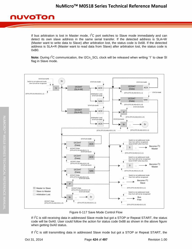
NuMicro M0518 Series Technical Reference Manual
Oct 31, 2014 Page 424 of 497 Revision 1.00
NU
MIC
RO
™ M
0518
SE
RIE
S T
EC
HN
ICA
L R
EF
ER
EN
CE
MA
NU
AL
If bus arbitration is lost in Master mode, I2C port switches to Slave mode immediately and can
detect its own slave address in the same serial transfer. If the detected address is SLA+W (Master want to write data to Slave) after arbitration lost, the status code is 0x68. If the detected address is SLA+R (Master want to read data from Slave) after arbitration lost, the status code is 0xB0.
Note: During I2C communication, the I2Cn_SCL clock will be released when writing ‘1’ to clear SI
flag in Slave mode.
S
(STA,STO,SI,AA)=(1,0,1,1)
... ...
Switch to not addressed mode
Own SLA will be recognized
Send START when bus free
S
(STA,STO,SI,AA)=(1,0,1,0)
... ...
Switch to not addressed mode
Own SLA will not be recognized
Send START when bus free
...
(STA,STO,SI,AA)=(0,0,1,0)
Switch to not addressed mode
Own SLA will not be recognized
Become I2C
Master
Become I2C
Master
Bus
Free
S
I2CDAT
(SLA+R)ACK
(STA,STO,SI,AA)=(0,0,1,1)
STATUS=0xA8
I2CDAT
(Data)ACK
I2CDAT=Data
(STA,STO,SI,AA)=(0,0,1,1)
...
I2CDAT
(Data)
I2CDAT=Data
(STA,STO,SI,AA)=(0,0,1,0)
STATUS=0xB8
Switch to not addressed modeOwn SLA will be recognized
ACK
I2CDAT
(Data)
I2CDAT=Data
(STA,STO,SI,AA)=(0,0,1,0)
NAK
STATUS=0xC8
STATUS=0xC0
ACK
(Arbitration Lost)
STATUS=0xB0
I2CDAT
(SLA+W)ACK
STATUS=0x60
I2CDAT
(Data)ACK
NAK
(STA,STO,SI,AA)=(0,0,1,1)
I2CDAT
(Data)
(STA,STO,SI,AA)=(0,0,1,0)
STATUS=0x80
STATUS=0x88
Arbitration Lost
Master to Slave
Slave to Master
STATUS=0xA0
NAK
(Arbitration Lost)
STATUS=0x68
P
Sr
Sr
P
STATUS=0xA0
Sr
...
(STA,STO,SI,AA)=(0,0,1,1)
Switch to not addressed mode
Own SLA will be recognized
Become I2C
Slave
STATUS=0xA0
STATUS=0xA0
Sr
I2CDAT=Data
(STA,STO,SI,AA)=(0,0,1,X)
I2CDAT=Data
(STA,STO,SI,AA)=(0,0,1,X)
...
(STA,STO,SI,AA)=(0,0,1,1)
... Sr
(STA,STO,SI,AA)=(0,0,1,1)(STA,STO,SI,AA)=(0,0,1,X)
(STA,STO,SI,AA)=(0,0,1,X)
STATUS=0xF8
Figure 6-117 Save Mode Control Flow
If I2C is still receiving data in addressed Slave mode but got a STOP or Repeat START, the status
code will be 0xA0. User could follow the action for status code 0x88 as shown in the above figure when getting 0xA0 status.
If I2C is still transmitting data in addressed Slave mode but got a STOP or Repeat START, the

NuMicro M0518 Series Technical Reference Manual
Oct 31, 2014 Page 425 of 497 Revision 1.00
NU
MIC
RO
™ M
0518
SE
RIE
S T
EC
HN
ICA
L R
EF
ER
EN
CE
MA
NU
AL
status code will be 0xA0. User could follow the action for status code 0xC8 as shown in the above figure when getting 0xA0 status.
Note: After slave gets status of 0x88, 0xC8, 0xC0 and 0xA0, slave can switch to not address mode and own SLA will not be recognized. If entering this status, slave will not receive any I
2C
signal or address from master. At this status, I2C should be reset to leave this status.
6.12.5.2.3 General Call (GC) Mode
If the GC(I2CADDRn [0]) bit is set, the I2C port hardware will respond to General Call address
(0x00). User can clear GC bit to disable general call function. When the GC bit is set and the I2C
in Slave mode, it can receive the general call address by 0x00 after master send general call address to I
2C bus, then it will follow status of GC mode.
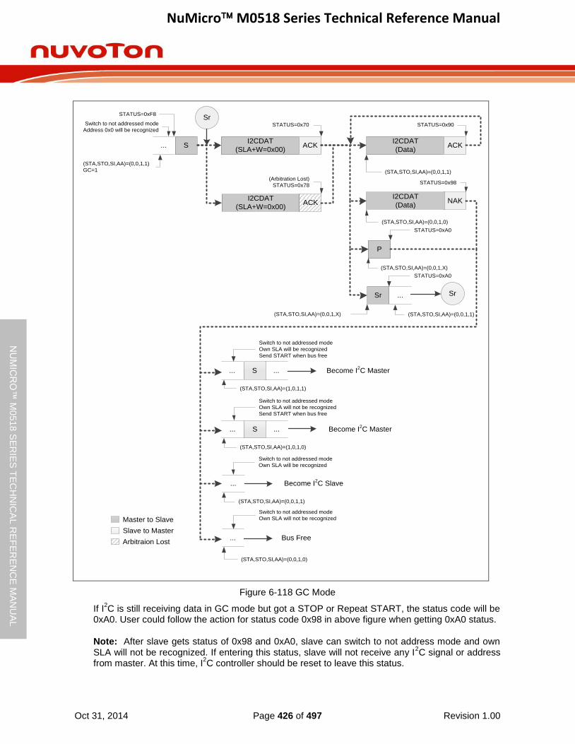
NuMicro M0518 Series Technical Reference Manual
Oct 31, 2014 Page 426 of 497 Revision 1.00
NU
MIC
RO
™ M
0518
SE
RIE
S T
EC
HN
ICA
L R
EF
ER
EN
CE
MA
NU
AL
SI2CDAT
(SLA+W=0x00)ACK
(STA,STO,SI,AA)=(0,0,1,1)
GC=1
STATUS=0x70
I2CDAT
(Data)ACK
NAK
(STA,STO,SI,AA)=(0,0,1,1)
...
I2CDAT
(Data)
(STA,STO,SI,AA)=(0,0,1,0)
STATUS=0x90
STATUS=0x98
S
(STA,STO,SI,AA)=(1,0,1,1)
... ...
Switch to not addressed mode
Own SLA will be recognized
Send START when bus free
S
(STA,STO,SI,AA)=(1,0,1,0)
... ...
Switch to not addressed mode
Own SLA will not be recognized
Send START when bus free
...
Switch to not addressed mode
Address 0x0 will be recognized
(STA,STO,SI,AA)=(0,0,1,0)
Switch to not addressed mode
Own SLA will not be recognized
Become I2C Master
Become I2C Master
Bus Free
...
(STA,STO,SI,AA)=(0,0,1,1)
Switch to not addressed mode
Own SLA will be recognized
Become I2C Slave
I2CDAT
(SLA+W=0x00)ACK
(Arbitration Lost)
STATUS=0x78
Arbitraion Lost
Master to Slave
Slave to Master
STATUS=0xA0
Sr
STATUS=0xA0
P
Sr
(STA,STO,SI,AA)=(0,0,1,1)
...
Sr
(STA,STO,SI,AA)=(0,0,1,X)
(STA,STO,SI,AA)=(0,0,1,X)
STATUS=0xF8
Figure 6-118 GC Mode
If I2C is still receiving data in GC mode but got a STOP or Repeat START, the status code will be
0xA0. User could follow the action for status code 0x98 in above figure when getting 0xA0 status.
Note: After slave gets status of 0x98 and 0xA0, slave can switch to not address mode and own SLA will not be recognized. If entering this status, slave will not receive any I
2C signal or address
from master. At this time, I2C controller should be reset to leave this status.
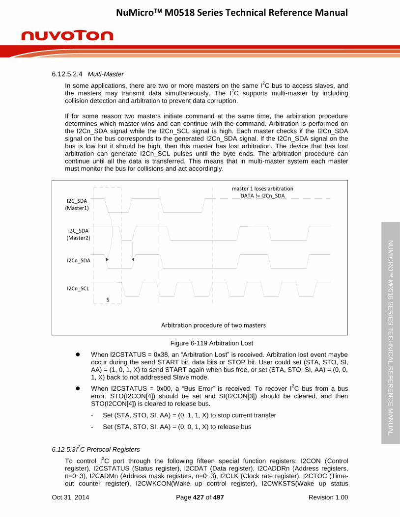
NuMicro M0518 Series Technical Reference Manual
Oct 31, 2014 Page 427 of 497 Revision 1.00
NU
MIC
RO
™ M
0518
SE
RIE
S T
EC
HN
ICA
L R
EF
ER
EN
CE
MA
NU
AL
6.12.5.2.4 Multi-Master
In some applications, there are two or more masters on the same I2C bus to access slaves, and
the masters may transmit data simultaneously. The I2C supports multi-master by including
collision detection and arbitration to prevent data corruption.
If for some reason two masters initiate command at the same time, the arbitration procedure determines which master wins and can continue with the command. Arbitration is performed on the I2Cn_SDA signal while the I2Cn_SCL signal is high. Each master checks if the I2Cn_SDA signal on the bus corresponds to the generated I2Cn_SDA signal. If the I2Cn_SDA signal on the bus is low but it should be high, then this master has lost arbitration. The device that has lost arbitration can generate I2Cn_SCL pulses until the byte ends. The arbitration procedure can continue until all the data is transferred. This means that in multi-master system each master must monitor the bus for collisions and act accordingly.
I2C_SDA(Master1)
I2Cn_SDA
I2Cn_SCL
S
master 1 loses arbitration DATA != I2Cn_SDA
Arbitration procedure of two masters
I2C_SDA(Master2)
Figure 6-119 Arbitration Lost
When I2CSTATUS = 0x38, an “Arbitration Lost” is received. Arbitration lost event maybe occur during the send START bit, data bits or STOP bit. User could set (STA, STO, SI, AA) = (1, 0, 1, X) to send START again when bus free, or set (STA, STO, SI, AA) = (0, 0, 1, X) back to not addressed Slave mode.
When I2CSTATUS = 0x00, a “Bus Error” is received. To recover I2C bus from a bus
error, STO(I2CON[4]) should be set and SI(I2CON[3]) should be cleared, and then STO(I2CON[4]) is cleared to release bus.
- Set (STA, STO, SI, AA) = (0, 1, 1, X) to stop current transfer
- Set (STA, STO, SI, AA) = (0, 0, 1, X) to release bus
6.12.5.3 I2C Protocol Registers
To control I2C port through the following fifteen special function registers: I2CON (Control
register), I2CSTATUS (Status register), I2CDAT (Data register), I2CADDRn (Address registers, n=0~3), I2CADMn (Address mask registers, n=0~3), I2CLK (Clock rate register), I2CTOC (Time-out counter register), I2CWKCON(Wake up control register), I2CWKSTS(Wake up status

NuMicro M0518 Series Technical Reference Manual
Oct 31, 2014 Page 428 of 497 Revision 1.00
NU
MIC
RO
™ M
0518
SE
RIE
S T
EC
HN
ICA
L R
EF
ER
EN
CE
MA
NU
AL
register).
6.12.5.3.1 Address Registers (I2CADDR)
The I2C port is equipped with four slave address registers, I2CADDRn (n=0~3). The contents of
the register are irrelevant when I2C is in Master mode. In Slave mode, the bit field I2CADDRn[7:1]
must be loaded with the chip’s own slave address. The I2C hardware will react if the contents of
I2CADDRn are matched with the received slave address.
The I2C ports support the “General Call” function. If the GC (I2CADDRn [0]) bit is set the I
2C port
hardware will respond to General Call address (0x00). Clear GC bit to disable general call function.
When the GC bit is set and the I2C is in Slave mode, it can receive the general call address by
0x00 after Master send general call address to I2C bus, then it will follow status of GC mode.
6.12.5.3.2 Slave Address Mask Registers (I2CADM)
The I2C bus controller supports multiple address recognition with four address mask registers
I2CADMn (n=0~3). When the bit in the address mask register is set to 1, it means the received corresponding address bit is "Don’t care". If the bit is set to 0, it means the received corresponding register bit should be exactly the same as address register.
6.12.5.3.3 Data Register (I2CDAT)
This register contains a byte of serial data to be transmitted or a byte which just has been received. The CPU can be read from or written to the 8-bit (I2CDAT [7:0]) directly while it is not in the process of shifting a byte. When I
2C is in a defined state and the SI (I2CON[3]) is set, data in
I2CDAT [7:0] remains stable. While data is being shifted out, data on the bus is simultaneously being shifted in; I2CDAT [7:0] always contains the last data byte presented on the bus.
The acknowledge bit is controlled by the I2C hardware and cannot be accessed by the CPU.
Serial data is shifted into I2CDAT [7:0] on the rising edges of serial clock pulses on the I2Cn_SCL line. When a byte has been shifted into I2CDAT [7:0], the serial data is available in I2CDAT [7:0], and the acknowledge bit (ACK or NACK) is returned by the control logic during the ninth clock pulse. In order to monitor bus status while sending data, the bus date will be shifted to I2CDAT[7:0] when sending I2CDAT[7:0] to bus. In the case of sending data, serial data bits are shifted out from I2CDAT [7:0] on the falling edge of I2Cn_SCL clocks, and is shifted to I2CDAT [7:0] on the rising edge of I2Cn_SCL clocks.
I2DAT.7 I2DAT.6 I2DAT.5 I2DAT.4 I2DAT.3 I2DAT.2 I2DAT.1 I2DAT.0
I2C Data Register:
shifting direction
Figure 6-120 I2C Data Shifting Direction
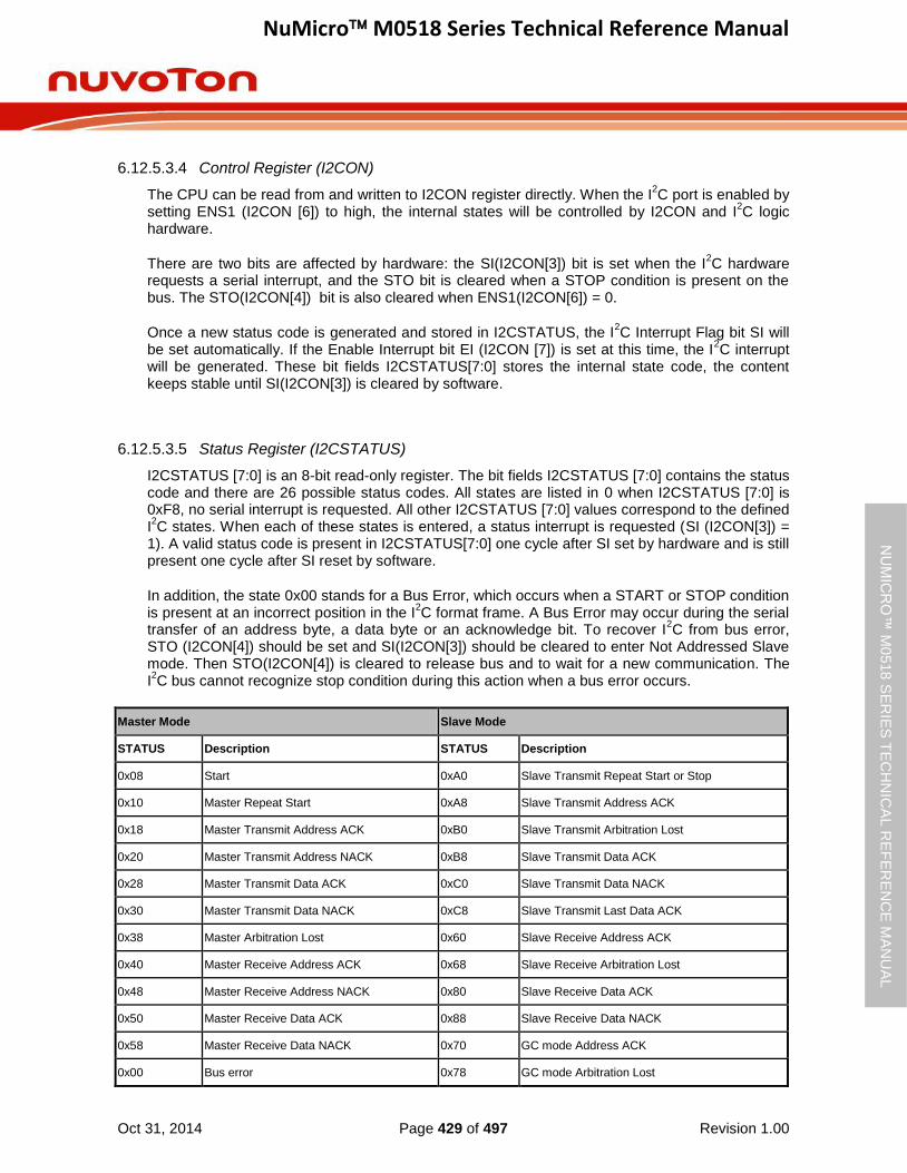
NuMicro M0518 Series Technical Reference Manual
Oct 31, 2014 Page 429 of 497 Revision 1.00
NU
MIC
RO
™ M
0518
SE
RIE
S T
EC
HN
ICA
L R
EF
ER
EN
CE
MA
NU
AL
6.12.5.3.4 Control Register (I2CON)
The CPU can be read from and written to I2CON register directly. When the I2C port is enabled by
setting ENS1 (I2CON [6]) to high, the internal states will be controlled by I2CON and I2C logic
hardware.
There are two bits are affected by hardware: the SI(I2CON[3]) bit is set when the I2C hardware
requests a serial interrupt, and the STO bit is cleared when a STOP condition is present on the bus. The STO(I2CON[4]) bit is also cleared when ENS1(I2CON[6]) = 0.
Once a new status code is generated and stored in I2CSTATUS, the I2C Interrupt Flag bit SI will
be set automatically. If the Enable Interrupt bit EI (I2CON [7]) is set at this time, the I2C interrupt
will be generated. These bit fields I2CSTATUS[7:0] stores the internal state code, the content keeps stable until SI(I2CON[3]) is cleared by software.
6.12.5.3.5 Status Register (I2CSTATUS)
I2CSTATUS [7:0] is an 8-bit read-only register. The bit fields I2CSTATUS [7:0] contains the status code and there are 26 possible status codes. All states are listed in 0 when I2CSTATUS [7:0] is 0xF8, no serial interrupt is requested. All other I2CSTATUS [7:0] values correspond to the defined I2C states. When each of these states is entered, a status interrupt is requested (SI (I2CON[3]) =
1). A valid status code is present in I2CSTATUS[7:0] one cycle after SI set by hardware and is still present one cycle after SI reset by software.
In addition, the state 0x00 stands for a Bus Error, which occurs when a START or STOP condition is present at an incorrect position in the I
2C format frame. A Bus Error may occur during the serial
transfer of an address byte, a data byte or an acknowledge bit. To recover I2C from bus error,
STO (I2CON[4]) should be set and SI(I2CON[3]) should be cleared to enter Not Addressed Slave mode. Then STO(I2CON[4]) is cleared to release bus and to wait for a new communication. The I2C bus cannot recognize stop condition during this action when a bus error occurs.
Master Mode Slave Mode
STATUS Description STATUS Description
0x08 Start 0xA0 Slave Transmit Repeat Start or Stop
0x10 Master Repeat Start 0xA8 Slave Transmit Address ACK
0x18 Master Transmit Address ACK 0xB0 Slave Transmit Arbitration Lost
0x20 Master Transmit Address NACK 0xB8 Slave Transmit Data ACK
0x28 Master Transmit Data ACK 0xC0 Slave Transmit Data NACK
0x30 Master Transmit Data NACK 0xC8 Slave Transmit Last Data ACK
0x38 Master Arbitration Lost 0x60 Slave Receive Address ACK
0x40 Master Receive Address ACK 0x68 Slave Receive Arbitration Lost
0x48 Master Receive Address NACK 0x80 Slave Receive Data ACK
0x50 Master Receive Data ACK 0x88 Slave Receive Data NACK
0x58 Master Receive Data NACK 0x70 GC mode Address ACK
0x00 Bus error 0x78 GC mode Arbitration Lost
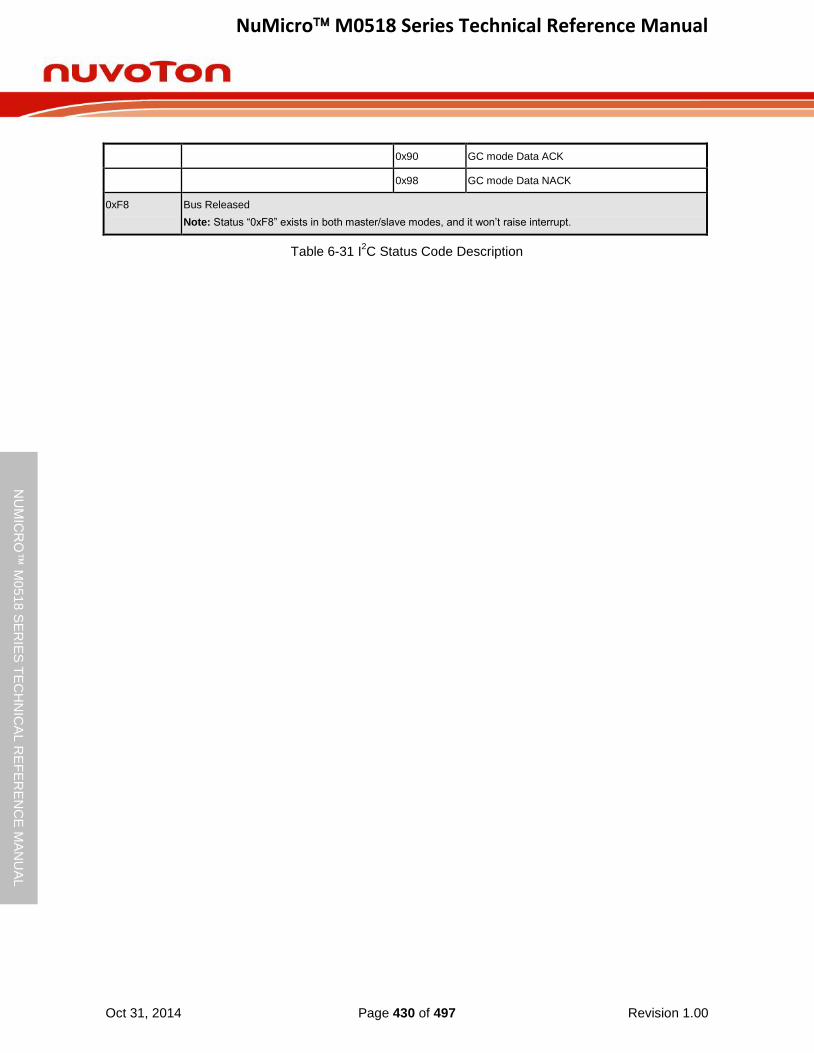
NuMicro M0518 Series Technical Reference Manual
Oct 31, 2014 Page 430 of 497 Revision 1.00
NU
MIC
RO
™ M
0518
SE
RIE
S T
EC
HN
ICA
L R
EF
ER
EN
CE
MA
NU
AL
0x90 GC mode Data ACK
0x98 GC mode Data NACK
0xF8 Bus Released
Note: Status “0xF8” exists in both master/slave modes, and it won’t raise interrupt.
Table 6-31 I2C Status Code Description
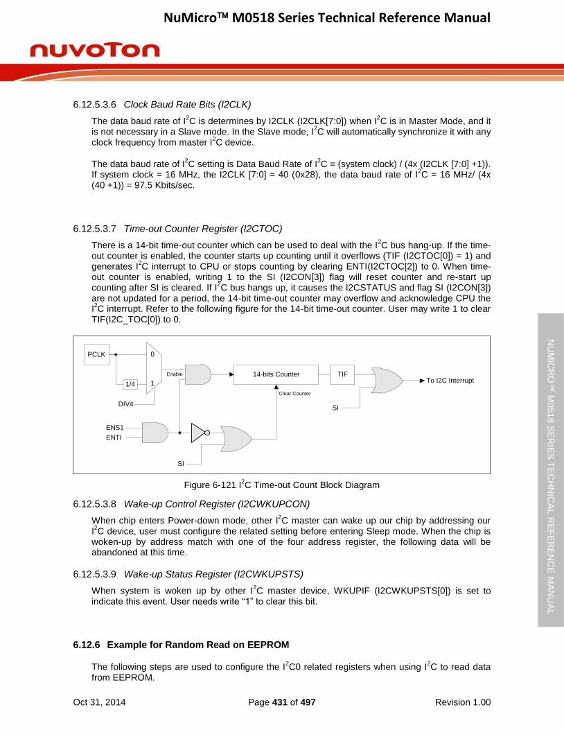
NuMicro M0518 Series Technical Reference Manual
Oct 31, 2014 Page 431 of 497 Revision 1.00
NU
MIC
RO
™ M
0518
SE
RIE
S T
EC
HN
ICA
L R
EF
ER
EN
CE
MA
NU
AL
6.12.5.3.6 Clock Baud Rate Bits (I2CLK)
The data baud rate of I2C is determines by I2CLK (I2CLK[7:0]) when I
2C is in Master Mode, and it
is not necessary in a Slave mode. In the Slave mode, I2C will automatically synchronize it with any
clock frequency from master I2C device.
The data baud rate of I2C setting is Data Baud Rate of I
2C = (system clock) / (4x (I2CLK [7:0] +1)).
If system clock = 16 MHz, the I2CLK [7:0] = 40 (0x28), the data baud rate of I2C = 16 MHz/ (4x
(40 +1)) = 97.5 Kbits/sec.
6.12.5.3.7 Time-out Counter Register (I2CTOC)
There is a 14-bit time-out counter which can be used to deal with the I2C bus hang-up. If the time-
out counter is enabled, the counter starts up counting until it overflows (TIF (I2CTOC[0]) = 1) and generates I
2C interrupt to CPU or stops counting by clearing ENTI(I2CTOC[2]) to 0. When time-
out counter is enabled, writing 1 to the SI (I2CON[3]) flag will reset counter and re-start up counting after SI is cleared. If I
2C bus hangs up, it causes the I2CSTATUS and flag SI (I2CON[3])
are not updated for a period, the 14-bit time-out counter may overflow and acknowledge CPU the I2C interrupt. Refer to the following figure for the 14-bit time-out counter. User may write 1 to clear
TIF(I2C_TOC[0]) to 0.
1
0PCLK
1/4
14-bits Counter TIF
Clear Counter
ENTI
SIDIV4
ENS1
To I2C InterruptEnable
SI
Figure 6-121 I2C Time-out Count Block Diagram
6.12.5.3.8 Wake-up Control Register (I2CWKUPCON)
When chip enters Power-down mode, other I2C master can wake up our chip by addressing our
I2C device, user must configure the related setting before entering Sleep mode. When the chip is
woken-up by address match with one of the four address register, the following data will be abandoned at this time.
6.12.5.3.9 Wake-up Status Register (I2CWKUPSTS)
When system is woken up by other I2C master device, WKUPIF (I2CWKUPSTS[0]) is set to
indicate this event. User needs write “1” to clear this bit.
6.12.6 Example for Random Read on EEPROM
The following steps are used to configure the I2C0 related registers when using I
2C to read data
from EEPROM.

NuMicro M0518 Series Technical Reference Manual
Oct 31, 2014 Page 432 of 497 Revision 1.00
NU
MIC
RO
™ M
0518
SE
RIE
S T
EC
HN
ICA
L R
EF
ER
EN
CE
MA
NU
AL
1. Set the multi-function pin in the “GPA_MFP” registers as I2C0_SCL and I2C0_SDA pins.
2. Enable I2C APB clock by setting I2C0_EN (APBCLK[8]).
3. Set I2C0_RST (IPRSTC2 [8]) = 1 to reset I2C controller then set I
2C controller to normal
operation by setting I2C0_RST (IPRSTC2 [8]) = 0;
4. Set ENS1 (I2CON[6])=1 to enable I2C0 controller.
5. Write a divided value by setting I2CLK register for I2C clock rate.
6. Set SETENA (NVIC_ISER[31:0])=0x00040000 in the “NVIC_ISER” register to set I2C0
IRQ.
7. Set EI (I2CON[7])=1 to enable I2C0 Interrupt.
8. Set I2C0 address registers which are “I2CADDR0~I2CADDR3”.
Random read operation is one of the methods of access EEPROM. The method allows the master to access any address of EEPROM space. The following figure shows the EEPROM
random read operation.
S
T
A
1 0 1 0A
2
A
1
A
0W
A
C
K
X X X
A
C
K
A
C
K
S
T1 0 1 0
A
2
A
1
A
0R
A
C
K
N
A
C
K
S
T
O
DATA BYTEROM ADDRRSS
LOW BYTE
ROM ADDRRSS
HIGH BYTESLA+W
I2Cn_SDA
SLA+R
Figure 6-122 EEPROM Random Read
The following figure shows how to use I2C controller to implement the protocol of EEPROM
random read.
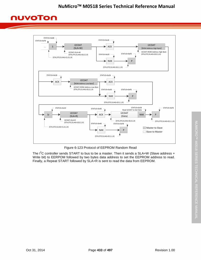
NuMicro M0518 Series Technical Reference Manual
Oct 31, 2014 Page 433 of 497 Revision 1.00
NU
MIC
RO
™ M
0518
SE
RIE
S T
EC
HN
ICA
L R
EF
ER
EN
CE
MA
NU
AL
SI2CDAT
(SLA+W)ACK
Master to Slave
Slave to Master
I2CDAT(ROM Address High Byte)
ACK
SrI2CDAT(SLA+R)
ACK
P
STATUS=0x08
(STA,STO,SI,AA)=(1,0,1,X)
STATUS=0x18
I2CDAT=SLA+W(STA,STO,SI,AA)=(0,0,1,X)
STATUS=0x28
I2CDAT=ROM Address High Byte(STA,STO,SI,AA)=(0,0,1,X)
STATUS=0x10
(STA,STO,SI,AA)=(1,0,1,X)
STATUS=0xF8
(STA,STO,SI,AA)=(0,1,1,X)
I2CDAT=SLA+R(STA,STO,SI,AA)=(0,0,1,X)
STATUS=0x40
NAK
STATUS=0x20
I2CDAT(ROM Address Low Byte)
ACK
STATUS=0x28
I2CDAT=ROM Address Low Byte(STA,STO,SI,AA)=(0,0,1,X)
P
STATUS=0xF8
(STA,STO,SI,AA)=(0,1,1,X)
NAK
STATUS=0x30
I2CDAT(Data)
NAK
STATUS=0x58Read I2CDAT to Get Data
(STA,STO,SI,AA)=(0,0,1,0)
P
STATUS=0xF8
(STA,STO,SI,AA)=(0,1,1,X)
NAK
STATUS=0x48
P
STATUS=0xF8
(STA,STO,SI,AA)=(0,1,1,X)
...
STATUS=0xF8
Figure 6-123 Protocol of EEPROM Random Read
The I2C controller sends START to bus to be a master. Then it sends a SLA+W (Slave address +
Write bit) to EERPOM followed by two bytes data address to set the EEPROM address to read. Finally, a Repeat START followed by SLA+R is sent to read the data from EEPROM.
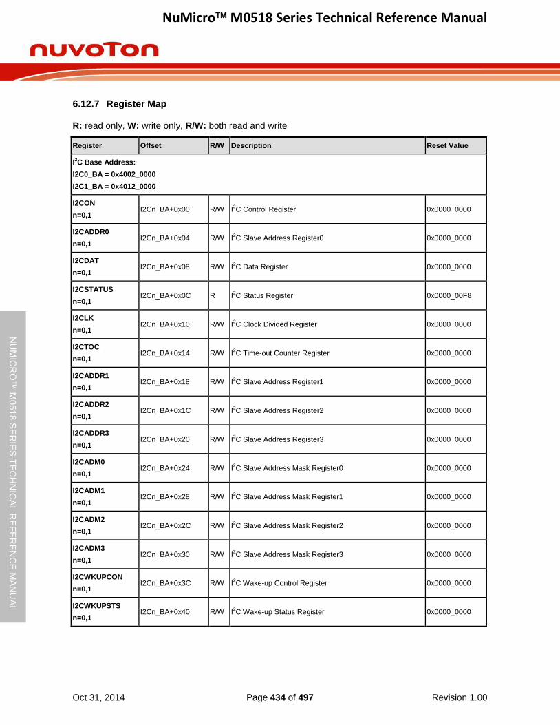
NuMicro M0518 Series Technical Reference Manual
Oct 31, 2014 Page 434 of 497 Revision 1.00
NU
MIC
RO
™ M
0518
SE
RIE
S T
EC
HN
ICA
L R
EF
ER
EN
CE
MA
NU
AL
6.12.7 Register Map
R: read only, W: write only, R/W: both read and write
Register Offset R/W Description Reset Value
I2C Base Address:
I2C0_BA = 0x4002_0000
I2C1_BA = 0x4012_0000
I2CON
n=0,1 I2Cn_BA+0x00 R/W I
2C Control Register 0x0000_0000
I2CADDR0
n=0,1 I2Cn_BA+0x04 R/W I
2C Slave Address Register0 0x0000_0000
I2CDAT
n=0,1 I2Cn_BA+0x08 R/W I
2C Data Register 0x0000_0000
I2CSTATUS
n=0,1 I2Cn_BA+0x0C R I
2C Status Register 0x0000_00F8
I2CLK
n=0,1 I2Cn_BA+0x10 R/W I
2C Clock Divided Register 0x0000_0000
I2CTOC
n=0,1 I2Cn_BA+0x14 R/W I
2C Time-out Counter Register 0x0000_0000
I2CADDR1
n=0,1 I2Cn_BA+0x18 R/W I
2C Slave Address Register1 0x0000_0000
I2CADDR2
n=0,1 I2Cn_BA+0x1C R/W I
2C Slave Address Register2 0x0000_0000
I2CADDR3
n=0,1 I2Cn_BA+0x20 R/W I
2C Slave Address Register3 0x0000_0000
I2CADM0
n=0,1 I2Cn_BA+0x24 R/W I
2C Slave Address Mask Register0 0x0000_0000
I2CADM1
n=0,1 I2Cn_BA+0x28 R/W I
2C Slave Address Mask Register1 0x0000_0000
I2CADM2
n=0,1 I2Cn_BA+0x2C R/W I
2C Slave Address Mask Register2 0x0000_0000
I2CADM3
n=0,1 I2Cn_BA+0x30 R/W I
2C Slave Address Mask Register3 0x0000_0000
I2CWKUPCON
n=0,1 I2Cn_BA+0x3C R/W I
2C Wake-up Control Register 0x0000_0000
I2CWKUPSTS
n=0,1 I2Cn_BA+0x40 R/W I
2C Wake-up Status Register 0x0000_0000

NuMicro M0518 Series Technical Reference Manual
Oct 31, 2014 Page 435 of 497 Revision 1.00
NU
MIC
RO
™ M
0518
SE
RIE
S T
EC
HN
ICA
L R
EF
ER
EN
CE
MA
NU
AL
6.12.8 Register Description
I2C Control Register (I2CON)
Register Offset R/W Description Reset Value
I2CON
n=0,1 I2Cn_BA+0x00 R/W I
2C Control Register 0x0000_0000
31 30 29 28 27 26 25 24
Reserved
23 22 21 20 19 18 17 16
Reserved
15 14 13 12 11 10 9 8
Reserved
7 6 5 4 3 2 1 0
EI ENS1 STA STO SI AA Reserved
Bits Description
[31:8] Reserved Reserved.
[7] EI
Interrupt Enable Coontrol
0 = I2C interrupt Disabled.
1 = I2C interrupt Enabled.
[6] ENS1
I2C Controller Enable Coontrol
0 = Disabled.
1 = Enabled.
Set to enable I2C serial function controller. When ENS1=1 the I
2C serial function enables.
The multi-function pin function of I2Cn_SDA and I2Cn_SCL must set to I2C function first.
[5] STA
I2C START Control
Setting STA to logic 1 to enter Master mode, the I2C hardware sends a START or repeat
START condition to bus when the bus is free.
[4] STO
I2C STOP Control
In Master mode, setting STO to transmit a STOP condition to bus then I2C hardware will
check the bus condition if a STOP condition is detected this bit will be cleared by hardware automatically. In a slave mode, setting STO resets I
2C hardware to the defined “not
addressed” slave mode. This means it is NO LONGER in the slave receiver mode to receive data from the master transmit device.
[3] SI
I2C Interrupt Flag
When a new I2C state is present in the I2CSTATUS register, the SI flag is set by hardware,
and if bit EI (I2CON [7]) is set, the I2C interrupt is requested. SI must be cleared by
software. Clear SI by writing 1 to this bit.
[2] AA
Assert Acknowledge Control
When AA =1 prior to address or data received, an acknowledged (low level to I2Cn_SDA) will be returned during the acknowledge clock pulse on the I2Cn_SCL line when 1.) A slave is acknowledging the address sent from master, 2.) The receiver devices are acknowledging the data sent by transmitter. When AA=0 prior to address or data received,
NuMicro M0518 Series Technical Reference Manual
Oct 31, 2014 Page 436 of 497 Revision 1.00
NU
MIC
RO
™ M
0518
SE
RIE
S T
EC
HN
ICA
L R
EF
ER
EN
CE
MA
NU
AL
a Not acknowledged (high level to I2Cn_SDA) will be returned during the acknowledge clock pulse on the I2Cn_SCL line.
[1:0] Reserved Reserved.
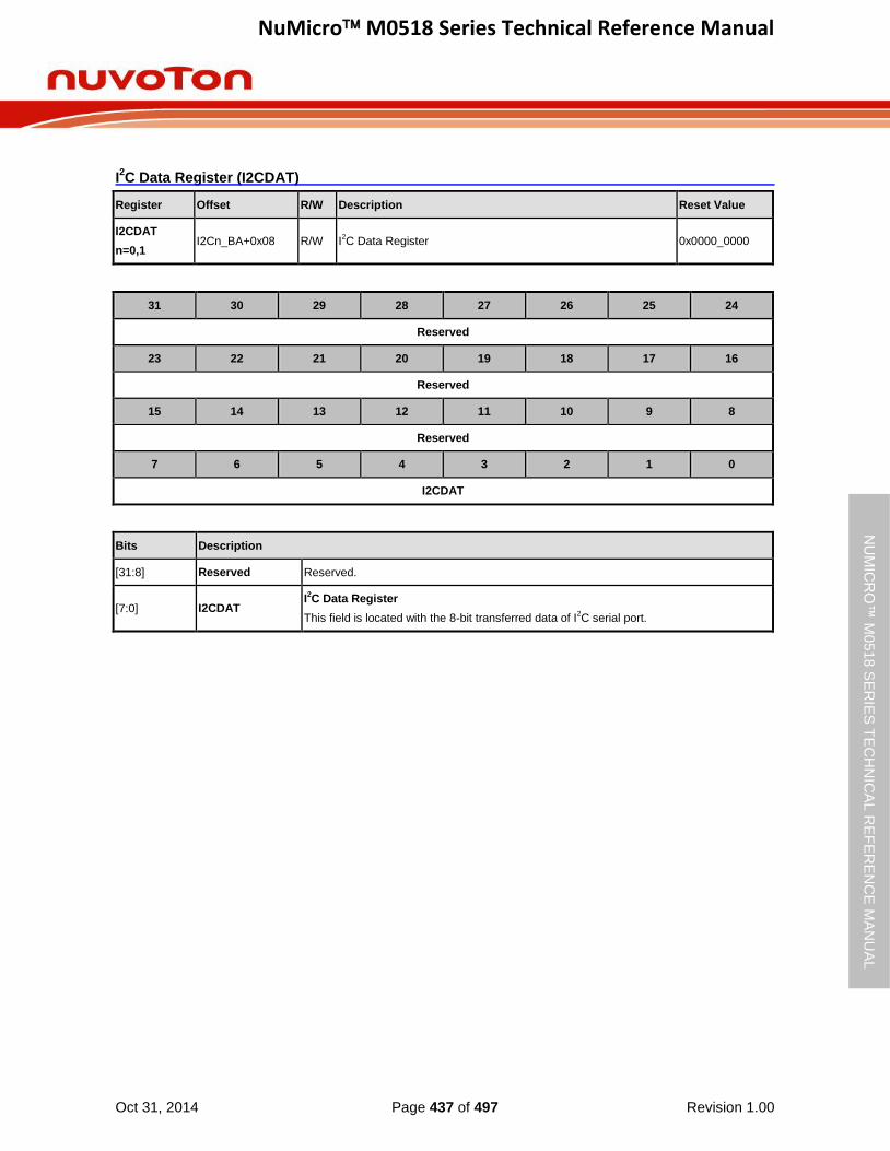
NuMicro M0518 Series Technical Reference Manual
Oct 31, 2014 Page 437 of 497 Revision 1.00
NU
MIC
RO
™ M
0518
SE
RIE
S T
EC
HN
ICA
L R
EF
ER
EN
CE
MA
NU
AL
I2C Data Register (I2CDAT)
Register Offset R/W Description Reset Value
I2CDAT
n=0,1 I2Cn_BA+0x08 R/W I
2C Data Register 0x0000_0000
31 30 29 28 27 26 25 24
Reserved
23 22 21 20 19 18 17 16
Reserved
15 14 13 12 11 10 9 8
Reserved
7 6 5 4 3 2 1 0
I2CDAT
Bits Description
[31:8] Reserved Reserved.
[7:0] I2CDAT I2C Data Register
This field is located with the 8-bit transferred data of I2C serial port.
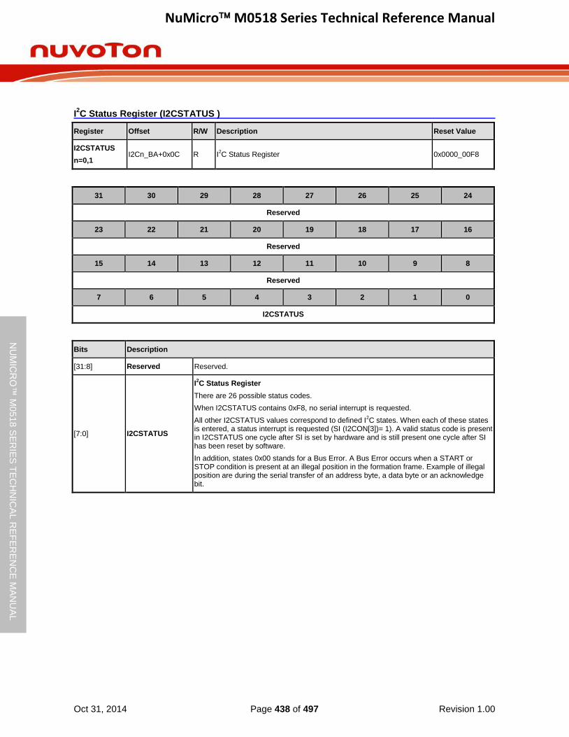
NuMicro M0518 Series Technical Reference Manual
Oct 31, 2014 Page 438 of 497 Revision 1.00
NU
MIC
RO
™ M
0518
SE
RIE
S T
EC
HN
ICA
L R
EF
ER
EN
CE
MA
NU
AL
I2C Status Register (I2CSTATUS )
Register Offset R/W Description Reset Value
I2CSTATUS
n=0,1 I2Cn_BA+0x0C R I
2C Status Register 0x0000_00F8
31 30 29 28 27 26 25 24
Reserved
23 22 21 20 19 18 17 16
Reserved
15 14 13 12 11 10 9 8
Reserved
7 6 5 4 3 2 1 0
I2CSTATUS
Bits Description
[31:8] Reserved Reserved.
[7:0] I2CSTATUS
I2C Status Register
There are 26 possible status codes.
When I2CSTATUS contains 0xF8, no serial interrupt is requested.
All other I2CSTATUS values correspond to defined I2C states. When each of these states
is entered, a status interrupt is requested (SI (I2CON[3])= 1). A valid status code is present in I2CSTATUS one cycle after SI is set by hardware and is still present one cycle after SI has been reset by software.
In addition, states 0x00 stands for a Bus Error. A Bus Error occurs when a START or STOP condition is present at an illegal position in the formation frame. Example of illegal position are during the serial transfer of an address byte, a data byte or an acknowledge bit.

NuMicro M0518 Series Technical Reference Manual
Oct 31, 2014 Page 439 of 497 Revision 1.00
NU
MIC
RO
™ M
0518
SE
RIE
S T
EC
HN
ICA
L R
EF
ER
EN
CE
MA
NU
AL
I2C Clock Divided Register (I2CLK)
Register Offset R/W Description Reset Value
I2CLK
n=0,1 I2Cn_BA+0x10 R/W I
2C Clock Divided Register 0x0000_0000
31 30 29 28 27 26 25 24
Reserved
23 22 21 20 19 18 17 16
Reserved
15 14 13 12 11 10 9 8
Reserved
7 6 5 4 3 2 1 0
I2CLK
Bits Description
[31:8] Reserved Reserved.
[7:0] I2CLK
I2C Clock Divided Register
The I2C clock rate bits: Data Baud Rate of I
2C = (system clock) / (4 * (I2CLK+1)).
Note: The minimum value of I2CLK is 4.

NuMicro M0518 Series Technical Reference Manual
Oct 31, 2014 Page 440 of 497 Revision 1.00
NU
MIC
RO
™ M
0518
SE
RIE
S T
EC
HN
ICA
L R
EF
ER
EN
CE
MA
NU
AL
I2C Time-out Counter Register (I2CTOC)
Register Offset R/W Description Reset Value
I2CTOC
n=0,1 I2Cn_BA+0x14 R/W I
2C Time-out Counter Register 0x0000_0000
31 30 29 28 27 26 25 24
Reserved
23 22 21 20 19 18 17 16
Reserved
15 14 13 12 11 10 9 8
Reserved
7 6 5 4 3 2 1 0
Reserved ENTI DIV4 TIF
Bits Description
[31:3] Reserved Reserved.
[2] ENTI
Time-Out Counter Enable Coontrol
0 = Disabled.
1 = Enabled.
When Enabled, the 14-bit time-out counter will start counting when SI (I2CON[3]) is clear. Setting flag SI SI(I2CON[3]) to high will reset counter and re-start up counting after SI SI(I2CON[3]) is cleared.
[1] DIV4
Time-Out Counter Input Clock Divided By 4
0 = Disabled.
1 = Enabled.
When Enabled, The time-out period is extend 4 times.
[0] TIF
Time-Out Flag
This bit is set by hardware when I2C time-out happened and it can interrupt CPU if I
2C
interrupt enable bit EI (I2CON[7]) is set to 1.
Note: Write 1 to clear this bit.
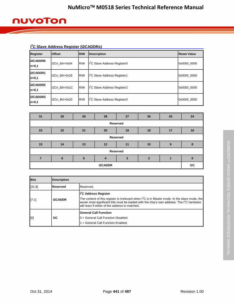
NuMicro M0518 Series Technical Reference Manual
Oct 31, 2014 Page 441 of 497 Revision 1.00
NU
MIC
RO
™ M
0518
SE
RIE
S T
EC
HN
ICA
L R
EF
ER
EN
CE
MA
NU
AL
I2C Slave Address Register (I2CADDRx)
Register Offset R/W Description Reset Value
I2CADDR0
n=0,1 I2Cn_BA+0x04 R/W I
2C Slave Address Register0 0x0000_0000
I2CADDR1
n=0,1 I2Cn_BA+0x18 R/W I
2C Slave Address Register1 0x0000_0000
I2CADDR2
n=0,1 I2Cn_BA+0x1C R/W I
2C Slave Address Register2 0x0000_0000
I2CADDR3
n=0,1 I2Cn_BA+0x20 R/W I
2C Slave Address Register3 0x0000_0000
31 30 29 28 27 26 25 24
Reserved
23 22 21 20 19 18 17 16
Reserved
15 14 13 12 11 10 9 8
Reserved
7 6 5 4 3 2 1 0
I2CADDR GC
Bits Description
[31:8] Reserved Reserved.
[7:1] I2CADDR
I2C Address Register
The content of this register is irrelevant when I2C is in Master mode. In the slave mode, the
seven most significant bits must be loaded with the chip’s own address. The I2C hardware
will react if either of the address is matched.
[0] GC
General Call Function
0 = General Call Function Disabled.
1 = General Call Function Enabled.

NuMicro M0518 Series Technical Reference Manual
Oct 31, 2014 Page 442 of 497 Revision 1.00
NU
MIC
RO
™ M
0518
SE
RIE
S T
EC
HN
ICA
L R
EF
ER
EN
CE
MA
NU
AL
I2C Slave Address Mask Register (I2CADMx)
Register Offset R/W Description Reset Value
I2CADM0
n=0,1 I2Cn_BA+0x24 R/W I
2C Slave Address Mask Register0 0x0000_0000
I2CADM1
n=0,1 I2Cn_BA+0x28 R/W I
2C Slave Address Mask Register1 0x0000_0000
I2CADM2
n=0,1 I2Cn_BA+0x2C R/W I
2C Slave Address Mask Register2 0x0000_0000
I2CADM3
n=0,1 I2Cn_BA+0x30 R/W I
2C Slave Address Mask Register3 0x0000_0000
31 30 29 28 27 26 25 24
Reserved
23 22 21 20 19 18 17 16
Reserved
15 14 13 12 11 10 9 8
Reserved
7 6 5 4 3 2 1 0
I2CADM Reserved
Bits Description
[31:8] Reserved Reserved.
[7:1] I2CADM
I2C Address Mask Register
0 = Mask Disabled (the received corresponding register bit should be exact the same as address register.).
1 = Mask Enabled (the received corresponding address bit is don’t care.).
I2C bus controllers support multiple address recognition with four address mask register.
When the bit in the address mask register is set to one, it means the received corresponding address bit is don’t-care. If the bit is set to zero, that means the received corresponding register bit should be exact the same as address register.
[0] Reserved Reserved.
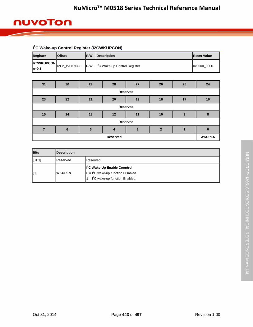
NuMicro M0518 Series Technical Reference Manual
Oct 31, 2014 Page 443 of 497 Revision 1.00
NU
MIC
RO
™ M
0518
SE
RIE
S T
EC
HN
ICA
L R
EF
ER
EN
CE
MA
NU
AL
I2C Wake-up Control Register (I2CWKUPCON)
Register Offset R/W Description Reset Value
I2CWKUPCON
n=0,1 I2Cn_BA+0x3C R/W I
2C Wake-up Control Register 0x0000_0000
31 30 29 28 27 26 25 24
Reserved
23 22 21 20 19 18 17 16
Reserved
15 14 13 12 11 10 9 8
Reserved
7 6 5 4 3 2 1 0
Reserved WKUPEN
Bits Description
[31:1] Reserved Reserved.
[0] WKUPEN
I2C Wake-Up Enable Coontrol
0 = I2C wake-up function Disabled.
1 = I2C wake-up function Enabled.

NuMicro M0518 Series Technical Reference Manual
Oct 31, 2014 Page 444 of 497 Revision 1.00
NU
MIC
RO
™ M
0518
SE
RIE
S T
EC
HN
ICA
L R
EF
ER
EN
CE
MA
NU
AL
I2C Wake-up Status Register (I2CWKUPSTS)
Register Offset R/W Description Reset Value
I2CWKUPSTS
n=0,1 I2Cn_BA+0x40 R/W I
2C Wake-up Status Register 0x0000_0000
31 30 29 28 27 26 25 24
Reserved
23 22 21 20 19 18 17 16
Reserved
15 14 13 12 11 10 9 8
Reserved
7 6 5 4 3 2 1 0
Reserved WKUPIF
Bits Description
[31:1] Reserved Reserved.
[0] WKUPIF
I2C Wake-Up Flag
0 = Chip is not woken-up from Power-down mode by I2C.
1 = Chip is woken-up from Power-down mode by I2C.
Note: Software can write 1 to clear this bit.

NuMicro M0518 Series Technical Reference Manual
Oct 31, 2014 Page 445 of 497 Revision 1.00
NU
MIC
RO
™ M
0518
SE
RIE
S T
EC
HN
ICA
L R
EF
ER
EN
CE
MA
NU
AL
6.13 Serial Peripheral Interface (SPI)
6.13.1 Overview
The Serial Peripheral Interface (SPI) is a synchronous serial data communication protocol that operates in full duplex mode. Devices communicate in Master/Slave mode with the 4-wire bi-
direction interface. The NuMicro M0518 series contains one set of SPI controllers performing a serial-to-parallel conversion on data received from a peripheral device, and a parallel-to-serial conversion on data transmitted to a peripheral device. This SPI controller can be configured as a master or a slave device.
The SPI controller supports the variable bus clock function for special applications.
6.13.2 Features
One set of SPI controller
Supports Master or Slave mode operation
Supports Dual I/O Transfer mode
Configurable bit length of a transaction word from 8 to 32 bits
Provides separate 8-layer depth transmit and receive FIFO buffers
Supports MSB first or LSB first transfer sequence
Supports the Byte Reorder function
Supports Byte or Word Suspend mode
Variable output bus clock frequency in Master mode
Supports 3-wire, no slave select signal, bi-direction interface

NuMicro M0518 Series Technical Reference Manual
Oct 31, 2014 Page 446 of 497 Revision 1.00
NU
MIC
RO
™ M
0518
SE
RIE
S T
EC
HN
ICA
L R
EF
ER
EN
CE
MA
NU
AL
6.13.3 Block Diagram
APB
Interface
Control
Status/Control
Register
Core Logic
8 Level TX Buffer
8 Level RX Buffer
Pad MUX
I/O
SPI0_MISO0
SPI0_MOSI0
SPI0_CLK
SPI0_SS0
SYNC
Control
Gray
Codec
Peripheral Clock
Figure 6-124 SPI Block Diagram
6.13.4 Basic Configuration
The basic configurations of SPI0 are as follows:
SPI0 pin functions are configured in ALT_MFP, GPB_MFP and GPC_MFP registers.
Select the source of SPI0 peripheral clock on SPI0_S (CLKSEL1[4]).
Enable SPI0 peripheral clock on SPI0_EN (APBCLK[12]).
Reset SPI0 controller on SPI0_RST (IPRSC2[12]).

NuMicro M0518 Series Technical Reference Manual
Oct 31, 2014 Page 447 of 497 Revision 1.00
NU
MIC
RO
™ M
0518
SE
RIE
S T
EC
HN
ICA
L R
EF
ER
EN
CE
MA
NU
AL
6.13.5 Functional Description
6.13.5.1 Terminology
SPI Peripheral Clock and SPI Bus Clock
The SPI controller needs the SPI peripheral clock to drive the SPI logic unit to perform the data transfer. The SPI bus clock is the clock presented on SPI0_CLK pin.
The SPI peripheral clock rate is determined by the settings of clock source, BCn option and clock divisor. The SPI0_S bit of CLKSEL1 register determines the clock source of the SPI peripheral clock. The clock source can be HCLK or PLL output clock. Set the BCn bit of SPI_CNTRL2 register to 0 for the compatible SPI clock rate calculation of previous products. DIVIDER (SPI_DIVIDER[7:0]) setting determines the divisor of the clock rate calculation.
In Master mode, if the variable clock function is disabled, the output frequency of the SPI bus clock output pin is equal to the SPI peripheral clock rate. In general, the SPI bus clock is denoted as SPI clock. In Slave mode, the SPI bus clock is provided by an off-chip master device. The SPI peripheral clock rate of slave device must be faster than the SPI bus clock rate of the master device connected together. The frequency of SPI peripheral clock cannot be faster than the APB clock rate regardless of Master or Slave mode.
Master/Slave Mode
The SPI controller can be set as Master or Slave mode by setting SLAVE (SPI_CNTRL[18]) to communicate with the off-chip SPI Slave or Master device. The application block diagrams in Master and Slave mode are shown below.
SPI0_CLK
SPI0_MISO0
SPI0_MOSI0
SPI0_SS0
Slave 0
SCLK
DO
DI
SS
SPI0
Controller
Master
Figure 6-125 SPI Master Mode Application Block Diagram
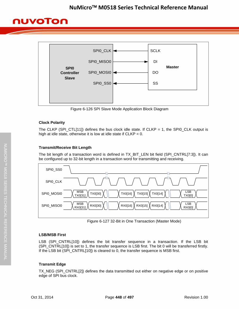
NuMicro M0518 Series Technical Reference Manual
Oct 31, 2014 Page 448 of 497 Revision 1.00
NU
MIC
RO
™ M
0518
SE
RIE
S T
EC
HN
ICA
L R
EF
ER
EN
CE
MA
NU
AL
SCLK
DI
DO
SS
Master
SPI0_CLK
SPI0_MISO0
SPI0_MOSI0
SPI0_SS0
SPI0
Controller
Slave
Figure 6-126 SPI Slave Mode Application Block Diagram
Clock Polarity
The CLKP (SPI_CTL[11]) defines the bus clock idle state. If CLKP = 1, the SPI0_CLK output is high at idle state, otherwise it is low at idle state if CLKP = 0.
Transmit/Receive Bit Length
The bit length of a transaction word is defined in TX_BIT_LEN bit field (SPI_CNTRL[7:3]). It can be configured up to 32-bit length in a transaction word for transmitting and receiving.
SPI0_CLK
SPI0_MISO0
SPI0_MOSI0 TX0[30] TX0[16] TX0[15] TX0[14]LSB
TX0[0]
RX0[30] RX0[16] RX0[14]LSB
RX0[0]
MSB
RX0[31]RX0[15]
MSB
TX0[31]
SPI0_SS0
Figure 6-127 32-Bit in One Transaction (Master Mode)
LSB/MSB First
LSB (SPI_CNTRL[10]) defines the bit transfer sequence in a transaction. If the LSB bit (SPI_CNTRL[10]) is set to 1, the transfer sequence is LSB first. The bit 0 will be transferred firstly. If the LSB bit (SPI_CNTRL[10]) is cleared to 0, the transfer sequence is MSB first.
Transmit Edge
TX_NEG (SPI_CNTRL[2]) defines the data transmitted out either on negative edge or on positive edge of SPI bus clock.
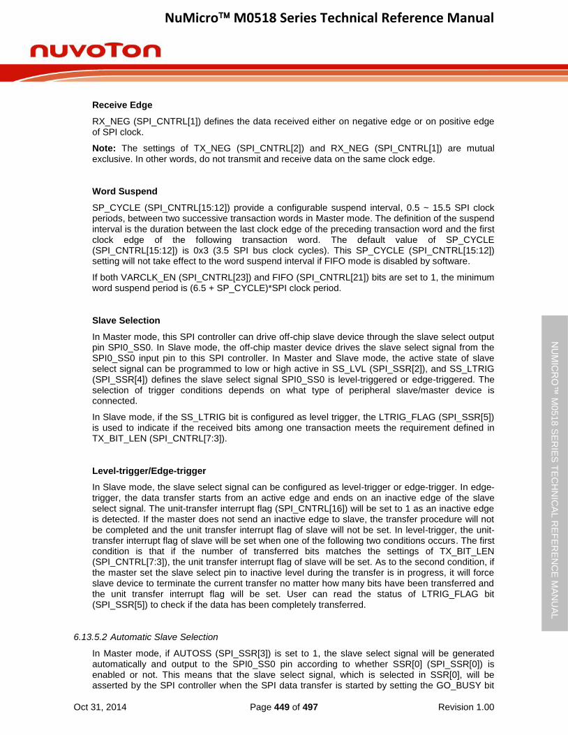
NuMicro M0518 Series Technical Reference Manual
Oct 31, 2014 Page 449 of 497 Revision 1.00
NU
MIC
RO
™ M
0518
SE
RIE
S T
EC
HN
ICA
L R
EF
ER
EN
CE
MA
NU
AL
Receive Edge
RX_NEG (SPI_CNTRL[1]) defines the data received either on negative edge or on positive edge of SPI clock.
Note: The settings of TX_NEG (SPI_CNTRL[2]) and RX_NEG (SPI_CNTRL[1]) are mutual exclusive. In other words, do not transmit and receive data on the same clock edge.
Word Suspend
SP_CYCLE (SPI_CNTRL[15:12]) provide a configurable suspend interval, 0.5 ~ 15.5 SPI clock periods, between two successive transaction words in Master mode. The definition of the suspend interval is the duration between the last clock edge of the preceding transaction word and the first clock edge of the following transaction word. The default value of SP_CYCLE (SPI_CNTRL[15:12]) is 0x3 (3.5 SPI bus clock cycles). This SP_CYCLE (SPI_CNTRL[15:12]) setting will not take effect to the word suspend interval if FIFO mode is disabled by software.
If both VARCLK_EN (SPI_CNTRL[23]) and FIFO (SPI_CNTRL[21]) bits are set to 1, the minimum word suspend period is (6.5 + SP_CYCLE)*SPI clock period.
Slave Selection
In Master mode, this SPI controller can drive off-chip slave device through the slave select output pin SPI0_SS0. In Slave mode, the off-chip master device drives the slave select signal from the SPI0_SS0 input pin to this SPI controller. In Master and Slave mode, the active state of slave select signal can be programmed to low or high active in SS_LVL (SPI_SSR[2]), and SS_LTRIG (SPI_SSR[4]) defines the slave select signal SPI0_SS0 is level-triggered or edge-triggered. The selection of trigger conditions depends on what type of peripheral slave/master device is connected.
In Slave mode, if the SS_LTRIG bit is configured as level trigger, the LTRIG_FLAG (SPI_SSR[5]) is used to indicate if the received bits among one transaction meets the requirement defined in TX_BIT_LEN (SPI_CNTRL[7:3]).
Level-trigger/Edge-trigger
In Slave mode, the slave select signal can be configured as level-trigger or edge-trigger. In edge-trigger, the data transfer starts from an active edge and ends on an inactive edge of the slave select signal. The unit-transfer interrupt flag (SPI_CNTRL[16]) will be set to 1 as an inactive edge is detected. If the master does not send an inactive edge to slave, the transfer procedure will not be completed and the unit transfer interrupt flag of slave will not be set. In level-trigger, the unit-transfer interrupt flag of slave will be set when one of the following two conditions occurs. The first condition is that if the number of transferred bits matches the settings of TX_BIT_LEN (SPI_CNTRL[7:3]), the unit transfer interrupt flag of slave will be set. As to the second condition, if the master set the slave select pin to inactive level during the transfer is in progress, it will force slave device to terminate the current transfer no matter how many bits have been transferred and the unit transfer interrupt flag will be set. User can read the status of LTRIG_FLAG bit (SPI_SSR[5]) to check if the data has been completely transferred.
6.13.5.2 Automatic Slave Selection
In Master mode, if AUTOSS (SPI_SSR[3]) is set to 1, the slave select signal will be generated automatically and output to the SPI0_SS0 pin according to whether SSR[0] (SPI_SSR[0]) is enabled or not. This means that the slave select signal, which is selected in SSR[0], will be asserted by the SPI controller when the SPI data transfer is started by setting the GO_BUSY bit
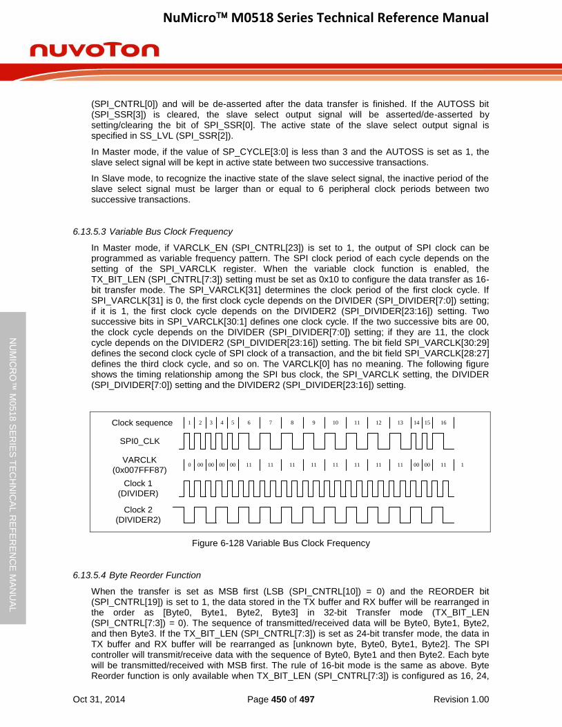
NuMicro M0518 Series Technical Reference Manual
Oct 31, 2014 Page 450 of 497 Revision 1.00
NU
MIC
RO
™ M
0518
SE
RIE
S T
EC
HN
ICA
L R
EF
ER
EN
CE
MA
NU
AL
(SPI_CNTRL[0]) and will be de-asserted after the data transfer is finished. If the AUTOSS bit (SPI_SSR[3]) is cleared, the slave select output signal will be asserted/de-asserted by setting/clearing the bit of SPI_SSR[0]. The active state of the slave select output signal is specified in SS_LVL (SPI_SSR[2]).
In Master mode, if the value of SP_CYCLE[3:0] is less than 3 and the AUTOSS is set as 1, the slave select signal will be kept in active state between two successive transactions.
In Slave mode, to recognize the inactive state of the slave select signal, the inactive period of the slave select signal must be larger than or equal to 6 peripheral clock periods between two successive transactions.
6.13.5.3 Variable Bus Clock Frequency
In Master mode, if VARCLK_EN (SPI_CNTRL[23]) is set to 1, the output of SPI clock can be programmed as variable frequency pattern. The SPI clock period of each cycle depends on the setting of the SPI_VARCLK register. When the variable clock function is enabled, the TX_BIT_LEN (SPI_CNTRL[7:3]) setting must be set as 0x10 to configure the data transfer as 16-bit transfer mode. The SPI_VARCLK[31] determines the clock period of the first clock cycle. If SPI_VARCLK[31] is 0, the first clock cycle depends on the DIVIDER (SPI_DIVIDER[7:0]) setting; if it is 1, the first clock cycle depends on the DIVIDER2 (SPI_DIVIDER[23:16]) setting. Two successive bits in SPI_VARCLK[30:1] defines one clock cycle. If the two successive bits are 00, the clock cycle depends on the DIVIDER (SPI_DIVIDER[7:0]) setting; if they are 11, the clock cycle depends on the DIVIDER2 (SPI_DIVIDER[23:16]) setting. The bit field SPI_VARCLK[30:29] defines the second clock cycle of SPI clock of a transaction, and the bit field SPI_VARCLK[28:27] defines the third clock cycle, and so on. The VARCLK[0] has no meaning. The following figure shows the timing relationship among the SPI bus clock, the SPI_VARCLK setting, the DIVIDER (SPI_DIVIDER[7:0]) setting and the DIVIDER2 (SPI_DIVIDER[23:16]) setting.
SPI0_CLK
VARCLK
(0x007FFF87)
Clock 1
(DIVIDER)
Clock 2
(DIVIDER2)
Clock sequence 1 2 3 4 5 6 7 8 9 10 11 12 13 14 15 16
0 00 00 00 00 11 11 11 11 11 11 11 11 00 00 11 1
Figure 6-128 Variable Bus Clock Frequency
6.13.5.4 Byte Reorder Function
When the transfer is set as MSB first (LSB (SPI_CNTRL[10]) = 0) and the REORDER bit (SPI_CNTRL[19]) is set to 1, the data stored in the TX buffer and RX buffer will be rearranged in the order as [Byte0, Byte1, Byte2, Byte3] in 32-bit Transfer mode (TX_BIT_LEN (SPI_CNTRL[7:3]) = 0). The sequence of transmitted/received data will be Byte0, Byte1, Byte2, and then Byte3. If the TX_BIT_LEN (SPI_CNTRL[7:3]) is set as 24-bit transfer mode, the data in TX buffer and RX buffer will be rearranged as [unknown byte, Byte0, Byte1, Byte2]. The SPI controller will transmit/receive data with the sequence of Byte0, Byte1 and then Byte2. Each byte will be transmitted/received with MSB first. The rule of 16-bit mode is the same as above. Byte Reorder function is only available when TX_BIT_LEN (SPI_CNTRL[7:3]) is configured as 16, 24,
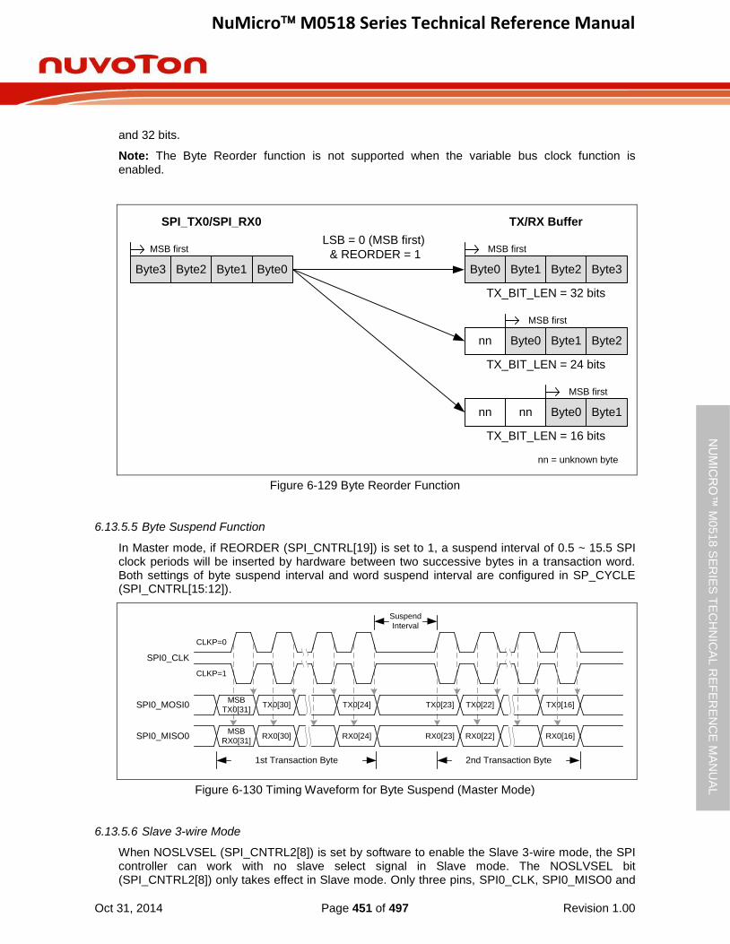
NuMicro M0518 Series Technical Reference Manual
Oct 31, 2014 Page 451 of 497 Revision 1.00
NU
MIC
RO
™ M
0518
SE
RIE
S T
EC
HN
ICA
L R
EF
ER
EN
CE
MA
NU
AL
and 32 bits.
Note: The Byte Reorder function is not supported when the variable bus clock function is enabled.
Byte3 Byte0Byte1Byte2
SPI_TX0/SPI_RX0 TX/RX Buffer
LSB = 0 (MSB first)
& REORDER = 1
TX_BIT_LEN = 24 bits
TX_BIT_LEN = 16 bits
TX_BIT_LEN = 32 bits
MSB first
MSB first
nn = unknown byte
nn Byte1Byte0nn
Byte1Byte0nn Byte2
MSB first
Byte3Byte0 Byte1 Byte2
MSB first
Figure 6-129 Byte Reorder Function
6.13.5.5 Byte Suspend Function
In Master mode, if REORDER (SPI_CNTRL[19]) is set to 1, a suspend interval of 0.5 ~ 15.5 SPI clock periods will be inserted by hardware between two successive bytes in a transaction word. Both settings of byte suspend interval and word suspend interval are configured in SP_CYCLE (SPI_CNTRL[15:12]).
SPI0_CLK
SPI0_MISO0
SPI0_MOSI0 TX0[30] TX0[24] TX0[23] TX0[22] TX0[16]
RX0[30] RX0[24] RX0[22] RX0[16]MSB
RX0[31]
CLKP=0
CLKP=1
Suspend
Interval
1st Transaction Byte 2nd Transaction Byte
RX0[23]
MSB
TX0[31]
Figure 6-130 Timing Waveform for Byte Suspend (Master Mode)
6.13.5.6 Slave 3-wire Mode
When NOSLVSEL (SPI_CNTRL2[8]) is set by software to enable the Slave 3-wire mode, the SPI controller can work with no slave select signal in Slave mode. The NOSLVSEL bit (SPI_CNTRL2[8]) only takes effect in Slave mode. Only three pins, SPI0_CLK, SPI0_MISO0 and
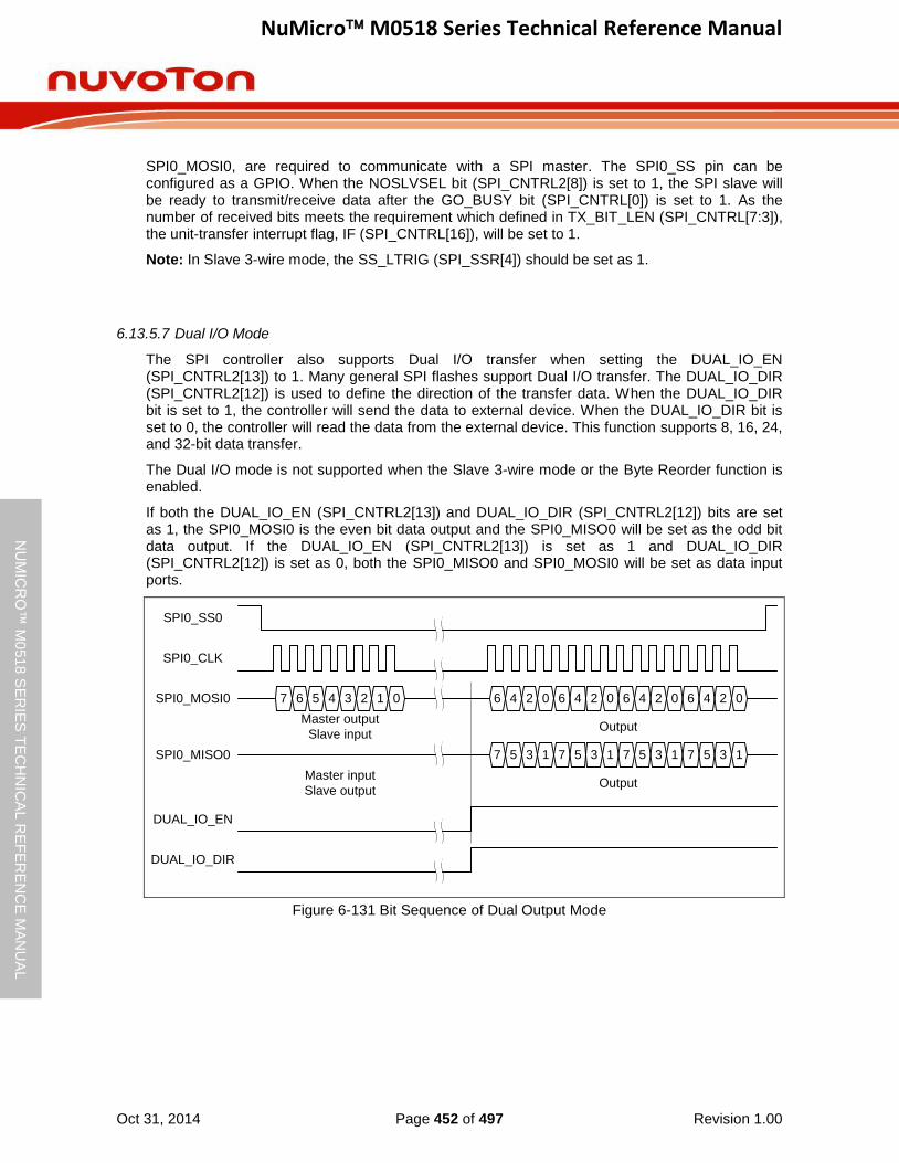
NuMicro M0518 Series Technical Reference Manual
Oct 31, 2014 Page 452 of 497 Revision 1.00
NU
MIC
RO
™ M
0518
SE
RIE
S T
EC
HN
ICA
L R
EF
ER
EN
CE
MA
NU
AL
SPI0_MOSI0, are required to communicate with a SPI master. The SPI0_SS pin can be configured as a GPIO. When the NOSLVSEL bit (SPI_CNTRL2[8]) is set to 1, the SPI slave will be ready to transmit/receive data after the GO_BUSY bit (SPI_CNTRL[0]) is set to 1. As the number of received bits meets the requirement which defined in TX_BIT_LEN (SPI_CNTRL[7:3]), the unit-transfer interrupt flag, IF (SPI_CNTRL[16]), will be set to 1.
Note: In Slave 3-wire mode, the SS_LTRIG (SPI_SSR[4]) should be set as 1.
6.13.5.7 Dual I/O Mode
The SPI controller also supports Dual I/O transfer when setting the DUAL_IO_EN (SPI_CNTRL2[13]) to 1. Many general SPI flashes support Dual I/O transfer. The DUAL_IO_DIR (SPI_CNTRL2[12]) is used to define the direction of the transfer data. When the DUAL_IO_DIR bit is set to 1, the controller will send the data to external device. When the DUAL_IO_DIR bit is set to 0, the controller will read the data from the external device. This function supports 8, 16, 24, and 32-bit data transfer.
The Dual I/O mode is not supported when the Slave 3-wire mode or the Byte Reorder function is enabled.
If both the DUAL_IO_EN (SPI_CNTRL2[13]) and DUAL_IO_DIR (SPI_CNTRL2[12]) bits are set as 1, the SPI0_MOSI0 is the even bit data output and the SPI0_MISO0 will be set as the odd bit data output. If the DUAL_IO_EN (SPI_CNTRL2[13]) is set as 1 and DUAL_IO_DIR (SPI_CNTRL2[12]) is set as 0, both the SPI0_MISO0 and SPI0_MOSI0 will be set as data input ports.
SPI0_SS0
7 6 5 4 3 2 1 0
SPI0_CLK
SPI0_MOSI0
SPI0_MISO0
DUAL_IO_EN
6 4 2 0 6 4 2 0
7 5 3 1 7 5 3 1
6 4 2 0 6 4 2 0
7 5 3 1 7 5 3 1
DUAL_IO_DIR
Master output
Slave input
Master input
Slave output
Output
Output
Figure 6-131 Bit Sequence of Dual Output Mode
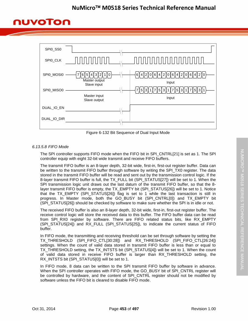
NuMicro M0518 Series Technical Reference Manual
Oct 31, 2014 Page 453 of 497 Revision 1.00
NU
MIC
RO
™ M
0518
SE
RIE
S T
EC
HN
ICA
L R
EF
ER
EN
CE
MA
NU
AL
SPI0_SS0
7 6 5 4 3 2 1 0
SPI0_CLK
SPI0_MOSI0
SPI0_MISO0
DUAL_IO_EN
6 4 2 0 6 4 2 0
7 5 3 1 7 5 3 1
6 4 2 0 6 4 2 0
7 5 3 1 7 5 3 1
DUAL_IO_DIR
Master output
Slave input
Master input
Slave outputInput
Input
Figure 6-132 Bit Sequence of Dual Input Mode
6.13.5.8 FIFO Mode
The SPI controller supports FIFO mode when the FIFO bit in SPI_CNTRL[21] is set as 1. The SPI controller equip with eight 32-bit wide transmit and receive FIFO buffers.
The transmit FIFO buffer is an 8-layer depth, 32-bit wide, first-in, first-out register buffer. Data can be written to the transmit FIFO buffer through software by writing the SPI_TX0 register. The data stored in the transmit FIFO buffer will be read and sent out by the transmission control logic. If the 8-layer transmit FIFO buffer is full, the TX_FULL bit (SPI_STATUS[27]) will be set to 1. When the SPI transmission logic unit draws out the last datum of the transmit FIFO buffer, so that the 8-layer transmit FIFO buffer is empty, the TX_EMPTY bit (SPI_STATUS[26]) will be set to 1. Notice that the TX_EMPTY (SPI_STATUS[26]) flag is set to 1 while the last transaction is still in progress. In Master mode, both the GO_BUSY bit (SPI_CNTRL[0]) and TX_EMPTY bit (SPI_STATUS[26]) should be checked by software to make sure whether the SPI is in idle or not.
The received FIFO buffer is also an 8-layer depth, 32-bit wide, first-in, first-out register buffer. The receive control logic will store the received data to this buffer. The FIFO buffer data can be read from SPI_RX0 register by software. There are FIFO related status bits, like RX_EMPTY (SPI_STATUS[24]) and RX_FULL (SPI_STATUS[25]), to indicate the current status of FIFO buffer.
In FIFO mode, the transmitting and receiving threshold can be set through software by setting the TX_THRESHOLD (SPI_FIFO_CTL[30:28]) and RX_THRESHOLD (SPI_FIFO_CTL[26:24]) settings. When the count of valid data stored in transmit FIFO buffer is less than or equal to TX_THRESHOLD setting, the TX_INTSTS bit (SPI_STATUS[4]) will be set to 1. When the count of valid data stored in receive FIFO buffer is larger than RX_THRESHOLD setting, the RX_INTSTS bit (SPI_STATUS[0]) will be set to 1.
In FIFO mode, 8 data can be written to the SPI transmit FIFO buffer by software in advance. When the SPI controller operates with FIFO mode, the GO_BUSY bit of SPI_CNTRL register will be controlled by hardware, and the content of SPI_CNTRL register should not be modified by software unless the FIFO bit is cleared to disable FIFO mode.

NuMicro M0518 Series Technical Reference Manual
Oct 31, 2014 Page 454 of 497 Revision 1.00
NU
MIC
RO
™ M
0518
SE
RIE
S T
EC
HN
ICA
L R
EF
ER
EN
CE
MA
NU
AL
Receive buffer nReceive buffer 2
Transmit buffer nTransmit buffer 2
Receive buffer 1
Transmit buffer 1
SPI0_MOSI0 Pin in Master Mode
or
SPI0_MISO0 Pin in Slave Mode
SPI0_MISO0 Pin in Master Mode
or
SPI0_MOSI0 Pin in Slave Mode
SPI_TX Buffer
Transmit Buffer 0
Receive Buffer 0
SPI_RX Buffer
APB
Write
Read
12
n
12
n
Figure 6-133 FIFO Mode Block Diagram
In Master mode, when the FIFO bit is set to 1 and the first datum is written to the SPI_TX0 register, the TX_EMPTY (SPI_STATUS[26]) flag will be cleared to 0. The transmission immediately starts as long as the transmit FIFO buffer is not empty. User can write the next data into SPI_TX0 register immediately. The SPI controller will insert a suspend interval between two successive transactions in FIFO mode and the period of suspend interval is decided by the setting of SP_CYCLE (SPI_CNTRL[15:12]). User can write data into SPI_TX0 register as long as the TX_FULL (SPI_STATUS[27]) flag is 0.
The subsequent transactions will be triggered automatically if the transmitted data are updated in time. If the SPI_TX0 register does not be updated after all data transfer are done, the transfer will stop.
In Master mode, during receiving operation, the serial data are received from SPI0_MISO0 pin and stored to receive FIFO buffer. The RX_EMPTY (SPI_STATUS[24]) flag will be cleared to 0 while the receive FIFO buffer contains unread data. The received data can be read by software from SPI_RX0 register as long as the RX_EMPTY (SPI_STATUS[24]) flag is 0. If the receive FIFO buffer contains 8 unread data, the RX_FULL (SPI_STATUS[25]) flag will be set to 1. The SPI controller will stop receiving data until the SPI_RX0 register is read by software.
In Slave mode, when the FIFO bit is set as 1, the GO_BUSY bit will be set as 1 by hardware automatically.
In Slave mode, during transmission operation, when data is written to the SPI_TX0 register by software, the data will be loaded into transmit FIFO buffer and the TX_EMPTY (SPI_STATUS[26]) flag will be set to 0. The transmission will start when the slave device receives clock signal from master. Data can be written to SPI_TX0 register as long as the TX_FULL (SPI_STATUS[27]) flag is 0. After all data have been drawn out by the SPI transmission logic unit and the SPI_TX0 register is not updated by software, the TX_EMPTY (SPI_STATUS[26]) flag will be set to 1.
In Slave mode, during receiving operation, the serial data is received from SPI0_MOSI0 pin and stored to receive FIFO buffer. The reception mechanism is similar to Master mode reception operation.
NuMicro M0518 Series Technical Reference Manual
Oct 31, 2014 Page 455 of 497 Revision 1.00
NU
MIC
RO
™ M
0518
SE
RIE
S T
EC
HN
ICA
L R
EF
ER
EN
CE
MA
NU
AL
6.13.5.9 Interrupt
SPI unit transfer interrupt
As the SPI controller finishes a unit transfer, the unit transfer interrupt flag IF (SPI_CNTRL[16]) will be set to 1. The unit transfer interrupt event will generate an interrupt to CPU if the unit transfer interrupt enable bit IE (SPI_CNTRL[17]) is set. The unit transfer interrupt flag can be cleared only by writing 1 to it.
SPI Slave 3-wire mode start interrupt
In 3-wire mode, the slave 3-wire mode start interrupt flag, SLV_START_INTSTS (SPI_CNTRL2[11]), will be set to 1 when the slave senses the SPI clock signal. The SPI controller will issue an interrupt if the SSTA_INTEN (SPI_CNTRL2[10]) is set to 1. If the count of the received bits is less than the setting of TX_BIT_LEN and there is no more SPI clock input over the expected time period which is defined by the user, the user can set the SLV_ABORT bit (SPI_CNTRL2[9]) to abort the current transfer. The unit transfer interrupt flag, IF, will be set to 1 if the software set the SLV_ABORT bit (SPI_CNTRL2[9]).
Receive FIFO time-out interrupt
In FIFO mode, there is a time-out function to inform user. If there is a received data in the FIFO and it is not read by software over 64 SPI peripheral clock periods in Master mode or over 576 SPI peripheral clock periods in Slave mode, it will send a time-out interrupt to the system if the time-out interrupt enable bit, SPI_FIFO_CTL[21], is set to 1.
Transmit FIFO interrupt
In FIFO mode, if the valid data count of the transmit FIFO buffer is less than or equal to the setting value of TX_THRESHOLD, the transmit FIFO interrupt flag will be set to 1. The SPI controller will generate a transmit FIFO interrupt to the system if the transmit FIFO interrupt enable bit, SPI_FIFO_CTL[3], is set to 1.
Receive FIFO interrupt
In FIFO mode, if the valid data count of the receive FIFO buffer is larger than the setting value of RX_THRESHOLD, the receive FIFO interrupt flag will be set to 1. The SPI controller will generate a receive FIFO interrupt to the system if the receive FIFO interrupt enable bit, SPI_FIFO_CTL[2], is set to 1.
6.13.6 Timing Diagram
The active state of slave select signal can be defined by setting the SS_LVL (SPI_SSR[2]) and SS_LTRIG (SPI_SSR[4]). The SPI clock which is in idle state can be configured as high or low state by setting the CLKP (SPI_CNTRL[11]). It also provides the bit length of a transaction word in TX_BIT_LEN (SPI_CNTRL[7:3]), and transmitting/receiving data from MSB or LSB first in LSB (SPI_CNTRL[10]). User can also select which edge of SPI clock to transmit/receive data in TX_NEG/RX_NEG (SPI_CNTRL[2:1]). Four SPI timing diagrams for master/slave operations and the related settings are shown below.
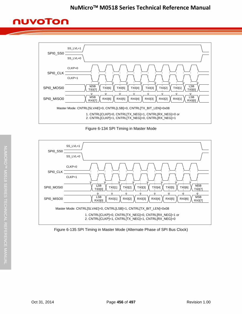
NuMicro M0518 Series Technical Reference Manual
Oct 31, 2014 Page 456 of 497 Revision 1.00
NU
MIC
RO
™ M
0518
SE
RIE
S T
EC
HN
ICA
L R
EF
ER
EN
CE
MA
NU
AL
SPI0_CLK
SPI0_MISO0
SPI0_MOSI0 TX0[6] TX0[4] TX0[3] TX0[2]LSB
TX0[0]
RX0[6] RX0[4] RX0[2]LSB
RX0[0]
MSB
RX0[7]RX0[3]
MSB
TX0[7]
SPI0_SS0
CLKP=0
CLKP=1
TX0[5]
RX0[5]
TX0[1]
RX0[1]
SS_LVL=0
SS_LVL=1
Master Mode: CNTRL[SLVAE]=0, CNTRL[LSB]=0, CNTRL[TX_BIT_LEN]=0x08
1. CNTRL[CLKP]=0, CNTRL[TX_NEG]=1, CNTRL[RX_NEG]=0 or
2. CNTRL[CLKP]=1, CNTRL[TX_NEG]=0, CNTRL[RX_NEG]=1
Figure 6-134 SPI Timing in Master Mode
SPI0_CLK
SPI0_MISO0
SPI0_MOSI0 TX0[1] TX0[3] TX0[4] TX0[5]MSB
TX0[7]
RX0[1] RX0[3] RX0[5]MSB
RX0[7]
LSB
RX0[0]RX0[4]
LSB
TX0[0]
SPI0_SS0
CLKP=0
CLKP=1
TX0[2]
RX0[2]
TX0[6]
RX0[6]
SS_LVL=0
SS_LVL=1
Master Mode: CNTRL[SLVAE]=0, CNTRL[LSB]=1, CNTRL[TX_BIT_LEN]=0x08
1. CNTRL[CLKP]=0, CNTRL[TX_NEG]=0, CNTRL[RX_NEG]=1 or
2. CNTRL[CLKP]=1, CNTRL[TX_NEG]=1, CNTRL[RX_NEG]=0
Figure 6-135 SPI Timing in Master Mode (Alternate Phase of SPI Bus Clock)
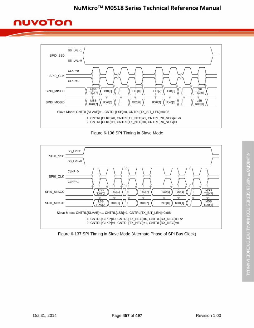
NuMicro M0518 Series Technical Reference Manual
Oct 31, 2014 Page 457 of 497 Revision 1.00
NU
MIC
RO
™ M
0518
SE
RIE
S T
EC
HN
ICA
L R
EF
ER
EN
CE
MA
NU
AL
SPI0_CLK
SPI0_MOSI0
SPI0_MISO0 TX0[6] TX0[0] TX0[7] TX0[6]LSB
TX0[0]
RX0[6] RX0[0] RX0[6]LSB
RX0[0]
MSB
RX0[7]RX0[7]
MSB
TX0[7]
SPI0_SS0
CLKP=0
CLKP=1
SS_LVL=0
SS_LVL=1
Slave Mode: CNTRL[SLVAE]=1, CNTRL[LSB]=0, CNTRL[TX_BIT_LEN]=0x08
1. CNTRL[CLKP]=0, CNTRL[TX_NEG]=1, CNTRL[RX_NEG]=0 or
2. CNTRL[CLKP]=1, CNTRL[TX_NEG]=0, CNTRL[RX_NEG]=1
Figure 6-136 SPI Timing in Slave Mode
SPI0_CLK
SPI0_MOSI0
SPI0_MISO0 TX0[1] TX0[7] TX0[0] TX0[1]MSB
TX0[7]
RX0[1] RX0[7] RX0[1]MSB
RX0[7]
LSB
RX0[0]RX0[0]
LSB
TX0[0]
SPI0_SS0
CLKP=0
CLKP=1
SS_LVL=0
SS_LVL=1
Slave Mode: CNTRL[SLVAE]=1, CNTRL[LSB]=1, CNTRL[TX_BIT_LEN]=0x08
1. CNTRL[CLKP]=0, CNTRL[TX_NEG]=0, CNTRL[RX_NEG]=1 or
2. CNTRL[CLKP]=1, CNTRL[TX_NEG]=1, CNTRL[RX_NEG]=0
Figure 6-137 SPI Timing in Slave Mode (Alternate Phase of SPI Bus Clock)

NuMicro M0518 Series Technical Reference Manual
Oct 31, 2014 Page 458 of 497 Revision 1.00
NU
MIC
RO
™ M
0518
SE
RIE
S T
EC
HN
ICA
L R
EF
ER
EN
CE
MA
NU
AL
6.13.7 Programming Examples
Example 1: The SPI controller is set as a master to access an off-chip slave device with the following specifications:
Data bit is latched on positive edge of SPI clock.
Data bit is driven on negative edge of SPI clock.
Data is transferred from MSB first.
SPI bus clock is low at idle state.
Only one byte of data to be transmitted/received in a transaction.
Uses the first SPI slave select pin to connect with an off-chip slave device. The slave select signal is active low.
The operation flow is as follows.
1) Set the DIVIDER (SPI_DIVIDER [7:0]) register to determine the output frequency of SPI clock.
2) Write the SPI_SSR register a proper value for the related settings of Master mode:
1. Clear the Automatic Slave Selection bit, AUTOSS (SPI_SSR[3]), to 0.
2. Select low level trigger output of slave select signal in the Slave Select Active Level bit, SS_LVL (SPI_SSR[2]), and Slave Select Level Trigger bit, SS_LTRIG (SPI_SSR[4]).
3. Select slave select signal to be output active at the I/O pin by setting the Slave Select Register bit SSR[0] (SPI_SSR[0]) to active the off-chip slave device.
3) Write the related settings into the SPI_CNTRL register to control the SPI master actions
1. Set this SPI controller as master device in SLAVE bit (SPI_CNTRL[18] = 0).
2. Force the SPI clock to low at idle state in CLKP bit (SPI_CNTRL[11] = 0).
3. Select data transmitted at negative edge of SPI clock in TX_NEG bit (SPI_CNTRL[2] = 1).
4. Select data latched at positive edge of SPI clock in RX_NEG bit (SPI_CNTRL[1] = 0).
5. Set the bit length of word transfer as 8-bit in TX_BIT_LEN bit field. (SPI_CNTRL[7:3] = 0x08).
6. Set MSB transfer first in MSB bit (SPI_CNTRL[10] = 0).
4) If this SPI master attempts to transmit (write) one byte data to the off-chip slave device, write the byte data that will be transmitted into the SPI_TX0 register.
5) If this SPI master just only attempts to receive (read) one byte data from the off-chip slave device and does not care what data will be transmitted, the SPI_TX0 register does not need to be updated by software.
6) Enable the GO_BUSY bit (SPI_CNTRL [0] = 1) to start the data transfer with the SPI interface.
7) Waiting for SPI interrupt (if the Interrupt Enable IE bit is set) or just polling the GO_BUSY bit till it is cleared to 0 by hardware automatically.
8) Read out the received one byte data from SPI_RX0[7:0].
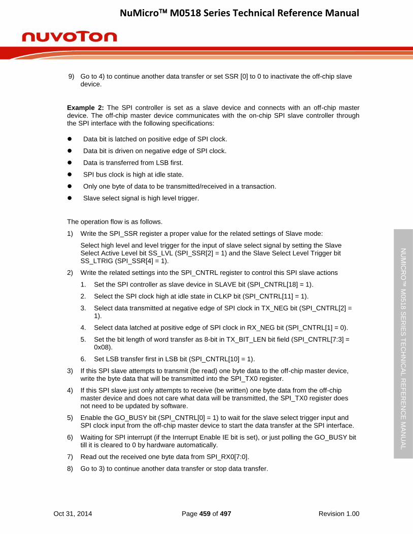
NuMicro M0518 Series Technical Reference Manual
Oct 31, 2014 Page 459 of 497 Revision 1.00
NU
MIC
RO
™ M
0518
SE
RIE
S T
EC
HN
ICA
L R
EF
ER
EN
CE
MA
NU
AL
9) Go to 4) to continue another data transfer or set SSR [0] to 0 to inactivate the off-chip slave device.
Example 2: The SPI controller is set as a slave device and connects with an off-chip master device. The off-chip master device communicates with the on-chip SPI slave controller through the SPI interface with the following specifications:
Data bit is latched on positive edge of SPI clock.
Data bit is driven on negative edge of SPI clock.
Data is transferred from LSB first.
SPI bus clock is high at idle state.
Only one byte of data to be transmitted/received in a transaction.
Slave select signal is high level trigger.
The operation flow is as follows.
1) Write the SPI_SSR register a proper value for the related settings of Slave mode:
Select high level and level trigger for the input of slave select signal by setting the Slave Select Active Level bit SS_LVL (SPI_SSR[2] = 1) and the Slave Select Level Trigger bit SS_LTRIG (SPI_SSR[4] = 1).
2) Write the related settings into the SPI_CNTRL register to control this SPI slave actions
1. Set the SPI controller as slave device in SLAVE bit (SPI_CNTRL[18] = 1).
2. Select the SPI clock high at idle state in CLKP bit (SPI_CNTRL[11] = 1).
3. Select data transmitted at negative edge of SPI clock in TX_NEG bit (SPI_CNTRL[2] = 1).
4. Select data latched at positive edge of SPI clock in RX_NEG bit (SPI_CNTRL[1] = 0).
5. Set the bit length of word transfer as 8-bit in TX_BIT_LEN bit field (SPI_CNTRL[7:3] = 0x08).
6. Set LSB transfer first in LSB bit (SPI_CNTRL[10] = 1).
3) If this SPI slave attempts to transmit (be read) one byte data to the off-chip master device, write the byte data that will be transmitted into the SPI_TX0 register.
4) If this SPI slave just only attempts to receive (be written) one byte data from the off-chip master device and does not care what data will be transmitted, the SPI_TX0 register does not need to be updated by software.
5) Enable the GO_BUSY bit (SPI_CNTRL[0] = 1) to wait for the slave select trigger input and SPI clock input from the off-chip master device to start the data transfer at the SPI interface.
6) Waiting for SPI interrupt (if the Interrupt Enable IE bit is set), or just polling the GO_BUSY bit till it is cleared to 0 by hardware automatically.
7) Read out the received one byte data from SPI_RX0[7:0].
8) Go to 3) to continue another data transfer or stop data transfer.
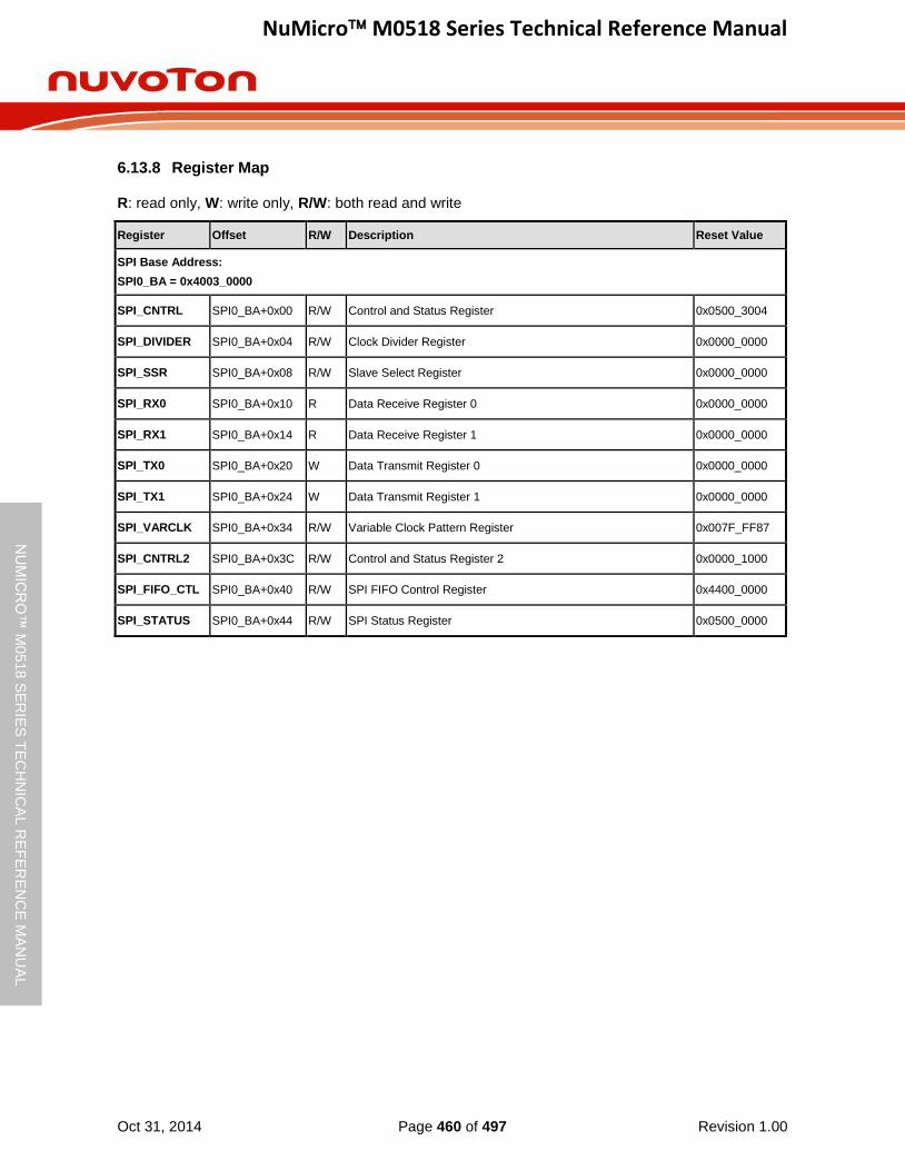
NuMicro M0518 Series Technical Reference Manual
Oct 31, 2014 Page 460 of 497 Revision 1.00
NU
MIC
RO
™ M
0518
SE
RIE
S T
EC
HN
ICA
L R
EF
ER
EN
CE
MA
NU
AL
6.13.8 Register Map
R: read only, W: write only, R/W: both read and write
Register Offset R/W Description Reset Value
SPI Base Address:
SPI0_BA = 0x4003_0000
SPI_CNTRL SPI0_BA+0x00 R/W Control and Status Register 0x0500_3004
SPI_DIVIDER SPI0_BA+0x04 R/W Clock Divider Register 0x0000_0000
SPI_SSR SPI0_BA+0x08 R/W Slave Select Register 0x0000_0000
SPI_RX0 SPI0_BA+0x10 R Data Receive Register 0 0x0000_0000
SPI_RX1 SPI0_BA+0x14 R Data Receive Register 1 0x0000_0000
SPI_TX0 SPI0_BA+0x20 W Data Transmit Register 0 0x0000_0000
SPI_TX1 SPI0_BA+0x24 W Data Transmit Register 1 0x0000_0000
SPI_VARCLK SPI0_BA+0x34 R/W Variable Clock Pattern Register 0x007F_FF87
SPI_CNTRL2 SPI0_BA+0x3C R/W Control and Status Register 2 0x0000_1000
SPI_FIFO_CTL SPI0_BA+0x40 R/W SPI FIFO Control Register 0x4400_0000
SPI_STATUS SPI0_BA+0x44 R/W SPI Status Register 0x0500_0000
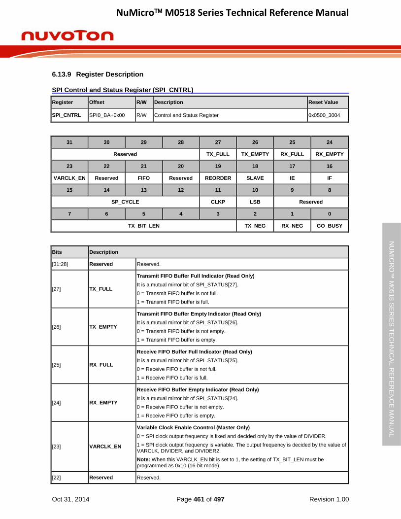
NuMicro M0518 Series Technical Reference Manual
Oct 31, 2014 Page 461 of 497 Revision 1.00
NU
MIC
RO
™ M
0518
SE
RIE
S T
EC
HN
ICA
L R
EF
ER
EN
CE
MA
NU
AL
6.13.9 Register Description
SPI Control and Status Register (SPI_CNTRL)
Register Offset R/W Description Reset Value
SPI_CNTRL SPI0_BA+0x00 R/W Control and Status Register 0x0500_3004
31 30 29 28 27 26 25 24
Reserved TX_FULL TX_EMPTY RX_FULL RX_EMPTY
23 22 21 20 19 18 17 16
VARCLK_EN Reserved FIFO Reserved REORDER SLAVE IE IF
15 14 13 12 11 10 9 8
SP_CYCLE CLKP LSB Reserved
7 6 5 4 3 2 1 0
TX_BIT_LEN TX_NEG RX_NEG GO_BUSY
Bits Description
[31:28] Reserved Reserved.
[27] TX_FULL
Transmit FIFO Buffer Full Indicator (Read Only)
It is a mutual mirror bit of SPI_STATUS[27].
0 = Transmit FIFO buffer is not full.
1 = Transmit FIFO buffer is full.
[26] TX_EMPTY
Transmit FIFO Buffer Empty Indicator (Read Only)
It is a mutual mirror bit of SPI_STATUS[26].
0 = Transmit FIFO buffer is not empty.
1 = Transmit FIFO buffer is empty.
[25] RX_FULL
Receive FIFO Buffer Full Indicator (Read Only)
It is a mutual mirror bit of SPI_STATUS[25].
0 = Receive FIFO buffer is not full.
1 = Receive FIFO buffer is full.
[24] RX_EMPTY
Receive FIFO Buffer Empty Indicator (Read Only)
It is a mutual mirror bit of SPI_STATUS[24].
0 = Receive FIFO buffer is not empty.
1 = Receive FIFO buffer is empty.
[23] VARCLK_EN
Variable Clock Enable Coontrol (Master Only)
0 = SPI clock output frequency is fixed and decided only by the value of DIVIDER.
1 = SPI clock output frequency is variable. The output frequency is decided by the value of VARCLK, DIVIDER, and DIVIDER2.
Note: When this VARCLK_EN bit is set to 1, the setting of TX_BIT_LEN must be programmed as 0x10 (16-bit mode).
[22] Reserved Reserved.
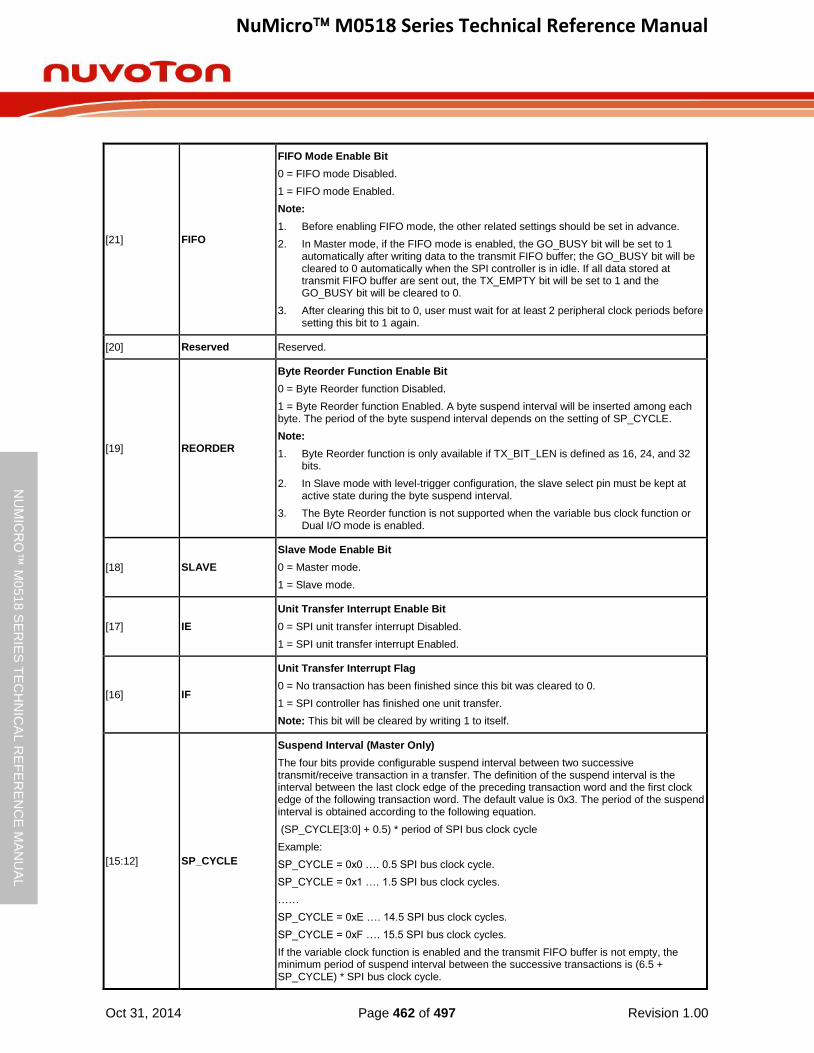
NuMicro M0518 Series Technical Reference Manual
Oct 31, 2014 Page 462 of 497 Revision 1.00
NU
MIC
RO
™ M
0518
SE
RIE
S T
EC
HN
ICA
L R
EF
ER
EN
CE
MA
NU
AL
[21] FIFO
FIFO Mode Enable Bit
0 = FIFO mode Disabled.
1 = FIFO mode Enabled.
Note:
1. Before enabling FIFO mode, the other related settings should be set in advance.
2. In Master mode, if the FIFO mode is enabled, the GO_BUSY bit will be set to 1 automatically after writing data to the transmit FIFO buffer; the GO_BUSY bit will be cleared to 0 automatically when the SPI controller is in idle. If all data stored at transmit FIFO buffer are sent out, the TX_EMPTY bit will be set to 1 and the GO_BUSY bit will be cleared to 0.
3. After clearing this bit to 0, user must wait for at least 2 peripheral clock periods before setting this bit to 1 again.
[20] Reserved Reserved.
[19] REORDER
Byte Reorder Function Enable Bit
0 = Byte Reorder function Disabled.
1 = Byte Reorder function Enabled. A byte suspend interval will be inserted among each byte. The period of the byte suspend interval depends on the setting of SP_CYCLE.
Note:
1. Byte Reorder function is only available if TX_BIT_LEN is defined as 16, 24, and 32 bits.
2. In Slave mode with level-trigger configuration, the slave select pin must be kept at active state during the byte suspend interval.
3. The Byte Reorder function is not supported when the variable bus clock function or Dual I/O mode is enabled.
[18] SLAVE
Slave Mode Enable Bit
0 = Master mode.
1 = Slave mode.
[17] IE
Unit Transfer Interrupt Enable Bit
0 = SPI unit transfer interrupt Disabled.
1 = SPI unit transfer interrupt Enabled.
[16] IF
Unit Transfer Interrupt Flag
0 = No transaction has been finished since this bit was cleared to 0.
1 = SPI controller has finished one unit transfer.
Note: This bit will be cleared by writing 1 to itself.
[15:12] SP_CYCLE
Suspend Interval (Master Only)
The four bits provide configurable suspend interval between two successive transmit/receive transaction in a transfer. The definition of the suspend interval is the interval between the last clock edge of the preceding transaction word and the first clock edge of the following transaction word. The default value is 0x3. The period of the suspend interval is obtained according to the following equation.
(SP_CYCLE[3:0] + 0.5) * period of SPI bus clock cycle
Example:
SP_CYCLE = 0x0 …. 0.5 SPI bus clock cycle.
SP_CYCLE = 0x1 …. 1.5 SPI bus clock cycles.
……
SP_CYCLE = 0xE …. 14.5 SPI bus clock cycles.
SP_CYCLE = 0xF …. 15.5 SPI bus clock cycles.
If the variable clock function is enabled and the transmit FIFO buffer is not empty, the minimum period of suspend interval between the successive transactions is (6.5 + SP_CYCLE) * SPI bus clock cycle.
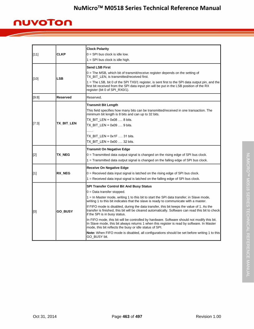
NuMicro M0518 Series Technical Reference Manual
Oct 31, 2014 Page 463 of 497 Revision 1.00
NU
MIC
RO
™ M
0518
SE
RIE
S T
EC
HN
ICA
L R
EF
ER
EN
CE
MA
NU
AL
[11] CLKP
Clock Polarity
0 = SPI bus clock is idle low.
1 = SPI bus clock is idle high.
[10] LSB
Send LSB First
0 = The MSB, which bit of transmit/receive register depends on the setting of TX_BIT_LEN, is transmitted/received first.
1 = The LSB, bit 0 of the SPI TX0/1 register, is sent first to the SPI data output pin, and the first bit received from the SPI data input pin will be put in the LSB position of the RX register (bit 0 of SPI_RX0/1).
[9:8] Reserved Reserved.
[7:3] TX_BIT_LEN
Transmit Bit Length
This field specifies how many bits can be transmitted/received in one transaction. The minimum bit length is 8 bits and can up to 32 bits.
TX_BIT_LEN = 0x08 …. 8 bits.
TX_BIT_LEN = 0x09 …. 9 bits.
……
TX_BIT_LEN = 0x1F …. 31 bits.
TX_BIT_LEN = 0x00 …. 32 bits.
[2] TX_NEG
Transmit On Negative Edge
0 = Transmitted data output signal is changed on the rising edge of SPI bus clock.
1 = Transmitted data output signal is changed on the falling edge of SPI bus clock.
[1] RX_NEG
Receive On Negative Edge
0 = Received data input signal is latched on the rising edge of SPI bus clock.
1 = Received data input signal is latched on the falling edge of SPI bus clock.
[0] GO_BUSY
SPI Transfer Control Bit And Busy Status
0 = Data transfer stopped.
1 = In Master mode, writing 1 to this bit to start the SPI data transfer; in Slave mode, writing 1 to this bit indicates that the slave is ready to communicate with a master.
If FIFO mode is disabled, during the data transfer, this bit keeps the value of 1. As the transfer is finished, this bit will be cleared automatically. Software can read this bit to check if the SPI is in busy status.
In FIFO mode, this bit will be controlled by hardware. Software should not modify this bit. In Slave mode, this bit always returns 1 when this register is read by software. In Master mode, this bit reflects the busy or idle status of SPI.
Note: When FIFO mode is disabled, all configurations should be set before writing 1 to this GO_BUSY bit.
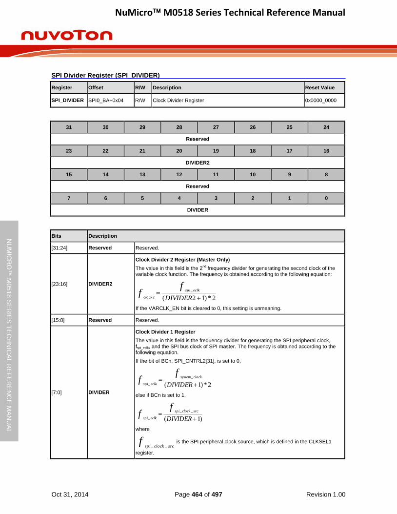
NuMicro M0518 Series Technical Reference Manual
Oct 31, 2014 Page 464 of 497 Revision 1.00
NU
MIC
RO
™ M
0518
SE
RIE
S T
EC
HN
ICA
L R
EF
ER
EN
CE
MA
NU
AL
SPI Divider Register (SPI_DIVIDER)
Register Offset R/W Description Reset Value
SPI_DIVIDER SPI0_BA+0x04 R/W Clock Divider Register 0x0000_0000
31 30 29 28 27 26 25 24
Reserved
23 22 21 20 19 18 17 16
DIVIDER2
15 14 13 12 11 10 9 8
Reserved
7 6 5 4 3 2 1 0
DIVIDER
Bits Description
[31:24] Reserved Reserved.
[23:16] DIVIDER2
Clock Divider 2 Register (Master Only)
The value in this field is the 2nd
frequency divider for generating the second clock of the variable clock function. The frequency is obtained according to the following equation:
2*)12(
_
2
DIVIDER
ff eclkspi
clock
If the VARCLK_EN bit is cleared to 0, this setting is unmeaning.
[15:8] Reserved Reserved.
[7:0] DIVIDER
Clock Divider 1 Register
The value in this field is the frequency divider for generating the SPI peripheral clock, fspi_eclk, and the SPI bus clock of SPI master. The frequency is obtained according to the following equation.
If the bit of BCn, SPI_CNTRL2[31], is set to 0,
2*)1(
_
_
DIVIDER
ff clocksystem
eclkspi
else if BCn is set to 1,
)1(
__
_
DIVIDER
ff srcclockspi
eclkspi
where
fsrcclockspi __
is the SPI peripheral clock source, which is defined in the CLKSEL1
register.

NuMicro M0518 Series Technical Reference Manual
Oct 31, 2014 Page 465 of 497 Revision 1.00
NU
MIC
RO
™ M
0518
SE
RIE
S T
EC
HN
ICA
L R
EF
ER
EN
CE
MA
NU
AL
SPI Slave Select Register (SPI_SSR)
Register Offset R/W Description Reset Value
SPI_SSR SPI0_BA+0x08 R/W Slave Select Register 0x0000_0000
31 30 29 28 27 26 25 24
Reserved
23 22 21 20 19 18 17 16
Reserved
15 14 13 12 11 10 9 8
Reserved
7 6 5 4 3 2 1 0
Reserved LTRIG_FLAG SS_LTRIG AUTOSS SS_LVL Reserved SSR
Bits Description
[31:6] Reserved Reserved.
[5] LTRIG_FLAG
Level Trigger Accomplish Flag
In Slave mode, this bit indicates whether the received bit number meets the requirement or not after the current transaction done.
0 = Transferred bit length of one transaction does not meet the specified requirement.
1 = Transferred bit length meets the specified requirement which defined in TX_BIT_LEN.
Note: This bit is READ only. As the GO_BUSY bit is set to 1 by software, the LTRIG_FLAG will be cleared to 0 after 4 SPI peripheral clock periods plus 1 system clock period. In FIFO mode, this bit has no meaning.
[4] SS_LTRIG
Slave Select Level Trigger Enable Bit (Slave Only)
0 = Slave select signal is edge-trigger. This is the default value. The SS_LVL bit decides the signal is active after a falling-edge or rising-edge.
1 = Slave select signal is level-trigger. The SS_LVL bit decides the signal is active low or active high.
[3] AUTOSS
Automatic Slave Select Function Enable Bit (Master Only)
0 = If this bit is cleared, slave select signal will be asserted/de-asserted by setting /clearing the corresponding bit of SPI_SSR[0].
1 = If this bit is set, SPI0_SPISS0 signal will be generated automatically. It means that device/slave select signal, which is set in SPI_SSR[0], will be asserted by the SPI controller when transmit/receive is started, and will be de-asserted after each transmit/receive is finished.
[2] SS_LVL
Slave Select Active Level
This bit defines the active status of slave select signal (SPI0_SPISS0).
0 = The slave select signal SPI0_SPISS0 is active on low-level/falling-edge.
1 = The slave select signal SPI0_SPISS0 is active on high-level/rising-edge.
[1] Reserved Reserved.
[0] SSR Slave Select Control Bit (Master Only)
If AUTOSS bit is cleared, writing 1 to any bit of this field sets the proper SPI0_SPISS0 line
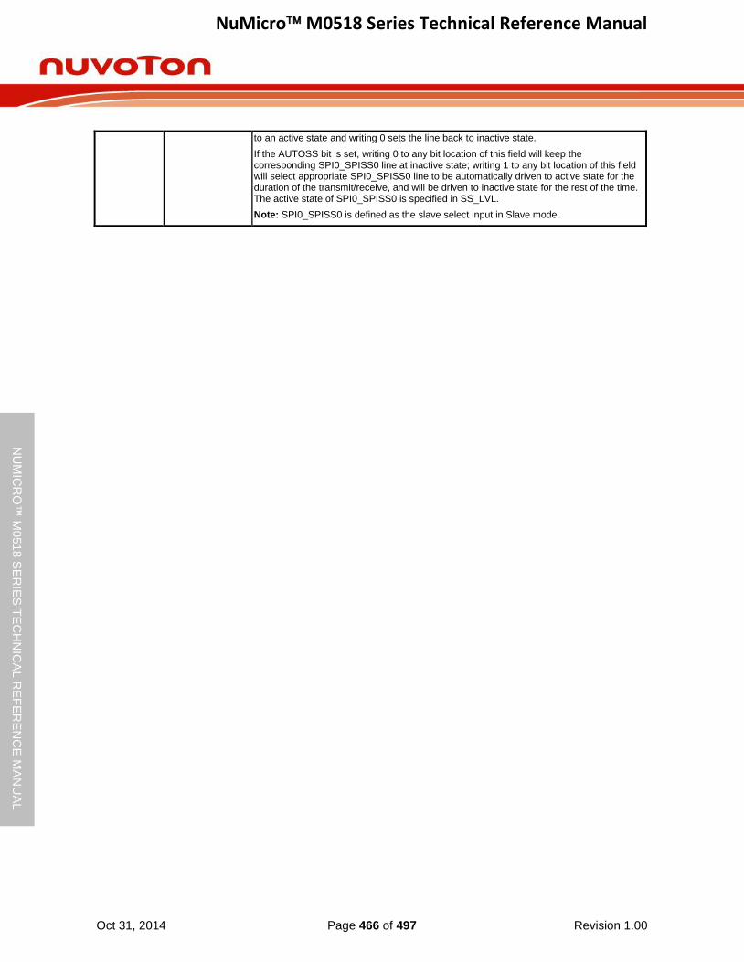
NuMicro M0518 Series Technical Reference Manual
Oct 31, 2014 Page 466 of 497 Revision 1.00
NU
MIC
RO
™ M
0518
SE
RIE
S T
EC
HN
ICA
L R
EF
ER
EN
CE
MA
NU
AL
to an active state and writing 0 sets the line back to inactive state.
If the AUTOSS bit is set, writing 0 to any bit location of this field will keep the corresponding SPI0_SPISS0 line at inactive state; writing 1 to any bit location of this field will select appropriate SPI0_SPISS0 line to be automatically driven to active state for the duration of the transmit/receive, and will be driven to inactive state for the rest of the time. The active state of SPI0_SPISS0 is specified in SS_LVL.
Note: SPI0_SPISS0 is defined as the slave select input in Slave mode.
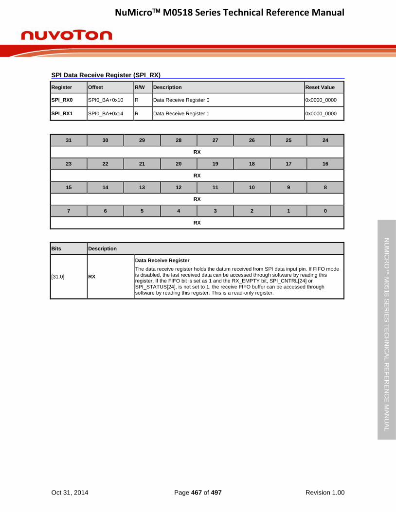
NuMicro M0518 Series Technical Reference Manual
Oct 31, 2014 Page 467 of 497 Revision 1.00
NU
MIC
RO
™ M
0518
SE
RIE
S T
EC
HN
ICA
L R
EF
ER
EN
CE
MA
NU
AL
SPI Data Receive Register (SPI_RX)
Register Offset R/W Description Reset Value
SPI_RX0 SPI0_BA+0x10 R Data Receive Register 0 0x0000_0000
SPI_RX1 SPI0_BA+0x14 R Data Receive Register 1 0x0000_0000
31 30 29 28 27 26 25 24
RX
23 22 21 20 19 18 17 16
RX
15 14 13 12 11 10 9 8
RX
7 6 5 4 3 2 1 0
RX
Bits Description
[31:0] RX
Data Receive Register
The data receive register holds the datum received from SPI data input pin. If FIFO mode is disabled, the last received data can be accessed through software by reading this register. If the FIFO bit is set as 1 and the RX_EMPTY bit, SPI_CNTRL[24] or SPI_STATUS[24], is not set to 1, the receive FIFO buffer can be accessed through software by reading this register. This is a read-only register.

NuMicro M0518 Series Technical Reference Manual
Oct 31, 2014 Page 468 of 497 Revision 1.00
NU
MIC
RO
™ M
0518
SE
RIE
S T
EC
HN
ICA
L R
EF
ER
EN
CE
MA
NU
AL
SPI Data Transmit Register (SPI_TX)
Register Offset R/W Description Reset Value
SPI_TX0 SPI0_BA+0x20 W Data Transmit Register 0 0x0000_0000
SPI_TX1 SPI0_BA+0x24 W Data Transmit Register 1 0x0000_0000
31 30 29 28 27 26 25 24
TX
23 22 21 20 19 18 17 16
TX
15 14 13 12 11 10 9 8
TX
7 6 5 4 3 2 1 0
TX
Bits Description
[31:0] TX
Data Transmit Register
The data transmit registers hold the data to be transmitted in the next transfer. The number of valid bits depends on the setting of transmit bit length field of the SPI_CNTRL register.
For example, if TX_BIT_LEN is set to 0x08, the bits TX[7:0] will be transmitted in next transfer. If TX_BIT_LEN is set to 0x00, the SPI controller will perform a 32-bit transfer.
Note 1: When the SPI controller is configured as a slave device and FIFO mode is disabled, if the SPI controller attempts to transmit data to a master, the transmit data register should be updated by software before setting the GO_BUSY bit to 1.
Note 2: In Master mode, SPI controller will start to transfer after 5 peripheral clock cycles since user wrote to this register.
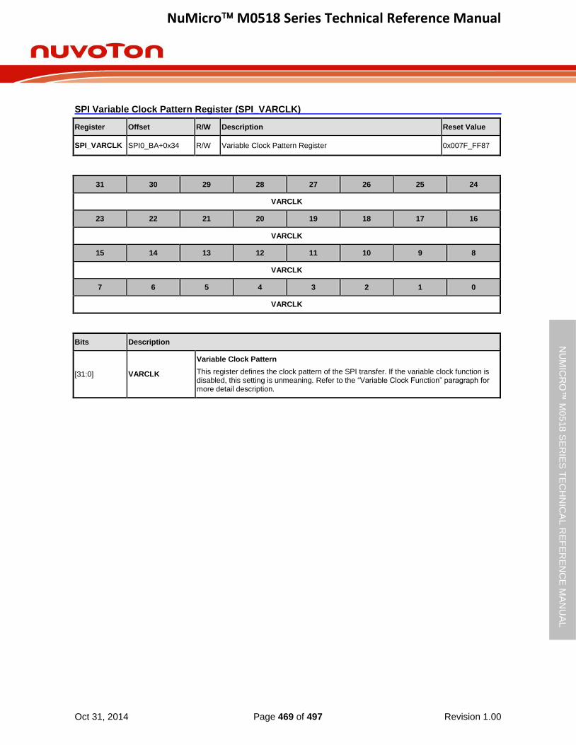
NuMicro M0518 Series Technical Reference Manual
Oct 31, 2014 Page 469 of 497 Revision 1.00
NU
MIC
RO
™ M
0518
SE
RIE
S T
EC
HN
ICA
L R
EF
ER
EN
CE
MA
NU
AL
SPI Variable Clock Pattern Register (SPI_VARCLK)
Register Offset R/W Description Reset Value
SPI_VARCLK SPI0_BA+0x34 R/W Variable Clock Pattern Register 0x007F_FF87
31 30 29 28 27 26 25 24
VARCLK
23 22 21 20 19 18 17 16
VARCLK
15 14 13 12 11 10 9 8
VARCLK
7 6 5 4 3 2 1 0
VARCLK
Bits Description
[31:0] VARCLK
Variable Clock Pattern
This register defines the clock pattern of the SPI transfer. If the variable clock function is disabled, this setting is unmeaning. Refer to the “Variable Clock Function” paragraph for more detail description.
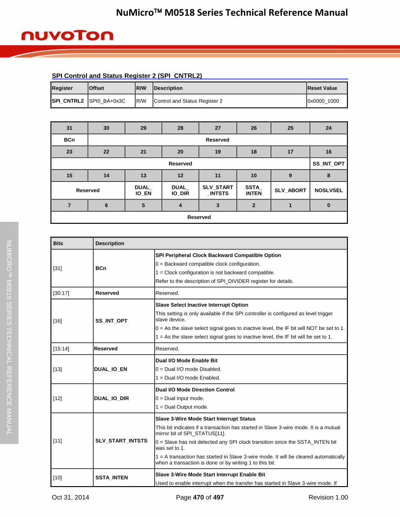
NuMicro M0518 Series Technical Reference Manual
Oct 31, 2014 Page 470 of 497 Revision 1.00
NU
MIC
RO
™ M
0518
SE
RIE
S T
EC
HN
ICA
L R
EF
ER
EN
CE
MA
NU
AL
SPI Control and Status Register 2 (SPI_CNTRL2)
Register Offset R/W Description Reset Value
SPI_CNTRL2 SPI0_BA+0x3C R/W Control and Status Register 2 0x0000_1000
31 30 29 28 27 26 25 24
BCn Reserved
23 22 21 20 19 18 17 16
Reserved SS_INT_OPT
15 14 13 12 11 10 9 8
Reserved DUAL_ IO_EN
DUAL_ IO_DIR
SLV_START_INTSTS
SSTA_ INTEN
SLV_ABORT NOSLVSEL
7 6 5 4 3 2 1 0
Reserved
Bits Description
[31] BCn
SPI Peripheral Clock Backward Compatible Option
0 = Backward compatible clock configuration.
1 = Clock configuration is not backward compatible.
Refer to the description of SPI_DIVIDER register for details.
[30:17] Reserved Reserved.
[16] SS_INT_OPT
Slave Select Inactive Interrupt Option
This setting is only available if the SPI controller is configured as level trigger slave device.
0 = As the slave select signal goes to inactive level, the IF bit will NOT be set to 1.
1 = As the slave select signal goes to inactive level, the IF bit will be set to 1.
[15:14] Reserved Reserved.
[13] DUAL_IO_EN
Dual I/O Mode Enable Bit
0 = Dual I/O mode Disabled.
1 = Dual I/O mode Enabled.
[12] DUAL_IO_DIR
Dual I/O Mode Direction Control
0 = Dual Input mode.
1 = Dual Output mode.
[11] SLV_START_INTSTS
Slave 3-Wire Mode Start Interrupt Status
This bit indicates if a transaction has started in Slave 3-wire mode. It is a mutual mirror bit of SPI_STATUS[11].
0 = Slave has not detected any SPI clock transition since the SSTA_INTEN bit was set to 1.
1 = A transaction has started in Slave 3-wire mode. It will be cleared automatically when a transaction is done or by writing 1 to this bit.
[10] SSTA_INTEN Slave 3-Wire Mode Start Interrupt Enable Bit
Used to enable interrupt when the transfer has started in Slave 3-wire mode. If
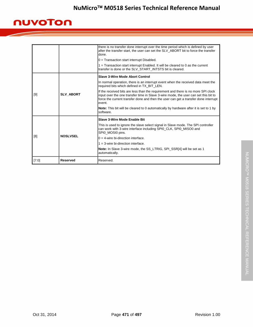
NuMicro M0518 Series Technical Reference Manual
Oct 31, 2014 Page 471 of 497 Revision 1.00
NU
MIC
RO
™ M
0518
SE
RIE
S T
EC
HN
ICA
L R
EF
ER
EN
CE
MA
NU
AL
there is no transfer done interrupt over the time period which is defined by user after the transfer start, the user can set the SLV_ABORT bit to force the transfer done.
0 = Transaction start interrupt Disabled.
1 = Transaction start interrupt Enabled. It will be cleared to 0 as the current transfer is done or the SLV_START_INTSTS bit is cleared.
[9] SLV_ABORT
Slave 3-Wire Mode Abort Control
In normal operation, there is an interrupt event when the received data meet the required bits which defined in TX_BIT_LEN.
If the received bits are less than the requirement and there is no more SPI clock input over the one transfer time in Slave 3-wire mode, the user can set this bit to force the current transfer done and then the user can get a transfer done interrupt event.
Note: This bit will be cleared to 0 automatically by hardware after it is set to 1 by software.
[8] NOSLVSEL
Slave 3-Wire Mode Enable Bit
This is used to ignore the slave select signal in Slave mode. The SPI controller can work with 3-wire interface including SPI0_CLK, SPI0_MISO0 and SPI0_MOSI0 pins.
0 = 4-wire bi-direction interface.
1 = 3-wire bi-direction interface.
Note: In Slave 3-wire mode, the SS_LTRIG, SPI_SSR[4] will be set as 1 automatically.
[7:0] Reserved Reserved.
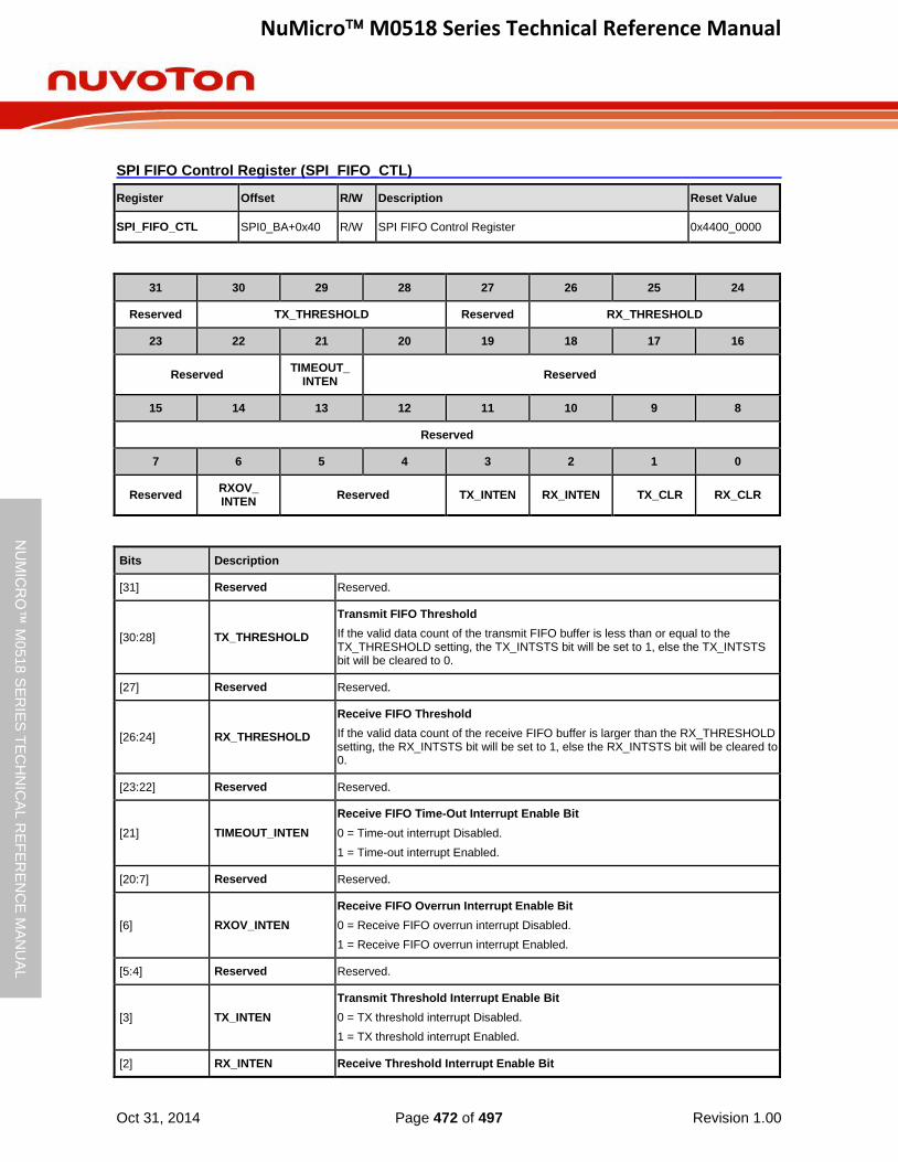
NuMicro M0518 Series Technical Reference Manual
Oct 31, 2014 Page 472 of 497 Revision 1.00
NU
MIC
RO
™ M
0518
SE
RIE
S T
EC
HN
ICA
L R
EF
ER
EN
CE
MA
NU
AL
SPI FIFO Control Register (SPI_FIFO_CTL)
Register Offset R/W Description Reset Value
SPI_FIFO_CTL SPI0_BA+0x40 R/W SPI FIFO Control Register 0x4400_0000
31 30 29 28 27 26 25 24
Reserved TX_THRESHOLD Reserved RX_THRESHOLD
23 22 21 20 19 18 17 16
Reserved TIMEOUT_
INTEN Reserved
15 14 13 12 11 10 9 8
Reserved
7 6 5 4 3 2 1 0
Reserved RXOV_ INTEN
Reserved TX_INTEN RX_INTEN TX_CLR RX_CLR
Bits Description
[31] Reserved Reserved.
[30:28] TX_THRESHOLD
Transmit FIFO Threshold
If the valid data count of the transmit FIFO buffer is less than or equal to the TX_THRESHOLD setting, the TX_INTSTS bit will be set to 1, else the TX_INTSTS bit will be cleared to 0.
[27] Reserved Reserved.
[26:24] RX_THRESHOLD
Receive FIFO Threshold
If the valid data count of the receive FIFO buffer is larger than the RX_THRESHOLD setting, the RX_INTSTS bit will be set to 1, else the RX_INTSTS bit will be cleared to 0.
[23:22] Reserved Reserved.
[21] TIMEOUT_INTEN
Receive FIFO Time-Out Interrupt Enable Bit
0 = Time-out interrupt Disabled.
1 = Time-out interrupt Enabled.
[20:7] Reserved Reserved.
[6] RXOV_INTEN
Receive FIFO Overrun Interrupt Enable Bit
0 = Receive FIFO overrun interrupt Disabled.
1 = Receive FIFO overrun interrupt Enabled.
[5:4] Reserved Reserved.
[3] TX_INTEN
Transmit Threshold Interrupt Enable Bit
0 = TX threshold interrupt Disabled.
1 = TX threshold interrupt Enabled.
[2] RX_INTEN Receive Threshold Interrupt Enable Bit
NuMicro M0518 Series Technical Reference Manual
Oct 31, 2014 Page 473 of 497 Revision 1.00
NU
MIC
RO
™ M
0518
SE
RIE
S T
EC
HN
ICA
L R
EF
ER
EN
CE
MA
NU
AL
0 = RX threshold interrupt Disabled.
1 = RX threshold interrupt Enabled.
[1] TX_CLR
Clear Transmit FIFO Buffer
0 = No effect.
1 = Clear transmit FIFO buffer. The TX_FULL flag will be cleared to 0 and the TX_EMPTY flag will be set to 1. This bit will be cleared to 0 by hardware after it is set to 1 by software.
[0] RX_CLR
Clear Receive FIFO Buffer
0 = No effect.
1 = Clear receive FIFO buffer. The RX_FULL flag will be cleared to 0 and the RX_EMPTY flag will be set to 1. This bit will be cleared to 0 by hardware after it is set to 1 by software.
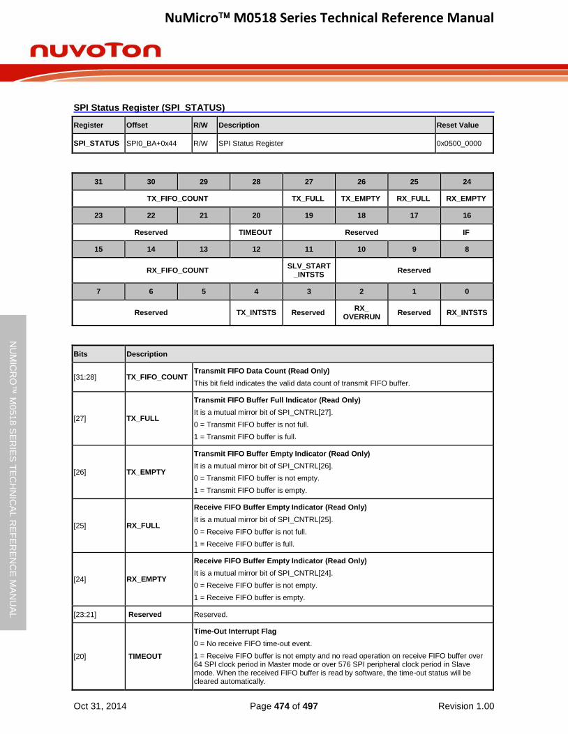
NuMicro M0518 Series Technical Reference Manual
Oct 31, 2014 Page 474 of 497 Revision 1.00
NU
MIC
RO
™ M
0518
SE
RIE
S T
EC
HN
ICA
L R
EF
ER
EN
CE
MA
NU
AL
SPI Status Register (SPI_STATUS)
Register Offset R/W Description Reset Value
SPI_STATUS SPI0_BA+0x44 R/W SPI Status Register 0x0500_0000
31 30 29 28 27 26 25 24
TX_FIFO_COUNT TX_FULL TX_EMPTY RX_FULL RX_EMPTY
23 22 21 20 19 18 17 16
Reserved TIMEOUT Reserved IF
15 14 13 12 11 10 9 8
RX_FIFO_COUNT SLV_START
_INTSTS Reserved
7 6 5 4 3 2 1 0
Reserved TX_INTSTS Reserved RX_
OVERRUN Reserved RX_INTSTS
Bits Description
[31:28] TX_FIFO_COUNT Transmit FIFO Data Count (Read Only)
This bit field indicates the valid data count of transmit FIFO buffer.
[27] TX_FULL
Transmit FIFO Buffer Full Indicator (Read Only)
It is a mutual mirror bit of SPI_CNTRL[27].
0 = Transmit FIFO buffer is not full.
1 = Transmit FIFO buffer is full.
[26] TX_EMPTY
Transmit FIFO Buffer Empty Indicator (Read Only)
It is a mutual mirror bit of SPI_CNTRL[26].
0 = Transmit FIFO buffer is not empty.
1 = Transmit FIFO buffer is empty.
[25] RX_FULL
Receive FIFO Buffer Empty Indicator (Read Only)
It is a mutual mirror bit of SPI_CNTRL[25].
0 = Receive FIFO buffer is not full.
1 = Receive FIFO buffer is full.
[24] RX_EMPTY
Receive FIFO Buffer Empty Indicator (Read Only)
It is a mutual mirror bit of SPI_CNTRL[24].
0 = Receive FIFO buffer is not empty.
1 = Receive FIFO buffer is empty.
[23:21] Reserved Reserved.
[20] TIMEOUT
Time-Out Interrupt Flag
0 = No receive FIFO time-out event.
1 = Receive FIFO buffer is not empty and no read operation on receive FIFO buffer over 64 SPI clock period in Master mode or over 576 SPI peripheral clock period in Slave mode. When the received FIFO buffer is read by software, the time-out status will be cleared automatically.

NuMicro M0518 Series Technical Reference Manual
Oct 31, 2014 Page 475 of 497 Revision 1.00
NU
MIC
RO
™ M
0518
SE
RIE
S T
EC
HN
ICA
L R
EF
ER
EN
CE
MA
NU
AL
Note: This bit will be cleared by writing 1 to itself.
[19:17] Reserved Reserved.
[16] IF
SPI Unit Transfer Interrupt Flag
It is a mutual mirror bit of SPI_CNTRL[16].
0 = No transaction has been finished since this bit was cleared to 0.
1 = SPI controller has finished one unit transfer.
Note: This bit will be cleared by writing 1 to itself.
[15:12] RX_FIFO_COUNT Receive FIFO Data Count (Read Only)
This bit field indicates the valid data count of receive FIFO buffer.
[11] SLV_START_INTSTS
Slave Start Interrupt Status
It is used to dedicate if a transaction has started in Slave 3-wire mode. It is a mutual mirror bit of SPI_CNTRL2[11].
0 = Slave has not detected any SPI clock transition since the SSTA_INTEN bit was set to 1.
1 = A transaction has started in Slave 3-wire mode. It will be cleared as a transaction is done or by writing 1 to this bit.
[10:5] Reserved Reserved.
[4] TX_INTSTS
Transmit FIFO Threshold Interrupt Status (Read Only)
0 = The valid data count within the transmit FIFO buffer is larger than the setting value of TX_THRESHOLD.
1 = The valid data count within the transmit FIFO buffer is less than or equal to the setting value of TX_THRESHOLD.
Note: If TX_INTEN = 1 and TX_INTSTS = 1, the SPI controller will generate a SPI interrupt request.
[3] Reserved Reserved.
[2] RX_OVERRUN
Receive FIFO Overrun Status
When the receive FIFO buffer is full, the follow-up data will be dropped and this bit will be set to 1.
Note: This bit will be cleared by writing 1 to itself.
[1] Reserved Reserved.
[0] RX_INTSTS
Receive FIFO Threshold Interrupt Status (Read Only)
0 = The valid data count within the Rx FIFO buffer is less than or equal to the setting value of RX_THRESHOLD.
1 = The valid data count within the receive FIFO buffer is larger than the setting value of RX_THRESHOLD.
Note: If RX_INTEN = 1 and RX_INTSTS = 1, the SPI controller will generate a SPI interrupt request.

NuMicro M0518 Series Technical Reference Manual
Oct 31, 2014 Page 476 of 497 Revision 1.00
NU
MIC
RO
™ M
0518
SE
RIE
S T
EC
HN
ICA
L R
EF
ER
EN
CE
MA
NU
AL
6.14 Analog-to-Digital Converter (ADC)
6.14.1 Overview
The NuMicro M0518 series contains one 12-bit successive approximation analog-to-digital converters (SAR A/D converter) with 8 input channels. The A/D converter supports three operation modes: single, single-cycle scan and continuous scan mode. The A/D converter can be started by software, PWM, BPWM trigger and external STADC pin.
6.14.2 Features
Analog input voltage range: 0~VREF
12-bit resolution and 10-bit accuracy is guaranteed
Up to 8 single-end analog input channels or 4 differential analog input channels
Up to 1 MSPS conversion rate (chip working at 5V)
Three operating modes
- Single mode: A/D conversion is performed one time on a specified channel
- Single-cycle scan mode: A/D conversion is performed one cycle on all specified channels with the sequence from the smallest numbered channel to the largest numbered channel
- Continuous scan mode: A/D converter continuously performs Single-cycle scan mode until software stops A/D conversion
An A/D conversion can be started by:
- Writing 1 to ADST bit (ADCR[11])through software
- PWM and BPWM trigger
- External pin STADC
Conversion results are held in data registers for each channel with valid and overrun indicators
Supports two set digital comparators. The conversion result can be compared with specify value and user can select whether to generate an interrupt when conversion result matches the compare register setting
Channel 7 supports 2 input sources: external analog voltage, and internal Band-gap voltage
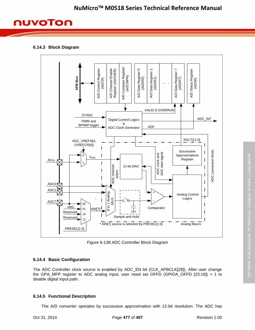
NuMicro M0518 Series Technical Reference Manual
Oct 31, 2014 Page 477 of 497 Revision 1.00
NU
MIC
RO
™ M
0518
SE
RIE
S T
EC
HN
ICA
L R
EF
ER
EN
CE
MA
NU
AL
6.14.3 Block Diagram
12-bit DAC
A/D
Sta
tus R
eg
iste
r
(AD
SR
) Analog Control
Logics
Successive
Approximations
Register
A/D
Da
ta R
eg
iste
r 0
(AD
DR
0)
A/D
Da
ta R
eg
iste
r 1
(AD
DR
1)
A/D
Da
ta R
eg
iste
r 7
(AD
DR
7)
: .
+
-
Digital Control Logics
&
ADC Clock Generator
A/D
Co
ntr
ol R
eg
iste
r
(AD
CR
)
A/D
Ch
an
ne
l E
na
ble
Re
gis
ter
(AD
CH
ER
)
A/D
Co
mp
are
Re
gis
ter
(AD
CM
PR
)
...
ADC0
ADC1
AIN[7]* 8 to
1 A
na
log
MU
X
Sample and Hold
Comparator
RSLT[11:0]
ADC_INTSTADC
Analog Macro
AD
C c
lock a
nd
AD
C s
tart
sig
na
l
VREF
AD
C c
ha
nn
el
se
lect
AP
B B
us
VALID & OVERRUN
ADF
* AIN[7] source is selected by PRESEL[1:0]
ADC7
VBG00
01
PRESEL[1:0]
Reserved
Reserved10
11
AD
C c
on
ve
rsio
n f
inis
h
PWM and
BPWM trigger
...
0
1AVDD
ADC_VREFSEL
(VREFCR[4])
Figure 6-138 ADC Controller Block Diagram
6.14.4 Basic Configuration
The ADC Controller clock source is enabled by ADC_EN bit (CLK_APBCLK[28]). After user change the GPA_MFP register to ADC analog input, user need set OFFD (GPIOA_OFFD [23:16]) = 1 to disable digital input path.
6.14.5 Functional Description
The A/D converter operates by successive approximation with 12-bit resolution. The ADC has
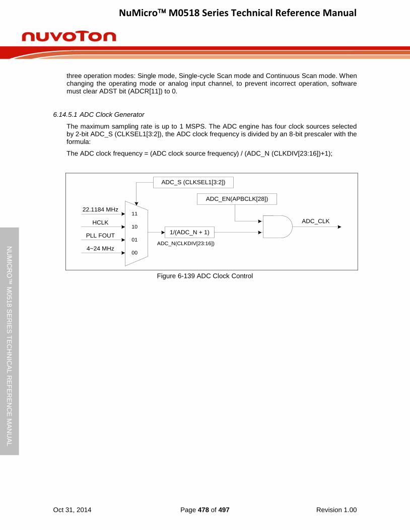
NuMicro M0518 Series Technical Reference Manual
Oct 31, 2014 Page 478 of 497 Revision 1.00
NU
MIC
RO
™ M
0518
SE
RIE
S T
EC
HN
ICA
L R
EF
ER
EN
CE
MA
NU
AL
three operation modes: Single mode, Single-cycle Scan mode and Continuous Scan mode. When changing the operating mode or analog input channel, to prevent incorrect operation, software must clear ADST bit (ADCR[11]) to 0.
6.14.5.1 ADC Clock Generator
The maximum sampling rate is up to 1 MSPS. The ADC engine has four clock sources selected by 2-bit ADC_S (CLKSEL1[3:2]), the ADC clock frequency is divided by an 8-bit prescaler with the formula:
The ADC clock frequency = (ADC clock source frequency) / (ADC_N (CLKDIV[23:16])+1);
11
10
01
00
PLL FOUT
4~24 MHz
22.1184 MHz
ADC_S (CLKSEL1[3:2])
ADC_EN(APBCLK[28])
ADC_CLK
1/(ADC_N + 1)
ADC_N(CLKDIV[23:16])
HCLK
Figure 6-139 ADC Clock Control
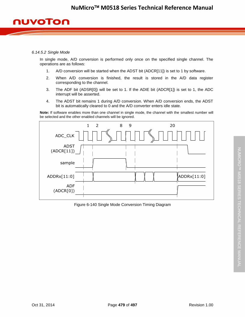
NuMicro M0518 Series Technical Reference Manual
Oct 31, 2014 Page 479 of 497 Revision 1.00
NU
MIC
RO
™ M
0518
SE
RIE
S T
EC
HN
ICA
L R
EF
ER
EN
CE
MA
NU
AL
6.14.5.2 Single Mode
In single mode, A/D conversion is performed only once on the specified single channel. The operations are as follows:
1. A/D conversion will be started when the ADST bit (ADCR[11]) is set to 1 by software.
2. When A/D conversion is finished, the result is stored in the A/D data register corresponding to the channel.
3. The ADF bit (ADSR[0]) will be set to 1. If the ADIE bit (ADCR[1]) is set to 1, the ADC interrupt will be asserted.
4. The ADST bit remains 1 during A/D conversion. When A/D conversion ends, the ADST bit is automatically cleared to 0 and the A/D converter enters idle state.
Note: If software enables more than one channel in single mode, the channel with the smallest number will
be selected and the other enabled channels will be ignored.
sample
ADST(ADCR[11])
ADF(ADCR[0])
1 2 98 20
ADDRx[11:0]
ADC_CLK
ADDRx[11:0]
Figure 6-140 Single Mode Conversion Timing Diagram
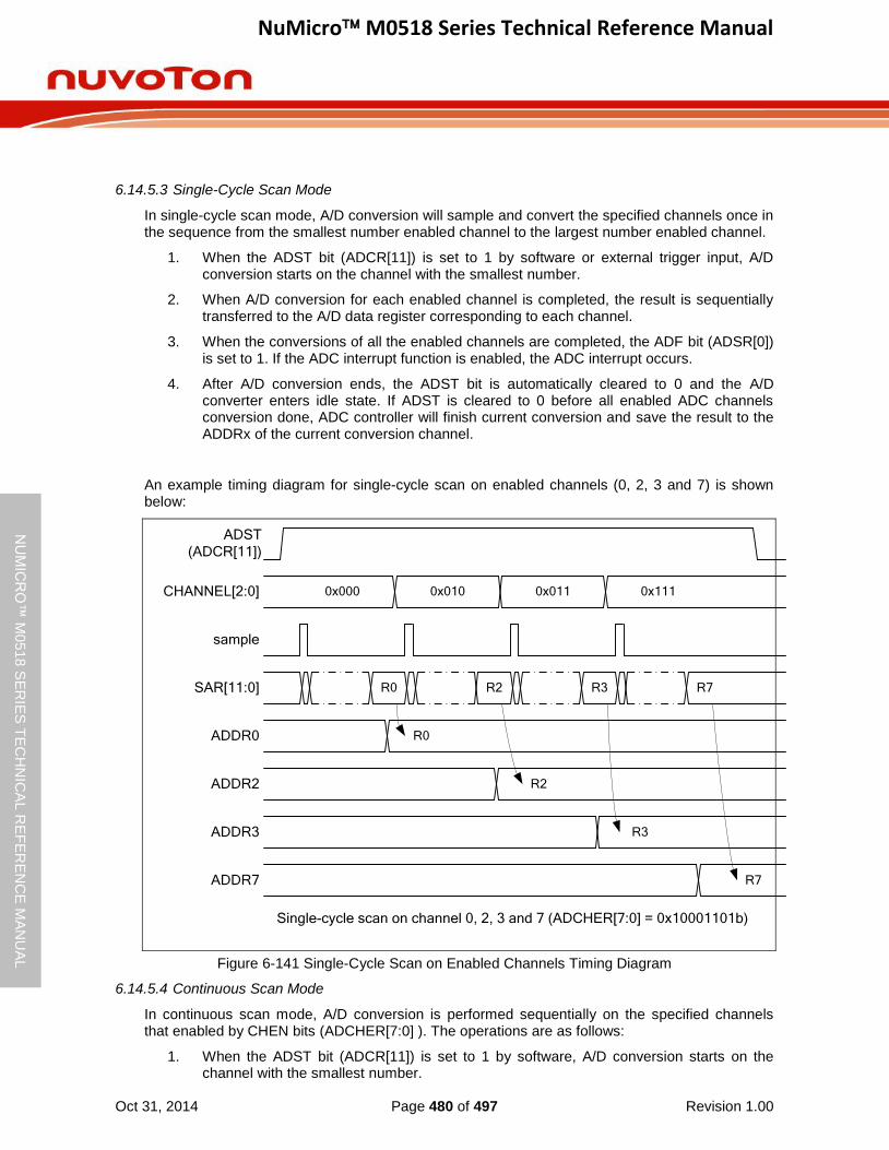
NuMicro M0518 Series Technical Reference Manual
Oct 31, 2014 Page 480 of 497 Revision 1.00
NU
MIC
RO
™ M
0518
SE
RIE
S T
EC
HN
ICA
L R
EF
ER
EN
CE
MA
NU
AL
6.14.5.3 Single-Cycle Scan Mode
In single-cycle scan mode, A/D conversion will sample and convert the specified channels once in the sequence from the smallest number enabled channel to the largest number enabled channel.
1. When the ADST bit (ADCR[11]) is set to 1 by software or external trigger input, A/D conversion starts on the channel with the smallest number.
2. When A/D conversion for each enabled channel is completed, the result is sequentially transferred to the A/D data register corresponding to each channel.
3. When the conversions of all the enabled channels are completed, the ADF bit (ADSR[0]) is set to 1. If the ADC interrupt function is enabled, the ADC interrupt occurs.
4. After A/D conversion ends, the ADST bit is automatically cleared to 0 and the A/D converter enters idle state. If ADST is cleared to 0 before all enabled ADC channels conversion done, ADC controller will finish current conversion and save the result to the ADDRx of the current conversion channel.
An example timing diagram for single-cycle scan on enabled channels (0, 2, 3 and 7) is shown below:
ADST
(ADCR[11])
sample
CHANNEL[2:0] 0x000 0x010 0x011 0x111
ADDR0
ADDR2
ADDR3
ADDR7
Single-cycle scan on channel 0, 2, 3 and 7 (ADCHER[7:0] = 0x10001101b)
SAR[11:0] R0
R0
R2 R3 R7
R2
R3
R7
Figure 6-141 Single-Cycle Scan on Enabled Channels Timing Diagram
6.14.5.4 Continuous Scan Mode
In continuous scan mode, A/D conversion is performed sequentially on the specified channels that enabled by CHEN bits (ADCHER[7:0] ). The operations are as follows:
1. When the ADST bit (ADCR[11]) is set to 1 by software, A/D conversion starts on the channel with the smallest number.
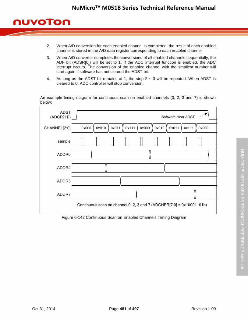
NuMicro M0518 Series Technical Reference Manual
Oct 31, 2014 Page 481 of 497 Revision 1.00
NU
MIC
RO
™ M
0518
SE
RIE
S T
EC
HN
ICA
L R
EF
ER
EN
CE
MA
NU
AL
2. When A/D conversion for each enabled channel is completed, the result of each enabled channel is stored in the A/D data register corresponding to each enabled channel.
3. When A/D converter completes the conversions of all enabled channels sequentially, the ADF bit (ADSR[0]) will be set to 1. If the ADC interrupt function is enabled, the ADC interrupt occurs. The conversion of the enabled channel with the smallest number will start again if software has not cleared the ADST bit.
4. As long as the ADST bit remains at 1, the step 2 ~ 3 will be repeated. When ADST is cleared to 0, ADC controller will stop conversion.
An example timing diagram for continuous scan on enabled channels (0, 2, 3 and 7) is shown below:
ADST
(ADCR[11])
sample
CHANNEL[2:0] 0x000 0x010 0x011 0x111 0x000 0x010 0x011 0x111 0x000
ADDR0
ADDR2
ADDR3
ADDR7
Software clear ADST
Continuous scan on channel 0, 2, 3 and 7 (ADCHER[7:0] = 0x10001101b)
Figure 6-142 Continuous Scan on Enabled Channels Timing Diagram
NuMicro M0518 Series Technical Reference Manual
Oct 31, 2014 Page 482 of 497 Revision 1.00
NU
MIC
RO
™ M
0518
SE
RIE
S T
EC
HN
ICA
L R
EF
ER
EN
CE
MA
NU
AL
6.14.5.5 External trigger Input Sampling and A/D Conversion Time
In single-cycle scan mode, A/D conversion can be triggered by external pin request. When the TRGEN (ADCR[8]) is set to high to enable ADC external trigger function, setting the TRGS bits (ADCR[5:4]) to 00b is to select external trigger input from the STADC pin. Software can set TRGCOND (ADCR[7:6]) to select trigger condition is falling/rising edge or low/high level. If level trigger condition is selected, the STADC pin must be kept at defined state at least 8 PCLKs. The ADST bit will be set to 1 at the 9th PCLK and start to conversion. Conversion is continuous if external trigger input is kept at active state in level trigger mode. It is stopped only when external condition trigger condition disappears. If edge trigger condition is selected, the high and low state must be kept at least 4 PLCKs. Pulse that is shorter than this specification will be ignored.
6.14.5.6 PWM and BPWM trigger
In single-cycle scan mode, the PWM and BPWM can be the trigger source of ADC by setting the TRGEN (ADCR[8]) to 1 and the TRGS (ADCR[5:4]) to 11b.
When PWM enables trigger ADC function, the PWM will generate a trigger signal to ADC when trigger events happened, BPWM have the same behavior. PWM and BPWM trigger events please refer to their corresponding section.
6.14.5.7 Conversion Result Monitor by Compare Function
The ADC controller provide two sets of compare register ADCMPR0 and ADCMPR1, to monitor maximum two specified channels conversion result from A/D conversion controller, refer to Figure 6-143. Software can select which channel to be monitored by set CMPCH (ADCMPR0/1[5:3]) and CMPCOND bit (ADCMPR0/1[2]) is used to check conversion result is less than specify value or greater than (equal to) value specified in CMPD (ADCMPR0/1 [27:16]). When the conversion of the channel specified by CMPCH is completed, the comparing action will be triggered one time automatically. When the compare result meets the setting, compare match counter will increase 1, otherwise, the compare match counter will be cleared to 0. It means the comparing data must be successively matched with the compare condition. Once any comparing data does not match during the comparing, the compare match counter will clear to 0. When counter value reach the setting of (CMPMATCNT (ADCMPR0/1 [11:8])+1) then CMPF0/1 bit (ADSR[1]/[2]) will be set to 1, if CMPIE bit (ADCMPR0/1 [1]) is set then an ADC_INT interrupt request is generated. Software can use it to monitor the external analog input pin voltage transition in scan mode without imposing a load on software. Detailed logics diagram is shown below:

NuMicro M0518 Series Technical Reference Manual
Oct 31, 2014 Page 483 of 497 Revision 1.00
NU
MIC
RO
™ M
0518
SE
RIE
S T
EC
HN
ICA
L R
EF
ER
EN
CE
MA
NU
AL
12-bit
ComparatorRSLT >=CMPD
RSLT < CMPD
CMPCOND(ADCMPRx[2])
1
0 CMPFx
(ADSR[x+1])
A/D
analog
macro
Channel
Addr. 8
to
1
An
alo
g
MU
X
Match
Counter
CMPMATCNT
(ADCMPRx[11:8])
AIN[0]
AIN[7]
……
CHANNEL(ADSR[6:4])
CMPCH(ADCMPRx[5:3])
ADDRx[11:0]
CMPD(ADCMPRx[27:16])
Note:
CMPD=ADCMPRx[27:16]
RSLT=ADDRx[11:0]
x=0,1
Figure 6-143 A/D Conversion Result Monitor Logics Diagram
6.14.5.8 Interrupt Sources
There are three interrupt sources of ADC interrupt. When an ADC operation mode finishes its conversion, the A/D conversion end flag, ADF, will be set to 1. The CMPF0 (ADSR[1]) and CMPF1 (ADSR[2]) are the compare flags of compare function. When the conversion result meets the settings of ADCMPR0/1, the corresponding flag will be set to 1. When one of the flags, ADF (ADSR[0]), CMPF0 and CMPF1, is set to 1 and the corresponding interrupt enable bit, ADIE (ADCR[1]) and CMPIE (ADCMPR0/1[1]), is set to 1, the ADC interrupt will be asserted. Software can clear the flag to revoke the interrupt request.
CMPF0(ADSR[1])
CMPIE(ADCMPR0[1])
CMPF1(ADSR[2])
CMPIE(ADCMPR1[1])
ADC_INT
ADF(ADSR[0])
ADIE(ADCR[1])
Figure 6-144 A/D Controller Interrupt
NuMicro M0518 Series Technical Reference Manual
Oct 31, 2014 Page 484 of 497 Revision 1.00
NU
MIC
RO
™ M
0518
SE
RIE
S T
EC
HN
ICA
L R
EF
ER
EN
CE
MA
NU
AL
6.14.6 Register Map
R: read only, W: write only, R/W: both read and write
Register Offset R/W Description Reset Value
ADC Base Address:
ADC_BA = 0x400E_0000
ADDR0 ADC_BA+0x00 R ADC Data Register 0 0x0000_0000
ADDR1 ADC_BA+0x04 R ADC Data Register 1 0x0000_0000
ADDR2 ADC_BA+0x08 R ADC Data Register 2 0x0000_0000
ADDR3 ADC_BA+0x0C R ADC Data Register 3 0x0000_0000
ADDR4 ADC_BA+0x10 R ADC Data Register 4 0x0000_0000
ADDR5 ADC_BA+0x14 R ADC Data Register 5 0x0000_0000
ADDR6 ADC_BA+0x18 R ADC Data Register 6 0x0000_0000
ADDR7 ADC_BA+0x1C R ADC Data Register 7 0x0000_0000
ADCR ADC_BA+0x20 R/W ADC Control Register 0x0000_0000
ADCHER ADC_BA+0x24 R/W ADC Channel Enable Register 0x0000_0000
ADCMPR0 ADC_BA+0x28 R/W ADC Compare Register 0 0x0000_0000
ADCMPR1 ADC_BA+0x2C R/W ADC Compare Register 1 0x0000_0000
ADSR ADC_BA+0x30 R/W ADC Status Register 0x0000_0000
NuMicro M0518 Series Technical Reference Manual
Oct 31, 2014 Page 485 of 497 Revision 1.00
NU
MIC
RO
™ M
0518
SE
RIE
S T
EC
HN
ICA
L R
EF
ER
EN
CE
MA
NU
AL
6.14.7 Register Description
ADC Data Registers (ADDR0 ~ ADDR7)
Register Offset R/W Description Reset Value
ADDR0 ADC_BA+0x00 R ADC Data Register 0 0x0000_0000
ADDR1 ADC_BA+0x04 R ADC Data Register 1 0x0000_0000
ADDR2 ADC_BA+0x08 R ADC Data Register 2 0x0000_0000
ADDR3 ADC_BA+0x0C R ADC Data Register 3 0x0000_0000
ADDR4 ADC_BA+0x10 R ADC Data Register 4 0x0000_0000
ADDR5 ADC_BA+0x14 R ADC Data Register 5 0x0000_0000
ADDR6 ADC_BA+0x18 R ADC Data Register 6 0x0000_0000
ADDR7 ADC_BA+0x1C R ADC Data Register 7 0x0000_0000
31 30 29 28 27 26 25 24
Reserved
23 22 21 20 19 18 17 16
Reserved VALID OVERRUN
15 14 13 12 11 10 9 8
RSLT
7 6 5 4 3 2 1 0
RSLT
Bits Description
[31:18] Reserved Reserved.
[17] VALID
Valid Flag
0 = Data in RSLT bits (ADDRx[15:0], x=0~7) is not valid.
1 = Data in RSLT bits (ADDRx[15:0], x=0~7) is valid.
This bit is set to 1 when corresponding channel analog input conversion is completed and cleared by hardware after ADDR register is read.
This is a read only bit.
[16] OVERRUN
Overrun Flag
0 = Data in RSLT (ADDRx[15:0], x=0~7) is recent conversion result.
1 = Data in RSLT (ADDRx[15:0], x=0~7) is overwritten.
If converted data in RSLT has not been read before new conversion result is loaded to this register, OVERRUN is set to 1 and previous conversion result is gone. It is cleared by hardware after ADDR register is read.
This is a read only bit.
NuMicro M0518 Series Technical Reference Manual
Oct 31, 2014 Page 486 of 497 Revision 1.00
NU
MIC
RO
™ M
0518
SE
RIE
S T
EC
HN
ICA
L R
EF
ER
EN
CE
MA
NU
AL
[15:0] RSLT
A/D Conversion Result
This field contains conversion result of ADC.
When DMOF bit (ADCR[31]) set to 0, 12-bit ADC conversion result with unsigned format will be filled in RSLT (ADDRx[11:0], x=0~7) and zero will be filled in RSLT (ADDRx[15:12], x=0~7).
When DMOF bit (ADCR[31]) set to 1, 12-bit ADC conversion result with 2’complement format will be filled in RSLT(ADDRx[11:0], x=0~7) and signed bits to will be filled in RSLT (ADDRx[15:12], x=0~7).
Single-end Input voltage
Vin (V)
0000_0000_0000
ADC result in RSLT
(ADDRx[11:0], x=0~7)
0000_0000_0001
0000_0000_0010
1111_1111_1111
1111_1111_1110
1111_1111_1101
1 LSB Vref - 1 LSB
1 LSB = Vref/4096
Figure 6-145 ADC Single-end Input Conversion Voltage and Conversion Result Mapping
0000_0000_0000
ADC result in RSLT
(ADDRx[11:0], x=0~7)
(DMOF (ADCR[31]) = 0)
0000_0000_0001
0000_0000_0010
1111_1111_1111
1111_1111_1110
1111_1111_1101
-Vref + 1 LSB Vref - 1 LSB
Differential Input voltage
Vdiff (V)
1000_0000_0001
1000_0000_0000
0111_1111_1111
0
1 LSB = Vref/4096
1111_1000_0000_0000
1111_1000_0000_0001
1111_1000_0000_0010
0000_0111_1111_1111
0000_0111_1111_1110
0000_0111_1111_1101
-Vref + 1 LSB Vref - 1 LSB
Differential Input voltage
Vdiff (V)
0000_0000_0000_0001
0000_0000_0000_0000
1111_1111_1111_1111
0
1 LSB = Vref/4096
ADC result in RSLT
(ADDRx[15:0], x=0~7)
(DMOF (ADCR[31]) = 1)
Figure 6-146 ADC Differential Input Conversion Voltage and Conversion Result Mapping
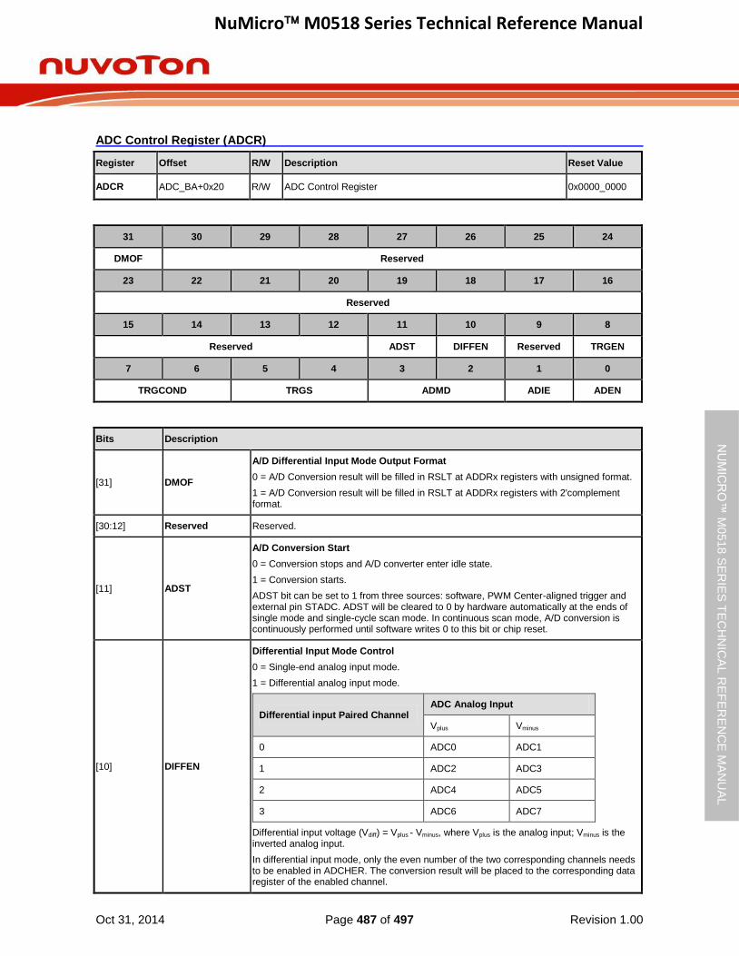
NuMicro M0518 Series Technical Reference Manual
Oct 31, 2014 Page 487 of 497 Revision 1.00
NU
MIC
RO
™ M
0518
SE
RIE
S T
EC
HN
ICA
L R
EF
ER
EN
CE
MA
NU
AL
ADC Control Register (ADCR)
Register Offset R/W Description Reset Value
ADCR ADC_BA+0x20 R/W ADC Control Register 0x0000_0000
31 30 29 28 27 26 25 24
DMOF Reserved
23 22 21 20 19 18 17 16
Reserved
15 14 13 12 11 10 9 8
Reserved ADST DIFFEN Reserved TRGEN
7 6 5 4 3 2 1 0
TRGCOND TRGS ADMD ADIE ADEN
Bits Description
[31] DMOF
A/D Differential Input Mode Output Format
0 = A/D Conversion result will be filled in RSLT at ADDRx registers with unsigned format.
1 = A/D Conversion result will be filled in RSLT at ADDRx registers with 2'complement format.
[30:12] Reserved Reserved.
[11] ADST
A/D Conversion Start
0 = Conversion stops and A/D converter enter idle state.
1 = Conversion starts.
ADST bit can be set to 1 from three sources: software, PWM Center-aligned trigger and external pin STADC. ADST will be cleared to 0 by hardware automatically at the ends of single mode and single-cycle scan mode. In continuous scan mode, A/D conversion is continuously performed until software writes 0 to this bit or chip reset.
[10] DIFFEN
Differential Input Mode Control
0 = Single-end analog input mode.
1 = Differential analog input mode.
Differential input Paired Channel ADC Analog Input
Vplus Vminus
0 ADC0 ADC1
1 ADC2 ADC3
2 ADC4 ADC5
3 ADC6 ADC7
Differential input voltage (Vdiff) = Vplus - Vminus, where Vplus is the analog input; Vminus is the inverted analog input.
In differential input mode, only the even number of the two corresponding channels needs to be enabled in ADCHER. The conversion result will be placed to the corresponding data register of the enabled channel.
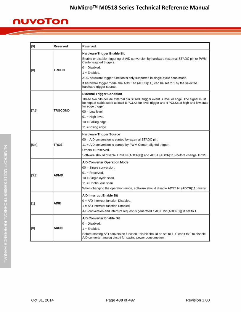
NuMicro M0518 Series Technical Reference Manual
Oct 31, 2014 Page 488 of 497 Revision 1.00
NU
MIC
RO
™ M
0518
SE
RIE
S T
EC
HN
ICA
L R
EF
ER
EN
CE
MA
NU
AL
[9] Reserved Reserved.
[8] TRGEN
Hardware Trigger Enable Bit
Enable or disable triggering of A/D conversion by hardware (external STADC pin or PWM Center-aligned trigger).
0 = Disabled.
1 = Enabled.
ADC hardware trigger function is only supported in single-cycle scan mode.
If hardware trigger mode, the ADST bit (ADCR[11]) can be set to 1 by the selected hardware trigger source.
[7:6] TRGCOND
External Trigger Condition
These two bits decide external pin STADC trigger event is level or edge. The signal must be kept at stable state at least 8 PCLKs for level trigger and 4 PCLKs at high and low state for edge trigger.
00 = Low level.
01 = High level.
10 = Falling edge.
11 = Rising edge.
[5:4] TRGS
Hardware Trigger Source
00 = A/D conversion is started by external STADC pin.
11 = A/D conversion is started by PWM Center-aligned trigger.
Others = Reserved.
Software should disable TRGEN (ADCR[8]) and ADST (ADCR[11]) before change TRGS.
[3:2] ADMD
A/D Converter Operation Mode
00 = Single conversion.
01 = Reserved.
10 = Single-cycle scan.
11 = Continuous scan.
When changing the operation mode, software should disable ADST bit (ADCR[11]) firstly.
[1] ADIE
A/D Interrupt Enable Bit
0 = A/D interrupt function Disabled.
1 = A/D interrupt function Enabled.
A/D conversion end interrupt request is generated if ADIE bit (ADCR[1]) is set to 1.
[0] ADEN
A/D Converter Enable Bit
0 = Disabled.
1 = Enabled.
Before starting A/D conversion function, this bit should be set to 1. Clear it to 0 to disable A/D converter analog circuit for saving power consumption.
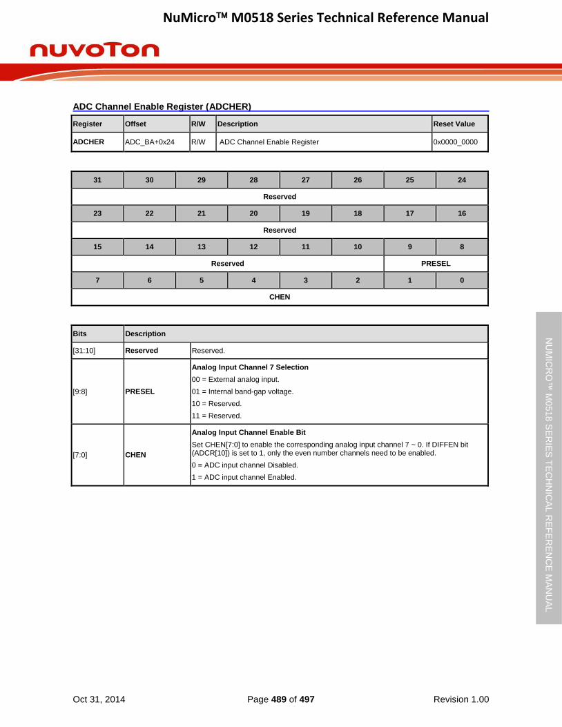
NuMicro M0518 Series Technical Reference Manual
Oct 31, 2014 Page 489 of 497 Revision 1.00
NU
MIC
RO
™ M
0518
SE
RIE
S T
EC
HN
ICA
L R
EF
ER
EN
CE
MA
NU
AL
ADC Channel Enable Register (ADCHER)
Register Offset R/W Description Reset Value
ADCHER ADC_BA+0x24 R/W ADC Channel Enable Register 0x0000_0000
31 30 29 28 27 26 25 24
Reserved
23 22 21 20 19 18 17 16
Reserved
15 14 13 12 11 10 9 8
Reserved PRESEL
7 6 5 4 3 2 1 0
CHEN
Bits Description
[31:10] Reserved Reserved.
[9:8] PRESEL
Analog Input Channel 7 Selection
00 = External analog input.
01 = Internal band-gap voltage.
10 = Reserved.
11 = Reserved.
[7:0] CHEN
Analog Input Channel Enable Bit
Set CHEN[7:0] to enable the corresponding analog input channel 7 ~ 0. If DIFFEN bit (ADCR[10]) is set to 1, only the even number channels need to be enabled.
0 = ADC input channel Disabled.
1 = ADC input channel Enabled.
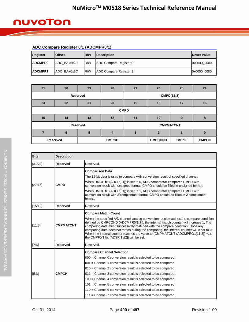
NuMicro M0518 Series Technical Reference Manual
Oct 31, 2014 Page 490 of 497 Revision 1.00
NU
MIC
RO
™ M
0518
SE
RIE
S T
EC
HN
ICA
L R
EF
ER
EN
CE
MA
NU
AL
ADC Compare Register 0/1 (ADCMPR0/1)
Register Offset R/W Description Reset Value
ADCMPR0 ADC_BA+0x28 R/W ADC Compare Register 0 0x0000_0000
ADCMPR1 ADC_BA+0x2C R/W ADC Compare Register 1 0x0000_0000
31 30 29 28 27 26 25 24
Reserved CMPD[11:8]
23 22 21 20 19 18 17 16
CMPD
15 14 13 12 11 10 9 8
Reserved CMPMATCNT
7 6 5 4 3 2 1 0
Reserved CMPCH CMPCOND CMPIE CMPEN
Bits Description
[31:28] Reserved Reserved.
[27:16] CMPD
Comparison Data
The 12-bit data is used to compare with conversion result of specified channel.
When DMOF bit (ADCR[31]) is set to 0, ADC comparator compares CMPD with conversion result with unsigned format. CMPD should be filled in unsigned format.
When DMOF bit (ADCR[31]) is set to 1, ADC comparator compares CMPD with conversion result with 2’complement format. CMPD should be filled in 2’complement format.
[15:12] Reserved Reserved.
[11:8] CMPMATCNT
Compare Match Count
When the specified A/D channel analog conversion result matches the compare condition defined by CMPCOND (ADCMPR0/1[2]), the internal match counter will increase 1, The comparing data must successively matched with the compare condition. Once any comparing data does not match during the comparing, the internal counter will clear to 0. When the internal counter reaches the value to (CMPMATCNT (ADCMPR0/1[11:8]) +1), the CMPF0/1 bit (ADSR[1]/[2]) will be set.
[7:6] Reserved Reserved.
[5:3] CMPCH
Compare Channel Selection
000 = Channel 0 conversion result is selected to be compared.
001 = Channel 1 conversion result is selected to be compared.
010 = Channel 2 conversion result is selected to be compared.
011 = Channel 3 conversion result is selected to be compared.
100 = Channel 4 conversion result is selected to be compared.
101 = Channel 5 conversion result is selected to be compared.
110 = Channel 6 conversion result is selected to be compared.
111 = Channel 7 conversion result is selected to be compared.
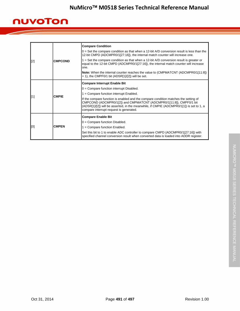
NuMicro M0518 Series Technical Reference Manual
Oct 31, 2014 Page 491 of 497 Revision 1.00
NU
MIC
RO
™ M
0518
SE
RIE
S T
EC
HN
ICA
L R
EF
ER
EN
CE
MA
NU
AL
[2] CMPCOND
Compare Condition
0 = Set the compare condition as that when a 12-bit A/D conversion result is less than the 12-bit CMPD (ADCMPR0/1[27:16]), the internal match counter will increase one.
1 = Set the compare condition as that when a 12-bit A/D conversion result is greater or equal to the 12-bit CMPD (ADCMPR0/1[27:16]), the internal match counter will increase one.
Note: When the internal counter reaches the value to (CMPMATCNT (ADCMPR0/1[11:8]) + 1), the CMPF0/1 bit (ADSR[1]/[2]) will be set.
[1] CMPIE
Compare Interrupt Enable Bit
0 = Compare function interrupt Disabled.
1 = Compare function interrupt Enabled.
If the compare function is enabled and the compare condition matches the setting of CMPCOND (ADCMPR0/1[2]) and CMPMATCNT (ADCMPR0/1[11:8]), CMPF0/1 bit (ADSR[1]/[2]) will be asserted, in the meanwhile, if CMPIE (ADCMPR0/1[1]) is set to 1, a compare interrupt request is generated.
[0] CMPEN
Compare Enable Bit
0 = Compare function Disabled.
1 = Compare function Enabled.
Set this bit to 1 to enable ADC controller to compare CMPD (ADCMPR0/1[27:16]) with specified channel conversion result when converted data is loaded into ADDR register.
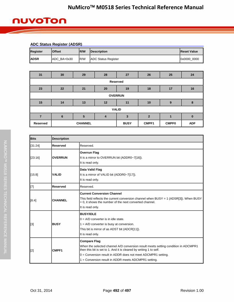
NuMicro M0518 Series Technical Reference Manual
Oct 31, 2014 Page 492 of 497 Revision 1.00
NU
MIC
RO
™ M
0518
SE
RIE
S T
EC
HN
ICA
L R
EF
ER
EN
CE
MA
NU
AL
ADC Status Register (ADSR)
Register Offset R/W Description Reset Value
ADSR ADC_BA+0x30 R/W ADC Status Register 0x0000_0000
31 30 29 28 27 26 25 24
Reserved
23 22 21 20 19 18 17 16
OVERRUN
15 14 13 12 11 10 9 8
VALID
7 6 5 4 3 2 1 0
Reserved CHANNEL BUSY CMPF1 CMPF0 ADF
Bits Description
[31:24] Reserved Reserved.
[23:16] OVERRUN
Overrun Flag
It is a mirror to OVERRUN bit (ADDR0~7[16]).
It is read only.
[15:8] VALID
Data Valid Flag
It is a mirror of VALID bit (ADDR0~7[17]).
It is read only.
[7] Reserved Reserved.
[6:4] CHANNEL
Current Conversion Channel
This field reflects the current conversion channel when BUSY = 1 (ADSR[3]). When BUSY = 0, it shows the number of the next converted channel.
It is read only.
[3] BUSY
BUSY/IDLE
0 = A/D converter is in idle state.
1 = A/D converter is busy at conversion.
This bit is mirror of as ADST bit (ADCR[11]).
It is read only.
[2] CMPF1
Compare Flag
When the selected channel A/D conversion result meets setting condition in ADCMPR1 then this bit is set to 1. And it is cleared by writing 1 to self.
0 = Conversion result in ADDR does not meet ADCMPR1 setting.
1 = Conversion result in ADDR meets ADCMPR1 setting.
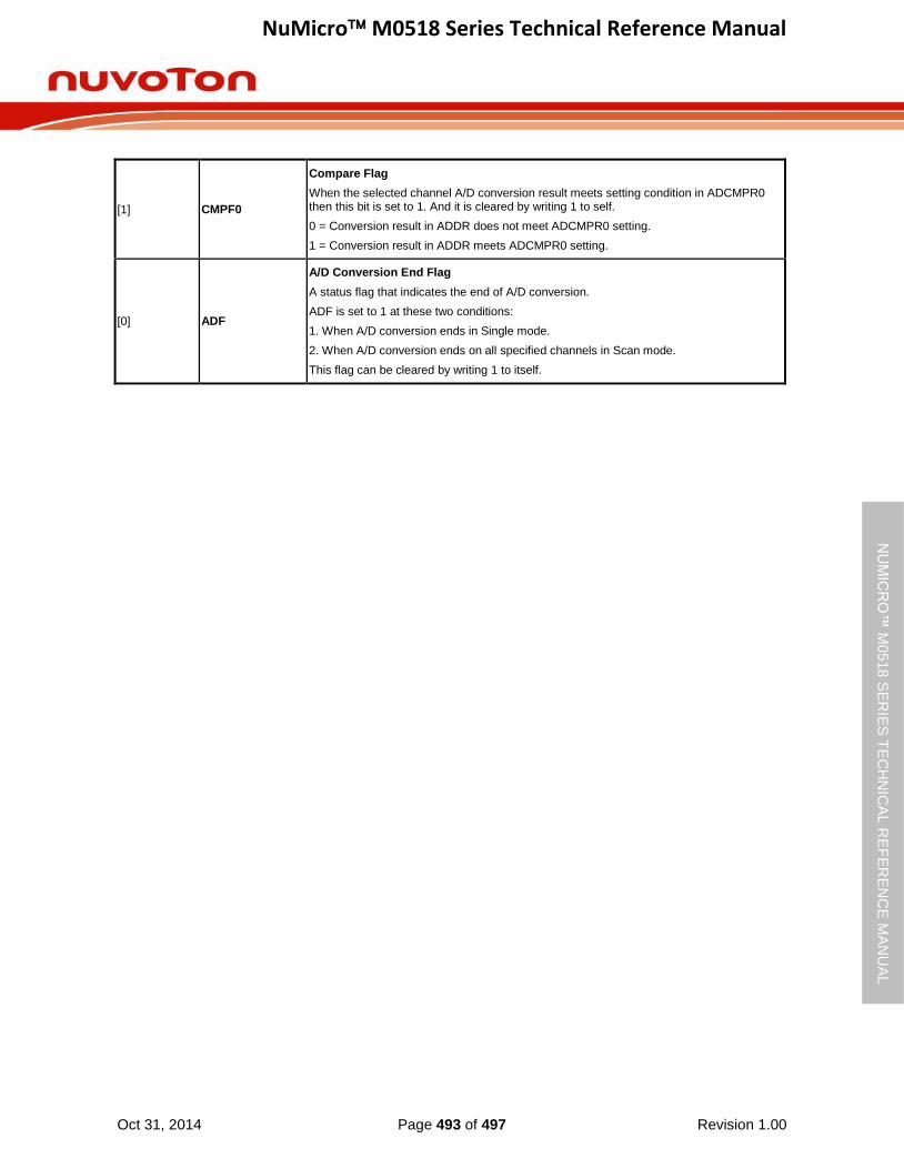
NuMicro M0518 Series Technical Reference Manual
Oct 31, 2014 Page 493 of 497 Revision 1.00
NU
MIC
RO
™ M
0518
SE
RIE
S T
EC
HN
ICA
L R
EF
ER
EN
CE
MA
NU
AL
[1] CMPF0
Compare Flag
When the selected channel A/D conversion result meets setting condition in ADCMPR0 then this bit is set to 1. And it is cleared by writing 1 to self.
0 = Conversion result in ADDR does not meet ADCMPR0 setting.
1 = Conversion result in ADDR meets ADCMPR0 setting.
[0] ADF
A/D Conversion End Flag
A status flag that indicates the end of A/D conversion.
ADF is set to 1 at these two conditions:
1. When A/D conversion ends in Single mode.
2. When A/D conversion ends on all specified channels in Scan mode.
This flag can be cleared by writing 1 to itself.

NuMicro M0518 Series Technical Reference Manual
Oct 31, 2014 Page 494 of 497 Revision 1.00
NU
MIC
RO
™ M
0518
SE
RIE
S T
EC
HN
ICA
L R
EF
ER
EN
CE
MA
NU
AL
7 ELECTRICAL CHARACTERISTICS
For information on the M0518 series electrical characteristics, please refer to NuMicro™ M0518 Series Datasheet.
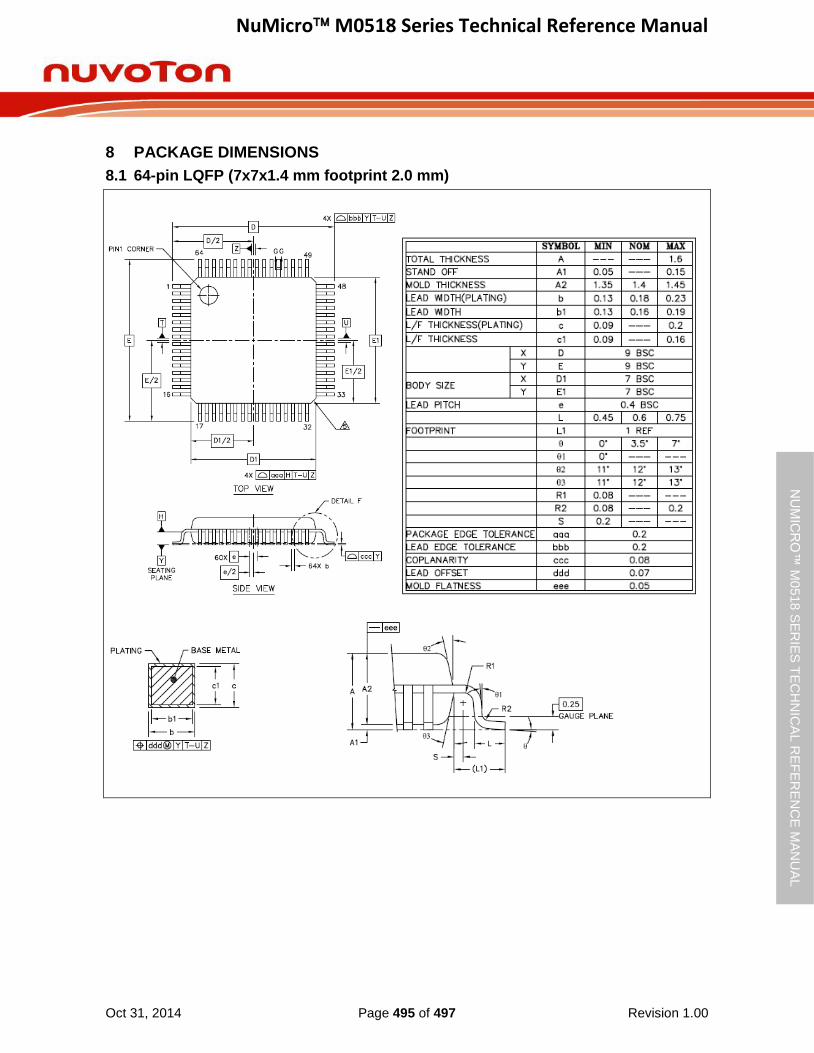
NuMicro M0518 Series Technical Reference Manual
Oct 31, 2014 Page 495 of 497 Revision 1.00
NU
MIC
RO
™ M
0518
SE
RIE
S T
EC
HN
ICA
L R
EF
ER
EN
CE
MA
NU
AL
8 PACKAGE DIMENSIONS
8.1 64-pin LQFP (7x7x1.4 mm footprint 2.0 mm)
NuMicro M0518 Series Technical Reference Manual
Oct 31, 2014 Page 496 of 497 Revision 1.00
NU
MIC
RO
™ M
0518
SE
RIE
S T
EC
HN
ICA
L R
EF
ER
EN
CE
MA
NU
AL
8.2 48-pin LQFP (7x7x1.4 mm footprint 2.0 mm)
NuMicro M0518 Series Technical Reference Manual
Oct 31, 2014 Page 497 of 497 Revision 1.00
NU
MIC
RO
™ M
0518
SE
RIE
S T
EC
HN
ICA
L R
EF
ER
EN
CE
MA
NU
AL
9 REVISION HISTORY
REVISION DATE DESCRIPTION
1.00 Oct. 31, 2014 Preliminary version
Important Notice
Nuvoton Products are neither intended nor warranted for usage in systems or equipment, any malfunction or failure of which may cause loss of human life, bodily injury or severe property damage. Such applications are deemed, “Insecure Usage”.
Insecure usage includes, but is not limited to: equipment for surgical implementation, atomic energy control instruments, airplane or spaceship instruments, the control or operation of dynamic, brake or safety systems designed for vehicular use, traffic signal instruments, all types of safety devices, and other applications intended to support or sustain life.
All Insecure Usage shall be made at customer’s risk, and in the event that third parties lay claims to Nuvoton as a result of customer’s Insecure Usage, customer shall indemnify the damages and liabilities thus incurred by Nuvoton.