NuMicro Family Nano100 Series Datasheet - NuvotonB)_Series_EN_Rev1.08.… · NuMicro® Family...
160
NUMICRO® NANO100 (B) DATASHEET May 31, 2016 Page 1 of 160 Revision 1.08 NANO100 SERIES DATASHEET ARM ® Cortex ® -M 32-bit Microcontroller NuMicro ® Family Nano100 Series Datasheet The information described in this document is the exclusive intellectual property of Nuvoton Technology Corporation and shall not be reproduced without permission from Nuvoton. Nuvoton is providing this document only for reference purposes of NuMicro microcontroller based system design. Nuvoton assumes no responsibility for errors or omissions. All data and specifications are subject to change without notice. For additional information or questions, please contact: Nuvoton Technology Corporation. www.nuvoton.com
Transcript of NuMicro Family Nano100 Series Datasheet - NuvotonB)_Series_EN_Rev1.08.… · NuMicro® Family...

NUMICRO® NANO100 (B) DATASHEET
May 31, 2016 Page 1 of 160 Revision 1.08
NA
NO
10
0 S
ER
IES
DA
TA
SH
EE
T
ARM® Cortex
®-M
32-bit Microcontroller
NuMicro® Family
Nano100 Series
Datasheet
The information described in this document is the exclusive intellectual property of Nuvoton Technology Corporation and shall not be reproduced without permission from Nuvoton.
Nuvoton is providing this document only for reference purposes of NuMicro microcontroller based system design. Nuvoton assumes no responsibility for errors or omissions.
All data and specifications are subject to change without notice.
For additional information or questions, please contact: Nuvoton Technology Corporation.
www.nuvoton.com
NUMICRO® NANO100 (B) DATASHEET
May 31, 2016 Page 2 of 160 Revision 1.08
NA
NO
10
0 S
ER
IES
DA
TA
SH
EE
T
Table of Contents
LIST OF FIGURES ........................................................................................................................... 6 LIST OF TABLES ............................................................................................................................. 7 1 GENERAL DESCRIPTION ..................................................................................................... 8 2 FEATURES ........................................................................................................................... 10
2.1 Nano100 Features – Base Line ................................................................................. 10
2.2 Nano110 Features – LCD Line .................................................................................. 16
2.3 Nano120 Features – USB Connectivity Line.............................................................. 22
2.4 Nano130 Features – Advanced Line .......................................................................... 28
3 PARTS INFORMATION LIST AND PIN CONFIGURATION ................................................ 34 3.1 NuMicro
® Nano100 Series Selection Code ................................................................ 34
3.2 NuMicro® Nano100 Products Selection Guide ........................................................... 35
3.2.1 NuMicro® Nano100 Base Line Selection Guide .............................................................. 35
3.2.2 NuMicro® Nano110 LCD Line Selection Guide ............................................................... 35
3.2.3 NuMicro®
Nano120 USB Connectivity Line Selection Guide .......................................... 35 3.2.4 NuMicro
® Nano130 Advanced Line Selection Guide ...................................................... 36
3.3 Pin Configuration ........................................................................................................ 37
3.3.1 NuMicro® Nano100 Pin Diagrams .................................................................................. 37
3.3.2 NuMicro® Nano110 Pin Diagrams .................................................................................. 40
3.3.3 NuMicro® Nano120 Pin Diagrams .................................................................................. 42
3.3.4 NuMicro® Nano130 Pin Diagrams .................................................................................. 45
3.4 Pin Description ........................................................................................................... 47
3.4.1 NuMicro® Nano100 Pin Description ................................................................................ 47
3.4.2 NuMicro® Nano110 Pin Description ................................................................................ 58
3.4.3 NuMicro® Nano120 Pin Description ................................................................................ 72
3.4.4 NuMicro® Nano130 Pin Description ................................................................................ 83
4 BLOCK DIAGRAM ................................................................................................................ 97 4.1 Nano100 Block Diagram ............................................................................................ 97
4.2 Nano110 Block Diagram ............................................................................................ 98
4.3 Nano120 Block Diagram ............................................................................................ 99
4.4 Nano130 Block Diagram .......................................................................................... 100
5 FUNCTIONAL DESCRIPTION ............................................................................................ 101 5.1 Memory Organization ............................................................................................... 101
5.1.1 Overview ...................................................................................................................... 101 5.1.2 Memory Map ................................................................................................................ 101
5.2 Nested Vectored Interrupt Controller (NVIC) ........................................................... 103
5.2.1 Overview ...................................................................................................................... 103 5.2.2 Features ....................................................................................................................... 103
5.3 System Manager ...................................................................................................... 104
5.3.1 Overview ...................................................................................................................... 104 5.3.2 Features ....................................................................................................................... 104
5.4 Clock Controller ........................................................................................................ 105
5.4.1 Overview ...................................................................................................................... 105

NUMICRO® NANO100 (B) DATASHEET
May 31, 2016 Page 3 of 160 Revision 1.08
NA
NO
10
0 S
ER
IES
DA
TA
SH
EE
T
5.4.2 Features ....................................................................................................................... 105 5.5 Analog to Digital Converter (ADC) ........................................................................... 106
5.5.1 Overview ...................................................................................................................... 106 5.5.2 Features ....................................................................................................................... 106
5.6 Digital to Analog Converter (DAC) ........................................................................... 107
5.6.1 Overview ...................................................................................................................... 107 5.6.2 Features ....................................................................................................................... 107
5.7 DMA Controller ......................................................................................................... 108
5.7.1 Overview ...................................................................................................................... 108 5.7.2 Features ....................................................................................................................... 108
5.8 External Bus Interface .............................................................................................. 110
5.8.1 Overview ...................................................................................................................... 110 5.8.2 Features ....................................................................................................................... 110
5.9 FLASH Memory Controller (FMC) ............................................................................ 111
5.9.1 Overview ...................................................................................................................... 111 5.9.2 Features ....................................................................................................................... 111
5.10 General Purpose I/O Controller ................................................................................ 112
5.10.1 Overview .................................................................................................................... 112 5.10.2 Features ..................................................................................................................... 112
5.11 I2C ............................................................................................................................. 113
5.11.1 Overview .................................................................................................................... 113 5.11.2 Features ..................................................................................................................... 114
5.12 I2S ............................................................................................................................. 115
5.12.1 Overview .................................................................................................................... 115 5.12.2 Features ..................................................................................................................... 115
5.13 LCD Display Driver ................................................................................................... 116
5.13.1 Overview .................................................................................................................... 116 5.13.2 Features ..................................................................................................................... 116
5.14 Pulse Width Modulation (PWM) ............................................................................... 117
5.14.1 Overview .................................................................................................................... 117 5.14.2 Features ..................................................................................................................... 118
5.15 RTC .......................................................................................................................... 119
5.15.1 Overview .................................................................................................................... 119 5.15.2 Features ..................................................................................................................... 119
5.16 Smart Card Host Interface (SC) ............................................................................... 119
5.16.1 Overview .................................................................................................................... 119 5.16.2 Features ..................................................................................................................... 119
5.17 SPI ............................................................................................................................ 121
5.17.1 Overview .................................................................................................................... 121 5.17.2 Features ..................................................................................................................... 121
5.18 Timer Controller ........................................................................................................ 122
5.18.1 Overview .................................................................................................................... 122 5.18.2 Features ..................................................................................................................... 122
5.19 UART Controller ....................................................................................................... 123

NUMICRO® NANO100 (B) DATASHEET
May 31, 2016 Page 4 of 160 Revision 1.08
NA
NO
10
0 S
ER
IES
DA
TA
SH
EE
T
5.19.1 Overview .................................................................................................................... 123 5.19.2 The LIN mode is selected by setting the LIN_EN bit in UART_FUN_SEL register. In LIN mode, one start bit and 8-bit data format with 1-bit stop bit are required in accordance with the LIN standard. Features.............................................................................................................. 124
5.20 USB .......................................................................................................................... 126
5.20.1 Overview .................................................................................................................... 126 5.20.2 Features ..................................................................................................................... 126
5.21 Watchdog Timer Controller ...................................................................................... 127
5.21.1 Overview .................................................................................................................... 127 5.21.2 Features ..................................................................................................................... 127
5.22 Window Watchdog Timer Controller ........................................................................ 128
5.22.1 Overview .................................................................................................................... 128 5.22.2 Features ..................................................................................................................... 128
6 ARM® CORTEX™-M0 CORE ............................................................................................. 129
6.1 Overview................................................................................................................... 129
6.2 Features ................................................................................................................... 129
7 APPLICATION CIRCUIT ..................................................................................................... 131 7.1 LCD Charge Pump ................................................................................................... 131
7.1.1 C-type 1/3 Bias ............................................................................................................. 131 7.1.2 C-type 1/2 Bias ............................................................................................................. 131 7.1.3 Internal R-type .............................................................................................................. 131 7.1.4 External R-type ............................................................................................................. 132
7.2 ADC Application Circuit ............................................................................................ 133
7.2.1 Voltage Reference Source ........................................................................................... 133 7.3 DAC Application Circuit ............................................................................................ 135
7.3.1 Voltage Reference Source ........................................................................................... 135 7.4 Whole Chip Application Circuit ................................................................................. 137
8 POWER COMSUMPTION .................................................................................................. 138 9 ELECTRICAL CHARACTERISTIC ..................................................................................... 139
9.1 Absolute Maximum Ratings...................................................................................... 139
9.2 Nano100/Nano110/Nano120/Nano130 DC Electrical Characteristics ..................... 139
9.3 AC Electrical Characteristics .................................................................................... 145
9.3.1 External Input Clock ..................................................................................................... 145 9.3.2 External 4~24 MHz XTAL Oscillator ............................................................................. 145 9.3.3 External 32.768 kHz Crystal ......................................................................................... 146 9.3.4 Internal 12 MHz Oscillator ............................................................................................ 146 9.3.5 Internal 10 kHz Oscillator ............................................................................................. 146
9.4 Analog Characteristics ............................................................................................. 146
9.4.1 12-bit ADC .................................................................................................................... 146 9.4.2 Brown-out Detector ....................................................................................................... 147 9.4.3 Power-on Reset ............................................................................................................ 148 9.4.4 Temperature Sensor ..................................................................................................... 148 9.4.5 12-bit DAC .................................................................................................................... 148 9.4.6 LCD .............................................................................................................................. 149 9.4.7 Internal Voltage Reference ........................................................................................... 149

NUMICRO® NANO100 (B) DATASHEET
May 31, 2016 Page 5 of 160 Revision 1.08
NA
NO
10
0 S
ER
IES
DA
TA
SH
EE
T
9.4.8 USB PHY Specifications ............................................................................................... 149 9.5 Flash DC Electrical Characteristics .......................................................................... 151
10 PACKAGE DIMENSIONS ................................................................................................... 152 10.1 LQFP128 (14x14x1.4 mm footprint 2.0 mm) ............................................................ 152
10.2 LQFP64 (10x10x1.4 mm footprint 2.0 mm) .............................................................. 153
10.3 LQFP64 (7x7x1.4 mm footprint 2.0 mm) .................................................................. 154
10.4 LQFP48 (7x7x1.4 mm footprint 2.0 mm) .................................................................. 156
10.5 QFN48 (7x7x0.85 mm) ............................................................................................. 157
11 REVISION HISTORY .......................................................................................................... 158

NUMICRO® NANO100 (B) DATASHEET
May 31, 2016 Page 6 of 160 Revision 1.08
NA
NO
10
0 S
ER
IES
DA
TA
SH
EE
T
LIST OF FIGURES Figure 3‑1 NuMicro
® Nano100 Series Selection Code .................................................................. 34
Figure 3‑2 NuMicro® Nano100 LQFP 128-pin Diagram ................................................................ 37
Figure 3‑3 NuMicro® Nano100 LQFP 64-pin Diagram .................................................................. 38
Figure 3‑4 NuMicro®
Nano100 LQFP 48-pin Diagram ................................................................... 39
Figure 3‑5 NuMicro®
Nano110 LQFP 128-pin Diagram ................................................................. 40
Figure 3‑6 NuMicro®
Nano110 LQFP 64-pin Diagram ................................................................... 41
Figure 3‑7 NuMicro®
Nano120 LQFP 128-pin Diagram ................................................................. 42
Figure 3‑8 NuMicro®
Nano120 LQFP 64-pin Diagram ................................................................... 43
Figure 3‑9 NuMicro®
Nano120 LQFP 48-pin Diagram ................................................................... 44
Figure 3‑10 NuMicro®
Nano130 LQFP 128-pin Diagram ............................................................... 45
Figure 3‑11 NuMicro®
Nano130 LQFP 64-pin Diagram ................................................................. 46
Figure 4‑1 NuMicro®
Nano100 Block Diagram .............................................................................. 97
Figure 4‑2 NuMicro®
Nano110 Block Diagram .............................................................................. 98
Figure 4‑3 NuMicro®
Nano120 Block Diagram .............................................................................. 99
Figure 4‑4 NuMicro®
Nano130 Block Diagram ............................................................................ 100
Figure 6‑1 M0 Functional Block ................................................................................................... 129
Figure 9‑1 Typical Crystal Application Circuit .............................................................................. 145

NUMICRO® NANO100 (B) DATASHEET
May 31, 2016 Page 7 of 160 Revision 1.08
NA
NO
10
0 S
ER
IES
DA
TA
SH
EE
T
LIST OF TABLES Table 1‑1 Connectivity Support Table ............................................................................................. 9
Table 3‑1 Nano100 Base Line Selection Table ............................................................................. 35
Table 3‑2 Nano110 LCD Line Selection Table .............................................................................. 35
Table 3‑3 Nano120 USB Connectivity Line Selection Table ......................................................... 35
Table 3‑4 Nano130 Advanced Line Selection Table ..................................................................... 36
Table 5‑12 UART Baud Rate Equation ....................................................................................... 123
Table 5‑13 UART Baud Rate Setting .......................................................................................... 124

NUMICRO® NANO100 (B) DATASHEET
May 31, 2016 Page 8 of 160 Revision 1.08
NA
NO
10
0 S
ER
IES
DA
TA
SH
EE
T
1 GENERAL DESCRIPTION
The Nano100 series ultra-low power 32-bit microcontroller is embedded with ARM® Cortex™-M0
core operated at a wide voltage range from 1.8V to 3.6V and runs up to 42 MHz frequency with 32K/64K/128K bytes embedded Flash and 8K/16K-byte embedded SRAM. Integrating LCD 4x40 or 6x38 (COM/Segment), USB 2.0 full-speed function, RTC, 12-bit SAR ADC, 12-bit DAC and provides high performance connectivity peripheral interfaces such as UART, SPI, I
2C, I
2S, GPIOs,
EBI (External Bus Interface) for external memory-mapped device access and ISO-7816-3 for Smart card, the Nano100 series supports Brown-out Detector, Power-down mode with RAM retention and fast wake-up via many peripheral interfaces.
The Nano100 series provides low power voltage, low power consumption, low standby current, high integration peripherals, high-efficiency operation, fast wake-up function and the lowest cost 32-bit microcontrollers. The Nano100 series is suitable for a wide range of battery device applications such as:
Portable Data Collector
Portable Medical Monitor
Portable RFID Reader
Portable Barcode Scanner
Security Alarm System
System Supervisors
Power Metering
USB Accessories
Smart Card Reader
Wireless Game Control Device
IPTV Remote Smart Keyboard
Wireless Sensors Node Device (WSN)
Wireless RF4CE Remote Control
Wireless Audio
Wireless Automatic Meter Reader (AMR)
Electronic Toll Collection (ETC)
The Nano100 Base line, an ultra-low power 32-bit microcontroller with the embedded ARM®
Cortex™-M0 core, operates at wide voltage range from 1.8V to 3.6V and runs up to 42 MHz frequency with 32K/64K/128K bytes embedded flash and 8K/16K bytes embedded SRAM. It integrates RTC, 12- channels 12-bit SAR ADC, 2-channels 12-bit DAC and provides high performance connectivity peripheral interfaces such as 2xUART, 3xSPI, 2xI
2C, I
2S, GPIOs, EBI
(External Bus Interface) for external memory-mapped device access and 3xISO-7816-3 for Smart card. The Nano100 Base line supports Brown-out Detector, Power-down mode with RAM retention and fast wake-up via many peripheral interfaces.
The Nano110 LCD line, an ultra-low power 32-bit microcontroller with the embedded ARM®
Cortex™-M0 core, operates at wide voltage range from 1.8V to 3.6V and runs up to 42 MHz frequency with 32K/64K/128K bytes embedded flash and 8K/16K bytes embedded SRAM. It integrates LCD 4x40 or 6x38 (COM/Segment). RTC, 12-channels 12-bit SAR ADC, 2-channels 12-bit DAC and provides high performance connectivity peripheral interfaces such as 2xUART, 2xSPI, 2xI
2C, I
2S, GPIOs, EBI (External Bus Interface) for external memory-mapped device
access and 3xISO-7816-3 for Smart card. The Nano110 LCD line supports Brown-out Detector, Power-down mode with RAM retention and fast wake-up via many peripheral interfaces.

NUMICRO® NANO100 (B) DATASHEET
May 31, 2016 Page 9 of 160 Revision 1.08
NA
NO
10
0 S
ER
IES
DA
TA
SH
EE
T
The Nano120 USB Connectivity line, an ultra-low power 32-bit microcontroller with the embedded ARM
® Cortex™-M0 core, operates at wide voltage range from 1.8V to 3.6V and runs up to 42
MHz frequency with 32K/64K/128K bytes embedded flash and 8K/16K bytes embedded SRAM. It integrates USB 2.0 full-speed device function, RTC, 12-channels12-bit SAR ADC, 2-channels 12-bit DAC and provides high performance connectivity peripheral interfaces such as 2xUART, 3xSPI, 2xI2C, I2S, GPIOs, EBI (External Bus Interface) for external memory-mapped device access and 3xISO-7816-3 for Smart card. The Nano120 USB Connectivity line supports Brown-out Detector, Power-down mode with RAM retention and fast wake-up via many peripheral interfaces.
The Nano130 Advanced line, an ultra-low power 32-bit microcontroller with the embedded ARM®
Cortex™-M0 core, operates at wide voltage range from 1.8V to 3.6V and runs up to 42 MHz frequency with 32K/64K/128K bytes embedded flash and 8K/16K bytes embedded SRAM. It integrated LCD 4x40 or 6x38 (COM/Segment), USB 2.0 full-speed device function, RTC, 8-channels 12-bit SAR ADC, 2-channels 12-bit DAC and provides high performance connectivity peripheral interfaces such as 2xUART, 2xSPI, 2xI
2C, I
2S, GPIOs, EBI (External Bus Interface) for
external memory-mapped device access and 3xISO-7816-3 for Smart card. The Nano130 Advanced line supports Brown-out Detector, Power-down mode with RAM retention and fast wake-up via many peripheral interfaces.
Product Line UART SPI I2C I
2S USB LCD ADC DAC RTC EBI SC Timer
Nano100
Nano110
Nano120
Nano130
Table 1‑1 Connectivity Support Table

NUMICRO® NANO100 (B) DATASHEET
May 31, 2016 Page 10 of 160 Revision 1.08
NA
NO
10
0 S
ER
IES
DA
TA
SH
EE
T
2 FEATURES
The equipped features are dependent on the product line and their sub products.
2.1 Nano100 Features – Base Line
Core
ARM® Cortex™-M0 core running up to 42 MHz
One 24-bit system timer
Supports Low Power Sleep mode
Single-cycle 32-bit hardware multiplier
NVIC for the 32 interrupt inputs, each with 4-levels of priority
Serial Wire Debug supports with 2 watchpoints/4 breakpoints
Brown-out
Built-in 2.5V/2.0V/1.7V BOD for wide operating voltage range operation
Flash EPROM Memory
Runs up to 42 MHz with zero wait state for discontinuous address read access
64K/32K/123K bytes application program memory (APROM)
4 KB in system programming (ISP) loader program memory (LDROM)
Programmable data flash start address and memory size with 512 bytes page erase unit
In System Program (ISP)/In Application Program (IAP) to update on-chip Flash EPROM
SRAM Memory
16K/8K bytes embedded SRAM
Supports DMA mode
DMA: Supports 8 channels: one VDMA channel, 6 PDMA channels and one CRC channel
VDMA
Memory-to-memory transfer
Supports block transfer with stride
Supports word/half-word/byte boundary address
Supports address direction: increment and decrement
PDMA
Peripheral-to-memory, memory-to-peripheral, and memory-to-memory transfer
Supports word boundary address
Supports word alignment transfer length in memory-to-memory mode
Supports word/half-word/byte alignment transfer length in peripheral-to-memory and memory-to-peripheral mode
Supports word/half-word/byte transfer data width from/to peripheral

NUMICRO® NANO100 (B) DATASHEET
May 31, 2016 Page 11 of 160 Revision 1.08
NA
NO
10
0 S
ER
IES
DA
TA
SH
EE
T
Supports address direction: increment, fixed, and wrap around
CRC
Supports four common polynomials CRC-CCITT, CRC-8, CRC-16, and CRC-32
CRC-CCITT: X16
+ X12
+ X5 + 1
CRC-8: X8 + X
2 + X + 1
CRC-16: X16
+ X15
+ X2 + 1
CRC-32: X32
+ X26
+ X23
+ X22
+ X16
+ X12
+ X11
+ X10
+ X8 + X
7 + X
5 +
X4 + X
2 + X + 1
Clock Control
Flexible selection for different applications
Built-in 12 MHz OSC, can be trimmed to 0.25% deviation within all temperature range when turning on auto-trim function (system must have external 32.768 kHz crystal input) otherwise 12 MHz OSC has 2 % deviation within all temperarure range.
Low power 10 kHz OSC for watchdog and low power system operation
Supports one PLL, up to 120 MHz, for high performance system operation and USB application (48 MHz).
External 4~24 MHz crystal input for precise timing operation
External 32.768 kHz crystal input for RTC function and low power system operation
GPIO
Three I/O modes:
Push-Pull output
Open-Drain output
Input only with high impendence
All inputs with Schmitt trigger
I/O pin configured as interrupt source with edge/level setting
Supports High Driver and High Sink I/O mode
Supports input 5V tolerance, except PA.0 ~ PA.7, PD.0 ~ PD.1 and PC.6 ~ PC.7
Timer
Supports 4 sets of 32-bit timers, each with 24-bit up-counting timer and one 8-bit pre-scale counter
Independent Clock Source for each timer
Provides one-shot,periodic, output toggle and continuous operation modes
Internal trigger event to ADC, DAC and PDMA
Supports PDMA mode
Wake system up from Power-down mode
Watchdog Timer
Clock Source from LIRC (Internal 10 kHz Low Speed Oscillator Clock)

NUMICRO® NANO100 (B) DATASHEET
May 31, 2016 Page 12 of 160 Revision 1.08
NA
NO
10
0 S
ER
IES
DA
TA
SH
EE
T
Selectable time-out period from 1.6 ms ~ 26 sec (depending on clock source)
Interrupt or reset selectable when watchdog time-out
Wake system up from Power-down mode
Window Watchdog Timer(WWDT)
6-bit down counter and 6-bit compare value to make the window period flexible
Selectable WWDT clock pre-scale counter to make WWDT time-out interval variable.
RTC
Supports software compensation by setting frequency compensate register (FCR)
Supports RTC counter (second, minute, hour) and calendar counter (day, month, year)
Supports Alarm registers (second, minute, hour, day, month, year)
Selectable 12-hour or 24-hour mode
Automatic leap year recognition
Supports periodic time tick interrupt with 8 periodic options 1/128, 1/64, 1/32, 1/16, 1/8, 1/4, 1/2 and 1 second
Wake system up from Power-down mode
Supports 80 bytes spare registers and a snoop pin to clear the content of these spare registers
PWM/Capture
Supports 2 PWM modules, each has two 16-bit PWM generators
Provides eight PWM outputs or four complementary paired PWM outputs
Each PWM generator equipped with one clock divider, one 8-bit prescaler, two clock selectors, and one Dead-zone generator for complementary paired PWM
(Shared with PWM timers) with eight 16-bit digital capture timers provides eight rising/ falling/both capture inputs.
Supports One-shot and Continuous mode
Supports Capture interrupt
UART
Up to two 16-byte FIFO UART controllers
UART ports with flow control (TX, RX, CTSn and RTSn)
Supports IrDA (SIR) function
Supports LIN function
Supports RS-485 9 bit mode and direction control.
Programmable baud rate generator
Supports PDMA mode
Wake system up from Power-down mode
SPI
Up to three sets of SPI controller

NUMICRO® NANO100 (B) DATASHEET
May 31, 2016 Page 13 of 160 Revision 1.08
NA
NO
10
0 S
ER
IES
DA
TA
SH
EE
T
Master up to 32 MHz, and Slave up to 16 MHz
Supports SPI/MICROWIRE Master/Slave mode
Full duplex synchronous serial data transfer
Variable length of transfer data from 4 to 32 bits
MSB or LSB first data transfer
RX and TX on both rising or falling edge of serial clock independently
Two slave/device select lines when SPI controller is used as the master, and 1 slave/device select line when SPI controller is used as the slave
Supports byte suspend mode in 32-bit transmission
Supports two channel PDMA requests, one for transmit and another for receive
Supports three wire mode, no slave select signal, bi-direction interface
Wake system up from Power-down mode
I2C
Up to two sets of I2C device
Master/Slave up to 1 Mbit/s
Bi-directional data transfer between masters and slaves
Multi-master bus (no central master)
Arbitration between simultaneously transmitting masters without corruption of serial data on the bus
Serial clock synchronization allows devices with different bit rates to communicate via one serial bus
Serial clock synchronization used as a handshake mechanism to suspend and resume serial transfer
Built-in 14-bit time-out counter requesting the I2C interrupt if the I
2C bus hangs
up and timer-out counter overflows
Programmable clocks allowing for versatile rate control
Supports 7-bit addressing mode
Supports multiple address recognition (four slave addresses with mask option)
I2S
Interface with external audio CODEC
Operated as either Master or Slave mode
Capable of handling 8, 16, 24 and 32 bit word sizes
Supports Mono and stereo audio data
Supports I2S and MSB justified data format
Provides two 8 word FIFO data buffers: one for transmitting and the other for receiving
Generates interrupt requests when buffer levels cross a programmable boundary
Supports two PDMA requests: one for transmitting and the other for receiving
ADC

NUMICRO® NANO100 (B) DATASHEET
May 31, 2016 Page 14 of 160 Revision 1.08
NA
NO
10
0 S
ER
IES
DA
TA
SH
EE
T
12-bit SAR ADC up to 2Msps conversion rate
Up to 12-ch single-ended input from external pin (PA.0 ~ PA.7 and PD.0 ~ PD.3)
Six internal channels from DAC0, DAC1, internal reference voltage (Int_VREF), Temperature sensor, AVDD, and AVSS.
Supports three reference voltage sources from VREF pin, internal reference voltage (Int_VREF), and AVDD.
Supports Single Scan, Single Cycle Scan, and Continuous Scan mode
Each channel with individual result register
Only scan on enabled channels
Threshold voltage detection (comparator function)
Conversion started by software programming or external input
Supports PDMA mode
Supports up to four timer time-out events (TMR0, TMR1, TMR2 and TMR3) to enable ADC
DAC
12-bit monotonic output with 400K conversion rate
Supports three reference voltage sources from VREF pin, internal reference voltage (Int_VREF), and AVDD.
Synchronized update capability for two DACs (group function)
Supports up to four timer time-out events (TMR0, TMR1, TMR2 and TMR3), software or PDMA to trigger DAC to conversion
SmartCard (SC)
Compliant to ISO-7816-3 T=0, T=1
Supports up to three ISO-7816-3 ports
Separates receive/transmit 4 bytes entry FIFO for data payloads
Programmable transmission clock frequency
Programmable receiver buffer trigger level
Programmable guard time selection (11 ETU ~ 266 ETU)
A 24-bit and two 8-bit time-out counters for Answer to Reset (ATR) and waiting times processing
Supports auto inverse convention function
Supports stop clock level and clock stop (clock keep) function
Supports transmitter and receiver error retry and error limit function
Supports hardware activation sequence process
Supports hardware warm reset sequence process
Supports hardware deactivation sequence process
Supports hardware auto deactivation sequence when detect the card is removal
Supports UART mode (Half Duplex)
EBI (External bus interface) support

NUMICRO® NANO100 (B) DATASHEET
May 31, 2016 Page 15 of 160 Revision 1.08
NA
NO
10
0 S
ER
IES
DA
TA
SH
EE
T
Accessible space: 64 KB in 8-bit mode or 128 KB in 16-bit mode
Supports 8bit/16bit data width
Supports byte write in 16-bit Data Width mode
One built-in temperature sensor with 1 resolution
96-bit unique ID
128-bit unique customer ID
Operating Temperature: -40~85
Packages:
All Green package (RoHS)
LQFP 128-pin(14x14) / 64-pin(7x7) / 48-pin(7x7) / QFN 48-pin(7x7)

NUMICRO® NANO100 (B) DATASHEET
May 31, 2016 Page 16 of 160 Revision 1.08
NA
NO
10
0 S
ER
IES
DA
TA
SH
EE
T
2.2 Nano110 Features – LCD Line
Core
ARM® Cortex™-M0 core running up to 42 MHz
One 24-bit system timer
Supports Low Power Sleep mode
Single-cycle 32-bit hardware multiplier
NVIC for the 32 interrupt inputs, each with 4-levels of priority
Serial Wire Debug supports with 2 watchpoints/4 breakpoints
Brown-out
Built-in 2.5V/2.0V/1.7V BOD for wide operating voltage range operation
Flash EPROM Memory
Runs up to 42 MHz with zero wait state for discontinuous address read access.
64K/32K/123K bytes application program memory (APROM)
4 KB In System Programming (ISP) loader program memory (LDROM)
Programmable data flash start address and memory size with 512 bytes page erase unit
In System Program (ISP)/In Application Program (IAP) to update on chip Flash EPROM
SRAM Memory
16K/8K bytes embedded SRAM
Supports DMA mode
DMA : Supports 8 channels: one VDMA channel,6 PDMA channels, and one CRC channel
VDMA
Memory-to-memory transfer
Supports block transfer with stride
Supports word/half-word/byte boundary address
Supports address direction: increment and decrement
PDMA
Peripheral-to-memory, memory-to-peripheral, and memory-to-memory transfer
Supports word boundary address
Supports word alignment transfer length in memory-to-memory mode
Supports word/half-word/byte alignment transfer length in peripheral-to-memory and memory-to-peripheral mode
Supports word/half-word/byte transfer data width from/to peripheral
Supports address direction: increment, fixed, and wrap around
CRC
Supports four common polynomials CRC-CCITT, CRC-8, CRC-16, and

NUMICRO® NANO100 (B) DATASHEET
May 31, 2016 Page 17 of 160 Revision 1.08
NA
NO
10
0 S
ER
IES
DA
TA
SH
EE
T
CRC-32
CRC-CCITT: X16
+ X12
+ X5 + 1
CRC-8: X8 + X
2 + X + 1
CRC-16: X16
+ X15
+ X2 + 1
CRC-32: X32
+ X26
+ X23
+ X22
+ X16
+ X12
+ X11
+ X10
+ X8 + X
7 + X
5 +
X4 + X
2 + X + 1
Clock Control
Flexible selection for different applications
Built-in 12 MHz OSC, can be trimmed to 0.25% deviation within all temperature range when turning on auto-trim function (system must have external 32.768 kHz crystal input) otherwise 12 MHz OSC has 2 % deviation within all temperarure range.
Low power 10 kHz OSC for watchdog and low power system operation
Supports one PLL, up to 120 MHz, for high performance system operation and USB application (48 MHz).
External 4~24 MHz crystal input for precise timing operation
External 32.768 kHz crystal input for RTC function and low power system operation
GPIO
Three I/O modes:
Push-Pull output
Open-Drain output
Input only with high impendence
All inputs with Schmitt trigger
I/O pin configured as interrupt source with edge/level setting
Supports High Driver and High Sink I/O mode
Supports input 5V tolerance, except PA.0 ~ PA.7, PD.0 ~ PD.1 and PC.6 ~ PC.7)
Timer
Supports 4 sets of 32-bit timers, each with 24-bit up-timer and one 8-bit pre-scale counter
Independent Clock Source for each timer
Provides one-shot,periodic, output toggle and continuous operation modes
Internal trigger event to ADC, DAC and PDMA module
Supports PDMA mode
Wake system up from Power-down mode
Watchdog Timer
Clock Source from LIRC (Internal 10 kHz Low Speed Oscillator Clock)
Selectable time-out period from 1.6 ms ~ 26 sec (depending on clock source)
Interrupt or reset selectable when watchdog time-out

NUMICRO® NANO100 (B) DATASHEET
May 31, 2016 Page 18 of 160 Revision 1.08
NA
NO
10
0 S
ER
IES
DA
TA
SH
EE
T
Wake system up from Power-down mode
Window Watchdog Timer(WWDT)
6-bit down counter and 6-bit compare value to make the window period flexible
Selectable WWDT clock pre-scale counter to make WWDT time-out interval variable.
RTC
Supports software compensation by setting frequency compensate register (FCR)
Supports RTC counter (second, minute, hour) and calendar counter (day, month, year)
Supports Alarm registers (second, minute, hour, day, month, year)
Selectable 12-hour or 24-hour mode
Automatic leap year recognition
Supports periodic time tick interrupt with 8 periodic options 1/128, 1/64, 1/32, 1/16, 1/8, 1/4, 1/2 and 1 second
Wake system up from Power-down mode
Supports 80 bytes spare registers and a snoop pin to clear the content of these spare registers
PWM/Capture
Supports 2 PWM modules, each has two 16-bit PWM generators
Provides eight PWM outputs or four complementary paired PWM outputs
Each PWM generator equipped with one clock divider, one 8-bit prescaler, two clock selectors, and one Dead-zone generator for complementary paired PWM
(Shared with PWM timers) with eight 16-bit digital capture timers provides eight rising/ falling/both capture inputs.
Supports Capture interrupt
UART
Up to two 16-byte FIFO UART controllers
UART ports with flow control (TX, RX, CTSn and RTSn)
Supports IrDA (SIR) function
Supports LIN function
Supports RS-485 9 bit mode and direction control (Low Density Only)
Programmable baud rate generator
Supports PDMA mode
Wake system up from Power-down mode
SPI
Up to three sets of SPI controller
Master up to 32 MHz, and Slave up to 16 MHz
Supports SPI/MICROWIRE Master/Slave mode
Full duplex synchronous serial data transfer

NUMICRO® NANO100 (B) DATASHEET
May 31, 2016 Page 19 of 160 Revision 1.08
NA
NO
10
0 S
ER
IES
DA
TA
SH
EE
T
Variable length of transfer data from 4 to 32 bits
MSB or LSB first data transfer
RX and TX on both rising or falling edge of serial clock independently
Two slave/device select lines when SPI controller is as the master, and 1 slave/device select line when SPI controller is as the slave
Supports byte suspend mode in 32-bit transmission
Supports two channel PDMA requests, one for transmit and another for receive
Supports three wire mode, no slave select signal, bi-direction interface
Wake system up from Power-down mode
I2C
Up to two sets of I2C device
Master/Slave up to 1Mbit/s
Bidirectional data transfer between masters and slaves
Multi-master bus (no central master)
Arbitration between simultaneously transmitting masters without corruption of serial data on the bus
Serial clock synchronization allowing devices with different bit rates to communicate via one serial bus
Serial clock synchronization used as a handshake mechanism to suspend and resume serial transfer
Built-in 14-bit time-out counter requestING the I2C interrupt if the I
2C bus hangs
up and timer-out counter overflows
Programmable clocks allow versatile rate control
Supports 7-bit addressing mode
Supports multiple address recognition (four slave address with mask option)
I2S
Interface with external audio CODEC
Operated as either Master or Slave mode
Capable of handling 8, 16, 24 and 32 bit word sizes
Supports Mono and stereo audio data
Supports I2S and MSB justified data format
Provides two 8 word FIFO data buffers: one for transmitting and the other for receiving
Generates interrupt requests when buffer levels cross a programmable boundary
Supports two PDMA requests: one for transmitting and the other for receiving
ADC
12-bit SAR ADC up to 2Msps conversion rate
Up to 12-ch single-ended input from external pin (PA.0 ~ PA.7 and PD.0 ~ PD.3)
Six internal channels from DAC0, DAC1, internal reference voltage (Int_VREF),
NUMICRO® NANO100 (B) DATASHEET
May 31, 2016 Page 20 of 160 Revision 1.08
NA
NO
10
0 S
ER
IES
DA
TA
SH
EE
T
Temperature sensor, AVDD, and AVSS
Supports three reference voltage sources from VREF pin, internal reference voltage (Int_VREF), and AVDD.
Single scan/single cycle scan/continuous scan
Each channel with individual result register
Only scan on enabled channels
Threshold voltage detection (comparator function)
Conversion start by software programming or external input
Supports PDMA mode
Supports up to four timer time-out events (TMR0, TMR1, TMR2, and TMR3) to enable ADC
DAC
12-bit monotonic output with 400K conversion rate
Supports three reference voltage sources from VREF pin, internal reference voltage (Int_VREF), and AVDD.
Synchronized update capability for two DACs (group function)
Supports up to four timer time-out events (TMR0, TMR1, TMR2 and TMR3), software or PDMA to trigger DAC to conversion
SmartCard (SC)
Compliant to ISO-7816-3 T=0, T=1
Supports up to three ISO-7816-3 ports
Separates receive / transmit 4 bytes entry FIFO for data payloads
Programmable transmission clock frequency
Programmable receiver buffer trigger level
Programmable guard time selection (11 ETU ~ 266 ETU)
A 24-bit and two 8-bit time-out counter for Answer to Reset (ATR) and waiting times processing
Supports auto inverse convention function
Supports stop clock level and clock stop (clock keep) function
Supports transmitter and receiver error retry and error limit function
Supports hardware activation sequence process
Supports hardware warm reset sequence process
Supports hardware deactivation sequence process
Supports hardware auto deactivation sequence when detect the card is removal
Supports UART mode (Half Duplex)
LCD
LCD driver for up to 4 COM x 40 SEG or 6 COM x 38 SEG
Supports Static,1/2 bias and 1/3 bias voltage
Four display modes; Static, 1/2 duty, 1/3 duty,1/4 duty, 1/5 duty and 1/6 duty.

NUMICRO® NANO100 (B) DATASHEET
May 31, 2016 Page 21 of 160 Revision 1.08
NA
NO
10
0 S
ER
IES
DA
TA
SH
EE
T
Selectable LCD frequency by frequency divider
Configurable frame frequency
Internal Charge pump, adjustable contrast adjustment
Configurable Charge pump frequency
Blinking capability
Supports R-type/C-type method
LCD frame interrupt
One built-in temperature sensor with 1 resolution
96-bit unique ID
128-bit unique customer ID
Operating Temperature: -40~85
Packages:
All Green package (RoHS)
LQFP 128-pin(14x14) / 64-pin(10x10) / 64-pin(7x7)

NUMICRO® NANO100 (B) DATASHEET
May 31, 2016 Page 22 of 160 Revision 1.08
NA
NO
10
0 S
ER
IES
DA
TA
SH
EE
T
2.3 Nano120 Features – USB Connectivity Line
Core
ARM® Cortex™-M0 core running up to 42 MHz
One 24-bit system timer
Supports Low Power Sleep mode
Single-cycle 32-bit hardware multiplier
NVIC for the 32 interrupt inputs, each with 4-levels of priority
Serial Wire Debug supports with 2 watchpoints/4 breakpoints
Brown-out
Built-in 2.5V/2.0V/1.7V BOD for wide operating voltage range operation
Flash EPROM Memory
Runs up to 42 MHz with zero wait state for discontinuous address read access.
64K/32K/123K bytes application program memory (APROM)
4KB in system programming (ISP) loader program memory (LDROM)
Programmable data flash start address and memory size with 512 bytes page erase unit
In System Program (ISP)/In Application Program (IAP) to update on chip Flash EPROM
SRAM Memory
16K/8K bytes embedded SRAM
Supports PDMA mode
DMA: Support 8 channels: one VDMA channel, 6 PDMA channels, and one CRC channel
VDMA
Memory-to-memory transfer
Supports block transfer with stride
Supports word/half-word/byte boundary address
Supports address direction: increment and decrement
PDMA
Peripheral-to-memory, memory-to-peripheral, and memory-to-memory transfer
Supports word boundary address
Supports word alignment transfer length in memory-to-memory mode
Supports word/half-word/byte alignment transfer length in peripheral-to-memory and memory-to-peripheral mode
Supports word/half-word/byte transfer data width from/to peripheral
Supports address: increment, fixed, and wrap around
CRC
Supports four common polynomials CRC-CCITT, CRC-8, CRC-16, and

NUMICRO® NANO100 (B) DATASHEET
May 31, 2016 Page 23 of 160 Revision 1.08
NA
NO
10
0 S
ER
IES
DA
TA
SH
EE
T
CRC-32
CRC-CCITT: X16
+ X12
+ X5 + 1
CRC-8: X8 + X
2 + X + 1
CRC-16: X16
+ X15
+ X2 + 1
CRC-32: X32
+ X26
+ X23
+ X22
+ X16
+ X12
+ X11
+ X10
+ X8 + X
7 + X
5 +
X4 + X
2 + X + 1
Clock Control
Flexible selection for different applications
Built-in 12MHz OSC, can be trimmed to 0.25% deviation within all temperature range when turning on auto-trim function (system must have external 32.768 kHz crystal input) otherwise 12 MHz OSC has 2 % deviation within all temperarure range
Low power 10 kHz OSC for watchdog and low power system operatin
Supports one PLL, up to 120 MHz, for high performance system operation and USB application (48 MHz).
External 4~24 MHz crystal input for precise timing operation
External 32.768 kHz crystal input for RTC function and low power system operation
GPIO
Three I/O modes:
Push-Pull output
Open-Drain output
Input only with high impendence
All inputs with Schmitt trigger
I/O pin can be configured as interrupt source with edge/level setting
High driver and high sink IO mode support
Supports input 5V tolerance (except ADC and DAC shared pins)
Timer
Supports 4 sets of 32-bit timers, each with 24-bit up-timer and one 8-bit pre-scale counter
Independent Clock Source for each timer
Provides one-shot,periodic, output toggle and continuous operation modes
Internal trigger event to ADC, DAC and PDMA module
Supports PDMA mode
Wake system up from Power-down mode
Watchdog Timer
Clock Source from LIRC. (Internal 10 kHz Low Speed Oscillator Clock)
Selectable time-out period from 1.6 ms ~ 26 sec (depending on clock source)
Interrupt or reset selectable on watchdog time-out
Wake system up from Power-down mode
NUMICRO® NANO100 (B) DATASHEET
May 31, 2016 Page 24 of 160 Revision 1.08
NA
NO
10
0 S
ER
IES
DA
TA
SH
EE
T
Window Watchdog Timer(WWDT)
6-bit down counter and 6-bit compare value to make the window period flexible
Selectable WWDT clock pre-scale counter to make WWDT time-out interval variable.
RTC
Supports software compensation by setting frequency compensate register (FCR)
Supports RTC counter (second, minute, hour) and calendar counter (day, month, year)
Supports Alarm registers (second, minute, hour, day, month, year)
Selectable 12-hour or 24-hour mode
Automatic leap year recognition
Supports periodic time tick interrupt with 8 periodic options 1/128, 1/64, 1/32, 1/16, 1/8, 1/4, 1/2 and 1 second
Wake system up from Power-down or Idle mode
Support 80 bytes spare registers and a snoop pin to clear the content of these spare registers
PWM/Capture
Supports 2 PWM module, each has two 16-bit PWM generators
Provide eight PWM outputs or four complementary paired PWM outputs
Each PWM generator equipped with one clock divider, one 8-bit prescaler, two clock selectors, and one Dead-Zone generator for complementary paired PWM
(Shared with PWM timers) with eight 16-bit digital capture timers provides eight rising/ falling/both capture inputs.
Supports one shot and continuous mode
Supports Capture interrupt
UART
Up to two 16-byte FIFO UART controllers
UART ports with flow control (TX, RX, CTSn and RTSn)
Supports IrDA (SIR) function
Supports LIN function
Supports RS-485 9 bit mode and direction control. (Low Density Only)
Programmable baud rate generator
Supports PDMA mode
Wake system up from Power-down mode
SPI
Up to three sets of SPI controller
Master up to 32 MHz, and Slave up to 16 MHz
Supports SPI/MICROWIRE Master/Slave mode
Full duplex synchronous serial data transfer

NUMICRO® NANO100 (B) DATASHEET
May 31, 2016 Page 25 of 160 Revision 1.08
NA
NO
10
0 S
ER
IES
DA
TA
SH
EE
T
Variable length of transfer data from 4 to 32 bits
MSB or LSB first data transfer
RX and TX on both rising or falling edge of serial clock independently
Two slave/device select lines when SPI controller is as the master, and 1 slave/device select line when SPI controller is as the slave
Supports byte suspend mode in 32-bit transmission
Supports two channel PDMA requests, one for transmit and another for receive
Supports three wire, no slave select signal, bi-direction interface
Wake system up from Power-down mode
I2C
Up to two sets of I2C device
Master/Slave up to 1Mbit/s
Bi-directional data transfer between masters and slaves
Multi-master bus (no central master)
Arbitration between simultaneously transmitting masters without corruption of serial data on the bus
Serial clock synchronization allowing devices with different bit rates to communicate via one serial bus
Serial clock synchronization used as a handshake mechanism to suspend and resume serial transfer
Built-in 14-bit time-out counter requesting the I2C interrupt if the I
2C bus hangs
up and timer-out counter overflows
Programmable clocks allow versatile rate control
Supports 7-bit addressing mode
Supports multiple address recognition (four slave addresses with mask option)
I2S
Interface with external audio CODEC
Operated as either Master or Slave mode
Capable of handling 8, 16, 24 and 32 bit word sizes
Supports Mono and stereo audio data
Supports I2S and MSB justified data format
Provides two 8 word FIFO data buffers: one for transmitting and the other for receiving
Generates interrupt requests when buffer levels cross a programmable boundary
Supports two PDMA requests: one for transmitting and the other for receiving
ADC
12-bit SAR ADC up to 2Msps conversion rate
Up to 12-ch single-ended input from external pin (PA.0 ~ PA.7 and PD.0 ~ PD.3).

NUMICRO® NANO100 (B) DATASHEET
May 31, 2016 Page 26 of 160 Revision 1.08
NA
NO
10
0 S
ER
IES
DA
TA
SH
EE
T
Six internal channels from DAC0, DAC1, internal reference voltage (Int_VREF), Temperature sensor, AVDD, and AVSS.
Supports three reference voltage sources from VREF pin, internal reference voltage (Int_VREF), and AVDD
Supports single scan, single cycle scan, and continuous scan modes
Each channel with individual result register
Only scan on enabled channels
Threshold voltage detection (comparator function)
Conversion start by software programming or external input
Supports PDMA mode
Supports up to four timer time-out events (TMR0, TMR1, TMR2 and TMR3) to enable ADC
DAC
12-bit monotonic output with 400K conversion rate
Supports three reference voltage sources from VREF pin, internal reference voltage (Int_VREF), and AVDD.
Synchronized update capability for two DACs (group function)
Supports up to four timer time-out event (TMR0, TMR1, TMR2 and TMR3), software or PDMA to trigger DAC to conversion
SmartCard (SC)
Compliant to ISO-7816-3 T=0, T=1
Supports up to three ISO-7816-3 ports
Separates receive / transmit 4 bytes entry FIFO for data payloads
Programmable transmission clock frequency
Programmable receiver buffer trigger level
Programmable guard time selection (11 ETU ~ 266 ETU)
A 24-bit and two 8-bit time-out counter for Answer to Reset (ATR) and waiting times processing
Supports auto inverse convention function
Supports stop clock level and clock stop (clock keep) function
Supports transmitter and receiver error retry and error limit function
Supports hardware activation sequence process
Supports hardware warm reset sequence process
Supports hardware deactivation sequence process
Supports hardware auto deactivation sequence when detect the card is removal
Supports UART mode (Half Duplex)
USB 2.0 Full-Speed Device
One set of USB 2.0 FS Device 12 Mbps
On-chip USB Transceiver

NUMICRO® NANO100 (B) DATASHEET
May 31, 2016 Page 27 of 160 Revision 1.08
NA
NO
10
0 S
ER
IES
DA
TA
SH
EE
T
Provides 1 interrupt source with 4 interrupt events
Supports Control, Bulk In/Out, Interrupt and Isochronous transfers
Auto suspend function when no bus signaling for 3 ms
Provides 8 programmable endpoints
Includes 512 Bytes internal SRAM as USB buffer
Provides remote wake-up capability
EBI (External bus interface) support
Accessible space: 64 KB in 8-bit mode or 128 KB in 16-bit mode
Supports 8bit/16bit data width
Supports byte write in 16-bit Data Width mode
One built-in temperature sensor with 1 resolution
96-bit unique ID
128-bit unique customer ID
Operating Temperature: -40~85
Packages:
All Green package (RoHS)
LQFP 128-pin(14x14) / 64-pin(7x7) / 48-pin(7x7)

NUMICRO® NANO100 (B) DATASHEET
May 31, 2016 Page 28 of 160 Revision 1.08
NA
NO
10
0 S
ER
IES
DA
TA
SH
EE
T
2.4 Nano130 Features – Advanced Line
Core
ARM® Cortex™-M0 core running up to 42 MHz
One 24-bit system timer
Supports Low Power Sleep mode
Single-cycle 32-bit hardware multiplier
NVIC for the 32 interrupt inputs, each with 4-levels of priority
Serial Wire Debug supports with 2 watchpoints/4 breakpoints
Brown-out
Built-in 2.5V/2.0V/1.7V BOD for wide operating voltage range operation
Flash EPROM Memory
Runs up to 42 MHz with zero wait state for discontinuous address read access.
64K/32K/123K bytes application program memory (APROM)
4KB in system programming (ISP) loader program memory (LDROM)
Programmable data flash start address and memory size with 512 bytes page erase unit
In System Program (ISP)/In Application Program (IAP) to update on chip Flash EPROM
SRAM Memory
16K/8K bytes embedded SRAM
Supports DMA mode
DMA : Supports 8 channels: one VDMA channel,6 PDMA channels, and one CRC egiste
VDMA
Memory-to-memory transfer
Supports block transfer with stride
Supports word/half-word/byte boundary address
Supports address direction: increment and decrement
PDMA
Peripheral-to-memory, memory-to-peripheral, and memory-to-memory transfer
Supports word boundary address
Supports word alignment transfer length in memory-to-memory mode
Supports word/half-word/byte alignment transfer length in peripheral-to-memory and memory-to-peripheral mode
Supports word/half-word/byte transfer data width from/to peripheral
Supports address direction: increment, fixed, and wrap around
CRC
Supports four common polynomials CRC-CCITT, CRC-8, CRC-16, and

NUMICRO® NANO100 (B) DATASHEET
May 31, 2016 Page 29 of 160 Revision 1.08
NA
NO
10
0 S
ER
IES
DA
TA
SH
EE
T
CRC-32
CRC-CCITT: X16
+ X12
+ X5 + 1
CRC-8: X8 + X
2 + X + 1
CRC-16: X16
+ X15
+ X2 + 1
CRC-32: X32
+ X26
+ X23
+ X22
+ X16
+ X12
+ X11
+ X10
+ X8 + X
7 + X
5 +
X4 + X
2 + X + 1
Clock Control
Flexible selection for different applications
Built-in 12MHz OSC, can be trimmed to 0.25% deviation within all temperature range when turning on auto-trim function (system must have external 32.768 kHz crystal input) otherwise 12 MHz OSC has 2 % deviation within all temperarure range.
Low power 10 kHz OSC for watchdog and low power system operation
Supports one PLL, up to 120 MHz, for high performance system operation and USB application (48 MHz).
External 4~24 MHz crystal input for precise timing operation
External 32.768 kHz crystal input for RTC function and low power system operation
GPIO
Three I/O modes:
Push-Pull output
Open-Drain output
Input only with high impendence
All inputs with Schmitt trigger
I/O pin configured as interrupt source with edge/level setting
Supports High Driver and High Sink I/O mode
Supports input 5V tolerance (except ADC and DAC shared pins)
Timer
Supports 4 sets of 32-bit timers with 24-bit up-timer and one 8-bit pre-scale counter
Independent Clock Source for each timer
Provides one-shot,periodic, output toggle and continuous operation modes
Supports internal trigger event to ADC, DAC and PDMA module
Wake system up from Power-down mode
Watchdog Timer
Clock Source is from LIRC. (Internal 10 kHz Low Speed Oscillator Clock)
Selectable time-out period from 1.6ms ~ 26sec (depends on clock source)
Interrupt or reset selectable on watchdog time-out
WDT can wake system up from Power-down mode
Window Watchdog Timer(WWDT)

NUMICRO® NANO100 (B) DATASHEET
May 31, 2016 Page 30 of 160 Revision 1.08
NA
NO
10
0 S
ER
IES
DA
TA
SH
EE
T
6-bit down counter and 6-bit compare value to make the window period flexible
Selectable WWDT clock pre-scale counter to make WWDT time-out interval variable.
RTC
Supports software compensation by setting frequency compensate register (FCR)
Supports RTC counter (second, minute, hour) and calendar counter (day, month, year)
Supports Alarm registers (second, minute, hour, day, month, year)
Selectable 12-hour or 24-hour mode
Automatic leap year recognition
Supports periodic time tick interrupt with 8 periodic options 1/128, 1/64, 1/32, 1/16, 1/8, 1/4, 1/2 and 1 second
Wake system up from Power-down or Idle mode
Supports 80 bytes spare registers and a snoop pin to clear the content of these spare registers
PWM/Capture
Supports 2 PWM module, each with two 16-bit PWM generators
Provides eight PWM outputs or four complementary paired PWM outputs
Each PWM generator equipped with one clock divider, one 8-bit prescaler, two clock selectors, and one Dead-Zone generator for complementary paired PWM
(Shared with PWM timers) with eight 16-bit digital capture timers provides eight rising/ falling/both capture inputs.
Supports Capture interrupt
UART
Up to two 16-byte FIFO UART controllers
UART ports with flow control (TX, RX, CTSn and RTSn)
Supports IrDA (SIR) function
Supports LIN function
Supports RS-485 9 bit mode and direction control (Low Density Only)
Programmable baud rate generator
Supports PDMA mode
Wake system up from Power-down or Idle mode
SPI
Up to 3 sets of SPI controller
Master up to 32 MHz, and Slave up to 16 MHz
Supports SPI/MICROWIRE Master/Slave mode
Full duplex synchronous serial data transfer
Variable length of transfer data from 4 to 32 bits
MSB or LSB first data transfer

NUMICRO® NANO100 (B) DATASHEET
May 31, 2016 Page 31 of 160 Revision 1.08
NA
NO
10
0 S
ER
IES
DA
TA
SH
EE
T
RX and TX on both rising or falling edge of serial clock independently
Two slave/device select lines when used as the master, and 1 slave/device select line when used as the slave
Supports byte suspend mode in 32-bit transmission
Supports two channel PDMA request, one for transmit and another for receive
Supports three wire, no slave select signal, bi-direction interface
Wake system up from Power-down or Idle mode
I2C
Up to two sets of I2C device
Master/Slave up to 1Mbit/s
Bi-directional data transfer between masters and slaves
Multi-master bus (no central master)
Arbitration between simultaneously transmitting masters without corruption of serial data on the bus
Serial clock synchronization allowing devices with different bit rates to communicate via one serial bus
Serial clock synchronization can be used as a handshake mechanism to suspend and resume serial transfer
Built-in 14-bit time-out counter will request the I2C interrupt if the I
2C bus hangs
up and timer-out counter overflows
Programmable clocks allowing for versatile rate control
Supports 7-bit addressing mode
Supports multiple address recognition (four slave addresses with mask option)
I2S
Interface with external audio CODEC
Operate as either Master or Slave mode
Capable of handling 8, 16, 24 and 32 bit word sizes
Supports Mono and stereo audio data
Supports I2S and MSB justified data format
Provides two 8 word FIFO data buffers: one for transmitting and the other for receiving
Generates interrupt requests when buffer levels cross a programmable boundary
Supports two PDMA requests: one for transmitting and the other for receiving
ADC
12-bit SAR ADC up to 2Msps conversion rate
Up to 12-ch single-ended input from external pin (PA.0 ~ PA.7 and PD.0 ~ PD.3)
Six internal channels from DAC0, DAC1, internal reference voltage (Int_VREF), Temperature sensor, AVDD, and AVSS.
Supports three reference voltage sources from VREF pin, internal reference

NUMICRO® NANO100 (B) DATASHEET
May 31, 2016 Page 32 of 160 Revision 1.08
NA
NO
10
0 S
ER
IES
DA
TA
SH
EE
T
voltage (Int_VREF), and AVDD
Single scan/single cycle scan/continuous scan
Each channel with individual result register
Scan on enabled channels
Threshold voltage detection (comparator function)
Conversion start by software programming or external input
Supports PDMA mode
Supports up to four timer time-out events (TMR0, TMR1, TMR2 and TMR3) to enable ADC
DAC
12-bit monotonic output with 400K conversion rate
Supports three reference voltage sources from VREF pin, internal reference voltage (Int_VREF), and AVDD.
Synchronized update capability for two DACs (group function)
Supports up to four timer time-out events (TMR0, TMR1, TMR2 and TMR3), software or PDMA to trigger DAC to conversion
SmartCard (SC)
Compliant to ISO-7816-3 T=0, T=1
Supports up to three ISO-7816-3 ports
Separates receive/transmit 4 bytes entry FIFO for data payloads
Programmable transmission clock frequency
Programmable receiver buffer trigger level
Programmable guard time selection (11 ETU ~ 266 ETU)
A 24-bit and two 8-bit time-out counter for Answer to Reset (ATR) and waiting times processing
Supports auto inverse convention function
Supports stop clock level and clock stop (clock keep) function
Supports transmitter and receiver error retry and error limit function
Supports hardware activation sequence process
Supports hardware warm reset sequence process
Supports hardware deactivation sequence process
Supports hardware auto deactivation sequence when detecting the card is removed
Support UART mode (Half Duplex)
LCD
LCD driver for up to 4 COM x 40 SEG or 6 COM x 38 SEG
Supports Static,1/2 bias and 1/3 bias voltage
Four display modes: Static, 1/2 duty, 1/3 duty, 1/4 duty, 1/5 duty and 1/6 duty.
Selectable LCD frequency by frequency divider

NUMICRO® NANO100 (B) DATASHEET
May 31, 2016 Page 33 of 160 Revision 1.08
NA
NO
10
0 S
ER
IES
DA
TA
SH
EE
T
Configurable frame frequency
Internal Charge pump, adjustable contrast adjustment
Configurable Charge pump frequency
Blinking capability
Supports R-type/C-type method
LCD frame interrupt
USB 2.0 Full-speed Device
One set of USB 2.0 FS Device 12 Mbps
On-chip USB Transceiver
Provides 1 interrupt source with 4 interrupt events
Supports Control, Bulk In/Out, Interrupt and Isochronous transfers
Auto suspend function when no bus signaling for 3 ms
Provides 8 programmable endpoints
Includes 512 Bytes internal SRAM as USB buffer
Provides remote wake-up capability
EBI (External bus interface)
Accessible space: 64 KB in 8-bit mode or 128 KB in 16-bit mode
Supports 8bit/16bit data width
Supports byte write in 16-bit data width mode
One built-in temperature sensor with 1 resolution
96-bit unique ID
128-bit unique customer ID
Operating Temperature: -40~85
Packages:
All Green package (RoHS)
LQFP 128-pin(14x14) / 64-pin (7x7)

NUMICRO® NANO100 (B) DATASHEET
May 31, 2016 Page 34 of 160 Revision 1.08
NA
NO
10
0 S
ER
IES
DA
TA
SH
EE
T
3 PARTS INFORMATION LIST AND PIN CONFIGURATION
3.1 NuMicro® Nano100 Series Selection Code
NANO 1 X - X X
Ultra-Low Power MCU
0: Base Line
1: LCD Line
2: USB Connectivity Line
3: LCD + USB Connectivity Line
CPU core
1: Cortex-M0
5/7: ARM7
9: ARM9
Temperature
N: -40 ~ +85E: -40 ~ +105C: -40 ~ +125
Version
B N
Product Line Function
X
Package Type
N : QFN48 (7x7 mm)
L : LQFP 48 (7x7 mm)
R : LQFP 64 (10x10 mm)
S : LQFP 64 (7x7 mm)
K : LQFP 128 (14x14 mm)
X
SRAM Size
0 :
1 :
2 :
3 :
Flash ROM
A:
B:
C:
D:
E:
Reserved
0 ~ 9 Sub Product Line
A : Version
B : Version
8KB
16KB
32KB
64KB
128KB
2KB
4KB
8KB
16KB
Figure 3‑1 NuMicro® Nano100 Series Selection Code

NUMICRO® NANO100 (B) DATASHEET
May 31, 2016 Page 35 of 160 Revision 1.08
NA
NO
10
0 S
ER
IES
DA
TA
SH
EE
T
3.2 NuMicro® Nano100 Products Selection Guide
3.2.1 NuMicro® Nano100 Base Line Selection Guide
*Marked in the table (2+3) means 2 UART+ 3 ISO-7816 UART. LQFP64*:7X7mm
*ISO-7816 UART supports half duplex mode.
Table 3‑1 Nano100 Base Line Selection Table
3.2.2 NuMicro® Nano110 LCD Line Selection Guide
*Marked in the table (2+3) means 2 UART+ 3 ISO-7816 UART. LQFP64*:7X7mm
*ISO-7816 UART supports half duplex mode.
Table 3‑2 Nano110 LCD Line Selection Table
3.2.3 NuMicro®
Nano120 USB Connectivity Line Selection Guide
*Marked in the table (2+3) means 2 UART+ 3 ISO-7816 UART. LQFP64*:7X7mm
*ISO-7816 UART supports half duplex mode.
Table 3‑3 Nano120 USB Connectivity Line Selection Table
UART* SPI I2C USB
NANO100NC2BN 32 8 Configurable 4 38 4 2+2 3 2 - 1 6 7 √ - 8 - 2 2 √ √ QFN48 -40 to +85
NANO100ND2BN 64 8 Configurable 4 38 4 2+2 3 2 - 1 6 7 √ - 8 - 2 2 √ √ QFN48 -40 to +85
NANO100ND3BN 64 16 Configurable 4 38 4 2+2 3 2 - 1 6 7 √ - 8 - 2 2 √ √ QFN48 -40 to +85
NANO100NE3BN 128 16 Configurable 4 38 4 2+2 3 2 - 1 6 7 √ - 8 - 2 2 √ √ QFN48 -40 to +85
NANO100LC2BN 32 8 Configurable 4 38 4 2+2 3 2 - 1 6 7 √ - 8 - 2 2 √ √ LQFP48 -40 to +85
NANO100LD2BN 64 8 Configurable 4 38 4 2+2 3 2 - 1 6 7 √ - 8 - 2 2 √ √ LQFP48 -40 to +85
NANO100LD3BN 64 16 Configurable 4 38 4 2+2 3 2 - 1 6 7 √ - 8 - 2 2 √ √ LQFP48 -40 to +85
NANO100LE3BN 128 16 Configurable 4 38 4 2+2 3 2 - 1 6 7 √ - 8 - 2 2 √ √ LQFP48 -40 to +85
NANO100SC2BN 32 8 Configurable 4 52 4 2+3 3 2 - 1 8 7 √ - 8 - 2 3 √ √ LQFP64* -40 to +85
NANO100SD2BN 64 8 Configurable 4 52 4 2+3 3 2 - 1 8 7 √ - 8 - 2 3 √ √ LQFP64* -40 to +85
NANO100SD3BN 64 16 Configurable 4 52 4 2+3 3 2 - 1 8 7 √ - 8 - 2 3 √ √ LQFP64* -40 to +85
NANO100SE3BN 128 16 Configurable 4 52 4 2+3 3 2 - 1 8 7 √ - 8 - 2 3 √ √ LQFP64* -40 to +85
NANO100KD3BN 64 16 Configurable 4 86 4 2+3 3 2 - 1 8 12 √ √ 8 - 2 3 √ √ LQFP128 -40 to +85
NANO100KE3BN 128 16 Configurable 4 86 4 2+3 3 2 - 1 8 12 √ √ 8 - 2 3 √ √ LQFP128 -40 to +85
Part No.Flash
(Kbytes)
SRAM
(Kbytes)
Data Flash
(Kbytes)
Operating
Temp.
Range (°C )
ICP
ISP
IAP
PackageI2S
PWM
(16-bit)LCD
ISP
ROM
(Kbytes)
I/OTimer
(32-bit)
ConnectivityADC
(12-bit)RTC PDMAEBI
DAC
(12-bit)ISO-7816-3*
IRC
10KHz
12MHz
UART* SPI I2C USB
NANO110SC2BN 32 8 Configurable 4 51 4 2+3 3 2 - 1 7 7 √ - 8 4x31, 6x29 2 3 √ √ LQFP64* -40 to +85
NANO110SD2BN 64 8 Configurable 4 51 4 2+3 3 2 - 1 7 7 √ - 8 4x31, 6x29 2 3 √ √ LQFP64* -40 to +85
NANO110SD3BN 64 16 Configurable 4 51 4 2+3 3 2 - 1 7 7 √ - 8 4x31, 6x29 2 3 √ √ LQFP64* -40 to +85
NANO110SE3BN 128 16 Configurable 4 51 4 2+3 3 2 - 1 7 7 √ - 8 4x31, 6x29 2 3 √ √ LQFP64* -40 to +85
NANO110RC2BN 32 8 Configurable 4 51 4 2+3 3 2 - 1 7 7 √ - 8 4x31, 6x29 2 3 √ √ LQFP64 -40 to +85
NANO110RD2BN 64 8 Configurable 4 51 4 2+3 3 2 - 1 7 7 √ - 8 4x31, 6x29 2 3 √ √ LQFP64 -40 to +85
NANO110RD3BN 64 16 Configurable 4 51 4 2+3 3 2 - 1 7 7 √ - 8 4x31, 6x29 2 3 √ √ LQFP64 -40 to +85
NANO110RE3BN 128 16 Configurable 4 51 4 2+3 3 2 - 1 7 7 √ - 8 4x31, 6x29 2 3 √ √ LQFP64 -40 to +85
NANO110KC2BN 32 8 Configurable 4 86 4 2+3 3 2 - 1 8 12 √ √ 8 4x40, 6x38 2 3 √ √ LQFP128 -40 to +85
NANO110KD2BN 64 8 Configurable 4 86 4 2+3 3 2 - 1 8 12 √ √ 8 4x40, 6x38 2 3 √ √ LQFP128 -40 to +85
NANO110KD3BN 64 16 Configurable 4 86 4 2+3 3 2 - 1 8 12 √ √ 8 4x40, 6x38 2 3 √ √ LQFP128 -40 to +85
NANO110KE3BN 128 16 Configurable 4 86 4 2+3 3 2 - 1 8 12 √ √ 8 4x40, 6x38 2 3 √ √ LQFP128 -40 to +85
Part No.Flash
(Kbytes)
SRAM
(Kbytes)
Data Flash
(Kbytes)
ISP
ROM
(Kbytes)
I/O Package
Operating
Temp.
Range (°C )
ICP
ISP
IAP
DAC
(12-bit)ISO-7816-3*
IRC
10KHz
12MHz
PDMA LCDTimer
(32-bit)RTC EBI
Connectivity
I2S
PWM
(16-bit)
ADC
(12-bit)
UART* SPI I2C USB
NANO120LC2BN 32 8 Configurable 4 34 4 2+2 3 2 1 1 4 7 √ - 8 - 2 2 √ √ LQFP48 -40 to +85
NANO120LD2BN 64 8 Configurable 4 34 4 2+2 3 2 1 1 4 7 √ - 8 - 2 2 √ √ LQFP48 -40 to +85
NANO120LD3BN 64 16 Configurable 4 34 4 2+2 3 2 1 1 4 7 √ - 8 - 2 2 √ √ LQFP48 -40 to +85
NANO120LE3BN 128 16 Configurable 4 34 4 2+2 3 2 1 1 4 7 √ - 8 - 2 2 √ √ LQFP48 -40 to +85
NANO120SC2BN 32 8 Configurable 4 48 4 2+3 3 2 1 1 8 7 √ - 8 - 2 3 √ √ LQFP64* -40 to +85
NANO120SD2BN 64 8 Configurable 4 48 4 2+3 3 2 1 1 8 7 √ - 8 - 2 3 √ √ LQFP64* -40 to +85
NANO120SD3BN 64 16 Configurable 4 48 4 2+3 3 2 1 1 8 7 √ - 8 - 2 3 √ √ LQFP64* -40 to +85
NANO120SE3BN 128 16 Configurable 4 48 4 2+3 3 2 1 1 8 7 √ - 8 - 2 3 √ √ LQFP64* -40 to +85
NANO120KD3BN 64 16 Configurable 4 86 4 2+3 3 2 1 1 8 8 √ √ 8 - 2 3 √ √ LQFP128 -40 to +85
NANO120KE3BN 128 16 Configurable 4 86 4 2+3 3 2 1 1 8 8 √ √ 8 - 2 3 √ √ LQFP128 -40 to +85
Part No.Flash
(Kbytes)
SRAM
(Kbytes)
Data Flash
(Kbytes)
ISP
ROM
(Kbytes)
Timer
(32-bit)
Connectivity
I2SPWM
(16-bit)
ADC
(12-bit)I/O RTC EBI
DAC
(12-bit)ISO-7816-3*PDMA LCD
ICP
ISP
IAP
Package
Operating
Temp.
Range (°C )
IRC
10KHz
12MHz

NUMICRO® NANO100 (B) DATASHEET
May 31, 2016 Page 36 of 160 Revision 1.08
NA
NO
10
0 S
ER
IES
DA
TA
SH
EE
T
3.2.4 NuMicro® Nano130 Advanced Line Selection Guide
*Marked in the table (2+3) means 2 UART+ 3 ISO-7816 UART. LQFP64*:7X7mm
*ISO-7816 UART supports half duplex mode.
Table 3‑4 Nano130 Advanced Line Selection Table
UART* SPI I2C USB
NANO130SC2BN 32 8 Configurable 4 47 4 2+3 3 2 1 1 7 7 √ - 8 4x31, 6x29 2 3 √ √ LQFP64* -40 to +85
NANO130SD2BN 64 8 Configurable 4 47 4 2+3 3 2 1 1 7 7 √ - 8 4x31, 6x29 2 3 √ √ LQFP64* -40 to +85
NANO130SD3BN 64 16 Configurable 4 47 4 2+3 3 2 1 1 7 7 √ - 8 4x31, 6x29 2 3 √ √ LQFP64* -40 to +85
NANO130SE3BN 128 16 Configurable 4 47 4 2+3 3 2 1 1 7 7 √ - 8 4x31, 6x29 2 3 √ √ LQFP64* -40 to +85
NANO130KC2BN 32 8 Configurable 4 86 4 2+3 3 2 1 1 8 8 √ √ 8 4x40, 6x38 2 3 √ √ LQFP128 -40 to +85
NANO130KD2BN 64 8 Configurable 4 86 4 2+3 3 2 1 1 8 8 √ √ 8 4x40, 6x38 2 3 √ √ LQFP128 -40 to +85
NANO130KD3BN 64 16 Configurable 4 86 4 2+3 3 2 1 1 8 8 √ √ 8 4x40, 6x38 2 3 √ √ LQFP128 -40 to +85
NANO130KE3BN 128 16 Configurable 4 86 4 2+3 3 2 1 1 8 8 √ √ 8 4x40, 6x38 2 3 √ √ LQFP128 -40 to +85
I/O EBITimer
(32-bit)
Connectivity
I2S
PWM
(16-bit)
ADC
(12-bit)RTCPart No.
Flash
(Kbytes)
SRAM
(Kbytes)
Data Flash
(Kbytes)
ISP
ROM
(Kbytes)
PDMA LCDDAC
(12-bit)ISO-7816-3* Package
Operating
Temp.
Range (°C )
ICP
ISP
IAP
IRC
10KHz
12MHz

NUMICRO® NANO100 (B) DATASHEET
May 31, 2016 Page 37 of 160 Revision 1.08
NA
NO
10
0 S
ER
IES
DA
TA
SH
EE
T
3.3 Pin Configuration
3.3.1 NuMicro® Nano100 Pin Diagrams
3.3.1.1 NuMicro® Nano100 LQFP 128-pin
NC
PD.4
PD.5
PB
.12
X3
2O
NC
X3
2I
PA
.11
PA
.10
PA
.9
PA
.8
PB
.4
PB
.5
PB
.6
PB
.7
NC
LD
O_
CA
P
NC
NC
nRESET
VSS
VSS
NC
VDD
NC
PF.4
PE.14
PA
.7/A
D7
PA
.6/A
D6
PA
.5/A
D5
PA
.4/A
D4
PA
.3/A
D3
PA
.2/A
D2
AV
SS
AV
SS
VS
S
VS
S
NC
VD
D
NC
ICE
_C
LK
/PF
.1
PC.6
PF.5
VSS
PE.15
PC.5
PD.15
PD.14
PD.7
PB.2
PB.1
PB.0
NC
NC
NC
NC
NC
PE.7
PE.8
PE.9
PE.10
33
34
35
36
37
38
39
40
41
42
43
44
45
46
47
48
128
127
126
125
124
123
122
121
120
119
118
117
116
115
114
113
16
15
14
13
12
11
10
987654321
81
82
83
84
85
86
87
88
89
90
91
92
93
94
95
96
ICE
_D
AT
/PF
.0
PA
.12
NANO100
LQFP 128-pin2
5
24
23
22
21
20
19
18
17
PE
.13
PB
.14
PB
.13
PD
.8
PD
.9
PD
.10
PD
.11
PD
.12
PD
.13
49
50
51
52
53
54
55
56
57
PE.11
PE.12
PD.6
PB.3
PC.0
PC.1
PC.2
PC.3
PC.4
72
73
74
75
76
77
78
79
80
PA
.1/A
D1
PA
.0/A
D0
PA
.13
PA
.14
PA
.15
PC
.8
PC
.9
PC
.10
PC
.11
112
111
110
109
108
107
106
105
104
PVSS
PB.8
PC.15
PC.14
PB.15
NC
XT1_IN
XT1_OUT
PC.7
NC
VD
D
NC
VS
S
VS
S
VS
S
VS
S3
2
31
30
29
28
27
26
NC
PE.658
59
60
61
62
63
64 PB.9
PB.10
PB.11
PE.5
NC
65
66
67
68
69
70
71
PC
.12
PC
.13
PE
.0
PE
.1
PE
.2
PE
.3
PE
.4
VREF
NC
AD8/PD.0
103
102
101
100
99
98
AD9/PD.1
AD10/PD.2
AD11/PD.3
AVDD
97
NC
Figure 3‑2 NuMicro® Nano100 LQFP 128-pin Diagram

NUMICRO® NANO100 (B) DATASHEET
May 31, 2016 Page 38 of 160 Revision 1.08
NA
NO
10
0 S
ER
IES
DA
TA
SH
EE
T
3.3.1.2 NuMicro® Nano100 LQFP 64-pin
AD5/PA.5
AD6/PA.6
VREF
PB
.14
PB
.13
PB
.12
X3
2I
X3
2O
PA
.11
PA
.10
PA
.9
PA
.8
PB
.4
PB
.5
PB
.6
PB
.7
LD
O_
CA
P
VD
D
VS
S
PC.7
PC.6
PC.15
PC.14
PB.15
XT1_IN
XT1_OUT
nRESET
PB.8
PA
.4/A
D4
PA
.3/A
D3
PA
.2/A
D2
PA
.1/A
D1
PA
.0/A
D0
AV
SS
ICE
_C
LK
/PF
.1
ICE
_D
AT
/PF
.0
PA
.12
PA
.13
PA
.14
PA
.15
PC
.8
PC
.9
AVDD
VSS
VDD
PVSS
PC.0
PC.1
PC.2
PC.3
17
18
19
20
21
22
23
24
25
26
27
28
29
30
31
32
64
63
62
61
60
59
58
57
56
55
54
53
52
51
50
49
16
15
14
13
12
11
10
987654321
33
34
35
36
37
38
39
40
41
42
43
44
45
46
47
48
PC
.10
PC
.11
PB.9
PB.10
PB.11
PE.5
PD.15
PD.14
PD.7
PD.6
PB.3
PB.2
PB.1
PB.0
NANO100
LQFP 64-pin
Figure 3‑3 NuMicro® Nano100 LQFP 64-pin Diagram

NUMICRO® NANO100 (B) DATASHEET
May 31, 2016 Page 39 of 160 Revision 1.08
NA
NO
10
0 S
ER
IES
DA
TA
SH
EE
T
3.3.1.3 NuMicro®
Nano100 LQFP/QFN 48-pin
AD5/PA.5
AD6/PA.6
VREF
PB
.12
X3
2I
X3
2O
PA
.11
PA
.10
PA
.9
PA
.8
PB
.4
PB
.5
LD
O_
CA
P
VD
D
VS
S
PC.7
PC.6
PB.15
XT1_IN
XT1_OUT
nRESET
PB.8
PA
.4/A
D4
PA
.3/A
D3
PA
.2/A
D2
PA
.1/A
D1
PA
.0/A
D0
AV
SS
ICE
_C
LK
/PF
.1
ICE
_D
AT
/PF
.0
PA
.12
PA
.13
PA
.14
PA
.15
AVDD
PVSS
PB.9
PB.10
PB.11
PE.5
PB.3
PB.2
13
14
15
16
17
18
19
20
21
22
23
24
48
47
46
45
44
43
42
41
40
39
38
37
12
11
10
987654321
25
26
27
28
29
30
31
32
33
34
35
36
NANO100
LQFP/QFN 48-pin
PB.1
PB.0
PC.0
PC.1
PC.2
PC.3
Figure 3‑4 NuMicro®
Nano100 LQFP 48-pin Diagram

NUMICRO® NANO100 (B) DATASHEET
May 31, 2016 Page 40 of 160 Revision 1.08
NA
NO
10
0 S
ER
IES
DA
TA
SH
EE
T
3.3.2 NuMicro® Nano110 Pin Diagrams
3.3.2.1 NuMicro® Nano110 LQFP 128-pin
NC
LCD_SEG35/PD.4
LCD_SEG34/PD.5
LC
D_
SE
G2
4/P
B.1
2
X3
2O
NC
X3
2I
LC
D_
SE
G2
3/P
A.1
1
LC
D_
SE
G2
2/P
A.1
0
LC
D_
SE
G2
1/P
A.9
LC
D_
SE
G2
0/P
A.8
LC
D_
SE
G1
3/P
B.4
LC
D_
SE
G1
2/P
B.5
LC
D_
SE
G1
1/P
B.6
LC
D_
SE
G1
0/P
B.7
NC
LD
O_
CA
P
NC
NC
nRESET
VSS
VSS
NC
VDD
NC
PF.4
LCD_SEG28/PE.14
PA
.7/A
D7
/LC
D_
SE
G3
6
PA
.6/A
D6
/LC
D_
SE
G3
7
PA
.5/A
D5
/LC
D_
SE
G3
8
PA
.4/A
D4
/LC
D_
SE
G3
9
PA
.3
PA
.2
AV
SS
AV
SS
VS
S
VS
S
NC
VD
D
NC
ICE
_C
K/P
F.1
PC.6
PF.5
VSS
LCD_SEG29/PE.15
PC.5/LCD_COM3
PD.15/LCD_SEG0(COM4)
PD.14/LCD_SEG1(COM5)
PD.7/LCD_SEG2
PB.2/LCD_SEG5
PB.1/LCD_SEG6
PB.0/LCD_SEG7
NC
NC
NC
NC
NC
PE.7/LCD_SEG8
PE.8/LCD_SEG9
PE.9
PE.10
33
34
35
36
37
38
39
40
41
42
43
44
45
46
47
48
128
127
126
125
124
123
122
121
120
119
118
117
116
115
114
113
16
15
14
13
12
11
10
987654321
81
82
83
84
85
86
87
88
89
90
91
92
93
94
95
96
ICE
_D
AT
/PF
.0
PA
.12
NANO110
LQFP 128-pin
25
24
23
22
21
20
19
18
17
LC
D_
SE
G2
7/P
E.1
3
LC
D_
SE
G2
6//
PB
.14
LC
D_
SE
G2
5/P
B.1
3
LC
D_
SE
G1
9/P
D.8
LC
D_
SE
G1
8/P
D.9
LC
D_
SE
G1
7/P
D.1
0
LC
D_
SE
G1
6/P
D.1
1
LC
D_
SE
G1
5/P
D.1
2
LC
D_
SE
G1
4/P
D.1
3
49
50
51
52
53
54
55
56
57
PE.11
PE.12
PD.6/LCD_SEG3
PB.3/LCD_SEG4
PC.0/LCD_DH1
PC.1/LCD_DH2
PC.2/LCD_COM0
PC.3/LCD_COM1
PC.4/LCD_COM2
72
73
74
75
76
77
78
79
80
PA
.1
PA
.0
PA
.13
PA
.14
PA
.15
PC
.8
PC
.9
PC
.10
PC
.11
112
111
110
109
108
107
106
105
104
PVSS
LCD_SEG30/PB.8
LCD_SEG33/PC.15
LCD_SEG32/PC.14
LCD_SEG31/PB.15
NC
XT1_IN
XT1_OUT
PC.7
NC
VD
D
NC
VS
S
VS
S
VS
S
VS
S3
2
31
30
29
28
27
26
VLCD
PE.658
59
60
61
62
63
64 PB.9/LCD_V3
PB.10/LCD_V2
PB.11/LCD_V1
PE.5
NC
65
66
67
68
69
70
71
PC
.12
PC
.13
PE
.0
PE
.1
PE
.2
PE
.3
PE
.4
VREF
NC
AD8/PD.0
103
102
101
100
99
98
AD9/PD.1
AD10/PD.2
AD11/PD.3
AVDD
97
NC
Figure 3‑5 NuMicro®
Nano110 LQFP 128-pin Diagram

NUMICRO® NANO100 (B) DATASHEET
May 31, 2016 Page 41 of 160 Revision 1.08
NA
NO
10
0 S
ER
IES
DA
TA
SH
EE
T
3.3.2.2 NuMicro® Nano110 LQFP 64-pin
LCD_SEG20/AD5/PA.5
LCD_SEG19/AD6/PA.6
VREF
LC
D_
SE
G1
2/P
B.1
4
LC
D_
SE
G1
1/P
B.1
3
LC
D_
SG
E1
0/P
B.1
2
X3
2I
X3
2O
LC
D_
SG
E9
/PA
.11
LC
D_
SG
E8
/PA
.10
LC
D_
SG
E7
/PA
.9
LC
D_
SG
E6
/PA
.8
LC
D_
SG
E5
/PB
.4
LC
D_
SG
E4
/PB
.5
LC
D_
SG
E3
/PB
.6
LC
D_
SG
E2
/PB
.7
LD
O_
CA
P
VD
D
VS
S
LCD_SEG17/PC.7
PC.6
LCD_SEG16/PC.15
LCD_SEG15/PC.14
LCD_SEG14/PB.15
XT1_IN
XT1_OUT
nRESET
LCD_SEG13/PB.8
PA
.4/A
D4
/LC
D_
SE
G2
1
PA
.3/A
D3
/LC
D_
SE
G2
2
PA
.2/A
D2
/LC
D_
SE
G2
3
PA
.1/A
D1
PA
.0/A
D0
AV
SS
ICE
_C
LK
/PF
.1
ICE
_D
AT
/PF
.0
PA
.12
/LC
D_
SE
G2
4
PA
.13
/LC
D_
SE
G2
5
PA
.14
/LC
D_
SE
G2
6
PA
.15
/LC
D_
SE
G2
7
PC
.8/L
CD
_S
EG
28
PC
.9/L
CD
_S
EG
29
AVDD
VSS
VDD
PVSS
PC.0/LCD_DH1
PC.1/LCD_DH2
PC.2/LCD_COM0
PC.3/LCD_COM1
17
18
19
20
21
22
23
24
25
26
27
28
29
30
31
32
64
63
62
61
60
59
58
57
56
55
54
53
52
51
50
49
16
15
14
13
12
11
10
987654321
33
34
35
36
37
38
39
40
41
42
43
44
45
46
47
48
PC
.10
/LC
D_
SE
G3
0
PC
.11
/LC
D_
SE
G3
1
PB.9/LCD_V3
PB.10/LCD_V2
PB.11/LCD_V1
LCD_VLCD
PD.15
PD.14
PD.7
PD.6
PB.3/LCD_COM2
PB.2/LCD_COM3
PB.1/LCD_SEG0(COM4)
PB.0/LCD_SEG1(COM5)
Nano110
LQFP 64-pin
Figure 3‑6 NuMicro®
Nano110 LQFP 64-pin Diagram

NUMICRO® NANO100 (B) DATASHEET
May 31, 2016 Page 42 of 160 Revision 1.08
NA
NO
10
0 S
ER
IES
DA
TA
SH
EE
T
3.3.3 NuMicro® Nano120 Pin Diagrams
3.3.3.1 NuMicro® Nano120 LQFP 128-pin
NC
PD.4
PD.5
PB
.12
X3
2O
NC
X3
2I
PA
.11
PA
.10
PA
.9
PA
.8
PB
.4
PB
.5
PB
.6
PB
.7
NC
LD
O_
CA
P
NC
NC
nRESET
VSS
VSS
NC
VDD
NC
PF.4
PE.14
PA
.7
PA
.6
PA
.5
PA
.4
PA
.3
PA
.2
AV
SS
AV
SS
VS
S
VS
S
NC
VD
D
NC
ICE
_C
LK
/PF
.1
PC.6
PF.5
VSS
PE.15
PC.5
PD.15
PD.14
PD.7
PB.2
PB.1
PB.0
USB_D+
USB_D-
USB_VDD33_CAP
USB_VBUS
NC
PE.7
PE.8
PE.9
PE.10
33
34
35
36
37
38
39
40
41
42
43
44
45
46
47
48
128
127
126
125
124
123
122
121
120
119
118
117
116
115
114
113
16
15
14
13
12
11
10
987654321
81
82
83
84
85
86
87
88
89
90
91
92
93
94
95
96
ICE
_D
AT
/PF
.0
PA
.12
NANO120
LQFP 128-pin
25
24
23
22
21
20
19
18
17
PE
.13
PB
.14
PB
.13
PD
.8
PD
.9
PD
.10
PD
.11
PD
.12
PD
.13
49
50
51
52
53
54
55
56
57
PE.11
PE.12
PD.6
PB.3
PC.0
PC.1
PC.2
PC.3
PC.4
72
73
74
75
76
77
78
79
80
PA
.1
PA
.0
PA
.13
PA
.14
PA
.15
PC
.8
PC
.9
PC
.10
PC
.11
112
111
110
109
108
107
106
105
104
PVSS
PB.8
PC.15
PC.14
PB.15
NC
XT1_IN
XT1_OUT
PC.7
NC
VD
D
NC
VS
S
VS
S
VS
S
VS
S3
2
31
30
29
28
27
26
NC
PE.658
59
60
61
62
63
64 PB.9
PB.10
PB.11
PE.5
NC
65
66
67
68
69
70
71
PC
.12
PC
.13
PE
.0
PE
.1
PE
.2
PE
.3
PE
.4
VREF
NC
PD.0
103
102
101
100
99
98
PD.1
PD.2
PD.3
AVDD
97
NC
Figure 3‑7 NuMicro®
Nano120 LQFP 128-pin Diagram

NUMICRO® NANO100 (B) DATASHEET
May 31, 2016 Page 43 of 160 Revision 1.08
NA
NO
10
0 S
ER
IES
DA
TA
SH
EE
T
3.3.3.2 NuMicro® Nano120 LQFP 64-pin
PA.5
PA.6
VREF
PB
.14
PB
.13
PB
.12
X3
2I
X3
2O
PA
.11
PA
.10
PA
.9
PA
.8
PB
.4
PB
.5
PB
.6
PB
.7
LD
O
VD
D
VS
S
PC.7
PC.6
PC.15
PC.14
PB.15
XT1_IN
XT1_OUT
nRESET
PB.8
PA
.4
PA
.3
PA
.2
PA
.1
PA
.0
AV
SS
ICE
_C
LK
/PF
.1
ICE
_D
AT
/PF
.0
PA
.12
PA
.13
PA
.14
PA
.15
PC
.8
PC
.9
AVDD
VSS
VDD
PVSS
PC.0
PC.1
PC.2
PC.3
17
18
19
20
21
22
23
24
25
26
27
28
29
30
31
32
64
63
62
61
60
59
58
57
56
55
54
53
52
51
50
49
16
15
14
13
12
11
10
987654321
33
34
35
36
37
38
39
40
41
42
43
44
45
46
47
48
PC
.10
PC
.11
PB.9
PB.10
PB.11
PE.5
PB.3
PB.2
PB.1
PB.0
USB_D+
USB_D-
USB_VDD33_CAP
USB_VBUS
NANO120
LQFP 64-pin
Figure 3‑8 NuMicro®
Nano120 LQFP 64-pin Diagram

NUMICRO® NANO100 (B) DATASHEET
May 31, 2016 Page 44 of 160 Revision 1.08
NA
NO
10
0 S
ER
IES
DA
TA
SH
EE
T
3.3.3.3 NuMicro® Nano120 LQFP 48-pin
PA.5
PA.6
VREF
PB
.12
X3
2I
X3
2O
PA
.11
PA
.10
PA
.9
PA
.8
PB
.4
PB
.5
LD
O_
CA
P
VD
D
VS
S
PC.7
PC.6
PB.15
XT1_IN
XT1_OUT
nRESET
PB.8
PA
.4
PA
.3
PA
.2
PA
.1
PA
.0
AV
SS
ICE
_C
LK
/PF
.1
ICE
_D
AT
/PF
.0
PA
.12
PA
.13
PA
.14
PA
.15
AVDD
PVSS
13
14
15
16
17
18
19
20
21
22
23
24
48
47
46
45
44
43
42
41
40
39
38
37
12
11
10
987654321
25
26
27
28
29
30
31
32
33
34
35
36
NANO120
LQFP 48-pin
PC.0
PC.1
PC.2
PC.3
PB.3
PB.2
PB.1
PB.0
USB_D+
USB_D-
USB_VDD33_CAP
USB_VBUS
Figure 3‑9 NuMicro®
Nano120 LQFP 48-pin Diagram

NUMICRO® NANO100 (B) DATASHEET
May 31, 2016 Page 45 of 160 Revision 1.08
NA
NO
10
0 S
ER
IES
DA
TA
SH
EE
T
3.3.4 NuMicro® Nano130 Pin Diagrams
3.3.4.1 NuMicro® Nano130 LQFP 128-pin
NC
LCD_SEG35/PD.4
LCD_SEG34/PD.5
LC
D_
SE
G2
4/P
B.1
2
X3
2O
NC
X3
2I
LC
D_
SE
G2
3/P
A.1
1
LC
D_
SE
G2
2/P
A.1
0
LC
D_
SE
G2
1/P
A.9
LC
D_
SE
G2
0/P
A.8
LC
D_
SE
T1
3/P
B.4
LC
D_
SE
G1
2/P
B.5
LC
D_
SE
G1
1/P
B.6
LC
D_
SE
G1
0/P
B.7
NC
LD
O
NC
NC
nRESET
VSS
VSS
NC
VDD
NC
PF.4
LCD_SEG28/PE.14
PA
.7/A
D7
/LC
D_
SE
G3
6
PA
.6/A
D6
/LC
D_
SE
G3
7
PA
.5/A
D5
/LC
D_
SE
G3
8
PA
.4/A
D4
/LC
D_
SE
G3
9
PA
.3/A
D3
PA
.2/A
D2
AV
SS
AV
SS
VS
S
VS
S
NC
VD
D
NC
ICE
_C
LK
/PF
.1
PC.6
PF.5
VSS
LCD_SEG29/PE.15
PC.5/LCD_COM3
PD.15/LCD_SEG0(COM4)
PD.14/LCD_SEG1(COM5)
PD.7/LCD_SEG2
PB.2/LCD_SEG5
PB.1/LCD_SEG6
PB.0/LCD_SEG7
USB_D+
USB_D-
USB_VDD33_CAP
USB_VBUS
NC
PE.7/LCD_SEG8
PE.8/LCD_SEG9
PE.9
PE.10
33
34
35
36
37
38
39
40
41
42
43
44
45
46
47
48
128
127
126
125
124
123
122
121
120
119
118
117
116
115
114
113
16
15
14
13
12
11
10
987654321
81
82
83
84
85
86
87
88
89
90
91
92
93
94
95
96
ICE
_D
AT
/PF
.0
PA
.12
NANO130
LQFP 128-pin
25
24
23
22
21
20
19
18
17
LC
D_
SE
G2
7/P
E.1
3
LC
D_
SE
G2
6/P
B.1
4
LC
D_
SE
G2
5/P
B.1
3
LC
D_
SE
G1
9/P
D.8
LC
D_
SE
G1
8/P
D.9
LC
D_
SE
G1
7/P
D.1
0
LC
D_
SE
G1
6/P
D.1
1
LC
D_
SE
G1
5/P
D.1
2
LC
D_
SE
G1
4/P
D.1
3
49
50
51
52
53
54
55
56
57
PE.11
PE.12
PD.6/LCD_SEG3
PB.3/LCD_SEG4
PC.0/LCD_DH1
PC.1/LCD_DH2
PC.2/LCD_COM0
PC.3/LCD_COM1
PC.4/LCD_COM2
72
73
74
75
76
77
78
79
80
PA
.1/A
D1
PA
.0/A
D0
PA
.13
PA
.14
PA
.15
PC
.8
PC
.9
PC
.10
PC
.11
112
111
110
109
108
107
106
105
104
PVSS
LCD_SEG30/PB.8
LCD_SEG33/PC.15
LCD_SEG32/PC.14
LCD_SEG31/PB.15
NC
XT1_IN
XT1_OUT
PC.7
NC
VD
D
NC
VS
S
VS
S
VS
S
VS
S3
2
31
30
29
28
27
26
VLCD
PE.658
59
60
61
62
63
64 PB.9/LCD_V3
PB.10/LCD_V2
PB.11/LCD_V1
PE.5
NC
65
66
67
68
69
70
71
PC
.12
PC
.13
PE
.0
PE
.1
PE
.2
PE
.3
PE
.4
VREF
NC
AD8/PD.0
103
102
101
100
99
98
AD9/PD.1
AD10/PD.2
AD11/PD.3
AVDD
97
NC
Figure 3‑10 NuMicro®
Nano130 LQFP 128-pin Diagram

NUMICRO® NANO100 (B) DATASHEET
May 31, 2016 Page 46 of 160 Revision 1.08
NA
NO
10
0 S
ER
IES
DA
TA
SH
EE
T
3.3.4.2 NuMicro® Nano130 LQFP 64-pin
LCD_SEG20/AD5/PA.5
LCD_SEG19/AD6/PA.6
VREF
LC
D_
SE
G1
2/P
B.1
4
LC
D_
SE
G1
1/P
B.1
3
LC
D_
SG
E1
0/P
B.1
2
X3
2I
X3
2O
LC
D_
SG
E9
/PA
.11
LC
D_
SG
E8
/PA
.10
LC
D_
SG
E7
/PA
.9
LC
D_
SG
E6
/PA
.8
LC
D_
SG
E5
/PB
.4
LC
D_
SG
E4
/PB
.5
LC
D_
SG
E3
/PB
.6
LC
D_
SG
E2
/PB
.7
LD
O_
CA
P
VD
D
VS
S
LCD_SEG17/PC.7
PC.6
LCD_SEG16/PC.15
LCD_SEG15/PC.14
LCD_SEG14/PB.15
XT1_IN
XT1_OUT
nRESET
LCD_SEG13/PB.8
PA
.4/A
D4
/LC
D_
SE
G2
1
PA
.3/A
D3
/LC
D_
SE
G2
2
PA
.2/A
D2
/LC
D_
SE
G2
3
PA
.1/A
D1
PA
.0/A
D0
AV
SS
ICE
_C
LK
/PF
.1
ICE
_D
AT
/PF
.0
PA
.12
/LC
D_
SE
G2
4
PA
.13
/LC
D_
SE
G2
5
PA
.14
/LC
D_
SE
G2
6
PA
.15
/LC
D_
SE
G2
7
PC
.8/L
CD
_S
EG
28
PC
.9/L
CD
_S
EG
29
AVDD
VSS
VDD
PVSS
PC.0/LCD_DH1
PC.1/LCD_DH2
PC.2/LCD_COM0
PC.3/LCD_COM1
17
18
19
20
21
22
23
24
25
26
27
28
29
30
31
32
64
63
62
61
60
59
58
57
56
55
54
53
52
51
50
49
16
15
14
13
12
11
10
987654321
33
34
35
36
37
38
39
40
41
42
43
44
45
46
47
48
PC
.10
/LC
D_
SE
G3
0
PC
.11
/LC
D_
SE
G3
1
PB.9/LCD_V3
PB.10/LCD_V2
PB.11/LCD_V1
VLCD
PB.3/LCD_COM2
PB.2/LCD_COM3
PB.1/LCD_SEG0(COM4)
PB.0/LCD_SEG1(COM5)
USB_D+
USB_D-
USB_VDD33_CAP
USB_VBUS
Nano130
LQFP 64-pin
Figure 3‑11 NuMicro®
Nano130 LQFP 64-pin Diagram

NUMICRO® NANO100 (B) DATASHEET
May 31, 2016 Page 47 of 160 Revision 1.08
NA
NO
10
0 S
ER
IES
DA
TA
SH
EE
T
3.4 Pin Description
3.4.1 NuMicro® Nano100 Pin Description
Pin No.
Pin Name Pin
Type Description
LQFP 128-pin
LQFP 64-pin
LQFP/QFN 48-pin
1 PE.13 I/O General purpose digital I/O pin
2 1
PB.14 I/O General purpose digital I/O pin
INT0 I External interrupt0 input pin
SC2_CD I SmartCard2 card detect pin
SPI2_SS1 I/O SPI2 2nd
slave select pin
3 2 PB.13 I/O General purpose digital I/O pin
EBI_AD1 I/O EBI Address/Data bus bit1
4 3 1
PB.12 I/O General purpose digital I/O pin
EBI_AD0 I/O EBI Address/Data bus bit0
FCLKO O Frequency Divider output pin
5 NC
6 4 2 X32O O External 32.768 kHz crystal output pin
7 5 3 X32I I External 32.768 kHz crystal input pin
8 NC
9 6 4
PA.11 I/O General purpose digital I/O pin
I2C1_SCL I/O I2C1 clock pin
EBI_nRD O EBI read enable output pin
SC0_RST O SmartCard0 RST pin
SPI2_MOSI0 I/O SPI2 1st MOSI (Master Out, Slave In) pin
10 7 5
PA.10 I/O General purpose digital I/O pin
I2C1_SDA I/O I2C1 data I/O pin
EBI_nWR O EBI write enable output pin
SC0_PWR O SmartCard0 Power pin
SPI2_MISO0 I/O SPI2 1st MISO (Master In, Slave Out) pin
11 8 6
PA.9 I/O General purpose digital I/O pin
I2C0_SCL I/O I2C0 clock pin
SC0_DAT I/O SmartCard0 DATA pin(SC0_UART_RXD)
SPI2_CLK I/O SPI2 serial clock pin

NUMICRO® NANO100 (B) DATASHEET
May 31, 2016 Page 48 of 160 Revision 1.08
NA
NO
10
0 S
ER
IES
DA
TA
SH
EE
T
Pin No.
Pin Name Pin
Type Description
LQFP 128-pin
LQFP 64-pin
LQFP/QFN 48-pin
12 9 7
PA.8 I/O General purpose digital I/O pin
I2C0_SDA I/O I2C0 data I/O pin
SC0_CLK O SmartCard0 clock pin(SC0_UART_TXD)
SPI2_SS0 I/O SPI2 1st slave select pin
13 PD.8 I/O General purpose digital I/O pin
14 PD.9 I/O General purpose digital I/O pin
15 PD.10 I/O General purpose digital I/O pin
16 PD.11 I/O General purpose digital I/O pin
17 PD.12 I/O General purpose digital I/O pin
18 PD.13 I/O General purpose digital I/O pin
19 10 8
PB.4 I/O General purpose digital I/O pin
UART1_RXD I UART1 Data receiver input pin
SC0_CD I SmartCard0 card detect pin
SPI2_SS0 I/O SPI2 1st slave select pin
20 11 9
PB.5 I/O General purpose digital I/O pin
UART1_TXD O UART1 Data transmitter output pin
SC0_RST O SmartCard0 RST pin
SPI2_CLK I/O SPI2 serial clock pin
21 12
PB.6 I/O General purpose digital I/O pin
UART1_RTSn O UART1 Request to Send output pin
EBI_ALE O EBI address latch enable output pin
SPI2_MISO0 I/O SPI2 1st MISO (Master In, Slave Out) pin
22 13
PB.7 I/O General purpose digital I/O pin
UART1_CTSn I UART1 Clear to Send input pin
EBI_nCS O EBI chip select enable output pin
SPI2_MOSI0 I/O SPI2 1st MOSI (Master Out, Slave In) pin
23 NC
24 14 10 LDO_CAP P LDO output pin
25 NC
26 NC
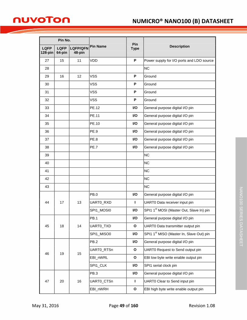
NUMICRO® NANO100 (B) DATASHEET
May 31, 2016 Page 49 of 160 Revision 1.08
NA
NO
10
0 S
ER
IES
DA
TA
SH
EE
T
Pin No.
Pin Name Pin
Type Description
LQFP 128-pin
LQFP 64-pin
LQFP/QFN 48-pin
27 15 11 VDD P Power supply for I/O ports and LDO source
28 NC
29 16 12 VSS P Ground
30 VSS P Ground
31 VSS P Ground
32 VSS P Ground
33 PE.12 I/O General purpose digital I/O pin
34 PE.11 I/O General purpose digital I/O pin
35 PE.10 I/O General purpose digital I/O pin
36 PE.9 I/O General purpose digital I/O pin
37 PE.8 I/O General purpose digital I/O pin
38 PE.7 I/O General purpose digital I/O pin
39 NC
40 NC
41 NC
42 NC
43 NC
44 17 13
PB.0 I/O General purpose digital I/O pin
UART0_RXD I UART0 Data receiver input pin
SPI1_MOSI0 I/O SPI1 1st MOSI (Master Out, Slave In) pin
45 18 14
PB.1 I/O General purpose digital I/O pin
UART0_TXD O UART0 Data transmitter output pin
SPI1_MISO0 I/O SPI1 1st MISO (Master In, Slave Out) pin
46 19 15
PB.2 I/O General purpose digital I/O pin
UART0_RTSn O UART0 Request to Send output pin
EBI_nWRL O EBI low byte write enable output pin
SPI1_CLK I/O SPI1 serial clock pin
47 20 16
PB.3 I/O General purpose digital I/O pin
UART0_CTSn I UART0 Clear to Send input pin
EBI_nWRH O EBI high byte write enable output pin

NUMICRO® NANO100 (B) DATASHEET
May 31, 2016 Page 50 of 160 Revision 1.08
NA
NO
10
0 S
ER
IES
DA
TA
SH
EE
T
Pin No.
Pin Name Pin
Type Description
LQFP 128-pin
LQFP 64-pin
LQFP/QFN 48-pin
SPI1_SS0 I/O SPI1 1st slave select pin
48 21 PD.6 I/O General purpose digital I/O pin
49 22 PD.7 I/O General purpose digital I/O pin
50 23 PD.14 I/O General purpose digital I/O pin
51 24 PD.15 I/O General purpose digital I/O pin
52 PC.5 I/O General purpose digital I/O pin
SPI0_MOSI1 I/O SPI0 2nd
MOSI (Master Out, Slave In) pin
53 PC.4 I/O General purpose digital I/O pin
SPI0_MISO1 I/O SPI0 2nd
MISO (Master In, Slave Out) pin
54 25 17
PC.3 I/O General purpose digital I/O pin
SPI0_MOSI0 I/O SPI0 1st MOSI (Master Out, Slave In) pin
I2S_DO O I2S data output
SC1_RST O SmartCard1 RST pin
55 26 18
PC.2 I/O General purpose digital I/O pin
SPI0_MISO0 I/O SPI0 1st MISO (Master In, Slave Out) pin
I2S_DI I I2S data input
SC1_PWR O SmartCard1 PWR pin
56 27 19
PC.1 I/O General purpose digital I/O pin
SPI0_CLK I/O SPI0 serial clock pin
I2S_BCLK I/O I2S bit clock pin
SC1_DAT I/O SmartCard1 DATA pin(SC1_UART_RXD)
57 28 20
PC.0 / MCLKO I/O General purpose digital I/O pin / Module clock output pin
SPI0_SS0 I/O SPI0 1st slave select pin
I2S_LRCLK I/O I2S left right channel clock
SC1_CLK O SmartCard1 clock pin(SC1_UART_TXD)
58 PE.6 I/O General purpose digital I/O pin
59 NC
60 NC
61 29 21 PE.5 I/O General purpose digital I/O pin
PWM1_CH1 I/O PWM1 Channel1 output

NUMICRO® NANO100 (B) DATASHEET
May 31, 2016 Page 51 of 160 Revision 1.08
NA
NO
10
0 S
ER
IES
DA
TA
SH
EE
T
Pin No.
Pin Name Pin
Type Description
LQFP 128-pin
LQFP 64-pin
LQFP/QFN 48-pin
62 30 22
PB.11 I/O General purpose digital I/O pin
PWM1_CH0 I/O PWM1 Channel0 output
TM3 O Timer3 external counter input
SC2_DAT I/O SmartCard2 DATA pin(SC2_UART_RXD)
SPI0_MISO0 I/O SPI0 1st MISO (Master In, Slave Out) pin
63 31 23
PB.10 I/O General purpose digital I/O pin
SPI0_SS1 I/O SPI0 2nd
slave select pin
TM2 O Timer2 external counter input
SC2_CLK O SmartCard2 clock pin(SC2_UART_TXD)
SPI0_MOSI0 I/O SPI0 1st MOSI (Master Out, Slave In) pin
64 32 24
PB.9 I/O General purpose digital I/O pin
SPI1_SS1 I/O SPI1 2nd
slave select pin
TM1 O Timer1 external counter input
SC2_RST O SmartCard2 RST pin
INT0 I External interrupt0 input pin
65 PE.4 I/O General purpose digital I/O pin
SPI0_MOSI0 I/O SPI0 1st MOSI (Master Out, Slave In) pin
66 PE.3 I/O General purpose digital I/O pin
SPI0_MISO0 I/O SPI0 1st MISO (Master In, Slave Out) pin
67 PE.2 I/O General purpose digital I/O pin
SPI0_CLK I/O SPI0 serial clock pin
68
PE.1 I/O General purpose digital I/O pin.
PWM1_CH3 I/O PWM1 Channel3 output
SPI0_SS0 I/O SPI0 1st slave select pin
69
PE.0 I/O General purpose digital I/O pin
PWM1_CH2 I/O PWM1 Channel2 output
I2S_MCLK O I2S master clock output pin
70
PC.13 I/O General purpose digital I/O pin
SPI1_MOSI1 I/O SPI1 2nd
MOSI (Master Out, Slave In) pin
PWM1_CH1 O PWM1 Channel1 output

NUMICRO® NANO100 (B) DATASHEET
May 31, 2016 Page 52 of 160 Revision 1.08
NA
NO
10
0 S
ER
IES
DA
TA
SH
EE
T
Pin No.
Pin Name Pin
Type Description
LQFP 128-pin
LQFP 64-pin
LQFP/QFN 48-pin
SNOOPER I Snooper pin
INT1 I External interrupt 1
I2C0_SCL O I2C0 clock pin
71
PC.12 I/O General purpose digital I/O pin
SPI1_MISO1 I/O SPI1 2nd
MISO (Master In, Slave Out) pin
PWM1_CH0 O PWM1 Channel0 output
INT0 I External interrupt0 input pin
I2C0_SDA I/O I2C0 data I/O pin
72 33
PC.11 I/O General purpose digital I/O pin
SPI1_MOSI0 I/O SPI1 1st MOSI (Master Out, Slave In) pin
UART1_TXD O UART1 Data transmitter output pin
73 34
PC.10 I/O General purpose digital I/O pin
SPI1_MISO0 I/O SPI1 1st MISO (Master In, Slave Out) pin
UART1_RXD I UART1 Data receiver input pin
74 35
PC.9 I/O General purpose digital I/O pin
SPI1_CLK I/O SPI1 serial clock pin
I2C1_SCL I/O I2C1 clock pin
75 36
PC.8 I/O General purpose digital I/O pin
SPI1_SS0 I/O SPI1 1st slave select pin
EBI_MCLK O EBI external clock output pin
I2C1_SDA I/O I2C1 data I/O pin
76 37 25
PA.15 I/O General purpose digital I/O pin
PWM0_CH3 I/O PWM0 Channel3 output
I2S_MCLK O I2S master clock output pin
TC3 I Timer3 capture input
SC0_PWR O SmartCard0 Power pin
UART0_TXD O UART0 Data transmitter output pin
77 38 26
PA.14 I/O General purpose digital I/O pin
PWM0_CH2 I/O PWM0 Channel2 output
EBI_AD15 I/O EBI Address/Data bus bit15

NUMICRO® NANO100 (B) DATASHEET
May 31, 2016 Page 53 of 160 Revision 1.08
NA
NO
10
0 S
ER
IES
DA
TA
SH
EE
T
Pin No.
Pin Name Pin
Type Description
LQFP 128-pin
LQFP 64-pin
LQFP/QFN 48-pin
TC2 I Timer2 capture input
UART0_RXD I UART0 Data receiver input pin
78 39 27
PA.13 I/O General purpose digital I/O pin
PWM0_CH1 I/O PWM0 Channel1 output
EBI_AD14 I/O EBI Address/Data bus bit14
TC1 I Timer1 capture input
I2C0_SCL I/O I2C0 clock pin
79 40 28
PA.12 I/O General purpose digital I/O pin
PWM0_CH0 I/O PWM0 Channel0 output
EBI_AD13 I/O EBI Address/Data bus bit13
TC0 I Timer0 capture input
I2C0_SDA I/O I2C0 data I/O pin
80 41 29
ICE_DAT I/O Serial Wired Debugger Data pin
PF.0 I/O General purpose digital I/O pin
INT0 I External interrupt0 input pin
81 42 30
ICE_CLK I Serial Wired Debugger Clock pin
PF.1 I/O General purpose digital I/O pin
FCLKO O Frequency Divider output pin
INT1 I External interrupt1 input pin
82 NC
83 VDD P Power supply for I/O ports and LDO source for internal PLL and digital circuit
84 NC
85 VSS P Ground
86 VSS P Ground
87 43 31 AVSS AP Ground Pin for analog circuit
88 AVSS AP Ground Pin for analog circuit
89 44 32
PA.0 I/O General purpose digital I/O pin
AD0 AI ADC analog input0
SC2_CD I SmartCard2 card detect
90 45 33 PA.1 I/O General purpose digital I/O pin

NUMICRO® NANO100 (B) DATASHEET
May 31, 2016 Page 54 of 160 Revision 1.08
NA
NO
10
0 S
ER
IES
DA
TA
SH
EE
T
Pin No.
Pin Name Pin
Type Description
LQFP 128-pin
LQFP 64-pin
LQFP/QFN 48-pin
AD1 AI ADC analog input1
EBI_AD12 I/O EBI Address/Data bus bit12
91 46 34
PA.2 I/O General purpose digital I/O pin
AD2 AI ADC analog input2
EBI_AD11 I/O EBI Address/Data bus bit11
UART1_RXD I UART1 Data receiver input pin
92 47 35
PA.3 I/O General purpose digital I/O pin
AD3 AI ADC analog input3
EBI_AD10 I/O EBI Address/Data bus bit10
UART1_TXD O UART1 Data transmitter output pin
93 48 36
PA.4 I/O General purpose digital I/O pin
AD4 AI ADC analog input4
EBI_AD9 I/O EBI Address/Data bus bit9
SC2_PWR O SmartCard2 Power pin
I2C0_SDA I/O I2C0 data I/O pin
94 49 37
PA.5 I/O General purpose digital I/O pin
AD5 AI ADC analog input5
EBI_AD8 I/O EBI Address/Data bus bit8
SC2_RST O SmartCard2 RST pin
I2C0_SCL I/O I2C0 clock pin
95 50 38
PA.6 I/O General purpose digital I/O pin
AD6 AI ADC analog input6
EBI_AD7 I/O EBI Address/Data bus bit7
TC3 I Timer3 capture input
SC2_CLK O SmartCard2 clock pin(SC2_UART_TXD)
PWM0_CH3 O PWM0 Channel3 output
96
PA.7 I/O General purpose digital I/O pin
AD7 AI ADC analog input7
EBI_AD6 I/O EBI Address/Data bus bit6
TC2 I Timer2 capture input

NUMICRO® NANO100 (B) DATASHEET
May 31, 2016 Page 55 of 160 Revision 1.08
NA
NO
10
0 S
ER
IES
DA
TA
SH
EE
T
Pin No.
Pin Name Pin
Type Description
LQFP 128-pin
LQFP 64-pin
LQFP/QFN 48-pin
SC2_DAT I/O SmartCard2 DATA pin(SC2_UART_RXD)
PWM0_CH2 O PWM0 Channel2 output
97 51 39 VREF AP Voltage reference input for ADC
98 NC
99 52 40 AVDD AP Power supply for internal analog circuit
100
PD.0 I/O General purpose digital I/O pin
UART1_RXD I UART1 Data receiver input pin
SPI2_SS0 I/O SPI2 1st slave select pin
SC1_CLK O SmartCard1 clock pin(SC1_UART_TXD)
AD8 AI ADC analog input8
101
PD.1 I/O General purpose digital I/O pin
UART1_TXD O UART1 Data transmitter output pin
SPI2_CLK I/O SPI2 serial clock pin
SC1_DAT I/O SmartCard1 DATA pin(SC1_UART_RXD).
AD9 AI ADC analog input9
102
PD.2 I/O General purpose digital I/O pin
UART1_RTSn O UART1 Request to Send output pin
I2S_LRCLK I/O I2S left right channel clock
SPI2_MISO0 I/O SPI2 1st MISO (Master In, Slave Out) pin
SC1_PWR O SmartCard1 Power pin
AD10 AI ADC analog input10
103
PD.3 I/O General purpose digital I/O pin
UART1_CTSn I UART1 Clear to Send input pin
I2S_BCLK I/O I2S bit clock pin
SPI2_MOSI0 I/O SPI2 1st MOSI (Master Out, Slave In) pin
SC1_RST O SmartCard1 RST pin
AD11 AI ADC analog input11
104 NC
105 PD.4 I/O General purpose digital I/O pin
I2S_DI I I2S data input

NUMICRO® NANO100 (B) DATASHEET
May 31, 2016 Page 56 of 160 Revision 1.08
NA
NO
10
0 S
ER
IES
DA
TA
SH
EE
T
Pin No.
Pin Name Pin
Type Description
LQFP 128-pin
LQFP 64-pin
LQFP/QFN 48-pin
SPI2_MISO1 I/O SPI2 2nd
MISO (Master In, Slave Out) pin
SC1_CD I SmartCard1 card detect
106
PD.5 I/O General purpose digital I/O pin
I2S_DO O I2S data output
SPI2_MOSI1 I/O SPI2 2nd
MOSI (Master Out, Slave In) pin
107 53 41
PC.7 I/O General purpose digital I/O pin
DA1_OUT AO DAC 1 output
EBI_AD5 I/O EBI Address/Data bus bit5
TC1 I Timer1 capture input
PWM0_CH1 O PWM1 Channel1 output
108 54 42
PC.6 I/O General purpose digital I/O pin
DA0_OUT I DAC0 output
EBI_AD4 I/O EBI Address/Data bus bit4
TC0 I Timer0 capture input
SC1_CD I SmartCard1 card detect pin
PWM0_CH0 O PWM0 Channel0 output
109 55
PC.15 I/O General purpose digital I/O pin
EBI_AD3 I/O EBI Address/Data bus bit3
TC0 I Timer0 capture input
PWM1_CH2 O PWM1 Channel1 output
110 56
PC.14 I/O General purpose digital I/O pin
EBI_AD2 I/O EBI Address/Data bus bit2
PWM1_CH3 I/O PWM1 Channel3 output
111 57 43
PB.15 I/O General purpose digital I/O pin
INT1 I External interrupt1 input pin
SNOOPER I Snooper pin
SC1_CD I SmartCard1 card detect
112 NC
113 58 44 XT1_IN O External 4~24 MHz crystal output pin
PF.3 I/O General purpose digital I/O pin
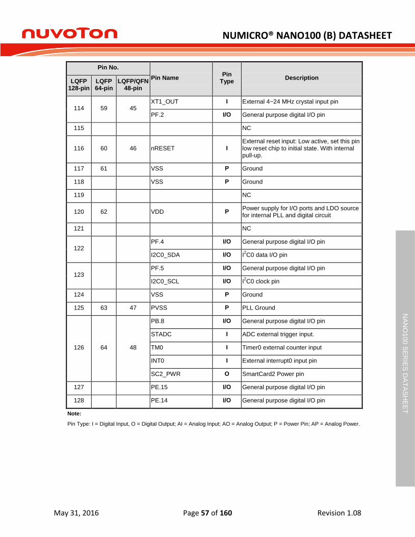
NUMICRO® NANO100 (B) DATASHEET
May 31, 2016 Page 57 of 160 Revision 1.08
NA
NO
10
0 S
ER
IES
DA
TA
SH
EE
T
Pin No.
Pin Name Pin
Type Description
LQFP 128-pin
LQFP 64-pin
LQFP/QFN 48-pin
114 59 45 XT1_OUT I External 4~24 MHz crystal input pin
PF.2 I/O General purpose digital I/O pin
115 NC
116 60 46 nRESET I External reset input: Low active, set this pin low reset chip to initial state. With internal pull-up.
117 61 VSS P Ground
118 VSS P Ground
119 NC
120 62 VDD P Power supply for I/O ports and LDO source for internal PLL and digital circuit
121 NC
122 PF.4 I/O General purpose digital I/O pin
I2C0_SDA I/O I2C0 data I/O pin
123 PF.5 I/O General purpose digital I/O pin
I2C0_SCL I/O I2C0 clock pin
124 VSS P Ground
125 63 47 PVSS P PLL Ground
126 64 48
PB.8 I/O General purpose digital I/O pin
STADC I ADC external trigger input.
TM0 I Timer0 external counter input
INT0 I External interrupt0 input pin
SC2_PWR O SmartCard2 Power pin
127 PE.15 I/O General purpose digital I/O pin
128 PE.14 I/O General purpose digital I/O pin
Note:
Pin Type: I = Digital Input, O = Digital Output; AI = Analog Input; AO = Analog Output; P = Power Pin; AP = Analog Power.

NUMICRO® NANO100 (B) DATASHEET
May 31, 2016 Page 58 of 160 Revision 1.08
NA
NO
10
0 S
ER
IES
DA
TA
SH
EE
T
3.4.2 NuMicro® Nano110 Pin Description
Pin No.
Pin Name Pin Type Description LQFP
128-pin LQFP 64-pin
LQFP 48-pin
1 PE.13 I/O General purpose digital I/O pin
LCD_SEG27 O LCD segment output 27 at LQFP128
2 1
PB.14 I/O General purpose digital I/O pin
INT0 I External interrupt0 input pin
SC2_CD I SmartCard2 card detect
SPI2_SS1 I/O SPI2 2nd
slave select pin
LCD_SEG12 O LCD segment output 12 at LQFP64
LCD_SEG26 O LCD segment output 26 at LQFP128
3 2
PB.13 I/O General purpose digital I/O pin
EBI_AD1 I/O EBI Address/Data bus bit1
LCD_SEG11 O LCD segment output 11 at LQFP64
LCD_SEG25 O LCD segment output 25 at LQFP128
4 3
PB.12 I/O General purpose digital I/O pin
EBI_AD0 I/O EBI Address/Data bus bit0
FCLKO O Frequency Divider output pin
LCD_SEG10 O LCD segment output 10 at LQFP64
LCD_SEG24 O LCD segment output 24 at LQFP128
5 NC
6 4 X32O O External 32.768 kHz crystal output pin
7 5 X32I I External 32.768 kHz crystal input pin
8 NC
9 6
PA.11 I/O General purpose digital I/O pin
I2C1_SCL I/O I2C1 clock pin
EBI_nRD O EBI read enable output pin
SC0_RST O SmartCard0 RST pin
SPI2_MOSI0 I/O SPI2 1st MOSI (Master Out, Slave In) pin
LCD_SEG9 O LCD segment output 9 at LQFP64
LCD_SEG23 O LCD segment output 23 at LQFP128
10 7 PA.10 I/O General purpose digital I/O pin
I2C1_SDA I/O I2C1 data I/O pin
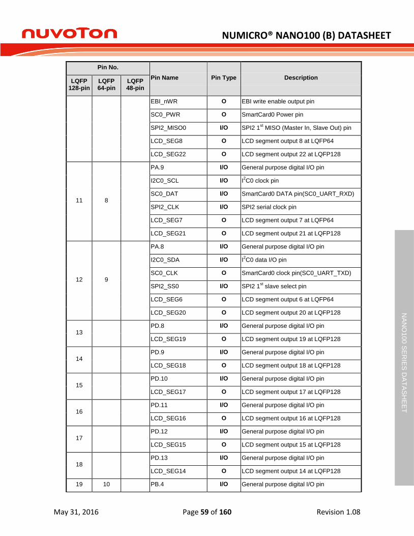
NUMICRO® NANO100 (B) DATASHEET
May 31, 2016 Page 59 of 160 Revision 1.08
NA
NO
10
0 S
ER
IES
DA
TA
SH
EE
T
Pin No.
Pin Name Pin Type Description LQFP
128-pin LQFP 64-pin
LQFP 48-pin
EBI_nWR O EBI write enable output pin
SC0_PWR O SmartCard0 Power pin
SPI2_MISO0 I/O SPI2 1st MISO (Master In, Slave Out) pin
LCD_SEG8 O LCD segment output 8 at LQFP64
LCD_SEG22 O LCD segment output 22 at LQFP128
11 8
PA.9 I/O General purpose digital I/O pin
I2C0_SCL I/O I2C0 clock pin
SC0_DAT I/O SmartCard0 DATA pin(SC0_UART_RXD)
SPI2_CLK I/O SPI2 serial clock pin
LCD_SEG7 O LCD segment output 7 at LQFP64
LCD_SEG21 O LCD segment output 21 at LQFP128
12 9
PA.8 I/O General purpose digital I/O pin
I2C0_SDA I/O I2C0 data I/O pin
SC0_CLK O SmartCard0 clock pin(SC0_UART_TXD)
SPI2_SS0 I/O SPI2 1st slave select pin
LCD_SEG6 O LCD segment output 6 at LQFP64
LCD_SEG20 O LCD segment output 20 at LQFP128
13 PD.8 I/O General purpose digital I/O pin
LCD_SEG19 O LCD segment output 19 at LQFP128
14 PD.9 I/O General purpose digital I/O pin
LCD_SEG18 O LCD segment output 18 at LQFP128
15 PD.10 I/O General purpose digital I/O pin
LCD_SEG17 O LCD segment output 17 at LQFP128
16 PD.11 I/O General purpose digital I/O pin
LCD_SEG16 O LCD segment output 16 at LQFP128
17 PD.12 I/O General purpose digital I/O pin
LCD_SEG15 O LCD segment output 15 at LQFP128
18 PD.13 I/O General purpose digital I/O pin
LCD_SEG14 O LCD segment output 14 at LQFP128
19 10 PB.4 I/O General purpose digital I/O pin

NUMICRO® NANO100 (B) DATASHEET
May 31, 2016 Page 60 of 160 Revision 1.08
NA
NO
10
0 S
ER
IES
DA
TA
SH
EE
T
Pin No.
Pin Name Pin Type Description LQFP
128-pin LQFP 64-pin
LQFP 48-pin
UART1_RXD I UART1 Data receiver input pin
SC0_CD I SmartCard0 card detect pin
SPI2_SS0 I/O SPI2 1st slave select pin
LCD_SEG5 O LCD segment output 5 at LQFP64
LCD_SEG13 O LCD segment output 13 at LQFP128
20 11
PB.5 I/O General purpose digital I/O pin
UART1_TXD O UART1 Data transmitter output pin
SC0_RST O SmartCard0 RST pin
SPI2_CLK I/O SPI2 serial clock pin
LCD_SEG4 O LCD segment output 4 at LQFP64
LCD_SEG12 O LCD segment output 12 at LQFP128
21 12
PB.6 I/O General purpose digital I/O pin
UART1_RTSn O UART1 Request to Send output pin
EBI_ALE O EBI address latch enable output pin
SPI2_MISO0 I/O SPI2 1st MISO (Master In, Slave Out) pin
LCD_SEG3 O LCD segment output 3 at LQFP64
LCD_SEG11 O LCD segment output 11 at LQFP128
22 13
PB.7 I/O General purpose digital I/O pin
UART1_CTSn I UART1 Clear to Send input pin
EBI_nCS O EBI chip select enable output pin
SPI2_MOSI0 I/O SPI2 1st MOSI (Master Out, Slave In) pin
LCD_SEG2 O LCD segment output 2 at LQFP64
LCD_SEG10 O LCD segment output 10 at LQFP128
23 NC
24 14 LDO_CAP P LDO output pin
25 NC
26 NC
27 15 VDD P Power supply for I/O ports and LDO source
28 NC
29 16 VSS P Ground

NUMICRO® NANO100 (B) DATASHEET
May 31, 2016 Page 61 of 160 Revision 1.08
NA
NO
10
0 S
ER
IES
DA
TA
SH
EE
T
Pin No.
Pin Name Pin Type Description LQFP
128-pin LQFP 64-pin
LQFP 48-pin
30 VSS P Ground
31 VSS P Ground
32 VSS P Ground
33 PE.12 I/O General purpose digital I/O pin
UART1_CTSn I UART1 Clear to Send input pin
34 PE.11 I/O General purpose digital I/O pin
UART1_RTSn O UART1 Request to Send output pin
35 PE.10 I/O General purpose digital I/O pin
UART1_TXD O UART1 Data transmitter output pin
36 PE.9 I/O General purpose digital I/O pin
UART1_RXD I UART1 Data receiver input pin
37 PE.8 I/O General purpose digital I/O pin
LCD_SEG9 O LCD segment output 9 at LQFP128
38 PE.7 I/O General purpose digital I/O pin
LCD_SEG8 O LCD segment output 8 at LQFP128
39 NC
40 NC
41 NC
42 NC
43 NC
44 17
PB.0 I/O General purpose digital I/O pin
UART0_RXD I UART0 Data receiver input pin
SPI1_MOSI0 I/O SPI1 1st MOSI (Master Out, Slave In) pin
LCD_SEG1 O LCD segment output 1 at LQFP64 (or as LD_COM5)
LCD_SEG7 O LCD segment output 7 at LQFP128
45 18
PB.1 I/O General purpose digital I/O pin
UART0_TXD O UART0 Data transmitter output pin
SPI1_MISO0 I/O SPI1 1st MISO (Master In, Slave Out) pin
LCD_SEG0 O LCD segment output 0 at LQFP64 (or as LCD_COM4)

NUMICRO® NANO100 (B) DATASHEET
May 31, 2016 Page 62 of 160 Revision 1.08
NA
NO
10
0 S
ER
IES
DA
TA
SH
EE
T
Pin No.
Pin Name Pin Type Description LQFP
128-pin LQFP 64-pin
LQFP 48-pin
LCD_SEG6 O LCD segment output 6 at LQFP128
46 19
PB.2 I/O General purpose digital I/O pin
UART0_RTSn O UART0 Request to Send output pin
EBI_nWRL O EBI low byte write enable output pin
SPI1_CLK I/O SPI1 serial clock pin
LCD_COM3 O LCD common output 3 at LQFP64
LCD_SEG5 O LCD segment output 5 at LQFP128
47 20
PB.3 I/O General purpose digital I/O pin
UART0_CTSn I UART0 Clear to Send input pin
EBI_nWRH O EBI high byte write enable output pin
SPI1_SS0 I/O SPI1 1st slave select pin
LCD_COM2 O LCD common output 2 at LQFP64
LCD_SEG4 O LCD segment output 4 at LQFP128
48 21 PD.6 I/O General purpose digital I/O pin
LCD_SEG3 O LCD segment output 3 at LQFP128
49 22 PD.7 I/O General purpose digital I/O pin
LCD_SEG2 O LCD segment output 2 at LQFP128
50 23
PD.14 I/O General purpose digital I/O pin
LCD_SEG1 O LCD segment output 1 at LQFP128 (or as LCD_COM5)
51 24
PD.15 I/O General purpose digital I/O pin
LCD_SEG0 O LCD segment output 0 at LQFP128 (or as LCD_COM4)
52
PC.5 I/O General purpose digital I/O pin
SPI0_MOSI1 I/O SPI0 2nd
MOSI (Master Out, Slave In) pin
LCD_COM3 O LCD common output 3 at LQFP128
53
PC.4 I/O General purpose digital I/O pin
SPI0_MISO1 I/O SPI0 2nd
MISO (Master In, Slave Out) pin
LCD_COM2 O LCD common output 2 at LQFP128
54 25 PC.3 I/O General purpose digital I/O pin
SPI0_MOSI0 I/O SPI0 1st MOSI (Master Out, Slave In) pin

NUMICRO® NANO100 (B) DATASHEET
May 31, 2016 Page 63 of 160 Revision 1.08
NA
NO
10
0 S
ER
IES
DA
TA
SH
EE
T
Pin No.
Pin Name Pin Type Description LQFP
128-pin LQFP 64-pin
LQFP 48-pin
I2S_DO O I2S data output
SC1_RST O SmartCard1 RST pin
LCD_COM1 O LCD common output 1 at LQFP64
LCD_COM1 O LCD common output 1 at LQFP128
55 26
PC.2 I/O General purpose digital I/O pin
SPI0_MISO0 I/O SPI0 1st MISO (Master In, Slave Out) pin
I2S_DI I I2S data input
SC1_PWR O SmartCard1 PWR pin
LCD_COM0 O LCD common output 0 at LQFP64
LCD_COM0 O LCD common output 0 at LQFP128
56 27
PC.1 I/O General purpose digital I/O pin
SPI0_CLK I/O SPI0 serial clock pin
I2S_BCLK I/O I2S bit clock pin
SC1_DAT I/O SmartCard1 DATA pin(SC1_UART_RXD)
LCD_DH2 O LCD externl capacitor pin of charge pump circuit at LQFP64
LCD_DH2 O LCD externl capacitor pin of charge pump circuit at LQFP128
57 28
PC.0 / MCLKO I/O General purpose digital I/O pin / Module clock output pin
SPI0_SS0 I/O SPI0 1st slave select pin
I2S_LRCLK I/O I2S left right channel clock
SC1_CLK O SmartCard1 clock pin(SC1_UART_TXD)
LCD_DH1 O LCD externl capacitor pin of charge pump circuit at LQFP64
LCD_DH1 O LCD externl capacitor pin of charge pump circuit at LQFP128
58 PE.6 I/O General purpose digital I/O pin
59 29 LCD_VLCD AO LCD power supply pin
60 NC
61 PE.5 I/O General purpose digital I/O pin
62 30 PB.11 I/O General purpose digital I/O pin
PWM1_CH0 I/O PWM1 Channel0 output

NUMICRO® NANO100 (B) DATASHEET
May 31, 2016 Page 64 of 160 Revision 1.08
NA
NO
10
0 S
ER
IES
DA
TA
SH
EE
T
Pin No.
Pin Name Pin Type Description LQFP
128-pin LQFP 64-pin
LQFP 48-pin
TM3 O Timer3 external counter input
SC2_DAT I/O SmartCard2 DATA pin(SC2_UART_RXD)
SPI0_MISO0 I/O SPI0 1st MISO (Master In, Slave Out) pin
LCD_V1 O Unit voltage for LCD charge pump circuit at LQFP64
LCD_V1 O LCD Unit voltage for LCD charge pump circuit at LQFP128
63 31
PB.10 I/O General purpose digital I/O pin
SPI0_SS1 I/O SPI0 2nd
slave select pin
TM2 O Timer2 external counter input
SC2_CLK O SmartCard2 clock pin(SC2_UART_TXD)
SPI0_MOSI0 I/O SPI0 1st MOSI (Master Out, Slave In) pin
LCD_V2 O LCD driver biasing voltage at LQFP64
LCD_V2 O LCD driver biasing voltage at LQFP128
64 32
PB.9 I/O General purpose digital I/O pin
SPI1_SS1 I/O SPI1 2nd
slave select pin
TM1 O Timer1 external counter input
SC2_RST O SmartCard2 RST pin
INT0 I External interrupt0 input pin
LCD_V3 O LCD driver biasing voltage at LQFP64
LCD_V3 O LCD driver biasing voltage at LQFP128
65 PE.4 I/O General purpose digital I/O pin
SPI0_MOSI0 I/O SPI0 1st MOSI (Master Out, Slave In) pin
66 PE.3 I/O General purpose digital I/O pin
SPI0_MISO0 I/O SPI0 1st MISO (Master In, Slave Out) pin
67 PE.2 I/O General purpose digital I/O pin
SPI0_CLK I/O SPI0 serial clock pin
68
PE.1 I/O General purpose digital I/O pin
PWM1_CH3 I/O PWM1 Channel3 output
SPI0_SS0 I/O SPI0 1st slave select pin
69 PE.0 I/O General purpose digital I/O pin

NUMICRO® NANO100 (B) DATASHEET
May 31, 2016 Page 65 of 160 Revision 1.08
NA
NO
10
0 S
ER
IES
DA
TA
SH
EE
T
Pin No.
Pin Name Pin Type Description LQFP
128-pin LQFP 64-pin
LQFP 48-pin
PWM1_CH2 I/O PWM1 Channel2 output
I2S_MCLK O I2S master clock output pin
70
PC.13 I/O General purpose digital I/O pin
SPI1_MOSI1 I/O SPI1 2nd
MOSI (Master Out, Slave In) pin
PWM1_CH1 O PWM1 Channel1 output
SNOOPER I Snooper pin
INT1 I External interrupt 1
I2C0_SCL O I2C0 clock pin
71
PC.12 I/O General purpose digital I/O pin
SPI1_MISO1 I/O SPI1 2nd
MISO (Master In, Slave Out) pin
PWM1_CH0 O PWM1 Channel0 output
INT0 I External interrupt0 input pin
I2C0_SDA I/O I2C0 data I/O pin
72 33
PC.11 I/O General purpose digital I/O pin
SPI1_MOSI0 I/O SPI1 1st MOSI (Master Out, Slave In) pin
UART1_TXD O UART1 Data transmitter output pin
LCD_SEG31 O LCD segment output 31 at LQFP64
73 34
PC.10 I/O General purpose digital I/O pin
SPI1_MISO0 I/O SPI1 1st MISO (Master In, Slave Out) pin
UART1_RXD I UART1 Data receiver input pin
LCD_SEG30 O LCD segment output 30 at LQFP64
74 35
PC.9 I/O General purpose digital I/O pin
SPI1_CLK I/O SPI1 serial clock pin
I2C1_SCL I/O I2C1 clock pin
LCD_SEG29 O LCD segment output 29 at LQFP64
75 36
PC.8 I/O General purpose digital I/O pin
SPI1_SS0 I/O SPI1 1st slave select pin
EBI_MCLK O EBI external clock output pin
I2C1_SDA I/O I2C1 data I/O pin
LCD_SEG28 O LCD segment output 28 at LQFP64

NUMICRO® NANO100 (B) DATASHEET
May 31, 2016 Page 66 of 160 Revision 1.08
NA
NO
10
0 S
ER
IES
DA
TA
SH
EE
T
Pin No.
Pin Name Pin Type Description LQFP
128-pin LQFP 64-pin
LQFP 48-pin
76 37
PA.15 I/O General purpose digital I/O pin
PWM0_CH3 I/O PWM0 Channel3 output
I2S_MCLK O I2S master clock output pin
TC3 I Timer3 capture input
SC0_PWR O SmartCard0 Power pin
UART0_TXD O UART0 Data transmitter output pin
LCD_SEG27 O LCD segment output 27 at LQFP64
77 38
PA.14 I/O General purpose digital I/O pin
PWM0_CH2 I/O PWM0 Channel2 output
EBI_AD15 I/O EBI Address/Data bus bit15
TC2 I Timer2 capture input
UART0_RXD I UART0 Data receiver input pin
LCD_SEG26 O LCD segment output 26 at LQFP64
78 39
PA.13 I/O General purpose digital I/O pin
PWM0_CH1 I/O PWM0 Channel1 output
EBI_AD14 I/O EBI Address/Data bus bit14
TC1 I Timer1 capture input
I2C0_SCL I/O I2C0 clock pin
LCD_SEG25 O LCD segment output 25 at LQFP64
79 40
PA.12 I/O General purpose digital I/O pin
PWM0_CH0 I/O PWM0 Channel0 output
EBI_AD13 I/O EBI Address/Data bus bit13
TC0 I Timer0 capture input
I2C0_SDA I/O I2C0 data I/O pin
LCD_SEG24 O LCD segment output 24 at LQFP64
80 41
ICE_DAT I/O Serial Wired Debugger Data pin
PF.0 I/O General purpose digital I/O pin
INT0 I External interrupt0 input pin
81 42 ICE_CLK I Serial Wired Debugger Clock pin
PF.1 I/O General purpose digital I/O pin

NUMICRO® NANO100 (B) DATASHEET
May 31, 2016 Page 67 of 160 Revision 1.08
NA
NO
10
0 S
ER
IES
DA
TA
SH
EE
T
Pin No.
Pin Name Pin Type Description LQFP
128-pin LQFP 64-pin
LQFP 48-pin
FCLKO O Frequency Divider output pin
INT1 I External interrupt1 input pin
82 NC
83 VDD P Power supply for I/O ports and LDO source for internal PLL and digital circuit
84 NC
85 VSS P Ground
86 VSS P Ground
87 43 AVSS AP Ground Pin for analog circuit
88 AVSS AP Ground Pin for analog circuit
89 44
PA.0 I/O General purpose digital I/O pin
AD0 AI ADC analog input0
SC2_CD I SmartCard2 card detect
90 45
PA.1 I/O General purpose digital I/O pin
AD1 AI ADC analog input1
EBI_AD12 I/O EBI Address/Data bus bit12
91 46
PA.2 I/O General purpose digital I/O pin
AD2 AI ADC analog input2
EBI_AD11 I/O EBI Address/Data bus bit11
UART1_RXD I UART1 Data receiver input pin
LCD_SEG23* AO LCD segment output 23 at LQFP64
92 47
PA.3 I/O General purpose digital I/O pin
AD3 AI ADC analog input3
EBI_AD10 I/O EBI Address/Data bus bit10
UART1_TXD O UART1 Data transmitter output pin
LCD_SEG22* AO LCD segment output 22 at LQFP64
93 48
PA.4 I/O General purpose digital I/O pin
AD4 AI ADC analog input4
EBI_AD9 I/O EBI Address/Data bus bit9
SC2_PWR O SmartCard2 Power pin
I2C0_SDA I/O I2C0 data I/O pin

NUMICRO® NANO100 (B) DATASHEET
May 31, 2016 Page 68 of 160 Revision 1.08
NA
NO
10
0 S
ER
IES
DA
TA
SH
EE
T
Pin No.
Pin Name Pin Type Description LQFP
128-pin LQFP 64-pin
LQFP 48-pin
LCD_SEG21* AO LCD segment output 21 at LQFP64
LCD_SEG39* AO LCD segment output 39 at LQFP128
94 49
PA.5 I/O General purpose digital I/O pin
AD5 AI ADC analog input5
EBI_AD8 I/O EBI Address/Data bus bit8
SC2_RST O SmartCard2 RST pin
I2C0_SCL I/O I2C0 clock pin
LCD_SEG20* AO LCD segment output 19 at LQFP64
LCD_SEG38* AO LCD segment output 37 at LQFP128
95 50
PA.6 I/O General purpose digital I/O pin
AD6 AI ADC analog input6
EBI_AD7 I/O EBI Address/Data bus bit7
TC3 I Timer3 capture input
SC2_CLK O SmartCard2 clock pin(SC2_UART_TXD)
PWM0_CH3 O PWM0 Channel3 output
LCD_SEG19* AO LCD segment output 19 at LQFP64
LCD_SEG37* AO LCD segment output 37 at LQFP128
96
PA.7 I/O General purpose digital I/O pin
AD7 AI ADC analog input7
EBI_AD6 I/O EBI Address/Data bus bit6
TC2 I Timer2 capture input
SC2_DAT I/O SmartCard2 DATA pin(SC2_UART_RXD)
PWM0_CH2 O PWM0 Channel2 output
LCD_SEG36* AO LCD segment output 36 output at LQFP128
97 51 VREF AP Voltage reference input for ADC
98 NC
99 52 AVDD AP Power supply for internal analog circuit
100
PD.0 I/O General purpose digital I/O pin
UART1_RXD I UART1 Data receiver input pin
SPI2_SS0 I/O SPI2 1st slave select pin

NUMICRO® NANO100 (B) DATASHEET
May 31, 2016 Page 69 of 160 Revision 1.08
NA
NO
10
0 S
ER
IES
DA
TA
SH
EE
T
Pin No.
Pin Name Pin Type Description LQFP
128-pin LQFP 64-pin
LQFP 48-pin
SC1_CLK O SmartCard1 clock pin(SC1_UART_TXD)
AD8 AI ADC analog input8
101
PD.1 I/O General purpose digital I/O pin
UART1_TXD O UART1 Data transmitter output pin
SPI2_CLK I/O SPI2 serial clock pin
SC1_DAT I/O SmartCard1 DATA pin(SC1_UART_RXD)
AD9 AI ADC analog input9
102
PD.2 I/O General purpose digital I/O pin
UART1_RTSn UART1 Request to Send output pin
I2S_LRCLK I/O I2S left right channel clock
SPI2_MISO0 I/O SPI2 1st MISO (Master In, Slave Out) pin
SC1_PWR O SmartCard1 Power pin
AD10 AI ADC analog input10
103
PD.3 I/O General purpose digital I/O pin
UART1_CTSn UART1 Clear to Send input pin
I2S_BCLK I/O I2S bit clock pin
SPI2_MOSI0 I/O SPI2 1st MOSI (Master Out, Slave In) pin
SC1_RST O SmartCard1 RST pin
AD11 AI ADC analog input11
104 NC
105
PD.4 I/O General purpose digital I/O pin
I2S_DI I I2S data input
SPI2_MISO1 I/O SPI2 2nd
MISO (Master In, Slave Out) pin
SC1_CD I SmartCard1 card detect
LCD_SEG35 AO LCD segment output 35 at LQFP10
106
PD.5 I/O General purpose digital I/O pin
I2S_DO O I2S data output
SPI2_MOSI1 I/O SPI2 2nd
MOSI (Master Out, Slave In) pin
LCD_SEG34 AO LCD segment output 34 at LQFP128
107 53 PC.7 I/O General purpose digital I/O pin

NUMICRO® NANO100 (B) DATASHEET
May 31, 2016 Page 70 of 160 Revision 1.08
NA
NO
10
0 S
ER
IES
DA
TA
SH
EE
T
Pin No.
Pin Name Pin Type Description LQFP
128-pin LQFP 64-pin
LQFP 48-pin
DA1_OUT AO DAC 1 output
EBI_AD5 I/O EBI Address/Data bus bit5
TC1 I Timer1 capture input
PWM0_CH1 O PWM1 Channel1 output
LCD_SEG17* AO LCD segment output 17 at LQFP64
108 54
PC.6 I/O General purpose digital I/O pin
DA0_OUT I DAC0 output
EBI_AD4 I/O EBI Address/Data bus bit4
TC0 I Timer0 capture input
SC1_CD I SmartCard1 card detect pin
PWM0_CH0 O PWM0 Channel0 output
109 55
PC.15 I/O General purpose digital I/O pin
EBI_AD3 I/O EBI Address/Data bus bit3
TC0 I Timer0 capture input
PWM1_CH2 O PWM1 Channel1 output
LCD_SEG16 AO LCD segment output 16 at LQFP64
LCD_SEG33 AO LCD segment output 33 at LQFP128
110 56
PC.14 I/O General purpose digital I/O pin
EBI_AD2 I/O EBI Address/Data bus bit2
PWM1_CH3 I/O PWM1 Channel3 output
LCD_SEG15 AO LCD segment output 15 at LQFP64
LCD_SEG32 AO LCD segment output 32 at LQFP128
111 57
PB.15 I/O General purpose digital I/O pin
INT1 I External interrupt1 input pin
SNOOPER I Snooper pin
LCD_SEG14 AO LCD segment output 14 at LQFP64
LCD_SEG31 AO LCD segment output 31 at LQFP128
112 NC
113 58 XT1_IN O External 4~24 MHz crystal output pin
PF.3 I/O General purpose digital I/O pin

NUMICRO® NANO100 (B) DATASHEET
May 31, 2016 Page 71 of 160 Revision 1.08
NA
NO
10
0 S
ER
IES
DA
TA
SH
EE
T
Pin No.
Pin Name Pin Type Description LQFP
128-pin LQFP 64-pin
LQFP 48-pin
114 59 XT1_OUT I External 4~24 MHz crystal input pin
PF.2 I/O General purpose digital I/O pin
115 NC
116 60 nRESET I External reset input: Low active, set this pin low reset chip to initial state. With internal pull-up.
117 61 VSS P Ground
118 VSS P Ground
119 NC
120 62 VDD P Power supply for I/O ports and LDO source for internal PLL and digital circuit
121 NC
122 PF.4 I/O General purpose digital I/O pin
I2C0_SDA I/O I2C0 data I/O pin
123 PF.5 I/O General purpose digital I/O pin
I2C0_SCL I/O I2C0 clock pin
124 VSS P Ground
125 63 PVSS P PLL Ground
126 64
PB.8 I/O General purpose digital I/O pin
STADC I ADC external trigger input.
TM0 I Timer0 external counter input
INT0 I External interrupt0 input pin
SC2_PWR O SmartCard2 Power pin
LCD_SEG13 AO LCD segment output 13 at LQFP64
LCD_SEG30 AO LCD segment output 30 at LQFP128
127 PE.15 I/O General purpose digital I/O pin
LCD_SEG29 O LCD segment output 29 at LQFP128
128 PE.14 I/O General purpose digital I/O pin
LCD_SEG28 O LCD segment output 28 at LQFP128
Note:
1. Pin Type: I = Digital Input, O=Digital Output; AI=Analog Input; AO= Analog Output; P=Power Pin; AP=Analog Power;
2. * : Output voltage for ADC/LCD shared pins cannot be higher than VDD because these pins are without 5V tolerance.
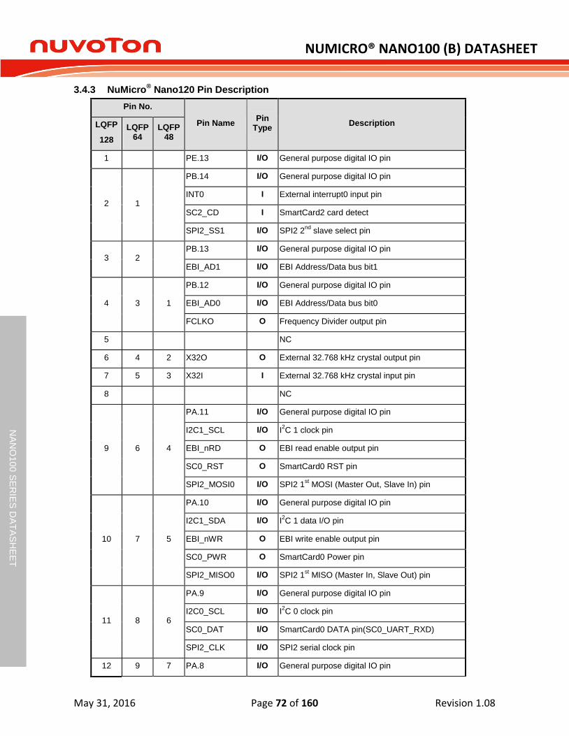
NUMICRO® NANO100 (B) DATASHEET
May 31, 2016 Page 72 of 160 Revision 1.08
NA
NO
10
0 S
ER
IES
DA
TA
SH
EE
T
3.4.3 NuMicro® Nano120 Pin Description
Pin No.
Pin Name Pin
Type Description LQFP
128
LQFP 64
LQFP 48
1 PE.13 I/O General purpose digital IO pin
2 1
PB.14 I/O General purpose digital IO pin
INT0 I External interrupt0 input pin
SC2_CD I SmartCard2 card detect
SPI2_SS1 I/O SPI2 2nd
slave select pin
3 2 PB.13 I/O General purpose digital IO pin
EBI_AD1 I/O EBI Address/Data bus bit1
4 3 1
PB.12 I/O General purpose digital IO pin
EBI_AD0 I/O EBI Address/Data bus bit0
FCLKO O Frequency Divider output pin
5 NC
6 4 2 X32O O External 32.768 kHz crystal output pin
7 5 3 X32I I External 32.768 kHz crystal input pin
8 NC
9 6 4
PA.11 I/O General purpose digital IO pin
I2C1_SCL I/O I2C 1 clock pin
EBI_nRD O EBI read enable output pin
SC0_RST O SmartCard0 RST pin
SPI2_MOSI0 I/O SPI2 1st MOSI (Master Out, Slave In) pin
10 7 5
PA.10 I/O General purpose digital IO pin
I2C1_SDA I/O I2C 1 data I/O pin
EBI_nWR O EBI write enable output pin
SC0_PWR O SmartCard0 Power pin
SPI2_MISO0 I/O SPI2 1st MISO (Master In, Slave Out) pin
11 8 6
PA.9 I/O General purpose digital IO pin
I2C0_SCL I/O I2C 0 clock pin
SC0_DAT I/O SmartCard0 DATA pin(SC0_UART_RXD)
SPI2_CLK I/O SPI2 serial clock pin
12 9 7 PA.8 I/O General purpose digital IO pin

NUMICRO® NANO100 (B) DATASHEET
May 31, 2016 Page 73 of 160 Revision 1.08
NA
NO
10
0 S
ER
IES
DA
TA
SH
EE
T
Pin No.
Pin Name Pin
Type Description LQFP
128
LQFP 64
LQFP 48
I2C0_SDA I/O I2C 0 data I/O pin
SC0_CLK O SmartCard0 clock pin(SC0_UART_TXD)
SPI2_SS0 I/O SPI2 1st slave select pin
13 PD.8 I/O General purpose digital IO pin
14 PD.9 I/O General purpose digital IO pin
15 PD.10 I/O General purpose digital IO pin
16 PD.11 I/O General purpose digital IO pin
17 PD.12 I/O General purpose digital IO pin
18 PD.13 I/O General purpose digital IO pin
19 10 8
PB.4 I/O General purpose digital IO pin
UART1_RXD I UART1 Data receiver input pin
SC0_CD I SmartCard0 card detect pin
SPI2_SS0 I/O SPI2 1st slave select pin
20 11 9
PB.5 I/O General purpose digital IO pin
UART1_TXD O UART1 Data transmitter output pin
SC0_RST O SmartCard0 RST pin
SPI2_CLK I/O SPI2 serial clock pin
21 12
PB.6 I/O General purpose digital IO pin
UART1_nRTS O UART1 Request to Send output pin
EBI_ALE O EBI address latch enable output pin
SPI2_MISO0 I/O SPI2 1st MISO (Master In, Slave Out) pin
22 13
PB.7 I/O General purpose digital IO pin
UART1_nCTS I UART1 Clear to Send input pin
EBI_nCS O EBI chip select enable output pin
SPI2_MOSI0 I/O SPI2 1st MOSI (Master Out, Slave In) pin
23 NC
24 14 10 LDO_CAP P LDO output pin
25 NC
26 NC
27 15 11 VDD P Power supply for I/O ports and LDO source

NUMICRO® NANO100 (B) DATASHEET
May 31, 2016 Page 74 of 160 Revision 1.08
NA
NO
10
0 S
ER
IES
DA
TA
SH
EE
T
Pin No.
Pin Name Pin
Type Description LQFP
128
LQFP 64
LQFP 48
28 NC
29 16 12 VSS P Ground
30 VSS P Ground
31 VSS P Ground
32 VSS P Ground
33 PE.12 I/O General purpose digital IO pin
34 PE.11 I/O General purpose digital IO pin
35 PE.10 I/O General purpose digital IO pin
36 PE.9 I/O General purpose digital IO pin
37 PE.8 I/O General purpose digital IO pin
38 PE.7 I/O General purpose digital IO pin
39 NC
40 17 13 USB_VBUS USB POWER SUPPLY: From USB Host or HUB.
41 18 14 USB_VDD33_CAP
USB Internal Power Regulator Output 3.3V Decoupling Pin
42 19 15 USB_D- USB USB Differential Signal D-
43 20 16 USB_D+ USB USB Differential Signal D+
44 21 17
PB.0 I/O General purpose digital IO pin
UART0_RXD I UART0 Data receiver input pin
SPI1_MOSI0 I/O SPI1 1st MOSI (Master Out, Slave In) pin
45 22 18
PB.1 I/O General purpose digital IO pin
UART0_TXD O UART0 Data transmitter output pin
SPI1_MISO0 I/O SPI1 1st MISO (Master In, Slave Out) pin
46 23 19
PB.2 I/O General purpose digital IO pin
UART0_nRTS O UART0 Request to Send output pin
EBI_nWRL O EBI low byte write enable output pin
SPI1_CLK I/O SPI1 serial clock pin
47 24 20
PB.3 I/O General purpose digital IO pin
UART0_nCTS I UART0 Clear to Send input pin
EBI_nWRH O EBI high byte write enable output pin
SPI1_SS0 I/O SPI1 1st slave select pin

NUMICRO® NANO100 (B) DATASHEET
May 31, 2016 Page 75 of 160 Revision 1.08
NA
NO
10
0 S
ER
IES
DA
TA
SH
EE
T
Pin No.
Pin Name Pin
Type Description LQFP
128
LQFP 64
LQFP 48
48 PD.6 I/O General purpose digital IO pin
49 PD.7 I/O General purpose digital IO pin
50 PD.14 I/O General purpose digital IO pin
51 PD.15 I/O General purpose digital IO pin
52 PC.5 I/O General purpose digital IO pin
SPI0_MOSI1 I/O SPI0 2nd
MOSI (Master Out, Slave In) pin
53 PC.4 I/O General purpose digital IO pin
SPI0_MISO1 I/O SPI0 2nd
MISO (Master In, Slave Out) pin
54 25 21
PC.3 I/O General purpose digital IO pin
SPI0_MOSI0 I/O SPI0 1st MOSI (Master Out, Slave In) pin
I2S_DO O I2S data output
SC1_RST O SmartCard1 RST pin
55 26 22
PC.2 I/O General purpose digital IO pin
SPI0_MISO0 I/O SPI0 1st MISO (Master In, Slave Out) pin
I2S_DI I I2S data input
SC1_PWR O SmartCard1 PWR pin
56 27 23
PC.1 I/O General purpose digital IO pin
SPI0_CLK I/O SPI0 serial clock pin
I2S_BCLK I/O I2S bit clock pin
SC1_DAT I/O SmartCard1 DATA pin(SC1_UART_RXD)
57 28 24
PC.0 / MCLKO I/O General purpose digital IO pin / Module clock output pin
SPI0_SS0 I/O SPI0 1st slave select pin
I2S_LRCLK I/O I2S left right channel clock
SC1_CLK O SmartCard1 clock pin(SC1_UART_TXD)
58 PE.6 I/O General purpose digital IO pin
59 NC
60 NC
61 29 PE.5 I/O General purpose digital IO pin
PWM1_CH1 I/O PWM1 Channel1 output
62 30 PB.11 I/O General purpose digital IO pin

NUMICRO® NANO100 (B) DATASHEET
May 31, 2016 Page 76 of 160 Revision 1.08
NA
NO
10
0 S
ER
IES
DA
TA
SH
EE
T
Pin No.
Pin Name Pin
Type Description LQFP
128
LQFP 64
LQFP 48
PWM1_CH0 I/O PWM1 Channel0 output
TM3 O Timer3 external counter input
SC2_DAT I/O SmartCard2 DATA pin(SC2_UART_RXD)
SPI0_MISO0 I/O SPI0 1st MISO (Master In, Slave Out) pin
63 31
PB.10 I/O General purpose digital IO pin
SPI0_SS1 I/O SPI0 2nd
slave select pin
TM2 O Timer2 external counter input
SC2_CLK O SmartCard2 clock pin(SC2_UART_TXD)
SPI0_MOSI0 I/O SPI0 1st MOSI (Master Out, Slave In) pin
64 32
PB.9 I/O General purpose digital IO pin
SPI1_SS1 I/O SPI1 2nd
slave select pin
TM1 O Timer1 external counter input
SC2_RST O SmartCard2 RST pin
INT0 I External interrupt0 input pin
65 PE.4 I/O General purpose digital IO pin
SPI0_MOSI0 I/O SPI0 1st MOSI (Master Out, Slave In) pin
66 PE.3 I/O General purpose digital IO pin
SPI0_MISO0 I/O SPI0 1st MISO (Master In, Slave Out) pin
67 PE.2 I/O General purpose digital IO pin
SPI0_CLK I/O SPI0 serial clock pin
68
PE.1 I/O General purpose digital IO pin
PWM1_CH3 I/O PWM1 Channel3 output
SPI0_SS0 I/O SPI0 1st slave select pin
69
PE.0 I/O General purpose digital IO pin
PWM1_CH2 I/O PWM1 Channel2 output
I2S_MCLK O I2S master clock output pin
70
PC.13 I/O General purpose digital IO pin
SPI1_MOSI1 I/O SPI1 2nd
MOSI (Master Out, Slave In) pin
PWM1_CH1 O PWM1 Channel1 output
SNOOPER I Snooper pin

NUMICRO® NANO100 (B) DATASHEET
May 31, 2016 Page 77 of 160 Revision 1.08
NA
NO
10
0 S
ER
IES
DA
TA
SH
EE
T
Pin No.
Pin Name Pin
Type Description LQFP
128
LQFP 64
LQFP 48
INT1 I External interrupt 1 input pin
I2C0_SCL O I2C 0 clock pin
71
PC.12 I/O General purpose digital IO pin
SPI1_MISO1 I/O SPI1 2nd
MISO (Master In, Slave Out) pin
PWM1_CH0 O PWM1 Channel 0 output
INT0 I External interrupt 0 input pin
I2C0_SDA I/O I2C 0 data I/O pin
72 33
PC.11 I/O General purpose digital IO pin
SPI1_MOSI0 I/O SPI1 1st MOSI (Master Out, Slave In) pin
UART1_TXD O UART1 Data transmitter output pin
73 34
PC.10 I/O General purpose digital IO pin
SPI1_MISO0 I/O SPI1 1st MISO (Master In, Slave Out) pin
UART1_RXD I UART1 Data receiver input pin
74 35
PC.9 I/O General purpose digital IO pin
SPI1_CLK I/O SPI1 serial clock pin
I2C1_SCL I/O I2C 1 clock pin
75 36
PC.8 I/O General purpose digital IO pin
SPI1_SS0 I/O SPI1 1st slave select pin
EBI_MCLK O EBI external clock output pin
I2C1_SDA I/O I2C 1 data I/O pin
76 37 25
PA.15 I/O General purpose digital IO pin
PWM0_CH3 I/O PWM0 Channel3 output
I2S_MCLK O I2S master clock output pin
TC3 I Timer3 capture input
SC0_PWR O SmartCard0 Power pin
UART0_TXD O UART0 Data transmitter output pin
77 38 26
PA.14 I/O General purpose digital IO pin
PWM0_CH2 I/O PWM0 Channel2 output
EBI_AD15 I/O EBI Address/Data bus bit15
TC2 I Timer 2 capture input
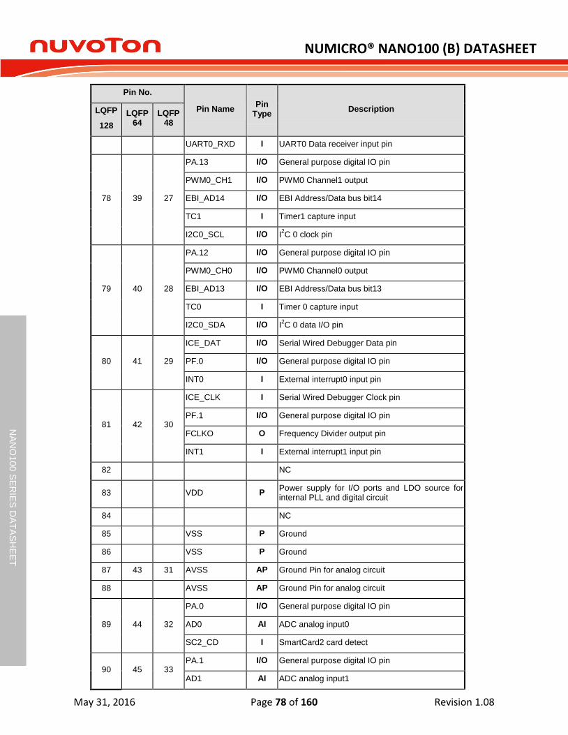
NUMICRO® NANO100 (B) DATASHEET
May 31, 2016 Page 78 of 160 Revision 1.08
NA
NO
10
0 S
ER
IES
DA
TA
SH
EE
T
Pin No.
Pin Name Pin
Type Description LQFP
128
LQFP 64
LQFP 48
UART0_RXD I UART0 Data receiver input pin
78 39 27
PA.13 I/O General purpose digital IO pin
PWM0_CH1 I/O PWM0 Channel1 output
EBI_AD14 I/O EBI Address/Data bus bit14
TC1 I Timer1 capture input
I2C0_SCL I/O I2C 0 clock pin
79 40 28
PA.12 I/O General purpose digital IO pin
PWM0_CH0 I/O PWM0 Channel0 output
EBI_AD13 I/O EBI Address/Data bus bit13
TC0 I Timer 0 capture input
I2C0_SDA I/O I2C 0 data I/O pin
80 41 29
ICE_DAT I/O Serial Wired Debugger Data pin
PF.0 I/O General purpose digital IO pin
INT0 I External interrupt0 input pin
81 42 30
ICE_CLK I Serial Wired Debugger Clock pin
PF.1 I/O General purpose digital IO pin
FCLKO O Frequency Divider output pin
INT1 I External interrupt1 input pin
82 NC
83 VDD P Power supply for I/O ports and LDO source for internal PLL and digital circuit
84 NC
85 VSS P Ground
86 VSS P Ground
87 43 31 AVSS AP Ground Pin for analog circuit
88 AVSS AP Ground Pin for analog circuit
89 44 32
PA.0 I/O General purpose digital IO pin
AD0 AI ADC analog input0
SC2_CD I SmartCard2 card detect
90 45 33 PA.1 I/O General purpose digital IO pin
AD1 AI ADC analog input1

NUMICRO® NANO100 (B) DATASHEET
May 31, 2016 Page 79 of 160 Revision 1.08
NA
NO
10
0 S
ER
IES
DA
TA
SH
EE
T
Pin No.
Pin Name Pin
Type Description LQFP
128
LQFP 64
LQFP 48
EBI_AD12 I/O EBI Address/Data bus bit12
91 46 34
PA.2 I/O General purpose digital IO pin
AD2 AI ADC analog input2
EBI_AD11 I/O EBI Address/Data bus bit11
UART1_RXD I UART1 Data receiver input pin
92 47 35
PA.3 I/O General purpose digital IO pin
AD3 AI ADC analog input3
EBI_AD10 I/O EBI Address/Data bus bit10
UART1_TXD O UART1 Data transmitter output pin
93 48 36
PA.4 I/O Digital GPIO pin
AD4 AI ADC analog input4
EBI_AD9 I/O EBI Address/Data bus bit9
SC2_PWR O SmartCard2 Power pin
I2C0_SDA I/O I2C 0 data I/O pin
94 49 37
PA.5 I/O General purpose digital IO pin
AD5 AI ADC analog input5
EBI_AD8 I/O EBI Address/Data bus bit8
SC2_RST O SmartCard2 RST pin
I2C0_SCL I/O I2C 0 clock pin
95 50 38
PA.6 I/O General purpose digital IO pin
AD6 AI ADC analog input6
EBI_AD7 I/O EBI Address/Data bus bit7
TC3 I Timer3 capture input
SC2_CLK O SmartCard2 clock pin(SC2_UART_TXD)
PWM0_CH3 O PWM0 Channel3 output
96
PA.7 I/O General purpose digital IO pin
AD7 AI ADC analog input7
EBI_AD6 I/O EBI Address/Data bus bit6
TC2 I Timer2 capture input
SC2_DAT I/O SmartCard2 DATA pin(SC2_UART_RXD)

NUMICRO® NANO100 (B) DATASHEET
May 31, 2016 Page 80 of 160 Revision 1.08
NA
NO
10
0 S
ER
IES
DA
TA
SH
EE
T
Pin No.
Pin Name Pin
Type Description LQFP
128
LQFP 64
LQFP 48
PWM0_CH2 O PWM0 Channel2 output
97 51 39 VREF AP Voltage reference input for ADC
98 NC
99 52 40 AVDD AP Power supply for internal analog circuit
100
PD.0 I/O General purpose digital IO pin
UART1_RXD I UART1 Data receiver input pin
SPI2_SS0 I/O SPI2 1st slave select pin
SC1_CLK O SmartCard1 clock pin(SC1_UART_TXD)
AD8 AI ADC analog input8
101
PD.1 I/O General purpose digital IO pin
UART1_TXD O UART1 Data transmitter output pin
SPI2_CLK I/O SPI2 serial clock pin
SC1_DAT I/O SmartCard1 DATA pin(SC1_UART_RXD)
AD9 AI ADC analog input9
102
PD.2 I/O General purpose digital IO pin
UART1_nRTS O UART1 Request to Send output pin
I2S_LRCLK I/O I2S left right channel clock
SPI2_MISO0 I/O SPI2 1st MISO (Master In, Slave Out) pin
SC1_PWR O SmartCard1 Power pin
AD10 AI ADC analog input10
103
PD.3 I/O General purpose digital IO pin
UART1_nCTS I UART1 Clear to Send input pin
I2S_BCLK I/O I2S bit clock pin
SPI2_MOSI0 I/O SPI2 1st MOSI (Master Out, Slave In) pin
SC1_RST O SmartCard1 RST pin
AD11 AI ADC analog input11
104 NC
105
PD.4 I/O General purpose digital IO pin
I2S_DI I I2S data input
SPI2_MISO1 I/O SPI2 2nd
MISO (Master In, Slave Out) pin

NUMICRO® NANO100 (B) DATASHEET
May 31, 2016 Page 81 of 160 Revision 1.08
NA
NO
10
0 S
ER
IES
DA
TA
SH
EE
T
Pin No.
Pin Name Pin
Type Description LQFP
128
LQFP 64
LQFP 48
SC1_CD I SmartCard1 card detect
106
PD.5 I/O General purpose digital IO pin
I2S_DO O I2S data output
SPI2_MOSI1 I/O SPI2 2nd
MOSI (Master Out, Slave In) pin
107 53 41
PC.7 I/O General purpose digital IO pin
DA1+OUT AO DAC 1 output
EBI_AD5 I/O EBI Address/Data bus bit5
TC1 I Timer1 capture input
PWM0_CH1 O PWM1 Channel1 output
108 54 42
PC.6 I/O General purpose digital IO pin
DA0_OUT I DAC0 output
EBI_AD4 I/O EBI Address/Data bus bit4
TC0 I Timer 0 capture input
SC1_CD SmartCard1 card detect pin
PWM0_CH0 O PWM0 Channel0 output
109 55
PC.15 I/O General purpose digital IO pin
EBI_AD3 I/O EBI Address/Data bus bit3
TC0 I Timer0 capture input
PWM1_CH2 O PWM1 Channel1 output
110 56
PC.14 I/O General purpose digital IO pin
EBI_AD2 I/O EBI Address/Data bus bit2
PWM1_CH3 I/O PWM1 Channel3 output
111 57 43
PB.15 I/O General purpose digital IO pin
INT1 I External interrupt1 input pin
SNOOPER I Snooper pin
SC1_CD I SmartCard1 card detect
112 NC
113 58 44 XT1_IN O External 4~24 MHz crystal output pin
PF.3 I/O General purpose digital I/O pin
114 59 45 XT1_OUT I External 4~24 MHz crystal input pin

NUMICRO® NANO100 (B) DATASHEET
May 31, 2016 Page 82 of 160 Revision 1.08
NA
NO
10
0 S
ER
IES
DA
TA
SH
EE
T
Pin No.
Pin Name Pin
Type Description LQFP
128
LQFP 64
LQFP 48
PF.2 I/O General purpose digital I/O pin
115 NC
116 60 46 nRESET I External reset input: Low active, set this pin low reset chip to initial state. With internal pull-up.
117 61 VSS P Ground
118 VSS P Ground
119 NC
120 62 VDD P Power supply for I/O ports and LDO source for internal PLL and digital circuit
121 NC
122 PF.4 I/O General purpose digital IO pin
I2C0_SDA I/O I2C 0 data I/O pin
123 PF.5 I/O General purpose digital IO pin
I2C0_SCL I/O I2C 0 clock pin
124 VSS P Ground
125 63 47 PVSS P PLL Ground
126 64 48
PB.8 I/O General purpose digital IO pin
STADC I ADC external trigger input.
TM0 I Timer0 external counter input
INT0 I External interrupt0 input pin
SC2_PWR O SmartCard2 Power pin
127 PE.15 I/O General purpose digital IO pin
128 PE.14 I/O General purpose digital IO pin
Note:
1. Pin Type: I = Digital Input, O=Digital Output; AI=Analog Input; AO= Analog Output; P=Power Pin; AP=Analog Power;

NUMICRO® NANO100 (B) DATASHEET
May 31, 2016 Page 83 of 160 Revision 1.08
NA
NO
10
0 S
ER
IES
DA
TA
SH
EE
T
3.4.4 NuMicro® Nano130 Pin Description
Pin No.
Pin Name Pin
Type Description
LQFP 128-pin
LQFP 64-pin
LQFP 48-pin
1 PE.13 I/O General purpose digital I/O pin
LCD_SEG27 O LCD segment output 27 at LQFP128
2 1
PB.14 I/O General purpose digital I/O pin
INT0 I External interrupt0 input pin
SC2_CD I SmartCard2 card detect
SPI2_SS1 I/O SPI2 2nd
slave select pin
LCD_SEG12 O LCD segment output 12 at LQFP64
LCD_SEG26 O LCD segment output 26 at LQFP128
3 2
PB.13 I/O General purpose digital I/O pin
EBI_AD1 I/O EBI Address/Data bus bit1
LCD_SEG11 O LCD segment output 11 at LQFP64
LCD_SEG25 O LCD segment output 25 at LQFP128
4 3
PB.12 I/O General purpose digital I/O pin
EBI_AD0 I/O EBI Address/Data bus bit0
FCLKO O Frequency Divider output pin
LCD_SEG10 O LCD segment output 10 at LQFP64
LCD_SEG24 O LCD segment output 24 at LQFP128
5 NC
6 4 X32O O External 32.768 kHz crystal output pin
7 5 X32I I External 32.768 kHz crystal input pin
8 NC
9 6
PA.11 I/O General purpose digital I/O pin
I2C1_SCL I/O I2C1 clock pin
EBI_nRD O EBI read enable output pin
SC0_RST O SmartCard0 RST pin
SPI2_MOSI0 I/O SPI2 1st MOSI (Master Out, Slave In) pin
LCD_SEG9 O LCD segment output 9 at LQFP64
LCD_SEG23 O LCD segment output 23 at LQFP128
10 7 PA.10 I/O General purpose digital I/O pin
I2C1_SDA I/O I2C1 data I/O pin
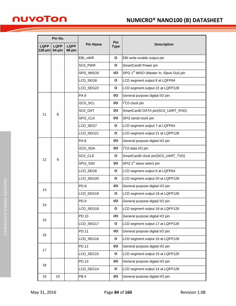
NUMICRO® NANO100 (B) DATASHEET
May 31, 2016 Page 84 of 160 Revision 1.08
NA
NO
10
0 S
ER
IES
DA
TA
SH
EE
T
Pin No.
Pin Name Pin
Type Description
LQFP 128-pin
LQFP 64-pin
LQFP 48-pin
EBI_nWR O EBI write enable output pin
SC0_PWR O SmartCard0 Power pin
SPI2_MISO0 I/O SPI2 1st MISO (Master In, Slave Out) pin
LCD_SEG8 O LCD segment output 8 at LQFP64
LCD_SEG22 O LCD segment output 22 at LQFP128
11 8
PA.9 I/O General purpose digital I/O pin
I2C0_SCL I/O I2C0 clock pin
SC0_DAT I/O SmartCard0 DATA pin(SC0_UART_RXD)
SPI2_CLK I/O SPI2 serial clock pin
LCD_SEG7 O LCD segment output 7 at LQFP64
LCD_SEG21 O LCD segment output 21 at LQFP128
12 9
PA.8 I/O General purpose digital I/O pin
I2C0_SDA I/O I2C0 data I/O pin
SC0_CLK O SmartCard0 clock pin(SC0_UART_TXD)
SPI2_SS0 I/O SPI2 1st slave select pin
LCD_SEG6 O LCD segment output 6 at LQFP64
LCD_SEG20 O LCD segment output 20 at LQFP128
13 PD.8 I/O General purpose digital I/O pin
LCD_SEG19 O LCD segment output 19 at LQFP128
14 PD.9 I/O General purpose digital I/O pin
LCD_SEG18 O LCD segment output 18 at LQFP128
15 PD.10 I/O General purpose digital I/O pin
LCD_SEG17 O LCD segment output 17 at LQFP128
16 PD.11 I/O General purpose digital I/O pin
LCD_SEG16 O LCD segment output 16 at LQFP128
17 PD.12 I/O General purpose digital I/O pin
LCD_SEG15 O LCD segment output 15 at LQFP128
18 PD.13 I/O General purpose digital I/O pin
LCD_SEG14 O LCD segment output 14 at LQFP128
19 10 PB.4 I/O General purpose digital I/O pin
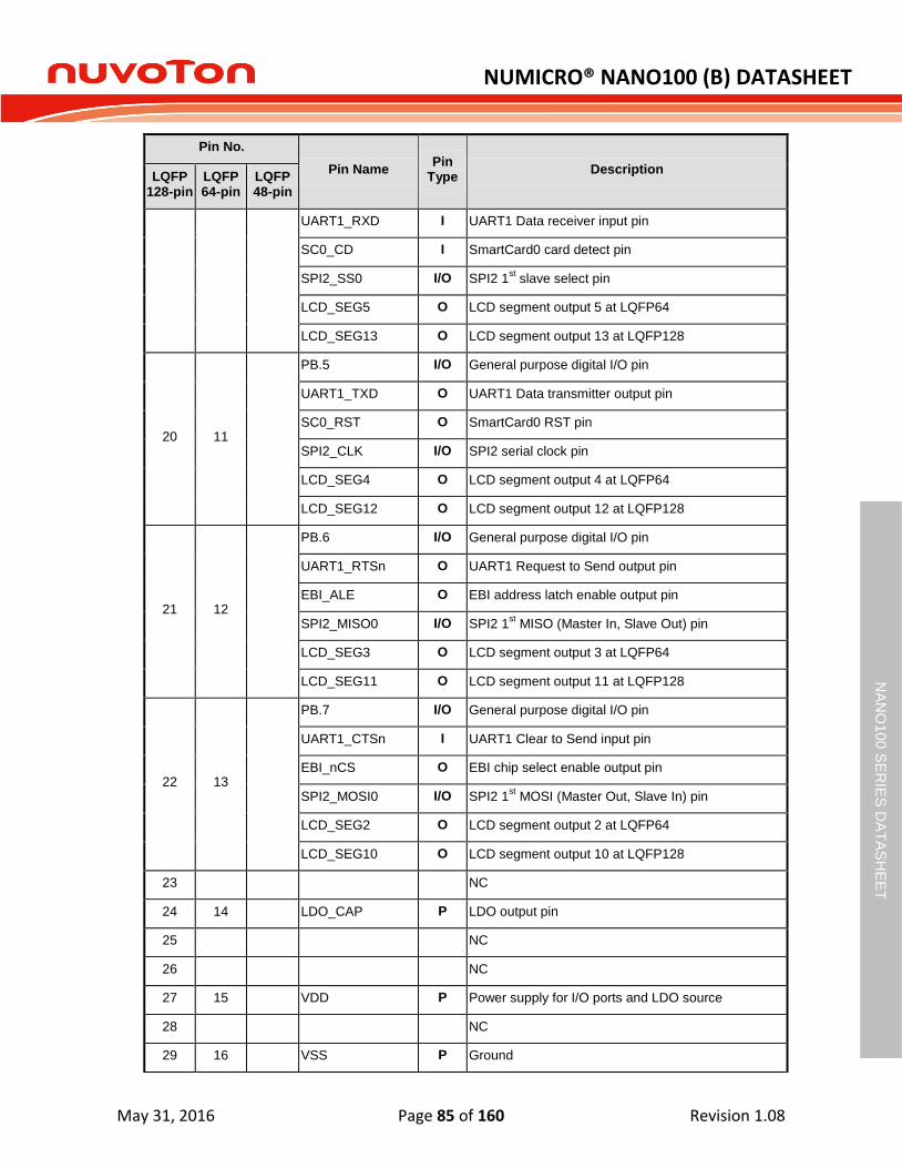
NUMICRO® NANO100 (B) DATASHEET
May 31, 2016 Page 85 of 160 Revision 1.08
NA
NO
10
0 S
ER
IES
DA
TA
SH
EE
T
Pin No.
Pin Name Pin
Type Description
LQFP 128-pin
LQFP 64-pin
LQFP 48-pin
UART1_RXD I UART1 Data receiver input pin
SC0_CD I SmartCard0 card detect pin
SPI2_SS0 I/O SPI2 1st slave select pin
LCD_SEG5 O LCD segment output 5 at LQFP64
LCD_SEG13 O LCD segment output 13 at LQFP128
20 11
PB.5 I/O General purpose digital I/O pin
UART1_TXD O UART1 Data transmitter output pin
SC0_RST O SmartCard0 RST pin
SPI2_CLK I/O SPI2 serial clock pin
LCD_SEG4 O LCD segment output 4 at LQFP64
LCD_SEG12 O LCD segment output 12 at LQFP128
21 12
PB.6 I/O General purpose digital I/O pin
UART1_RTSn O UART1 Request to Send output pin
EBI_ALE O EBI address latch enable output pin
SPI2_MISO0 I/O SPI2 1st MISO (Master In, Slave Out) pin
LCD_SEG3 O LCD segment output 3 at LQFP64
LCD_SEG11 O LCD segment output 11 at LQFP128
22 13
PB.7 I/O General purpose digital I/O pin
UART1_CTSn I UART1 Clear to Send input pin
EBI_nCS O EBI chip select enable output pin
SPI2_MOSI0 I/O SPI2 1st MOSI (Master Out, Slave In) pin
LCD_SEG2 O LCD segment output 2 at LQFP64
LCD_SEG10 O LCD segment output 10 at LQFP128
23 NC
24 14 LDO_CAP P LDO output pin
25 NC
26 NC
27 15 VDD P Power supply for I/O ports and LDO source
28 NC
29 16 VSS P Ground

NUMICRO® NANO100 (B) DATASHEET
May 31, 2016 Page 86 of 160 Revision 1.08
NA
NO
10
0 S
ER
IES
DA
TA
SH
EE
T
Pin No.
Pin Name Pin
Type Description
LQFP 128-pin
LQFP 64-pin
LQFP 48-pin
30 VSS P Ground
31 VSS P Ground
32 VSS P Ground
33 PE.12 I/O General purpose digital I/O pin
34 PE.11 I/O General purpose digital I/O pin
35 PE.10 I/O General purpose digital I/O pin
36 PE.9 I/O General purpose digital I/O pin
37 PE.8 I/O General purpose digital I/O pin
LCD_SEG9 O LCD segment output 9 at LQFP128
38 PE.7 I/O General purpose digital I/O pin
LCD_SEG8 O LCD segment output 8 at LQFP128
39 NC
40 17 USB_VBUS USB POWER SUPPLY: From USB Host or HUB.
41 18 USB_VDD33_CAP USB Internal Power Regulator Output 3.3V Decoupling Pin
42 19 USB_D- USB USB Differential Signal D-
43 20 USB_D+ USB USB Differential Signal D+
44 21
PB.0 I/O General purpose digital I/O pin
UART0_RXD I UART0 Data receiver input pin
SPI1_MOSI0 I/O SPI1 1st MOSI (Master Out, Slave In) pin
LCD_SEG1 O LCD segment output 1 at LQFP64 (or as LCD_COM5)
LCD_SEG7 O LCD segment output 7 at LQFP128
45 22
PB.1 I/O General purpose digital I/O pin
UART0_TXD O UART0 Data transmitter output pin
SPI1_MISO0 I/O SPI1 1st MISO (Master In, Slave Out) pin
LCD_SEG0 O LCD segment output 0 at LQFP64 (or as LCD_COM4)
LCD_SEG6 O LCD segment output 6 at LQFP128
46 23
PB.2 I/O General purpose digital I/O pin
UART0_RTSn O UART0 Request to Send output pin
EBI_nWRL O EBI low byte write enable output pin

NUMICRO® NANO100 (B) DATASHEET
May 31, 2016 Page 87 of 160 Revision 1.08
NA
NO
10
0 S
ER
IES
DA
TA
SH
EE
T
Pin No.
Pin Name Pin
Type Description
LQFP 128-pin
LQFP 64-pin
LQFP 48-pin
SPI1_CLK I/O SPI1 serial clock pin
LCD_COM3 O LCD common output 3 at LQFP64
LCD_SEG5 O LCD segment output 5 at LQFP128
47 24
PB.3 I/O General purpose digital I/O pin
UART0_CTSn I UART0 Clear to Send input pin
EBI_nWRH O EBI high byte write enable output pin
SPI1_SS0 I/O SPI1 1st slave select pin
LCD_COM2 O LCD common output 2 at LQFP64
LCD_SEG4 O LCD segment output 4 at LQFP128
48 PD.6 I/O General purpose digital I/O pin
LCD_SEG3 O LCD segment output 3 at LQFP128
49 PD.7 I/O General purpose digital I/O pin
LCD_SEG2 O LCD segment output 2 at LQFP128
50
PD.14 I/O General purpose digital I/O pin
LCD_SEG1 O LCD segment output 1 at LQFP128 (or as LCD_COM5)
51
PD.15 I/O General purpose digital I/O pin
LCD_SEG0 O LCD segment output 0 at LQFP128 (or as LCD_COM4)
52
PC.5 I/O General purpose digital I/O pin
SPI0_MOSI1 I/O SPI0 2nd
MOSI (Master Out, Slave In) pin
LCD_COM3 O LCD common output 3 at LQFP128
53
PC.4 I/O General purpose digital I/O pin
SPI0_MISO1 I/O SPI0 2nd
MISO (Master In, Slave Out) pin
LCD_COM2 O LCD common output 2 at LQFP128
54 25
PC.3 I/O General purpose digital I/O pin
SPI0_MOSI0 I/O SPI0 1st MOSI (Master Out, Slave In) pin
I2S_DO O I2S data output
SC1_RST O SmartCard1 RST pin
LCD_COM1 O LCD common output 1 at LQFP64
LCD_COM1 O LCD common output 1 at LQFP128

NUMICRO® NANO100 (B) DATASHEET
May 31, 2016 Page 88 of 160 Revision 1.08
NA
NO
10
0 S
ER
IES
DA
TA
SH
EE
T
Pin No.
Pin Name Pin
Type Description
LQFP 128-pin
LQFP 64-pin
LQFP 48-pin
55 26
PC.2 I/O General purpose digital I/O pin
SPI0_MISO0 I/O SPI0 1st MISO (Master In, Slave Out) pin
I2S_DI I I2S data input
SC1_PWR O SmartCard1 PWR pin
LCD_COM0 O LCD common output 0 at LQFP64
LCD_COM0 O LCD common output 0 at LQFP128
56 27
PC.1 I/O General purpose digital I/O pin
SPI0_CLK I/O SPI0 serial clock pin
I2S_BCLK I/O I2S bit clock pin
SC1_DAT I/O SmartCard1 DATA pin(SC1_UART_RXD)
LCD_DH2 O LCD externl capacitor pin of charge pump circuit at LQFP64
LCD_DH2 O LCD externl capacitor pin of charge pump circuit at LQFP128
57 28
PC.0 / MCLKO I/O General purpose digital I/O pin / Module clock output pin
SPI0_SS0 I/O SPI0 1st slave select pin
I2S_LRCLK I/O I2S left right channel clock
SC1_CLK O SmartCard1 clock pin(SC1_UART_TXD)
LCD_DH1 O LCD externl capacitor pin of charge pump circuit at LQFP64
LCD_DH1 O LCD externl capacitor pin of charge pump circuit at LQFP128
58 PE.6 I/O General purpose digital I/O pin
59 29 LCD_VLCD AO LCD power supply pin
60 NC
61 PE.5 General purpose digital I/O pin
62 30
PB.11 I/O General purpose digital I/O pin
PWM1_CH0 I/O PWM1 Channel0 output
TM3 O Timer3 external counter input
SC2_DAT I/O SmartCard2 DATA pin(SC2_UART_RXD)
SPI0_MISO0 I/O SPI0 1st MISO (Master In, Slave Out) pin

NUMICRO® NANO100 (B) DATASHEET
May 31, 2016 Page 89 of 160 Revision 1.08
NA
NO
10
0 S
ER
IES
DA
TA
SH
EE
T
Pin No.
Pin Name Pin
Type Description
LQFP 128-pin
LQFP 64-pin
LQFP 48-pin
LCD_V1 O LCD Unit voltage for LCD charge pump circuit at LQFP64
LCD_V1 O LCD Unit voltage for LCD charge pump circuit at LQFP128
63 31
PB.10 I/O General purpose digital I/O pin
SPI0_SS1 I/O SPI0 2nd
slave select pin
TM2 O Timer2 external counter input
SC2_CLK O SmartCard2 clock pin(SC2_UART_TXD)
SPI0_MOSI0 I/O SPI0 1st MOSI (Master Out, Slave In) pin
LCD_V2 O LCD driver biasing voltage at LQFP64
LCD_V2 O LCD driver biasing voltage at LQFP128
64 32
PB.9 I/O General purpose digital I/O pin
SPI1_SS1 I/O SPI1 2nd
slave select pin
TM1 O Timer1 external counter input
SC2_RST O SmartCard2 RST pin
INT0 I External interrupt0 input pin
LCD_V3 O LCD driver biasing voltage at LQFP64
LCD_V3 O LCD driver biasing voltage at LQFP128
65 PE.4 I/O General purpose digital I/O pin
SPI0_MOSI0 I/O SPI0 1st MOSI (Master Out, Slave In) pin
66 PE.3 I/O General purpose digital I/O pin
SPI0_MISO0 I/O SPI0 1st MISO (Master In, Slave Out) pin
67 PE.2 I/O General purpose digital I/O pin
SPI0_CLK I/O SPI0 serial clock pin
68
PE.1 I/O General purpose digital I/O pin
PWM1_CH3 I/O PWM1 Channel3 output
SPI0_SS0 I/O SPI0 1st slave select pin
69
PE.0 I/O General purpose digital I/O pin
PWM1_CH2 I/O PWM1 Channel2 output
I2S_MCLK O I2S master clock output pin
70 PC.13 I/O General purpose digital I/O pin

NUMICRO® NANO100 (B) DATASHEET
May 31, 2016 Page 90 of 160 Revision 1.08
NA
NO
10
0 S
ER
IES
DA
TA
SH
EE
T
Pin No.
Pin Name Pin
Type Description
LQFP 128-pin
LQFP 64-pin
LQFP 48-pin
SPI1_MOSI1 I/O SPI1 2nd
MOSI (Master Out, Slave In) pin
PWM1_CH1 O PWM1 Channel1 output
SNOOPER I Snooper pin
INT1 I External interrupt 1 input pin
I2C0_SCL O I2C0 clock pin
71
PC.12 I/O General purpose digital I/O pin
SPI1_MISO1 I/O SPI1 2nd
MISO (Master In, Slave Out) pin
PWM1_CH0 O PWM1 Channel0 output
INT0 I External interrupt0 input pin
I2C0_SDA I/O I2C0 data I/O pin
72 33
PC.11 I/O General purpose digital I/O pin
SPI1_MOSI0 I/O SPI1 1st MOSI (Master Out, Slave In) pin
UART1_TXD O UART1 Data transmitter output pin
LCD_SEG31 O LCD segment output 31 at LQFP64
73 34
PC.10 I/O General purpose digital I/O pin
SPI1_MISO0 I/O SPI1 1st MISO (Master In, Slave Out) pin
UART1_RXD I UART1 Data receiver input pin
LCD_SEG30 O LCD segment output 30 at LQFP64
74 35
PC.9 I/O General purpose digital I/O pin
SPI1_CLK I/O SPI1 serial clock pin
I2C1_SCL I/O I2C1 clock pin
LCD_SEG29 O LCD segment output 29 at LQFP64
75 36
PC.8 I/O General purpose digital I/O pin
SPI1_SS0 I/O SPI1 1st slave select pin
EBI_MCLK O EBI external clock output pin
I2C1_SDA I/O I2C1 data I/O pin
LCD_SEG28 O LCD segment output 28 at LQFP64
76 37
PA.15 I/O General purpose digital I/O pin
PWM0_CH3 I/O PWM0 Channel3 output
I2S_MCLK O I2S master clock output pin

NUMICRO® NANO100 (B) DATASHEET
May 31, 2016 Page 91 of 160 Revision 1.08
NA
NO
10
0 S
ER
IES
DA
TA
SH
EE
T
Pin No.
Pin Name Pin
Type Description
LQFP 128-pin
LQFP 64-pin
LQFP 48-pin
TC3 I Timer3 capture input
SC0_PWR O SmartCard0 Power pin
UART0_TXD O UART0 Data transmitter output pin
LCD_SEG27 O LCD segment output 27 at LQFP64
77 38
PA.14 I/O General purpose digital I/O pin
PWM0_CH2 I/O PWM0 Channel2 output
EBI_AD15 I/O EBI Address/Data bus bit15
TC2 I Timer2 capture input
UART0_RXD I UART0 Data receiver input pin
LCD_SEG26 O LCD segment output 26 at LQFP64
78 39
PA.13 I/O General purpose digital I/O pin
PWM0_CH1 I/O PWM0 Channel1 output
EBI_AD14 I/O EBI Address/Data bus bit14
TC1 I Timer1 capture input
I2C0_SCL I/O I2C0 clock pin
LCD_SEG25 O LCD segment output 25 at LQFP64
79 40
PA.12 I/O General purpose digital I/O pin
PWM0_CH0 I/O PWM0 Channel0 output
EBI_AD13 I/O EBI Address/Data bus bit13
TC0 I Timer0 capture input
I2C0_SDA I/O I2C0 data I/O pin
LCD_SEG24 O LCD segment output 24 at LQFP64
80 41
ICE_DAT I/O Serial Wired Debugger Data pin
PF.0 I/O General purpose digital I/O pin
INT0 I External interrupt0 input pin
81 42
ICE_CLK I Serial Wired Debugger Clock pin
PF.1 I/O General purpose digital I/O pin
FCLKO O Frequency Divider output pin
INT1 I External interrupt1 input pin
82 NC

NUMICRO® NANO100 (B) DATASHEET
May 31, 2016 Page 92 of 160 Revision 1.08
NA
NO
10
0 S
ER
IES
DA
TA
SH
EE
T
Pin No.
Pin Name Pin
Type Description
LQFP 128-pin
LQFP 64-pin
LQFP 48-pin
83 VDD P Power supply for I/O ports and LDO source for internal PLL and digital circuit
84 NC
85 VSS P Ground
86 VSS P Ground
87 43 AVSS AP Ground Pin for analog circuit
88 AVSS AP Ground Pin for analog circuit
89 44
PA.0 I/O General purpose digital I/O pin
AD0 AI ADC analog input0
SC2_CD I SmartCard2 card detect
90 45
PA.1 I/O General purpose digital I/O pin
AD1 AI ADC analog input1
EBI_AD12 I/O EBI Address/Data bus bit12
91 46
PA.2 I/O General purpose digital I/O pin
AD2 AI ADC analog input2
EBI_AD11 I/O EBI Address/Data bus bit11
UART1_RXD I UART1 Data receiver input pin
LCD_SEG23* AO LCD segment output 23 at LQFP64
92 47
PA.3 I/O General purpose digital I/O pin
AD3 AI ADC analog input3
EBI_AD10 I/O EBI Address/Data bus bit10
UART1_TXD O UART1 Data transmitter output pin
LCD_SEG22* AO LCD segment output 22 at LQFP64
93 48
PA.4 I/O General purpose digital I/O pin
AD4 AI ADC analog input4
EBI_AD9 I/O EBI Address/Data bus bit9
SC2_PWR O SmartCard2 Power pin
I2C0_SDA I/O I2C0 data I/O pin
LCD_SEG21* AO LCD segment output 21 at LQFP64
LCD_SEG39* AO LCD segment output 39 at LQFP128
94 49 PA.5 I/O General purpose digital I/O pin

NUMICRO® NANO100 (B) DATASHEET
May 31, 2016 Page 93 of 160 Revision 1.08
NA
NO
10
0 S
ER
IES
DA
TA
SH
EE
T
Pin No.
Pin Name Pin
Type Description
LQFP 128-pin
LQFP 64-pin
LQFP 48-pin
AD5 AI ADC analog input5
EBI_AD8 I/O EBI Address/Data bus bit8
SC2_RST O SmartCard2 RST pin
I2C0_SCL I/O I2C0 clock pin
LCD_SEG20* AO LCD segment output 20 at LQFP64
LCD_SEG38* AO LCD segment output 38 at LQFP128
95 50
PA.6 I/O General purpose digital I/O pin
AD6 AI ADC analog input6
EBI_AD7 I/O EBI Address/Data bus bit7
TC3 I Timer3 capture input
SC2_CLK O SmartCard2 clock pin(SC2_UART_TXD)
PWM0_CH3 O PWM0 Channel3 output
LCD_SEG19* AO LCD segment output 19 at LQFP64
LCD_SEG37* AO LCD segment output 37 at LQFP128
96
PA.7 I/O General purpose digital I/O pin
AD7 AI ADC analog input7
EBI_AD6 I/O EBI Address/Data bus bit6
TC2 I Timer2 capture input
SC2_DAT I/O SmartCard2 DATA pin(SC2_UART_RXD)
PWM0_CH2 O PWM0 Channel2 output
LCD_SEG36* AO LCD segment output 36 output at LQFP128
97 51 VREF AP Voltage reference input for ADC
98 NC
99 52 AVDD AP Power supply for internal analog circuit
100
PD.0 I/O General purpose digital I/O pin
UART1_RXD I UART1 Data receiver input pin
SPI2_SS0 I/O SPI2 1st slave select pin
SC1_CLK O SmartCard1 clock pin(SC1_UART_TXD)
AD8 AI ADC analog input8
101 PD.1 I/O General purpose digital I/O pin

NUMICRO® NANO100 (B) DATASHEET
May 31, 2016 Page 94 of 160 Revision 1.08
NA
NO
10
0 S
ER
IES
DA
TA
SH
EE
T
Pin No.
Pin Name Pin
Type Description
LQFP 128-pin
LQFP 64-pin
LQFP 48-pin
TX1 O UART1 Data transmitter output pin
SPI2_CLK I/O SPI2 serial clock pin
SC1_DAT I/O SmartCard1 DATA pin(SC1_UART_RXD)
AD9 AI ADC analog input9
102
PD.2 I/O General purpose digital I/O pin
UART1_RTSn O UART1 Request to Send output pin
I2S_LRCLK I/O I2S left right channel clock
SPI2_MISO0 I/O SPI2 1st MISO (Master In, Slave Out) pin
SC1_PWR O SmartCard1 Power pin
AD10 AI ADC analog input10
103
PD.3 I/O General purpose digital I/O pin
UART1_CTSn I UART1 Clear to Send input pin
I2S_BCLK I/O I2S bit clock pin
SPI2_MOSI0 I/O SPI2 1st MOSI (Master Out, Slave In) pin
SC1_RST O SmartCard1 RST pin
AD11 AI ADC analog input11
104 NC
105
PD.4 I/O General purpose digital I/O pin
I2S_DI I I2S data input
SPI2_MISO1 I/O SPI2 2nd
MISO (Master In, Slave Out) pin
SC1_CD I SmartCard1 card detect
LCD_SEG35 AO LCD segment output 35 at LQFP128
106
PD.5 I/O General purpose digital I/O pin
I2S_DO O I2S data output
SPI2_MOSI1 I/O SPI2 2nd
MOSI (Master Out, Slave In) pin
LCD_SEG34 AO LCD segment output 34 at LQFP128
107 53
PC.7 I/O General purpose digital I/O pin
DA1_OUT AO DAC 1 output
EBI_AD5 I/O EBI Address/Data bus bit5
TC1 I Timer1 capture input

NUMICRO® NANO100 (B) DATASHEET
May 31, 2016 Page 95 of 160 Revision 1.08
NA
NO
10
0 S
ER
IES
DA
TA
SH
EE
T
Pin No.
Pin Name Pin
Type Description
LQFP 128-pin
LQFP 64-pin
LQFP 48-pin
PWM0_CH1 O PWM1 Channel1 output
LCD_SEG17* AO LCD segment output 17 at LQFP64
108 54
PC.6 I/O General purpose digital I/O pin
DA0_OUT I DAC0 output
EBI_AD4 I/O EBI Address/Data bus bit4
TC0 I Timer0 capture input
SC1_CD SmartCard1 card detect pin
PWM0_CH0 O PWM0 Channel0 output
109 55
PC.15 I/O General purpose digital I/O pin
EBI_AD3 I/O EBI Address/Data bus bit3
TC0 I Timer0 capture input
PWM1_CH2 O PWM1 Channel1 output
LCD_SEG16 AO LCD segment output 16 at LQFP64
LCD_SEG33 AO LCD segment output 33 at LQFP128
110 56
PC.14 I/O General purpose digital I/O pin
EBI_AD2 I/O EBI Address/Data bus bit2
PWM1_CH3 I/O PWM1 Channel3 output
LCD_SEG15 AO LCD segment output 15 at LQFP64
LCD_SEG32 AO LCD segment output 32 at LQFP128
111 57
PB.15 I/O General purpose digital I/O pin
INT1 I External interrupt1 input pin
SNOOPER I Snooper pin
SC1_CD I SmartCard1 card detect
LCD_SEG14 AO LCD segment output 14 at LQFP64
LCD_SEG31 AO LCD segment output 31 at LQFP128
112 NC
113 58 XT1_IN O External 4~24 MHz crystal output pin
PF.3 I/O General purpose digital I/O pin
114 59 XT1_OUT I External 4~24 MHz crystal input pin
PF.2 I/O General purpose digital I/O pin
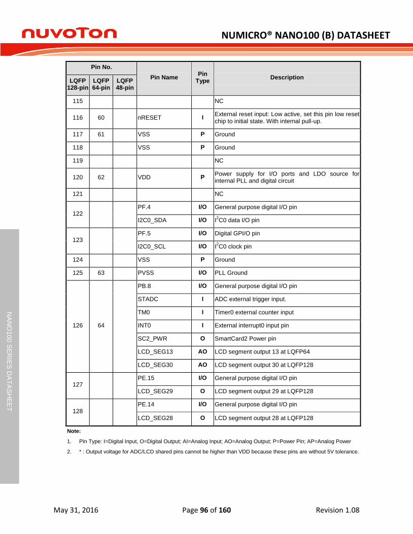
NUMICRO® NANO100 (B) DATASHEET
May 31, 2016 Page 96 of 160 Revision 1.08
NA
NO
10
0 S
ER
IES
DA
TA
SH
EE
T
Pin No.
Pin Name Pin
Type Description
LQFP 128-pin
LQFP 64-pin
LQFP 48-pin
115 NC
116 60 nRESET I External reset input: Low active, set this pin low reset chip to initial state. With internal pull-up.
117 61 VSS P Ground
118 VSS P Ground
119 NC
120 62 VDD P Power supply for I/O ports and LDO source for internal PLL and digital circuit
121 NC
122 PF.4 I/O General purpose digital I/O pin
I2C0_SDA I/O I2C0 data I/O pin
123 PF.5 I/O Digital GPI/O pin
I2C0_SCL I/O I2C0 clock pin
124 VSS P Ground
125 63 PVSS I/O PLL Ground
126 64
PB.8 I/O General purpose digital I/O pin
STADC I ADC external trigger input.
TM0 I Timer0 external counter input
INT0 I External interrupt0 input pin
SC2_PWR O SmartCard2 Power pin
LCD_SEG13 AO LCD segment output 13 at LQFP64
LCD_SEG30 AO LCD segment output 30 at LQFP128
127 PE.15 I/O General purpose digital I/O pin
LCD_SEG29 O LCD segment output 29 at LQFP128
128 PE.14 I/O General purpose digital I/O pin
LCD_SEG28 O LCD segment output 28 at LQFP128
Note:
1. Pin Type: I=Digital Input, O=Digital Output; AI=Analog Input; AO=Analog Output; P=Power Pin; AP=Analog Power
2. * : Output voltage for ADC/LCD shared pins cannot be higher than VDD because these pins are without 5V tolerance.
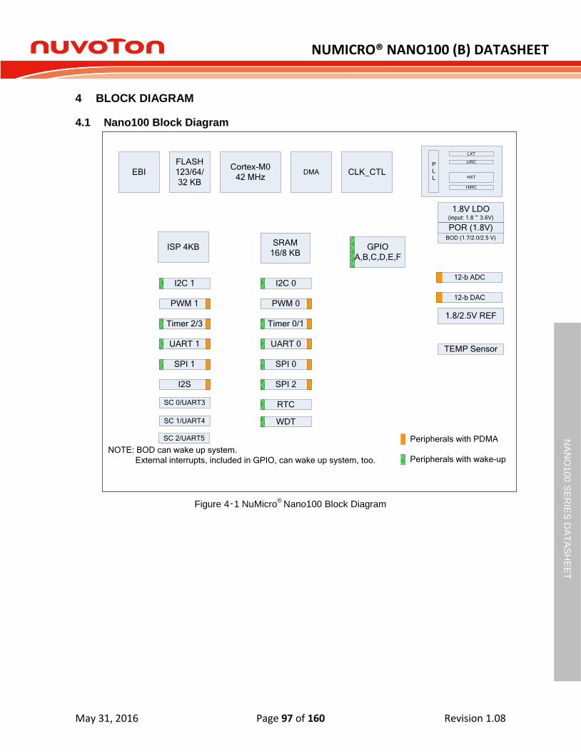
NUMICRO® NANO100 (B) DATASHEET
May 31, 2016 Page 97 of 160 Revision 1.08
NA
NO
10
0 S
ER
IES
DA
TA
SH
EE
T
4 BLOCK DIAGRAM
4.1 Nano100 Block Diagram
Peripherals with PDMA
EBI
FLASH
123/64/
32 KB
Cortex-M0
42 MHzDMA CLK_CTL
ISP 4KBSRAM
16/8 KB
PWM 1
Timer 2/3
UART 1
SPI 1
I2S
I2C 1 I2C 0
PWM 0
Timer 0/1
UART 0
SPI 0
SPI 2
RTC
1.8/2.5V REF
1.8V LDO (input: 1.8 ~ 3.6V)
POR (1.8V)BOD (1.7/2.0/2.5 V)
SC 0/UART3
TEMP Sensor
WDT
Peripherals with wake-up NOTE: BOD can wake up system.
External interrupts, included in GPIO, can wake up system, too.
SC 1/UART4
GPIO
A,B,C,D,E,F
P
L
L HXT
LXT
HIRC
LIRC
12-b ADC
12-b DAC
SC 2/UART5
Figure 4‑1 NuMicro®
Nano100 Block Diagram

NUMICRO® NANO100 (B) DATASHEET
May 31, 2016 Page 98 of 160 Revision 1.08
NA
NO
10
0 S
ER
IES
DA
TA
SH
EE
T
4.2 Nano110 Block Diagram
Peripherals with PDMA
EBI
FLASH
123/64/
32 KB
Cortex-M0
42 MHzDMA CLK_CTL
ISP 4KB SRAM
16/8 KB
PWM 1
Timer 2/3
UART 1
SPI 1
I2S
I2C 1 I2C 0
PWM 0
Timer 0/1
UART 0
SPI 0
SPI 2
RTC
LCD
1.8/2.5V REF
LCD COM/SEG
Up to
4x40/6x38
1.8V LDO (input: 1.8 ~ 3.6V)
POR (1.8V)BOD (1.7/2.0/2.5 V)
SC 0/UART3
TEMP Sensor
WDT
Peripherals with wake-up NOTE: BOD can wake up system.
External interrupts, included in GPIO, can wake up system, too.
SC 1/UART4
GPIO
A,B,C,D,E,F
LCD Booster
P
L
L HXT
LXT
HIRC
LIRC
12-b ADC
12-b DAC
SC 2/UART5
Figure 4‑2 NuMicro®
Nano110 Block Diagram

NUMICRO® NANO100 (B) DATASHEET
May 31, 2016 Page 99 of 160 Revision 1.08
NA
NO
10
0 S
ER
IES
DA
TA
SH
EE
T
4.3 Nano120 Block Diagram
Peripherals with PDMA
EBI
FLASH
123/64/
32 KB
Cortex-M0
42 MHzDMA CLK_CTL
ISP 4KB SRAM
16/8 KB
PWM 1
Timer 2/3
UART 1
SPI 1
I2S
I2C 1 I2C 0
PWM 0
Timer 0/1
UART 0
SPI 0
SPI 2
RTC USB -512B USB PHY
1.8/2.5V REF
1.8V LDO (input: 1.8 ~ 3.6V)
POR (1.8V)BOD (1.7/2.0/2.5 V)
SC 0/UART3
TEMP Sensor
WDT
Peripherals with wake-up NOTE: BOD can wake up system.
External interrupts, included in GPIO, can wake up system, too.
SC 1/UART4
GPIO
A,B,C,D,E,F
P
L
L HXT
LXT
HIRC
LIRC
12-b ADC
12-b DAC
SC 2/UART5
Figure 4‑3 NuMicro®
Nano120 Block Diagram
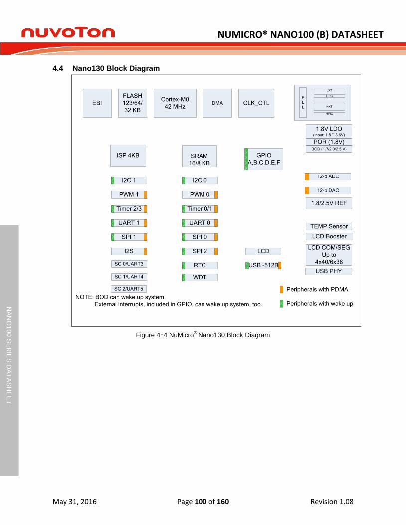
NUMICRO® NANO100 (B) DATASHEET
May 31, 2016 Page 100 of 160 Revision 1.08
NA
NO
10
0 S
ER
IES
DA
TA
SH
EE
T
4.4 Nano130 Block Diagram
Peripherals with PDMA
EBI
FLASH
123/64/
32 KB
Cortex-M0
42 MHzDMA CLK_CTL
ISP 4KB SRAM
16/8 KB
PWM 1
Timer 2/3
UART 1
SPI 1
I2S
I2C 1 I2C 0
PWM 0
Timer 0/1
UART 0
SPI 0
SPI 2
RTC
LCD
USB -512BUSB PHY
1.8/2.5V REF
LCD COM/SEG
Up to
4x40/6x38
1.8V LDO (input: 1.8 ~ 3.6V)
POR (1.8V)BOD (1.7/2.0/2.5 V)
SC 0/UART3
TEMP Sensor
WDT
Peripherals with wake up NOTE: BOD can wake up system.
External interrupts, included in GPIO, can wake up system, too.
SC 1/UART4
GPIO
A,B,C,D,E,F
LCD Booster
P
L
L HXT
LXT
HIRC
LIRC
12-b ADC
12-b DAC
SC 2/UART5
Figure 4‑4 NuMicro®
Nano130 Block Diagram

NUMICRO® NANO100 (B) DATASHEET
May 31, 2016 Page 101 of 160 Revision 1.08
NA
NO
10
0 S
ER
IES
DA
TA
SH
EE
T
5 FUNCTIONAL DESCRIPTION
5.1 Memory Organization
5.1.1 Overview
The Nano100 provides 4G-byte addressing space. The memory locations assigned to each on-chip modules are shown in following. The detailed register definition, memory space, and programming detailed will be described in the following sections for each on-chip module. The Nano100 series only supports little-endian data format.
5.1.2 Memory Map
The memory locations assigned to each on-chip controllers are shown in the following table.
Address Space Token Modules
Flash & SRAM Memory Space
0x0000_0000 – 0x0001_FFFF FLASH_BA FLASH Memory Space (128KB)
0x2000_0000 – 0x2000_3FFF SRAM_BA SRAM Memory Space (16KB)
0x6000_0000 --- 0x6001_FFFF EXTMEM_BA External Memory Space(128KB)
AHB Modules Space (0x5000_0000 – 0x501F_FFFF)
0x5000_0000 – 0x5000_01FF GCR_BA System Management Control Registers
0x5000_0200 – 0x5000_02FF CLK_BA Clock Control Registers
0x5000_0300 – 0x5000_03FF INT_BA Interrupt Multiplexer Control Registers
0x5000_4000 – 0x5000_7FFF GPIO_BA GPIO Control Registers
0x5000_8000 – 0x5000_BFFF DMA_BA DMA Control Registers
0x5000_C000 – 0x5000_FFFF FMC_BA Flash Memory Control Registers
0x5001_0000 – 0x5001_03FF EBI_BA External Bus Interface Control Registers
APB1 Modules Space (0x4000_0000 ~ 0x400F_FFFF)
0x4000_4000 – 0x4000_7FFF WDT_BA Watchdog Timer Control Registers
0x4000_8000 – 0x4000_BFFF RTC_BA Real Time Clock (RTC) Control Register
0x4001_0000 – 0x4001_3FFF TMR01_BA Timer0 and Timer1 Control Registers
0x4002_0000 – 0x4002_3FFF I2C0_BA I2C0 Interface Control Registers
0x4003_0000 – 0x4003_3FFF SPI0_BA SPI0 with Master/Slave function Control Registers
0x4004_0000 – 0x4004_3FFF PWM0_BA PWM0 Control Registers
0x4005_0000 – 0x4005_3FFF UART0_BA UART0 Control Registers
0x4006_0000 – 0x4006_3FFF USBD_BA USB FS device Controller Registers
0x400A_0000 – 0x400A_3FFF DAC_BA Digital-Analog-Converter (DAC) Control Registers
0x400B_0000 – 0x400B_3FFF LCD_BA LCD Control Registers
0x400D_0000 – 0x400D_3FFF SPI2_BA SPI2 with Master/Slave function Control Registers

NUMICRO® NANO100 (B) DATASHEET
May 31, 2016 Page 102 of 160 Revision 1.08
NA
NO
10
0 S
ER
IES
DA
TA
SH
EE
T
0x400E_0000 – 0x400E_3FFF ADC12_BA 12-bit Analog-Digital-Converter (ADC12) Control Registers
APB2 Modules Space (0x4010_0000 ~ 0x401F_FFFF)
0x4011_0000 – 0x4011_3FFF TMR23_BA Timer2 and Timer3 Control Registers
0x4012_0000 – 0x4012_3FFF I2C1_BA I2C1 Interface Control Registers
0x4013_0000 – 0x4013_3FFF SPI1_BA SPI1 with Master/Slave function Control Registers
0x4014_0000 – 0x4014_3FFF PWM1_BA PWM1 Control Registers
0x4015_0000 – 0x4015_3FFF UART1_BA UART1 Control Registers
0x4019_0000 – 0x4019_3FFF SC0_BA SmartCard0 Control Registers
0x401A_0000 – 0x401A_3FFF I2S_BA I2S Control Registers
0x401B_0000 – 0x401B_3FFF SC1_BA SmartCard1 Control Registers
0x401C_0000 – 0x401C_3FFF SC2_BA SmartCard2 Control Registers
System Control Space (0xE000_E000 ~ 0xE000_EFFF)
0xE000_E010 – 0xE000_E0FF SCS_BA System Timer Control Registers
0xE000_E100 – 0xE000_ECFF SCS_BA External Interrupt Controller Control Registers
0xE000_ED00 – 0xE000_ED8F SCS_BA System Control Registers

NUMICRO® NANO100 (B) DATASHEET
May 31, 2016 Page 103 of 160 Revision 1.08
NA
NO
10
0 S
ER
IES
DA
TA
SH
EE
T
5.2 Nested Vectored Interrupt Controller (NVIC)
5.2.1 Overview
The Cortex-M0 provides an interrupt controller as an integral part of the exception mode, named as “Nested Vectored Interrupt Controller (NVIC)”. It is closely coupled to the processor kernel and provides following features:
5.2.2 Features
Nested and Vectored interrupt support
Automatic processor state saving and restoration
Dynamic priority changing
Reduced and deterministic interrupt latency
The NVIC prioritizes and handles all supported exceptions. All exceptions are handled in “Handler Mode”. This NVIC architecture supports 32 (IRQ[31:0]) discrete interrupts with 4 levels of priority. All of the interrupts and most of the system exceptions can be configured to different priority levels. When an interrupt occurs, the NVIC will compare the priority of the new interrupt to the current running one’s priority. If the priority of the new interrupt is higher than the current one, the new interrupt handler will override the current handler.
When any interrupts is accepted, the starting address of the interrupt service routine (ISR) is fetched from a vector table in memory. There is no need to determine which interrupt is accepted and branch to the starting address of the correlated ISR by software. While the starting address is fetched, NVIC will also automatically save processor state including the registers “PC, PSR, LR, R0~R3, R12” to the stack. At the end of the ISR, the NVIC will restore the mentioned registers from stack and resume the normal execution. Thus it will take less and deterministic time to process the interrupt request.
The NVIC supports “Tail Chaining” which handles back-to-back interrupts efficiently without the overhead of states saving and restoration and therefore reduces delay time in switching to pending ISR at the end of current ISR. The NVIC also supports “Late Arrival” which improves the efficiency of concurrent ISRs. When a higher priority interrupt request occurs before the current ISR starts to execute (at the stage of state saving and starting address fetching), the NVIC will give priority to the higher one without delay penalty. Thus it advances the real-time capability.
For more detailed information, please refer to the “ARM® Cortex™-M0 Technical Reference
Manual” and “ARM® v6-M Architecture Reference Manual”.
NUMICRO® NANO100 (B) DATASHEET
May 31, 2016 Page 104 of 160 Revision 1.08
NA
NO
10
0 S
ER
IES
DA
TA
SH
EE
T
5.3 System Manager
5.3.1 Overview
System manager mainly controls the power modes, wake-up source, system resets and system memory map. It also provides information about product ID, chip reset, IP reset, and multi-function pin control.
5.3.2 Features
Power modes and wake-up sources
System resets
System Memory Map
System manager registers for :
Product ID
Chip and IP reset
Multi-functional pin control

NUMICRO® NANO100 (B) DATASHEET
May 31, 2016 Page 105 of 160 Revision 1.08
NA
NO
10
0 S
ER
IES
DA
TA
SH
EE
T
5.4 Clock Controller
5.4.1 Overview
The clock controller generates clocks for the whole chip, Iincluding system clocks (CPU clock, HCLKx, and PCLKx) and all peripheral engine clocks. HCLKx means AHB bus clock for peripherals on AHB bus. PCLKx means APB bus clock for peripherals on APB bus. The clock controller also implements the power control function with the individually clock ON/OFF control, clock source selection and a 4-bit clock divider. The chip will not enter power-down mode until CPU sets the power down enable bit (PD_EN) and CPU executes the WFI instruction. In the Power-down mode, clock controller turns off the external high frequency crystal, internal high frequency oscillator, and system clocks (CPU clock, HCLKx, and PCLKx) to reduce the power consumption to minimum.
5.4.2 Features
Generates clocks for system clocks and all peripheral engine clocks.
Each peripheral engine clock can be turned on/off.
High frequency crystal, internal high frequency oscillator, and system clocks will be turned off when chip is in Power-down mode.
NUMICRO® NANO100 (B) DATASHEET
May 31, 2016 Page 106 of 160 Revision 1.08
NA
NO
10
0 S
ER
IES
DA
TA
SH
EE
T
5.5 Analog to Digital Converter (ADC)
5.5.1 Overview
This chip contains one 12-bit successive approximation analog-to-digital converter (SAR A/D converter) with 12 external input channels and 6 internal channels. The A/D converter supports three operation modes: Single, Single-cycle Scan and Continuous Scan mode, and can be started by software and external STADC/PB.8 pin and timer event start.
Note that the I/O pins used as ADC analog input pins must be configured as input type and off digital function (GPIOA_OFFD) should be turned on before ADC function is enabled.
5.5.2 Features
Analog input voltage range: 0~Vref (Max to 3.6V)
Selectable 12-bits, 10-bits, 8-bits and 6-bits resolution
Supports sampling time settings (in ADC_CLK unit) for channel 0~11 individually and channel 12~17 share the same one sampling time setting
Supports two power-down modes:
Power-down mode
Standby mode
Up to 12 external analog input channels (channel0 ~ channel11), and 6 internal channels (channel12~channel17) converting six voltage sources, including DAC0, DAC1, internal band-gap voltage, internal temperature sensor output, AVDD, and AVSS.
Maximum ADC clock frequency is 42 MHz and each conversion is 19 clocks+ sampling time depending on the input resistance.
Three operating modes
Single mode: A/D conversion is performed one time on a specified channel.
Single-cycle Scan mode: A/D conversion is performed one cycle on all specified channels with the sequence from the lowest numbered channel to the highest numbered channel.
Continuous Scan mode: A/D converter continuously performs Single-cycle scan mode until software stops A/D conversion.
An A/D conversion can be started by:
Software write 1 to ADST bit
External pin STADC
Selects one from four timer events (TMR0, TMR1, TMR2 and TMR3) that enable ADC and transfer AD results by PDMA
Conversion results held in data registers for each channel
Conversion result can be compared with a specified value and user can select whether to generate an interrupt when conversion result is equal to the compare register setting.
Supports Calibration and load Calibration words capability.

NUMICRO® NANO100 (B) DATASHEET
May 31, 2016 Page 107 of 160 Revision 1.08
NA
NO
10
0 S
ER
IES
DA
TA
SH
EE
T
5.6 Digital to Analog Converter (DAC)
5.6.1 Overview
DAC is a 12-bit voltage-output digital-to-analog converter. Two DACs are implemented in this chip.
5.6.2 Features
DAC is a 12-bit voltage-output DAC. DAC can use in conjunction with the PDMA controller. When two DACs are present, they may be grouped together for synchronous update operation.
Features:
Int_VREF or VREF or AVDD reference voltage selection
Synchronized update capability for two DACs
DAC maximum conversion rate is 500 KSPS

NUMICRO® NANO100 (B) DATASHEET
May 31, 2016 Page 108 of 160 Revision 1.08
NA
NO
10
0 S
ER
IES
DA
TA
SH
EE
T
5.7 DMA Controller
5.7.1 Overview
The DMA controller contains six channel peripheral direct memory access (PDMA) controllers, a video direct memory access (VDMA) controller and a cyclic redundancy check (CRC) generator. The PDMA controller can transfer data to and from memory or transfer data to and from APB devices. The DMA has eight channels of DMA including one channel VDMA (Memory-to-Memory) and six channels PDMA (Peripheral-to-Memory or Memory-to-Peripheral or Memory-to-Memory) and a CRC controller. For channel0 VDMA, it supports block transfer from memory to memory. For PDMA channel (DMA CH1~CH6), there is one-word buffer as transfer buffer between the Peripherals APB devices and Memory. And for channel 0 VDMA, there is a two-word buffer.
Software can stop the DMA operation by disable PDMA [PDMACEN]/VDMA [VDMACEN]. Software can recognize the completion of a DMA operation by software polling or when it receives an internal DMA interrupt. The DMA controller can increase source or destination address, fixed or wrap around them as well.
The DMA controller also contains a cyclic redundancy check (CRC) generator that can perform CRC calculation with programmable polynomial settings. The CRC engine support CPU PIO mode and DMA transfer mode.
5.7.2 Features
Seven DMA channels and a CRC generator: 1 VDMA channel and 6 PDMA channels. Each channel can support a unidirectional transfer.
AMBA AHB master/slave interface compatible, for data transfer and register read/write.
Hardware round robin priority scheme.
VDMA
Memory-to-memory transfer
Supports block transfer with stride
Supports word/half-word/byte boundary address
Supports address direction: increment and decrement
PDMA
Peripheral-to-memory, memory-to-peripheral, and memory-to-memory transfer
Supports word boundary address
Supports word alignment transfer length in memory-to-memory mode
Supports word/half-word/byte alignment transfer length in peripheral-to-memory and memory-to-peripheral mode
Supports word/half-word/byte transfer data width from/to peripheral
Supports address direction: increment, fixed, and wrap around
Cyclic Redundancy Check (CRC)
Supports four common polynomials CRC-CCITT, CRC-8, CRC-16, and CRC-32
CRC-CCITT: X16
+ X12
+ X5 + 1
CRC-8: X8 + X
2 + X + 1
CRC-16: X16
+ X15
+ X2 + 1
CRC-32: X32
+ X26
+ X23
+ X22
+ X16
+ X12
+ X11
+ X10
+ X8 + X
7 + X
5 + X
4 +
X2 + X + 1

NUMICRO® NANO100 (B) DATASHEET
May 31, 2016 Page 109 of 160 Revision 1.08
NA
NO
10
0 S
ER
IES
DA
TA
SH
EE
T
Programmable seed value
Supports programmable order reverse setting for input data and CRC checksum
Supports programmable 1’s complement setting for input data and CRC checksum
Supports CPU PIO mode or DMA transfer mode
Supports 8/16/32-bit of data width in CPU PIO mode
8-bit write mode: 1-AHB clock cycle operation
16-bit write mode: 2-AHB clock cycle operation
32-bit write mode: 4-AHB clock cycle operation
Supports byte alignment transfer length in CRC DMA mode

NUMICRO® NANO100 (B) DATASHEET
May 31, 2016 Page 110 of 160 Revision 1.08
NA
NO
10
0 S
ER
IES
DA
TA
SH
EE
T
5.8 External Bus Interface
5.8.1 Overview
This chip is equipped with an external bus interface (EBI) to access external device. To save the connections between external device and this chip, EBI support address bus and data bus multiplex mode. Also, address latch enable (ALE) signal is used to differentiate the address and data cycle.
5.8.2 Features
External devices with max. 64 Kbytes size (8-bit data width)/128 Kbytes (16-bit data width) supported
Supports variable external bus base clock (MCLK)
Supports 8-bit or 16-bit data width
Supports variable data access time (tACC), address latch enable time (tALE) and address hold time (tAHD)
Address bus and data bus multiplex mode supported to save the address pins
Configurable idle cycle supported for different access condition: Write command finish (W2X), Read-to-Read (R2R), Read-to-Write (R2W)
Supports PDMA and VDMA transfer

NUMICRO® NANO100 (B) DATASHEET
May 31, 2016 Page 111 of 160 Revision 1.08
NA
NO
10
0 S
ER
IES
DA
TA
SH
EE
T
5.9 FLASH Memory Controller (FMC)
5.9.1 Overview
This chip is equipped with 32K/64K/123K bytes on-chip embedded Flash EPROM for application program memory (APROM) that can be updated through ISP/IAP procedure. In System Programming (ISP) function enables user to update program memory when chip is soldered on PCB. After chip powered on Cortex-M0 CPU fetches code from APROM or LDROM decided by boot select (CBS) in Config0. By the way, this chip also provides DATA Flash Region, the data flash is shared with original program memory and its start address is configurable and defined by user in Config1. The data flash size is defined by user application request.
5.9.2 Features
AHB interface compatible
Run up to 42 MHz with zero wait state for discontinuous address read access
32/64/123KB application program memory (APROM)
4KB in system programming (ISP) loader program memory (LDROM)
Programmable data flash start address and memory size with 512 bytes page erase unit
In System Program (ISP)/In Application Program (IAP) to update on chip Flash EPROM
NUMICRO® NANO100 (B) DATASHEET
May 31, 2016 Page 112 of 160 Revision 1.08
NA
NO
10
0 S
ER
IES
DA
TA
SH
EE
T
5.10 General Purpose I/O Controller
5.10.1 Overview
Up to 86 General Purpose I/O pins can be shared with other function pins; it depends on the chip configuration. These 86 pins are arranged in 6 ports named with GPIOA, GPIOB, GPIOC, GPIOD, GPIOE and GPIOF. Ports A ~ E have the maximum of 16 pins while port F have 6 pins. Each one of the 86 pins is independent and has the corresponding register bits to control the pin mode function and data.
The I/O type of each of I/O pins can be independently software configured as input, output, and open-drain mode. Each I/O pin has a very weak individual pull-up resistor which is about 110
K~300 K for VDD from 1.8 V to 3.6 V.
5.10.2 Features
Up to 86 general purpose I/O pins
Supports Input, Output, Open-drain Operation mode
Programmable de-bounce timing
Each I/O pin can be programmed as either edge-trigger or level-sensitive
Each I/O pin can be programmed as either low-level active or high-level active
Each I/O pin can be programmed as either falling-edge trigger or rising-edge trigger

NUMICRO® NANO100 (B) DATASHEET
May 31, 2016 Page 113 of 160 Revision 1.08
NA
NO
10
0 S
ER
IES
DA
TA
SH
EE
T
5.11 I2C
5.11.1 Overview
I2C is a two-wire, bi-directional serial bus that provides a simple and efficient method of data
exchange between devices. The I2C standard is a true multi-master bus including collision
detection and arbitration that prevents data corruption if two or more masters attempt to control the bus simultaneously. Serial, 8-bit oriented bi-directional data transfers can be made up to 1.0 Mbps.
Data is transferred between a Master and a Slave synchronously to SCL on the SDA line on a byte-by-byte basis. Each data byte is 8-bit long. There is one SCL clock pulse for each data bit with the MSB being transmitted first. An acknowledge bit follows each transferred byte.
A transition on the SDA line while SCL is high is interpreted as a command (START or STOP). Each bit is sampled during the high period of SCL; therefore, the SDA line may be changed only during the low period of SCL and must be held stable during the high period of SCL.
The controller’s on-chip I2C logic provides the serial interface that meets the I
2C bus standard
mode specification. The I2C controller handles byte transfers autonomously. Pull up resistor is
needed for I2C operation as these are open drain pins.
The I2C controller is equipped with two slave address registers. The contents of the registers are
irrelevant when I2C is in Master mode. In the Slave mode, the seven most significant bits must be
loaded with the user’s own slave address. The I2C hardware will react if the contents of I2CADDR
are matched with the received slave address.
This controller supports the “General Call (GC)” function. If the GC bit is set this controller will respond to General Call address (00H). Clear GC bit to disable general call function. When GC bit is set and the I
2C is in Slave mode, it can receive the general call address which is equal to 00H
after master sends general call address to the I2C bus, then it will follow status of GC mode. If it is
in Master mode, the ACK bit must be cleared when it sends general call address of 00H to the I2C
bus.
The I2C-bus controller supports multiple address recognition with two address mask register.
When the bit in the address mask register is set to one, it means the received corresponding address bit is don’t-care. If the bit is set to zero, that means the received corresponding register bit should be exact the same as address register.
NUMICRO® NANO100 (B) DATASHEET
May 31, 2016 Page 114 of 160 Revision 1.08
NA
NO
10
0 S
ER
IES
DA
TA
SH
EE
T
5.11.2 Features
Acts as Master or Slave mode
Bidirectional data transfer between masters and slaves
Multi-master bus (no central master)
Arbitration between simultaneously transmitting masters without corruption of serial data on the bus
Serial clock synchronization allows devices with different bit rates to communicate via one serial bus
Serial clock synchronization can be used as a handshake mechanism to suspend and resume serial transfer
One built-in 14-bit time-out counter requesting the I2C interrupt if the I
2C bus hangs up
and timer-out counter overflows.
Programmable clock divider allows versatile rate control
Supports 7-bit addressing mode
Supports multiple address recognition ( Two slave addresses with mask option)
Supports Power-down wake-up function

NUMICRO® NANO100 (B) DATASHEET
May 31, 2016 Page 115 of 160 Revision 1.08
NA
NO
10
0 S
ER
IES
DA
TA
SH
EE
T
5.12 I2S
5.12.1 Overview
The audio controller consists of I2S protocol to interface with external audio CODEC. Two 8 word
deep FIFO for receiving path and transmitting path respectively and is capable of handling 8 ~ 32 bit word sizes. PDMA controller handles the data movement between FIFO and memory.
5.12.2 Features
I2S can operate as either master or Slave mode.
Capable of handling 8, 16, 24 and 32 bits word sizes.
Mono and stereo of audio data are supported.
I2S and MSB justified data format are supported.
Two FIFO data buffers (each 32 bits) are provided, one is for transmitting and the other is for receiving.
Generate interrupt when buffer levels cross a programmable boundary.
Two PDMA channels request, one is for transmitting and the other is for receiving.

NUMICRO® NANO100 (B) DATASHEET
May 31, 2016 Page 116 of 160 Revision 1.08
NA
NO
10
0 S
ER
IES
DA
TA
SH
EE
T
5.13 LCD Display Driver
5.13.1 Overview
The LCD driver can directly drive a LCD glass by creating the ac segment and common voltage signals automatically. It can support static, 1/2 duty, 1/3 duty, 1/4 duty, 1/5 duty and 1/6 duty LCD glass with up to 38 segments with 6 COM (segment 0 is used as LCD_COM4 and segment 1 is used as LCD_COM5) or 40 segments with 4 COM (LCD_COM0 ~ LCD_COM3).
A built-in charge pump function can be enabled to provide the LCD glass with higher voltage than the system voltage. The LCD driver would generate voltage higher than the threshold voltage in older to darken a segment and a voltage lower than threshold to make a segment clear. However, the LCD display segment will degrade if the applied voltage has a DC-component. To avoid this, the generated waveform by LCD driver are arranged such that average voltage of each segment is zero and the RMS(root-mean-square) voltage applied on a LCD segment lower than the segment threshold making LCD clear and RMS voltage higher than the segment threshold making LCD dark.
Note : Output voltage for ADC/LCD shared pins cannot be higher than VDD because these pins are without 5V tolerance.
(LQFP64 : LCD_SEG17, LCD_SEG19, LCD_SEG20, LCD_SEG21, LCD_SEG22, LCD_SEG23)
(LQFP128 : LCD_SEG36, LCD_SEG37, LCD_SEG38, LCD_SEG39)
5.13.2 Features
Supports up to 174 dots (6x29) or 124 dots (4x31) in LQFP64 package and 228 dots (6x38) or 160 dots (4x40) in LQFP100/LQFP128 package Segment/Com pins:
Common 0-5 multiplexing functions with GPI/O pins
Segment 0-39 multiplexing function with GPI/O pins
Supports Static,1/2 bias and 1/3 bias voltage
Six display modes: Static,1/2 duty, 1/3 duty, 1/4 duty, 1/5 duty or 1/6 duty Selectable LCD frequency by frequency divider
Configurable frame frequency
Internal Charge pump, adjustable contrast adjustment
Embedded LCD bias reference ladder (R-Type, 200kΩ resisters)
Configurable Charge pump frequency
Blinking capability
Supports R/C-type method
LCD frame interrupt

NUMICRO® NANO100 (B) DATASHEET
May 31, 2016 Page 117 of 160 Revision 1.08
NA
NO
10
0 S
ER
IES
DA
TA
SH
EE
T
5.14 Pulse Width Modulation (PWM)
5.14.1 Overview
This chip has two PWM controllers, each controller has 4 independent PWM outputs, CH0~CH3, or as 2 complementary PWM pairs, (CH0, CH1), (CH2, CH3) with 2 programmable dead-zone generators.
Each two PWM outputs, (CH0, CH1), (CH2, CH3), share the same 8-bit prescaler, clock divider providing 5 divided frequencies (1, 1/2, 1/4, 1/8, 1/16). Each PWM output has independent 16-bit PWM down-count counter for PWM period control, and 16-bit comparators for PWM duty control. Each dead-zone generator has two outputs. The first dead-zone generator output is CH0 and CH1, and for the second dead-zone generator, the output is CH2 and CH3. The 2 sets of PWM controller total provide eight independent PWM interrupt flags which are set by hardware when the corresponding PWM period down counter reaches zero. PWM interrupt will be asserted when both PWM interrupt source and its corresponding enable bit are active. Each PWM output can be configured as one-shot mode to produce only one PWM cycle signal or continuous mode to output PWM waveform continuously.
When DZEN01 of PWMx_CTL is set, CH0 and CH1 perform complementary PWM paired function; the paired PWM timing, period, duty and dead-time are determined by PWM channel 0 timer and Dead-zone generator 0. Similarly, When DZEN23 of PWMx_CTL is set the complementary PWM pair of (CH2, CH3) is controlled by PWM channel 2.
To prevent PWM driving output pin with unsteady waveform, the 16-bit period down counter and 16-bit comparator are implemented with double buffer. When user writes data to counter/comparator buffer registers the updated value will be loaded into the 16-bit down counter/ comparator at the time down counter reaching zero. The double buffering feature avoids glitch at PWM outputs.
When the 16-bit period down counter reaches zero, the interrupt request is generated. If PWM output is set as continuous mode, when the down counter reaches zero, it is reloaded with CN of PWMx_DUTYy(y=0~3) Register automatically then start decreases, repeatedly. If the PWM output is set as one-shot mode, the down counter will stop and generate one interrupt request when it reaches zero.
The value of PWM counter comparator is used for pulse width modulation. The counter control logic changes the output level when down-counter value matches the value of compare register.
The alternate feature of the PWM is digital input capture function. If capture function is enabled the PWM output pin is switched as capture input pin. The capture channel 0 and PWM CH0 share one timer; and the capture channel 1 and PWM CH1 share one timer, and etc. Therefore user must setup the PWM timer before enabling capture feature. After capture feature is enabled, the capture always latches PWM timer to Capture Rising Latch Register (PWMx_CRLy) where y=0~3, when input channel has a rising transition and latches PWM timer to Capture Falling Latch Register (PWMx_CFLy) where y=0~3, when input channel has a falling transition. Capture channel 0 interrupt is programmable by setting PWMx_CAPINTEN. Whenever Capture event latched for channel 0/1/2/3, the PWM timer 0/1/2/3 will be reload at this moment if the corresponding reload enable bit specified in CAPCTL are set.
The maximum captured frequency that PWM can capture is dominated by the capture interrupt latency. When capture interrupt occurs, software will do at least three steps, they are: Read PWMINTSTS to tell it from interrupt source and Read PWMx_CRLy/PWMx_CFLy(y=0~3) to get capture value and finally write 1 to clear PWMx_INTSTS. If interrupt latency will take time T0 to finish, the capture signal mustn’t transient during this interval. In this case, the maximum capture frequency will be 1/T0.

NUMICRO® NANO100 (B) DATASHEET
May 31, 2016 Page 118 of 160 Revision 1.08
NA
NO
10
0 S
ER
IES
DA
TA
SH
EE
T
5.14.2 Features
5.14.2.1 PWM Function:
Two PWM controllers, each controller having 4 independent PWM outputs, CH0~CH3, or as 2 complementary PWM pairs, (CH0, CH1), (CH2, CH3) with 2 programmable dead-zone generators
Up to 8 PWM channels or 4 PWM paired channels
Up to 16 bits PWM counter width
PWM Interrupt request synchronous with PWM period
Single-shot or Continuous mode
Four Dead-Zone generators
5.14.2.2 Capture Function:
Timing control logic shared with PWM timer.
8 Capture input channels shared with 8 PWM output channels.
Each channel supports one rising latch register (PWMx_CRLy), one falling latch register (PWMx_CFLy) and Capture interrupt flag (CAPIFy) where x=0~1,y=0~3.
Eight 16-bit counters for eight capture channels or four 32-bit counter for four capture channels when cascade is enabled: when CH01CASKEN is set, the original 16-bit counter of channel 1 will combine with channel 0’s 16 bit counter for channel 0 input capture counting and so does CH23CASKEN for channel 2, 3
Supports PDMA transfer function for PWMx channel 0, 2

NUMICRO® NANO100 (B) DATASHEET
May 31, 2016 Page 119 of 160 Revision 1.08
NA
NO
10
0 S
ER
IES
DA
TA
SH
EE
T
5.15 RTC
5.15.1 Overview
Real Time Clock (RTC) unit provides user the real time and calendar message. The Clock Source of RTC is from an external 32.768 kHz crystal connected at pins X32I and X32O (reference to pin Description) or from an external 32.768 kHz oscillator output fed at pin X32I. The RTC unit provides the time message (second, minute, hour) in Time Loading Register (TLR) as well as calendar message (day, month, year) in Calendar Loading Register (CLR). The data message is expressed in BCD format. This unit offers alarm function that user can preset the alarm time in Time Alarm Register (TAR) and alarm calendar in Calendar Alarm Register (CAR).
The RTC unit supports periodic Time Tick and Alarm Match interrupts. The periodic interrupt has 8 period options 1/128, 1/64, 1/32, 1/16, 1/8, 1/4, 1/2 and 1 second which are selected by TTR (TTR[2:0]). When RTC counter in TLR and CLR is equal to alarm setting time registers TAR and CAR, the alarm interrupt status (RIIR.AIS) is set and the alarm interrupt is requested if the alarm interrupt is enabled (RIER.AIER=1). The RTC Time Tick (if wake-up CPU function is enabled, RTC_TTR[TWKE] high) and Alarm Match can cause CPU wake-up from idle or Power-down mode.
5.15.2 Features
One time counter (second, minute, hour) and calendar counter (day, month, year) for user to check the time
Alarm register (second, minute, hour, day, month, year)
12-hour or 24-hour mode is selectable
Leap year compensation automatically
Day of week counter
Frequency compensate register (FCR)
All time and calendar message is expressed in BCD code
Supports periodic time tick interrupt with 8 period options 1/128, 1/64, 1/32, 1/16, 1/8, 1/4, 1/2 and 1 second
Supports RTC Time Tick and Alarm Match interrupt
Supports wake-up CPU from Power-down mode
Supports 80 bytes spare registers and a snoop pin to clear the content of these spare registers
5.16 Smart Card Host Interface (SC)
5.16.1 Overview
The Smart Card Interface controller (SC controller) is based on ISO/IEC 7816-3 standard and fully compliant with PC/SC Specifications. It also provides status of card insertion/removal.
5.16.2 Features
ISO-7816-3 T = 0, T = 1 compliant
EMV2000 compliant
Supports up to three ISO-7816-3 ports
Separates receive / transmit 4 byte entry buffer for data payloads
Programmable transmission clock frequency

NUMICRO® NANO100 (B) DATASHEET
May 31, 2016 Page 120 of 160 Revision 1.08
NA
NO
10
0 S
ER
IES
DA
TA
SH
EE
T
Programmable receiver buffer trigger level
Programmable guard time selection (11 ETU ~ 266 ETU)
A 24-bit and two 8-bit counters for Answer to Reset (ATR) and waiting times processing
Supports auto inverse convention function
Supports stop clock level and clock stop (clock keep) function
Supports transmitter and receiver error retry and error number limitation function
Supports hardware activation sequence process
Supports hardware warm reset sequence process
Supports hardware deactivation sequence process
Supports hardware auto deactivation sequence when detected the card removal.
Support UART mode
Half duplex, asynchronous communications
Separate receiving / transmitting 4 bytes entry FIFO for data payloads
Support programmable baud rate generator for each channel
Support programmable receiver buffer trigger level
Programmable transmitting data delay time between the last stop bit leaving the TX-FIFO and the de-assertion by setting SCx_EGTR [EGT] register
Programmable even, odd or no parity bit generation and detection
Programmable stop bit, 1 or 2 stop bit generation

NUMICRO® NANO100 (B) DATASHEET
May 31, 2016 Page 121 of 160 Revision 1.08
NA
NO
10
0 S
ER
IES
DA
TA
SH
EE
T
5.17 SPI
5.17.1 Overview
The Serial Peripheral Interface (SPI) is a synchronous serial data communication protocol. Devices communicate in Master/Slave mode with 4-wire bi-direction interface. It is used to perform a serial-to-parallel conversion on data received from a peripheral device, and a parallel-to-serial conversion on data transmitted to a peripheral device. The SPI controller can be configured as a master or a slave devicee.
The SPI controller supports wake-up function. When this chip stays in power-down mode, it can be waked up chip by off-chip device.
This controller supports variable serial clock function for special application and 2-bit transfer mode to connect 2 off-chip slave devices at the same time. The SPI controller also supports PDMA function to access the data buffer.
5.17.2 Features
Supports Master (max. 32 MHz) or Slave (max. 16 MHz) mode operation
Supports 1 bit and 2 bit transfer mode
Support Dual IO transfer mode
Configurable bit length of a transaction from 8 to 32-bit
Supports MSB first or LSB first transfer sequence
Two slave select lines supported in Master mode
Configurable byte or word suspend mode
Supports byte re-ordering function
Supports variable serial clock in Master mode
Provide separate 8-level depth transmit and receive FIFO buffer
Supports wake-up function
Supports PDMA transfer
Supports three wires, no slave select signal, bi-direction interface

NUMICRO® NANO100 (B) DATASHEET
May 31, 2016 Page 122 of 160 Revision 1.08
NA
NO
10
0 S
ER
IES
DA
TA
SH
EE
T
5.18 Timer Controller
5.18.1 Overview
This chip is equipped with four timer modules including TIMER0, TIMER1, TIMER2 and TIMER3 (TIMER0/1 is at APB1 and TIMER2/3 is at APB2), which allow user to easily implement a counting scheme or timing control for applications. The timer can perform functions like frequency measurement, event counting, interval measurement, clock generation, delay timing, and so on. The timer can generate an interrupt signal upon timeout, or provide the current value of count during operation.
5.18.2 Features
Independent Clock Source for each Timer (TMRx_CLK, x= 0, 1,2,3)
Time-out period = (Period of timer clock input) * (8-bit pre-scale counter + 1) * (24-bit TCMP)
Counting cycle time = (1 / TMRx_CLK) * (2^8) * (2^24)
Internal 8-bit pre-scale counter
Internal 24-bit up counter is readable through TDR (Timer Data Register)
Supports One-shot, Periodic,Output Toggle and Countinuous Counting Operation mode
Supports external pin capture for interval measurement
Supports external pin capture for timer counter reset
Supports Inter-Timer trigger
Supports Internal trigger event to ADC, DAC and PDMA

NUMICRO® NANO100 (B) DATASHEET
May 31, 2016 Page 123 of 160 Revision 1.08
NA
NO
10
0 S
ER
IES
DA
TA
SH
EE
T
5.19 UART Controller
5.19.1 Overview
The UART controllers provides up to two channels of Universal Asynchronous Receiver/Transmitter (UART) modules that are UART0 and UART1. (UART0 is at APB1 and UART1 is at APB2).
The Universal Asynchronous Receiver/Transmitter (UART) performs a serial-to-parallel conversion on data received from the peripheral, and a parallel-to-serial conversion on data transmitted from the CPU. The UART controller also supports IrDA (SIR) function mode, LIN Master/Slave function mode and RS-485 function mode. Each UART channel supports nine types of interrupts including receiver threshold level reaching interrupt (INT_RDA), transmitter FIFO empty interrupt (INT_THRE), line status interrupt (break error, parity error, framing error or RS-485 interrupt) (INT_RLS), time-out interrupt (INT_TOUT), MODEM status interrupt (INT_MODEM), Buffer error interrupt (INT_BUF_ERR), wake-up interrupt (INT_WAKE), auto-baud rate detect or auto-baud rate counter overflow flag (INT_ABAUD) and LIN function interrupt (INT_LIN).
The UART0 and UART1 are built-in with a 16-byte transmitter FIFO (TX_FIFO) and a 16-byte receiver FIFO (RX_FIFO) that reduces the number of interrupts presented to the CPU. The CPU can read the status of the UART at any time during the operation. The reported status information includes the type and condition of the transfer operations being performed by the UART, as well as 3 error conditions (parity error, framing error or break interrupt) occur while receiving data. The UART controller supports auto-baud rate detection. The auto-baud rate detection controls the process of measuring the incoming clock/data rate for the baud rate generation and can be read and written at user discretion. The UART controller also support incoming data or CTSn wake-up function. When the system is in power-down mode, an incoming data or CTSn signal will wake-up CPU from power-down mode. The UART includes a programmable baud rate generator that is capable of dividing crystal clock input by divisors to produce the clock that transmitter and receiver need. The baud rate equation is Baud Rate = UART_CLK / [BRD + 1], where BRD are defined in UART Baud Rate Divider Register (UARTx_BAUD). Below table lists the equations in the various conditions and the UART baud rate setting table.
DIV_16_EN BRD Baud Rate Equation
Disable (Mode 0) A UART_CLK / (A+1), A must >8
Enable (Mode 1) A UART_CLK / [16 * (A+1)]
Table 5‑1 UART Baud Rate Equation
System clock =12 MHz
Baud rate Mode 0 Mode 1
921600 A=12 Not Supported
460800 A=25 Not Supported
230400 A=51 A=2
115200 A=103 A=6
57600 A=207 A=12
38400 A=311 A=19

NUMICRO® NANO100 (B) DATASHEET
May 31, 2016 Page 124 of 160 Revision 1.08
NA
NO
10
0 S
ER
IES
DA
TA
SH
EE
T
19200 A=624 A=38
9600 A=1249 A=77
4800 A=2499 A=155
Table 5‑2 UART Baud Rate Setting
5.19.1.1 Auto-Flow Control
The UART0 and UART1 controllers support auto-flow control function that uses two low-level signals, CTSn (clear-to-send) and RTSn (request-to-send) to control the flow of data transfer between the UART and external devices (ex: Modem). When auto-flow is enabled, the UART is not allowed to receive data until the UART asserts RTSn (RTSn high) to external device. When the number of bytes in the RX-FIFO equals the value of UART_TLCTL [RTS_TRI_LEV], the RTSn is de-asserted. The UART sends data out when UART controller detects CTSn is asserted (CTSn high) from external device. If a valid asserted CTSn is not detected the UART controller will not send data out.
5.19.1.2 Auto-Baud Rate Detection
The UART0 and UART1 controllers support auto-baud rate detection. The auto-baud rate function can be used to measure the receiver incoming data baud rate. If enabled the auto-baud feature, UART controller will measure the bit time of the received data stream and set the divisor latch registers UART_BARD. Auto-baud rate detection is started by setting the UART_CTL [ABAUD_EN].
5.19.1.3 UART Wake-Up Function
The UART0 and UART1 controllers support wake-up system function. The wake-up function includes CTSn wake-up function (UART_CTL [WAKE_CTS_EN]) and data wake-up function (UART_CTL [WAKE_DATA_EN]). When the system is operation in power-down mode, the UART can wake-up system by CTSn pin or by incoming data.
5.19.1.4 IrDA Function Mode
The UART controllers also provides Serial IrDA (SIR, Serial Infrared) function (User must set UART_FUN_SEL to select IrDA function). The SIR specification defines a short-range infrared asynchronous serial transmission mode with one start bit, 8 data bits, and 1 stop bit. The maximum data rate is 115.2 Kbps (half duplex). The IrDA SIR block contains an IrDA SIR Protocol encoder/decoder. The IrDA SIR protocol is half-duplex only. So it cannot transmit and receive data at the same time. The IrDA SIR physical layer specifies a minimum 10 ms transfer delay between transmission and reception, and in IrDA Operation mode the UART_BAUD setting must be mode1 (UART_BAUD [DIV_16_EN] = “1”).
5.19.1.5 RS-485 Function Mode
Another alternate function of UART controllers is RS-485 9 bit mode function whose direction control can be controlled by RTSn pin or GPIO. The RS-485 function mode is selected by setting the UART_FUN_SEL register to select RS-485 function. The RS-485 driver control is implemented by using the RTSn control signal from an asynchronous serial port to enable the RS-485 driver. In RS-485 mode, many characteristics of the RX and TX are same as UART.
5.19.1.6 LIN Function Mode
5.19.2 The LIN mode is selected by setting the LIN_EN bit in UART_FUN_SEL register. In LIN mode, one start bit and 8-bit data format with 1-bit stop bit are required in accordance with the LIN standard. Features
Full duplex, asynchronous communications.

NUMICRO® NANO100 (B) DATASHEET
May 31, 2016 Page 125 of 160 Revision 1.08
NA
NO
10
0 S
ER
IES
DA
TA
SH
EE
T
Separate receiving / transmitting 16 bytes entry FIFO for data payloads.
Supports hardware auto-flow control/flow control function (CTSn, RTSn) and programmable (CTSn, RTSn) flow control trigger level.
Supports programmable baud rate generator for each channel.
Supports auto-baud rate detect function.
Supports programmable receiver buffer trigger level.
Supports incoming data or CTSn to wake-up function.
Supports 9 bit receiver buffer time-out detection function.
All UART channels can be served by the PDMA controller.
Programmable transmitting data delay time between the last stop bit leaving the TX-FIFO and the de-assertion by setting UART_TMCTL [DLY] register.
Supports break error, frame error, parity error and receiving / transmitting buffer overflow detect function.
Fully programmable serial-interface characteristics:
Programmable number of data bit, 5, 6, 7, 8 character.
Programmable parity bit, even, odd, no parity or stick parity bit generation and detection.
Programmable stop bit, 1, 1.5, or 2 stop bit generation.
Supports IrDA SIR function mode
Supports 3/16 bit period modulation.
Supports LIN function mode.
Supports LIN Master/Slave mode
Supports programmable break generation function for transmitter.
Supports break detect function for receiver.
Supports RS-485 function mode.
Supports RS-485 9bit mode.
Supports hardware or software controls RTSn or software control GPIO to control transfer direction.

NUMICRO® NANO100 (B) DATASHEET
May 31, 2016 Page 126 of 160 Revision 1.08
NA
NO
10
0 S
ER
IES
DA
TA
SH
EE
T
5.20 USB
5.20.1 Overview
The USB controller is a USB 2.0 full-speed device controller. It is compliant with USB 2.0 full speed device specification and supports control/bulk/interrupt/isochronous transfer types.
In this device controller, there are two main interfaces: the APB bus and USB bus which comes from the USB PHY transceiver. For the APB bus, the CPU can program control registers through it. There is an internal 512-byte SRAM as data buffer in this controller. For IN token or OUT token transfer, it is necessary to write data to SRAM or read data from SRAM through the APB interface. Users need to allocate the effective starting address of SRAM for each endpoint buffer through “buffer segmentation register (BUFSEG)”.
This device controller contains 8 configurable endpoints. Each endpoint can be configured as IN or OUT endpoint. The function address of the device and endpoint number in each endpoint shall be configured properly in advance for receiving or transmitting a data packet correctly. The transmitting/receiving length in each endpoint is defined in maximum payload register (MXPLD) and the handshakes between Host and Device are also handled by it.
There are four different interrupt events in this controller. They are the wake-up function, device plug-in or plug-out event, USB events, like IN ACK, OUT ACK etc, and BUS events, like suspend and resume, etc. Any event will cause an interrupt, and users just need to check the related event flags in interrupt event status register (USB_INTSTS) to acknowledge what kind of events occurring, and then check the related USB Endpoint Status Register (USB_EPSTS) to acknowledge what kind of event occurring in this endpoint.
A software-disable function is also supported for this USB controller. It is used to simulate the disconnection of this device from the host. If user enables the DRVSE0 bit (USB_CTL[4]), the USB controller will force USB_DP and USB_DM to level low and USB device function is disabled (disconnected). After disable the DRVSE0 bit, USB_DP will be pulled high by internal pull-high circuit then host will enumerate the USB device connection again.
Reference: Universal Serial Bus Specification Revision 2.0
5.20.2 Features
This Universal Serial Bus (USB) performs a serial interface with a single connector type for attaching all USB peripherals to the host system. Following is the feature listing of this USB.
Compliant with USB 2.0 Full-Speed specification.
Provide 1 interrupt vector with 4 different interrupt events (WAKEUP, FLDET, USB and BUS).
Supports Control/Bulk/Interrupt/Isochronous transfer type.
Supports suspend function when no bus activity existing for 3 ms.
Provide 8 endpoints for configurable Control/Bulk/Interrupt/Isochronous transfer types
512-byte SRAM buffer inside
Provide remote wake-up capability.

NUMICRO® NANO100 (B) DATASHEET
May 31, 2016 Page 127 of 160 Revision 1.08
NA
NO
10
0 S
ER
IES
DA
TA
SH
EE
T
5.21 Watchdog Timer Controller
5.21.1 Overview
The purpose of Watchdog Timer is to perform a system reset after the software running into a problem. This prevents system from hanging for an infinite period of time. Besides, this Watchdog Timer supports the function to wake-up CPU from power-down mode. The watchdog timer includes an 18-bit free running counter with programmable time-out intervals.
5.21.2 Features
18-bit free running WDT counter for Watchdog timer time-out interval.
Selectable time-out interval (2^4 ~ 2^18) and the time-out interval is 104 ms ~ 26.316 s (if WDT_CLK = 10 kHz).
Reset period = (1 / 10 kHz) * 63, if WDT_CLK = 10 kHz.

NUMICRO® NANO100 (B) DATASHEET
May 31, 2016 Page 128 of 160 Revision 1.08
NA
NO
10
0 S
ER
IES
DA
TA
SH
EE
T
5.22 Window Watchdog Timer Controller
5.22.1 Overview
The purpose of Window Watchdog Timer is to perform a system reset within a specified window period to prevent software run to uncontrollable status by any unpredictable condition.
5.22.2 Features
6-bit down counter and 6-bit compare value to make the window period flexible
Selectable WWDT clock pre-scale counter to make WWDT time-out interval variable

NUMICRO® NANO100 (B) DATASHEET
May 31, 2016 Page 129 of 160 Revision 1.08
NA
NO
10
0 S
ER
IES
DA
TA
SH
EE
T
6 ARM® CORTEX™-M0 CORE
6.1 Overview
The Cortex™-M0 processor is a configurable, multistage, 32-bit RISC processor. It has an AMBA AHB-Lite interface and includes an NVIC component. It also has optional hardware debug functionality. The processor can execute Thumb code and is compatible with other Cortex-M profile processor. The profile supports two modes – Thread mode and Handler mode. Handler mode is entered as a result of an exception. An exception return can only be issued in Handler mode. Thread mode is entered on Reset, and can be entered as a result of an exception return. The following figure shows the functional controller of processor.
Cortex-M0
Processor
Core
Nested
Vectored
Interrupt
Controller
( NVIC)
Breakpoint
and
Watchpoint
Unit
Debugger
interfaceBus Matrix
Debug
Access
Port
(DAP)
DebugCortex-M 0 processor
Cortex-M 0 components
Wakeup
Interrupt
Controller
(WIC)
Interrupts
Serial Wire or
JTAG debug port
AHB- Lite
interface
Figure 6‑1 M0 Functional Block
6.2 Features
A low gate count processor:
ARMv6-M Thumb® instruction set
Thumb-2 technology
ARMv6-M compliant 24-bit SysTick timer
A 32-bit hardware multiplier
Supports little-endian data accesses
Capable of deterministic, fixed-latency, interrupt handling
Load/store-multiples and multi-cycle-multiplies that can be abandoned and restarted to facilitate rapid interrupt handling
C Application Binary Interface compliant exception model. This is the ARMv6-M, C Application Binary Interface (C-ABI) compliant exception model that enables the use of pure C functions as interrupt handlers
Low Power Sleep mode entry using Wait For Interrupt (WFI), Wait For Event (WFE) instructions, or return from interrupt sleep-on-exit feature
NVIC:
32 external interrupt inputs, each with four levels of priority

NUMICRO® NANO100 (B) DATASHEET
May 31, 2016 Page 130 of 160 Revision 1.08
NA
NO
10
0 S
ER
IES
DA
TA
SH
EE
T
Dedicated Non-Maskable Interrupt (NMI) input
Supports for both level-sensitive and pulse-sensitive interrupt lines
Wake-up Interrupt Controller (WIC), providing Ultra-low Power Sleep mode support
Debug support:
Four hardware breakpoints
Two watch points
Program Counter Sampling Register (PCSR) for non-intrusive code profiling
Single step and vector catch capabilities
Bus interfaces:
Single 32-bit AMBA-3 AHB-Lite system interface providing simple integration to all system peripherals and memory
Single 32-bit slave port that supports the DAP (Debug Access Port)

NUMICRO® NANO100 (B) DATASHEET
May 31, 2016 Page 131 of 160 Revision 1.08
NA
NO
10
0 S
ER
IES
DA
TA
SH
EE
T
7 APPLICATION CIRCUIT
7.1 LCD Charge Pump
7.1.1 C-type 1/3 Bias
DH
1
VLC
D0.1uF
V2
DH
2
V1
V3
NANO130 0.1uF
0.1uF
0.1uF
0.1uF
7.1.2 C-type 1/2 Bias
DH
1VLC
D 0.1uF
V2
DH
2
V1
V3
NANO130
0.1uF
0.1uF
0.1uF
0.1uF
7.1.3 Internal R-type
Nano110/130 series MCUs also support external R-type mode (bypass internal R) to reduce current consumption. For external R-type application, VLCD is normally connected to system VDD, or it can be connected to VDD through an external variable resistor (VR) which is used for adjusting LCD contrast.

NUMICRO® NANO100 (B) DATASHEET
May 31, 2016 Page 132 of 160 Revision 1.08
NA
NO
10
0 S
ER
IES
DA
TA
SH
EE
T
7.1.4 External R-type
To reduce the current, the resistor ladder value can be increased. At some point, when the resistor ladder value is increased, the contrast will become affected and the waveform shape will be altered. Therefore, capacitors around 0.1uF should be chosen and place closed to resistor ladder based on the contrast and size of the pixels on the glass.
DH1VLCD
V2
DH2
V1
V3
NANO110
NANO130
VDD
VR
200k
200k
200k
DH1 VLCD
V2
DH2
V1
V3
NANO110
NANO130
VDD
VR
R1
R2
R3

NUMICRO® NANO100 (B) DATASHEET
May 31, 2016 Page 133 of 160 Revision 1.08
NA
NO
10
0 S
ER
IES
DA
TA
SH
EE
T
7.2 ADC Application Circuit
7.2.1 Voltage Reference Source
7.2.1.1 AVDD
AVDD
AVSS
NANO100
AVDD
VREF
ADC Vref
Int Vref
AD0
AD1
AD2
AD3
AD4
AD5
AD6
AD7
AD8
AD9
AD10
AD11
REFSEL[1:0] of ADCRAVDD as Voltage reference
Int. Vref as Voltage reference
Ext. VREF pin as Voltage reference
Reserve
REFSEL[1:0]
M
U
X
EXT_MODE=0
1uF // 0.1F
VREF
In Case
VREF = AVDD
AVSS
1uF // 0.1uF
00
01
10
11
DH1 VLCD
V2
DH2
V1
V3
NANO110
NANO130
VDD
VR
R1
R2
R3
0.1uF
0.1uF
0.1uF

NUMICRO® NANO100 (B) DATASHEET
May 31, 2016 Page 134 of 160 Revision 1.08
NA
NO
10
0 S
ER
IES
DA
TA
SH
EE
T
7.2.1.2 Vref Pin
AVDD
1uF // 0.1uF
VREF
In Case
VREF = AVDD
AVSS
1uF // 0.1uF
AVDD
AVSS
NANO100
AD0
AD1
AD2
AD3
AD4
AD5
AD6
AD7
AD8
AD9
AD10
AD11
VREF
ADC Vref
Int Vref
M
U
X
EXT_MODE=0REFSEL[1:0]
REFSEL[1:0] of ADCRAVDD as Voltage reference
Int. Vref as Voltage reference
Ext. VREF pin as Voltage reference
Reserve
00
01
10
11
7.2.1.3 Int Vref
AVDD
1uF // 0.1uF
VREF
In Case
VREF = AVDD
AVSS
1uF // 0.1uF
AVDD
AVSS
VREF
AD0
AD1
AD2
AD3
AD4
AD5
AD6
AD7
AD8
AD9
AD10
AD11
NANO100
ADC Vref
Int Vref
M
U
X
EXT_MODE=1
REFSEL[1:0]
REFSEL[1:0] of ADCRAVDD as Voltage reference
Int. Vref as Voltage reference
Ext. VREF pin as Voltage reference
Reserve
00
01
10
11

NUMICRO® NANO100 (B) DATASHEET
May 31, 2016 Page 135 of 160 Revision 1.08
NA
NO
10
0 S
ER
IES
DA
TA
SH
EE
T
7.3 DAC Application Circuit
7.3.1 Voltage Reference Source
7.3.1.1 AVDD
AVDD
1uF // 0.1uF
VREF
In Case
VREF = AVDD
AVSS
1uF // 0.1uF
AVDD
AVSS
NANO100
VREF
DAC Vref
Int Vref
DAC1_out
DAC2_out
REFSEL[1:0] of DAC
AVDD as Voltage reference
Int. Vref as Voltage reference
Ext. VREF pin as Voltage reference
AVDD as Voltage reference
REFSEL[1:0]
M
U
X
EXT_MODE=0
00
01
10
11
7.3.1.2 Vref Pin
AVDD
1uF // 0.1uF
VREF
In Case
VREF = AVDD
AVSS
1uF // 0.1uF
AVDD
AVSS
NANO100
DAC1_out
DAC2_out
VREF
DAC Vref
Int Vref
REFSEL[1:0]
M
U
X
EXT_MODE=0
REFSEL[1:0] of DAC
AVDD as Voltage reference
Int. Vref as Voltage reference
Ext. VREF pin as Voltage reference
AVDD as Voltage reference
00
01
10
11

NUMICRO® NANO100 (B) DATASHEET
May 31, 2016 Page 136 of 160 Revision 1.08
NA
NO
10
0 S
ER
IES
DA
TA
SH
EE
T
7.3.1.3 Int Vref
AVDD
1uF // 0.1uF
VREF
In Case
VREF = AVDD
AVSS
1uF // 0.1uF
AVDD
AVSS
NANO100
DAC1_out
DAC2_out
VREF
DAC Vref
Int Vref
REFSEL[1:0]
M
U
X
EXT_MODE=1
REFSEL[1:0] of DAC
AVDD as Voltage reference
Int. Vref as Voltage reference
Ext. VREF pin as Voltage reference
AVDD as Voltage reference
00
01
10
11

NUMICRO® NANO100 (B) DATASHEET
May 31, 2016 Page 137 of 160 Revision 1.08
NA
NO
10
0 S
ER
IES
DA
TA
SH
EE
T
7.4 Whole Chip Application Circuit
PIN27
PIN
102
PIN
100
PIN
103
PIN
104
PIN
105
PIN
101
PIN28
PIN
107
PIN
108
PIN
124
PIN
58
PIN
63
PIN
62
PIN
59
PIN
61
PIN
64
C130.1uFC0603
U1
NANO130_LQFP128
PB
.964
PB
.10
63
PB
.11
62
NC
60
PE
.658
PC
.057
PC
.156
PC
.255
PC
.354
PC
.453
PC
.552
PD
.15
51
PD
.14
50
PD
.749
PD
.648
PB
.347
PB
.246
PB
.145
PB
.044
US
B_D
P43
US
B_D
M42
VD
D33
41
VB
US
40
PE
.738
PE
.837
VSS29
NC26
NC23 PB.722 PB.621 PB.520 PB.419 PD.1318 PD.1217 PD.1116 PD.1015 PD.914 PD.813 PA.812 PA.911 PA.1010 PA.119
X32I7 X32O6
PB.124 PB.133 PB.142 PE.131
PE
.14
128
PE
.15
127
PB
.8126
PV
SS
125
PF
.5123
PF
.4122
VD
D120
VS
S117
RE
SE
T116
XT
1_O
ut
114
XT
1_In
113
PB
.15
111
PC
.14
110
PC
.15
109
PC
.6108
PC
.7107
PD
.5106
PD
.4105
PD
.3103
PD
.2102
PD
.1101
PD
.0100
NC
98
VR
EF
97
PA.796
PA.695
PA.594
PA.493
PA.392
PA.291
PA.190
PA.089
AVSS87
VSS85
NC82
ICE_CK/PF.181
ICE_DAT/PF.080
PA.1279
PA.1378
PA.1477
PA.1576
PC.875
PC.974
PC.1073
PC.1172
PC.1271
PC.1370
PE.069
PE.168
PE.267
PE.366
PE.465
VDD83
VSS86
NC84
AVSS88
AV
DD
99
NC
112
NC
115
VS
S118
NC
119
NC
121
VS
S124
NC5
NC8
LDO24
NC25
VDD27
NC28
VSS30
VSS31
VSS32
PE
.12
33
PE
.11
34
PE
.10
35
PE
.936
NC
39
PE
.561
VLC
D59
NC
104
PIN
121
TICE_DAT
PIN
44
PIN
117
PIN
120
TICE_RSTTICE_CLK
PIN
43
XTAL1
PIN
118
PIN
40
PIN
119
PIN
42
PIN
39
PIN
35
PIN
38
TICE_RST
PIN
41
XT
AL2
PIN
114
PIN
33
PIN
37
XT
AL1
PIN
113
PIN90
PIN93
XTAL2
PIN86
PIN83
PIN87
PIN91
PIN8
PIN82
PIN89PIN9
PIN1
PIN4
PIN7X32KI
PIN2
PIN85
PIN92
PIN84
PIN5
PIN3
PIN6X32KO
PIN24
PIN21PIN20
PIN18
PIN15
PIN17PIN16
PIN14PIN13PIN12PIN11PIN10
PIN22
PIN19
PIN
54
PIN
47
PIN
56
PIN
55
PIN
45
PIN
50
PIN
53
PIN
46
PIN
52
PIN
49
PIN
48
PIN
57
PIN
51
PIN96
TICE_DATPIN80PIN79
PIN94
PIN76
PIN73
PIN81 TICE_CLK
PIN74
PIN95
PIN77
PIN72
PIN78
PIN75
PIN88
PIN
36
PIN
125
PIN
106
PIN
112
PIN
128
PIN
126
PIN
110
PIN
111
PIN
109
PIN
115
R41M/DNE0603R
C110uF/10VTANT-A
X212MHzXTAL3-1
R2
330603R
R110K0603R
JP4
HEADER 5PX2HEADER 5PX2
1 23 45 67 89 10
C5
20pF0603C
C2
10uF/10VTANT-A
CB20.1uFC0603
CB30.1uFC0603
C3
20pF0603C
SW1
PUSH BUTTONSW
DVDD
DVDD
DVDD
Reset Circuit
ICE Interface
From ICE Bridge's USB Power
DVDD
C90.1uFC0603
CB50.1uFC0603
DVDD
PIN
127
PIN
34
C121uFC0603
C141uFC0603
PIN30PIN31
C101uFC0603
PIN32
TIC
E_R
ST
PIN
116
DVDD
PIN69
PIN65PIN66
PIN71
PIN67PIN68
PIN70
DVDD
PIN
123
C151uFC0603
PIN
98
PIN23
PIN
60
X32KO
X32KIC8
6pF0603C
C7
6pF0603C
Crystal
X132.768KHzXTAL3-1
DVDD
PIN
97
PIN
99
CB40.1uFC0603
PIN25
PIN
122
PIN29
PIN26

NUMICRO® NANO100 (B) DATASHEET
May 31, 2016 Page 138 of 160 Revision 1.08
NA
NO
10
0 S
ER
IES
DA
TA
SH
EE
T
8 POWER COMSUMPTION
Part No Test Condition VDD CPU Clock Current
Nano100 (B) series 128 KB Flash 16 KB RAM
Operating Mode: CPU run while(1) in FLASH ROM Clock = 12 MHz Crystal Oscillator Disable all peripherial
3.3V 12 MHz 2.41mA
200uA/MHz
1.8V 12 MHz N/A
Idle Mode: CPU stop Clock = 12 MHz Crystal Oscillator Disable all peripherial
3.3V 12 MHz 900uA
75uA/MHz
1.8V 12 MHz N/A
RTC + LCD Mode: (RAM retention) (Power down with 32K and LCD enabled) CPU stop Clock = 32.768 kHz Crystal Oscillator Disable all peripherial except RTC and LCD circuit Without panel loading
C-type
3.3V -
10uA
Internal R-type ( With 200kΩ
Resistor ladder ) 8.5uA
External R-type ( With 1MΩ
Resistor ladder ) 4.5uA
C-type/R-type 1.8V - N/A
RTC Mode: (RAM retention) (Power down with 32K enabled) CPU stop Clock = 32.768 kHz Crystal Oscillator Disable all peripherial except RTC circuit
3.3V - 2.5uA
1.8V - 2.0uA
Power-down Mode: (RAM retention) CPU and all clocks stop
3.3V - 1uA
1.8V - 0.8uA
Wake-Up from Power-down Mode 3.3V 7us N/A
Note: Wake-up time: 7us from wake-up event to first CPU core valid clock; 10us from interrupt event to interrupt service routine first instruction.

NUMICRO® NANO100 (B) DATASHEET
May 31, 2016 Page 139 of 160 Revision 1.08
NA
NO
10
0 S
ER
IES
DA
TA
SH
EE
T
9 ELECTRICAL CHARACTERISTIC
9.1 Absolute Maximum Ratings
Note : Output voltage for ADC/LCD shared pins cannot be higher than VDD because these pins are without 5V tolerance.
(LQFP64 : LCD_SEG17, LCD_SEG19, LCD_SEG20, LCD_SEG21, LCD_SEG22, LCD_SEG23)
(LQFP128 : LCD_SEG36, LCD_SEG37, LCD_SEG38, LCD_SEG39)
9.2 Nano100/Nano110/Nano120/Nano130 DC Electrical Characteristics
(VDD-VSS=3.3V, TA = 25C, FOSC = 32 MHz unless otherwise specified.)
PARAMETER SYM.
SPECIFICATIONS
TEST CONDITIONS
MIN. TYP. MAX. UNIT
Operation voltage VDD 1.8 - 3.6 V VDD =1.8V up to 42 MHz
Power Ground VSS
AVSS -0.3 - V
LDO Output Voltage
VLDO1 1.62 1.8 1.98 V MCU operating in Run or Idle mode
VLDO2 1.49 1.66 1.83 V MCU operating in Power-down mode
SYMBOL PARAMETER MIN MAX UNIT
DC Power Supply VDDVSS -0.3 +4.0 V
Input Voltage on 5V Tolerance Pin VIN VSS -0.3 VDD +3.7 V
Input Voltage on Any Other Pin without 5V Tolerance Pin
VIN VSS -0.3 VDD +0.3 V
Oscillator Frequency 1/tCLCL 4 24 MHz
Operating Temperature TA -40 +85 C
Storage Temperature TST -55 +150 C
Maximum Current into VDD - 150 mA
Maximum Current out of VSS - 150 mA
Maximum Current sunk by a I/O Pin - 25 mA
Maximum Current Sourced by a I/O Pin - 25 mA
Maximum Current Sunk by Total I/O Pins - 100 mA
Maximum Current Sourced by Total I/O Pins - 100 mA

NUMICRO® NANO100 (B) DATASHEET
May 31, 2016 Page 140 of 160 Revision 1.08
NA
NO
10
0 S
ER
IES
DA
TA
SH
EE
T
PARAMETER SYM.
SPECIFICATIONS
TEST CONDITIONS
MIN. TYP. MAX. UNIT
Analog Operating Voltage
AVDD VDD V
Reference Voltage Vref 1.8 AVDD V
Run Mode
at IRC = 12 MHz
Crystal Oscillator
Disable all peripherial
CPU run while(1) in FLASH ROM
Clock = 12 MHz Crystal Oscillator
Disable all peripherial
Operating Current
Run Mode
at XTAL 12 MHz,
HCLK = 42 MHz
IDD1 20.5 mA VDD = 3.6V at 42 MHz,
all IP and PLL enabled [*5]
IDD2 10.6 mA VDD = 3.6V at 42 MHz
all IP disabled and PLL enabled
IDD3 19.1 mA VDD = 1.8V at 42 MHz
all IP and PLL enabled [*5]
IDD4 10.3 mA VDD = 1.8V at 42 MHz
all IP disabled and PLL enabled
Operating Current
Run Mode
at XTAL 12 MHz,
HCLK = 32 MHz
IDD5 16.2 mA VDD = 3.6V at 32 MHz,
all IP and PLL enabled [*5]
IDD6 8.3 mA VDD = 3.6V at 32 MHz
all IP disabled and PLL enabled
IDD7 15.3 mA VDD = 1.8V at 32 MHz
all IP and PLL enabled [*5]
IDD8 8.0 mA VDD = 1.8V at 32 MHz
all IP disabled and PLL enabled
Operating Current
Run Mode
at XTAL 12 MHz,
HCLK = 12 MHz
IDD9 6.4 mA VDD = 3.6V at 12 MHz,
all IP enabled and PLL disabled
IDD10 2.8 mA VDD = 3.6V at 12 MHz,
all IP and PLL disabled
IDD11 6.3 mA VDD = 1.8V at 12 MHz,
all IP enabled and PLL disabled
IDD12 2.8 mA VDD = 1.8V at 12 MHz,
all IP and PLL disabled
Operating Current
Run Mode IDD13 6.7 mA
VDD = 3.6V at 12 MHz,
all IP enabled and PLL disabled

NUMICRO® NANO100 (B) DATASHEET
May 31, 2016 Page 141 of 160 Revision 1.08
NA
NO
10
0 S
ER
IES
DA
TA
SH
EE
T
PARAMETER SYM.
SPECIFICATIONS
TEST CONDITIONS
MIN. TYP. MAX. UNIT
at IRC 12 MHz,
HCLK = 12 MHz IDD14 3.0 mA
VDD = 3.6V at 12 MHz,
all IP and PLL disabled
IDD15 6.6 mA VDD = 1.8V at 12 MHz,
all IP enabled and PLL disabled
IDD16 3.0 mA VDD = 1.8V at 12 MHz,
all IP and PLL disabled
Operating Current
Run Mode
at XTAL 4 MHz,
HCLK = 4 MHz
IDD17 3.3 mA VDD = 3.6V at 4 MHz,
all IP enabled and PLL disabled
IDD18 1.3 mA VDD = 3.6V at 4 MHz,
all IP and PLL disabled
IDD19 3.2 mA VDD = 1.8V at 4 MHz,
all IP enabled and PLL disabled
IDD20 1.3 mA VDD = 1.8V at 4 MHz,
all IP and PLL disabled
Operating Current
Run Mode
at XTAL 32.768 kHz,
HCLK = 32.768 kHz
IDD21 82 uA VDD = 3.6V at 32.768 kHz
all IP enabled and PLL disabled,
IDD22 74 uA VDD = 3.6V at 32.768 kHz
all IP and PLL disabled
IDD23 77 uA VDD = 1.8V at 32.768 kHz
all IP enabled and PLL disabled
IDD24 68 uA VDD = 1.8V at 32.768 kHz
all IP and PLL disabled
Operating Current
Run Mode
at IRC 10 kHz,
HCLK = 10 kHz
IDD25 70 uA VDD = 3.6V at 10 kHz
all IP enabled and PLL disabled
IDD26 68 uA VDD = 3.6V at 10 kHz
all IP and PLL disabled
IDD27 65 uA VDD = 1.8V at 10 kHz
all IP enabled and PLL disabled
IDD28 62 uA VDD = 1.8V at 10 kHz
all IP and PLL disabled
Operating Current
Idle Mode
at XTAL 12 MHz,
HCLK = 42 MHz
IIDLE1 14.5 mA VDD= 3.6V at 42 MHz
all IP and PLL enabled [*5]
IIDLE2 4.6 mA VDD=3.6V at 42 MHz
all IP disabled and PLL enabled

NUMICRO® NANO100 (B) DATASHEET
May 31, 2016 Page 142 of 160 Revision 1.08
NA
NO
10
0 S
ER
IES
DA
TA
SH
EE
T
PARAMETER SYM.
SPECIFICATIONS
TEST CONDITIONS
MIN. TYP. MAX. UNIT
IIDLE3 13.8 mA VDD = 1.8V at 42MHz
all IP and PLL enabled [*5]
IIDLE4 4.5 mA VDD = 1.8V at 42 MHz
all IP disabled and PLL enabled
Operating Current
Idle Mode
at XTAL 12 MHz,
HCLK = 32 MHz
IIDLE5 11.6 mA VDD= 3.6V at 32 MHz
all IP and PLL enabled [*5]
IIDLE6 3.6 mA VDD=3.6V at 32 MHz
all IP disabled and PLL enabled
IIDLE7 11.1 mA VDD = 1.8V at 32MHz
all IP and PLL enabled [*5]
IIDLE8 3.6 mA VDD = 1.8V at 32 MHz
all IP disabled and PLL enabled
Operating Current
Idle Mode
at XTAL 12 MHz,
HCLK = 12 MHz
IIDLE9 4.7 mA VDD = 3.6V at 12 MHz,
all IP enabled and PLL disabled
IIDLE10 0.99 mA VDD = 3.6V at 12 MHz,
all IP and PLL disabled
IIDLE11 4.6 mA VDD = 1.8V at 12 MHz,
all IP enabled and PLL disabled
IIDLE12 0.94 mA VDD = 1.8V at 12 MHz,
all IP and PLL disabled
Operating Current
Idle Mode
at IRC 12 MHz,
HCLK = 12 MHz
IIDLE13 5.9 mA VDD = 3.6V at 12 MHz,
all IP enabled and PLL disabled
IIDLE14 1.3 mA VDD = 3.6V at 12 MHz,
all IP and PLL disabled
IIDLE15 4.9 mA VDD = 1.8V at 12 MHz,
all IP enabled and PLL disabled
IIDLE16 1.3 mA VDD = 1.8V at 12 MHz,
all IP and PLL disabled
Operating Current
Idle Mode
at XTAL 4 MHz,
HCLK = 4 MHz
IIDLE17 2.7 mA VDD = 3.6V at 4 MHz,
all IP enabled and PLL disabled
IIDLE18 0.66 mA VDD = 3.6V at 4 MHz,
all IP and PLL disabled
IIDLE19 2.7 mA VDD = 1.8V at 4 MHz,
all IP enabled and PLL disabled

NUMICRO® NANO100 (B) DATASHEET
May 31, 2016 Page 143 of 160 Revision 1.08
NA
NO
10
0 S
ER
IES
DA
TA
SH
EE
T
PARAMETER SYM.
SPECIFICATIONS
TEST CONDITIONS
MIN. TYP. MAX. UNIT
IIDLE20 0.64 mA VDD = 1.8V at 4 MHz,
all IP and PLL disabled
Operating Current
Idle Mode
at XTAL 32.768 kHz,
HCLK = 32.768 kHz
IIDLE21 78 uA VDD = 3.6V at 32.768 kHz
all IP enabled and PLL disabled
IIDLE22 69 uA VDD = 3.6V at 32.768 kHz
all IP and PLL disabled
IIDLE23 72 uA VDD = 1.8V at 32.768 kHz
all IP enabled and PLL disabled
IIDLE24 63 uA VDD = 1.8V at 32.768 kHz
all IP and PLL disabled
Operating Current
Idle Mode
at IRC 10 kHz,
HCLK = 10 kHz
IIDLE25 69 uA VDD = 3.6V at 10 kHz
all IP enabled and PLL disabled
IIDLE26 66 uA VDD = 3.6V at 10 kHz
all IP and PLL disabled
IIDLE27 63 uA VDD = 1.8V at 10 kHz
all IP enabled and PLL disabled
IIDLE28 61 uA VDD = 1.8V at 10 kHz
all IP and PLL disabled
Standby Current
Power-down Mode
IPWD1 1.2 A VDD = 3.6V, RTC OFF, all clock stop
With RAM Retenstion, IO no loading
IPWD2 0.8 A VDD = 1.8V, RTC OFF, all clock stop
With RAM Retenstion, IO no loading
IPWD3 2.8 A
VDD = 3.6V, RTC ON, all clock stop except 32.768 kHz
With RAM Retenstion, IO no loading
IPWD4 2.0 A
VDD = 1.8V, RTC ON, all clock stop except 32.768 kHz
With RAM Retenstion, IO no loading
Input Pull Up Resistor PA, PB, PC, PD, PE, PF
RIN 40 KΩ VDD = 3.3V
98 KΩ VDD = 1.8V
Input Leakage Current PA, PB, PC, PD, PE, PF
ILK -0.1 - +0.1 A VDD = 3.3V, 0<VIN<VDD

NUMICRO® NANO100 (B) DATASHEET
May 31, 2016 Page 144 of 160 Revision 1.08
NA
NO
10
0 S
ER
IES
DA
TA
SH
EE
T
PARAMETER SYM.
SPECIFICATIONS
TEST CONDITIONS
MIN. TYP. MAX. UNIT
Input Low Voltage PA, PB, PC, PD, PE, PF
(Schmitt input)
VIL1 - 0.4VDD V
Input High Voltage PA, PB, PC, PD, PE, PF
(Schmitt input)
VIH1 0.6VDD 5.5 V ADC and DAC shared pins without Input 5V tolerance.
Hysteresis voltage of PA~PF (Schmitt input)
VHY 0.2VDD V
Input Low Voltage XT1_IN / XT1_OUT
[*2]
VIL2 0 - 0.4 VDD = 1.8V
Input High Voltage XT1_IN / XT1_OUT
[*2]
VIH2 1.5 - VDD +0.2
V VDD = 1.8V
Input Low Voltage X32I / X32O
[*2]
VIL4 0 - 0.3 V
Input High Voltage X32I / X32O
[*2]
VIH4 1.5 - 1.98 V
Negative going threshold
(Schmitt input), /RESET
VILS 1.28 1.33 1.37 V VDD = 3.3V
Positive going threshold
(SchmittIput), /RESET
VIHS 1.75 1.98 2.25 V VDD = 3.3V
Source Current PA, PB, PC, PD, PE, PF
(Push-pull Mode)
ISR21 -10 -14 - mA VDD = 3.3V,
VS = Vdd-0.7V
ISR22 -3 -5 - mA VDD = 1.8V,
VS = Vdd-0.45V
Sink Current PA, PB, PC, PD, PE, PF
(Push-pull Mode)
ISK21 10 15 - mA VDD = 3.3V,
VS = 0.7V
ISK22 3 6 - mA VDD = 1.8V,
VS = 0.45V
Note:
1. /RESET pin is a Schmitt trigger input.
2. Crystal Input is a CMOS input.
3. It is recommended that a 10uF or higher capacitor and a 100nF bypass capacitor are connected between VDD and the closest VSS pin of the device.
4. For ensuring power stability, a 4.7uF or higher capacitor must be connected between LDO pin and the closest VSS pin of the device. Also a 100nF bypass capacitor between LDO and VSS help suppressing output noise.
5. All peripherals’ clock source is from HXT (12 MHz), except SPI from HCLK.

NUMICRO® NANO100 (B) DATASHEET
May 31, 2016 Page 145 of 160 Revision 1.08
NA
NO
10
0 S
ER
IES
DA
TA
SH
EE
T
9.3 AC Electrical Characteristics
9.3.1 External Input Clock
PARAMETER SYM.
SPECIFICATIONS
TEST CONDITION
MIN. TYP. MAX. UNIT
Clock High Time tCHCX 10 - nS
Clock Low Time tCLCX 10 - nS
Clock Rise Time tCLCH 2 - 15 nS
Clock Fall Time tCHCL 2 - 15 nS
tCHCX
90%
10%
tCLCH
tCHCL
tCLCX
tCLCL
0.3 VDD
0.7 VDD
Note: Duty cycle is 50%.
9.3.2 External 4~24 MHz XTAL Oscillator
PARAMETER SYM.
SPECIFICATIONS
TEST CONDITION
MIN. TYP. MAX. UNIT
Oscillator frequency fHXT 4 12 24 MHz VDD = 1.8V ~ 3.6V
Temperature THXT -40 - +85 oC
Operating current IHXT 0.3 mA VDD = 3.0V
9.3.2.1 Typical Crystal Application Circuits
CRYSTAL C1 C2 R
4MHz ~ 24 MHz Optional(Depend on crystal specification) without
XTAL OUT
XTAL INC1
C2
R
Figure 9‑1 Typical Crystal Application Circuit

NUMICRO® NANO100 (B) DATASHEET
May 31, 2016 Page 146 of 160 Revision 1.08
NA
NO
10
0 S
ER
IES
DA
TA
SH
EE
T
9.3.3 External 32.768 kHz Crystal
PARAMETER SYM.
SPECIFICATIONS
TEST CONDITION
MIN. TYP. MAX. UNIT
Oscillator frequency fLXT 32.768 kHz VDD = 1.8V ~ 3.6V
Temperature TLXT -40 - +85 oC
Operating current ILXT 1.2 A VDD = 3.0V
9.3.4 Internal 12 MHz Oscillator
PARAMETER SYM.
SPECIFICATIONS
TEST CONDITION
MIN. TYP. MAX. UNIT
Supply voltage[1]
VHRC 1.8 V
Calibrated Internal Oscillator Frequency FHRC
11.88 12 12.12 MHz 25oC, VDD = 3V
11.76 12 12.24 MHz -40oC~+85
oC, VDD = 1.8V~3.6V
11.97 12 12.03 MHz
-40oC~+85
oC, VDD = 1.8V~3.6V
Enable 32.768K crystal oscillator and set TRIM_SEL[1:0]=”10”
Operating current IHRC 450 A
Note: Internal oscillator operation voltage comes from LDO.
9.3.5 Internal 10 kHz Oscillator
PARAMETER SYM.
SPECIFICATIONS
TEST CONDITION
MIN. TYP. MAX. UNIT
Supply voltage[1]
VLRC 1.8 V
Center Frequency FLRC 7 10 13 kHz 25
oC, VDD = 3V
5 10 15 kHz -40oC~+85
oC, VDD = 1.8V~3.6V
Operating current ILRC 0.7 A VDD = 3V
Note: Internal oscillator operation voltage comes from LDO.
9.4 Analog Characteristics
9.4.1 12-bit ADC
PARAMETER SYM.
SPECIFICATIONS
TEST CONDITION
MIN. TYP. MAX. UNIT
Operating voltage AVDD 1.8 3.6 V AVDD = VDD

NUMICRO® NANO100 (B) DATASHEET
May 31, 2016 Page 147 of 160 Revision 1.08
NA
NO
10
0 S
ER
IES
DA
TA
SH
EE
T
PARAMETER SYM.
SPECIFICATIONS
TEST CONDITION
MIN. TYP. MAX. UNIT
Operating current
IADC42 147 A
AVDD = VDD = 3.0V
ADC_VREF = AVDD
ADC Clock Rate = 42 MHz
IADC12 50 A
AVDD = VDD = 3.0V
ADC_VREF = AVDD
ADC Clock Rate = 12 MHz
Resolution RADC 12 Bit
Reference voltage VREF 1.8 AVDD V
Reference input current (Avg.) IREF 10 A
ADC input voltage VIN 0 VREF V
Conversion time TCONV 0.5 S
Sampling Rate FSPS 2M Hz VDD = 3V
Integral Non-Linearity Error INL ±1 ±2 LSB VREF is external Vref pin
Differential Non-Linearity DNL ±0.8 -1~+1.5 LSB VREF is external Vref pin
Gain error EG - ±2 LSB VREF is external Vref pin
Offset error EOFFSET - ±3 LSB VREF is external Vref pin
Absolute error EABS - ±6 LSB VREF is external Vref pin
ADC Clock frequency FADC 0.25 42 MHz
Clock cycle ADCYC 20 Cycle
Internal Capacitance CIN - 5 - pF
Monotonic - Guaranteed -
9.4.2 Brown-out Detector
PARAMETER SYM.
SPECIFICATIONS
TEST CONDITION
MIN. TYP. MAX. UNIT
Operating voltage VBOD 1.8 3.6 V
BOD17 Quiescent current IBOD17 1 A AVDD = 3.0V, BOD17 enabled
BOD20 Quiescent current IBOD20 1 A AVDD = 3.0V, BOD20 enabled
BOD25 Quiescent current IBOD25 1 A AVDD = 3.0V, BOD25 enabled
BOD17 detection level VB17dt 1.6 1.7 1.8 V 25C
BOD20 detection level VB20dt 1.9 2.0 2.1 V 25oC
BOD25 detection level VB25dt 2.4 2.5 2.6 V 25oC

NUMICRO® NANO100 (B) DATASHEET
May 31, 2016 Page 148 of 160 Revision 1.08
NA
NO
10
0 S
ER
IES
DA
TA
SH
EE
T
9.4.3 Power-on Reset
PARAMETER SYM.
SPECIFICATIONS
TEST CONDITION
MIN. TYP. MAX. UNIT
Reset voltage VPOR - 1.6 - V
Quiescent current IPOR - 1 - nA LDO output > Reset voltage
9.4.4 Temperature Sensor
PARAMETER SYM.
SPECIFICATIONS TEST CONDITION
(SUPPLY VOLTAGE = 3.36V) MIN. TYP. MAX. UNIT
Detection Temperature TDET -40 +110 oC
Operating current ITEMP - 5 - A
Gain VTG -1.80 -1.73 -1.65 mV/ o
C
Offset VTO 730 740 750 mV Tempeature at 0 oC
Note: Internal operation voltage comes form LDO.
9.4.5 12-bit DAC
PARAMETER SYM.
SPECIFICATIONS
TEST CONDITION
MIN. TYP. MAX. UNIT
Operating voltage AVDD 2.0 3.6 V AVDD = VDD
Operating current IDAC 2.20 mA
AVDD = VDD = 3.0V,
DAC_VREF = AVDD
DAC conversion rate 500kHz
Resolution RADC 12 Bit
Reference voltage VREF 1.8 AVDD V
Reference input current (Avg.) IREF 0.85 mA
AVDD = VDD = 3.0V
DAC_VREF=Ext_Vref
DAC conversion rate 500kHz
DAC output swin range VOUT 0.1 x VREF
- 0.9 x VREF
V
Conversion Rate (code to adjacent code) FSPS 500 kHz VDD = 3V
Integral Non-Linearity Error INL ±4 ±5 LSB VREF is external Vref pin
Not include offset and gain error
Differential Non-Linearity DNL ±1 ±2 LSB VREF is external Vref pin
Not include offset and gain error
Gain error EG 290 LSB
Offset error EOFFSET 150 LSB

NUMICRO® NANO100 (B) DATASHEET
May 31, 2016 Page 149 of 160 Revision 1.08
NA
NO
10
0 S
ER
IES
DA
TA
SH
EE
T
9.4.6 LCD
PARAMETER SYM.
SPECIFICATIONS
TEST CONDITION
MIN. TYP. MAX. UNIT
Operating voltage VDD 1.8 - 3.6 V
VLCD voltage VLCD34 - 3.4 - V CPUMP_VOL_SET=111, no loading
VLCD voltage VLCD33 - 3.3 - V CPUMP_VOL_SET=110, no loading
VLCD voltage VLCD32 - 3.2 - V CPUMP_VOL_SET=101, no loading
VLCD voltage VLCD31 - 3.1 - V CPUMP_VOL_SET=100, no loading
VLCD voltage VLCD30 - 3.0 - V CPUMP_VOL_SET=011, no loading
VLCD voltage VLCD29 - 2.9 - V CPUMP_VOL_SET=010, no loading
VLCD voltage VLCD28 - 2.8 - V CPUMP_VOL_SET=001, no loading
VLCD voltage VLCD27 - 2.7 - V CPUMP_VOL_SET=000, no loading
Operating current ILCD - 10 - A VDD = 3V, frame rate = 32Hz
Without loading
9.4.7 Internal Voltage Reference
PARAMETER SYM.
SPECIFICATIONS
TEST CONDITION
MIN. TYP. MAX. UNIT
Operating voltage AVDD 1.8 - 3.6 V
1.8V voltage reference VREF1 1.69 1.8 1.87 V AVDD ≥ 2.0V (-40C ~85C)
2.5V voltage reference VREF2 2.35 2.5 2.60 V AVDD ≥ 2.8V (-40C ~85C)
Stable Time TREFTAB - 1 - ms
Operating current IVREF - 30 - A AVDD = 3V
9.4.8 USB PHY Specifications
9.4.8.1 USB PHY DC Electrical Characteristics
SYMBOL PARAMETER CONDITION MIN. TYP. MAX. UNIT
VIH Input high (driven) 2.0 - V
VIL Input low - 0.8 V
VDI Differential input sensitivity |PADP-PADM| 0.2 - V

NUMICRO® NANO100 (B) DATASHEET
May 31, 2016 Page 150 of 160 Revision 1.08
NA
NO
10
0 S
ER
IES
DA
TA
SH
EE
T
VCM Differential
common-mode range Includes VDI range 0.8 - 2.5 V
VSE Single-ended receiver threshold 0.8 - 2.0 V
Receiver hysteresis 200 mV
VOL Output low (driven) 0 - 0.3 V
VOH Output high (driven) 2.8 - 3.6 V
VCRS Output signal cross voltage 1.3 - 2.0 V
RPU Pull-up resistor 1.425 - 1.575 kΩ
RPD Pull-down resistor 14.25 - 15.75 kΩ
VTRM Termination Voltage for
upstream port pull up (RPU) 3.0 - 3.6 V
ZDRV Driver output resistance Steady state drive* 10 Ω
CIN Transceiver capacitance Pin to GND - 20 pF
*Driver output resistance doesn’t include series resistor resistance.
9.4.8.2 USB PHY Full-Speed Driver Elevtrical Characteristics
SYMBOL PARAMETER CONDITION MIN. TYP. MAX. UNIT
TFR Rise Time CL=50p 4 - 20 ns
TFF Fall Time CL=50p 4 - 20 ns
TFRFF Rise and fall time matching TFRFF=TFR/TFF 90 - 111.11 %
9.4.8.3 USB PHY Power Dissipation
SYMBOL PARAMETER CONDITION MIN. TYP. MAX. UNIT
IVDDREG
(Full Speed)
VDDD and VDDREG Supply Current (Steady State)
Standby 50 uA
9.4.8.4 USB LDO DC Electrical Characteristics
SYMBOL PARAMETER CONDITION MIN. TYP. MAX. UNIT
VBUS 5 V
V33 Output voltage VBUS = 5V, 25C 2.97 3.3 3.63 V
Iop Operation Current 100 uA
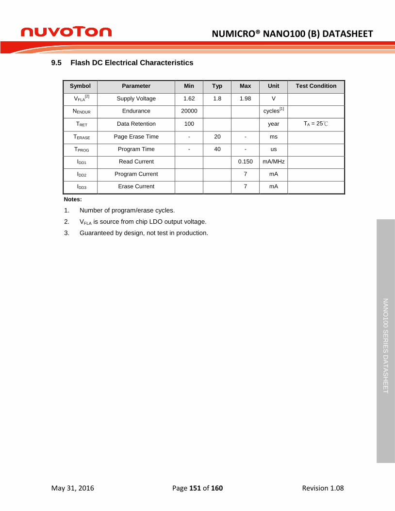
NUMICRO® NANO100 (B) DATASHEET
May 31, 2016 Page 151 of 160 Revision 1.08
NA
NO
10
0 S
ER
IES
DA
TA
SH
EE
T
9.5 Flash DC Electrical Characteristics
Symbol Parameter Min Typ Max Unit Test Condition
VFLA[2]
Supply Voltage 1.62 1.8 1.98 V
NENDUR Endurance 20000 cycles[1]
TRET Data Retention 100 year TA = 25
TERASE Page Erase Time - 20 - ms
TPROG Program Time - 40 - us
IDD1 Read Current 0.150 mA/MHz
IDD2 Program Current 7 mA
IDD3 Erase Current 7 mA
Notes:
1. Number of program/erase cycles.
2. VFLA is source from chip LDO output voltage.
3. Guaranteed by design, not test in production.

NUMICRO® NANO100 (B) DATASHEET
May 31, 2016 Page 152 of 160 Revision 1.08
NA
NO
10
0 S
ER
IES
DA
TA
SH
EE
T
10 PACKAGE DIMENSIONS
10.1 LQFP128 (14x14x1.4 mm footprint 2.0 mm)

NUMICRO® NANO100 (B) DATASHEET
May 31, 2016 Page 153 of 160 Revision 1.08
NA
NO
10
0 S
ER
IES
DA
TA
SH
EE
T
10.2 LQFP64 (10x10x1.4 mm footprint 2.0 mm)

NUMICRO® NANO100 (B) DATASHEET
May 31, 2016 Page 154 of 160 Revision 1.08
NA
NO
10
0 S
ER
IES
DA
TA
SH
EE
T
10.3 LQFP64 (7x7x1.4 mm footprint 2.0 mm)

NUMICRO® NANO100 (B) DATASHEET
May 31, 2016 Page 155 of 160 Revision 1.08
NA
NO
10
0 S
ER
IES
DA
TA
SH
EE
T

NUMICRO® NANO100 (B) DATASHEET
May 31, 2016 Page 156 of 160 Revision 1.08
NA
NO
10
0 S
ER
IES
DA
TA
SH
EE
T
10.4 LQFP48 (7x7x1.4 mm footprint 2.0 mm)

NUMICRO® NANO100 (B) DATASHEET
May 31, 2016 Page 157 of 160 Revision 1.08
NA
NO
10
0 S
ER
IES
DA
TA
SH
EE
T
10.5 QFN48 (7x7x0.85 mm)

NUMICRO® NANO100 (B) DATASHEET
May 31, 2016 Page 158 of 160 Revision 1.08
NA
NO
10
0 S
ER
IES
DA
TA
SH
EE
T
11 REVISION HISTORY
Date Revision Description
2012.10.11 1.00 Initial release
2012.12.11 1.01
1. Added SmartCard UART mode description in Pin Description.
2. Unified the abbreviation (TMR) in the Timer Controller section.
3. Modified the specifications of external input clock.
4. Added LCD COM4 and COM5 description for each pin description and diagram.
5. Updated the ADC enabled by timer event description in the ADC section.
6. Changed Timer0/1 Ch0/1 to Timer x (x=0, 1, 2, 3) in the Timer Controller section.
2012.12.17 1.02 1. Added description of reading UCID in ISP mode.
2012.12.28 1.03
1. Added R-type related description in LCD section.
2. Updated the operating current data of Run mode and Idle mode at each frequency and added related data at 42 MHz in section 9.2.
2013.01.02 1.04 1. Updated the table in Power Consumption section.
2013.03.05 1.05
1. Updated the display modes from four to six in section 5.13.2.
2. Corrected the pin descriptions in section 3.4.
3. Updated temperature sensor of analog characteristic in section 9.4.4.
4. Corrected Smart Card’s feature to be half duplex in UART mode in section 5.16.2.
2013.05.28 1.06
1. Updated the Nano110 LQFP128-pin diagram in section 3.3.2.
2. Updated “12 MHz OSC has 2 % deviation within all temperarure range” in sections 2.1 to 2.4.
3. Updated DAC analog characteristics in section 9.4.5.
4. Added Nano110RC2BN to the Nano110 LCD Line Selection Guide.
2013.12.04 1.07
1. Updated Nano100 series selection code in section 3.1.
2. Added the Nano100 QFN48 package in section 3.2 and QFN48 package dimensions in chapter 10.
3. Fixed the typo of LCD characteristic in section 9.4.7.
4. Added a note that “Output voltage for ADC/LCD shared pins cannot be higher than VDD because these pins are without 5V tolerance.” for pin description in section 3.4, LCD overview in section 5.13.1 and Absolute Maximum Ratings in section 9.1.
5. Modified the schematic for ADC and DAC application circuit in section

NUMICRO® NANO100 (B) DATASHEET
May 31, 2016 Page 159 of 160 Revision 1.08
NA
NO
10
0 S
ER
IES
DA
TA
SH
EE
T
7.2 and 7.3.
2016.05.31 1.08
1. Added Flash DC Electrical Characteristics in section 9.5.
2. Fixed the typo of LCD Feature in section 5.13.2.
3. Fixed the typo of Products Selection Guide in section 3.2
4. Modified the schematic for ADC, DAC and Whole Chip Application Circuit in section 7.2, 7.3 and 7.4.

NUMICRO® NANO100 (B) DATASHEET
May 31, 2016 Page 160 of 160 Revision 1.08
NA
NO
10
0 S
ER
IES
DA
TA
SH
EE
T
Important Notice
Nuvoton Products are neither intended nor warranted for usage in systems or equipment, any malfunction or failure of which may cause loss of human life, bodily injury or severe property damage. Such applications are deemed, “Insecure Usage”.
Insecure usage includes, but is not limited to: equipment for surgical implementation, atomic energy control instruments, airplane or spaceship instruments, the control or operation of dynamic, brake or safety systems designed for vehicular use, traffic signal instruments, all types of safety devices, and other applications intended to support or sustain life.
All Insecure Usage shall be made at customer’s risk, and in the event that third parties lay claims to Nuvoton as a result of customer’s Insecure Usage, customer shall indemnify the damages and liabilities thus incurred by Nuvoton.