
Nishad Nerurkar Aniket Mhatre - Muhammad Shaaban's...
32
- Nishad Nerurkar - Aniket Mhatre
Transcript of Nishad Nerurkar Aniket Mhatre - Muhammad Shaaban's...
- Nishad Nerurkar
- Aniket Mhatre

Single Chip Cloud Computer is a project developed by Intel.
It was developed by Intel Lab Bangalore, Intel Lab America and Intel Lab Germany.
It is part of a larger project, the Tera-scale computer which aims at executing trillions of calculations per second (teraflops).

It is a technique in which multiple calculations are performed simultaneously.
This can be achieved by dividing larger problems into smaller ones and solving them concurrently.
On a small-scale, it can be implemented using multi-core and multi-processor computers having multiple processing elements within a single machine.
On a large-scale, clusters, MPPs, and grids use multiple computers to work on highly parallel tasks concurrently.

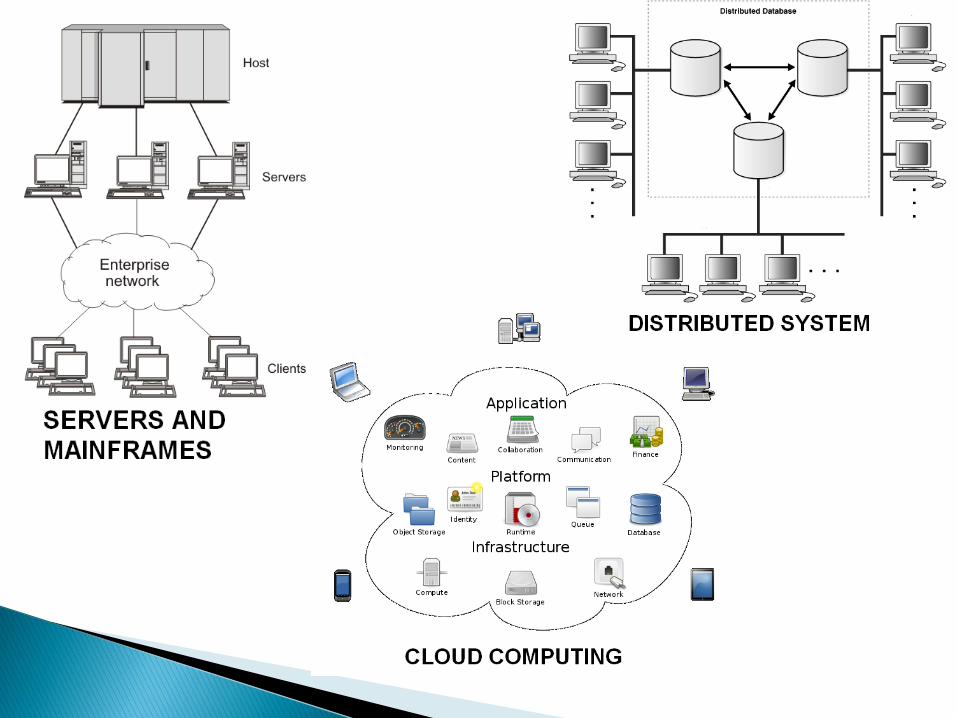
Servers and Mainframes ◦ Used in medium-scale enterprises for parallel data
access and data processing.
Distributed Systems ◦ Multiple autonomous computers that communicate
through a computer network. ◦ The computers interact with each other in order to
process data simultaneously.
Cloud Computing ◦ Higher version of distributed systems where multiple
computers are connected over the internet. ◦ Computation, software, data access, and storage
services are provided by the network.
Data centers handle and service large amount of data.
Need for low power data centers.
Need for faster parallel computing to service the requests.
At the same time reduce the power consumption for a network cloud.
Scheduling and Co-ordinating Multiple computing elements with a constraint of time and speed.
The Single Chip Cloud computer achieves the previously mentioned goals.
It is analogous to a cloud network hence the name “cloud” computer.
The SCC contains a cloud network and 48 cores along with on-chip memory and cache.
It can work as a multi-core processor as well as a fast message routing and data servicing network.
Its power consumption ranges from 25Watts to 125 Watts, which is much lower than that of the Intel i7 (156 Watts)

Processor Mode: ◦ In processor mode, the cores are operational. In this mode,
cores execute code from system memory and programmed I/O through the system interface that is connected off die to the system board FPGA.
◦ Loading memory and configuring the processor for bootstrapping is currently done by software running on the Management Console.
Mesh Mode: ◦ In mesh mode the cores are off and the router is stressed
for performance measurements. ◦ The mesh and traffic generators are on and are sending and
receiving large amounts of data. ◦ Because the core logic is off, there is no memory map. ◦ Traffic generators and routers are programmed through the
SCC JTAG interface.

Programs may be loaded into SCC memory by the Management Console through the system interface and via the SCC on-die mesh.
The memory on the SCC may be dynamically mapped to the address space of the 48 cores. It may also be mapped to the memory space of the Management Console, for program loading or debug.
I/O instructions on the SCC processor cores are also mapped to the system interface and by default to the Management Console interface. Programs on the MCPC can capture and display such programmed I/O.
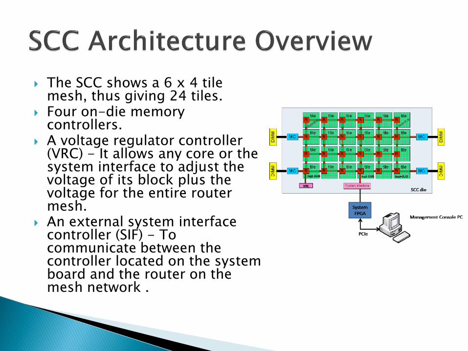
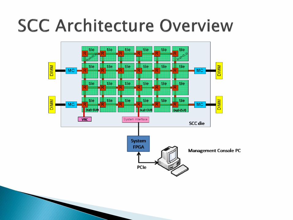
The SCC shows a 6 x 4 tile mesh, thus giving 24 tiles.
Four on-die memory controllers.
A voltage regulator controller (VRC) - It allows any core or the system interface to adjust the voltage of its block plus the voltage for the entire router mesh.
An external system interface controller (SIF) - To communicate between the controller located on the system board and the router on the mesh network .
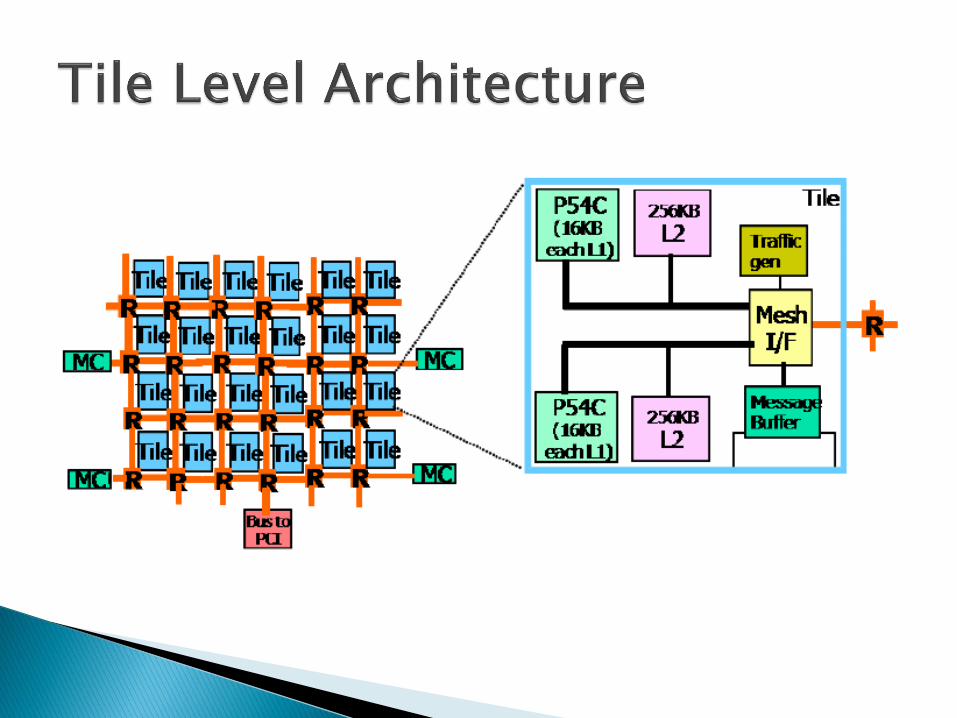
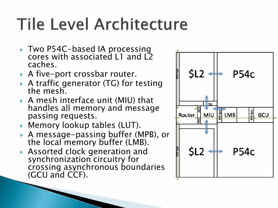
Two P54C-based IA processing cores with associated L1 and L2 caches.
A five-port crossbar router. A traffic generator (TG) for testing
the mesh. A mesh interface unit (MIU) that
handles all memory and message passing requests.
Memory lookup tables (LUT). A message-passing buffer (MPB), or
the local memory buffer (LMB). Assorted clock generation and
synchronization circuitry for crossing asynchronous boundaries (GCU and CCF).
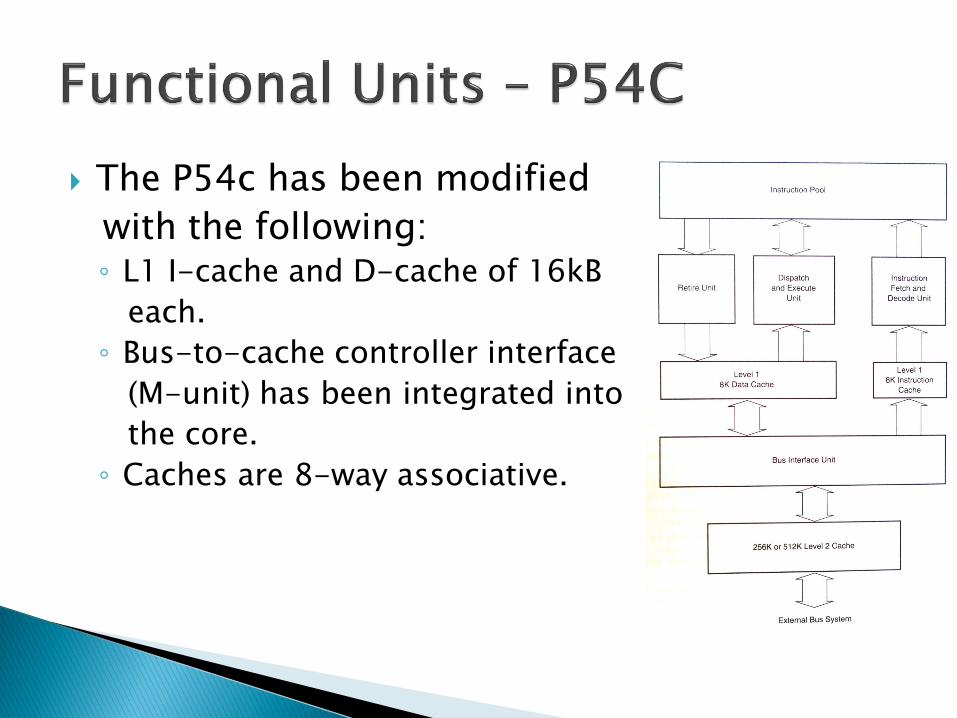
The P54c has been modified
with the following: ◦ L1 I-cache and D-cache of 16kB
each.
◦ Bus-to-cache controller interface
(M-unit) has been integrated into
the core.
◦ Caches are 8-way associative.

The P54C ISA was extended with a new instruction - (CL1INVMB) and a new memory type MPBT) to facilitate the use of message data.
All accesses to MPBT data bypass the L2 cache.
The new instruction was added to invalidate all L1 cache lines typed as MPBT. This maintains coherency between caches and message data.
A write combine buffer was added to the M-unit to accelerate the message transfer between cores.
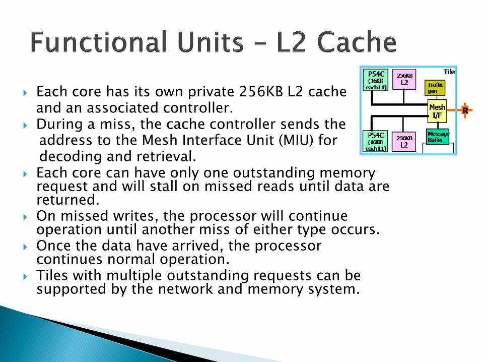
Each core has its own private 256KB L2 cache and an associated controller. During a miss, the cache controller sends the
address to the Mesh Interface Unit (MIU) for decoding and retrieval. Each core can have only one outstanding memory
request and will stall on missed reads until data are returned.
On missed writes, the processor will continue operation until another miss of either type occurs.
Once the data have arrived, the processor continues normal operation.
Tiles with multiple outstanding requests can be supported by the network and memory system.

LMB – Local Memory Buffer ◦ 16KB buffer provides the equivalent of 512 full cache lines of memory. ◦ 24 buffers on chip ◦ Capable of fast R/W operations . ◦ Any core can R/W any buffer.
DDR3 Memory Controller ◦ Four memory controllers = 64GB DDR3 memory ◦ Two unbuffered DIMMs per channel with two ranks
per DIMM. ◦ In order memory access, accesses to different
banks and ranks are interleaved
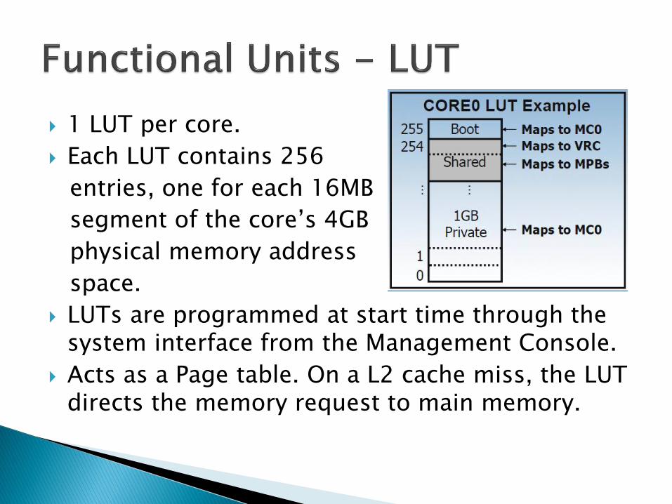
1 LUT per core.
Each LUT contains 256
entries, one for each 16MB
segment of the core’s 4GB
physical memory address
space.
LUTs are programmed at start time through the system interface from the Management Console.
Acts as a Page table. On a L2 cache miss, the LUT directs the memory request to main memory.
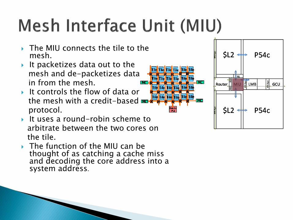
The MIU connects the tile to the mesh.
It packetizes data out to the mesh and de-packetizes data in from the mesh. It controls the flow of data on the mesh with a credit-based protocol. It uses a round-robin scheme to
arbitrate between the two cores on the tile. The function of the MIU can be
thought of as catching a cache miss and decoding the core address into a system address.
The MIU contains the following components: ◦ Packetizer and De-Packetizer: The packetizer/de-
packetizer translates the data to/from the tile agents and to/from the mesh.
◦ Command interpretation and address decode/lookup: It decodes the address using the LUTs and place the request into the queue.
◦ Local configuration registers: For traffic coming from the router, the MIU routes the data to the appropriate local destination using the registers.
◦ Link level flow control and Credit Management: It ensures flow of data on the mesh using a credit-based protocol.
◦ Arbiter: The arbiter controls tile element access to the MIU at any given time via a round robin scheme.
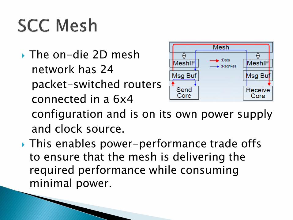
The on-die 2D mesh
network has 24
packet-switched routers
connected in a 6x4
configuration and is on its own power supply
and clock source.
This enables power-performance trade offs to ensure that the mesh is delivering the required performance while consuming minimal power.

Router (RXB): The RXB is the next generation router for future many-core 2D mesh fabrics.
The different tile agents on the mesh fabric communicate with each other.
A packet consists of a single flit or multiple flits (up to three) with header, body and tail flits. Control flits are used to communicate control
information.

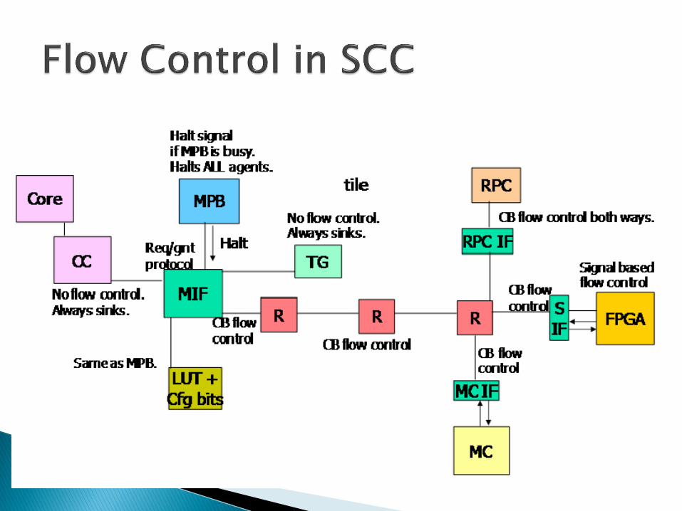
Flow control in SCC is credit-based for the routers on the mesh.
Each router has eight credits to give per port.
A router can send a packet to another router only when it has a credit from that router.
Credits are automatically routed back to the sender when the packet moves on to the next destination.
The SCC provides low level capabilities to support a variety of programming models.
The SCC also supports different configurations of the memory by using the configuration registers and lookup tables in each tile.
At any time, software has the ability to change the memory map for a core.

Each of the SCC’s four memory controllers provides access to form 4GB to 16GB of main memory (64GB).
Lookup Tables map addresses from the core physical addresses to system physical addresses.
The shared space may be used for sending data between the cores or for storing shared data such as an in-memory database.

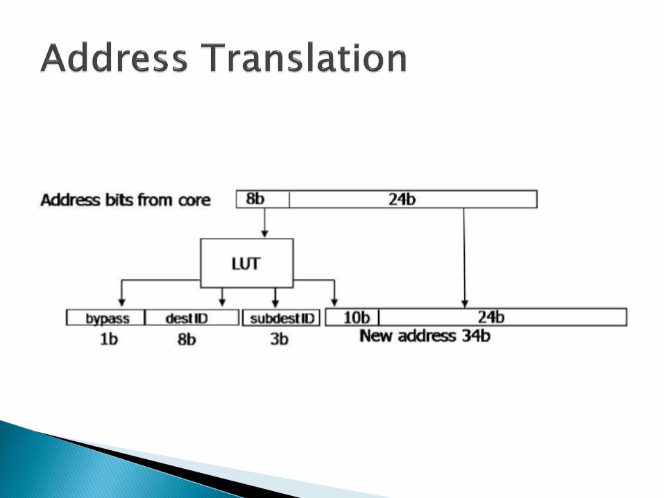
The SCC Lookup Table (LUT) unit performs the address translation from core address to system address.
The operating mode of this unit is governed by the tile level configuration registers.
Two LUTs, one for each core, are used to translate all outgoing core addresses into system addresses.
To ensure proper physical routing of system addresses, the LUTs also provide router destination IDs and intra-tile sub-IDs.
A bypass bit is also provided for local tile memory buffer access.
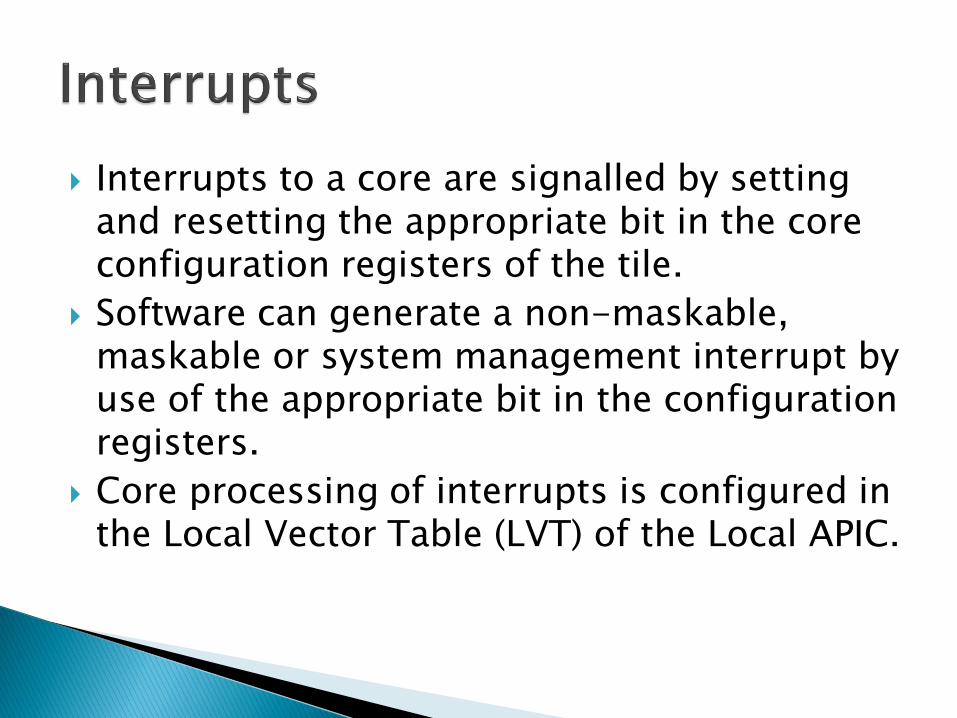
Interrupts to a core are signalled by setting and resetting the appropriate bit in the core configuration registers of the tile.
Software can generate a non-maskable, maskable or system management interrupt by use of the appropriate bit in the configuration registers.
Core processing of interrupts is configured in the Local Vector Table (LVT) of the Local APIC.

Super Computer
Computer Vision – 3D vision
Low Power Data centers
Servers
High-end Game Consoles
Building blocks of Tera-scale computers.


![Educating India: Every child in School Workshop on …...of Governors, XLRI; Fr. E Abraham, S. J. Director of XLRI and Dr. Pranabesh Ray, Dean [Academics] at XLRI. Mr. H M Nerurkar](https://static.fdocuments.us/doc/165x107/5f5400c32a0f632dd4294f6e/educating-india-every-child-in-school-workshop-on-of-governors-xlri-fr-e.jpg)


