National Institute of Technology, Tiruchirappalli ......1. Enhancing the saturation magnetisation in...
28
National Institute of Technology, Tiruchirappalli: Performa for CV of Faculty Members Dr.N.Gopalakrishnan did his Ph.D in 1997 at Anna University, Chennai, in the Nucleation and Growth kinetics of III-V Semiconductor. After his Ph.D, he went to Royal Institute of Technology, Sweden for the Post Doctoral research. Later, he had been at Japan for 3 years for Post Doctoral Research at KIT and AIST, Japan. He had been offered prestigious STA (i.e JSPS) fellowship by Japan Science and Technology, Government of Japan for his stay at AIST, Tsukuba, Japan. He had been also at South Korea for one and half years as a Post-Doctoral researcher in Dong-Eui University. Since March 2018, he is working as Professor of Physics at National Institute of Technology (NIT), Tiruchirapalli. Earlier, he joined as an Assistant Professor in Sept. 2007 and subsequently promoted to Associate Professor in Sept. 2010. He had been also served as Associate Dean (Academic) in NIT-T from Oct.2012 to Nov.2015 and Head, Department of Physics from Jan.2015-Jan.2018. Dr.N.Gopalakrishnan published about 71 research papers in the International journals and presented about 86 research papers in the National and International conferences. Under his supervision 3 students completed Ph.D degree and 36 students completed Master degree projects. Currently, 9 students are doing Ph.D under his supervision. Dr.N.Gopalakrishnan has good experience in Growth of III-V and II-VI thin films by versatile techniques, VPE, MBE, PLD and Sputtering. Beside, his group is working in synthesis of oxide nanomaterials, Spintronics, Gas sensing and Water purification. Recently, his group successfully fabricated ZnO p-n junction and CuO based sensor devices. Beside his Post Doctoral Research in Sweden, Japan and South Korea, he visited United States of America, Germany, Hong Kong, Australia, Germany and Singapore for conferences, scientific discussion, Lab visit and to deliver invited lectures. He has delivered several invited lectures in India as well as in abroad. Brief CV of Dr. N.Gopalakrishnan
Transcript of National Institute of Technology, Tiruchirappalli ......1. Enhancing the saturation magnetisation in...

National Institute of Technology, Tiruchirappalli: Performa for CV of Faculty Members
Dr.N.Gopalakrishnan did his Ph.D in 1997 at Anna University, Chennai, in the Nucleation
and Growth kinetics of III-V Semiconductor. After his Ph.D, he went to Royal Institute
of Technology, Sweden for the Post Doctoral research. Later, he had been at Japan for 3
years for Post Doctoral Research at KIT and AIST, Japan. He had been offered
prestigious STA (i.e JSPS) fellowship by Japan Science and Technology, Government of
Japan for his stay at AIST, Tsukuba, Japan. He had been also at South Korea for one and
half years as a Post-Doctoral researcher in Dong-Eui University.
Since March 2018, he is working as Professor of Physics at National Institute of
Technology (NIT), Tiruchirapalli. Earlier, he joined as an Assistant Professor in Sept. 2007
and subsequently promoted to Associate Professor in Sept. 2010. He had been also served
as Associate Dean (Academic) in NIT-T from Oct.2012 to Nov.2015 and Head, Department
of Physics from Jan.2015-Jan.2018. Dr.N.Gopalakrishnan published about 71 research
papers in the International journals and presented about 86 research papers in the National
and International conferences. Under his supervision 3 students completed Ph.D degree and
36 students completed Master degree projects. Currently, 9 students are doing Ph.D under his
supervision.
Dr.N.Gopalakrishnan has good experience in Growth of III-V and II-VI thin films by
versatile techniques, VPE, MBE, PLD and Sputtering. Beside, his group is working in
synthesis of oxide nanomaterials, Spintronics, Gas sensing and Water purification.
Recently, his group successfully fabricated ZnO p-n junction and CuO based sensor devices.
Beside his Post Doctoral Research in Sweden, Japan and South Korea, he visited United
States of America, Germany, Hong Kong, Australia, Germany and Singapore for
conferences, scientific discussion, Lab visit and to deliver invited lectures. He has delivered
several invited lectures in India as well as in abroad.
Brief CV of Dr. N.Gopalakrishnan

CV of N.Gopalakrishnan
Name : N.GOPALAKRISHNAN
Date of Birth : 9th May 1967
Nationality : Indian
Sex : Male
Martial Status : Married
Address for Communication : Dr. Nammalvar Gopalakrishnan
Professor
Department of Physics
National Institute of Technology (NIT)
Tiruchirapalli-620 006, INDIA.
E.mail: [email protected]
Mobile: (+91) 98949-14905
Education:
Ph.D (Physics) April 1997 Anna University, Chennai, India.
M.Phil (Physics) Sept.1991 Anna University, Chennai, India.
M.Sc (Physics) April.1990 M.K.University, Madurai, India.
Current Position and Administration detail:
Professor
Department of Physics
National Institute of Technology
Tiruchirappalli-15
Since 12 March 2018
Teaching and Research
Head
Department of Physics
National Institute of Technology
Tiruchirappalli-15
Jan.2015-Jan2018
Teaching, Research and
Administration
Associate Dean (Academic)
National Institute of Technology Tiruchirappalli-15
Oct. 2012 –Nov.2015
Teaching, Research and
Administration
Teaching:
Under Graduate - * Engineering Physics-I * Engineering Physics-II
Post Graduate - * Thin Film Technology * Solid State Physics
* Electrical, Magnetic and Optoelectronic Materials
* Fabrication Technology
Research: Thin films growth (Sputtering/PLD/MBE/HVPE)/
Synthesis of oxide nanostructures/ Optoelectronics/
Spintronics/ Gas sensing/ Water Purification

Research supervision:
Ph.D Supervision - 03 (completed)
09 (on going)
Master degree projects - 43 (completed)
03 (on going)
Projects ongoing/completed:
1. ‘Doping and Capping in ZnO thin films for spintronics applications’ sanctioned by
CSIR, Govt. of India (July 2014 – July 2017).
2.‘Codoping and band gap engineering in ZnO thin films for optoelectronics
applications’ sanctioned by DRDO, Govt. of India (Jan. 2009 – Jan. 2012).
Details of Professional Experiences:
Organisation Designation Period
From - To
Nature of Job
Dept. of Physics
National Inst. of Technology
Tiruchirapalli-620 015.
Dept. of Physics
National Inst. of Technology
Tiruchirapalli-620 015.
Dept. of Physics
National Inst. of Technology
Tiruchirapalli-620 015.
Dept. of Physics
National Institute of Physics
Tiruchirapalli-620 015.
Electronic Ceramic Centre
Dong-Eui University, KOREA
AIST Central-2, Tsukuba
JAPAN.
Kyoto Inst. of Tech (KIT)
JAPAN.
Royal Inst. of Tech (KTH).
SWEDEN.
Professor
Associate Professor
Assistant Professor
CSIR-Senior Research
Associate
Post Doctoral Fellow
STA Fellow
&
AIST Post Doctoral
Researcher
Post Doctoral
Researcher
Post Doctoral
Researcher
Since March
2018
Sept.2010-
March 2018
Sept.2007-
Sept. 2010
May 2006-
Sept.2007
June 2004-
August 2005
October 2000-
March 2003
Oct.1999 –
Mar 2000
May.1997 –
Jun.1998
Teaching &
Research
Teaching &
Research
Teaching &
Research
Research &
Teaching
Research
Research
Research
Research

Present work at NIT, Tiruchirapalli, India: * Teaching for Under Graduate (B.Tech) & Post Graduate (M.Sc/M.Tech) students
* Research Supervision for Doctoral & Master Students
* Responsible for Thin film laboratory (Group leader)
* Developed Thin film laboratory
* Growth of ZnO thin films by RF Sputtering for LED and Spintronics applications
* Successfully fabricated p-ZnO films.
* Successfully fabricated ZnO p-n junction.
* Synthesis of metal oxide nanostructures for Gas sensing applications.
* Fabrication of nanofillers incorporated polymer membranes for water purification.
Research at Dong-Eui University, Korea:
* Thin film growth of ZnO by Pulsed Laser Deposition (PLD) for LED application
(GaN, B2O3 and BN doped ZnO in N2O ambient by codoping and
triple codoping approach)
* Characterisation of ZnO Thin films
(Xrd, AFM, UV-VIS-NIR, PL, GDMS, Hall effect)
* ZnO Target Preparation for Ablation
(Uniaxial press, Cold Isostaic Press, Ball Milling and Sintering)
Research at AIST, Japan:
* Thin film growth of GaAs on Si by MBE for solar cells application
(Growth of GaAs and AlGaAs, Solar cell structures, Thermal Cyclic Annealing, Growth rate
check, Flux measurement etc.)
* Thickness measurement (DEKTAK profiler)
* Chemical Cleaning of GaAs and Si Substrates
* Photolumienscence studies (PL), Atomic Force Microscope (AFM)
* Xrd analysis, in situ RHEED measurement during MBE
* Optimization of new ULVAC MBE system (MBE system Baking, cell baking etc.)
* Growth of metals on GaAs
Research Expeience at KTH, Sweden & others:
* Epitaxial growth of InP:Fe by HVPE for Laser Fabrications
* Hall Measurements of epilayers.
* Reactive ion Etching (RIE), Photolithography
* Material processing, Fabrication of Mesas & Laser Characterisation
* Modelling on planar substrates for HVPE:
* Modelling on patterned substrates for HVPE:
Anisotropy behaviour of InP, around [110] and [-110] directional etched Mesas
(Effect of surface diffusion length and surface diffusion coefficient)

No. of Ph.D, M.Sc and M.Tech projects completed/ongoing
No of Ph.D. Completed (03)
No of Ph.D. ongoing ( 09)
No of Master Degree Project Completed (43)
M.Sc - 25
M.Tech - 18
Other Positions:
Organisation Designation Period
Department of Electronic Materials Engineering,
Australian National University (ANU), Canberra,
AUSTRALIA.
Institute of Nanotechnology (INT), Kharlsure
Institute of Technology (KIT), GERMANY.
Visiting Fellow
Guest Researcher
20-28 Feb.2014
24 May 2010 -
24 June 2010
Sl.No Thesis title Student name year Course
1. Realization of p-ZnO thin flms for
the fabrication of homojunction by
R.F. Magnetron sputtering. Dr.L.Balakrishnan Jan 2013 Ph D
2. Codoping and bandgap engineering
in ZnO thin films by
R.F. Magnetron sputtering. Dr.S.Gowrishankar Feb 2014 Ph D
3. Hydrothermal synthesis,
characterization and fabrication of
CuO gas sensors. Dr.S.Bhuvaneshwari July 2017 Ph.D
Sl.No Name Year of Registration
1. Mr.R.N.Lokesh August 2011
2. Mr.E.Vinoth February 2014
3. Ms.E.Hemalatha August 2014
4. Mr.N.Sivanantham February 2015
5 Ms.S.Pramila February 2015
6 Mr.Arunachalam B February 2016
7 Mr.Kirubanithy M February 2016
8 Ms.Rekha Pilliadugula August 2016
9. Ms. Arya Sukumaran July 2017
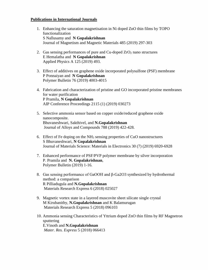
Publications in International Journals
1. Enhancing the saturation magnetisation in Ni doped ZnO thin films by TOPO
functionalization
S Nallusamy and N Gopalakrishnan
Journal of Magnetism and Magnetic Materials 485 (2019) 297-303
2. Gas sensing performances of pure and Cu-doped ZrO2 nano structures
E Hemalatha and N Gopalakrishnan
Applied Physics A 125 (2019) 493.
3. Effect of additives on graphene oxide incorporated polysulfone (PSF) membrane
P Ponnaiyan and N Gopalakrishnan
Polymer Bulletin 76 (2019) 4003-4015
4. Fabrication and characterization of pristine and GO incorporated pristine membranes
for water purification
P Pramila, N Gopalakrishnan
AIP Conference Proceedings 2115 (1) (2019) 030273
5. Selective ammonia sensor based on copper oxide/reduced graphene oxide
nanocomposite.
Bhuvaneshwari, Sakthivel, and N.Gopalakrishnan
Journal of Alloys and Compounds 788 (2019) 422-428.
6. Effect of Fe doping on the NH3 sensing properties of CuO nanostructures
S Bhuvaneshwari, N Gopalakrishnan
Journal of Materials Science: Materials in Electronics 30 (7) (2019) 6920-6928
7. Enhanced performance of PSF/PVP polymer membrane by silver incorporation
P. Pramila and N. Gopalakrishnan,
Polymer Bulletin (2019) 1-16.
8. Gas sensing performance of GaOOH and β-Ga2O3 synthesized by hydrothermal
method: a comparison
R Pilliadugula and N.Gopalakrishnan
Materials Research Express 6 (2018) 025027
9. Magnetic vortex state in a layered muscovite sheet silicate single crystal
M Kirubanithy, N.Gopalakrishnan and K Balamurugan
Materials Research Express 5 (2018) 096103
10. Ammonia sensing Characteristics of Yttrium doped ZnO thin films by RF Magnetron
sputtering
E.Vinoth and N.Gopalakrishnan
Mater. Res. Express 5 (2018) 066413
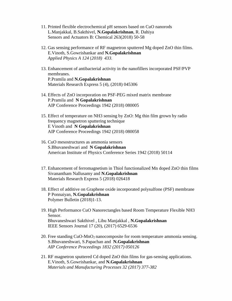
11. Printed flexible electrochemical pH sensors based on CuO nanorods
L.Manjakkal, B.Sakthivel, N.Gopalakrishnan, R. Dahiya
Sensors and Actuators B: Chemical 263(2018) 50-58
12. Gas sensing performance of RF magnetron sputtered Mg doped ZnO thin films.
E.Vinoth, S.Gowrishankar and N.Gopalakrishnan
Applied Physics A 124 (2018) 433.
13. Enhancement of antibacterial activity in the nanofillers incorporated PSF/PVP
membranes.
P.Pramila and N.Gopalakrishnan
Materials Research Express 5 (4), (2018) 045306
14. Effects of ZnO incorporation on PSF-PEG mixed matrix membrane
P.Pramila and N Gopalakrishnan
AIP Conference Proceedings 1942 (2018) 080005
15. Effect of temperature on NH3 sensing by ZnO: Mg thin film grown by radio
frequency magnetron sputtering technique
E Vinoth and N Gopalakrishnan
AIP Conference Proceedings 1942 (2018) 080058
16. CuO mesostructures as ammonia sensors
S.Bhuvaneshwari and N Gopalakrishnan
American Institute of Physics Conference Series 1942 (2018) 50114
17. Enhancement of ferromagnetism in Thiol functionalized Mn doped ZnO thin films
Sivanantham Nallusamy and N.Gopalakrishnan
Materials Research Express 5 (2018) 026418
18. Effect of additive on Graphene oxide incorporated polysulfone (PSF) membrane
P Ponnaiyan, N.Gopalakrishnan
Polymer Bulletin (2018)1-13.
19. High Performance CuO Nanorectangles based Room Temperature Flexible NH3
Sensor.
Bhuvaneshwari Sakthivel , Libu Manjakkal , N.Gopalakrishnan
IEEE Sensors Journal 17 (20), (2017) 6529-6536
20. Free standing CuO-MnO2 nanocomposite for room temperature ammonia sensing.
S.Bhuvaneshwari, S.Papachan and N.Gopalakrishnan
AIP Conference Proceedings 1832 (2017) 050126
21. RF magnetron sputtered Cd doped ZnO thin films for gas-sensing applications.
E.Vinoth, S.Gowrishankar, and N.Gopalakrishnan
Materials and Manufacturing Processes 32 (2017) 377-382

22. Fabrication of Thiol Functionalized Ni doped ZnO Thin Films for Room
Temperature Ferromagnetism.
Sivanantham Nallusamy and N.Gopalakrishnan
IEEE Magnetics Letters 8, (2017) 2109304
23. Hydrothermally synthesized Copper Oxide (CuO) superstructures for ammonia
sensing.
Bhuvaneshwari, S., and N. Gopalakrishnan.
Journal of Colloid and Interface Science 480 (2016) 76–84.
24. Room temperature ammonia and VOC sensing properties of CuO nanorods.
Bhuvaneshwari, S., and N. Gopalakrishnan
AIP Conf. Proc. 1731 (2016) 050112
25. Facile synthesis of low dimensional CuO nanostructures and their gas sensing
applications.
Bhuvaneshwari, S., and N. Gopalakrishnan.
Crystal Research and Technology 51 (2016) 145–153.
26. Enhanced ammonia sensing characteristics of Cr doped CuO nanoboats.
Bhuvaneshwari, S., and N. Gopalakrishnan.
Journal of Alloys and Compounds 654 (2016) 202-208.
27. Optimization of CuO Ultra Thin Film for Gas Sensor Application by RF Magnetron
Sputtering
N.Gopalakrishnan, L.Balakrishnan, B. Arunkumar and S. Gowrishankar
Journal of Nanoelectronics and Optoelectronics 9 (2014) 496-501.
28. A Comparative Study on p-ZnO:AlAs/n-ZnO:Al and p-ZnO:AlAsN/n-ZnO:Al
Bilayer Homojunction Diodes Performance
. L. Balakrishnan, S.Gowrishankar, and N. Gopalakrishnan
ECS Solid State Letters 3 (2014) Q20-Q23
29. Role of surface functionalization in ZnO:Fe nanostructures
R.N. Lokesh, L. Balakrishnan, K. Jeganathan, Samar Layek, H.C. Verma,
N. Gopalakrishnan
Materials Science and Engineering B 183 (2014) 39– 46.
30. Bandgap engineering in Zn(1-x)CdxO and Zn(1-x)MgxO thin films by RF Sputtering.
S. Gowrishankar, L. Balakrishnan and N. Gopalakrishnan
Ceramics International 40 (2014) 2135-2142.
31. Hydrothermal Synthesis and Gas Sensing Properties of CuO Nanorods
N. Gopalakrishnan, S. Bhuvaneshwari, L.Balakrishnan and S.Gowrishankar
Sensor letters 11 (2013) 2233-2240.

32. Fabrication of p-ZnO:ZrN thin films by RF magnetron sputtering.
S. Gowrishankar, L. Balakrishnan and N. Gopalakrishnan
Composite Interfaces 20 (2013) 623-634.
33. p-type formation mechanism of codoped and tridoped ZnO thin films.
L. Balakrishnan, S.R. Barman and N. Gopalakrishnan
Science of Advanced Materials 5 (2013) 462-468.
34. Fabrication of n-Zn1-xGaxO and p-(ZnO)1-x(GaP)x thin films and homojunction.
S. Gowrishankar, L. Balakrishnan, T. Balasubramanian and N. Gopalakrishnan
Materials Science and Engineering B 178 (2013) 31– 38.
35. Activation of room temperature ferromagnetism in ZnO films by surface
functionalization with thiol and amine
G. Jayalakshmi, N. Gopalakrishnan, T. Balasubramanian
Journal of Alloys and Compounds 551 (2013) 667-671.
36. NH3 sensing by p-ZnO thin films.
L. Balakrishnan, S. Gowrishankar and N. Gopalakrishnan
IEEE Sensors Journal 13 (2013) 2055-2060.
37. Influence of oxygen partial pressure on ferromagnetic switching characteristics of
ZnO:Cr thin films.
N. Gopalakrishnan, L. Balakrishnan, M. Suganya and S. Gowrishankar
Composite Interfaces 20 (2013) 221-228.
38. Fabrication of tridoped p-ZnO thin film and homojunction by RF magnetron
sputtering.
L. Balakrishnan, S. Gowrishankar and N. Gopalakrishnan
Ceramics International 38 (2012) 6221–6227.
39. Fabrication of Al3+ and large radii mismatch As5+ codoped p-ZnO thin film and
homojunction.
L. Balakrishnan and N. Gopalakrishnan
Thin Solid Films 520 (2012) 5702–5705.
40. Dual codoping for the fabrication of low resistive p-ZnO
L. Balakrishnan, S. Gowrishankar, P. Premchander and N. Gopalakrishnan
Journal of Alloys and Compounds 512 (2012) 235– 240.
41. Thickness and substrate orientation dependence of ferromagnetism in Mn doped ZnO
thin films
N. Gopalakrishnan, L. Balakrishnan, A. Brindha and G. Jayalakshmi
Cryst. Res. Technol., 47 (2012) 45-52.
42. Optimization of Anodic Layer and Fabrication of Organic Light Emitting Diode.
N. Gopalakrishnan, S. Gowrishankar, T. R. Devidas and L. Balakrishnan
Advanced Materials Research 488-489 (2012) 1348-1352.

43. Influence of Al concentration on electrical, structural and optical properties
of Al–As codoped p-ZnO thin films
L. Balakrishnan, S. Gowrishankar, J. Elanchezhiyan, N. Gopalakrishnan
Physica B 406 (2011) 4447 –4452.
44. Grain boundary defects induced room temperature ferromagnetism in V doped ZnO
thin films
G. Jayalakshmi, N. Gopalakrishnan, B.K. Panigrahi, T. Balasubramanian
Crystal Research and Technology 46 (2011) 1257-1264
45. Realization of p-ZnO thin films by GaP codoping
S. Gowrishankar, L. Balakrishnan, J. Elanchezhiyan, T. Balasubramanian,
N. Gopalakrishnan,
Physica B 406 (2011) 4085–4088.
46. Influence of substrate and film thickness on structural, optical
and electrical properties of ZnO thin films
N. Gopalakrishnan, L. Balakrishnan, K. Latha, and S. Gowrishankar
Cryst. Res. Technol.46 (2011) 361-367.
47. AlN codoping and fabrication of ZnO homojunction by RF sputtering
L. Balakrishnan, P. Premchander, T. Balasubramanian, N. Gopalakrishnan
Vacuum 85 (2011) 881-886.
48. Influence of grain size on the properties of AlN doped ZnO thin film
K.P. Bhuvana, J. Elanchezhiyan, N. Gopalakrishnan, T. Balasubramanian
Materials Science in Semiconductor Processing 14 (2011) 84-88.
49. Characterization of (ZnO)1-x(AlN)x/ZnO junction for optoelectronic applications
N. Gopalakrishnan, L. Balakrishnan, V. Senthamizh Pavai, J. Elanchezhiyan,
T. Balasubramanian
Current Applied Physics 11 (2011) 834-837.
50. Influences of thermal annealing on the stuctural, optical and electrical properties of
nanostructured cadmium sulphide thin films
G. Bakiyaraj, N. Gopalakrishnan and R. Dhanasekaran
Chalcogenide Letters 8 (2011) 419-426.
51. Vacancy mediated room temperature ferromagnetism in Zn1-xMnxO thin films
N. Gopalakrishnan, L. Balakrishnan, B. Srimathy, M. Senthil Kumar and
T. Balasubramanian
Physics Status Solidi A 207 (2010) 2180–2184.
52. Nucleation and characterization of Zn1-xMnxO thin films deposited on different
substrates
N. Gopalakrishnan, J. Elanchezhiyan, K.P. Bhuvana and T. Balasubramanian
Physica B: Condensed Matter 404 (2009) 1563-1567.

53. Investigations of the properties of Zn1−xCrxO thin films grown by RF magnetron
sputtering
J. Elanchezhiyan, K.P. Bhuvana, N. Gopalakrishnan, B.C. Shin, W.J. Lee,
T. Balasubramanian
Journal of Alloys and Compounds 478 (2009) 45-48.
54. A novel approach for codoping in ZnO by AlN
K.P. Bhuvana, J. Elanchezhiyan, N. Gopalakrishnan, B.C. Shin, W.J. Lee,
T. Balasubramanian
Vacuum 83 (2009) 1081-1085.
55. Realization of p-type conduction in (ZnO)1-x(AlN)x thin films grown by RF magnetro
n sputtering
K.P. Bhuvana J. Elanchezhiyan, N. Gopalakrishnan and T. Balasubramanian
Journal of Alloys and Compounds 478 (2009) 54-58.
56. Realization of room temperature ferromagnetism in Zn1−xCrxO thin films grown by
RF magnetron sputtering
J.Elanchezhiyan, K.P. Bhuvana, N. Gopalakrishnan, Yong Chang, S. Sivananthan,
M. Senthil Kumar and T. Balasubramanian
Journal of Alloys and Compounds 468 (2009) 7–10
57. Optimization of Zn1-xAlxO film for antireflection coating by R.F. sputtering
K.P. Bhuvana J. Elanchezhiyan, N. Gopalakrishnan and T. Balasubramanian
J. of Alloys and Compounds 473(2009) 534-537.
58. Codoped (AlN) and monodoped (Al) ZnO thin films grown by R.F. Sputtering; A
comparative study
K.P. Bhuvana J. Elanchezhiyan, N. Gopalakrishnan and T. Balasubramanian
Applied Surface Science 255 (2008) 2026–2029
59. On the nucleation and growth of Zn1-xMnxO thin films grown by RF magnetron sputte
ring
N.Gopalakrishnan, J. Elanchezhiyan, K.P. Bhuvana and T. Balasubramanian
Scripta Materialia. 58 (2008) 930-933
60. Fabrication of GaN doped ZnO nanocrystallines by Laser ablation
N. Gopalakrishnan, B.C. Shin, K.P. Bhuvana, J. Elanchezhiyan and T.
Balasubramanian
J. of Nanoscience and Nanotechnology 8 (2008) 4168-4171.
61. Improvement of stoichiometry in (ZnO)1-x(GaN)x thin films grown by Laser ablation
N. Gopalakrishnan, B.C. Shin, K.P. Bhuvana, J. Elanchezhiyan and T.
Balasubramanian
J. of Alloys and Compounds 465 (2008) 502-505.
62. Effect of doping concentration on Zn1-xMnxO thin films grown by RF magnetron
sputtering
J. Elanchezhiyan, K.P. Bhuvana, N. Gopalakrishnan and T. Balasubramanian
Z. Naturforsch 63 a (2008) 585-590.
63. Investigation on Mn doped ZnO epitaxial films grown by RF magnetron sputtering
J. Elanchezhiyan, K.P. Bhuvana, N. Gopalakrishnan and T. Balasubramanian
Materials Letters 62 (2008) 3379-3381.
64. Substrates effect on Zn1-xMnxO thin films grown by RF magnetron sputtering
J. Elanchezhiyan, K.P. Bhuvana, N. Gopalakrishnan and T. Balasubramanian
J. of Alloys and Compounds 463(2008) 84-88.
65. Influence of post-deposition annealing on the structural and optical properties of ZnO
thin films prepared by sol–gel and spin-coating method.
G. Srinivasan, N. Gopalakrishnan, Y.S. Yu, R. Kesavamoorthy and J. Kumar
Superlattices and Microstructures 43(2008) 112-119.
66. Development of NLO tunable band gap organic devices for optoelectronic applications
B. K. Periyasamy, Robinson S. Jebas, N. Gopalakrishnan, T.Balasubramanian
Materials Letters 61(2007)4246-4249.
67. An attempt on triple doping in ZnO by pulsed laser deposition
N. Gopalakrishnan, B.C. Shin and T. Balasubramanian
Materials Letters 61 (2007) 4420-4422.
68. Effect of GaN doping on ZnO films by pulsed laser deposition
N. Gopalakrishnan, B.C. Shin, H.S. Lim, T. Balasubramanian and Y.S. Yu
Materials Letters 61 (2007)2307-2310.
69. Codoping in ZnO using GaN by pulsed laser deposition
N. Gopalakrishnan, B.C. Shin, H.S. Lim, T. Balasubramanian and Y.S. Yu
Journal of Crystal Growth 294(2006)273-277.
70. Comparison of ZnO:GaN films on Si(111) and Si(100) substrates by pulsed
laser deposition
N. Gopalakrishnan, B.C. Shin, H.S. Lim, G.Y. Kim and Y.S. Yu.
Physica B 376-377 (2006) 756-759.
71. Effect of low temperature grown buffer layer thickness on the growth of GaAs on
Si by MBE.
N. Gopalakrishnan, K. Baskar, H. Kawanami and I. Sakata
Journal of Crystal Growth 250(1-2)(2003)29-33.

72. Rapid epitaxial growth of conducting and insulating III-V compounds on (001),
(110), (111)A, (311)A and (311)B surfaces by HVPE.
S. Lourdudoss, N. Gopalakrishnan, H. Holtz, M. Deschler and R. Beccard
Metallurgical and Materials Transactions A, 30A (1999)1047-1051
73. Self consistent model for InP selective regrowth by Hydride Vapour Phase epitaxy.
N. Gopalakrishnan , E.R. Messmer and S. Lourdudoss
Japanese Journal of Applied Physics, 38 (1999) 1037-1039
74. Investigations on the nucleation kinetics of L-Arginen Phosphate single crystals.
P. Mohankumar, N. Gopalakrishnan, R. Jayavel and P. Ramasamy
Crystal Research Technology 34(1999)1265-1268.
75. Compositional analysis on quaternary GaxIn1-xAsyP1-y vapour phase epitaxy: A
comparison between theory and experiment.
N. Gopalakrishnan, R. Dhanasekaran and S. Lourdudoss
Materials Chemistry and Physics 50(1997) 70-75.
76. Thermodynamic analysis of GaAs1-xPx vapour phase epitaxy
N. Gopalakrishnan and R. Dhanasekaran
J.of Electrochemical Soc., 143 (1996) 2631-2635.
77. On the nucleation and composition analysis of InAs1-xPx vapour phase
epitaxial growth
N. Gopalakrishnan and R. Dhanasekaran
J. Crystal Growth 162(1996)113-120.
78. Epitaxial nucleation and growth mechanism of III-V compound semiconductors.
N. Gopalakrishnan, R.S. Qhalid Fareed and R. Dhanasekaran
J. of Indian Institute of Sciences 76 (1996) 15-21.
79. Evaluation of composition and growth rate of GaxIn1-xP vapour phase epitaxy
N. Gopalakrishnan and R. Dhanasekaran
Materials Chemistry and Physics 45 (1995) 15-21.
80. Investigations on the two dimensional nucleation and growth kinetics of InP vapour
phase epitaxy.
N. Gopalakrishnan, R. Dhanasekaran and P. Ramasamy
J. Crystal Growth 137 (1994) 235-239.
81. Vibrational transition probability and dissociation energy data for AsN molecule
N. Rajamanickam, R.N. Senthilkumar, S. Ganesan, N. Gopalakrishnan,
J. Rajkumar, V. Jegadesan and C. Dhandapani.
Acta Physica Hungarica 70 (1991) 71-76.

No of P.G (M.Sc) Projects Completed (25)
Sl.
No
PG Project title Name and year Course
1. Surface Modification of RF sputtered NiO thin
films by Ag and GO for NH3 Sensing
Kavyakala C
May 2019
M.Sc
2. Fabrication of p-ZnO:Ag/n-ZnO homojunction
by RF Magnetron Sputtering
A Muhil
May 2019
M.Sc
3. Synthesis and Characterization of n-Type ZnSe
and conversion to p- type by doping
Aashna Praveen
May 2018
M.Sc
4. Enhancement of Ferromagnetism in Vanadium
doped ZnO thin films by Thiol functionalization
Shivam Kumar
May 2018
M.Sc
5.
a. 1
Synthesis and Characterization of ZnSe by
Hydrothermal and Solvothermal Methods.
Lakshmi Harikumar
May 2017
M.Sc
6. Growth of Cr doped ZnO Thin films by R.F
Sputtering and Surface functionalization for
Spintronics Application
R.Varsha
May 2017
M.Sc
7. Enhancement of room temperature
ferromagnetism in Mn doped ZnO thin film by
RF Magnetron sputtering
Shana C P
May 2016.
M.Sc
8. Synthesis of CuO nanoparticles and CuO-MnO2
Nanocomposite for gas sensing applications
Seethal Pappachan
May 2016
M.Sc
9. Effect of Buffer layer thickness for solar cell
applications
K.Vivekanandhan
May 2015
M.Sc
10. Synthesis of ZnO, CuO Nanostructures and
ZnO-CuO Nanocomposites for Gas sensing
applications
Naga Karthick K
May 2015
M.Sc
11. Fabrication of thin film hetero-junction for solar
cell applications
Seena Mathew
May 2014
M.Sc
12. Magnesium doped Aluminum Nitride for
spintronics application
Ranjith Kumar.P
May 2014
M.Sc
13. Synthesis and characterization of perovskite
type lafeo3 multiferroics
R.Prasanna perumal
May 2013
M.Sc
14. Synthesis of Al doped ZnO for solar cell
applications
R.Ramamoorthy
May 2013
M.Sc
15. Synthesis of CuO nanorods for gas sensing
applications
S.Bhuvaneshwari
May 2012
M.Sc
16. Substrate and thickness dependence of
ferromagnetism in Mn doped ZnO films grown
by RF magnetron sputtering
A.Brindha
May 2011
M.Sc
17. Fabrication of p-CuO/n-ZnO Hetrojunction for
Gas Sensing Applications
Arunkumar.B
May 2011
M.Sc
18. Role of oxygen vacancies on Zn1-xCrxO thin
films grown by RF sputtering
M.Suganya
May 2010
M.Sc
19. Fabrication and Characterization of OLED Devidas T.R
May 2010
M.Sc
20. Effect of Substrate and Thickness on ZnO Thin
Films Grown by RF Magnetron Sputtering
K.Latha
May 2009
M.Sc
21. Fabrication of p-n Junction Using Zinc Oxide by
RF Magnetron Sputtering
V.Senthamizh Pavai
May 2009
M.Sc
22. Growth and characterization of Al doped ZnO
(AZO) thin film by R.F. Magnetron sputtering
S.Gowrishankar
May 2008
M.Sc

No of P.G (M.Tech) Projects Completed (17)
Sl.No Project title Name and year Course
1. Inspection of Longitudinal weld in Pipe and
circumferential welds by time of flight
diffraction technique (TOFD)
Vignesh K
May 2019
M.Tech
Inspection of Longitudinal weld in Pipe and
circumferential welds by time of flight
diffraction technique (TOFD)
Vignesh K
December 2018
M.Tech
2. Guided wave ultrasonic testing for the rods
of coke oven battery
Joydwipkarmakar
May 2018
M.Tech
Guided wave ultrasonic testing for the rods
of coke oven battery
Joydwipkarmakar
December 2017
M.Tech
3. 1 Defect Characterisation in Magnesium Alloy
(AZ31) plate using Pulsed Thermography.
Pramesh Vikram
May 2017
M.Tech
Defect Analysis of Butt welded joint of
structural Steel (IS-2062), Stainless Steel
(SAE-304) and STBW T91 alloy using
immersion Ultrasonic Testing.
Pramesh Vikram
December 2016
M.Tech
4. 2 Development and Validation of UT-RAY
Tracing software for flat and curved surface.
Rohit Kumar
Agrawal
May 2017
M.Tech
Effect of Radiographyc Parameters on image
quality tools in digital Radiography.
Rohit Kumar
Agrawal
December 2016
M.Tech
5. Defect size measurement using Radiographic
technique, A comparison with time of flight
diffraction method.
Manas Mishra
May 2016
M.Tech
Advanced Ultasonic ray trace. Manas Mishra
December 2015
M.Tech
23. Structural and optical properties of Al doped
ZnO thin films prepared by R.F magnetron
sputtering
J.Kabilan
May 2008
M.Sc
24. Fabrication of Al doped ZnO (AZO) films by
thermal evaporation
B.Chandrababu
May 2007
M.Sc
25. Growth and characterization of Al doped ZnO
(AZO) thin films by thermal evaporation
K.Ananth
May 2007
M.Sc

6. Electromagnetic Non-Destructive Evaluation
of Residual Stress in Shot Peened Low
Carbon Steel Subjected to fatigue.
Subhash Koner
May 2015
M.Tech
Evaluation of Residual Stress and High
Cycle Fatigue in Low Carbon Steel through
Electromagnetic Non-Destructive
Techniques.
Subhash Koner
December 2014
M.Tech
7. Multi frequency approach for accurate
thickness measurement of steam generator
tubes at grooves using remote field eddy
current technique.
Manu Josheph
May 2015
M.Tech
Development and Sensitivity Assessment of
Multi-frequency Remote field Eddy Current
Technique.
Manu Josheph
May 2014
M.Tech
8. Study of post weld heat treatment effect on
magnetic and microstructural behavior of
9Cr-1Mo steel weldment
Shaik shahazad
May 2014
M.Tech
Modeling of magnetic surface probe using
JMAG software and application of magnetic
methods for characterization of boiler tubes
Shaik shahazad
Dec. 2013
M.Tech
9. Characterization of thermal barrier coating
speicamen using thermography technique
Nidheeshkumar.B
May 2013
M.Tech
Characterization of thermal barrier coating
specimen using thermography technique
Nidheeshkumar.B
Dec. 2012
M.Tech
10. Detection and quantification of defects in
concrete structures using digital x-ray
radiography
Sajith S.G.
May 2012
M.Tech
11. Detection and quantification of defects in
concrete structures using digital x-ray
radiography
Sajitha S.G.
Dec. 2011
M.Tech
12. Deftect detection in concrete blocks using
impact –echo technique
Chandramouli
Patoju
May 2011
M.Tech
Defect detection in concrete blocks using
impact –echo technique
Chandramouli
Patoju
Dec.2010
M.Tech
13. Transmittance characdteristics and
amplification of acoustic emission siganls
during tensile deformation of mild steel
Shiva krishna L
May 2010
M.Tech
Transfer function characteristics of acoustic
emission during tensile deformation of mild
steel
Shiva krishan. L
Dec.2009
M.Tech

14. Opitmization of ground penetrating radar
system parameters for nondestructive
detection of rebars in concrete structures
(Phase –I & phase II)
Shareef Shaik
Dec. 2009 &
May 2010
M.Tech
15. Characterisation of solution annealing
behaviour of modified 9Cr-1Mo steel by
magnetic nde techniques
Jagannadham
Parikala
May 2011
M.Tech
Characterization of microstucture of
mod.9Cr-1Mo steell using magnetic
Barkhausen emission technique
Jagannadham
Parikala
Dec 2010
M.Tech
16. Higher order guided waves : an optimization
study (Phase –I & phase II)
Venkataro Burri
Dec. 2008 &
May 2009
M.Tech
17. Magnetostrictstive sensor for structural
health monitoring of plate like structures
Jojalah Gundiga
May 2009
M.Tech
Generating and detecting guided waves in
platet like structures using magnetostrictive
sensor
Jojalah Gundiga
Dec 2008
M.Tech

Conference Publications
Papers Published /Presented/ Participated in the International Conferences
1. Fabrication and characterization of pristine and GO incorporated pristine membranes
for water purification
P Pramila, N Gopalakrishnan
AIP Conference Proceedings 2115 (1), 030273
2. Enhancement of Ferromagnetism in Amine functionalized Mn doped ZnO thinfilm
Sivanantham Nallusamy, Gopalakrishnan Nammalvar
International Conference on MAGnetic Materials and Applications (ICMAGMA)
NISER, Bhuvaneswar, India during 09 -13 December 2018.
3. Thiol functionalized V doped ZnO films for Magnetic storage device Application
Sivanantham Nallusamy and Gopalakrishnan Nammalvar
International Conference on Sustainable Energy Technologies (i-SET 2018) held at
Bharathidasan University, Tiruchirappalli , India during 27-28 June 2018.
4. Y3+ incorporated ZnO thin film grown by RF magnetron sputtering for
optoelectronic applications.
E. Vinothand and N. Gopalakrishnan
International Conference on Sustainable Energy Technologies (i-SET 2018) held
at Bharathidasan University, Tiruchirappalli, India during 27-28 June 2018.
5. Organic Ligands Induced Ferromagnetism in Ni doped ZnO films
Sivanantham Nallusamy and Gopalakrishnan Nammalvar
Intermag 2018 held at Marina Bay Sands Convention Center, Singapore during
April 23-27, 2018.
6. Thiol Functionalied Cr doped ZnO films for enhanced ferromagnetism
Gopalakrishnan Nammalvar, Sivanantham Nallusamy and Varsha Ravichandran
4th International Conference on Nano Science and Nanotechnology (ICONN 2017)
held at SRM University, Chennai, during 9-11 August 2017
7. Fabrication of Thiol functionalized Ni doped ZnO thin films
Sivanantham Nallusamy and N. Gopalakrishnan,
2017-IEEE Magnetics summer school, Santander, Spain, July19-23,2017
8. Antibacterial Study on GO incorporated PSF/PVP Mixed matrix membrane for
Water Purification,
Pramila P and N. Gopalakrishnan
International Conference on Nano for Energy and Water 2017 and Indo-French
Workshop on Water Networking, University of Petroleum and Energy Studies,
Dehradun, India, Feb 22-24, 2017.
9. Enhancement of ferromagnetism in Thiol functionalized Mn doped ZnO thin films,
N. Sivanantham and N. Gopalakrishnan,
International Conference on Magnetic Materials and Applications, DMRL and
Magnetic Society of India, Hyderabad, Feb 01-03, 2017
10. Metal Oxide Semiconductors for Gas Sensing Application
Vinoth RAJ, Bhuvaneshwari S, Gopalakrishnan Nammalvar
ICEM16-A-0916, Suntec Singapore,
04th to 08th July, 2016.
11. Synthesis and Characterisation of ZnO Hierarchical Nanoflowers, Multi-linked and
High Aspect Nanorods (ICMAT13-A-2150)
R.N. Lokesh, L. Balakrishnan, K. Jeganathan and N. Gopalakrishnan
7thInternational Conference on Materials for Advanced Technologies, Suntec
Singapore,
30 June -5 July 2013
12. Synthesis and Gas Sensing Properties of CuO Nanorods (ICMAT13-A-2168 )
N. Gopalakrishnan, S. Bhuvaneshwari andL. Balakrishnan.
7th International Conference on Materials for Advanced Technologies, Suntec
Singapore,
30 June -5 July 2013
13. Optimization of anodic layer and fabrication of organic light emitting diode.
N. Gopalakrishnan, S. Gowrishankar, T.R. Devidas and L. Balakrishnan
2nd International Conference on Key Engineering Materials (ICKEM 2012),
Singapore, February 2012.
Advanced Materials Research, Vols. 488-489 (2012) 1348-1352
14. Fabrication of p-ZnO thin films by ZrNcodoping.
S. Gowrishankar, L. Balakrishnan and N. Gopalakrishnan
SPIE Optics+Photonics 2012, San Diego, USA, August 2012
Proceedings of SPIE, Vol. 8484(2012) 84840W-1-84840W-6.
15. Fabrication of ZnOhomojunction by Al-As-N tridoping.
L. Balakrishnan, S. Gowrishankar and N. Gopalakrishnan
International Semiconductor Device Research Symposium 2011 (ISDRS 2011),
University of Maryland, Maryland, USA, December 2011(IEEE Xplore). DOI: 10.1109/ISDRS.2011.6135234
16. Realization of n-ZnO:Ga/p-ZnO:GaPhomojunction by RF magnetron sputtering.
S. Gowrishankar, L. Balakrishnan, T. Balasubramanian and N. Gopalakrishnan
International Semiconductor Device Research Symposium 2011 (ISDRS 2011),
University of Maryland, Maryland, USA, December 2011(IEEE Xplore). DOI: 10.1109/ISDRS.2011.6135308
17. Effects of oxygen partial pressure on Zn0.95Cr0.05O thin films grown by RF sputtering.
N. Gopalakrishnan, L. Balakrishnan, M. Suganya, S. Gowrishankar and G.
Jayalakshmi
International Conference on Nanoscience and Nanotechnology (ICNN 2011),
Coimbatore Institute of Technology, Coimbatore, India, July 2011.
18. Dual codoping for the fabrication of low resistive p-ZnO.
L. Balakrishnan, S. Gowrishankar, J. Elanchezhiyan, B.C. Shin, T. Balasubramanian
and N. Gopalakrishnan
The 16th International Conference on Crystal Growth (ICCG-16),
Chinese Academy of Sciences, Beijing, China, August 2010.
19. Fabrication of p-n junction with ZnO nanostructures by a novel approach.
L. Balakrishnan, S. Gowrishankar, T. Balasubramanian and N. Gopalakrishnan
International Conference on “Synthesis, Characterization Consolidation and
Modelling of Nanomaterials” (ICON-2010), PSG College of Technology,
Coimbatore, March 2010.
20. Vacancy mediated ferromagnetism in Zn0.85Mn0.15O nanostructures.
L. Balakrishnan, G. Jayalakshmi, B. Srimathy, M. Senthilkumar, T. Balasubramanian
and N. Gopalakrishnan
International Conference on “Synthesis, Characterization Consolidation and
Modelling of Nanomaterials” (ICON-2010), PSG College of Technology,
Coimbatore, March 2010.
21. Dual codoping for the fabrication of low resistive p-ZnO
L.Balakrishnan, S.Gowrishankar, J.Elanchezhiyan, B.C.Shin, T.Balasubramanian and
N.Gopalakrishnan The 16th International Conference on Crystal Growth (ICCG-16) held at Beijing,
China during Aug. 8-13, 2010.
22. Fabrication of p-n junction with ZnO nanostructures by a novel approach
L.Balakrishnan, S.Gowrishankar, T.Balasubramanian and N.Gopalakrishnan
Internation Conference on “Synthesis, Characterization Consolidation and
Modelling of Nanomaterials” (ICON-2010) held at PSG College of Technology,
Coimbatore during Mar. 5-6, 2010.
23. Vacancy mediated ferromagnetism in Zn0.85Mn0.15O nanostructures
L.Balakrishnan, G.Jayalakshmi, B.Srimathy, M.Senthilkumar, T.Balasubramanian
and N.Gopalakrishnan
Internation Conference on “Synthesis, Characterization Consolidation and
Modelling of Nanomaterials” (ICON-2010) held at PSG College of Technology,
Coimbatore during
Mar. 5-6, 2010.

24. Participated in “International Conference on Experimental Condensed Matter
Physics”, IIT- Bombay, Mumbai, India, Jan. 8-10, 2007.
25. ZnO based diluted magnetic semiconductor thin films by RF magnetron sputtering for
spin photonic devices
J. Elanchezhiyan, K. P. Bhuvana, N. Gopalakrishnan and T. Balasubramanian
Proc. SPIE. 6674 (2007) 66740C-66746C.
26. A novel approach for development of co-doped ZnO semiconductor film bypulsed
laser deposition and R.F.Sputterring.
N.Gopalakrishnan, B.C.Shin, K.P.Bhuvana, J.Elanchezhiyan and
T.Balasubramanian
Proceeding of 5th International conference on ‘Trends in Industrial measurements
and Automation -TIMA-2007’ Jan.2007,NIT, Tiruchirapalli, India. pp.97-101.
27. ZnO films grown by pulsed laser deposition.
N.Gopalakrishnan, B.C.Shin, H.S.Lim, G.Y.Kim ,J.Kumar, T.Balasubramanianand
Y.S.Yu.
Proceedings of the “International workshop on Crystal Growth and
Characterization of Advanced Materials”, Anna University, Chennai, Jan. 2006,
pp.336-344.
28. (Ga+N) Codoping in ZnO by Laser ablation
N.Gopalakrishnan, K.P.Bhuvana, J.Elanchezhiyan,B.C.Shin,H.S.Lim,
T.Balasubramanian, J.Kumar and Y.S.Yu.
International Conference on Nanoscience and Technology held at University of
Madras, Chennai, during 26 – 28 Aug 2006.
29. Fabrication of GaN doped ZnOnanocrystallines by Laser ablation
N.Gopalakrishnan, B.C.Shin, K.P.Bhuvana, J.Elanchezhiyan and
T.Balasubramanian
International conference on Advanced Nanomaterials 2007 to be held at Indian
Institute of Technology Bombay, Mumbai during 8-10 Jan.2006.
30. Red Shift of NBE in Triple CodopedZnO by Pulsed Laser Deposition
N.Gopalakrishnan, H.S.Lim, J.Y.Sohn, Sun Yoon, Taeheo Lee, Beomee Kim
andY.S.Yu
Korean Physical Society Meetings, Seoul, April 21-23, 2005.
31. Growth of ZnO:Ga, In, N by Pulsed Laser Deposition
J.Y.Sohn, N.Gopalakrishnan,H.S.Lim, B.I. Kim, SeunghwanLee,Yeunkju Lee and
Y.S.Yu
Korean Physical Society Meetings, Seoul, April 21-23, 2005.

32. Comparison of ZnO:GaN films on Si(111) and Si(100) substrates by pulsed laser
deposition
N.Gopalakrishnan, B.C.Shin, H.S.Lim, G.Y.Kim and Y.S.Yu
ICDS-23, Awaji Island, Hyogo, Japan, July 24-29, 2005.
33. Growth of ZnO:BN by Pulsed Laser Deposition
N.Gopalakrishnan,H.S.Lim and Y.S.Yu
11th International Meetings on Ferroelectricity, Foz do Iguacu, Brazil, Sept.5-9,
2005.
34. Improvement of ZnO Properties by Triple Codoping in Pulsed Laser Deposition
N.Gopalakrishnan,H.S.Lim and Y.S.Yu
11th International Meetings on Ferroelectricity, Foz do Iguacu, Brazil,
Sept.5-9, 2005.
35. A Novel approach to ZnO by PLD
N.Gopalakrishnan,J.Y.Sohn ,H.S.Lim, B.I. Kim andY.S.Yu
3rd International Workshop on ZnO and Related Materials.Sendai, Japan,
October 6-8, 2004
36. Optical Characterisation of GaAs:Si/Si Grown by Molecular Beam Epitaxy(MBE)
N.Gopalakrishnan 14th International Conference on Crystal Growth, 9-13 August 2004, Grenoble,
France.
37. Tri-doped (Ga, In, n) ZnO by Pulsed Laser Deposition
J.Y.Sohn, N.Gopalakrishnan,H.S.Lim, B.I. Kim andY.S.Yu
3rd International Workshop on ZnO and Related Materials.Sendai, Japan,
October 6-8, 2004
38. Band gap engineering of ZnO thin films prepared by pulsed Laser deposition
B.I.Kim, N.Gopalakrishnan,H.S.Lim ,J.Y.Sohn and Y.S.Yu
3rd International Workshop on ZnO and Related Materials.Sendai, Japan,
October 6-8, 2004.
39. Anisotropy behaviour in InP Selective Regrowth by Hydride Vapour PhaseEpitaxy
N.Gopalakrishnan, E.R.Messmer and S.Lourdudoss.
18th Nordic Semiconductor Meeting, Linkoping University, Linkoping, Sweden.
40. Effect of Buffer layer thickness on morphology and optical property of GaAs/Si by
MBE.
N.Gopalakrishnan, K.Baskar, H.Kawanami and I.Sakata
14th American Conference on Crystal Growth and Epitaxy to be held at Seattle USA
during 4-9 August 2002.

41. Rapid Epitaxial Growth of Conducting and Insulating III-V Compounds on (001),
(110), (111)A, (311)A and (311)B Surfaces by HVPE.
S.Lourdudoss, N.Gopalakrishnan, H.Holtz, M.Deschlerand R.Beccaed
TMS International Symposium on Value-Addition Metallurgy, San Antonia, Texas,
USA, Feb.1998.
42. Nucleation mechanism in Vapour Phase Epitaxial Growth of binary, ternary and
quaternary semiconductors
N.Gopalakrishnan and R.Dhanasekaran
Proceedings of 14th International Conference on Nucleation and Atmospheric
Aerosols, Helsinki, 26 - 30 August 1996.
Nucleation and Atmospheric Aerosols 1996, pp.149-152.
43. Growth kinetics of vapour phase peitaxial growth of Ga1-yInyAs1-xPx compounds
N.Gopalakrishnan R.Dhanasekaran and P.Ramasamy
Eighth International Conference on Vapour Growth and Epitaxy (ICVGE-8),
Albert LudwigsUniversitat, Germany. July 24-29, 1994.
44. Investigations on the Nucleation and growth kinetics of InAs1-xPx vapour Phase
epitaxy
N.Gopalakrishnan,R.Dhanasekaran and P.Ramasamy
IUMRS International Conference on Electronic Materials, Hsinchu, Taiwan, Dec.19-
22, 1994
45. Growth Kinetics of Ga1-yInyAs1-xPx quaternary compound semiconductor thin
filmby vapour phase epitaxial growth.
N.Gopalakrishnanand R.Dhanasekaran
Seventh international conference on solid films and surfaces, Hsinchu, Taiwan,
Dec.19-22, 1994.
46. Investigations on the epitaxial growth of compound semiconductors
N.Gopalakrishnan, R.S.Q.Fareed, R.Jothilingam, S.MoorthyBabu,
R.Dhanasekaranand P.Ramasamy
Faraday Society, "General Discussion 95 Crystal Growth", Univ. of Strcthclyde, U.K,
April 14-16, 1993.
47. Investigations on the two dimensonal nucleation an growth kinetics of InP
VapourPhase epitaxy
N.Gopalakrishnan, R.Dhanasekaran and P.Ramasamy
Ninth American Conference on Crystal Growth (ACCG-9), Baltimore,Maryland,
U.S.A, Aug.1-6, 1993.
48. On the Nucleation, Growth and Characterisation of KDP-ADP mixed crystal
K.Srinivasan, G.Ravi, N.Gopalakrishnan, S.Anbukumar R.Dhanasekaran and
P.Ramasamy
Eighth international meeting on Ferroelectricity, NIST, Gaithersburg, Maryland,
U.S.A, Aug.8-13, 1993.

Papers Published (Proceedings) /Presented/Participated in the National
Conferences
1. Effect of Temperature on NH3 Sensing by ZnO: Mg Thin Film Grown by Radio
Frequency Magnetron Sputtering Technique,
E. Vinoth and N. Gopalakrishnan,
62nd DAE Solid State Physics Symposium, DAE Convention Centre, Bhabha Atomic
Research Centre, Mumbai, December 26-30, 2017.
2. Effects of ZnO incorporation on PSF-PEG mixed matrix membrane ,
P. Pramila and N. Gopalakrishnan,
62nd DAE Solid State Physics Symposium, DAE Convention Centre, Bhabha Atomic
Research Centre, Mumbai, December 26-30, 2017.
3. CuO Mesostructures as Ammonia Sensors
S.Bhuvaneshwari and N. Gopalakrishnan,
62nd DAE Solid State Physics Symposium, DAE Convention Centre, Bhabha Atomic
Research Centre, Mumbai, December 26-30, 2017.
4. Effect of Bufferlayer thickness for Solar Cell Application, Chennai Nano gathering –
2017,
Vinoth E, Vivekanandhan K and Gopalakrishnan N
National Conference on Nanomaterials and Nanobiotechnology NCNSNT,
University of Madras, Feb 07 -08, 2017
5. Free Standing CuO-MnO2 Nanocomposite for Room Temperature Ammonia Sensing
Bhuvaneshwari, S., Seethal Papachan, N. Gopalakrishnan
61th DAE Solid State Physics Symposium. DAE-KIIT, Bhuvaneswar, Odisha, India.
Dec 26 - 30, 2016
6. Diffusion Kinetics and Methanol Sensing of ZnO:Thin Film Fabricated by RF
Magnetron Sputtering
Vinoth, and N.Gopalakrishnan
6th Interdisciplinary Symposium on Material Chemistry held at DAE-BARC,
Mumbai, India during Dec 6 to 10, 2016
7. Effect of radiographic parameters on image quality of the X-ray system in digital
Radiography
Rohik K.Agrawal, Sheri George and N.Gopalakrishnan\
26th National Seminar & International Exhibition on Non-Destructive Evaluation.
Thiruvananthapuram, December 15-17 2016.
8. Analysis of defect in butt weld of T91 alloy using ultrasonic C-scan testing and
Thermography.
Pramesh Vikram and N.Gopalakrishnan
26th National Seminar & International Exhibition on Non-Destructive Evaluation,
Thiruvananthapuram, December 15-17 2016.
9. Room temperature ammonia and VOC sensing properties of CuO nanorods.
Bhuvaneshwari, S., and Gopalakrishnan, N.
60th DAE Solid State Physics Symposium. Amity University Noida, UP
December 25-29, 2015.
10. Study of Defects in Friction Stir Welded Dissimilar Aluminium Sample By Using
Ultrasonic C Scan.
Angad Acharya, M. Ashok and N. Gopalakrishnan
National Seminar and exhibition on Non-Destructive Evaluation: 26-28 Nov.2015,
Hyderabad, India.
11. Defect Detection and Quantification with Advanced Ultrasonic
Aniket Kumar Tiwary, M. Ashok and N. Gopalakrishnan
National Seminar and exhibition on Non-Destructive Evaluation: 26-28 Nov.2015,
Hyderabad, India.
12. Multi-Frequency Approach for Accurate Thickness Measurement Of Steam
Generator Tubes At Grooves Using Remote Field Eddy Current Technique
Manu Joseph, S. Thirunavukkarasu and N. Gopalakrishnan
National Seminar and exhibition on Non-Destructive Evaluation: 26-28 Nov.2015,
Hyderabad, India.
13. Evaluation of Residual Stress and High Cycle Fatigue in Low Carbon Steel through
Electromagnetic Non-Destructive Techniques
Subash Koner, Ashis Kumar Panda, N. Gopalakrishnan, Amitava Mitra
National Seminar and exhibition on Non-Destructive Evaluation: 4-6 Dec.2014, Pune,
India.
14. Multi-Frequency Approach for Accurate Thickness Measurement Of Steam
Generator Tubes using Remote Field Eddy Current Technique
Manu Joseph, S. Thirunavukkarasu and N. Gopalakrishnan, B.P.C. Rao, C.K.
Mukhopadhyay and T. Jayakumar
National Seminar and exhibition on Non-Destructive Evaluation: 4-6 Dec.2014, Pune,
India.
15. Realization of low resistive p-ZnO thin film by Al-As codoping.
L. Balakrishnan, S. Gowrishankar and N. Gopalakrishnan
Department of Atomic Energy- Solid State Physics Symposium (DAE - SSPS 2011),
SRM University, Chennai, India, December 2011(AIP Conference Proceedings). AIP Conf. Proc. 1447 (2012) 763-764

16. Structural, electrical and optical properties of GaPcodopedZnO thin films.
S. Gowrishankar, L. Balakrishnan and N. Gopalakrishnan
Department of Atomic Energy- Solid State Physics Symposium (DAE - SSPS 2011),
SRM University, Chennai, India December 2011(AIP Conference Proceedings). AIP Conf. Proc. 1447(2012) 771-772
17. AlN doped (Codoped) ZnO films for the fabrication of p-ZnO.
L. Balakrishnan, J. Elanchezhiyan, K.P. Bhuvana, T. Balasubramanian and
N.Gopalakrishnan 38thNational Seminar on Crystallography (NSC-38), University of Mysore,
Karnataka, India, February 2009.
18. Effect of thickness and substrate on ZnO thin films by RF sputtering.
K. Latha, L. Balakrishnan, T. Balasubramanian and N. Gopalakrishnan
38th National Seminar on Crystallography, Mysore University, Karnataka, India,
February 2009.
19. Influence of oxygen pressure on Zn1-xMnxO thin films by RF sputtering.
B. Srimathy, L. Balakrishnan, J. Elanchezhiyan, T. Balasubramanian and
N.Gopalakrishnan 38th National Seminar on Crystallography, Mysore University, Karnataka, India,
February 2009.
20. Effect of thickness and substrate on ZnO thin films by RF sputtering
K. Latha, L. Balakrishnan, T. Balasubramanian and N. Gopalakrishnan
38th National Seminar on Crystallography, Mysore University, Mysore, India, Feb.
11-13, 2009.
21. Influence of oxygen pressure on Zn1-xMnxO thin films by RF sputtering
Srimathy, L. Balakrishnan, J. Elanchezhiyan,T. Balasubramanian and
N. Gopalakrishnan
38th National Seminar on Crystallography, Mysore University, Mysore, India,
Feb. 11-13, 2009.
22. AlN doped (Codoped) ZnO films for the fabrication of p-ZnO
L.Balakrishnan, J.Elanchezhiyan, K.P.Bhuvana, T.Balasubramanian and
N.Gopalakrishnan National Seminar on Crystallography (NSC-38) held at University of Mysore,
Karnataka during Feb. 11-13, 2009.
23. Participated in “Intellectual Property Rights Seminar” Tiruchirappalli, India, Jan. 9,
2009.
24. Participated in “Traditional and Emerging NDE methods for Managers and
Engineers”, IIT-Madras, Chennai, India, Feb. 20-21, 2009.
25. Participated in “National seminar & Exhibition on Non Destructive Evaluation-NDE
2009”, BHEL & NIT, Tiruchirappalli, India, Dec.10-12,2009.
26. Participated in “Indo-US workshop on Visible and Ultraviolet sources for Solid state
Lighting
and Water Purification”, Crystal Growth Center, Anna University, Chennai, India,
Jan. 5-7, 2009.
27. Participated in “Non Destructive Evaluation-NDE 2008”, Lonavala, India, Dec. 1-3,
2008.
28. Substrates effects on GaN doped ZnO films grown by Pulsed Laser Deposition.
N.Gopalakrishnan, B.C.Shin, H.S.Lim, G.Y.Kim ,J.Kumar and Y.S.Yu.
National Symposium on Crystal Growth and Characterisation, Loyola College,
Chennai, Sept.29-30, 2005.
29. Growth of ZnO using codoping and triple codopingmethod by Pulsed laser
deposition.
N.Gopalakrishnan, B.C.Shin, H.S.Lim, J.Kumar, T.Balasubramanian and Y.S.Yu.
Second National Symposium on Crystal Growth of Laser related materials SSN
college of Engineering, Kalavakam, India, December 19-20, 2005.
30. Vapour Phase Epitaxial Growth of GaxIn1-xAs
N.Gopalakrishnan and R.Dhanasekaran
National Conference on fundamentals of Crystal Growth, Crystal Growth Centre,
AnnaUniversity, Chennai, India, Jan.29-30, 1996.
31. Investigation on the Nucleation and Growth Kinetics of Vapour Phase
EpitaxialGrowth of III-V Binary, Ternary and Quaternary Compound
Semiconducors-Thesis Presentation.
N.Gopalakrishnan and R.Dhanasekaran
DAE Solid State Physics Symposium, BARC, Bombay, Dec.27-31, 1996.
32. Thermodynamic analysis of GaxIn1-xP Vapour Phase Epitaxy
N.Gopalakrishnan and R.Dhanasekaran
Sixth National seminar on Crystal Growth, Anna Univeristy, Chennai, Feb.2-4, 1995
33. Vapour Phase Epitaxial Growth of GaxIn1-xSb
N.Gopalakrishnan and R.Dhanasekaran
National Conference on Recent Advances in Semiconductor, Indian Institute of
Technology, New Delhi, June 20-22, 1995.
34. Vapour Phase Epitaxial Growth of AlxGa1-xAs
N.Gopalakrishnan and R.Dhanasekaran
National seminar on emerging trends thin film technology and device fabrication,
Cochin University of Science and Technology, Cochin, India, Nov.27-29, 1995.
35. Investigations on the initial stages of the Vapour Phase Epitaxal Growth of
GaxIn1-xP compound semiconductors
N.GopalakrishnanR.Dhanasekaran and P.Ramasamy
Material Research Society of India, Hyderabad, Feb.1994.
36. Nucleation and Growth kinetics of Ga1-yInyAs1-xPx by VPE and oxide precipitates
in CZ silicon
N.Gopalakrishnan,H.R.Dizasi, R.Dhanasekaran and P.Ramasamy
INDO-US workshop on Nucleation and Growth, Indian Institute of
Sciences,Bangalore, March 14-16, 1994.
37. Growth Kinetics of GaAs1-xPx Vapour Phase Epitaxy
N.Gopalakrishnan and R.Dhanasekaran
Proc. of Fifth National Seminar on Crystal Growth, Anna University, Chennai,
Nov.18-20, 1993.
38. Nucleation and Growth Kinetics of InAs1-xPx Vapour Phase Epitaxy
N.Gopalakrishnan and R.Dhanasekaran
XXV National seminar on Crystallography, Dept. of Bio-physics and
Crystallography, Univ. of
Madras, Dec.15-17, 1993.
39. Nucleation Kinetics of GaxIn1-xAs compound during Vapour Phase Epitaxial
Growth
N.Gopalakrishnan, R.Dhanasekaran and P.Ramasamy.
XXIII National Seminar on Crystallography, MREC, Jaipur, March 23-25, 1992.
40. Development of Growth Kinetics of InP thin films during Vapour Phase Epitaxy
N.Gopalakrishnan, R.Dhanasekaran and P.Ramasamy
XXIV National Seminar on Crystallography,
Univ. Jammu, Oct.20-22, 1992.
Details of the Conferences organized (2)
1. Certificate Course on NDE Techniques during 01 - 05 June 2015 - Coordinator
2. Workshop on Magnetic and Semiconductor Nanomaterials during 31 October to
01 November 2014 - Secretary
3. Conducted Workshop on ‘Advanced Coating Technologies and their
Applications’ on 24 Jan. 2008. – Convener
4. Conducted ‘Workshop on Advances in Nanomaterials and Thin films
(WANT-2013)’ during 08-09 March 2013. – Convener