Nano/Micro Electro-Mechanical Systems (N/MEMS) Osama O. Awadelkarim Jefferson Science Fellow and...
48
N ano/ ano/ Micro Micro Electro- Electro- Mechanical Systems Mechanical Systems (N/MEMS) (N/MEMS) Osama O. Awadelkarim Jefferson Science Fellow and Science Advisor U. S. Department of State & Professor of Engineering Science and Mechanics, and the Associate Director for the Center for Nanotechnology Education and Utilization, The Pennsylvania State University, U. S. A.
-
Upload
alvin-stevens -
Category
Documents
-
view
222 -
download
0
Transcript of Nano/Micro Electro-Mechanical Systems (N/MEMS) Osama O. Awadelkarim Jefferson Science Fellow and...

Nano/ano/MicroMicro Electro-Mechanical Electro-Mechanical Systems Systems (N/MEMS)(N/MEMS)
Osama O. Awadelkarim
Jefferson Science Fellow and Science Advisor
U. S. Department of State
&
Professor of Engineering Science and Mechanics, and the Associate Director for the Center for Nanotechnology
Education and Utilization, The Pennsylvania State University, U. S. A.

• N/MEMS :Nano/Micro-Electro-Mechanical Systems.
• N/MEMS Comprises : A system which contains sensors, actuators, and integrated circuits (IC) processing units.
• N/MEMS device : A single device (e. g. nano/microsensor or a nano/microactuator).
• Typical N/MEMS device size : In the range 100 nm to 1000 m.

Measurement and Information System
N/MEMS System
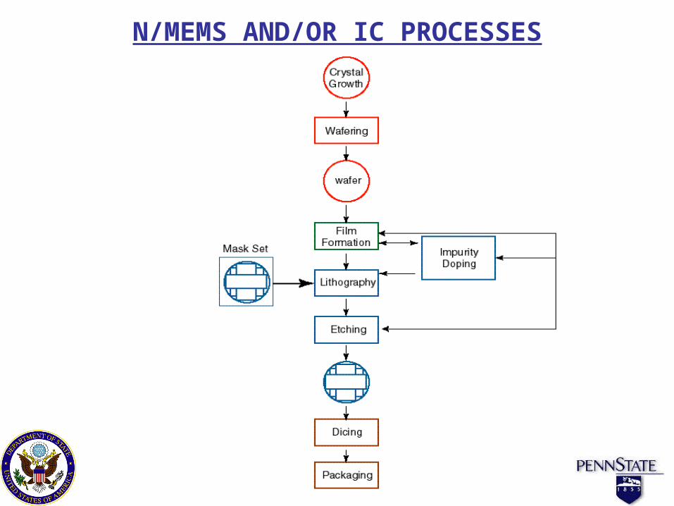
N/MEMS AND/OR IC PROCESSES

Engineering Materials :1) Metals.2) Semiconductors.3) Ceramics.4) Polymers.
Electronic Materials :- Comprise materials from all of the four engineering materials categories.- They have no common physical or chemical properties : their electrical properties span the range from nearly-ideal insulators to excellent conductors.- They are important in IC and N/MEMS fabrication.
MATERIAL FOR N/MEMS AND/OR ICs

• To fabricate ICs and N/MEMS many different kinds of bulk materials and thin films are used.• The bulk materials are predominantly semiconductors.• The most important semiconductor for ICs and N/MEMS is Si.• Thin films in ICs and N/MEMS are classified into four groups:
ELECTRONIC MATERIALS
Thin films
thermal SiO2 dielectrics Poly-Si metals
Deposited SiO2 Deposited Si3N4

Metallization
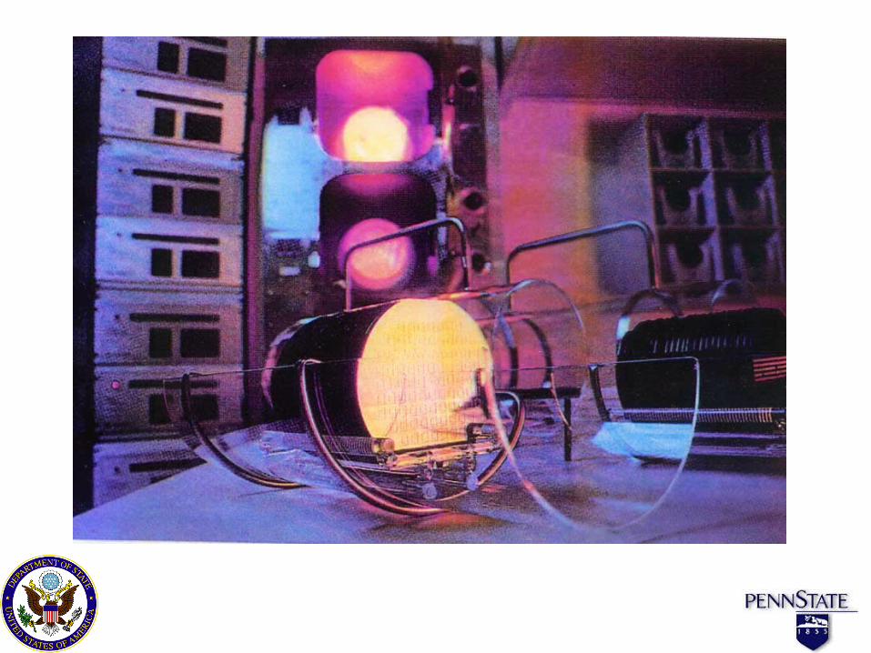
- Metallization is a process whereby metal films are formed on the surface of a substrate.
- The most common and important metallization method is physical vapor deposition (PVD).
- The main PVD processes are evaporation and sputtering.

Highlights of a Typical Evaporation Process

- Open evaporator.

- Remove wafer holder.

- This is where the wafers will be during the evaporation process.
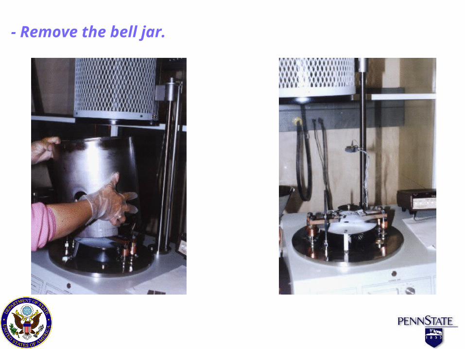
- Remove the bell jar.
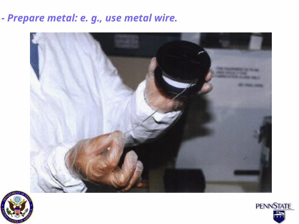
- Prepare metal: e. g., use metal wire.
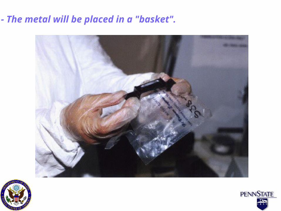
- The metal will be placed in a "basket".

- Some evaporators use a "coil" instead of a "basket".
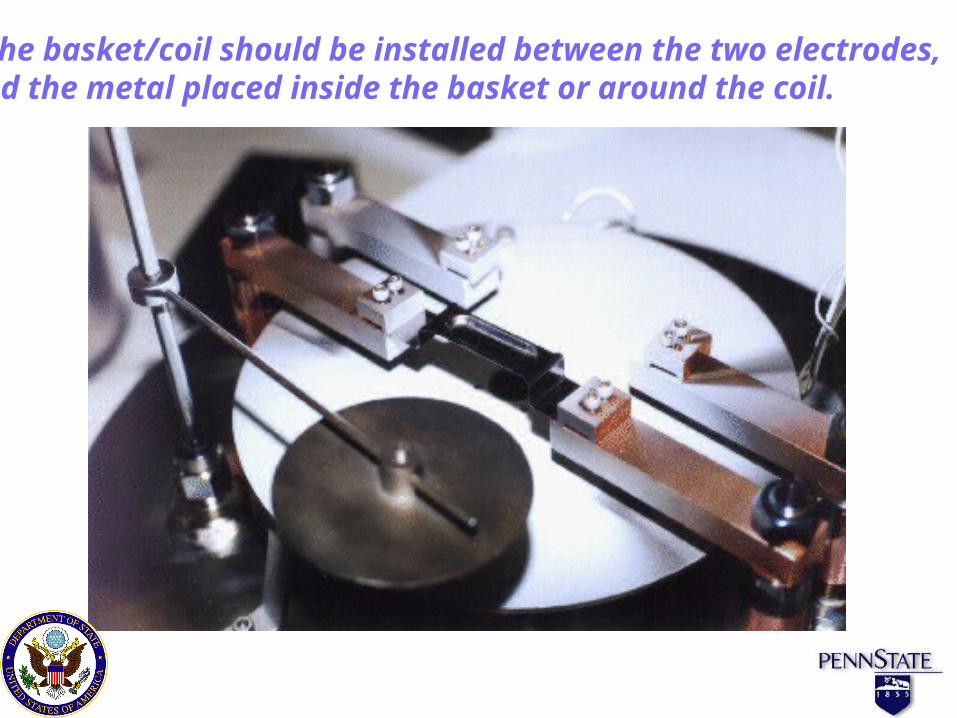
- The basket/coil should be installed between the two electrodes,and the metal placed inside the basket or around the coil.

- Move shutter to cover the filament.
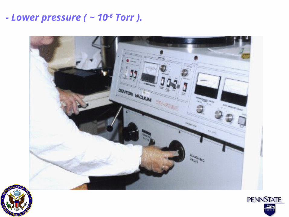
- Lower pressure ( ~ 10-6 Torr ).

- Heat the filament to evaporate the metal.
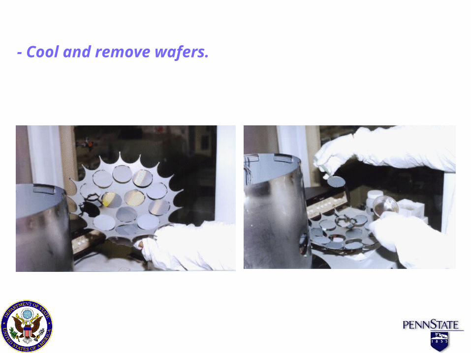
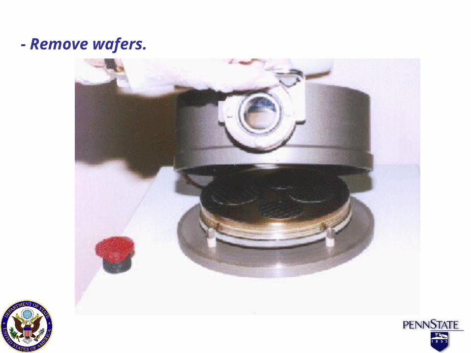
- Cool and remove wafers.

- The test wafer allows measurement of film thickness.
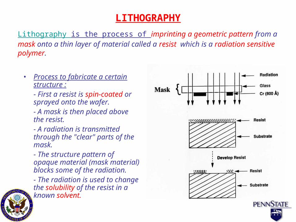
Lithography is the process of imprinting a geometric pattern from a mask onto a thin layer of material called a resist which is a radiation sensitive polymer.
• Process to fabricate a certain structure :- First a resist is spin-coated or sprayed onto the wafer.- A mask is then placed above the resist.- A radiation is transmitted through the "clear" parts of the mask.- The structure pattern of opaque material (mask material) blocks some of the radiation.- The radiation is used to change the solubility of the resist in a known solvent.
LITHOGRAPHY
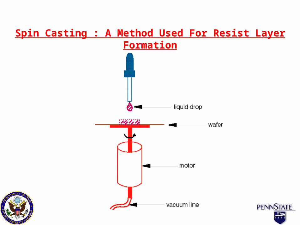
Spin Casting : A Method Used For Resist Layer Formation
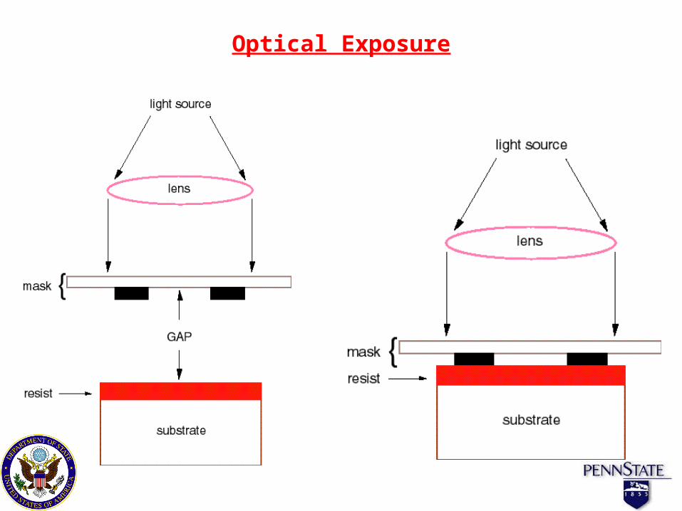
Optical Exposure

Highlights of a Typical Lithography Process
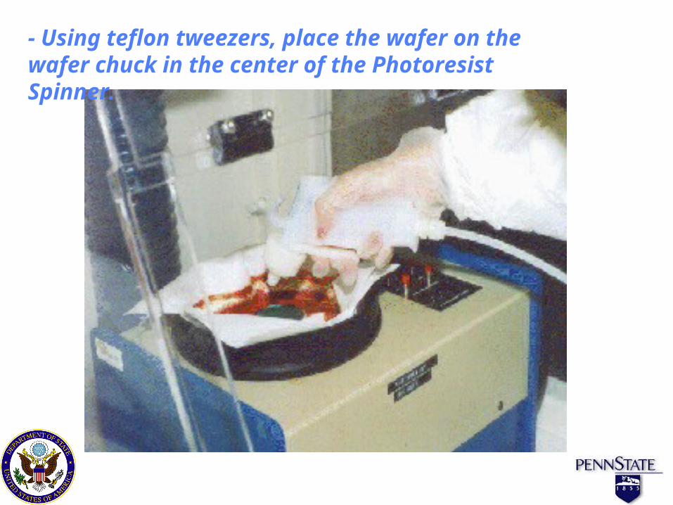
- Using teflon tweezers, place the wafer on the wafer chuck in the center of the Photoresist Spinner.

- Press the spin button which will cause the wafer to spin at ~ 5000 rpm. Centrifugal force will cause excess primer to move away from the center until all wafer is primed and ready to accept resist. Then release spin button.

- Give the resist a soft-bake in an oven at temperatures between 90 and 120 °C to semi-harden the resist. Meanwhile setup the mask aligner.

- For each layer there is a separate mask (patterned glass).

- Place the mask in the wafer holder so that the emulsion side of the mask is facing downward toward the wafer.
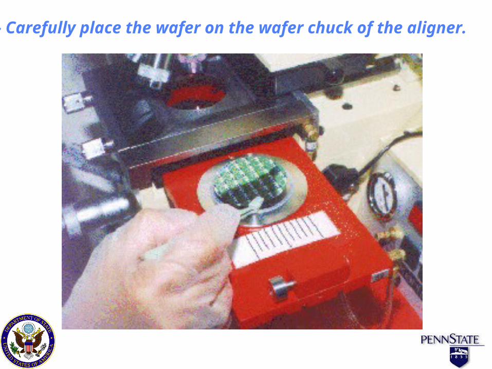
- Carefully place the wafer on the wafer chuck of the aligner.
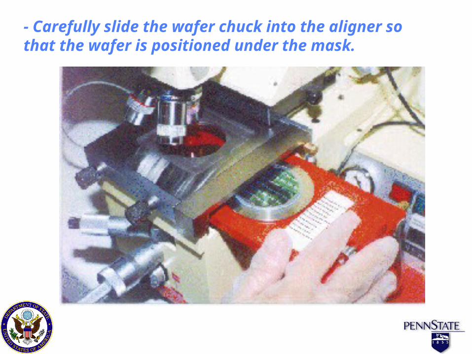
- Carefully slide the wafer chuck into the aligner so that the wafer is positioned under the mask.
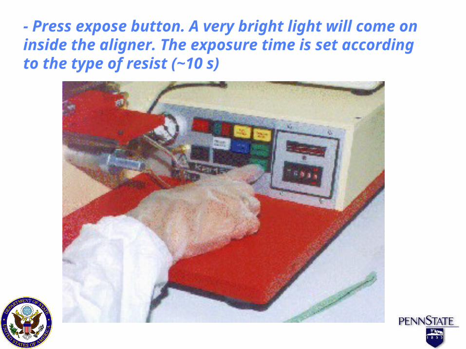
- Press expose button. A very bright light will come on inside the aligner. The exposure time is set according to the type of resist (~10 s)
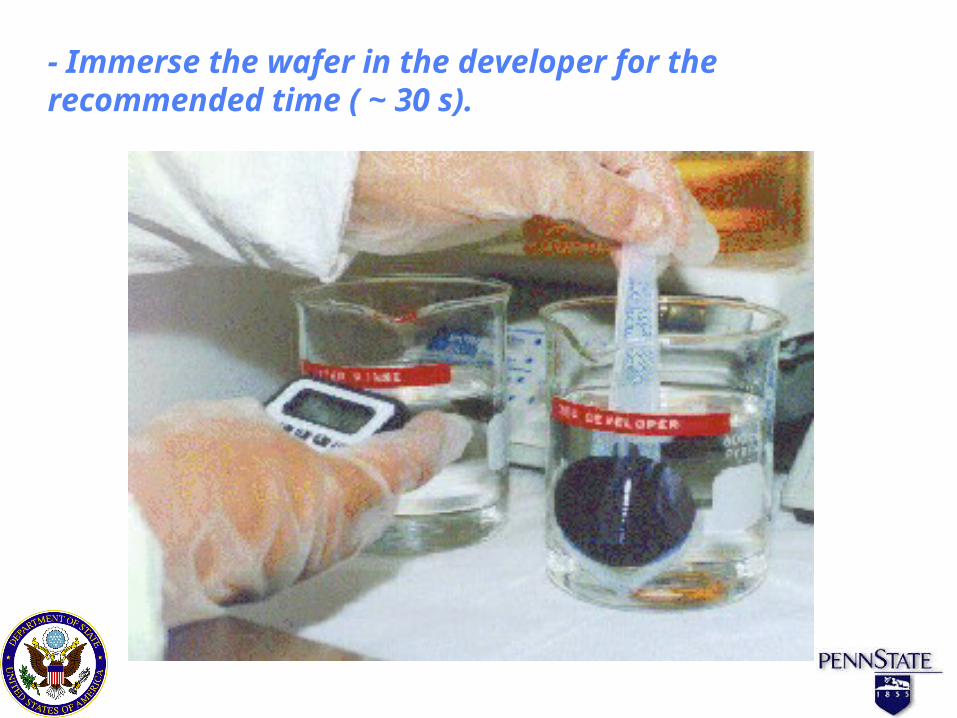
- Immerse the wafer in the developer for the recommended time ( ~ 30 s).

- Immediately after plunge the wafer into the beaker filled with water to stop the development process.
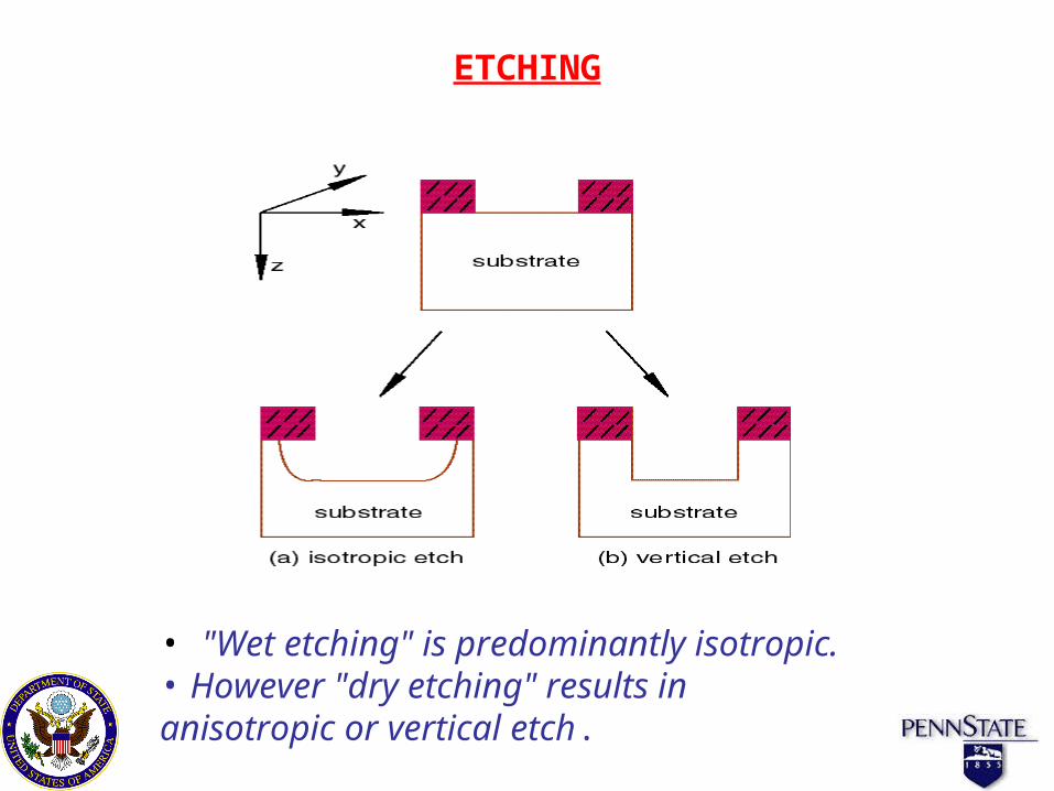
ETCHING
• "Wet etching" is predominantly isotropic.• However "dry etching" results in anisotropic or vertical etch.

Dry Etching
(1) Vacuum enclosure ; (2) At least two electrically separated electrodes ; (3) Provision for continuous introduction of etching gas ; (4) A port for pumping ; (5) A source of rf coupled to the electrodes to create plasma.

Highlights of a Typical Dry Etching Process

- Prepare chamber.

- Load wafers.

-Plasma etch.
- Remove wafers.
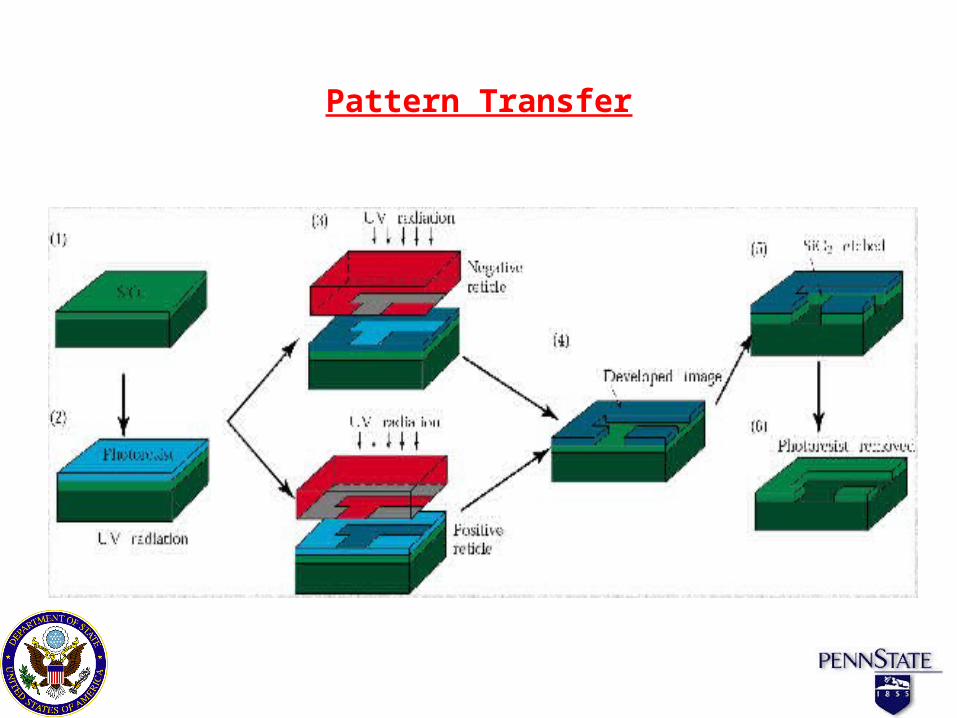
Pattern Transfer
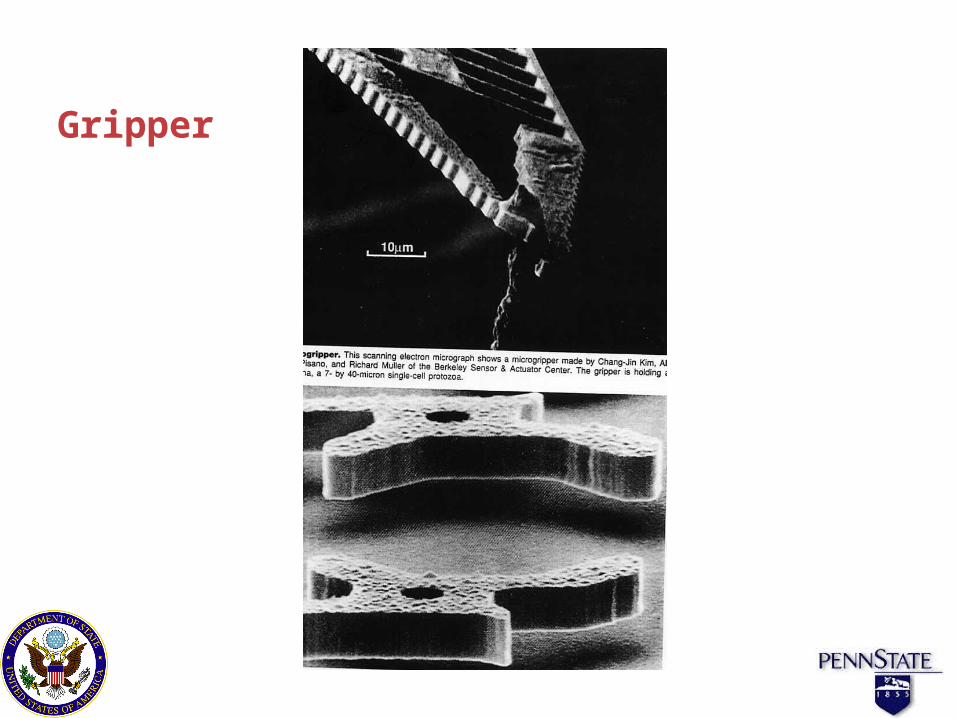
Gripper
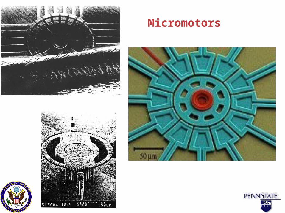
Micromotors


![Reliable Research: Towards Experimental Standards for Computer Science [by Justin Zobil] Presented by: Osama Alsaadoun.](https://static.fdocuments.us/doc/165x107/56649d825503460f94a678ab/reliable-research-towards-experimental-standards-for-computer-science-by.jpg)