
Nanochip VOL11 ISS1r1 - Applied Materials
23
8 20 28 Automotive electronics: Gearing up Piezo Effect Boosts MEMS Microphones, Fingerprint Sensors Automotive Power Device Market Amps Up Driving Innovation: Cars And Electronics Converge V11/Issue 1/2016 Solutions for Factory and Equipment Efficiency
Transcript of Nanochip VOL11 ISS1r1 - Applied Materials

8 20 28
Automotive electronics: Gearing up
Piezo E� ect Boosts MEMS Microphones, Fingerprint Sensors
Automotive Power Device Market Amps Up
Driving Innovation:Cars And Electronics Converge
V11/Issue 1/2016
Solutions for Factory and Equipment Efficiency

NANOCHIP 1
Get More from 200mm Producers with Vita Controllers
12
Technology trends sometimes have a way of sneaking up on us. For the past few years, chip manufacturers have focused on supplying ICs for the latest smartphones, tablets, PCs, and other consumer electronics. Now, even as that market seems to have leveled o� , the automotive segment continues to grow, fueled by a myriad of convenience and safety innovations as well as the pursuit of self-driving cars. As a result, automotive semiconductor revenue is growing at nearly twice the rate of the overall semiconductor market.
That’s why automobiles take center stage in this issue of Nanochip Fab Solutions. Our cover story, “Driving Innovation,” discusses the automotive industry in this milestone period, heralding decades of change—change that will directly impact semiconductor manufacturing.
In a recent presentation at imec ITF 2016, in Brussels, Belgium, Audi executive Berthold Hellenthal noted that today 80% of all automotive innovations depend on semiconductors. Everything from sensors and 3D video cameras to night vision and long-range radar relies on ICs. And this dependency touches every aspect of the automotive business, including quality, costs, and supplies.
German consultants PwC (whose fi gures Hellenthal cited at imec), estimate that electronic components, which currently represent less than 30% of a vehicle’s manufacturing cost, will represent 50% by 2030. Nanochip Fab Solutions examines both technology and market drivers behind this projected growth. Our readers will soon learn why the need to supply ICs for electric vehicles (EVs), self-driving vehicles, and advanced driver assistance system (ADAS) features is tightening the relationship between automakers and chip manufacturers more than ever.
We also look at the interesting phenomenon of manufacturing new, highly sophisticated ICs, such as advanced power devices and MEMS for auto sensors, using more cost-e� ective legacy tools. One article, for example, explores how the MEMS industry is getting a boost from companies interested in using the piezoelectric e� ect and new materials like scandium to build next-generation microphones and fi ngerprint sensors—two high-volume products that could have a major impact on 200mm semiconductor manufacturing. While challenges remain, Applied is now working with leading technologists to develop a new class of MEMS devices that leverage this important technology.
Our article on FabVantage 360 introduces a new benchmarking service that gives customers a “big picture” view of their fab operations, enabling them to see how their tool performance compares to the world’s best-in-class facilities. This capability touches on an issue that is particularly important to automotive device manufacturers: the ability to ensure the safety of devices they produce for automotive applications through critical analysis of process control (FDC) and detection of deviations early in the production process rather than later at fi nal test.
Finally, two related articles introduce Applied Materials’ redesigned 200mm Centura Epi chamber and Vita controller for 200mm Applied Producer tools. The new Epi chamber delivers the superior quality thick epi required for MEMS and other power device applications without compromising results for thinner layers. The Vita controller, previously available for 200mm Centura and Endura systems, has now been extended to 200mm Producer tools, enabling high resolution and data clarity, with total recipe transparency and backward-compatibility with the original software.
Cars and chips. Less than a decade ago this would not have been the most obvious of pairings, but this will be a key driver of our industry today. And as you’ll read in the following pages, we’d better fasten our seatbelts and gear up: it’s going to be an exciting ride!
ALI SALEHPOURSENIOR VICE PRESIDENT
AND GENERAL MANAGER, NEW MARKETS AND
SERVICE GROUP
CONTENTS
25Automotive ICs Lead Market Growth
20Driving Innovation: Cars and Electronics Converge
PLUS:
31: Inline SEM Electron Beam Review Accelerates LTPS Display Yield Ramps
36: Aeris-S Technology: Increase Subfab Safety, Reduce Emissions
40: New Preventive Maintenance Service Option
41: The Last Word: Never Say Never to Moore’s Law
HOW AUTOMOTIVE INNOVATION IS DRIVING SEMICONDUCTOR MANUFACTURINGA Letter from Ali Salehpour2
Piezo E� ect Boosts MEMS Microphones, Fingerprint Sensors
Stepping Back from the Canvas
New High-Productivity Epi Chamber for
Thick Silicon Epitaxy
8
CARS AND CHIPS:
17
28 Automotive Power Device Market Amps Up
P U B L I S H E RPeggy Marcucci
E D I T O R - I N - C H I E FLiz Baird
T E C H N O L O G Y A D V I S O RHelen Armer
C O N T R I B U T I N G E D I T O R SGary Dagastine
Jeannette Ho� manDavid Lammers
Jill O’Nan
D E S I G NJane Olson Graphic Design
NANOCHIP is published by Applied Materials, Inc.
© Copyright Applied Materials, Inc., 2016
www.appliedmaterials.com
Nanochip Fab Solutions is now delivered in an environmentally friendly online version.
Printed copies are available upon request. For a free subscription, or to
add colleagues to the mailing list,please send an email to
[email protected] with the following information:
• Name • Title • Company • Business address • Business email*
*Sorry—no general accounts, e.g., Gmail, AOL, Yahoo
All trademarks so designated or otherwise indicated as product names
or services are trademarks of Applied Materials, Inc. in the U.S. and other countries. All other product and
service marks contained herein are trademarks of their respective owners.
8
Epi Chamber for Thick Silicon Epitaxy
Epi Chamber for Thick Silicon Epitaxy
Get More from 200mm Producers with Vita Controllers
20Driving Innovation:
17

NANOCHIPNANOCHIP2 3
NEW HIGH-PRODUCTIVITY
EPI CHAMBER FOR THICK SILICON EPITAXY
BY CARLOS CABALLERO
Semiconductor technology is undergoing a sea change as proliferating mobile technologies and the growing Internet of Things broaden the use of semiconductors in more products across more market segments than ever before. Among many design and manufacturing changes, these forces are stimulating the fabrication of devices in which performance is enhanced by using much thicker fi lms than are typically associated with semiconductors. Applications calling for thick epitaxial silicon (Si) can now benefi t from a versatile new single-wafer chamber specifi cally designed for that purpose. A new Centura Epi chamber has a >6µm/min. growth rate that enables more than 100µm of silicon epitaxy in a single pass through exceptional chemical e� ciency, delivering both high productivity and lower cost of ownership.
Today’s semiconductor industry may be more dynamic than ever before. While leading-edge chip designers explore the far frontier of scaling below 10nm, a growing variety of devices are being fabricated using fi lms that are thousands of times thicker. Thick, doped epitaxial Si forms electrical isolation for higher-voltage, faster-switching power semiconductors, such as insulated-gate bipolar transistors (IGBTs), used in appliances, stereos, trains, etc. It also improves device performance and lowers manufacturing costs of price-sensitive sensors and actuators by incorporating microelectromechanical systems (MEMS) in power-e� cient, “smart” applications.
Commercially viable manufacturing of power devices and advanced MEMS requires epitaxial Si 30–150µm thick to be grown on systems that deliver high productivity at the lowest possible cost of ownership. Many of these devices can be cost-e� ectively manufactured on 200mm systems and are rejuvenating the market for this equipment. Applied Materials actively supports the expansion of 200mm technologies and has enhanced the capabilities of several of its 150mm and 200mm systems—including its widely used 200mm Applied Centura Epi chamber—to meet evolving industry requirements.
A pioneer in epitaxy and the market leader in epitaxial deposition equipment, Applied Materials has leveraged its long-established expertise in materials engineering to redesign the 200mm Centura Epi chamber specifi cally for superior quality thick Si (20–100µm) without compromising its already excellent results for thinner layers (<20µm). The new 200mm Applied Centura Epi chamber features process kit modifi cations that combine to enable (1) growth of up to 100µm of Si in a single pass; (2) shorter clean time compared to that of a standard chamber; (3) multi-wafer processing between cleans (for <20um); and (4) signifi cantly lower consumable costs.

NANOCHIPNANOCHIP4 5
Once an epitaxy tool is fully depreciated, running cost has a major direct impact on profi tability, so tight control of consumable costs is critical to overall profi tability.
UPGRADING THE CHAMBER
Power devices and MEMS require extremely uniform epitaxial Si and resistivity of less than 2%. To meet these demands, key hardware and software components of the standard 150mm and 200mm Centura Epi chambers were upgraded for the new Epi chambers.
Figure 1. New motorized lift minimizes wafer motion within the susceptor slot.
Y-ax
is (m
m)
1.2
1.0
0.8
0.6
0.4
0.2
0
-0.2
-0.4
-0.6
-0.8
-1.0
-1.2
X-axis (mm)-1.2 -1.0 -0.8 -0.6 -0.4 -0.2 0 0.2 0.4 0.6 0.8 1.0 1.2
Wafer Position After4 sec
10 sec20 sec
Figure 2. Exact wafer positioning achieved with the motorized lift produces less than 1% variation in fi lm thickness between wafers.
Nor
mal
ized
Thi
ckne
ss (A
.U.)
1,030
1,020
1,010
1,000
990
980
970-100 0 100
Wafer Diameter (mm)
Slot 5
Slot 10
Slot 15
Slot 20
Slot 25
Chamber: Process kit geometries were modifi ed to achieve a smaller boundary layer, i.e., zone of highest precursor concentration above the wafer surface. This promotes faster fi lm growth by more e� ectively containing the trichlorosilane (TCS) Si precursor in the reaction space above the wafer surface. The resulting boost in chemical e� ciency reduces the volume and cost of TCS required by the process.
Several design changes to other components improve laminar gas fl ow to facilitate higher growth rates, improve uniformity of fi lm growth and resistivity, and reduce unintentional coating of chamber components, including the upper and lower dome. Reduced coating is particularly important in ensuring good temperature uniformity and stable fi lm growth across the entire wafer.
Motorized Susceptor Lift: The Applied Centura Epi system can accommodate up to three of the newly-designed chambers. In each chamber, a wafer rests in a pocket on a susceptor that rotates while precursor gas is injected into the chamber and the epitaxial process takes place. Exact positioning of the wafer is essential for optimizing within-wafer uniformity of the epitaxial layer and wafer-to-wafer repeatability of the process. Therefore, in the new chambers, the conventional pneumatic susceptor lift has been replaced with a motorized lift whose speed can be much more carefully controlled to avoid wafer movement within the susceptor pocket (see fi gure 1). A new susceptor-leveling mechanism complements the motorized lift to enhance positioning repeatability (see fi gure 2).
Reliable centering of wafers also minimizes bridging, i.e., the tendency of wafers to stick to the susceptor. This e� ect can occur when the susceptor surface is exposed between the edge of the wafer and the pocket sidewall, allowing epitaxial growth to spread over this area.
Closed-loop dome temperature control: This new software feature has the dual benefi t of improving on-wafer performance and boosting system productivity. Maintaining a stable process environment temperature (see fi gure 3) is important for promoting the desired single-crystal growth. Closed-loop temperature control also helps minimize coating of the dome.
Minimal coating has implications for both fi lm quality and system productivity. Producing thicker fi lms requires longer process times, increasing the possibility that coatings or byproducts will build up on chamber surfaces.
Figure 3. Closed-loop temperature control eliminates undesirable variance in dome temperature.
Tem
p C
Time
Dome Temperature Stability WITHOUT CLC
Deposition Step
Tem
p C
Time
Dome Temperature Stability WITH CLC
Deposition Step
Chamber Current Step 1
Quartz (Aux) Pyrometer Temp 1
Chamber Current Step 1
Quartz (Aux) Pyrometer Temp 1
The thicker the deposits, the greater the risk that the material will fl ake o� and fall onto the wafer, creating yield-limiting defects.
From a productivity standpoint, a thin coating can be removed speedily and with only a small volume of hydrochloric acid (HCL). This contributes to lowering the cost of consumables, and lessens the system’s potential environmental hazards. For thinner epitaxy (≤20µm), negligible dome coating allows throughput of three wafers between chamber cleans rather than only one, as is typically the case.
IMPROVING PERFORMANCE
As summarized in table 1, the modifi cations described earlier enable Applied’s new epi chamber to satisfy all key market requirements by mitigating the major challenges posed by thick epitaxy. It achieves an unmatched growth rate of high-quality Si, formed with excellent thickness and doping uniformity and negligible defectivity. In addition, it ensures repeatable wafer placement and eliminates bridging, which are both essential for high-yield volume manufacturing. Moreover, this industry-leading performance is delivered at a lower cost of operation than competing alternatives o� er.
Table 1. Applied’s new Centura Epi chamber satisfi es all market requirements for thick epitaxy. (Data shown is for a 3-chamber system.)
100nµm EPITAXY ATTRIBUTE MARKET REQUIREMENT PERFORMANCE
Growth Rate ~6µm/min
WiW Thickness Nonuniformity <1.5% <1.5% FTIR
WtW Thickness Nonuniformity <1.5% <1.5% FTIR
WiW Rs Nonuniformity <2% <2% (30Ω/cm) (HgCv, 4pt probe)
WtW Rs Nonuniformity <2% <2% (30Ω/cm) (HgCv, 4pt probe)
Metallic Contamination <5e10 <5e10 (TXRF)
Particles (Total Adders @>0.16µm) <10 <10 (SP1/Surfscan)
Slip None None
Transition Width <10µm <10µm
Throughput 6 6
NEW HIGH-PRODUCTIVITY
EPI CHAMBER FOR THICK SILICON EPITAXY

NANOCHIPNANOCHIP6 7
Figure 4 illustrates the higher growth rate produced by the new, smaller Centura Epi chamber and more e� cient chemistry, while fi gure 5 shows the uniformity of thickness and resistivity achieved. The new chamber o� ers the versatility of equally good results for both thick and thin epitaxy (see fi gure 6). Resistivity targets are reached rapidly and remain stable throughout the entire growth process (see fi gures 7–8).
SUMMARY
With the introduction of the new Centura Epi chamber, Applied Materials has signifi cantly upgraded its workhorse 150mm and 200mm
Figure 4. With a 20% higher growth rate than standard epitaxy for the same precursor fl ow, the new Centura Epi system improves throughput by up to 25% over its predecessor.
Gro
wth
Rat
e (µ
m/m
in)
8
7
6
5
4
3
2
1
00 15105 20 25 30
TCS Flow (slm)
STD Chamber GR (µm/min)
HGR GR (µm/min)
Figure 5. Results from a 500-wafer marathon demonstrate tight thickness and resistivity control for 100µm epitaxial Si produced in the Applied Centura Epi chamber.
Figure 6. Equally good performance for thick and thin fi lms substantiate the versatility of the Applied Centura Epi chamber.
Resi
stiv
ity (o
hms/
cm)
41.3
40.1
38.9
37.7
36.5-100 0-25-75 25 75-50 50 100
Distance From Center (mm)
Thic
knes
s (µm
)
107.5
105.0
102.5
100.0
97.5-100 0-25-75 25 75-50 50 100
Distance From Center (mm)
Y axis
X axis
Y axis
X axis
Thickness Resistivity
Resi
stiv
ity (o
hms/
cm)
Uni
form
ity (+
/- %
)
Uni
form
ity (+
/- %
)
Thic
knes
s (µm
)
120
100
80
60
40
20
0
3.0%
2.5%
2.0%
1.5%
1.0%
0.50%0 600400200 800 1000 1200
Process Time (sec)
40
35
30
25
20
15
10
5
0
3.0%
2.5%
2.0%
1.5%
1.0%0 600400200 800 1000 1200
Process Time (sec)
Rs (ohms/cm)
Uniformity (+/- %)
Thickness (µm)
Uniformity (+/- %)
Average Growth Rate 6.01µm/min
Figure 7. Marathon results illustrate consistently tight transition width and stable resistivity through the 100µm-thick Si layer for the Applied Centura Epi chamber.
Resi
stiv
ity (o
hms/
cm)
1.0E+02
1.0E+01
1.0E+00
1.0E-01
1.0E-02
1.0E-03
Resi
stiv
ity (o
hms/
cm)
1.0E+02
1.0E+01
1.0E+00
1.0E-01
1.0E-02
1.0E-03100 90 80 70 60 50 40 30 20 10 0 -10 100 90 80 70 60 50 40 30 20 10 0 -10
Depth (µm) Depth (µm)
CTR
EE5mm
CTR
EE5mm
Wafer 1 Wafer 500
Figure 8. The spreading resistance profi le for a two-fi lm layer in an IGBT shows narrow transition widths for both low and high resistivity target values and stability throughout each of the layers produced in the Applied Centura Epi chamber.
Resi
stiv
ity (o
hms/
cm)
1.0E+03
1.0E+02
1.0E+01
1.0E+00
1.0E-0170 6065 55 50 45 40 35 30 25 20 15 10 5 0 -5
Depth (µm)
CTR
EE5mm
Centura Epi chambers to meet the industry need for cost-e� ective production of thick Si in power-device and MEMS applications. In a 500-wafer marathon, the redesigned chamber demonstrated a >6µm/min growth rate in producing 100µm-thick blanket silicon—triple that of batch technology. In addition, its chamber design and shorter process times promote optimum e� ciency and productivity of the TCS precursor, a cleaner chamber, and lower consumption of HCL used in removing dome coating. These economies o� er the competitive benefi ts of a lower cost of consumables relative to batch systems, as well as higher throughput.
For additional information, contact [email protected]
NEW HIGH-PRODUCTIVITY
EPI CHAMBER FOR THICK SILICON EPITAXY

NANOCHIPNANOCHIP8 9
PIEZO EFFECT BOOSTS MEMS MICROPHONES, FINGERPRINT SENSORS
The MEMS industry is getting a push from companies interested in taking advantage of the piezoelectric e� ect to build next-generation microphones and fi ngerprint sensors—two high-volume products that could have a major impact on the 200mm semiconductor landscape.
MEMS Microphone Technology Roadmap
Traditional capacitive MEMS microphones
Sign
al-t
o-N
oise
Rat
io (d
B)
85
80
75
70
65
60
2010 2011 2012 2013 2014 2015 2016 2017 2018 2019
Piezoelectric (Vesper)
Next-generation capacitiveMEMS microphone
Optical MEMS microphones,e.g., Silicon Audio
Figure 1. Microphone architectures that leverage new materials and new sound-wave detection schemes promise increased signal-to-noise performance. (Source: IHS)
New materials and architectures for MEMS microphones and fi ngerprint sensors—both major revenue streams for the MEMS industry—use the piezoelectric e� ect: the ability of certain materials to generate an electric charge in response to applied mechanical stress (see sidebar, “The Piezoelectric E� ect”).
Though challenges remain, technologists are working with Applied Materials to develop a new class of MEMS devices that leverage this important technology.
HIGH SNR MICROPHONES
MEMS-based microphones—one of the highest-volume MEMS devices produced today—are undergoing a seismic shift in capabilities (see fi gure 1). A move is underway from single parallel-plate, capacitive-coupled microphones to piezo-based microphones, soon to be followed by electrostatic comb-fi nger-based designs and then optical-based devices. While it is the piezo-based design that has captured attention recently, experts agree it will take time to develop the necessary materials and process technologies required to mass produce the devices with high reliability.
A recent forecast by Yole Développement (Lyon, France) puts shipments of MEMS microphones in 2016 at over 4.4B units, exceeding 7B units by 2020, a nearly 14% compound annual growth rate (CAGR) over the forecast period.
Microphones used inside the cabins of cars and trucks are expected to be a key driver, provided that the signal-to-noise ratio (SNR) can be improved enough
to fi lter out street noises. Most cars and trucks still use older electret-style devices. However, a change is underway as the SNR of MEMS-based microphones improves, the number of microphones per vehicle increases, and more emphasis is placed on triangular noise cancellation and directionality.
IMPROVED SNR OPENS DOORS
Matt Crowley, CEO of Boston-based Vesper, a piezo-MEMS microphone startup, expects that the increased SNR capability (beyond 70dB) of next-generation microphones “will open up numerous additional applications in consumer and industrial markets,” ushering in an era of voice-activated, recognition-based technologies.
PVD-sputtered piezo materials, including scandium-doped aluminum nitride (ScAlN),[1] are enabling much of
this improved performance. Theoretical calculations demonstrate that the higher the scandium concentration, the more improved the SNR will be.
Crowley calculates that for every 5% of scandium (Sc) there is a corresponding increase of 1dB of SNR, which is signifi cant from both application performance and manufacturing standpoints.
Today there are readily available single-alloyed targets containing less than 10% Sc. However, for higher concentrations the target alternatives are not well developed. Applied Materials, in conjunction with target manufacturers, is tackling the development of higher-concentration Sc-doped single-alloy targets, as well as the robust deposition processes needed to deliver them in a manufacturing environment. The goal is to enable deposition processes to support Sc concentrations up to 43%—the empirically proven limit before there is a roll o� in the achieved piezoelectric coe� cient.
BY MIKE ROSA, PhD
Piezo microphone images courtesy of Vesper Technologies, Inc.
Proprietary Piezoelectric Transducer
Submicron CMOS ASIC
NANOCHIPNANOCHIP10 11NANOCHIP 11
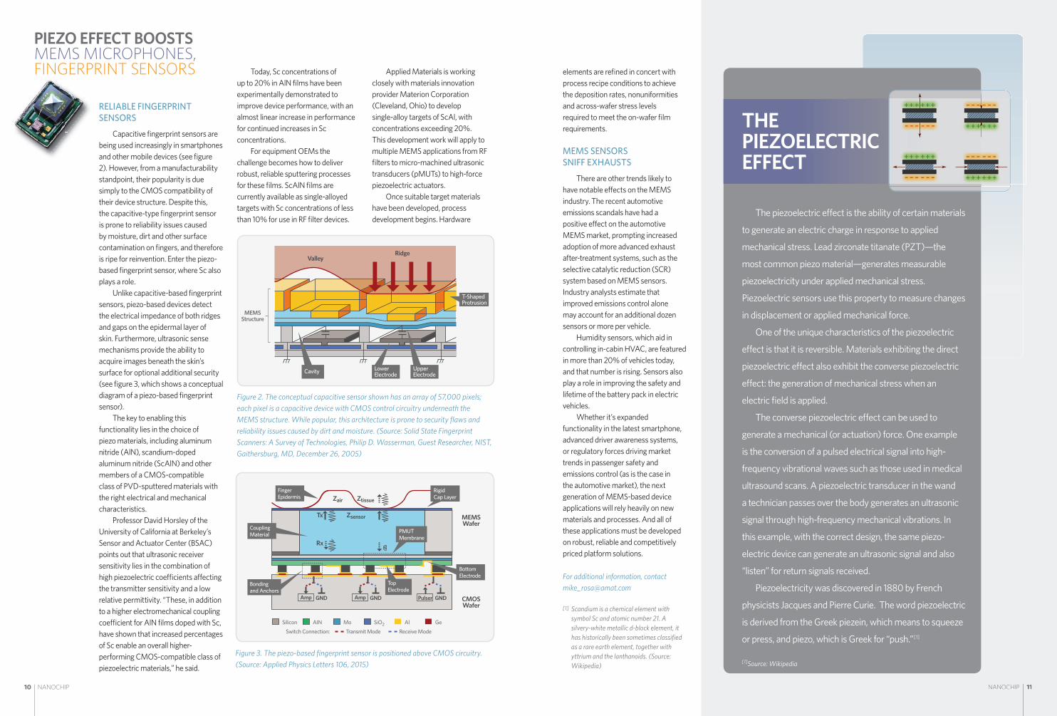
RELIABLE FINGERPRINT SENSORS
Capacitive fi ngerprint sensors are being used increasingly in smartphones and other mobile devices (see fi gure 2). However, from a manufacturability standpoint, their popularity is due simply to the CMOS compatibility of their device structure. Despite this, the capacitive-type fi ngerprint sensor is prone to reliability issues caused by moisture, dirt and other surface contamination on fi ngers, and therefore is ripe for reinvention. Enter the piezo-based fi ngerprint sensor, where Sc also plays a role.
Unlike capacitive-based fi ngerprint sensors, piezo-based devices detect the electrical impedance of both ridges and gaps on the epidermal layer of skin. Furthermore, ultrasonic sense mechanisms provide the ability to acquire images beneath the skin’s surface for optional additional security (see fi gure 3, which shows a conceptual diagram of a piezo-based fi ngerprint sensor).
The key to enabling this functionality lies in the choice of piezo materials, including aluminum nitride (AlN), scandium-doped aluminum nitride (ScAlN) and other members of a CMOS-compatible class of PVD-sputtered materials with the right electrical and mechanical characteristics.
Professor David Horsley of the University of California at Berkeley’s Sensor and Actuator Center (BSAC) points out that ultrasonic receiver sensitivity lies in the combination of high piezoelectric coe� cients a� ecting the transmitter sensitivity and a low relative permittivity. “These, in addition to a higher electromechanical coupling coe� cient for AlN fi lms doped with Sc, have shown that increased percentages of Sc enable an overall higher-performing CMOS-compatible class of piezoelectric materials,” he said.
Today, Sc concentrations of up to 20% in AlN fi lms have been experimentally demonstrated to improve device performance, with an almost linear increase in performance for continued increases in Sc concentrations.
For equipment OEMs the challenge becomes how to deliver robust, reliable sputtering processes for these fi lms. ScAlN fi lms are currently available as single-alloyed targets with Sc concentrations of less than 10% for use in RF fi lter devices.
Applied Materials is working closely with materials innovation provider Materion Corporation (Cleveland, Ohio) to develop single-alloy targets of ScAl, with concentrations exceeding 20%. This development work will apply to multiple MEMS applications from RF fi lters to micro-machined ultrasonic transducers (pMUTs) to high-force piezoelectric actuators.
Once suitable target materials have been developed, process development begins. Hardware
PIEZO EFFECT BOOSTS MEMS MICROPHONES, FINGERPRINT SENSORS
ValleyRidge
MEMSStructure
UpperElectrode
LowerElectrodeCavity
T-ShapedProtrusion
Figure 2. The conceptual capacitive sensor shown has an array of 57,000 pixels; each pixel is a capacitive device with CMOS control circuitry underneath the MEMS structure. While popular, this architecture is prone to security fl aws and reliability issues caused by dirt and moisture. (Source: Solid State Fingerprint Scanners: A Survey of Technologies, Philip D. Wasserman, Guest Researcher, NIST, Gaithersburg, MD, December 26, 2005)
GNDPulserGNDAmpGNDAmp
Zair Ztissue
ZsensorTx
Rx
MEMSWafer
CMOSWafer
FingerEpidermis
RigidCap Layer
CouplingMaterial
Bondingand Anchors
PMUTMembrane
BottomElectrode
TopElectrode
Silicon AIN Mo SiO2 Al GeTransmit ModeSwitch Connection: Receive Mode
Figure 3. The piezo-based fi ngerprint sensor is positioned above CMOS circuitry. (Source: Applied Physics Letters 106, 2015)
elements are refi ned in concert with process recipe conditions to achieve the deposition rates, nonuniformities and across-wafer stress levels required to meet the on-wafer fi lm requirements.
MEMS SENSORS SNIFF EXHAUSTS
There are other trends likely to have notable e� ects on the MEMS industry. The recent automotive emissions scandals have had a positive e� ect on the automotive MEMS market, prompting increased adoption of more advanced exhaust after-treatment systems, such as the selective catalytic reduction (SCR) system based on MEMS sensors. Industry analysts estimate that improved emissions control alone may account for an additional dozen sensors or more per vehicle.
Humidity sensors, which aid in controlling in-cabin HVAC, are featured in more than 20% of vehicles today, and that number is rising. Sensors also play a role in improving the safety and lifetime of the battery pack in electric vehicles.
Whether it’s expanded functionality in the latest smartphone, advanced driver awareness systems, or regulatory forces driving market trends in passenger safety and emissions control (as is the case in the automotive market), the next generation of MEMS-based device applications will rely heavily on new materials and processes. And all of these applications must be developed on robust, reliable and competitively priced platform solutions.
For additional information, contact [email protected]
[1] Scandium is a chemical element with symbol Sc and atomic number 21. A silvery-white metallic d-block element, it has historically been sometimes classifi ed as a rare earth element, together with yttrium and the lanthanoids. (Source: Wikipedia)
The piezoelectric e� ect is the ability of certain materials
to generate an electric charge in response to applied
mechanical stress. Lead zirconate titanate (PZT)—the
most common piezo material—generates measurable
piezoelectricity under applied mechanical stress.
Piezoelectric sensors use this property to measure changes
in displacement or applied mechanical force.
One of the unique characteristics of the piezoelectric
e� ect is that it is reversible. Materials exhibiting the direct
piezoelectric e� ect also exhibit the converse piezoelectric
e� ect: the generation of mechanical stress when an
electric fi eld is applied.
The converse piezoelectric e� ect can be used to
generate a mechanical (or actuation) force. One example
is the conversion of a pulsed electrical signal into high-
frequency vibrational waves such as those used in medical
ultrasound scans. A piezoelectric transducer in the wand
a technician passes over the body generates an ultrasonic
signal through high-frequency mechanical vibrations. In
this example, with the correct design, the same piezo-
electric device can generate an ultrasonic signal and also
“listen” for return signals received.
Piezoelectricity was discovered in 1880 by French
physicists Jacques and Pierre Curie. The word piezoelectric
is derived from the Greek piezein, which means to squeeze
or press, and piezo, which is Greek for “push.”[1]
[1]Source: Wikipedia
THE PIEZOELECTRIC EFFECT

NANOCHIPNANOCHIP12 13NANOCHIP12
STEPPING BACK CANVASFROM
THE
BYAVI EDELSTEIN
AND HELEN ARMER
New FabVantage 360 Assessments Help Identify Gaps in Tools and Fabs
When working on a painting, artists regularly step back from the canvas to refocus and evaluate their work. Only by taking a broad view can the artist determine what’s working, what’s not, and what to do about it.[1]
Similarly, fab managers can “step back” from their overall operations to evaluate process and equipment performance. Which tools are underperforming? Are equipment constants set correctly? Could a comparison to best known methods (BKMs) help? How could uptime improve? Is my fab output as high as it could be—and am I maximizing ROI?
This article introduces a new Applied Materials benchmarking o� ering, FabVantage 360, which for one fab uncovered opportunities to increase output by 25% as well as reduce particles and defects.
FABVANTAGE 360 —A BROADER PERSPECTIVE
To help fab executives answer the questions above and gain a better perspective on their operations, the Applied Materials FabVantage Consulting Group has developed a new assessment capability, FabVantage 360. This o� ering provides a di� erentiated benchmarking capability to identify opportunities relative to world-class performance and BKMs for evaluated toolsets.
Unlike conventional FabVantage assessments, which normally focus on a specifi c area of concern (such as tool output), a comprehensive FabVantage 360 evaluation delivers a much broader perspective. By taking a wider view, FabVantage 360 can identify more opportunities for tool and fab improvement and help better estimate the impact of these improvements.
Holistic ApproachA FabVantage 360 assessment compares equipment
performance against similar tools across the installed base
and relative to proprietary BKMs. The analysis provides a holistic view of a tool’s performance and can indicate factors that may be interdependent or hidden when the focus is limited to specifi c performance challenges. It also enables customers to prioritize improvement projects by quantifying the magnitude of each identifi ed opportunity. For example, an analysis may reveal that suboptimal cleaning practices are resulting in throughput loss, higher particles, and lower uptime.
Comprehensive ScorecardTo complete an assessment, the FabVantage
360 team develops a comprehensive scorecard that benchmarks a customer’s fab performance on about two dozen metrics. The scorecard covers metrics in four categories of tool performance—confi guration, maintenance, unit process, and output (see table 1). Together, these categories give a picture of a tool’s impact on fab variability, yield, and output. The metrics are scored on a scale of 0%, representing worst in class (WIC), to 100%, representing best in class (BIC).
Typically, fab executives engage in a FabVantage 360 assessment when they need to identify opportunities to improve performance of equipment that is bottlenecked or critical for yield performance. The FabVantage 360 analysis quantifi es gaps in each tool-performance metric, augmented by deep domain knowledge.
EXAMPLE SCORECARDFigure 1 illustrates sample sections from a FabVantage
360 scorecard for a 300mm HDP UltimaX chamber used for STI gapfi ll in a logic fab. The results shown are repre-sentative and used for illustrative purposes only. Sections highlighted include (A) confi guration, (B) maintenance, (C) unit process, and (D) output.
Table 1. Metrics for tool performance used in FabVantage 360 assessments.
This Metric Section... Scores the Tool On...
Confi guration Implementing equipment upgrades, matching equipment constants and software across the fl eet, and using the latest software revision.
Maintenance The preventive maintenance (PM) checklist, PM green-to-green (GtG) time, 1st time PM success, and the use of BKM parts.
Unit Process Particle performance and implementation of fault detection and classifi cation (FDC).
Output Uptime and other equipment states, uptime variability, throughput, and tool dedication.

NANOCHIPNANOCHIP14 15
STEPPING BACK CANVASFROM
THE
Installed on All Chambers Installed on Some Chambers Not Installed
PM PERFORMANCE CUSTOMER WIC BIC PERCENTILE
Critical Parts 62% 25% 100% 41%
GtG Time (Hours) 75 73 18 0%
1st Time PM Success % 74% 73% 100% 4%
PM Interval (Wafers) 18,000 15,000 30,000 20%
PM PROCEDURE INSPECT CALIBRATE CLEAN REPLACE OVERALL
Chamber: BKM Tasks Followed 25% 90% 75% 30% 55%
Mainframe: BKM Tasks Followed 90% 50% 45% 95% 70%
FDC PRACTICES CUSTOMER WIC BIC PERCENTILE
% of Critical Sensors Monitored 51% 50% 100% 14%
% of Monitored Sensors That Are Critical 78% 50% 100% 56%
Data Sampling Rate Vary by Sensor All sensors collected at 1 Hz
Use of UVAs, EHMs, and/or MVAs UVAs used, but not EHM or MVA
Fleet-based/Chamber-based Control Limits Chamber-based
Strategy for Defining Stats and Setting Limits All limits are 3 sigma; do not vary limits by recipe
Monitoring Windows Monitor both steady-state and transitions
Use of Golden Tools/Golden Reference Traces No golden tool or reference trace
Use of Interruption Based on FDC Alarms 0.2 Engineer is notified
PARTICLES CUSTOMER WIC BIC PERCENTILE
Avg. Infilm Particle Adders @ 160nm Size (#) 24 26 5 10%
B. Maintenance – Sample Evaluation
C. Unit Process – Sample Evaluation
UPTIME PERFORMANCE CUSTOMER WIC BIC PERCENTILE
Uptime % 90.2% 84.4% 93.5% 64%
Scheduled Down % 6.5% 6.6% 2.2% 2%
Unscheduled Down % 3.3% 6.3% 3.2% 96%
Uptime Variability 0.2 0.25 0.04 19%
D. Output – Sample Evaluation
HARDWARE UPGRADES CHAMBERS DEFECTS/ CoO THROUGHPUT SCORE YIELD
1. Short Nozzle Symmetric Gas Ring, Top O2 0 0%
2. Lid Centering 0 0%
3. RPS Bypass 12 100%
4. Minimum Contact LL Fins 0 0%
5. Minimum Contact Bu¢er Blade 0 0%
6. Cover Wafer Station 0 0%
7. UPI+ Nozzles 0 0%
8. GT Ba¤e 8 67%
9. Cool Gas Feed Block 8 67%
Total Chambers 12 26%
A. Configuration – Sample Evaluation
SOFTWARE TOOLS #TOOLS WITH #TOOLS WITH #TOOLS WITH % LATEST VERSION OLDER VERSION 1 OLDER VERSION 2 INSTALLED
Tool to Tool Matching 4 1 2 1 50%
THROUGHPUT & DEDICATION CUSTOMER WIC BIC PERCENTILE
System Throughput (WPH, steady-state) 17 10 22.6 56%
% of Product/Recipes Run on All Tools 75% 70% 100% 17%
Nine upgrades are available for the 12 UltimaX chambers. Only the RPS bypass is installed across all chambers getting the full defects, cost, and throughput benefits. Some chambers have the GT ba�e (#8) and the cool gas feed block (#9) upgrades. Other upgrades are not installed, therefore missing opportunities to reduce defects. Similarly, not all tools have the latest software installed therefore missing on latest features and causing variation across tools.
For maintenance procedures, a FabVantage 360 assessment compares the customer’s checklists to recommended checklists and frequencies. The score shows how many of the inspection, calibrations, cleaning, and replacement tasks are followed, as well as sourcing quality OEM spares for critical parts. Performance metrics are benchmarked to indicate impact on green to green time and PM success rate. In this example, the customer does not follow recommended maintenance activities and frequency and as a result takes 75h for green to green vs. 18h BIC. PM Success rate is also impacted with only 74% success, leading to more lost time and rework, as well as a quality risk.
A FabVantage 360 assessment also evaluates FDC practices by comparing the sensors the customer monitors against the list of sensors critical to the performance of a specific process. The assessment also compares general FDC practices to BKM’s and highlights areas of opportunity. This figure shows that the customer is monitoring only 51% of critical sensors and can improve sampling data rates as well as golden references. Under Particles, it also identifies a high particle count of 24 vs. benchmark of 5, representing an opportunity to reduce particles by 80%.
To evaluate output performance, the FabVantage team assesses scheduled downtime, unscheduled downtime, and throughput against benchmark levels. FabVantage experts also analyze production runs to highlight hidden tool dedications. The analysis uncovers opportunities for process optimization and matching, leading to a more balanced utilization across tools, and therefore better cycle time through the equipment set.
PM CHAMBER
UPTIME
PM MAINFRAME
CRITICAL PARTS
GtG TIME
1ST TIME PM SUCCESSFDC CRITICAL
SENSORS
PARTICLES
EQUIPMENTCONSTANTS
HARDWARE
DEDICATION
THROUGHPUT
UPTIME VARIABILITY
SOFTWAREMATCHING
Figure 1. A FabVantage 360 assessment involves collecting detailed tool data from customers in exchange for providing a comprehensive scorecard that identifi es tool performance gaps relative to BIC. This example illustrates the data used to generate the scorecard, along with a summary spider chart that graphically shows performance gaps.
BEST INCLASS
LEGEND
WORSTIN CLASS

NANOCHIPNANOCHIP16 17NANOCHIP 17
STEPPING BACK CANVASFROM
THE Vita’s high computational bandwidth brings a growing number of advanced capabilities to Applied’s popular and versatile legacy platform.
BY JEFFREY DIETZ AND
FLORENT DUCROT
Many users of Applied Materials 200mm Centura and Endura systems who have comprehensive service agreements are already realizing signifi cant improvements thanks to Applied’s Vita controller, which enables implementation of advanced sensors and other capabilities (see Nanochip Express, April 2016 at www.appliedmaterials.com).
have led to substantial gains in performance, productivity, throughput, tool stability, system availability, and reduction of overall cost of ownership for customers’ manufacturing equipment.
Now, similar benefi ts are available to users of Applied Materials 200mm Producer tools when the system is combined with
KEY TAKEAWAYS
As shown in fi gure 1D, the customer’s uptime is 90.2%, within the benchmark range but scheduled downtime is close to the worst end of the benchmark, o� set by good performance on unscheduled down. The performance metrics give another perspective on the PM performance with long green to green times and a low PM success rate.
Possible issues causing poor PM performance are using non-BKM parts and not following prescribed PM procedures, such as not replacing parts at the recommended frequency and not performing prescribed calibrations. High particles are also a result of poor PM procedures, not leveraging defect-reduction upgrades, and setting equipment constants incorrectly.
Another cause of poor PM performance and high particles relates to matching issues on tools. In this example, software revision does not match across all tools. This, combined with incorrectly set equipment constants, may explain the high tool dedication, which in turn reduces the output of the fl eet.
With a FabVantage 360 assessment, these calculations can be illustrated in a SEMI E10 Equipment States chart that shows the productive time of the tool and a breakdown of nonproductive time. As seen in fi gure 2, low throughput causes total tool productivity of only 63.6%, although the tool is utilized for 80% of the time. This example highlights a hidden opportunity to increase output by 25% by improving maintenance practices and equipment setup. Additional opportunities exist to reduce particles and defects, and improve process control with better FDC practices.
CONCLUSIONIt is said that French artist Henri Matisse was
notorious for spending extended periods of time looking at his paintings, refl ecting on what he had done while plotting his next stroke. He would hold his paintbrush at a distance from the canvas and move it slowly through the air to try out di� erent movements before committing to the next stroke on the canvas.[1]
Similarly, a FabVantage 360 evaluation provides customers with a “big picture” view of their fab situation, enabling them to plot their next “stroke” of improvement gains. The FabVantage 360 evaluation provides valuable data for use in prioritizing projects and quantifying ROI. It o� ers an easy, e� ective way to reveal how a customer’s tool performance and fab operations compare to the world’s best-in-class facilities.
For additional information, contact [email protected]
[1] Fred Mandell and Kathleen Jordon (2010). Becoming a Life Change Artist:
7 Creative Skills to Reinvent Yourself at Any Stage of Life. New York, NY:
Penguin Avery Books. Can also be retrieved at https://books.google.com/
books?isbn=110144231X
Figure 2. Example of a SEMI E10 Equipment States chart from a FabVantage 360 assessment which indicates that this fl eet of four tools su� ers from low productivity.
EngineeringIdle DownUtilized
100
90
80
70
60
50
40
30
63.6
16.4
9.0
6.53.3 1.3
The Vita controller is a powerful embedded system that replaces a number of obsolete, performance-limiting components in the VME architecture, including the single-board controller (SBC). It also upgrades other parts originally shipped with these legacy tools.
Vita controller retrofi ts, which are performed by Applied Materials service personnel,
GET MORE FROM200MM PRODUCERSWITH VITA CONTROLLERS
NANOCHIPNANOCHIP18 19NANOCHIP18 NANOCHIP 19
Applied’s advanced services and data analysis capabilities under a service agreement. The Vita controller provides higher resolution and data clarity, enabling unmatched Producer performance, with total recipe transparency and backward-compatibility with the original software.
With high computational bandwidth and access to tool data at up to 10 Hz with no dropouts (see table 1), Vita enables users to fully implement a wide spectrum of advanced services available under Applied Materials service agreements. These include tool optimization, sophisticated process modeling, and tight integration with Applied’s fabwide automation and equipment engineering system (see fi gure 1).
< 34% PARTICLES REDUCTION
< 40% REDUCTION IN LOT FILM THICKNESS VARIATION
Wafer No.
He
Flow
(scc
m)
Thic
knes
s (Å)
Gas FlowVariation
UnstableParticles
StableGas Flow
ParticlesIn Spec
1200
1100
1000
900
SBC Vita
Table 1. The table compares performance of 200mm Producer tools equipped with the original SBC versus those with the new Vita controller. The higher resolution and faster speed of the Vita system generates much better data, which can be used to increase tool performance.
Figure 1. Compared with the original SBC for 200mm Producer tools, the new Vita controller o� ers greater data resolution, enabling signifi cant reductions in particles and greater uniformity in lot fi lm thickness.
VITA FOR PRODUCER
The Applied Materials 200mm Producer platform was introduced in 1998. Today, more than 1,000 of those tools are at work in fabs around the world providing a comprehensive portfolio of dielectric CVD thin-fi lm solutions while meeting customers’ need for high productivity. The enduring popularity of this platform is evidenced by the still-high demand for refurbished and new 200mm Producer systems.
Within Applied Global Services, the Equipment Products Group (EPG) is dedicated to ensuring that legacy platforms such as Applied Materials 200mm Producer tools continue to benefi t from continuing innovative equipment designs, many of which have evolved from newer 300mm tools. High-value upgrades based on state-of-the-art 300mm tool designs are released regularly, ensuring that Applied Materials tools can perform at the highest levels for many years to come.
Development of the Vita controller for Producer was initiated in 2015, and the new controller was fully released in January 2016. During months of beta testing at multiple customer sites, 200mm Producer tools equipped with the Vita
controller demonstrated the same characteristic benefi ts seen now on more than 300 Vita-equipped Endura and Centura tools. These include signifi cant throughput improvements (in excess of 2%), faster data sampling rates, improved data quality, and gains of up to 37% in the speed at which they are able to communicate with factory automation systems (see table 2).
All refurbished and new Applied Materials 200mm Producer systems shipping from the company’s Austin, Texas, manufacturing site are now equipped with the Vita system.
SERVICE COLLABORATIONS FOR BETTER, FASTER RESULTS
The Vita controller makes it possible for Applied Materials to maximize the performance of legacy tools under service agreements and enables a faster return on investment (ROI) for customers.
Tools covered by Comprehensive Service Agreements receive the expertise of the company’s specialized TechEdge service engineers, who can help fully optimize their system’s capabilities (see fi gure 2). With the benefi t of
Applied’s latest diagnostic tools and with productivity models specifi cally designed for 200mm tools, TechEdge engineers provide customers with unmatched system experience and knowledge.
In fact, in the two years since Vita’s introduction, its computational bandwidth has allowed TechEdge engineers to leverage software-enabled univariate and multivariate analyses with legacy tools, a capability that was very limited or even impossible previously.
As a result, a multitude of di� cult issues that occur with
Table 2. Signifi cant performance advantages were demonstrated in beta tests by Applied 200mm Producer tools equipped with the new Vita controller.
Figure 2. Applied’s TechEdge service engineer teams combine extensive analytical skills with deep process tool expertise and detailed knowledge of advanced production technologies to quickly and e� ectively troubleshoot tools with the Vita controller. These upgrades allow the tools to be optimized in ways that weren’t possible with the SBC, leading to higher productivity.
legacy tools and their processes can be uncovered and addressed quickly and e� ectively. These include arcing, excursion management, chamber/tool matching, throughput, recipe optimization, defect reduction and thickness uniformity, among others.
Applied Materials o� ers this unique combination of control technology and expertise so that users who want to optimize their legacy equipment cost-e� ectively can implement modern monitoring and control techniques, thereby improving yields, output and overall cost of ownership faster and to a greater degree than otherwise.
Customers have had such notable success with Vita controller retrofi ts that Applied Materials is working on further developing the system to extend its use to a broader array of legacy equipment.
For additional information, contact fl [email protected]
DESCRIPTION BEFORE VITA SPEED GAIN
Recipes Upload From the Tool to the Server 58.5s 27.48s 53%
Recipes Download From Server to the Tool 127.54s 15s 88%
SBC (1Hz) VITA (10Hz)
Actual 1 data point per 1.8 sec 10 data points per sec
Data Accuracy 56% 100%
Data Quality
Distribution 49% to 67% 100% Accuracy
Chamber Pressure Output Data
Data
Qua
lity
120
100
80
60
40
20
0
Pres
sure
(Tor
r)
10987654321
0
Time (sec)
0 2 4 6 8 10 12 14
Data
Qua
lity
120
100
80
60
40
20
0
Pres
sure
(Tor
r)
10987654321
0
Time (sec)
0 2 4 6 8 10 12 14
DESCRIPTION BEFORE VITA DURATION GAIN
Duration for Lot Start 40s 25s 37%
UP TO 15% MORE WAFERS OUT
Vita + H/WOptimization
Vita OnlySBC
Nor
mal
ized
Waf
er O
ut
1.2
1.1
1
0.9
0.8
GET MORE FROM200MM PRODUCERSWITH VITA CONTROLLERS

NANOCHIPNANOCHIP20 21
CARS AND ELECTRONICS CONVERGE
DRIVING INNOVATION:
BYDAVID LAMMERS
Fortunately for the semiconductor industry, the outlook for automobiles includes an unprecedented array of innovations that require signifi cantly greater numbers of electronic devices. From the cameras, sensors, and image processors needed for advanced driver assistance systems (ADAS) in conventional autos, to sophisticated power electronics used in electric vehicles (EVs) and advanced sensor technologies for autonomous “self-driving” vehicles, the automotive and semiconductor industries are more tightly linked than ever.
Indeed, EV sales are in the early stages. Navigant Research predicts the US market—the largest for plug-in EVs—will go from about 133,000 sold in 2014 to between 860,000 and 1.2 million sold in 2024. In a good year, total car sales in the US hit 17 million.
Yet the net e� ect of all this is the creation of strong demand for automotive electronics (see “Automotive ICs Lead Market Growth” on page 25 of this issue of Nanochip Fab Solutions).
48 V MILD HYBRIDS
While progress in the ADAS and EV fi elds garners much of the media attention, gasoline-powered cars are also adopting new technologies. One development that is seldom discussed but important to the semiconductor industry, is the advent of conventional gas-powered cars that receive supplemental electrical propulsion from a 48 V lithium-ion battery and an intelligent energy-capture system. Major car manufacturers are designing cars with a 48 V power network and high-performance lithium-ion battery that will complement today’s 12 V battery, which would continue to handle traditional loads such as lighting, ignition, entertainment, audio systems, and electronic modules.
There is strong evidence that the worldwide automotive industry is in a milestone period, one that heralds signifi cant changes that will span several decades. One powerful force behind these events is the fast-forming consensus that climate change is real, with the gases coming out of tailpipes as one of the causes. Little wonder, then, that the smog-challenged Chinese government is pushing adoption of EVs and ADAS-capable cars and highways, or that a China-based EV vendor, BYD (it stands for Build Your Dreams) is building battery-powered buses at its factory near Los Angeles.
There is a virtuous cycle developing, one that benefi ts semiconductor suppliers focused on automotive electronics. New ADAS safety features, such as automatic emergency braking systems (EBS), are attracting car buyers (and insurance companies) who want to avoid costly crashes. Beyond that self-interest, governments are stepping in: the US National Highway Tra� c Safety Administration (NHTSA) will require automatic emergency braking as a standard feature on new cars by 2022, for example.
However, visions of self-driving electric vehicles cruising around while their owners take care of email must be balanced against the realities of high development costs, the need for infrastructure improvements, and the impact on modern family budgets. As University of Michigan Professor James Moyne notes, “There is a small percentage of people, myself included, who make car-buying decisions based on ecology, but most people vote their pocketbooks. If gas is cheap, they will go with what keeps money in their pocket. If gas is $5 a gallon, that’s a motivator for people to get hybrids or electric cars.”
“The main bottlenecks [facing automotive electronics], are the sensor fusion, image processing, and power computing." – Guillaume Girardin,
Yole Développement

NANOCHIPNANOCHIP22 23
Front-ViewCamera System
Interior Camera/Driver Monitoring
Night Vision/Surround-View Camera
Emergency Brake System/Adaptive Cruise Control
Cross-Tra�cAssist
High-BeamControl
Smart Camera Rear/Remote Park Assist/Self-Parking
Blind Spot Detection/Surround View
Side-ImpactAssist
Radar FusionCenter
Dave Eggleston, vice president of embedded memory technology at GLOBALFOUNDRIES, said automotive MCUs are driving to much-higher amounts of embedded memory. “A car with advanced automation systems will have an estimated 300 million lines of code across 50 distributed systems.
“Saying that a car is a smartphone on wheels completely understates the complexity,” Eggleston said. “For something like emergency braking, the speed of decision-making has to be very fast, so you need on-chip integration, including the embedded memory and analog. We’ve also integrated RF into the platform, so the automotive SOC designer now has the key elements of fast compute, motor control, and wireless connectivity.”
DEEP LEARNING FOR AUTONOMOUS CARS
The concept of augmenting (or replacing) the human driver implies an artifi cial intelligence (AI), based on what is now being referred to as “deep learning.” The AI applications used in augmented driving are accelerating
development of a new class of processors, optimized for deep-learning algorithms. NVIDIA, for example, has attracted many of the leading carmakers to its Drive PX 2 development platform, made at TSMC on its 16nm FinFET-based technology.
Based on a combination of graphical processing engines and general-purpose processing cores, the NVIDIA platform delivers up to 24 trillion “deep-learning operations” per second. These are specialized instructions that accelerate the math used in inference engines.
In order for cars to drive themselves, the on-board intelligence must quickly learn how to address unexpected road debris, erratic drivers, and construction zones. Vision systems must develop to the point where they can handle rain, snow, fog, and di� cult lighting conditions such as sunrise, sunset, and extreme darkness.
“Drivers deal with an infi nitely complex world,” said NVIDIA CEO Jen-Hsun Huang. Autonomous vehicles must be “continuously alert,” and eventually achieve “superhuman levels of situational awareness,” he added.
It is little wonder, then, that TSMC co-CEO Mark Liu recently said that automotive semiconductors, for both enhanced safety and improved infotainment systems, “will certainly speed up the adoption of TSMC’s leading-edge technology.”
$B
35
30
25
20
15
10
5
020302029202820272026202520242023202220212020201920182017201620152014
Sensor Modules Market for Autonomous Cars
ULTRASOUND SENSORSSR RADARSLR RADARSCAMERAS FOR LONG DISTANCECAMERAS FOR SURROUNDSTEREO CAMERASMICRO BOLOMETERLIDARSDEAD RECKONING SENSORS
Figure 1: Yole predicts “massive opportunities” for sensor providers as cars adopt assisted-driving features. (Source: Yole Développement)
Peter Harrop, chairman of market research fi rm IDTechEx, said these “mild hybrids” will begin to hit markets next year or in 2018. The 48 V battery will be linked to a reversible motor-generator that will capture braking energy and other forms of kinetic energy, storing it in the battery for use when the vehicle is stopped or running at low speeds. Because so much pollution is caused by cars stuck in urban tra� c jams, Harrop claims that 48 V systems “will probably contribute more to emissions reduction in the next 15 years than all EVs—strong hybrids and pure electric—combined.”
Ford Motor Company, for example, is working with automotive suppliers on a 48 V split-voltage prototype car that reduces fuel consumption by 25%. The car can begin moving in stop-and-go tra� c without running the gas engine, powered solely by the battery and a small electric motor. Carmaker Audi estimates a carbon dioxide savings of 10 grams per kilometer because the 48 V lithium-ion battery operates in conjunction with a powerful new alternator to achieve signifi cant energy recovery output.
Figure 2. Features of ADAS vehicles requiring sensor technology.
SENSOR FUSION
Emergency braking is among the currently available ADAS options—along with lane-departure warning systems, adaptive cruise control, backup alerts, and parking assistance. It’s based largely on cameras and other sensors, according to Yole Développement analysts Guillaume Girardin and Eric Mounier, who noted in email exchanges with this author that “many other advanced autonomous driving capabilities will arrive in the near future.”
The successful proliferation of ADAS vehicles will depend in part on the ability of designers to reduce costs, especially for light-detection and -ranging (LIDAR) modules, and high-end GPS. The LIDAR on Google’s self-driving car uses 64 lasers to map the physical world, collecting more than a million data points on its surroundings every second and costing about $50,000. The next-generation Google car, the Yole analysts said, will have an $8,000 version, “still way too expensive for wide consumer adoption.”
Much of the work required for autonomous vehicles depends on sensor fusion, which means integrating LIDAR with ultrasonic sensors, radars, cameras, and inertial sensors. “All of them must be working simultaneously, with redundancy,” according to Mounier and Girardin.
But these “direct” sensors won’t be enough. The cars will also need to rely on “indirect” sensors—the sensors of other vehicles—because cars will operate in an “Internet of Things” connected mode.
SOPHISTICATED COMMUNICATIONS SYSTEMS
The technology for this is already in reach. Vehicle-to-vehicle (V2V) and vehicle-to-infrastructure (V2I) capabilities may draw on cellular networks, including the still-under-development 5G wireless standard, to connect to other cars and infrastructure. Peter Rabbeni, senior director of RF technologies at GLOBALFOUNDRIES, said “to make autonomous vehicles a reality requires some pretty sophisticated communications systems. We have to make the cellular system reliable enough for autonomous vehicles, and achieve very high data rates delivered to many, many users.”
Rabbeni said GLOBALFOUNDRIES has deployed its silicon-germanium (SiGe) process for automotive radar transmit-and-receive functions being rapidly deployed for range sensing and detection. The foundry expects to provide automakers with MCUs based on its 22FDX process, which uses fully depleted silicon on insulator (SOI) to reduce power consumption and stay within the thermal envelope permitted by automakers.
Moreover, at the 22nm node GLOBALFOUNDRIES is planning to switch from embedded fl ash to MRAM for its automotive processor manufacturing, “because traditional e-fl ash is more di� cult to integrate at smaller nodes,” Rabbini said.
CARS AND ELECTRONICS CONVERGEDRIVING INNOVATION:
“Saying that a car is a smartphone on wheels completely understates the complexity." – Dave Eggleston,
GLOBALFOUNDRIES
Dave Eggleston, Vice President of Embedded Memory Technology at GLOBALFOUNDRIES

NANOCHIPNANOCHIP24 25
CARS AND ELECTRONICS CONVERGEDRIVING INNOVATION:
It is clear that cars are driving sensor and semiconductor technologies, ranging from new generations of power devices (see “Automotive Power Device Market Amps Up” on page 28 of this issue of Nanochip Fab Solutions) to embedded memory, processors, and MEMS sensors (see “Piezo E� ect Boosts MEMS Microphones, Fingerprint Sensors” on page 8 of this issue of Nanochip Fab Solutions).
In remarks at a Global Semiconductor Alliance (GSA) meeting in Europe, Markus Tremmel, a senior Bosch technology manager, said the semiconductor industry needs to provide more sophisticated processors to support deep learning. “Current microprocessors are not suited to do [deep learning algorithms] e� ciently,” Tremmel said in a report by EE Times Europe. “We need new microprocessor architectures.”
Brian Matas, who tracks automotive applications at IC Insights, said automotive processors will need a sharp boost in computational power in order to handle inputs from multiple high-precision sensors, and to execute powerful algorithms that respond quickly to di� erent driving conditions. Yole’s Girardin put it only slightly di� erently: “The main bottlenecks [facing automotive electronics] are the sensor fusion, image processing, and power computing.”
Je� Bier, a veteran analyst who tracks embedded vision markets, said vision algorithms “are typically quite demanding of processor performance, and getting that performance at low cost and low power usually involves some sort of heterogeneous processor, a CPU coupled with some sort of coprocessor.”
These stringent processor demands are being met by consumer-oriented companies such as NVIDIA, with its graphical processing expertise, and by the traditional automotive semiconductor suppliers. Akhilesh Kona, senior analyst for automotive semiconductors at market research fi rm IHS, said chip suppliers with consumer backgrounds “clearly lead on outright performance” in image processing. However, traditional automotive IC suppliers are far more familiar with functional safety standards and how to handle inputs from sensors in an engine, for example.
Yole’s Girardin said: “Two approaches are contending with each other. One is with a central processing unit combined with ‘dumb’ sensors, an approach which requires high transfer rates, and a big processing unit with multipurpose skills. The other approach deals with a ‘delocalized’ intelligence in each sensor.” Girardin said the recent evolution of computing “gives credit to the second option,” with computing intelligence close to the sensors.
LANE MARKINGS AND INFRASTRUCTURE
The demands on semiconductor suppliers are mirrored by the need for cities and national governments to think about outdated roads and signage. Infrastructure and regulatory challenges are likely to lag behind the purely technical development of cars that can “see” far down highways and streets.
The infrastructure situation may be worse in China, where the central government is seeking to take the lead in self-driving technologies. Junyi Zhang, a partner with the consulting fi rm Roland Berger, commented in a New York Times report that people, animals, three-wheel rickshaws, and trucks all converge on China’s roads, which also have poorly marked lanes.
“It is harder in China, where many roads have pedestrians, bicycles, low-speed vehicles and high-speed vehicles all mixed together,” Zhang said. “It is a very complicated environment, and many don’t ride or drive to the same standard.”
How long will it take before self-driving cars populate roads? The Yole analysts said the answer depends largely on the regulatory environment and legal considerations.
“For completely autonomous vehicles in all conditions, we don’t expect such vehicles before 15 to 20 years,” they said, though adoption could come faster if regulations are quickly put in place.
For additional information, contact [email protected]
Infrastructure and regulatory challenges are likely to lag behind the purely technical development of cars that can “see” far down highways and streets.
NANOCHIP 25
AUTOMOTIVE ICs
LEAD MARKET GROWTHIn the current slow-growth period for the overall semiconductor industry, the automotive IC sector is a relatively bright light. With electric vehicles (EVs) and advanced driver assistance system (ADAS) features leading the way, analysts say the semiconductor content in vehicles is set to increase at a healthy pace.
NANOCHIPNANOCHIP26 27NANOCHIP 27
Figure 2. With its acquisition of Freescale Semiconductor, NXP becomes the leading automotive IC supplier. (Source: IC Insights)
NANOCHIP26
Gartner automotive electronics analyst James Hines, speaking at a SEMI event in Austin last year, predicted that automotive semiconductor revenue will grow at nearly twice the rate of the overall semiconductor market through 2018. Semiconductors aimed at ADAS features and EVs, he predicted, “will grow at above the automotive market average.”
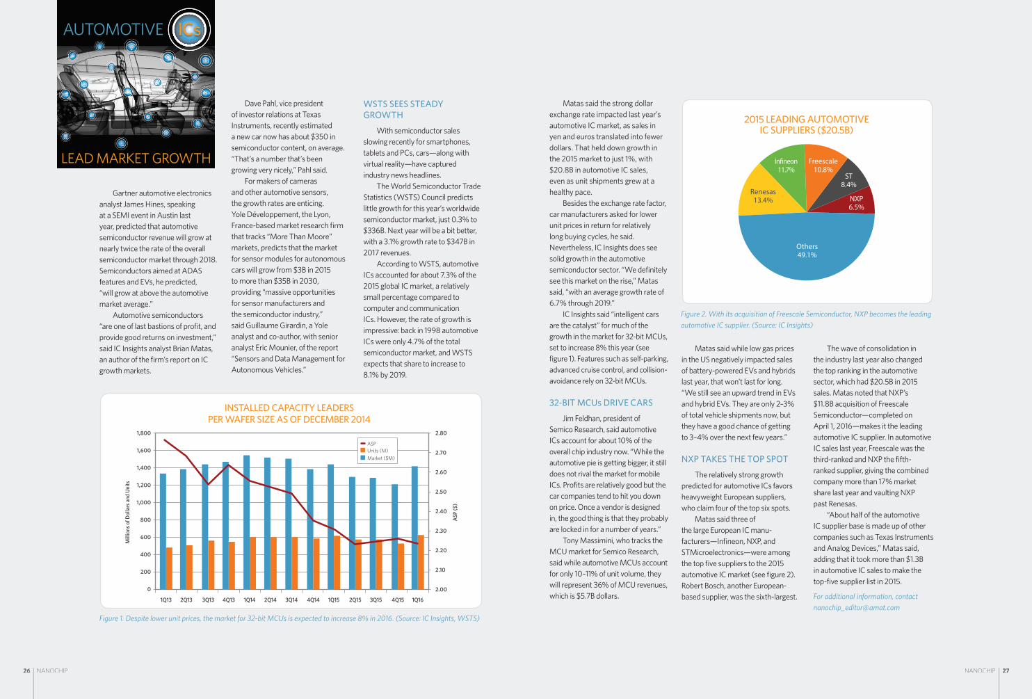
Automotive semiconductors “are one of last bastions of profi t, and provide good returns on investment,” said IC Insights analyst Brian Matas, an author of the fi rm’s report on IC growth markets.
Matas said the strong dollar exchange rate impacted last year’s automotive IC market, as sales in yen and euros translated into fewer dollars. That held down growth in the 2015 market to just 1%, with $20.8B in automotive IC sales, even as unit shipments grew at a healthy pace.
Besides the exchange rate factor, car manufacturers asked for lower unit prices in return for relatively long buying cycles, he said. Nevertheless, IC Insights does see solid growth in the automotive semiconductor sector. “We defi nitely see this market on the rise,” Matas said, “with an average growth rate of 6.7% through 2019.”
IC Insights said “intelligent cars are the catalyst” for much of the growth in the market for 32-bit MCUs, set to increase 8% this year (see fi gure 1). Features such as self-parking, advanced cruise control, and collision-avoidance rely on 32-bit MCUs.
32-BIT MCUs DRIVE CARS
Jim Feldhan, president of Semico Research, said automotive ICs account for about 10% of the overall chip industry now. “While the automotive pie is getting bigger, it still does not rival the market for mobile ICs. Profi ts are relatively good but the car companies tend to hit you down on price. Once a vendor is designed in, the good thing is that they probably are locked in for a number of years.”
Tony Massimini, who tracks the MCU market for Semico Research, said while automotive MCUs account for only 10–11% of unit volume, they will represent 36% of MCU revenues, which is $5.7B dollars.
Matas said while low gas prices in the US negatively impacted sales of battery-powered EVs and hybrids last year, that won’t last for long. “We still see an upward trend in EVs and hybrid EVs. They are only 2–3% of total vehicle shipments now, but they have a good chance of getting to 3–4% over the next few years.”
NXP TAKES THE TOP SPOT
The relatively strong growth predicted for automotive ICs favors heavyweight European suppliers, who claim four of the top six spots.
Matas said three of the large European IC manu-facturers—Infi neon, NXP, and STMicroelectronics—were among the top fi ve suppliers to the 2015 automotive IC market (see fi gure 2). Robert Bosch, another European-based supplier, was the sixth-largest.
AUTOMOTIVE ICs
LEAD MARKET GROWTH
Dave Pahl, vice president of investor relations at Texas Instruments, recently estimated a new car now has about $350 in semiconductor content, on average. “That’s a number that’s been growing very nicely,” Pahl said.
For makers of cameras and other automotive sensors, the growth rates are enticing. Yole Développement, the Lyon, France-based market research fi rm that tracks “More Than Moore” markets, predicts that the market for sensor modules for autonomous cars will grow from $3B in 2015 to more than $35B in 2030, providing “massive opportunities for sensor manufacturers and the semiconductor industry,” said Guillaume Girardin, a Yole analyst and co-author, with senior analyst Eric Mounier, of the report “Sensors and Data Management for Autonomous Vehicles.”
The wave of consolidation in the industry last year also changed the top ranking in the automotive sector, which had $20.5B in 2015 sales. Matas noted that NXP’s $11.8B acquisition of Freescale Semiconductor—completed on April 1, 2016—makes it the leading automotive IC supplier. In automotive IC sales last year, Freescale was the third-ranked and NXP the fi fth-ranked supplier, giving the combined company more than 17% market share last year and vaulting NXP past Renesas.
“About half of the automotive IC supplier base is made up of other companies such as Texas Instruments and Analog Devices,” Matas said, adding that it took more than $1.3B in automotive IC sales to make the top-fi ve supplier list in 2015.
For additional information, contact [email protected]
WSTS SEES STEADY GROWTH
With semiconductor sales slowing recently for smartphones, tablets and PCs, cars—along with virtual reality—have captured industry news headlines.
The World Semiconductor Trade Statistics (WSTS) Council predicts little growth for this year’s worldwide semiconductor market, just 0.3% to $336B. Next year will be a bit better, with a 3.1% growth rate to $347B in 2017 revenues.
According to WSTS, automotive ICs accounted for about 7.3% of the 2015 global IC market, a relatively small percentage compared to computer and communication ICs. However, the rate of growth is impressive: back in 1998 automotive ICs were only 4.7% of the total semiconductor market, and WSTS expects that share to increase to 8.1% by 2019.
INSTALLED CAPACITY LEADERSPER WAFER SIZE AS OF DECEMBER 2014
Mill
ions
of D
olla
rs an
d Un
its
1,800
1,600
1,400
1,200
1,000
800
600
400
200
0
ASP
($)
2.80
2.70
2.60
2.50
2.40
2.30
2.20
2.10
2.00
1Q164Q153Q152Q151Q154Q143Q142Q141Q144Q133Q132Q131Q13
Market ($M)Units (M)ASP
Figure 1. Despite lower unit prices, the market for 32-bit MCUs is expected to increase 8% in 2016. (Source: IC Insights, WSTS)
2015 LEADING AUTOMOTIVEIC SUPPLIERS ($20.5B)
Renesas13.4%
Others49.1%
NXP6.5%
ST8.4%
Freescale10.8%
In�neon11.7%

NANOCHIPNANOCHIP28 29
AUTOMOTIVE POWER DEVICE MARKET AMPS UP
BY BENJAMIN
LEE
Automotive power electronics are emerging as one of the semiconductor industry’s key drivers. These electronics include power devices that are at the heart of a new breed of electric vehicles (EVs) capable of going 200 miles or more between charges.
Although unit shipments of smartphones have been much higher than automobiles (1.4B[1] versus 88 million in 2015[2]), automobiles have much higher semiconductor content. Automotive power ICs are showing healthy growth, with an estimated 8% CAGR for the automotive power IC sector over the 2015–2020 period.[3] Battery-powered EVs are particularly strong drivers of the sector: a May 2015 Teardown.com report on the BMW i3 electric vehicle revealed more than 100 power-related chips in the bill of materials.
Unlike typical logic transistors that follow Moore’s Law scaling, power device FETs typically use much older technology nodes, such as 200mm (and smaller) wafers. Nevertheless, since the late 1980s power devices have continuously evolved. For example, thick PVD aluminum on the order of 3–12µm must be deposited on both the front- and backside of the device in order to provide heat dissipation and improve electrical performance. If not deposited properly, thick
aluminum can be prone to whiskers and dislocations leading to catastrophic device failure. The Applied Endura PVD HDR Al reactor ensures that such defects are minimized while providing for deposition rates that are more than 50% higher than competing technologies.
In addition, thick epitaxial silicon ranging from 5 to more than 100µm with complex dopant profi les enables low resistance (Rds), large o� -resistance (Ro� ,) and faster switching speeds.
Applied’s new Centura high growth rate epi system delivers 50–100% higher growth rates, up to a 30% reduction in chemical fl ow, shorter clean times, and lower cost of cleaning consumables (CoC) compared to conventional processes (see New High-Productivity Epi Chamber for Thick Silicon Epitaxy” on page 2 of this issue of Nanochip Fab Solutions). It demonstrates excellent within-wafer uniformity and resistivity for advanced power device needs.
Architectural changes to the semiconductor fi lm stack, such as moving the gate structure from planar (lateral devices) to trench (vertical devices), have enabled insulated-gate bipolar transistors (IGBTs) to enjoy faster switching speeds at lower losses. Similarly, for super-junction MOSFETs (SJMs), moving from multi-epi to deep trench fi ll has enabled substantial performance gains as well.
Some improvements and adjustments to etch processes have been necessary to accommodate these schemes, which involve higher aspect ratio structures. Improved epi Si fi lms and optimized implant doping profi les also have enabled performance gains.
Power device manufacturers continue to look for more improvements. According to publicly available reports, Hitachi’s high-conductivity IGBT employs a separate fl oating p-layer to improve gate controllability and turn-on voltage. ABB Semi is creating P-pillar implants under the trench gates to create a super-junction e� ect to enable higher switching speeds.
Wafers are being thinned across the board to help reduce stored charge for high-speed switching. Fuji Electric has recently developed a seventh-generation IGBT with a thinner drift layer, smaller trench pitch, and optimized fi eld-stop layer.
However, the consensus among experts is that the performance envelope for silicon devices has been pushed nearly to the limit. Power devices are limited by intrinsic silicon properties, so each subsequent stage of progress provides only marginal improvements.
III-V POWER DEVICESThe power IC industry is
looking to new wide bandgap (WBG) materials to take performance to an entirely new level. Silicon carbide (SiC) and gallium nitride (GaN) are the top candidates today, each with their own set of pros and cons. These are compound semiconductor materials that provide much higher bandgap and breakdown fi elds, taking power device performance to a level where silicon simply cannot compete. They are widely considered to herald the next era of power devices, the next big infl ection.
WBG – SiC vs. GaN DEVICE POSITIONING
PFC/Power Supply
LOW VOLTAGE MEDIUM VOLTAGE
Audio Amplifier
PV Inverter
EV/HEV
Motor Control
UPS
Smart Power Grid
Rail Transport
HIGH VOLTAGE
Ships & Vessels
Wind Mills
<200 V 600 V 900 V 1.2 k V 1.7 kV 3.3 k V 6.5 kV+
GaN/SiCOverlap
SiCMed – High Voltage
GaNLow – Med Voltage
Figure 1. Wide bandgap power devices have advantages for EVs and other systems, but materials costs are a challenge. (Source: Yole Développement and Applied Materials)

NANOCHIPNANOCHIP30 31NANOCHIP 31
Inline inspection based analytical techniques adapted from high-volume semiconductor manufacturing can help manufacturers of low-temperature polysilicon (LTPS) LCD and fl exible OLED displays. During production ramp-up, the use of a new technology under development at Applied Materials —electron beam review (EBR)—will enable display manufacturers to achieve optimum yields faster than traditional methods, allowing them to capture millions of dollars in revenue and avoid costly yield excursions.
INLINE SEM ELECTRON BEAM REVIEW
BY KERRY CUNNINGHAM
Table 1: Both GaN and SiC have superior bandgap and breakdown properties compared with today’s silicon-based power devices. (Source: F. Iacopi, et al, MRS Bulletin, May 2015; courtesy of Jim Plummer, PhD, Stanford University)
MATERIAL PROPERTIES: SILICON VS. NEW MATERIALS
Si GaAs GaN 4H-SiC
Bandgap energy (eV) 1.12 1.4 3.49 3.26
Breakdown fi eld (MV/cm) 0.3 0.4 3.5 3
Electron mobility at 300 K (cm2/V-s)
1400 8500* 10,000
900* 2000
700
Saturated (peak) electron velocity (107 cm/s)
1.0 (1.0) 1.3 (2.1) 1.3 (2.7) 2.0 (2.0)
Relative dielectric constant 11.8 12.8 9 10
Thermal conductivity (W/cm-K) 1.5 0.5 1.7 3.5
Thermal expansion (10-6/K) 2.6 5.7 5.6 5.1
Lattice constant (Å) 5.43 5.65 3.19 3.07
* Values of corresponding heterostructures
Infl ections bring new challenges, and WBG power ICs are no exception. Cost is the biggest obstacle today, including manufacturing-related challenges from wafer warpage and high rates of defects associated with substrate and epitaxial processing. Currently, a 6-inch SiC substrate + epi wafer costs in the thousand-dollar range, according to market research fi rm Yole Développement (Lyon, France). And that cost can multiply quickly with more stringent device defect requirements.
There are other challenges in subsequent process fl ow steps. For example, high-temperature anneals nearing the 2,000°C range are required. Typical anneal reactors for Si come nowhere near this regime. Implanting into SiC is also quite complex.
Encouraged by the potential of WBG power devices, several companies, consortia, and university research centers are focused on solving their challenges. In fact, both
SiC and GaN products are available today, albeit in limited quantities. However, costs must come down signifi cantly before the benefi ts of WBG—including power savings, simplifi ed circuitry, and reduction in module size—can provide a meaningful return on investment compared to silicon substrates.
Take, for example, a typical automobile inverter box that may contain 40 or more power transistors and diodes. Moving to SiC enables simplifi ed circuitry, fewer components, and an overall module size reduction of up to 80%. It is this intersection of device size, materials cost, and energy savings that must be satisfi ed to create a meaningful value-add compared to silicon power devices (see table 1).
Fortunately, other steps in the semiconductor processing fl ow, such as CVD, PVD, etch and CMP, are relatively straightforward for WBG power devices because the general process fl ow is very similar to that of silicon. Process tuning is required along with minor hardware changes, but existing technologies can be adapted to WBG processing.
GaN-based power devices have great potential for high-voltage automotive applications, but GaN
brings its own list of challenges, including wafer costs and e� ective production of GaN-on-GaN structures (a bulk GaN substrate with GaN epi). Only 2-inch bulk GaN wafers are available today. Moreover, with current architectural limitations, GaN devices are normally ON, which introduces reliability issues and limits market acceptance. Enhancement-mode GaN devices would be needed to overcome this shortcoming. Therefore while the performance benefi ts of WBG devices are undeniable, it is an open question whether they can overcome the cost challenges and achieve high volumes.
In a recent power device seminar at Applied Materials, Stanford University Professor Jim Plummer suggested that for these devices to achieve success in the marketplace, it would make sense to identify a new space where silicon doesn’t compete. This would enable increases in manufacturing volume, which Plummer said would then help reduce wafer costs.
For additional information, contact [email protected]
[1] Source: IDC report 2015[2] Source: KPMG report 2016[3] Source: PWC Report 2015
AUTOMOTIVE POWER DEVICE MARKET AMPS UP
ACCELERATES LTPS DISPLAY YIELD RAMPS

NANOCHIPNANOCHIP32 33
AOI Defect Map (in line) Break Glass for SEM Review Send to FA SEM
Analyze
Lostinformationand scrap
CycleStarts
Last SampleBefore
Excursion
ExcursionOccurs
First SampleAfter
Excursion
ExcursionDetected
SourceIdentified
SourceEliminated
EBR Reduces Yield Excursion Correction Time
Yield Excursions
Yield Entitlement
TimeSystemFab-in
Setup Pilot Pre -MP MP
YIELD
YIELD W/ EBR
PARTICLE DENSITY
3
2
Ramp to Yield1
Part
icle
Den
sity
Yiel
d
Combining state-of-the-art scanning electron microscopy (SEM) with large-scale display vacuum platforms, EBR is a new approach that can shave several months from the average LTPS display fab ramp time of 15 months (see fi gure 1). Assuming a factory output of 30,000 displays/month, a 3-month savings for example, would be equivalent to $250 million in added revenue.
Applied Materials is developing inline EBR technology (see fi gure 2) as a better, faster way to discover and address the root causes of killer defects in mobile display production, which is characterized by an increasing number of process steps that can generate more—and smaller—particles and new types of defects.
Killer defects, or electrically active faults, destroy pixels and reduce yield. It can be di� cult to determine their origin because while they may result from a straightforward one-time issue, they also may be symptomatic
of a problem with a tool or process that negatively impacts yields on an ongoing basis.
Consider the example of a cluster defect that a� ects 10 displays out of 250 (a 4% yield loss). It would be wrong to say that the cluster is a systematic defect, because the cluster is just the location and not the root cause. The root cause could be a mask defect, a defective sputter target, etc. Thus, the goal is to determine the systematic root cause, which will fi x not only the 4% yield loss issue but also other issues that may manifest themselves in di� erent locations but share the same root cause.
While inline automated optical defect inspection tools can detect the location of defects on a sample substrate, they simply report all visually abnormal regions, both killer defects and also nuisance or non-killer defects. Prior to EBR, in order to do SEM analysis, the substrate had to be broken into pieces and each piece examined separately under microscope (see fi gure 3). Although such
o� ine SEM analysis does enable root-cause analysis, a crucial linkage is lost by having to break the substrate into pieces: it’s impossible to compare the inline defect to an end-of-line array test, because the defect location on the full panel can no longer be determined.
As a result, insight into the source(s) and kill ratio of the defects is lost, making discovery a problematic and time-consuming process. Using EBR, however, it is possible to
determine which defects are killer defects without breaking the substrate for analysis.
Moreover, because production continues while random samples are inspected, any lots that have been processed during that time may su� er from the same problem and have to be scrapped.
MINIMIZE KILLER DEFECTS IN REAL TIME
To address these issues, Applied Materials has introduced an analytical approach based on EBR technology that will help LTPS display manufacturers minimize killer defects in real time when a process or tool is not performing to specifi cations (see fi gure 4).
EBR makes use of both optical imaging analysis and SEM/energy-dispersive X-ray (EDX) tools. It can handle LTPS panels up to Generation 6 (1850mm x 1500mm) with no need to break them into Figure 1. Excursion management improves fab ramp time and overall yield.
Figure 2: Applied Materials EBR platform.
Figure 3. In conventional LTPS display manufacturing, LTPS panels have become so large that in order to inspect one using a SEM tool it must be broken into pieces and each piece examined separately. Crucial information that may give insight into the source(s) of the defects is therefore lost.
pieces. The overall approach is to isolate the most probable source of a defect (e.g., a CVD, PVD, etch, photolithography, or other process step), select the best sampling plan to isolate and monitor the defect, and then quantify the number of lots impacted.
Sample substrates are inspected after each process
step. Automated optical inspection is used to generate a map of defects on these wafers. The wafers are then reviewed with the EBR SEM tool, and the results of that inspection are overlaid with the results of the optical inspection so that the EBR results can be analyzed to determine the composition and size of the defects (see fi gures
Figure 4. Yield excursion identifi cation and correction cycle. (Source: AKT)
5 and 6). These tests can and should be repeated after each process step.
A focused electron beam stimulates atoms in the sample with uniform energy. The atoms instantaneously send out X-ray radiation in characteristic signatures unique to each element, as shown in the graph. These give information about
the elemental composition of the sample. Chemical elements starting with the atomic number 4 (Be) can be identifi ed this way.
This information will enable users to “work backward” from the defect to determine where it is coming from so that the problem can be fi xed quickly. In this way, the tool or process step that is most likely to be
INLINE SEM ELECTRON BEAM REVIEW
ACCELERATES LTPS DISPLAY YIELD RAMPS
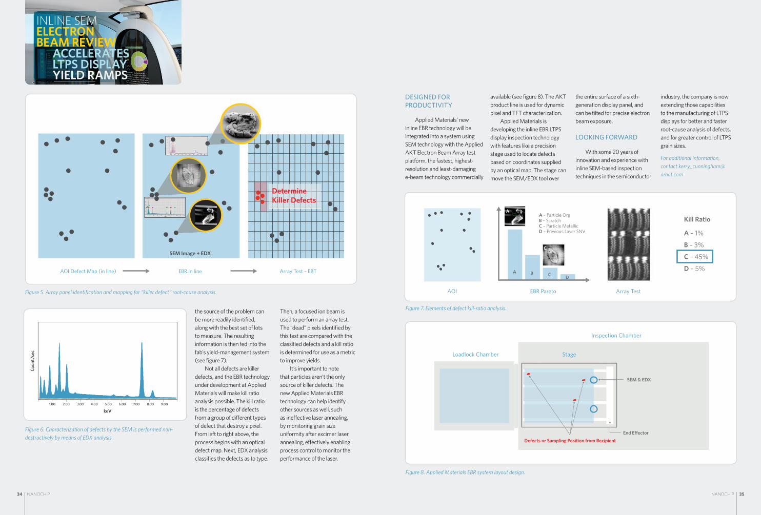
NANOCHIPNANOCHIP34 35NANOCHIP34 NANOCHIP 35
Loadlock Chamber
Inspection Chamber
Stage
SEM & EDX
End E�ectorDefects or Sampling Position from Recipient
AOI EBR Pareto Array Test
A – Particle OrgB – ScratchC – Particle MetallicD – Previous Layer SNV
A B C D
A
C
Kill Ratio
A – 1%
B – 3%
C – 45%
D – 5%
Coun
t/sec
1.00 2.00 3.00 4.00 5.00 6.00 7.00 8.00 9.00
keV
AOI Defect Map (in line) EBR in line
SEM Image + EDX
Array Test – EBT
DetermineKiller Defects
the source of the problem can be more readily identifi ed, along with the best set of lots to measure. The resulting information is then fed into the fab’s yield-management system (see fi gure 7).
Not all defects are killer defects, and the EBR technology under development at Applied Materials will make kill ratio analysis possible. The kill ratio is the percentage of defects from a group of di� erent types of defect that destroy a pixel. From left to right above, the process begins with an optical defect map. Next, EDX analysis classifi es the defects as to type.
Figure 6. Characterization of defects by the SEM is performed non-destructively by means of EDX analysis.
Figure 5. Array panel identifi cation and mapping for “killer defect” root-cause analysis.
Then, a focused ion beam is used to perform an array test. The “dead” pixels identifi ed by this test are compared with the classifi ed defects and a kill ratio is determined for use as a metric to improve yields.
It’s important to note that particles aren’t the only source of killer defects. The new Applied Materials EBR technology can help identify other sources as well, such as ine� ective laser annealing, by monitoring grain size uniformity after excimer laser annealing, e� ectively enabling process control to monitor the performance of the laser.
DESIGNED FOR PRODUCTIVITY
Applied Materials’ new inline EBR technology will be integrated into a system using SEM technology with the Applied AKT Electron Beam Array test platform, the fastest, highest-resolution and least-damaging e-beam technology commercially
available (see fi gure 8). The AKT product line is used for dynamic pixel and TFT characterization.
Applied Materials is developing the inline EBR LTPS display inspection technology with features like a precision stage used to locate defects based on coordinates supplied by an optical map. The stage can move the SEM/EDX tool over
Figure 8. Applied Materials EBR system layout design.
Figure 7. Elements of defect kill-ratio analysis.
the entire surface of a sixth-generation display panel, and can be tilted for precise electron beam exposure.
LOOKING FORWARD
With some 20 years of innovation and experience with inline SEM-based inspection techniques in the semiconductor
industry, the company is now extending those capabilities to the manufacturing of LTPS displays for better and faster root-cause analysis of defects, and for greater control of LTPS grain sizes.
For additional information, contact [email protected]
INLINE SEM ELECTRON BEAM REVIEW
ACCELERATES LTPS DISPLAY YIELD RAMPS

NANOCHIPNANOCHIP36 37
The fabrication of advanced gate stacks and complex device geometries increasingly depends on new processes, chemistries and materials that generate substantial volumes of hard-to-treat and potentially dangerous waste byproducts in chamber e� uent.
AERIS-S TECHNOLOGY: INCREASE SUBFAB SAFETY,
REDUCE EMISSIONSBY
ANDREAS NEUBER, MICHAEL COX, JOHN
DICKINSON, JIM L’HEUREUX
AND DUSTIN HO
High-aspect-ratio processes (HARP) and “dirty” chemistries—such as fl owable CVD (FCVD) based on low-thermal-budget chemical reactions—generate large volumes of byproducts that can clog forelines, gate valves and pumps. Meanwhile, low-material-e� ciency processes such as atomic layer deposition (ALD) deposit only a small fraction of the gaseous source material onto the wafer; the rest must be removed from the waste stream. Finally, SiGe, III-V, and other alternative materials and highly reactive precursors may pose safety and operational concerns if they are energetic, pyrophoric or toxic to humans, as many are.
This means it is no longer enough to simply meet governmental emissions regulations, despite how di� cult that can be under these new manufacturing conditions. To be successful in today’s hyper-competitive markets, semiconductor manufacturers must place greater emphasis on hazardous material management when treating chamber e� uent so that subfab utilities and subsystems remain safe, available, cost-e� ective and e� cient—even under heavy factory loads.
Applied Materials is now developing a promising solution for these challenges: Applied Aeris-S abatement technology.
Figure 1. The Aeris-G pre-pump plasma abatement system enables semiconductor manufacturers to meet greenhouse gas (GHG) reduction goals with no added subfab footprint required. The new Aeris-S system is a pre-pump, magnetically confi ned, capacitively coupled plasma source used to address environmental, health and safety concerns with CVD and other advanced processes. Aeris-S also helps manage solids accumulation and tool productivity.
AERIS-S
AERIS-G
This new solution operates by converting problematic materials into compounds that can be managed and transported more easily and safely for abatement (either locally or in the central scrubber). Aeris-S technology also improves subfab safety by reducing the levels of fl ammable, explosive or toxic exhaust gases and the accumulation of potentially hazardous reactive solids downstream of the chamber.
Initially focused on HARP applications, the new Aeris-S technology is currently undergoing beta testing at a number of fabs. The system builds on the success of the Applied Aeris-G pre-pump plasma abatement system, some 2,000 of which are installed at fabs worldwide. Using Aeris-G units has enabled fabs to meet increasingly strict emissions regulations and reduce their carbon footprints while maximizing system uptime and reducing overall costs.
Like the zero-footprint Aeris-G units, the new Aeris-S units sit in the existing pump footprint for each chamber but are placed before the pump so they can treat the actual process gas volume, a much smaller and more concentrated gas volume than what is treated by traditional post-pump abatement technology (see fi gure 1).

NANOCHIPNANOCHIP38 39
AERIS-S TECHNOLOGY INCREASE SUBFAB SAFETY, REDUCE EMISSIONS
However, Applied’s Aeris-S technology brings powerful capabilities to the more challenging abatement requirements at the leading edge of semiconductor manufacturing. For example, the Aeris-G and Aeris-S technologies employ di� erent plasma sources.
Existing Aeris-G units use an inductively coupled plasma source to actively manage process e� uent and reduce solids accumulation. This is a more e� ective solution than passive microwave-based pipe-heating and post-pump purging systems. Aeris-G units virtually eliminate volatile organic compounds (VOCs) and COx from tool exhaust because no fuel is used. They also eliminate NOx emissions because e� uent is treated before it is diluted with N2 purge gases. Aeris-G technology
demonstrates typical destruction removal e� ciencies (DRE) greater than 99% for SF6, CHF3, C3F8, NF3 and C4F8, and greater than 95% for CF4.
By contrast, Applied’s new Aeris-S technology employs a higher-power magnetically confi ned and capacitively coupled plasma source to dissociate complex molecules, and precipitate and evaporate solids. It features high fl ow rates (100 slm) and a wide operating range. These features allow users to manage and prevent accumulation of solids in and beyond the foreline, increasing uptime and availability and reducing costs. In addition, these features drive reactions that turn harmful compounds into less harmful ones, reducing potential risks to maintenance personnel.
STEP 1
Aeris-S completes the TEOS oxidation
INCO
MIN
G T
EOS
TEOS BREAKDOWNON WAFER
AND CHAMBER
WASTE STREAM:• Teos Si(OC2H5)4• CO• HCOOH• CO2• CH4
SiO2
CO
CO2
NO
NO2
Deposits atAeris-S shieldsand cooled foreline
Pump neutralgaseouse�uents
Figure 2. Illustrations show that Aeris-S abatement technology fi rst turns TEOS e� uent into “cleanable” SiO2 (step 1), and then turns the SiO2 into SiF4 (step 2), which is easy for a scrubber to remove from a fab’s waste stream.
STEP 2
Aeris-S activates F2 andconverts solid SiO2 into SiF4
INCO
MIN
G N
F 3
F RADICALS CONVERTSiO2 INTO SiF4
F RADICALSRECOMBINE ANDDO NOT REACT
ANYMORE
SiF4
CO2
COF2
HF
CF4
Pump neutralgaseouse�uents
Pump neutralgaseouse�uents
SiF 4
(SCC
)
321
SiF4 Emission During Clean Process
AERIS-S ONAERIS-S OFF
Figure 3. Aeris-S technology reactivates F2 to F radicals and thereby converts SiO2 to SiF4. The concentration of SiF4 in chamber e� uent can be used as an indicator of cleaning e� ciency, because more SiF4 in the e� uent means that more SiO2 has been converted. The fi gure captures data from three tests, showing twice the SiF4 emission levels with Aeris-S technology.
Results from the beta tests indicate that Aeris-S technology can e� ectively treat high volumes of e� uents with a wide range of chemistries and foreline pressures. It can signifi cantly lengthen preventive maintenance (PM) intervals for pumps and post-pump abatement equipment, and improve subfab safety by reducing hazardous levels of exhaust gases and downstream accumulations of reactive solids.
Both Aeris-G and Aeris-S units are synchronized with chamber operation and operate on-demand. This can lower the overall utility cost of ownership by up to 70%.
HOW IT WORKS
To more clearly illustrate the working principle of Aeris-S technology, consider a HARP process that incorporates a TEOS deposition step. The waste stream from TEOS breakdown on the wafer and in the chamber comprises the following molecules: TEOS, which is Si(OC2H5), along with CO, HCOOH, CO2 and CH4. (See fi gure 2, step 1.)
TEOS and its byproducts are toxic or fl ammable and the goal is to eliminate them from the waste stream. Applied’s Aeris-S technology performs a two-step process to eliminate TEOS during the cleaning process. First, the Aeris-S converts it into SiO2, which is much easier to handle and is deposited on the pump shields and in the foreline.
Second, NF3 is introduced into the Aeris-S system as a source of highly reactive fl uorine radicals (fi gure 2, step 2). The Aeris-S activates the NF3. Some of the F radicals recombine and don’t react anymore, but some of them convert the SiO2 into SiF4. This removes the SiO2 buildup, and leaves SiF4, which a fab’s central scrubber can manage easily.
The concentration of SiF4 in the e� uent can be seen as an indicator of cleaning e� ciency (i.e., more SiF4 in the e� uent means that more SiO2 e� uent has been converted). The removal e� ciency of Aeris-S units in beta tests is shown in fi gure 3.
Applied’s new Aeris-S technology is designed for low operating costs and has a fl exible architecture for easy cleaning and maintenance. The units are externally programmable to control reagent fl ow, power and purge functions, and can interface with production tools from Applied Materials or other manufacturers, as well as a fab’s host computer system.
It is always Applied Materials’ goal to have increased uptime, higher e� ciency and lower operating costs go hand-in-hand with good environmental stewardship and safe operating practices. The new Applied Aeris-S technology will help ensure that customers continue to enjoy those benefi ts no matter how complex semiconductor fabrication becomes.
For additional information, contact [email protected]

NANOCHIPNANOCHIP40 41NANOCHIP 41
Ah, there is nothing like the future of Moore’s Law scaling to get the blood boiling, and the discussions at the recent Advanced Semiconductor Manufacturing Conference (ASMC 2016) in Saratoga Springs, New York were especially lively.
Dick James, senior fellow at ChipWorks, set the stage with a slide show of the leading-edge ICs his company has dissected recently. His talk—appropriately titled “Moore’s Law Continues Into the 1x-nm Era”—was worth the price of ASMC admission. Interestingly, James said that the FinFET-based devices ChipWorks has studied are remarkably the same, with roughly the same 40nm fi n height. The FinFETs, which have all appeared in commercially available processors, showed “quite a bit of commonality,” he said, noting that Intel’s 14nm transistor does have a smaller gate length (22nm) than comparable devices from two foundries (28–30nm).
James also made an important point: in recent technology generations, the leading-edge chips have succeeded in a roughly 50% areal shrink for the SRAM bit cells. At an ASMC panel discussion on the economics of Moore’s Law, Intel executive David Bloss expanded on the importance of the areal shrink. Without the ability to shrink the transistors for a “given amount of money,” he said,
the economics of moving to the next technology node fall apart.
“If we don’t get the traditional [areal] scaling, this could break Moore’s Law,” said Bloss.
When Robert Maire, president of Semiconductor Advisors, asked the panelists if they agreed that the cost-per-transistor had fl attened out beyond the 28nm node, Qualcomm’s Senior Director of Engineering William Miller begged to di� er. “We might have seen a little bump in the road, but I think Moore’s Law scaling is solid to 7nm, and I would never say never about 5nm. I do believe it will continue, though 5nm might be di� cult.”
Both Intel’s Bloss and Qualcomm’s Miller said the market will demand more highly integrated chips. By 2019, Miller predicted, 90% of all phones will be smartphones, and many
of them will be based on octi-core processors. Bloss said those phones and all manner of other things will be constantly feeding data to the cloud, which will spur demand for processors.
“There will be massive data processing in the cloud. So much data will become available in the next fi ve years, I can’t imagine smart people not trying to analyze and use that data,” said Bloss.
Patrick Martin, head of fi eld technology at Applied Materials, said EUV is “mandatory” for successful scaling, especially for scaling the back-end-of-the-line (BEOL) interconnects. “EUV would take a lot of the cost out” and “play a role in [reducing] yield loss,” Martin said.
Qualcomm’s Miller put a lot of emphasis on packaging, especially system-in-packages (SIPs) and fan-out wafer level packaging, either of which will allow Qualcomm to combine several chips “in a quarter-sized package.”
Two technical papers at ASMC 2016 stand out in my mind. And they both have a tangential relation to Moore’s Law.
One was presented by Christopher Carr, an Intel lithographer working at the Global 450mm Consortium in Albany, New York. Carr and his coauthors from Nikon Precision were forthright about the engineering challenges involved in getting Nikon’s 450mm immersion, 193nm-wavelength scanner up to the overlay and other tool acceptance standards set by the 450 consortium.
A second notable paper that discussed through silicon via (TSV) process developments came from a team of GLOBALFOUNDRIES engineers. They noted that if packing in more transistors becomes problematic, the industry is likely to rev up its investments in 3D TSVs and 450mm manufacturing.
Carr said a 450mm wafer contains 212 “fi elds” compared with 96 comparable exposures on a 300mm wafer, holding out the promise of a 30% gain in return on investment (ROI) from the larger platters.
However, James Moyne, a professor at the University of Michigan said, “the semiconductor industry is no longer mainly about computing. There is a lot more going on in MEMS sensors and other devices which do not rely on advanced design rules. The industry is broadening out.”
ASMC 2016 showed plenty of ideas about how to gain cost-per-function improvements, which are, at the bottom line, the heart of Gordon Moore’s amazing prediction.
David Lammers is an Austin-based technology journalist.
THE
LAST
WO
RD
DAVID LAMMERS
NEVER SAY NEVER TO MOORE’S LAW
William Miller, Senior Director of Engineering, Qualcomm
David Bloss, Vice President, Technology & Manufacturing Group; Director, Fab Equipment Supply Chain, Intel
Robert Maire,President of Semiconductor Advisors, LLC
Customers covered by Applied’s Managed- or Performance Service Agreements already receive PM services as an integral part of their support programs. In addition, for those who are covered only by Applied’s new product warranty or Standard Service Agreement, there is now an option for routine preventive services as well.
New Applied PM Services o� er customers the expertise, convenience, e� ciency and a� ordability they need to keep their Applied Materials equipment operating at peak performance. For warranty customers, PM is an important way to rapidly achieve predictable, repeatable levels of performance at the best cost. Standard Service customers benefi t as well from regular, state-of the-art PM services that use the latest tools, techniques and service routines.
Applied PM Services are delivered at scheduled intervals by specially trained Applied Materials TechForce personnel− certifi ed service technicians, who perform PM tasks on process chambers,
wafer-handling systems and the factory interfaces. They ensure that everything needed for specialized PM tasks, including parts kits, high-quality consumables and specifi c process kits, is on hand for the scheduled PM service. Included in the product o� ering are the additional process kits required during the chamber clean. These support the rapid return to production made possible by swapping cleaned and refurbished parts for used ones. Under a PM Services contract the process kits are inspected, cleaned and refurbished to like-new condition, or parts are replaced as needed as part of the program.
Applied works with customers to develop a rolling schedule for PM service that conforms to the customer’s unique operating practices and production needs. The delivery of PM services is fl exible enough to provide for PM to be performed within eight hours of a customer’s request to address an unplanned event.
With Applied PM Services, customers benefi t whether they are running advanced processes on state-of-the-art tools that require knowledge of new cleaning methods, or doing older processes in greenfi eld fabs, even in geographic areas where the technical support infrastructure may be limited.
Applied PM Services o� er First Time Right performance: Applied’s assurance of consistently high-quality service. The goal is to minimize scheduled downtime through repeatable task performance. This means that if the initial chamber requalifi cation process is unsuccessful and attributable to an improperly performed PM, Applied will support the subsequent e� orts to successfully recover and return the chamber to production status. Applied o� ers this service at a cost savings over standard transactional services that include parts procurement, cleaning, and materials management tasks as required to sustain predictable operation.
This level of support is made possible by Applied’s extensive global parts infrastructure and e� ciencies, and by the high level of training provided to fi eld service technicians, most of whom are local to customers’ fabs. For example, Applied’s Tech Guides training team uses virtual reality simulations and other advanced teaching methods to bring our trainees “inside the chamber” and optimize their understanding of Applied Materials hardware and proprietary technologies.
The combination of greater parts e� ciencies and expert sta� training helps customers reduce the costs and risks that stem from improperly performed PM tasks, which can arise from errors in workmanship or poor-quality parts that prevent chamber recovery to production status. It also frees up a fabs’ own service technicians for other tasks.
Applied Materials has demonstrated that it can deliver repeatable, predictable and fast results using a methodological approach to PM execution based on industrywide best practices, intimate tool and process knowledge, and high-quality parts and parts-cleaning practices.
Thus, customers who contract for the new Applied PM Services option can expect to achieve greater tool stability and availability, and to benefi t from more predictable operating costs.
For additional information, contact [email protected]
Preventive maintenance (PM) can maximize tool availability and minimize the risk of sudden increases in operating costs—provided it is timely and e� ective. Data from Applied Materials
Managed Service Agreements shows that tools which receive appropriate PM according to Applied’s guidelines
demonstrate an average improvement in scheduled uptime in the range of 3–5% over those which do not.
NEW PREVENTIVE MAINTENANCE
SERVICE OPTION
BYJOHN
DEWITT

www.appliedmaterials.com
Printed on Recycled Paper
AGS-NFS-0716 7/16 1.0K


![NANOCHIP - Applied Materials · solve growing performance issues besetting 2D scaling. This paradigm shift ... (SPM), RTP2]. Se was implanted after the wet strip, but before RTP2.](https://static.fdocuments.us/doc/165x107/5e6baed9d87b701dbd684b03/nanochip-applied-solve-growing-performance-issues-besetting-2d-scaling-this-paradigm.jpg)