NANOCHIP - Applied Materials · 2014-01-24 · 5 Volume 12, Issue 1, 2014 Nanochip Technology...
24
volume 12, issue 1, 2014 NANOCHIP Technology Journal IN THIS ISSUE • Fin Doping With Hot Implant • Plasma Doping of High Aspect Ratio Structures • Integrating Millisecond and Spike Anneals EXTENDING TRANSISTOR TECHNOLOGIES IN THE 3D ERA
Transcript of NANOCHIP - Applied Materials · 2014-01-24 · 5 Volume 12, Issue 1, 2014 Nanochip Technology...

volume 12, issue 1, 2014
NANOCHIPTechnology Journal
IN THIS ISSUE• Fin Doping With Hot Implant
• Plasma Doping of High Aspect Ratio Structures
• Integrating Millisecond and Spike Anneals
EXTENDINGTRANSISTOR TECHNOLOGIESIN THE 3D ERA

This issue of Nanochip focuses on advances and innovations taking place in front-end-of-line processes as the
transition to 3D device architecture gathers momentum and planar scaling pushes its boundaries. A primary
catalyst of change is the FinFET, whose design poses diverse challenges for gap fill, CMP, implant, metal deposition,
capacitance control, contact resistance, and channel mobility enhancement. Our feature article reviews these and
solutions already in place or under development.
We also review two advances in ion implantation. One approach employs hot implantation to solve the issue of
crystallinity damage in narrow fins that exacerbates junction leakage and parasitic resistance. A higher substrate
temperature during implantation enhances defect annihilation during the subsequent anneal, thereby raising the dose
threshold for the onset of amorphization. In other applications, plasma doping is addressing challenges posed by
high aspect ratio (HAR) features in advanced memory and CMOS image sensor devices. The inherent conformality
and tunability of plasma doping are major advantages over other approaches in applications such as HAR staircase
contacts. This technology also solves the issue of reducing dark current for CMOS image sensor manufacturers as
the lower energy levels used in plasma doping avoid the end-of-range damage responsible for this undesirable effect.
While emerging 3D solutions are claiming much of the industry’s attention, innovations continue to enhance
the performance of planar devices. We demonstrate that integrating laser millisecond anneal and spike anneal
achieves optimum dopant activation while preserving ultra-shallow junction profile and depth. The low stabilization
temperature of laser millisecond anneal precludes formation of dopant-deactivating interstitials. The spike anneal
can thus achieve maximum effect, which in turn enhances transistor drive current.
These studies are representative of our commitment to pushing the frontiers of our knowledge in pursuit of
cost-effective solutions to our customers’ high-value problems. We trust you will find them of interest and value.
Cover: The FinFET structure avoids short-channel effects that are limiting planar device scalability and eases the
power vs. performance tradeoff. While leading the industry into the 3D era, the FinFET is helping to shift the design
paradigm from packing density to best performance per watt.
TO OUR READERS

TABLE OF CONTENTS 3 Extending Transistor Technologies
in the 3D Era
9 Fin Doping With Hot Implant
for 14nm Technology and Beyond
14 Plasma Doping of High Aspect Ratio Structures
19 Integrating Millisecond and Spike Anneals
to Optimize Dopant Activation

3 Volume 12, Issue 1, 2014 Nanochip Technology Journal Applied Materials, Inc.
Extending Transistor Technologies in the 3D Era
KEYWORDS
Capacitance
Channel Mobility
CMOS
Contact
FinFET
High-κ Metal Gate
Implant
Junction
Spacer The modern MOSFET era has undergone numerous changes in transistor materials and fabrication, a trend expected to accelerate from the 2x nm node onward to satisfy growing demands for mobility and connectivity. Power economy, and greater speed and packing density are the predominant factors driving today’s transistor scaling and design innovations. This companion article to the Volume 11, Issue 1, 2013 overview of interconnect advances examines specific challenges faced by transistor technologies and solutions for their continued scaling.
Since the introduction of planar IC process technology, feature size and density have scaled at a rate of approximately 30% linear reduction per generation. This scaling has provided many benefits, including continuous cost reduction, performance improvement, and power reduction for IC technology and related products. At each generation, the industry has surmounted technology challenges to enable the scaling.
Over the last several nodes, in addition to scaling, significant changes have been made in materials and architecture used to fabricate transistors. The 90nm node saw epitaxial SiGe source drain (S/D) stressors;[1] the 45nm node saw adoption of high-κ metal gate (HKMG);[2] while 22nm introduced the non-planar FinFET[3] and ushered in the era of 3D transistors for logic. These tri-gate or FinFET transistors improve electrostatic control of the channel region, reducing off-state leakage, and enabling continued gate length scaling and greater transistor density.
The CMOS industry has made great progress in gate length (Lg) scaling, averaging 28% per generation from
the micron scale to 65nm.[1,2,4,5] In practice, Lg has scaled
at a slightly slower rate than the overall device pitch
reduction of 30%; as a result, the contact and spacer width
have scaled at a slightly faster rate. However, Lg scaling
stalled at the 45nm and 32nm nodes, primarily because
of difficulty maintaining threshold voltage (Vth) control
at short Lg. At shorter Lg, the gate and drain compete
for control of the channel, leading to a Vth
degradation
known as drain-induced barrier loading (DIBL) at higher
drain bias (Equation 1).[6] DIBL is improved if gate oxide
capacitance increases or junction depth decreases. It
degrades from lower Lg and reduced Ɛsc (dielectric
constant of the semiconductor). Despite the introduction
of HKMG, progress in DIBL improvement stalled after
45nm due to physical challenges in doping and gate
oxide thickness reduction.
[1]
DIBL = 0.80 𝜀𝜀𝑠𝑠
𝜀𝜀oxEI × 𝑉𝑉ds
EI = (l +𝑋𝑋𝑗𝑗2𝐿𝐿el2
) 𝑇𝑇ox_el𝐿𝐿el𝑇𝑇dep𝐿𝐿el
DIBL can be improved, however, by using a multi-gate
device, which increases gate coupling to the channel and
effectively makes the junction depth shallower. In the
planar device, a capacitor lies between the gate and the
channel and between the drain and the channel (Figure 1a).
These two capacitors compete to control the channel
potential. As the gate must remain in control, the ratio
of gate and drain capacitance must be controlled. FinFET
topography adds multiple gates on the side of one
channel (Figure 1a), improving the gate coupling ratio.
This can be thought of as effectively reducing the junction
depth to half the fin width (Wfin). Thus, the FinFET can
be scaled by reducing the Wfin
for each generation as
Lg is also reduced.[7] Although the FinFET is a practical
way to fabricate double gate devices on a silicon wafer,
it introduces many new challenges, including pitch
scaling and conformality, and complex topological
requirements (Figure 1b).
4Volume 12, Issue 1, 2014Nanochip Technology JournalApplied Materials, Inc.
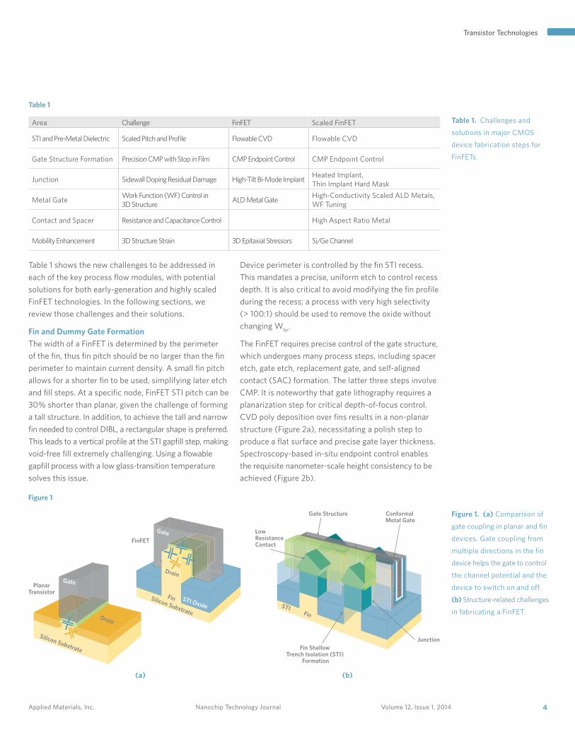
Table 1 shows the new challenges to be addressed in
each of the key process flow modules, with potential
solutions for both early-generation and highly scaled
FinFET technologies. In the following sections, we
review those challenges and their solutions.
Fin and Dummy Gate Formation
The width of a FinFET is determined by the perimeter
of the fin, thus fin pitch should be no larger than the fin
perimeter to maintain current density. A small fin pitch
allows for a shorter fin to be used, simplifying later etch
and fill steps. At a specific node, FinFET STI pitch can be
30% shorter than planar, given the challenge of forming
a tall structure. In addition, to achieve the tall and narrow
fin needed to control DIBL, a rectangular shape is preferred.
This leads to a vertical profile at the STI gapfill step, making
void-free fill extremely challenging. Using a flowable
gapfill process with a low glass-transition temperature
solves this issue.
Device perimeter is controlled by the fin STI recess.
This mandates a precise, uniform etch to control recess
depth. It is also critical to avoid modifying the fin profile
during the recess; a process with very high selectivity
(> 100:1) should be used to remove the oxide without
changing Wfin
.
The FinFET requires precise control of the gate structure,
which undergoes many process steps, including spacer
etch, gate etch, replacement gate, and self-aligned
contact (SAC) formation. The latter three steps involve
CMP. It is noteworthy that gate lithography requires a
planarization step for critical depth-of-focus control.
CVD poly deposition over fins results in a non-planar
structure (Figure 2a), necessitating a polish step to
produce a flat surface and precise gate layer thickness.
Spectroscopy-based in-situ endpoint control enables
the requisite nanometer-scale height consistency to be
achieved (Figure 2b).
Transistor Technologies
Table 1. Challenges and
solutions in major CMOS
device fabrication steps for
FinFETs.
Table 1
Area Challenge FinFET Scaled FinFET
STI and Pre-Metal Dielectric Scaled Pitch and Profile Flowable CVD Flowable CVD
Gate Structure Formation Precision CMP with Stop in Film CMP Endpoint Control CMP Endpoint Control
Junction Sidewall Doping Residual Damage High-Tilt Bi-Mode ImplantHeated Implant, Thin Implant Hard Mask
Metal GateWork Function (WF) Control in 3D Structure
ALD Metal GateHigh-Conductivity Scaled ALD Metals, WF Tuning
Contact and Spacer Resistance and Capacitance Control High Aspect Ratio Metal
Mobility Enhancement 3D Structure Strain 3D Epitaxial Stressors Si/Ge Channel
Figure 1. (a) Comparison of
gate coupling in planar and fin
devices. Gate coupling from
multiple directions in the fin
device helps the gate to control
the channel potential and the
device to switch on and off.
(b) Structure-related challenges
in fabricating a FinFET.
Figure 1
(a) (b)
Gate
STI Oxide
Gate Structure Conformal Metal Gate
JunctionFin Shallow
Trench Isolation (STI) Formation
Low Resistance Contact
FinSTI
Silicon Substrate
Fin
Drain
FinFET
Gate
Silicon Substrate
Drain
PlanarTransistor
5 Volume 12, Issue 1, 2014 Nanochip Technology Journal Applied Materials, Inc.
Junction
Fin sidewalls must be doped to form the source/drain
extension (SDE) junction. This requires a very low-
damage (ribbon beam), high-tilt implant technique with
advanced angle control. When SDE implants are made at
the 1e15 dose range required for good external resistance,
the Si structure is amorphized. In a planar structure,
the S/D dopant activation anneal re-crystallizes the
material. In a FinFET, however, the greater distance from
the fin to the crystalline base allows multiple crystals
to nucleate, producing a polycrystalline structure. A
low-damage heated implant solves this issue. It avoids
the amorphization while delivering the needed dose,[8]
thereby creating a highly doped, crystalline, post-anneal
structure.
Angled implants have been used for many generations
of CMOS devices. As design rules have scaled, implant
masking has become more difficult because the thick
photoresist (PR) required results in shadowing (Figure 3).
However, shadowing can be substantially reduced by
using a thin conformal hard mask formed from a material,
such as carbon, that can be easily removed with high
selectivity and no damage to the fins. Conformal CVD
carbon hard mask thus enables continued design rule
scaling with angled implants.
HKMG
In recent planar MOSFETs, replacement high-κ metal
gate (RMG) technology has been used to maintain
good work function and gate leakage on a device with
very thin electrical oxide thickness (approximately 1nm).
Adopting the RMG approach for FinFETs requires
conformal, uniform deposition of all the thin metal gate
film layers on the sides and top of the fin (Figure 4a).
Furthermore, Lg scaling requires that the entire multi-
layer structure fit into a gate feature less than 20nm wide.
Typically the cap and etch stop films are approximately
2nm thick with a work function metal approximately
3-4nm thick.
Transistor Technologies
Figure 2
Post
-CM
P T
hick
ness
(Å
)
Pad Life (Wafers)
0 400 800 1200
1000
1050
1400
1350
1200
1150
1100
1500
1450
1300
1250
(b)(a)
Average Thickness (3mmEE)
WTW Range<20Å
Dummy Poly CMP
Dummy Poly
Si FinsSTI
Dummy Poly
Si FinsSTI
Figure 3
Applied Materials internal data
Planar Mask Conformal Mask
Spin-On Carbon
ConformalHard Mask
200nm
2X Fin Pitch Fin Pitch
Registration
Registration
Figure 2. (a) CMP of
polysilicon deposited over
fins creates the flat surface
required for gate patterning.
(b) Spectroscopy-based in-situ
endpoint control makes
possible nanometer-scale
thickness control.
Figure 3. Implant shadowing
resulting from thick PR
necessitates wide spacing
between doped and undoped
fins. A thin conformal hard
mask enables tighter spacing.

6Volume 12, Issue 1, 2014Nanochip Technology JournalApplied Materials, Inc.
After the work function and cap layers are deposited,
the remaining space is filled with a highly conductive
material (e.g., Al or W), which helps the gate electrode
deliver the fast switching time needed for picosecond-
level gate delays. In the Figure 4a example, approximately
6nm remains for the metal fill. Figure 4b shows that
the conductance vs. trench width curve of traditional
CVD W fill preceded by a TiN barrier and diborane-W
nucleation does not scale well below 10nm. The trench
is filled with resistive TiN and nucleation layers, leaving
no room for the conductive fill. Ultra-thin ALD metals
with band-edge work function and low resistivity resolve
this issue below 10nm and deliver better conductance
than W fill.
Capacitance ControlFinFETs heighten the challenge of controlling parasitic
capacitances. A particularly undesired class of parasitic
is the Miller Capacitance (Cov) between the gate and
drain. When the transistor turns on, the direction of gate
potential is the opposite of the drain, so the Cov sees
a voltage change of 2*Vcc, rather than just 1*Vcc.
Contact-to-gate capacitance (Ccg) is an important
component of Cov. The FinFET gate is approximately
two to three times taller than that of a planar device,
thus increasing the surface area of the capacitor formed
with the spacer dielectric between the gate and the
contact and S/D epi structure.
One necessary capacitor is the gate capacitor (Cgate),
which turns on the channel. With each node, the Cgate
scales by the relationship Cgate=Cox*Lg. Lg decreases by
approximately 28%, which drives down Cgate, reducing
power. Although Cgate is shrinking, so is spacer width;
hence Ccg is increasing. Consequently, the ratio of Ccg
to Cgate is growing rapidly (Figure 5). Some approaches
to managing this are to minimize the contact width,
reduce the dielectric constant (κ) of the spacer material,
and control the width of the S/D epi region.
Figure 5
Ccg
/(C
cg +
Cg)
nm
130 90 65 45 32 22 14 710
0%
60%
40%
10%
20%
30%
70%
50% k=7
k=4
Contact and SpacerContact width must be scaled because it is part of
the gate pitch. With each generation, contact width
decreases while drive current remains constant or
increases. Contact resistance per unit area must
therefore improve by approximately 30% per generation,
consistent with Lg scaling.
The largest component in contact resistance is the
interface resistance, which is limited by tunneling
through a Schottky barrier at the metal/semiconductor
interface.[9] The two primary means by which to
improve that barrier are higher surface doping and
barrier height reduction. Si doping of approximately
2-3e20 atoms/cm3 has been achieved with boron and
phosphorous (P) implant and annealing. It is important
Transistor Technologies
Figure 4
Con
duct
ance
1/
R (
1/oh
m*h
eigh
t)Trench CD (nm)
0 10 20 30
(b)(a)Applied Materials internal data
Gap-Fill Extendibility
<20nm Lg
SAC Cap
1-4nm Per Layer
Fill <6nm
ALDWF
Cap/ES
High-ĸ
Spac
erALD Full-Fill
Solutions
23 µΩcm
ALD pWF Metal
Crossover
ALD nWF Metal
CVD W
with
MO
-TIN
3nm
+ B 2
H 6-W
Figure 4. (a) A conformal metal
gate is needed on the FinFET.
(b) Conductive ALD metals
can meet FinFET conductance
requirements in gapfill features
narrower than 6nm.
Figure 5. Shrinking contact-
to-gate spacing is driving
Ccg up relative to Cgate.

7 Volume 12, Issue 1, 2014 Nanochip Technology Journal Applied Materials, Inc.
to maintain that doping concentration through the silicide process during which diffusion or deactivation can reduce the active doping level. In seeking a means of addressing this concern, studies have shown that implanting P and selenium after silicide formation, with a laser anneal for activation, can substantially improve the interface resistance.[10]
FinFET Mobility EnhancementMobility enhancement is one of the effective techniques for improving logic device performance. Starting at the 90nm generation, channel strain has been used to significantly improve mobility, resulting in higher transistor drive current.[1] The extension of channel strain has been significantly refined with embedded S/D stressors on planar devices, more than doubling drive current in PMOS devices.[2] Stressors have also been implemented in FinFET technology,[3] with the observation that an unmerged S/D stressor provides the best strain transfer. However strain transfer is less efficient than in planar devices due to the 3D FinFET structure.[11]
Beyond stressors, further mobility enhancement can be achieved using a channel material with higher mobility than silicon. Germanium (Ge) has high hole mobility and indium gallium arsenide (InGaAs) has high electron mobility compared to Si. High-mobility fin channels can be formed by the STI replacement technique illustrated in Figure 6. First, STI is formed using a traditional process. Either thick STI nitride is used or a tall Si pillar is formed. After STI CMP, the STI nitride or Si is etched, and a narrow trench is formed. A selective epitaxial process can then be used to fill the trench with the desired high-mobility channel material. This approach has produced high-quality epitaxial fins. Following epitaxy, the fins are planarized to remove facets and overburden, and STI recess is then performed.
Figure 6
Applied Materials internal data
100nm
New challenges will arise from the use of such channel
materials as Ge and III-V, which do not form a convenient
high-quality native oxide as does Si. Hence a complex
interface clean and treatment is needed following gate
oxide deposition to achieve a tolerable interface trap
density. The thermal budget is lower because III-V
materials are sensitive to arsenic out-diffusion, while
Ge has a lower melting point (937˚C vs. 1414˚C for Si).
Lg scaling is somewhat more challenging with Ge,
because the semiconductor dielectric constant κ value
is 16 vs. 11.9 for Si, which increases DIBL. κ for InGaAs is
approximately 14 depending on the alloy ratio, creating
a similar DIBL challenge. Per Equation 1, this must be
mitigated, potentially by creating a narrower fin.
CONCLUSIONThe introduction of the FinFET device architecture to
facilitate continued downward scaling of device size
brings a new set of manufacturing and materials
challenges. Increased fidelity to form the smaller
devices is provided by intrinsically precise technology,
such as ALD, and enhanced control techniques, such
as in-situ endpoint monitoring in CMP. High aspect
ratio structures and conformality requirements shift
manufacturing methods to compatible techniques such
as flowable CVD for high aspect ratio gapfill, heated
implants for doping thin structures, and ALD metal gate
for metal deposition on vertical structures. Epi-grown
semiconductors facilitate continued improvement in
device mobility and performance. As CMOS technology
continues to scale, sustained innovation in hardware
technology and materials engineering makes possible
ongoing development of next-generation devices.
ACKNOWLEDGEMENTSThe authors recognize collaboration throughout the
Applied Materials Silicon Systems Group for the content
of this article. In particular, we recognize R. Hung, S. Sun,
A. Nainani, and C-N Ni. We also acknowledge the
contributions of G. Leung in CMP, Y. Kim and Y-C Huang
in epi, and X. Lu and S. Gandikota in metal ALD.
Transistor Technologies
Figure 6. Formation of Ge
fins using epi in a replacement
trench structure.
8Volume 12, Issue 1, 2014Nanochip Technology JournalApplied Materials, Inc.
REFERENCES[1] S. Thompson, et al., “A 90nm Logic Technology
Featuring 50nm Strained Silicon Channel Transistors,”
Intl. Electron Devices Meeting, IEEE, 2003.
[2] K. Mistry, et al., “A 45nm Logic Technology With
High-κ+ Metal Gate Transistors, Strained Silicon,
9 Cu Interconnect Layers, 193nm Dry Patterning,
and 100% Pb-Free Packaging,” Intl. Electron Devices
Meeting, IEEE, 2007.
[3] C. Auth, et al., “A 22nm High Performance and Low-
Power CMOS Technology Featuring Fully-Depleted
Tri-Gate Transistors,” VLSI Symposium, 2012.
[4] M. Bohr, et al., "A High Performance 0.25/spl mu/m
Logic Technology Optimized for 1.8V Operation,"
Intl. Electron Devices Meeting, IEEE, 1996.
[5] S. Thompson, et al., "An Enhanced 130nm Generation
Logic Technology Featuring 60nm Transistors
Optimized for High Performance and Low Power at
0.7-1.4V," Intl. Electron Devices Meeting, IEEE, 2001.
[6] T. Skotnicki, et al., “Innovative Materials, Devices,
and CMOS Technologies for Low-Power Mobile
Multimedia,” Electron Devices, IEEE Trans. on 55.1,
pp. 96-130, 2008.
[7] J.P. Collinge, “FinFETs and Other Multi-Gate
Transistors,” Springer Press, 2008.
[8] B. Wood, et al., “Fin Doping With Hot Implant for
14nm Technology and Beyond,” Nanochip Tech. Jour.,
Applied Materials, Inc., Vol. 12, Issue 1, pp. 9-13, 2014.
[9] M.K. Leong, et al., “Comparison of Raised and
Schottky Source/Drain MOSFETs Using a Novel
Tunneling Contact Model,” Intl. Electron Devices
Meeting, IEEE, 1998.
[10] C.N. Ni, et al., “Laser Anneal Assisted Contact
Resistivity Reduction With Post-Silicide Implantation
for 14nm Node and Beyond,” Intl. Symp. on VLSI
Tech., Systems, and Appl., IEEE, 2013.
[11] A. Nainani, “Is Strain Engineering Scalable in FinFET
Era? Teaching the Old Dog Some New Tricks,” Intl.
Electron Devices Meeting, IEEE, 2012.
AUTHORS Adam Brand is the director of transistor technology in
the Advanced Product and Technology Development
group of the Silicon Systems Group at Applied Materials.
He holds his M.S. in electrical engineering from the
Massachusetts Institute of Technology.
Naomi Yoshida is a distinguished member of technical
staff in the Advanced Product and Technology
Development group of the Silicon Systems Group at
Applied Materials. She earned her M.S. in physics from
International Christian University, Japan.
Bingxi Wood is a senior technology program manager
in the Advanced Product and Technology Development
group of the Silicon Systems Group at Applied Materials.
She received her Ph.D. in physics from Rensselaer
Polytechnic Institute.
ARTICLE [email protected]
Transistor Technologies

9 Volume 12, Issue 1, 2014 Nanochip Technology Journal Applied Materials, Inc.
Fin sidewall doping and activation, crystallinity control of
the fin, junction profile, and leakage control on the fin are
new challenges faced in FinFET fabrication. Narrower fins
are more prone to crystallinity damage by ion implant,
leading to greater junction leakage and fin parasitic
resistance. Hot arsenic (As) implant has demonstrated
damage-free fin source/drain extension (SDE) and
halo doping, producing fivefold improvement in fin line
conductance and more than tenfold reduction in junction
leakage over room-temperature (RT) implant.
FinFET technology was introduced at the 22nm technology
node to suppress device short channel effects (SCE);[1]
the fin and the gate CD will continue to scale with future
technology nodes. Narrow fins improve device SCE control.
For optimal device drive current, the sheet resistance
of the SDE must be minimized. Ion implantation is
the leading candidate for junction formation with the
advantages of precision dose and energy control, which
enable precision tuning of transistor performance and
reduced device variability.
The traditional low-energy, high-dose As ion implant for
nSDE can fully amorphize the narrow fin, and results in
damaged fin crystallinity upon activation anneal[2,3] and
leads to high parasitic resistance and junction leakage.
The amorphization results from a critical balance between
damage generation and its annihilation.[4] Raising the
substrate temperature during ion implantation, referred
to as hot implant, enhances defect annihilation or dynamic
anneal, which increases the dose threshold for the onset
of amorphization.
This article presents work done using hot implant to
achieve damage-free As fin SDE doping and halo doping.
Below a fin width (Wfin) threshold of 15nm at which the
RT As-implanted fin became polycrystalline, hot implant
resulted in a fivefold improvement in fin line conductance
and tenfold improvement in junction leakage.
EXPERIMENTAL STUDIESThe fin resistor structures were fabricated in the Maydan
Technology Center at Applied Materials. P-epi-on-P+ Si
substrates in the <100> orientation were used with fin
structures patterned in the <110> direction. Figure 1a
details the fin fabrication process. Thin layers of oxide and
SiN were thermally grown on a Si substrate, followed
by deposition of an advanced patterning hard mask and
SiN mask-open layers. Litho and etch were conducted
and trimming was used in the etch process to obtain
the desired Wfin. After a post-etch clean, a liner was
grown by rapid thermal oxidation and followed by sub-
atmospheric CVD oxide deposition for shallow trench
isolation (STI) gap fill. Oxide CMP preceded pad nitride
removal in hot phosphoric acid. Oxide recess was carried
out using dry oxide etch to expose the fin. Final fin height
was 40nm, with a minimum width of 6nm.
Figure 1b illustrates the fin resistor layout with probe pad
assignments. A four-terminal resistance measurement
was used for accuracy. In the layout, 150 fins were tied
together in parallel to obtain good average fin resistance
per fin. The fin resistor was formed by implanting
n-type dopant As into the top portion of the fin at
low-energy and high dose to mimic nSDE implant.
Isolation from the substrate was achieved by the n+p
junction formation in the fin. The fin line resistance was
measured by forcing current through the pads I+ and I-,
and sensing the voltage drop between probe pads V+
and V-. The diode reverse-bias junction leakage was
measured by using a probe pad (I+) as one electrode
and the substrate as the other electrode.
KEYWORDS
Doping
FinFET
Implant
Fin Doping With Hot Implantfor 14nm Technology and Beyond
10Volume 12, Issue 1, 2014Nanochip Technology JournalApplied Materials, Inc.
Hot Implant
Beam line implant was carried out using a high current
implanter for As SDE implant and a medium current
implanter for As halo implant. Both systems maintained
the wafers at elevated temperatures during the ion
implant. A spike anneal was used for post-implant
dopant activation.
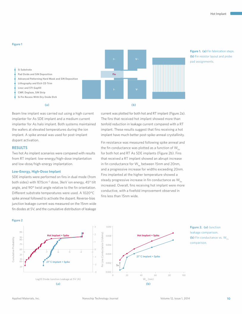
RESULTSTwo hot As implant scenarios were compared with results
from RT implant: low-energy/high-dose implantation
and low-dose/high-energy implantation.
Low-Energy, High-Dose Implant
SDE implants were performed on fins in dual mode (from
both sides) with 1E15cm−2 dose, 3keV ion energy, 45° tilt
angle, and 90° twist angle relative to the fin orientation.
Different substrate temperatures were used. A 1020°C
spike anneal followed to activate the dopant. Reverse-bias
junction leakage current was measured on the 15nm wide
fin diodes at 5V, and the cumulative distribution of leakage
current was plotted for both hot and RT implant (Figure 2a).
The fins that received hot implant showed more than
tenfold reduction in leakage current compared with a RT
implant. These results suggest that fins receiving a hot
implant have much better post-spike-anneal crystallinity.
Fin resistance was measured following spike anneal and
the fin conductance was plotted as a function of Wfin
for both hot and RT As SDE implants (Figure 2b). Fins
that received a RT implant showed an abrupt increase
in fin conductance for Wfin
between 15nm and 20nm,
and a progressive increase for widths exceeding 20nm.
Fins implanted at the higher temperature showed a
steady progressive increase in fin conductance as Wfin
increased. Overall, fins receiving hot implant were more
conductive, with a fivefold improvement observed in
fins less than 15nm wide.
Figure 1. (a) Fin fabrication steps.
(b) Fin resistor layout and probe
pad assignments.
Figure 2. (a) Junction
leakage comparison.
(b) Fin conductance vs. Wfin
comparison.
Figure 1
(b)(a)
Si Substrate
Pad Oxide and SiN Deposition
Advanced Patterning Hard Mask and SiN Deposition
Lithography and Etch CD Trim
Liner and STI Gapfill
CMP, Deglaze, SiN Strip
Si Fin Recess With Dry Oxide Etch
I+ V+
I-
Fin
V-
Figure 2
(b)(a)
Cum
ulat
ive
Prob
abili
ty
Log10 Diode Junction Leakage at 5V (A)
.01
.05.10
.25
.50
.75
.90.95
.99
-3
-2
-1
0
1
3
2
Fin
Line
Con
duct
ance
(1/
ohm
s)
Wfin
(nm)
0 20 40 60 80 100
0.000
0.010
0.008
0.006
0.004
0.002
Hot Implant + Spike
27˚C Implant + Spike
Hot Implant + Spike
27˚C Implant + Spike
-9 -8 -7 -6 -5 -4 -3
5x

11 Volume 12, Issue 1, 2014 Nanochip Technology Journal Applied Materials, Inc.
Hot Implant
To investigate the abrupt change in fin conductance in narrow fins for RT implants, fin crystallinity was analyzed by cross-sectional transmission electron microscopy (XTEM). The crystalline Si (c-Si) is the dark region in the XTEM, while the amorphous Si is the homogeneous light gray layer. An RT-implanted fin of 12nm CD was completely amorphous while a 32nm CD fin exhibited an amorphous outer layer approximately 7nm thick (Figure 3). These results indicate that a narrow fin would be completely amorphous if its width were less than twice the thickness of the amorphous layer (ta), but would have a c-Si core were its width to exceed 2ta.
To investigate the effect of the spike activation anneal on fin crystallinity, XTEM analysis was carried out on a narrow fin and a wide fin following RT As SDE implant and again after spike anneal (Figure 4.) The narrow (6nm) fin had <111> stacking faults near the bottom and was polycrystalline in the top portion, while the 24nm-wide fin was single-crystalline with defects at the top corner. The narrow fin would have been fully amorphous as implanted since its width was less than 2ta, and the wide fin should have had an approximately 10nm c-Si core before the activation anneal. The crystalline core inside the fin plays an important role in recrystallization.
The poor crystallinity of recrystallized fins can be explained by the geometry difference between a planar surface and a fin. In traditional planar devices, the layer amorphized by the SDE implant is planar with its amorphous/crystalline interface parallel to the surface, and recrystallization proceeds by the motion of the interface towards the surface. The recrystallization process is called solid phase epitaxial regrowth (SPER), which occurs at ~550°C and incorporates dopant atoms into the crystal lattice to become electrically active.
The recrystallization of a fin is more complicated than
that of a planar device due to its 3D nature and surface
proximity. A fully amorphized fin has a top surface and
two sidewall surfaces, with the c-Si seed at the bottom
of the fin. It has been reported that an amorphous Si
atom must complete at least two undistorted bonds
to attain SPER.[5-7] This is not a problem for the <100>
surface, but for each atom to form two undistorted
bonds, a two-atom cluster is needed at the <110>
surface and a three-atom cluster at the <111> surface.
This leads to the phenomenon that crystallization
occurs most rapidly in the <100> direction, followed
by <110> and, lastly, <111>.[6-8]
It was also reported that micro-twins can form easily
on the <111> plane.[6] These results agree with those in
Figure 4a, which shows the c-Si after regrowth bounded
by <111> stacking faults. The regrowth proceeded only
for approximately 5nm from the bottom of the fin. The
difficulty in forming two undistorted bonds caused by
the Si/native oxide interface at the vertical fin sidewall
significantly retarded the SPER. In the absence of SPER,
the top portion of the fin in Figure 4a was polycrystalline,
seeded from random nucleation in the amorphous Si
during the 1020°C spike anneal.
Recrystallization on a wide fin is much easier if there
is a c-Si core within the fin. The SPER front propagates
from the c-Si core towards the surface as in the case
of planar SPER. The fin body can be largely defect-free
after recrystallization. However, defects can occur at the
corner of the fin due to the proximity of two orthogonal
surfaces at the top and the sidewall (Figure 4b).
The abrupt increase in fin conductance at 15nm to
20nm Wfin
can be explained by the TEM observation.
The low conductance of Wfin
of 15nm and below resulted
Figure 3. (a) Narrow fin
completely amorphized after
RT implant.
(b) Outer amorphization layer
on wide fin after RT implant.
Figure 4. After spike anneal,
(a) narrow fin was polycrystalline
and (b) wide fin was single-
crystalline with top-corner
defect.
Figure 3
Applied Materials internal data
(b)(a)
20nm 20nm
Figure 4
Applied Materials internal data
(b)(a)
20nm 20nm

12Volume 12, Issue 1, 2014Nanochip Technology JournalApplied Materials, Inc.
Hot Implant
from the full amorphization of the fin during the RT As+
implant and its highly defective state after the spike
anneal. For Wfin
20nm and above a crystalline core inside
the fin promoted SPER that resulted in much improved
crystallinity and therefore much better conductance.
The poor recrystallization after RT implant can be
prevented by introducing hot implant for which the
substrate is held at an elevated temperature. A 6nm fin
remained single-crystalline after hot implant and after
spike anneal (Figure 5).
The improvement in fin crystallinity from hot implant
is explained by the balance of damage generation and
dynamic annealing. The energetic ions damage the Si
lattice during the implantation process. This damage
ranges from isolated point defects, point defect clusters,
and amorphous pockets to continuous amorphous layers.
The SDE implant at RT would amorphize the Si fin.
Amorphization is the result of a competition between
defect accumulation from energetic ion cascades and
defect annihilation and out-diffusion from the damaged
region.
For a given ion mass and temperature, a threshold
dose is required to produce a continuous amorphous
layer in single c-Si. The threshold implant dose for
the amorphization transition is a function of ion mass,
implant temperature, and dose rate.[5,9] Ion implant
produces interstitial-vacancy pairs, the recombination
of which is temperature dependent. Rising temperature
during implantation makes point defects more mobile
and enhances the dynamic annealing and eradication
of these defects, which in turn increases the threshold
dose for the onset of amorphization.[2,4] In this way, hot
As+ SDE implant prevents amorphization of the fins,
which improves their crystallinity, leading to reduced
junction leakage and parasitic resistance.
A hot implant also changes the amount of de-channeling
and defect formation. Substrate amorphization is
prevented, which results in a deeper dopant profile.
Hence the implant energy may need to be reduced to
match the RT implant profile.
High-Energy, Low-Dose Implant
A high-energy, low-dose As RT implant was performed
on the fins at 5E13cm−2 dose, 45keV energy, 20° tilt
angle, and 90° twist angle relative to fin orientation.
Amorphous pockets were seen on a narrow (8nm)
fin (Figure 6a). The 1020°C spike anneal did not fully
recover the fin crystallinity, and a defective region was
seen at the bottom of the implanted region (Figure 6b).
Hot implant was carried out on 8nm fins at the same
implant dose, energy, and tilt angle. The fins were
single-crystalline following hot implant (Figure 6c)
and after spike anneal (Figure 6d), demonstrating hot
implant’s effectiveness in preventing defect formation.
Figure 5. Hot SDE implant
enabled single-crystalline 6nm fin
(a) following implant and
(b) after spike anneal.
Figure 6. 8nm-wide fin after
high-energy, low-dose RT implant.
(a) As implanted and
(b) after spike anneal. Similar
fin after hot implant.
(c) As implanted and
(d) after spike anneal.
Figure 5
Applied Materials internal data
(b)(a)
6nm
20nm
Figure 6
Applied Materials internal data
(d)(c)
(b)(a)
20nm 20nm
20nm 20nm

13 Volume 12, Issue 1, 2014 Nanochip Technology Journal Applied Materials, Inc.
Hot Implant
CONCLUSIONAs+ SDE implants on fins at different substrate temperatures were characterized by resistance and junction leakage measurements, and by TEM analysis. A narrow fin was completely amorphized by the RT implant, and the crystallinity could not be restored during spike anneal as the Si single crystal seed was at the bottom of the fin and the SPER was severely retarded by fin sidewall surface proximity. A wide fin retained an inner crystalline core following RT SDE implant, which served as seed for recrystallization during spike anneal. Hot implant prevented amorphization of narrow fins during SDE implant by raising the substrate temperature and thereby increasing the threshold dose for amorphization. A 6nm-wide vertical fin remained single-crystalline after hot As+ SDE implant and after spike anneal. The hot implant improved narrow fin conductance fivefold and junction leakage more than tenfold.
Halo implants were also characterized on narrow fins. RT As+ halo implant produced amorphous pockets; a defective region remained after spike anneal. Narrow fins remained single-crystalline following both implant and anneal when hot As+ halo implant was used. Thus, hot implant has demonstrated effectiveness in controlling implant damage and optimizing the doping level in very narrow CD FinFET structures.
ACKNOWLEDGEMENTSThe authors acknowledge the staff of the Applied Materials Maydan Technology Center for fabricating the device structures; D. Yang, K. Lie, and the Dielectric Systems and Modules business unit at Applied Materials for fin recess processing; and S. Moffatt and F. Sinclair for helpful discussions.
REFERENCES[1] C. Auth, et al., “A 22nm High Performance and Low-Power
CMOS Technology Featuring Fully-Depleted Tri-Gate Transistors, Self-Aligned Contacts and High Density MIM Capacitors,” VLSI Tech. Symp. Dig., p. 131, 2012.
[2] R. Duffy, et al., “Solid Phase Epitaxy Versus Random Nucleation and Growth in Sub-20nm Wide Fin Field-Effect Transistors,” Appl. Phys. Lett., 90, 241912, 2007.
[3] M. Togo, et al., “Heated Implantation with Amorphous
Carbon CMOS Mask for Scaled FinFETs,” VLSI Tech.
Symp. Dig., p. 196, 2013.
[4] L. Pelaz, et al., “Ion-Beam-Induced Amorphization and Recrystallization in Silicon,” J. Appl. Phys., 96, 5947, 2004.
[5] Y. Kunii, et al., “Amorphous-Si/Crystalline-Si Facet
Formation During Si Solid-Phase Epitaxy Near Si/SiO2
Boundary,” J. Appl. Phys., 56, 279, 1984.
[6] R. Drosd and J. Washburn, “Some Observations on
the Amorphous to Crystalline Transformation in
Silicon,” J. Appl. Phys., 53, 397, 1982.
[7] L. Csepregi, et al., “Regrowth Behavior of Ion-Implanted
Amorphous Layers on <111> Silicon,” Appl. Phys. Lett.,
29, 92, 1976.
[8] J. Brice and P. Wiffin, “The Temperature Distribution
in Pulled Germanium Crystals During Growth,”
Solid-State Electron., 7, 183, 1964.
[9] F. Morehead, et al., “Formation of Amorphous Silicon
by Ion Bombardment as a Function of Ion, Temperature,
and Dose,” J. Appl. Phys., 43, 1112, 1972.
AUTHORS Bingxi Wood is a senior technology program manager
in the Advanced Product and Technology Development
group of the Silicon Systems Group at Applied Materials.
She holds her Ph.D. in physics from Rensselaer
Polytechnic Institute.
Fareen Adeni Khaja is a member of technical staff in the
Varian Semiconductor Equipment business unit of the
Silicon Systems Group at Applied Materials. She earned
her M.S. in electrical engineering from North Carolina
State University.
Naushad Variam is a senior director of strategic marketing
in the Varian Semiconductor Equipment business unit
of the Silicon Systems Group at Applied Materials. He
received his Ph.D. in chemical engineering from the
University of Washington.
Adam Brand is the director of transistor technology in
the Advanced Product and Technology Development
group of the Silicon Systems Group at Applied Materials.
He holds his M.S. in electrical engineering from the
Massachusetts Institute of Technology.
ARTICLE CONTACT [email protected]
PROCESS SYSTEMS USED IN STUDY Applied Varian VIISta® 900XPT Medium Current Implant
Applied Varian VIISta® Trident High Current Implant

14Volume 12, Issue 1, 2014Nanochip Technology JournalApplied Materials, Inc.
Plasma Doping of High Aspect Ratio Structures
KEYWORDS
3D NAND
CMOS Image Sensor
Deep Trench Isolation
Ion Implantation
Plasma Doping
Secondary Ion Mass Spectroscopy (SIMS)
As semiconductor device technology rapidly transitions to
3D structures, doping specific regions of these devices to
enable reliable electrical characteristics presents a unique
high-value problem. Doping high aspect ratio (HAR)
structures uniformly and with reliable repeatability poses
a major challenge for device manufacturers, particularly in
the advanced memory and CMOS image sensor technology
spaces. Plasma doping offers an effective solution that will
aid in commercializing these emerging architectures.
CMOS technology scaling limitations have led to the
emergence of vertically integrated cells, which leading-
edge chipmakers are already introducing into mass
production.[1] These low-power, high-performance devices
are likely to be more widely adopted as they facilitate
scaling and become less costly.[2,3] In the case of NAND
flash memory, chip manufacturers are aggressively
pursuing various approaches to 3D fabrication and
some are already in pilot production. Many challenges
are associated with these new devices, including new
transistor architecture, storage mechanisms, and gate
fabrication. Each case involves HAR structures that may
require doping to improve or even enable device operation.
Meanwhile, scaling is driving CMOS image sensor device
challenges in pixel-to-pixel isolation, dark-current
reduction, and noise reduction.[4-6] This article reports
the inherent advantages of plasma doping as an enabling
technology for optimizing doping in these challenging
HAR structures.
SAMPLE PREPARATIONTo evaluate plasma doping performance, HAR Si trench
structures were fabricated and then doped using
PH3-based or BF
3 plasma. Next, they were subjected to
a post-implant process flow designed to mimic a typical
PR or mask removal. Wet chemistry (SPM/SC1) was
used and activation anneal performed prior to analysis.
Transmission electron microscopy (TEM) was used
to verify the surface response and poly-Si gap fill to
examine voiding between trenches (Figure 1a).
Completed structures (Figure 1b) were analyzed using a
SIMS technique that averages the dopant concentration
over several features as the SIMS spot size is larger
than the features of interest.
Figure 1. Test structure.
(a) Preparation process flow.
(b) Completed HAR trench.
Figure 1
(b)(a)
Applied Materials internal data
50nm
h=27
4nm
AR~8:1
w=36nm
w=29nm
Fill With Poly-SiPlasma Treatment Initial Structure

15 Volume 12, Issue 1, 2014 Nanochip Technology Journal Applied Materials, Inc.
Plasma Doping
RESULTS AND ANALYSISStudy results showed promise in current memory and
CMOS image sensor applications. They also indicate
the potential for proliferating plasma doping to
anticipated future applications.
Memory
As NAND flash memory technology scales, 2D memory
will reach fundamental physical limitations as it
approaches the 10nm node, giving rise to several
new challenges.[7,8] In particular, the floating gate 2D
NAND cell will transition to a 3D NAND in which the
cells are stacked vertically. Effectively doping the cell
sidewall of the resulting HAR channel is one of the
major challenges this change poses.
The stacked memory cells may number 24, 32, or more
as the technology scales (Figure 2a). The channel
region must not only be doped at a precisely controlled
concentration; it must be uniformly doped along the
entire length of the channel to avoid threshold voltage
variation across the device.
Figure 2
(a)
Channel
Figures 2b and 2c depict uniform doping along the HAR
trench with doping concentration on the order of e18
to e19 as a function of the requested dose. The higher
dopant concentration at the bottom results from the
unobstructed line of sight that facilitates both ions and
neutrals reaching the bottom of the trench. These data
also demonstrate the potential benefit of plasma doping
for HAR staircase contacts in which a high, shallow
concentration of dopant ions may be required to improve
contact resistance.
The flexibility to tune the sidewall doping concentration
as a function of various input parameters is a key
feature of the plasma doping approach. Alternatives,
such as traditional ion implant, will be limited by the
dimensionality of a HAR structure and in-situ doping,
using low-pressure CVD for example, may be limited by
the required dopant concentration and placement of the
dopant species into the substrate at a specified depth.
In addition, plasma doping of the channel employs
low implant bias and can operate at different plasma
densities to tune the deposition and residual damage
responses.
CMOS Image Sensors
With the continued growth of the CMOS image sensor
market, the demand for better resolution and pixel growth
continues to push the image sensor manufacturers. A
critical challenge affecting this segment is the requirement
to reduce dark current while scaling image sensor
technology. As shown in Figure 3, plasma doping is one
approach to reducing dark current.[4,6]
Figure 2. 3D memory cell
structure doping.
(a) HAR channel doping region.
(b) HAR SIMS data with
dose sensitivity and
(c) HAR SIMS data with
energy sensitivity.
(b)
Con
cent
rati
on (
a/cc
)
Depth (nm)
200 600550450 500400350250 300
1.0E+17
1.0E+18
1.0E+19
1.0E+20
1.0E+21
1.0E+22 3kV, 3e153kV, 1e16
(c)
Con
cent
rati
on (
a/cc
)
Depth (nm)
200 600550450 500400350250 300
1.0E+17
1.0E+18
1.0E+19
1.0E+20
1.0E+21
1.0E+22 1kV, 3e153kV, 3e15
Applied Materials internal data
16Volume 12, Issue 1, 2014Nanochip Technology JournalApplied Materials, Inc.
Plasma Doping
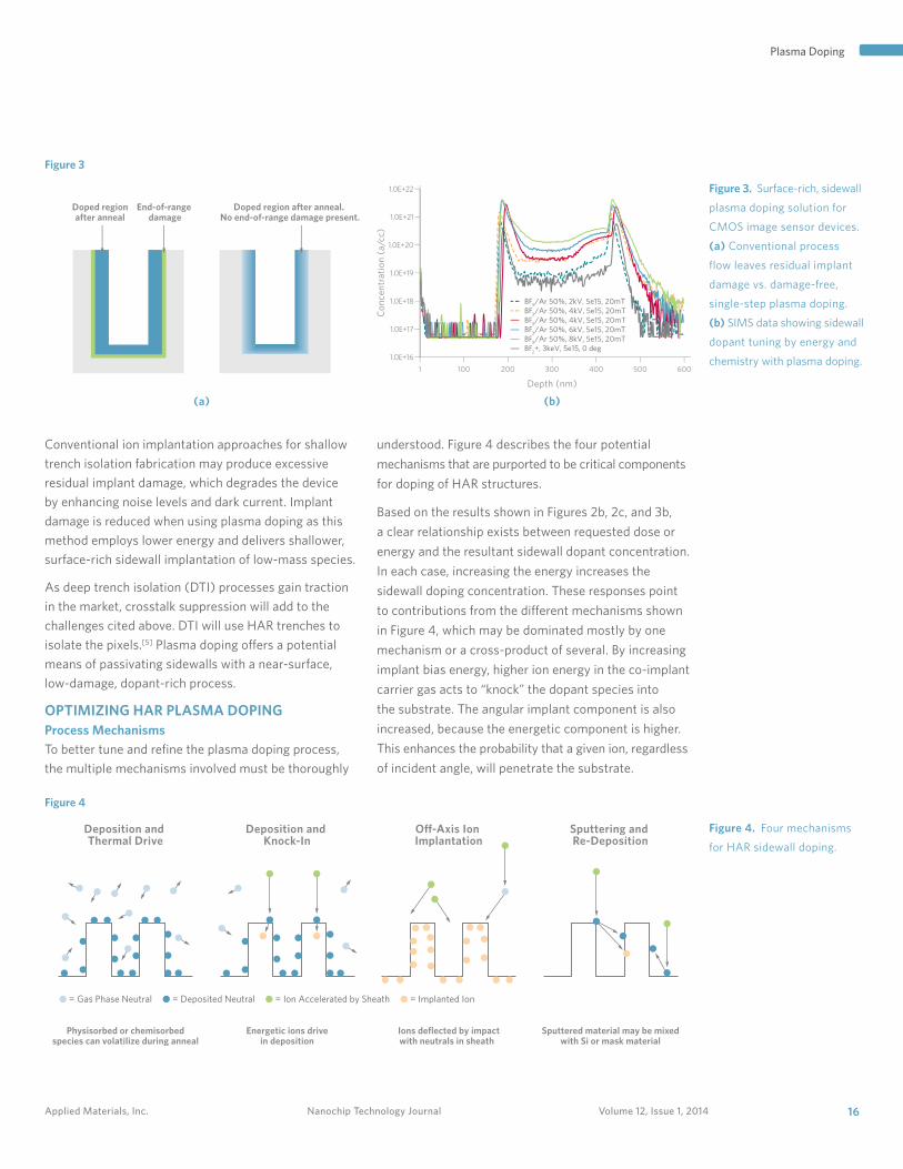
Conventional ion implantation approaches for shallow
trench isolation fabrication may produce excessive
residual implant damage, which degrades the device
by enhancing noise levels and dark current. Implant
damage is reduced when using plasma doping as this
method employs lower energy and delivers shallower,
surface-rich sidewall implantation of low-mass species.
As deep trench isolation (DTI) processes gain traction
in the market, crosstalk suppression will add to the
challenges cited above. DTI will use HAR trenches to
isolate the pixels.[5] Plasma doping offers a potential
means of passivating sidewalls with a near-surface,
low-damage, dopant-rich process.
OPTIMIZING HAR PLASMA DOPING Process Mechanisms
To better tune and refine the plasma doping process,
the multiple mechanisms involved must be thoroughly
understood. Figure 4 describes the four potential
mechanisms that are purported to be critical components
for doping of HAR structures.
Based on the results shown in Figures 2b, 2c, and 3b,
a clear relationship exists between requested dose or
energy and the resultant sidewall dopant concentration.
In each case, increasing the energy increases the
sidewall doping concentration. These responses point
to contributions from the different mechanisms shown
in Figure 4, which may be dominated mostly by one
mechanism or a cross-product of several. By increasing
implant bias energy, higher ion energy in the co-implant
carrier gas acts to “knock” the dopant species into
the substrate. The angular implant component is also
increased, because the energetic component is higher.
This enhances the probability that a given ion, regardless
of incident angle, will penetrate the substrate.
Figure 3. Surface-rich, sidewall
plasma doping solution for
CMOS image sensor devices.
(a) Conventional process
flow leaves residual implant
damage vs. damage-free,
single-step plasma doping.
(b) SIMS data showing sidewall
dopant tuning by energy and
chemistry with plasma doping.
Figure 4. Four mechanisms
for HAR sidewall doping.
Figure 3
(a) (b)
Con
cent
rati
on (
a/cc
)Depth (nm)
1 600500400300100 200
1.0E+16
1.0E+17
1.0E+18
1.0E+19
1.0E+20
1.0E+21
1.0E+22
BF3/Ar 50%, 2kV, 5e15, 20mT
BF3/Ar 50%, 4kV, 5e15, 20mT
BF3/Ar 50%, 4kV, 5e15, 20mT
BF3/Ar 50%, 6kV, 5e15, 20mT
BF3/Ar 50%, 8kV, 5e15, 20mT
BF2+, 3keV, 5e15, 0 deg
Doped region after anneal. No end-of-range damage present.
Doped regionafter anneal
End-of-range damage
Figure 4
Deposition and Thermal Drive
Physisorbed or chemisorbedspecies can volatilize during anneal
Energetic ions drivein deposition
Ions deflected by impactwith neutrals in sheath
Sputtered material may be mixedwith Si or mask material
Deposition and Knock-In
O�-Axis Ion Implantation
Sputtering and Re-Deposition
= Gas Phase Neutral = Deposited Neutral = Ion Accelerated by Sheath = Implanted Ion
17 Volume 12, Issue 1, 2014 Nanochip Technology Journal Applied Materials, Inc.
Plasma Doping
The deposition and thermal drive mechanism is
enhanced when plasma doping is followed directly by
anneal without an intervening cleaning step. In this
case, dopant remains on or near the surface and acts as
a source during the subsequent processing steps. The
dopant concentration in the sidewall may be enhanced
by the in-diffusion of dopant deposition from the
surface into the substrate. Such an approach is possible
when a hard mask (oxide/nitride) is used, but is not
compatible with a PR strip process.
In addition to the data shown in this article, which can
be supported by the mechanisms cited above, attempts
to model the plasma doping behavior are underway that
will advance understanding of these mechanisms and
make possible further optimization of these processes.
System Innovations
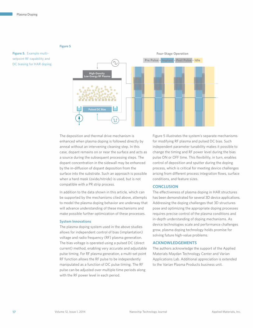
The plasma doping system used in the above studies
allows for independent control of bias (implantation)
voltage and radio frequency (RF) plasma generation.
The bias voltage is operated using a pulsed DC (direct
current) method, enabling very accurate and adjustable
pulse timing. For RF plasma generation, a multi-set point
RF function allows the RF pulse to be independently
manipulated as a function of DC pulse timing. The RF
pulse can be adjusted over multiple time periods along
with the RF power level in each period.
Figure 5 illustrates the system’s separate mechanisms
for modifying RF plasma and pulsed DC bias. Such
independent parameter tunability makes it possible to
change the timing and RF power level during the bias
pulse ON or OFF time. This flexibility, in turn, enables
control of deposition and sputter during the doping
process, which is critical for meeting device challenges
arising from different process integration flows, surface
conditions, and feature sizes.
CONCLUSIONThe effectiveness of plasma doping in HAR structures
has been demonstrated for several 3D device applications.
Addressing the doping challenges that 3D structures
pose and optimizing the appropriate doping processes
requires precise control of the plasma conditions and
in-depth understanding of doping mechanisms. As
device technologies scale and performance challenges
grow, plasma doping technology holds promise for
solving future high-value problems.
ACKNOWLEDGEMENTSThe authors acknowledge the support of the Applied
Materials Maydan Technology Center and Varian
Applications Lab. Additional appreciation is extended
to the Varian Plasma Products business unit.
Figure 5
Pulsed DC Bias
Four-Stage Operation
Pre Pulse – Implant – Post Pulse – Idle
High-Density Low-Energy RF Plasma
Figure 5. Example multi-
setpoint RF capability and
DC biasing for HAR doping.

18Volume 12, Issue 1, 2014Nanochip Technology JournalApplied Materials, Inc.
Plasma Doping
REFERENCES[1] Samsung Village, “Samsung Starts Mass Producing
Industry’s First 3D Vertical NAND Flash,”
http://www.samsungvillage.com/blog/2013/08/
sansungblog-samsung-starts-mass-producing-
industrys-first-3d-vertical-nand-flash-.html;
August, 2013.
[2] K. Ahmed and K. Schuegraf, “Transistor Wars—Rival
Architectures Face Off in a Bid to Keep Moore's Law
Alive,” IEEE Spectrum, No.11, 2011.
[3] K. Kuhn, “CMOS Scaling for the 22nm Node and
Beyond: Device Physics and Technology,” IEDM, 2011.
[4] C-R Moon, et al., “Application of Plasma-Doping
(PLAD) Technique to Reduce Dark Current of CMOS
Image Sensors,” IEEE Electron Device Lett., Vol. 28,
No. 2, Feb. 2007.
[5] Y. Kitamura, et al., “Suppression of Crosstalk by
Using Backside Deep Trench Isolation for 1.12μm
Backside Illuminated CMOS Image Sensor,” IEDM
2012-537.
[6] S.G. Pyo, et al., “Effect of B2H
6 Plasma Doping on
the Shallow Trench Isolation in CMOS Image Sensor
Device,” IEEE Electron Device Lett., Vol. 33, No. 11,
Nov. 2012.
[7] D. Sekar, “The Flash Industry's Direction, and
MonolithIC 3D Inc.'s Solution,”
http://www.monolithic3d.com/2/post/2011/12/
where-is-the-nand-flash-industry-heading-and-
monolithic-3d-incs-solution.html.
[8] C. Demerjian, “Applied Materials Talks About 3D
NAND Flash Production,” SemiAccurate, July 2013.
AUTHORSDeven Raj is a member of technical staff in the Varian
Semiconductor Equipment business unit of the Silicon
Systems Group at Applied Materials. He holds his B.S.
in chemical engineering from the Georgia Institute of
Technology.
Jun S. Lee is a member of technical staff in the Varian
Semiconductor Equipment business unit of the Silicon
Systems Group at Applied Materials. He earned his
D. Eng. from the University of Massachusetts Lowell.
Helen Maynard is a senior marketing manager in the
Varian Semiconductor Equipment business unit of
the Silicon Systems Group at Applied Materials.
She received her Ph.D. in materials science from the
University of Wisconsin–Madison.
ARTICLE [email protected]
PROCESS SYSTEM USED IN STUDYApplied Varian VIISta® PLAD Ultra High Dose Implant

19 Volume 12, Issue 1, 2014 Nanochip Technology Journal Applied Materials, Inc.
As planar CMOS device scaling continues, optimizing
ultra-shallow junction (USJ) dopant activation and leakage is
increasingly challenging. Integrating anneal technologies
can mitigate the difficulty. Boosting dopant activation while
preserving junction profile and depth is a fine balance strongly
influenced by stabilization temperature. The low stabilization
temperature of laser millisecond (msec) anneal prevents
formation of dopant-deactivating interstitials, preserves
junction depth, enhances activation by the following spike
anneal, and leads to higher transistor drive current.
Junction optimization is one of the key challenges in
producing advanced CMOS devices as it is essential to
minimize the parasitic resistance of the device and fully
realize the drive current available from advanced transistors.
Device scaling requires abrupt USJ with high dopant
activation while maintaining low junction leakage. Msec
anneal was initially introduced as a means of boosting
dopant activation with minimal diffusion.[1,2] Spike annealing
is the hallmark of shallow junction engineering, because
of its ability to both activate dopants and control diffusion.
However, no consensus has been reached on integrating
msec anneal with spike anneal.[1, 3-5] This article explores
the effects of anneal sequences (msec anneal followed
by spike anneal and vice versa) and demonstrates that
stabilization temperature of the msec anneal plays a
significant role in dopant activation.
EXPERIMENTAL STUDIESStabilization Temperature
During the msec anneal, temperature stabilization (which
is essentially the wafer pre-heat performed as a single-
or multi-step process) is required prior to jumping to the
final high temperature (Figure 1). This stabilization is
critical for improving within-wafer uniformity and avoiding
wafer breakage. The actual stabilization temperature
depends on the anneal system technology and application.
In general, flash-lamp msec systems require higher
stabilization temperatures than laser anneal systems. In
this study, experiments were conducted to determine the
effects of stabilization temperature on dopant activation.
PMOS source/drain extension (SDE) dopants were
implanted (with zero degrees tilt) into blanket n-type
<100> Si wafers at -100°C. The implant sequence
consisted of germanium (12keV, 5E14/cm2) followed by
carbon (3keV, 5E14/cm2) and boron (0.4keV, 1E15/cm2).
Implant conditions were designed with a cryogenic implant
temperature of -100°C, germanium pre-amorphization
implant, and carbon co-implant to capitalize on the
KEYWORDS
Activation
Anneal
Dopant
Laser
Millisecond
Msec
Spike
Ultra-Shallow Junction
Integrating Millisecond and Spike Anneals to Optimize Dopant Activation
Figure 1. Wafer temperature
profile of msec anneal.
Figure 1
Tem
pera
ture
Time
Preheat Temperature
JumpTemperature
Dwell Time

20Volume 12, Issue 1, 2014Nanochip Technology JournalApplied Materials, Inc.
Integrated Anneals
physics of implant damage engineering for boron dopant
activation and profile control in the USJ. Spike anneals
with peak temperatures ranging from 700°C to 950°C
were applied to simulate various stabilization temperatures.
Post-anneal sheet resistance (Rs) was measured by a
high-resolution, four-point Capres microprobe. Secondary
ion mass spectroscopy (SIMS) data were analyzed to
evaluate the junction profile and dopant activation.
As shown in Figure 2, Rs data at different spike
temperatures are normalized by the 700°C condition.
Rs increases as spike temperature rises, and reaches a
maximum at 850°C, which is consistent with previous
studies.[6] The rise in Rs is attributed to dopant deactivation.
Si interstitials are created during implants[6] and can
diffuse back to the implanted region and form boron-
interstitial clusters (BICs) during post-implant anneals.
BIC formation, which depends on the anneal temperature,
makes the boron dopants electrically inactive. Intermediate
temperatures (800-900˚C) show the highest Rs linked
to high BIC formation and thus should be avoided at the
stabilization step during the msec anneal to maximize
dopant activation. Once BICs are formed, a much higher
thermal budget is required to recover dopant activation
by dissolving them. But higher thermal budgets produce
deeper junctions by increasing diffusion rates. Therefore,
a low stabilization temperature is essential for achieving
high dopant activation while maintaining the USJ profile.
Anneal Sequence
In this study alternating flow sequences were explored
between spike and msec anneals to identify ideal
conditions for junction annealing. PMOS SDE cryogenic
implants were applied under the same conditions as
described above.
Figure 2
Nor
mal
ized
Rs
Spike Temperature (˚C)
700 750 800 850 900 950
0.8
1.1
0.9
1.2
1.0
Figure 3a plots the Rs data of various anneal conditions,
normalized by the msec 1200°C condition, while Figure 3b
plots SIMS results of corresponding anneal conditions.
Junction depth (Xj) is taken at 5E18cm-3, and the normalized
1/(median Rs*Xj) is plotted in Figure 4, which reflects
dopant electrical activation.
Of all the anneal conditions, msec 1200°C has the lowest
Rs, while spike 750°C has the highest—approximately
70% higher than that of msec 1200°C, which cannot
be explained by the subtle difference in Xj. Meanwhile,
the anneal sequence results in clear differences. Rs is
approximately 50% lower after the msec + spike sequence
despite the shallower junction of this sequence. This Rs
difference is related to dopant activation.
Figure 3
(b)(a)
Nor
mal
ized
Rs
Msec 1200°C Msec 1200°C+ Spike 750°C
Spike 750°C +Msec 1200°C
Spike 750°C0
0.5
1.0
2.0
1.5
Bor
on C
once
ntra
tion
(cm
-3)
Depth (nm)
0 5 10 2015
1E+16
1E+17
1E+18
1E+19
1E+20
1E+21
1E+22 Msec 1200°CSpike 750°CMsec 1200°C + Spike 750°CSpike 750°C + Msec 1200°C
Figure 2. Normalized Rs at
various anneal temperatures.
Figure 3. Comparison
of anneal conditions.
(a) Normalized Rs data and
(b) SIMS data.

21 Volume 12, Issue 1, 2014 Nanochip Technology Journal Applied Materials, Inc.
Integrated Anneals
In the spike and spike + msec cases, BICs are formed at
the intermediate spike temperature, adversely affecting
dopant activation. Subsequent 1200°C msec anneal can
improve Rs only to some extent, at the cost of a deeper
junction. Complete dissolution of BICs requires even higher
thermal budget, which inevitably leads to a deeper junction.
On the other hand, in the msec and msec + spike scenarios,
the msec stabilization temperature is only 400°C, which
is low enough to prevent Si interstitials from diffusing.
The fast msec anneal temperature ramp-up and high
peak temperature are able to annihilate the Si interstitials
before they form clusters, avoiding dopant deactivation
from occurring in the first place. Although msec anneal
is effective in dissolving Si interstitials, a subsequent spike
anneal is still recommended to repair residual implant
damage. Clearly, a low stabilization temperature affords
substantial dopant activation benefits.
Experiments with spike temperatures of 800°C and 900°C
were also performed and the same trends were observed.
Validation of Results
The anneal sequence effects were validated on device
wafers. Gate-first transistors were fabricated, with
the shortest gate length being approximately 50nm.
Source/drain (S/D) activation annealing was performed
on splits. Figure 5 compares the Idsat
–Ioff
curve for the
split subjected to conventional spike 1050°C anneal vs.
the split processed with a msec 1200°C followed by
spike 1050°C. Clearly, at the same Ioff
(100nA/µm), the
Idsat
of the msec + spike split is more than 10% higher.
In addition, Miller capacitors were fabricated to characterize
the S/D dopant lateral out-diffusion under various anneal
conditions. Figure 6 shows the derived Lov (gate-S/D
overlap length) for both spike 1050°C and msec 1200°C
+ spike 1050°C splits. Essentially, both anneal conditions
lead to the same Lov, implying that the addition of
msec anneal does not cause additional dopant lateral
out-diffusion. Thus, the gain in Idsat
can be attributed
to superior S/D dopant activation, rather than to the
shorter electrical gate length.
Figure 4
Nor
mal
ized
1/(
Med
ian
Rs *
Xj)
Msec 1200°C Msec 1200°C+ Spike 750°C
Spike 750°C +Msec 1200°C
Spike 750°C0
0.8
1.0
0.4
0.2
1.2
0.6
Figure 5
LogI
o� (
A/μ
m)
Idsat
(mA/μm)
0.2 0.4 0.6 1.0 1.20.8-10
-4
-6
-8
-2 Spike 1050°CMsec 1200°C + Spike 1050°C
Figure 6
Prob
abili
ty P
erce
ntag
e
Lov (nm)
Spike 1050°CMsec 1200°C + Spike 1050°C
26 28 30 32 34
Figure 4. Normalized
1/(Median Rs*Xj) of
corresponding splits.
Figure 5. Msec + spike
anneal sequence boosts
transistor Idsat
over that from
spike anneal only.
Figure 6. Lov derived
through Miller capacitors
matches closely for spike
and msec + spike anneals.
22Volume 12, Issue 1, 2014Nanochip Technology JournalApplied Materials, Inc.
Integrated Anneals
CONCLUSIONA low msec stabilization temperature is crucial for
achieving high dopant activation while preserving an
abrupt dopant profile and USJ depth. The msec + spike
scheme also exhibits significantly higher dopant activation
than the spike alone and spike + msec approach, which
is attributable to the substantial annihilation of BICs.
These results were validated on gate-first transistors,
which exhibited higher Idsat
for the msec + spike sequence
than for the spike-only process.
ACKNOWLEDGEMENTSThe authors acknowledge the contributions to this work
of D. Kouzminov, B. Colombeau, and N. Variam of the Varian
Semiconductor Equipment business unit; S. Muthukrishnan,
A. Mayur, and S. Moffatt of the Front End Products
business unit; A. Brand of the Advanced Product and
Technology Development Group; and the staff of the
Applied Materials Maydan Technology Center.
REFERENCES[1] J-P Lu, et al., “Millisecond Anneal for Ultra-Shallow
Junction Applications,” Ext. Abs. of 10th Intl.
Workshop on Junction Tech., 2010.
[2] T. Sanuki, et al., “High-Performance 45nm node CMOS
Transistors Featuring Flash Lamp Annealing (FLA),”
Intl. Electron Devices Meeting, IEEE, p. 281, 2007.
[3] T. Hoffmann, et al., “Laser Annealed Junctions:
Process Integration Sequence Optimization for
Advanced CMOS Technologies,” Ext. Abs. of 7th Intl.
Workshop on Junction Tech., p. 137, 2007.
[4] T. Yamamoto, et al., “Advantages of a New Scheme
of Junction Profile Engineering with Laser Spike
Annealing and Its Integration into a 45-nm Node
High Performance CMOS Technology,” Intl. Electron
Devices Meeting, IEEE, 2007.
[5] S. Endo, et al., “Novel Junction Engineering Scheme
Using Combination of LSA and Spike-RTA,” Ext. Abs.
of 7th Intl. Workshop on Junction Tech., p. 135, 2007.
[6] B. Colombeau, et al., “Current Understanding and
Modeling of B Diffusion and Activation Anomalies in
Preamorphized Ultra-Shallow Junctions,” Mat. Res.
Soc. Symp. Proc., Vol. 810, 2004.
AUTHORS Shiyu Sun is a process integration engineer in the
Advanced Product and Technology Development group
of the Silicon Systems Group at Applied Materials. He
holds his Ph.D. in physics from Stanford University.
Shashank Sharma is a member of technical staff in the
Front End Products business unit of the Silicon Systems
Group at Applied Materials. He earned his Ph.D. in
chemical engineering from the University of Louisville.
Kalipatnam “Vivek” Rao is a process applications
manager in the Varian Semiconductor Equipment
business unit of the Silicon Systems Group at Applied
Materials. He received his Ph.D. in materials science
from the University of Arizona and an MBA from
Babson College.
Ben Ng is a member of technical staff in the Front End
Products business unit of the Silicon Systems Group
at Applied Materials.
ARTICLE [email protected]
PROCESS SYSTEMS USED IN STUDY Applied Varian VIISta® Trident PTCII XP High Current Implant
Applied Vantage® Radiance™Plus RTP
Applied Vantage® Astra™ DSA

www.appliedmaterials.com3050 Bowers AvenueP.O. Box 58039Santa Clara, CA 95054-3299U.S.A.Tel: +1-408-727-5555
Applied Materials and the Applied Materials logo are registered trademarks.
All trademarks so designated or otherwise indicated as product names or services
are trademarks of Applied Materials, Inc. in the U.S. and other countries. All other
product and service marks contained herein are trademarks of their respective owners.
© 2014 Applied Materials, Inc. All rights reserved.
Printed in the U.S. 11/13 2K