MUSTAFA ALHAHIM EE497 DR.HOWE Five Bands Equalizer€¦ · MUSTAFA ALHAHIM . EE497 . DR.HOWE ....
12
1 MUSTAFA ALHAHIM EE497 DR.HOWE Mustafa AlHashim, Electrical Engineering Project Advisor: Mitchell, Marc April 26, 2017 Evansville, Indiana Five Bands Equalizer
Transcript of MUSTAFA ALHAHIM EE497 DR.HOWE Five Bands Equalizer€¦ · MUSTAFA ALHAHIM . EE497 . DR.HOWE ....
1
MUSTAFA ALHAHIM
EE497
DR.HOWE
Mustafa AlHashim, Electrical Engineering
Project Advisor: Mitchell, Marc
April 26, 2017
Evansville, Indiana
Five Bands Equalizer
2
Table of Contents
I. Introduction
II. Background
III. Hardware
- Hardware design
- Calculations
- Simulations
- Data
List of Figures
1- Design of Multi-Feedback Band Pass Filter
2- Five bands equalizers circuit
3- Simulations and frequencies respond of 100 Hz band.
4- Simulations and frequencies respond 0f 500 Hz band.
5- Simulations and frequencies respond of 5000 Hz band.
6- Simulations and frequencies respond of 10000 Hz band.
7- Simulations and frequencies respond of 15000 Hz band.
8- Outputs
9- Data
10- Picture of the Final project
11- Picture of the circuits
List of Tables
1- Calculated values.
3
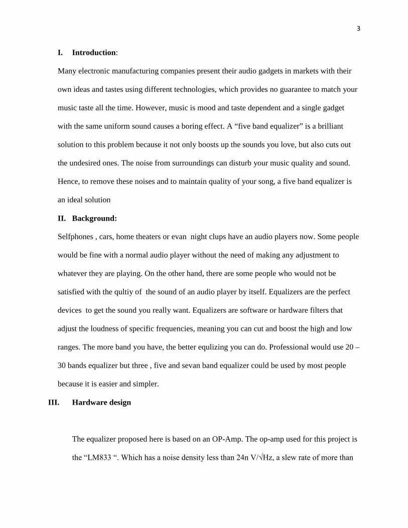
I. Introduction:
Many electronic manufacturing companies present their audio gadgets in markets with their
own ideas and tastes using different technologies, which provides no guarantee to match your
music taste all the time. However, music is mood and taste dependent and a single gadget
with the same uniform sound causes a boring effect. A “five band equalizer” is a brilliant
solution to this problem because it not only boosts up the sounds you love, but also cuts out
the undesired ones. The noise from surroundings can disturb your music quality and sound.
Hence, to remove these noises and to maintain quality of your song, a five band equalizer is
an ideal solution
II. Background:
Selfphones , cars, home theaters or evan night clups have an audio players now. Some people
would be fine with a normal audio player without the need of making any adjustment to
whatever they are playing. On the other hand, there are some people who would not be
satisfied with the qultiy of the sound of an audio player by itself. Equalizers are the perfect
devices to get the sound you really want. Equalizers are software or hardware filters that
adjust the loudness of specific frequencies, meaning you can cut and boost the high and low
ranges. The more band you have, the better equlizing you can do. Professional would use 20 –
30 bands equalizer but three , five and sevan band equalizer could be used by most people
because it is easier and simpler.
III. Hardware design
The equalizer proposed here is based on an OP-Amp. The op-amp used for this project is
the “LM833 “. Which has a noise density less than 24n V/√Hz, a slew rate of more than
4
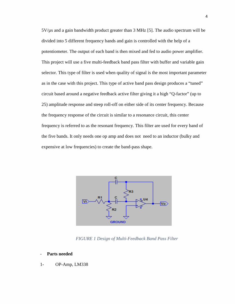
5V/µs and a gain bandwidth product greater than 3 MHz [5]. The audio spectrum will be
divided into 5 different frequency bands and gain is controlled with the help of a
potentiometer. The output of each band is then mixed and fed to audio power amplifier.
This project will use a five multi-feedback band pass filter with buffer and variable gain
selector. This type of filter is used when quality of signal is the most important parameter
as in the case with this project. This type of active band pass design produces a “tuned”
circuit based around a negative feedback active filter giving it a high “Q-factor” (up to
25) amplitude response and steep roll-off on either side of its center frequency. Because
the frequency response of the circuit is similar to a resonance circuit, this center
frequency is referred to as the resonant frequency. This filter are used for every band of
the five bands. It only needs one op amp and does not need to an inductor (bulky and
expensive at low frequencies) to create the band-pass shape.
FIGURE 1 Design of Multi-Feedback Band Pass Filter
- Parts needed
1- OP-Amp, LM338
5
2- Resistors
3- Capacitors
4- Audi jack
5- 12 volt power supply
6- Potentiometers
- Hardware circuit
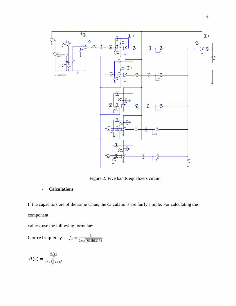
The five bands are located at the center of the circuit. The filter on the left of the
circuit is a buffer. The buffer is non-inverting amplifier circuit that provides a high
input impedance along with all the advantages gained from using an operational
amplifier, with a gain of two[6]. The input signal is divided by the resistive network
comprising R1 and R2. Hence the net gain of this amplifier is unity. The two 100kΩ
resistors (R1 and R2) are used as a voltage divider and the junction voltage is fed to
its positive input through R1. This divider has enough power to feed all other op-
amps directly. The filter on the right is Signal Adder. The output of each band is
mixed at variable gain selector while user choosing gain for each band of frequency,
thus selecting which band of frequency will dominate in output and then fed to an
audio power amplifier. Proper quality factor (Q) needs to be selected to avoid overlap
in adjacent bands as this introduces coloration into the audio signals.
6
Figure 2: Five bands equalizers circuit
- Calculations
If the capacitors are of the same value, the calculations are fairly simple. For calculating the
component
values, use the following formulae:
Centre frequency ∶ 𝑓𝑓0 = 12𝜋𝜋(𝑅𝑅3||𝑅𝑅2)𝑅𝑅1
𝐻𝐻(𝑠𝑠) =𝐺𝐺𝑓𝑓0𝑠𝑠𝑄𝑄
𝑠𝑠2+𝑓𝑓𝑜𝑜𝑄𝑄 𝑠𝑠+𝑓𝑓02
7
Bandwidth ∶ 𝐵𝐵 = 1𝜋𝜋𝜋𝜋𝑅𝑅1
Quality factor ∶ 𝑄𝑄 = 𝑓𝑓0𝐵𝐵
Gain ∶ 𝐴𝐴 = −𝑅𝑅3/2𝑅𝑅1
These can be combined to give the following formulae:
R1 = Q/2πfoAC
R2 = Q/2πfoC (2Q2–A)
R3 = Q/πfoC
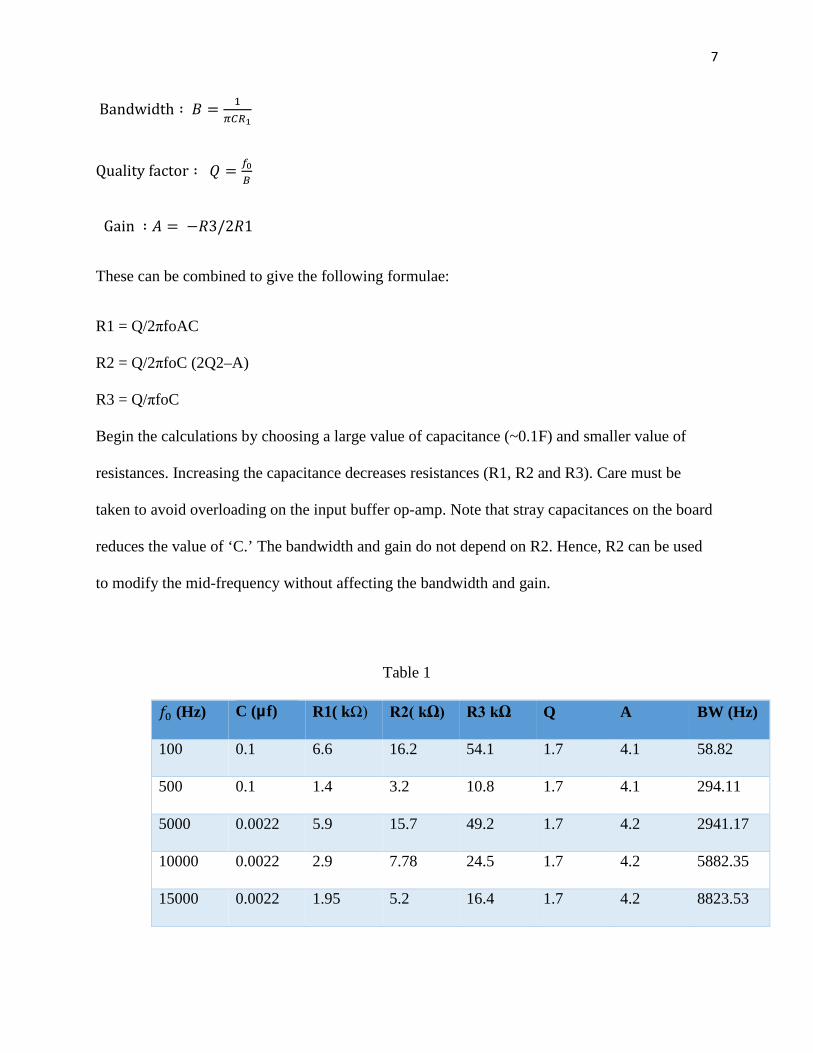
Begin the calculations by choosing a large value of capacitance (~0.1F) and smaller value of
resistances. Increasing the capacitance decreases resistances (R1, R2 and R3). Care must be
taken to avoid overloading on the input buffer op-amp. Note that stray capacitances on the board
reduces the value of ‘C.’ The bandwidth and gain do not depend on R2. Hence, R2 can be used
to modify the mid-frequency without affecting the bandwidth and gain.
Table 1
𝑓𝑓0 (Hz) C (µf) R1( kΩ) R2( kΩ) R3 kΩ Q A BW (Hz)
100 0.1 6.6 16.2 54.1 1.7 4.1 58.82
500 0.1 1.4 3.2 10.8 1.7 4.1 294.11
5000 0.0022 5.9 15.7 49.2 1.7 4.2 2941.17
10000 0.0022 2.9 7.78 24.5 1.7 4.2 5882.35
15000 0.0022 1.95 5.2 16.4 1.7 4.2 8823.53
8
Each stage of the op-amp needs to be capacitively coupled to the next stage so that the DC does
not get propagated and amplified. For a good low-frequency response, this coupling capacitor
should be greater than 1 F. A 10μF, 16V capacitor is used in each stage of the circuit here. The
circuit is powered by a 12V
DC regulated supply. Ground the Vcc pin of each op-amp with a 0.1μF ceramic disk capacitor to
bypass the noise.
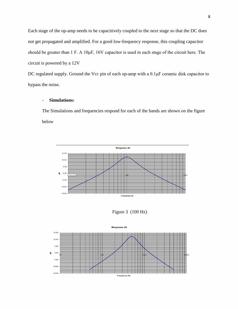
- Simulations:
The Simulations and frequencies respond for each of the bands are shown on the figure
below
Figure 3 (100 Hz)
9
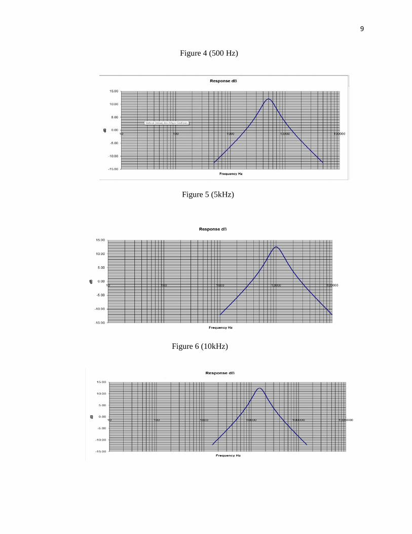
Figure 4 (500 Hz)
Figure 5 (5kHz)
Figure 6 (10kHz)
10
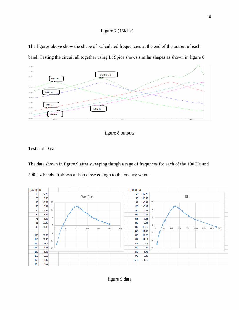
Figure 7 (15kHz)
The figures above show the shape of calculated frequencies at the end of the output of each
band. Testing the circuit all together using Lt Spice shows similar shapes as shown in figure 8
figure 8 outputs
Test and Data:
The data shown in figure 9 after sweeping throgh a rage of frequnces for each of the 100 Hz and
500 Hz bands. It shows a shap close eoungh to the one we want.
figure 9 data
11
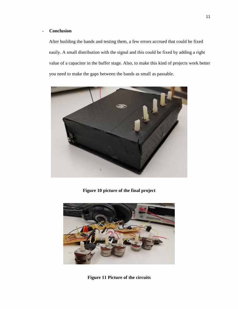
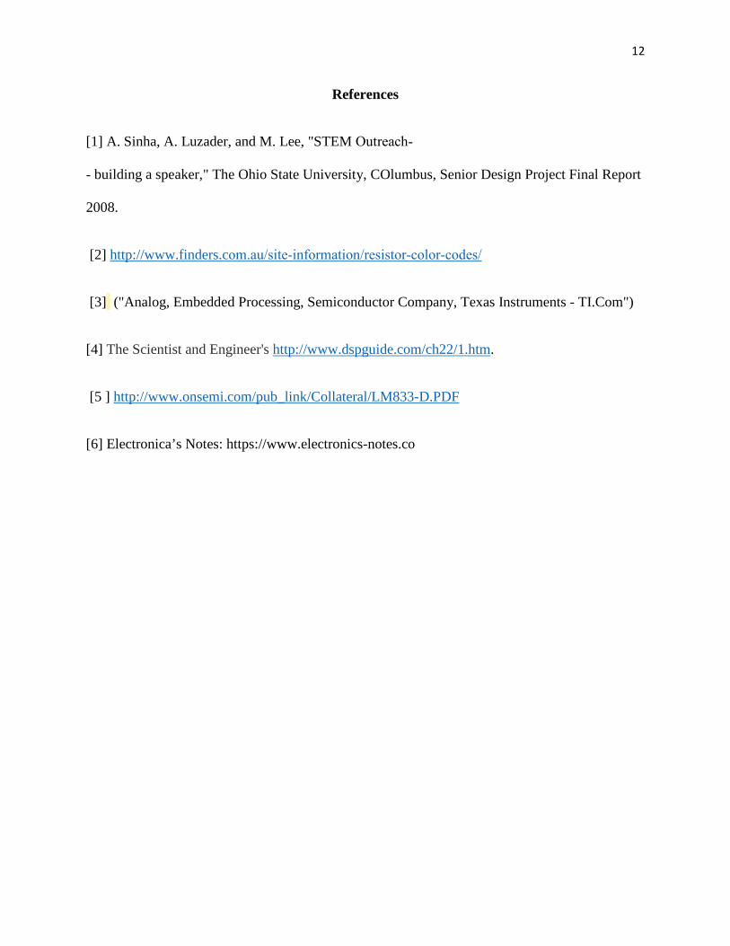
- Conclusion
After building the bands and testing them, a few errors accrued that could be fixed
easily. A small distribution with the signal and this could be fixed by adding a right
value of a capacitor in the buffer stage. Also, to make this kind of projects work better
you need to make the gaps between the bands as small as passable.
Figure 10 picture of the final project
Figure 11 Picture of the circuits
12
References
[1] A. Sinha, A. Luzader, and M. Lee, "STEM Outreach‐
‐ building a speaker," The Ohio State University, COlumbus, Senior Design Project Final Report
2008.
[2] http://www.finders.com.au/site‐information/resistor‐color‐codes/
[3] ("Analog, Embedded Processing, Semiconductor Company, Texas Instruments - TI.Com")
[4] The Scientist and Engineer's http://www.dspguide.com/ch22/1.htm.
[5 ] http://www.onsemi.com/pub_link/Collateral/LM833-D.PDF
[6] Electronica’s Notes: https://www.electronics-notes.co


![Bachpan'e Mustafa Wa Meelad'e Mustafa (Alehe Salat-O-Salam) [Urdu]](https://static.fdocuments.us/doc/165x107/577cb0ae1a28aba7118b45c4/bachpane-mustafa-wa-meelade-mustafa-alehe-salat-o-salam-urdu.jpg)


![UNDERGRADUATE RESEARCH PROJECT, EE497, 2015 … · UNDERGRADUATE RESEARCH PROJECT, EE497, 2015 1 ... found in reference [11]. (Note: If AVR Studio 5 doesn ... UNDERGRADUATE RESEARCH](https://static.fdocuments.us/doc/165x107/5add4f1d7f8b9a9d4d8cfdb7/undergraduate-research-project-ee497-2015-research-project-ee497-2015-1.jpg)