Memory Organization
31
The time delay of the five segments in a certain pipeline are as follows: t1=30 ns, t2=70 ns, t3=20 ns, t4=25 ns, t5=35 ns. The interface registers delay time tr=5 ns. How long would it take to add 100 pairs of numbers in the pipeline?. Solve the following question
-
Upload
surya-kameswari -
Category
Documents
-
view
91 -
download
0
description
chapter 12memory organizationmorris mano
Transcript of Memory Organization

The time delay of the five segments in a certain pipeline are as follows:
t1=30 ns,t2=70 ns,t3=20 ns,t4=25 ns,t5=35 ns.
The interface registers delay time tr=5 ns. How long would it take to add 100 pairs of numbers in the pipeline?.
Solve the following question

Memory Organization
12.1 Memory Hierarchy12.2 Main Memory12.3 Auxiliary Memory12.4 Associative Memory12.5 Cache Memory12.6 Virtual Memory12.7 Memory management hardware

Memory Hierarchy
The overall goal of using a memory hierarchy is to obtain the highest-possible average access speed while minimizing the total cost of the entire memory system.
Microprogramming: refers to the existence of many programs in different parts of main memory at the same time.

Main memory
ROM Chip

Memory Address Map
Memory Configuration (case study):
Required: 512 bytes ROM + 512 bytes RAM Available: 512 byte ROM + 128 bytes RAM
The designer of a computer system must calculate the amount of memory required for the particular application and assign it to either RAM or ROM.
The interconnection between memory and processor is then established from knowledge of the size of memory needed and the type of RAM and ROM chips available.
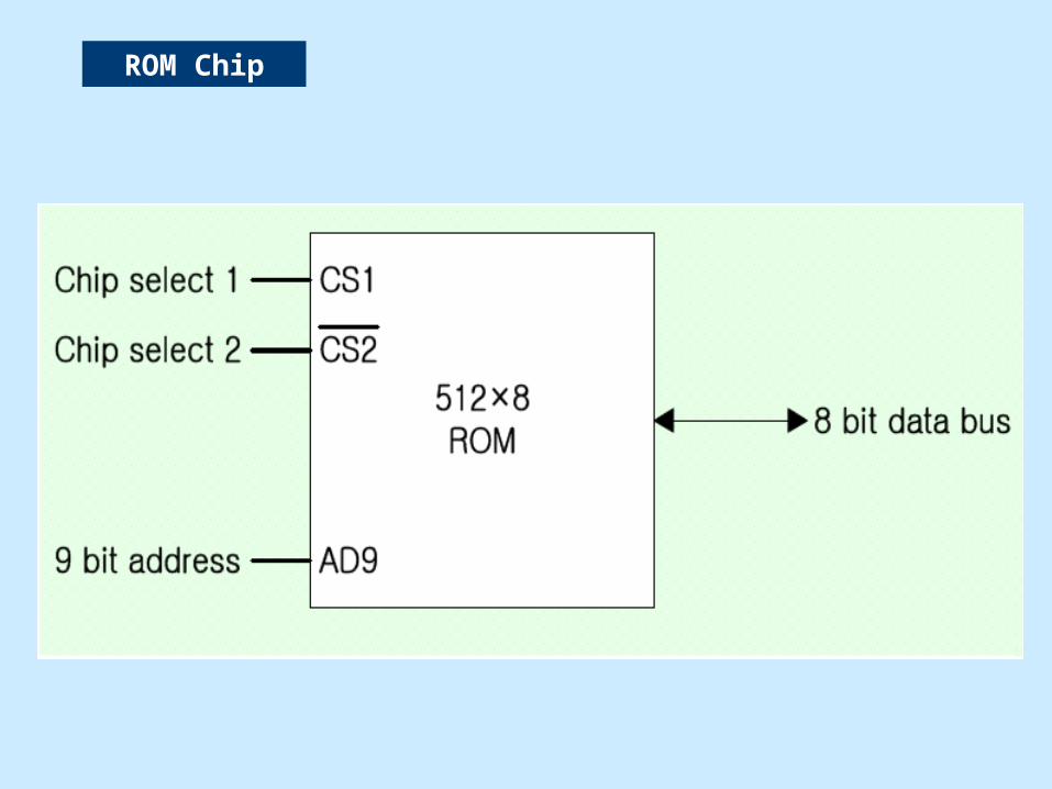
The addressing of memory can be established by meansof a table that specifies the memory address assigned to each chip.
The table, called a memory address map, is a pictorial representation of assigned address space for each chip in the system.
Memory Address Map

128×8RAM 1
CS1
AD7
WR
RD
CS2
128×8RAM 2
CS1
AD7
WR
RD
CS2
128×8RAM 4
CS1
AD7
WR
RD
CS2
128×8RAM 3
CS1
AD7
WR
RD
CS2
128×8ROM
CS1
CS2
AD9
Data
Data
Data
Data
Data
CPU
WRRD16 - 11 10 9 8 7 - 1
Address bus
Data bus
Decoder
3 2 1 0
1-7
8
9
Memory connections to the CPU

Associative Memory

Associative Memory
The time required to find an item stored in memory can be reduced considerably if stored data can be identified for access by the content of the data itself rather than by an address.
A memory unit access by content is called an associative memory or Content Addressable Memory (CAM). This type of memory is accessed simultaneously and in parallel on the basis of data content rather than specific address or location.
When a word is written in an associative memory, no address is given. The memory is capable of finding an empty unused location to store the word. When a word is to be read from an associative memory, the content of the word or part of the word is specified.
The associative memory is uniquely suited to do parallel searches by data association. Moreover, searches can be done on an entire word or on a specific field within a word. Associative memories are used in applications where the search time is very critical and must be very short.

Hardware Organization
Argument register (A)
Key register (K)
Associative memoryarray and logic
m words n bits per word
M
Matchregister
Input
Write
Read
Output

Associative memory of an m word, n cells per word
A1
C11
AnAj
K1 KnKj
C1j C1n
C i1 C ij C in
Cm1 Cmj Cmn
M1
Mm
Mi
Bit 1 Bit nBit j
Word 1
Word m
Word i

One Cell of Associative Memory
R S Matchlogic
Input
Read
Write
Output
To M i
K jA i
F ij

Neglect the K bits and compare the argument in A with the bits stored in the cells of the words.
Word i is equal to the argument in A if
Two bits are equal if they are both 1 or 0
For a word i to be equal to the argument in A we must have all xj variables equal to 1.
This is the condition for setting the corresponding match bit Mi to 1.
Match logic

Now include the key bit Kj in the comparison logic
The requirement is that if Kj=0, the corresponding bits of Aj and need no comparison. Only when Kj=1 must be compared. This requirement is achieved by OR ing each term with Kj
The match logic for word i in an associative memory can now be expressed by the following Boolean function.
If we substitute the original definition of xj, the above Boolean function can be expressed as follows:
Where is a product symbol designating the AND operation of all n terms.
Cont.

Match Logic cct.
F' i1 Fi1
A1K1
F' i2 Fi2
A2K2
F' in Fin
AnKn
M i

Read Operation
If more than one word in memory matches the unmasked argument field, all the matched words will have 1’s in the corresponding bit position of the match register.
It is then necessary to scan the bits of the match register one at a time. The matched words are read in sequence by applying a read signal to each word line whose corresponding Mi bit is a 1.
If only one word may match the unmasked argument field, then connect output Mi directly to the read line in the same word position,
The content of the matched word will be presented automatically at the output lines and no special read command signal is needed.
If we exclude words having zero content, then all zero output will indicate that no match occurred and that the searched item is not available in memory.

Write Operation
If the entire memory is loaded with new information at once, then the writing can be done by addressing each location in sequence.
The information is loaded prior to a search operation.
If unwanted words have to be deleted and new words inserted one at a time, there is a need for a special register to distinguish between active an inactive words.
This register is called “Tag Register.”
A word is deleted from memory by clearing its tag bit to 0.

Cache Memory

Cache Memory
Locality of reference
The references to memory at any given interval of time tent to be contained within a few localized areas in memory.
If the active portions of the program and data are placed in a fast small memory, the average memory access time can be reduced.
Thus, reducing the total execution time of the program. Such a fast small memory is referred to as “Cache Memory”.
The performance of the cache memory is measured in terms of a quality called “Hit Ratio”.
When the CPU refers to memory and finds the word in cache, it produces a hit. If the word is not found in cache, it counts it as a miss.
The ratio of the number of hits divided by the total CPU references to memory (hits + misses) is the hit ratio. The hit ratios of 0.9 and higher have been reported

The average memory access time of a computer system can be improved considerably by use of cache.
The cache is placed between the CPU and main memory. It is the faster component in the hierarchy and approaches the speed of CPU components.
When the CPU needs to access memory, the cache is examined. If it is found in the cache, it is read very quickly.
If it is not found in the cache, the main memory is accessed.
A block of words containing the one just accessed is then transferred from main memory to cache memory.
For example,
A computer with cache access time of 100ns, a main memory access time of 1000ns and a hit of 0.9 produce an average access time of 200ns. This is a considerable improvement over a similar computer without a cache memory, whose access time is 1000ns.
Cache Memory

The basic characteristic of cache memory is its fast access time. Therefore, very little or no time must be wasted when searching for words in the cache.
The transformation of data from main memory to cache memory is referred to as a “Mapping Process”.
There are three types of mapping procedures are available.
· Associative Mapping· Direct Mapping· Self – Associative Mapping.
Cache Memory

Consider the following memory organization to show mapping procedures of the cache memory .
·The main memory can stores 32k word of 12 bits each. ·The cache is capable of storing 512 of these words at any given
time. ·For every word stored in cache, there is a duplicate copy in main
memory. ·The CPU communicates with both memories
·It first sends a 15 – bit address to cache. ·If there is a hit, the CPU accepts the 12 bit data from cache
·If there is a miss, the CPU reads the word from main memory and the word is then transferred to cache.
Cache Memory

Associative Mapping
The associative mapping stores both the address and content (data) of the memory word.
A CPU address of 15 bits is placed in the argument register and associative memory is searched for a matching address.
If the address is found, the corresponding 12 bit data is read andsent to the CPU.
If no match occurs, the main memory is accessed for the word. The address – data pair is then transferred to associative cache memory.
If the cache is full, it must be displayed, using replacement algorithm. FIFO may be used.
Argument registerOctal
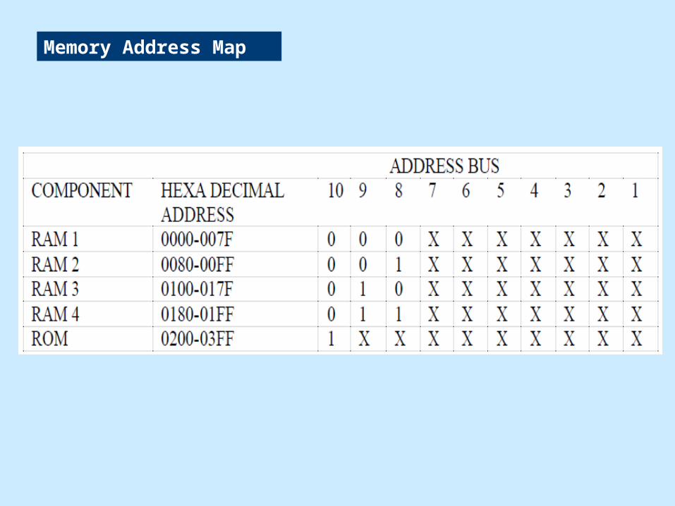
Direct Mapping
The 15-bit CPU address is divided into two fields.
The 9 least significant bits constitute the index field and the remaining 6 bits form the tag fields.
The main memory needs an address but includes both the tag and the index bits.
The cache memory requires the index bit only i.e., 9 bits.
There are 2k words in the cache memory & 2n words in the main memory.
e.g: k = 9, n = 15

Direct Mapping

00000
6710
Direct Mapping

Each word in cache consists of the data word and it associated tag.
When a new word is brought into cache, the tag bits store along data
When the CPU generates a memory request, the index field isused in the address to access the cache.
The tag field of the CPU address is equal to tag in the word from cache; there is a hit, otherwise miss.
How can we calculate the word size of the cache memory?
Direct Mapping

Set – Associative Mapping
In set – Associative mapping, each word of cache can store two or more words of memory under the same index address.
Each data word is stored together with its tag and the number of tag – data items in one word of cache is said to form a set.
Each index address refers to two data words and their associated tags.

Each tag requires 6 bits & each data word has 12 bits, so the word length is 2(6+12) =36 bits
An index address of 9 bits can accommodate 512 cache words. It can accommodate 1024 memory words.
When the CPU generates a memory request, the index value of the address is used to access the cache.
The tag field of the CPU address is compared with both tags in the cache.
Set – Associative Mapping
The most common replacement algorithms are:
·Random replacement ·FIFO
·Least Recently Used (LRU)

Writing into cache
Write-back method
Write-through method (The simplest & commonly used way)
there are two writing methods that the system can proceed.
update main memory with every memory write operation, with cache memory being update in parallel if it contains the word at the specified address.
This method has the advantage that main memory always contains the same data as the cache.
In this method only the cache location is updated during a write operation.
The location is then marked by a flag so that later when the word is removed from the cache it is copied into main memory.
The reason for the write-back method is that during the time a word resides in the cache, it may be updated several times.