
Computer Organization (Memory Organization)
29
Computer Organization (Memory Organization) KR Chowdhary Professor & Head Email: [email protected] webpage: krchowdhary.com Department of Computer Science and Engineering MBM Engineering College, Jodhpur November 14, 2013 KR Chowdhary Memory Sub-block 1/ 29
Transcript of Computer Organization (Memory Organization)

Computer Organization(Memory Organization)
KR ChowdharyProfessor & Head
Email: [email protected]
webpage: krchowdhary.com
Department of Computer Science and EngineeringMBM Engineering College, Jodhpur
November 14, 2013
KR Chowdhary Memory Sub-block 1/ 29

Memory
◮ Memory access may be synchronized by bus, or may work inasynchronous mode.
◮ Memory access time: time from req. to supply of data, memory
cycle time: delay time between two consecutive read requests.
n-bitaddress bus
n-bitdata bus
Control lines
(R/W, IO/M̄, etc)
MAR
MDR
Processor Memory
2n addresses
Word length=n bits
Figure 1: Connection of memory to processor
◮ Virtual memory:?
KR Chowdhary Memory Sub-block 2/ 29
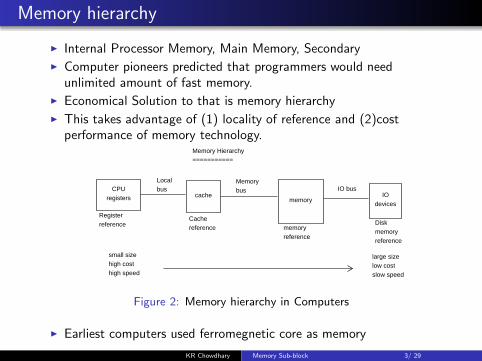
Memory hierarchy
◮ Internal Processor Memory, Main Memory, Secondary
◮ Computer pioneers predicted that programmers would needunlimited amount of fast memory.
◮ Economical Solution to that is memory hierarchy
◮ This takes advantage of (1) locality of reference and (2)costperformance of memory technology.
CPUregisters cache
memoryIO
devices
Registerreference
Cachereference memory
reference
Diskmemoryreference
Memorybus IO bus
Memory Hierarchy===========
small sizehigh costhigh speed
large sizelow costslow speed
Localbus
Figure 2: Memory hierarchy in Computers
◮ Earliest computers used ferromegnetic core as memory
KR Chowdhary Memory Sub-block 3/ 29
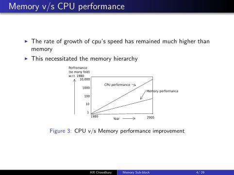
Memory v/s CPU performance
◮ The rate of growth of cpu’s speed has remained much higher thanmemory
◮ This necessitated the memory hierarchy
Figure 3: CPU v/s Memory performance improvement
KR Chowdhary Memory Sub-block 4/ 29

Some characteristics
◮ Cost(c): If C is total cost ofmemory system of size S (forstorage + access), c = C
S
dollars per bit.
◮ Access time: tA is timebetween request made, toinformation delivered.bA = w/tA is access rate inbits/sec(Band Width).
◮ Access mode: (1) Randomaccess memory (RAM), (2)Serial access memory.
◮ Random: RAM is costlybecause every location hasseparate access mechanism.
◮ For serial access: accessmechanism is shared betweenmany locations. Some diskdrives are semi-random, i.e.,(direct access) - R/W heads ofall recording surfaces accessthem all simultaneously
◮ Other classes:(1)non-volatile/volatile -datais lost if power removed, (2)static /dynamic memories -requires frequent refreshing.
◮ Non-destructive/Destructivereadout - every read operationis followed with write.
KR Chowdhary Memory Sub-block 5/ 29

Access mechanisms
Read/write head selector
R/W heads
storage locations
Conceptual model of randm access memory
motion
storage locations
R/W head
Conceptionalmodel of a serialaccess memory
DRO
DestrictiveRead
NDRO bufferRegister
RestoringWrite
Disk
Figure 4: Random and serial access.
KR Chowdhary Memory Sub-block 6/ 29
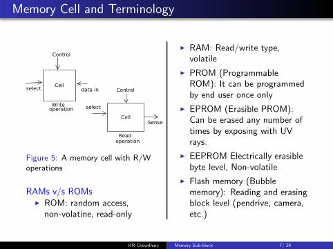
Memory Cell and Terminology
Figure 5: A memory cell with R/Woperations
RAMs v/s ROMs◮ ROM: random access,
non-volatine, read-only
◮ RAM: Read/write type,volatile
◮ PROM (ProgrammableROM): It can be programmedby end user once only
◮ EPROM (Erasible PROM):Can be erased any number oftimes by exposing with UVrays.
◮ EEPROM Electrically erasiblebyte level, Non-volatile
◮ Flash memory (Bubblememory): Reading and erasingblock level (pendrive, camera,etc.)
KR Chowdhary Memory Sub-block 7/ 29

ROM v/s Flash memories
Applications of ROM:◮ Microprogramming, stores
library subroutines forfrequently used functions,Boot ROMs, Function tables,Modest size programs anddata are kept in ROMs,System programs, Data arewired as part of the fabricationprocess
Figure 6: 1-bit ROM Cell.
Flash Memories:
◮ Read, write, erase: Block byblock
◮ There is no byte levelstructure like other memories
◮ One transistor per bit provideshigher density.
◮ Stores information in floatinggate transistors. Does notdischarge for many years.
◮ ADV: Low power dissipation,non-volatile, compact,alternate to CD and HDD.
◮ Disadv: Slow speed.
KR Chowdhary Memory Sub-block 8/ 29

Some properties of memories
◮ Cycle-time and data transferrate: The definition of tA isnot applicable for dynamicRAMs. The minimum timebetween two memory requestsis > tA due to refreshing cycle.The time between twoconsecutive memory reads iscalled the cycle time ofmemory (tM).
◮ Memory Latency (L):= Delayfrom request by processor todelivery of word from memory.Bandwidth (BW)=w
L. If R is
no. of requests which can beserved simultaneously, thenBW = R∗w
L.
◮ Ideal memory: Infinitecapacity, zero latency, infinitebandwidth, which are notachievable practically.
◮ But, Memory hierarchyprovides decreased latency,hence does require high BW .In addition, the Parallelinterleaved memory helps toincrease the BW .
KR Chowdhary Memory Sub-block 9/ 29

Dynamic RAM Memory structures
Figure 7: 1-bit DRAM Cell.
Over a time (of msecs.) thecapacitor holding 1/0 getsdischarged, hence requiresrefreshing.
◮ The address line is to beactivated for read/write
operation. The transistor actsas switch.
◮ Combination of Bit line ’1/0’and address line high, causeswriting ’1/0’ at the selectedcell.
◮ For memory Read, address linehigh will select the cell, storedvalue is sensed, amplified andsent at output of senseamplifier.
◮ Read operation is destructive,hence capacitor charge needsto be rebuilt periodically(refreshing).
KR Chowdhary Memory Sub-block 10/ 29
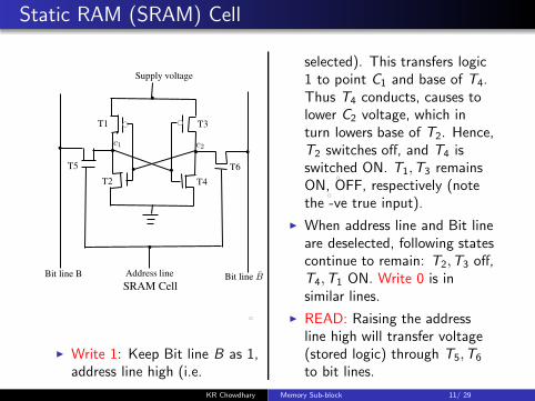
Static RAM (SRAM) Cell
b
b
Supply voltage
Address lineBit line B Bit line B̄
T1
T2
T3
T4
T5 T6
SRAM Cell
c1 c2b
b
b
b bb
bc
bc
bc
bcbc
◮ Write 1: Keep Bit line B as 1,address line high (i.e.
selected). This transfers logic1 to point C1 and base of T4.Thus T4 conducts, causes tolower C2 voltage, which inturn lowers base of T2. Hence,T2 switches off, and T4 isswitched ON. T1,T3 remainsON, OFF, respectively (notethe -ve true input).
◮ When address line and Bit lineare deselected, following statescontinue to remain: T2,T3 off,T4,T1 ON. Write 0 is insimilar lines.
◮ READ: Raising the addressline high will transfer voltage(stored logic) through T5,T6
to bit lines.
KR Chowdhary Memory Sub-block 11/ 29

SRAM v/s DRAM
◮ Both volatile
◮ DRAMs require refreshingcircuit because the storedcharge in capacitor decayswith time. Also, the readoperations is destructive,hence needs re-writing.
◮ Refreshing circuit’s cost is
high for small size DRAMs.Hence, DRAMs are preferredfor large capacities.
◮ SRAMs are faster thanDRAMs. Due to cost andspeed SRAMs are used incaches, and DRAMs are usedfor RAM (Main Memory).
KR Chowdhary Memory Sub-block 12/ 29
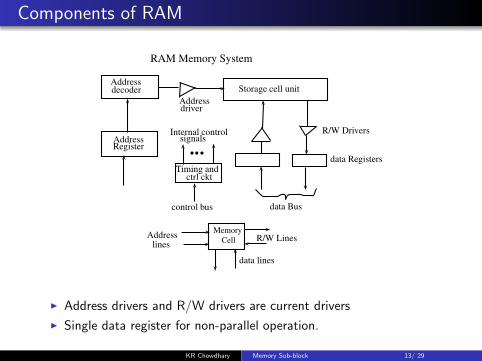
Components of RAM
b b b
Addresslines
R/W Lines
data lines
Memory
RAM Memory System
Addressdecoder Storage cell unit
R/W Drivers
data Registers
data Bus
Timing andctrl ckt
AddressRegister
Addressdriver
control bus
Internal controlsignals
Cell
◮ Address drivers and R/W drivers are current drivers
◮ Single data register for non-parallel operation.
KR Chowdhary Memory Sub-block 13/ 29

On/Two dimensional RAM
Address bus
address drivers
One dimensional storage
storage cell
Ad
dress
Deco
der
size = n lines
Total locations = 2n
cn − 1
c0
Figure 8: One Dimensional RAM
IF no. of address lines are n, thentotal 2n words can be stored.
Xad
dress
deco
der
Y address decoder
Memory cells
Address lines
X Y
Figure 9: Two Dimensional RAM
IF no. of address lines are x+ y ,for horizontals and vertical addressdecoders then total 2x × 2y wordscan be stored.
KR Chowdhary Memory Sub-block 14/ 29
DRAM with refreshing
bb
CE
WE
OERDY
Refreshcounter
Row addrcounter
Address
A0
A6
Refreshtimer and
column adrbuffer
databuffer
col. adr decoder
Memory cell
array
Intell 2186 8k x 8-bit DRAM
arbiter
MUX
controllogic
A7 A12 I/O0 I/O7
b b bb b b
bbb
b b b b b
Row
add
ressd
ecod
er
Figure 10: Two Dimensional RAM
Refreshing is interleaved with memory R/W operations.
KR Chowdhary Memory Sub-block 15/ 29

DRAM with refreshing
◮ All cells are refreshed onceevery 2 msec. All 128 row areread and recharged to originallogic 1/ 0.
◮ Refreshing is automaticallytriggered by an interval timer.All 128 rows are refreshed in128 x 500 nsec. = 64 µ sec.Since refresh is interleavedwith R/W, max. delay in anyR/W is only 500 nsec. Thedelay is taken care of by RDYline.
◮ Since all cells are refreshed in2 msec., the fraction time isonly 64µ sec
2msec≃ 3.2 percent.
◮ An arbiter selects the rowaddress 0-127.
◮ If memory access time is tA,and read starts at time t0,then data is made available att0+ tA time if no refresh cycleexists with current read cycle,otherwise it is made availableat time t0+ tA+ 500(nsec).
KR Chowdhary Memory Sub-block 16/ 29

Serial Access Memories
◮ Finds their applications in bulkstorage, with per bit cost low.Information is stored in tracks,where each cell stores one bit ofinformation. A specified item isaccessed by moving R/W head ormedium, or both. Conceptuallythese are shift registers withlimited access points.
◮ ts : Seek time: - time to moveR/W head from one track toanother.
◮ tl : Latency time: - time to reachto data location, once the headhas reached to the desired track.
◮ A word of w-bits may be stored
serially on a track or it can bestored on |w | tracks, reading allin parallel.
◮ Data transfer rate: Bit rate atwhich information can betransferred to/from the track.
◮ For each track of N-words,rotation speed (of disk) of rrotations per sec., n is number ofwords per block, the data rate ofmemory if rN words per sec.Once the head is positioned, ablock can be transferred inn(rN)−1 secs. The appox timeto transfer a block:tB = ts + tl +n(rN)−1.
KR Chowdhary Memory Sub-block 17/ 29
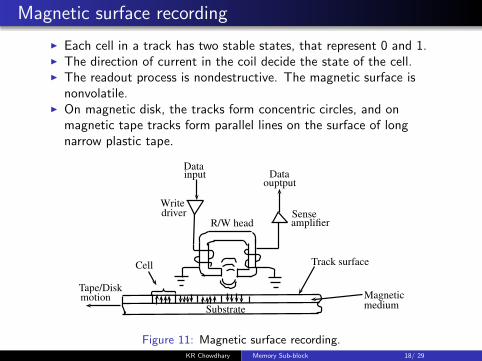
Magnetic surface recording
◮ Each cell in a track has two stable states, that represent 0 and 1.◮ The direction of current in the coil decide the state of the cell.◮ The readout process is nondestructive. The magnetic surface is
nonvolatile.◮ On magnetic disk, the tracks form concentric circles, and on
magnetic tape tracks form parallel lines on the surface of longnarrow plastic tape.
Dataouptput
Datainput
Senseamplifier
Writedriver
Track surface
Magneticmedium
R/W head
Cell
Substrate
Tape/Diskmotion
Figure 11: Magnetic surface recording.KR Chowdhary Memory Sub-block 18/ 29
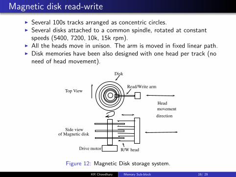
Magnetic disk read-write
◮ Several 100s tracks arranged as concentric circles.◮ Several disks attached to a common spindle, rotated at constant
speeds (5400, 7200, 10k, 15k rpm).◮ All the heads move in unison. The arm is moved in fixed linear path.◮ Disk memories have been also designed with one head per track (no
need of head movement).
Disk
Read/Write arm
R/W headDrive motor
Top View
Side viewof Magnetic disk
Head
movement
direction
Figure 12: Magnetic Disk storage system.
KR Chowdhary Memory Sub-block 19/ 29
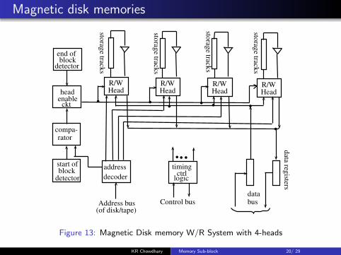
Magnetic disk memories
R/WHead
R/WHead
R/WHead
R/WHead
bb
Control busAddress bus
end ofblock
detector
headenable
ckt
compa-
start ofblock
detector
address
decoder
timingctrl
logic
storag
etrack
s
rator
databus
data
registers
bbb
b
b
b
b b
(of disk/tape)
storag
etrack
s
storag
etrack
s
storag
etrack
s
Figure 13: Magnetic Disk memory W/R System with 4-heads
KR Chowdhary Memory Sub-block 20/ 29
Magnetic disk memory system
◮ Output of address decoderdetermines: (1) track to beused, and (2) location ofdesired block of information inthe track (i.e., block address).The steps of Disk R/W are:
1. Track address determinesparticular R/W head
2. The head is moved on tothe track.
3. Some track positionindicator is needed, which isgenerated when the trackpasses under the R/W
head.
4. The generated address iscompared with the blockaddress produced by theaddress decoder.
5. When they match, theselected head is enabledand data transfer begins.
6. The R/W head is disabledwhen complete block ofinformation is transferred.
◮ The memory input and outputregisters are shift registers ofparallel/serial I/O data.
KR Chowdhary Memory Sub-block 21/ 29

Magnetic disk memory typical data:
NEC D2257
No. of recording surfaces 8No. of tracks per recording surface 1024no. of R/W heads per recording surface 1Track recording density 9420 bits/in.Storage capacity of track 20,480 bytesTotals Storage capacity of disk drive 167.7M bytesDisk rotation speed 3510 rpmAverage seek time 20 msAverage latency 8.55 msData transfer rate 1.198 bits/s
KR Chowdhary Memory Sub-block 22/ 29

Magnetic tape memories
b
b
b b
b
b
b b
capstons
Tape reels
R/W head
tapeloops
Idlers
Figure 14: Magnetic tape storage.
◮ Compact inexpensive portablemedium for storing large amountinformation. Information isstored in binary, unlike audio andvideo tapes, in 9 parallel tracks.
(basic memory word is 9-bits:8-bit info+ 1 parity bit).
◮ Packed in cartridges/cassettes;resemble audio tapes. Medium isnot in continuous motion. Whenrequest recved, tape is movedforward/ backward to desiredlocation.
◮ Loops for rapid start-stop.Capstans accelerate tape. Laterit moves at tape speed, at whichthe data transfer takes place.
◮ Typical storage density: 1600bytes/in., speed 18.75 in./s.Thus, data tr. rate = 1600 *18.75 = 30,000 bytes/s. Info.stored in blocks with block gap.Rewind time ≈ 1 min.
KR Chowdhary Memory Sub-block 23/ 29

Some other characteristics
◮ Storage density, per unit area
◮ Energy consumption (may or may not require cooling)
◮ Reliability: MTBF (mean time between failures)
◮ Maximum Number of read/write operations (life-time)
KR Chowdhary Memory Sub-block 24/ 29

Exercises
1. 1.1 How many 128×8 RAM chips are required to provide a memorycapacity of 2048 bytes?
1.2 How many address lines are required for accessing 2048 bytes? Howmany chips are common for all the chips?
1.3 How many lines must be decoded for chip-select? Specify the size ofchip select?
2. What is transfer rate of 8-track magnetic tape whose speed is 120inches per sec. and whose density is 1600 bits per inch?
3. Consider a dynamic RAM that must be given a refresh cycle of 64times per msec. Each refresh operation requires 100 ns. A memorycycle requires 200 nsec. What percentage of the memory’s totaloperating time must be given to refreshes?
4. The memory of a particular microcomputer is built from 128k X 1DRAMs. According to the data-sheet, the cell array of the DRAM isorganized into 512 rows. Each row must be refreshed at least onceevery 4 ms. Suppose we refresh memory on a strictly periodic basis.
4.1 What is the time period between successive refresh requests?4.2 How long a refresh address counter do we need?
KR Chowdhary Memory Sub-block 25/ 29

Exercises
5. A certain moving arm disk-storage device has the following specs.No. of tracks per recording surface 200Disk rotation speed 2400 rpmTrack storage capacity 62,500 bits
Estimate the average latency and the data transfer rate of thisdevice.
6. A magnetic-tape system accommodates 2400-ft reels of standardnine-track tape. The tape is moved past the recording head at arate of 200 in./s.
6.1 What must the linear tape-recording density be in order to achieve adata-transfer rate of 107 bits/s?
6.2 Suppose that the data on the tape is organized into blocks eachcontaining 32k bytes. A gap of 0.3 in. separates each block. Howmany bytes may be stored on the tape?
KR Chowdhary Memory Sub-block 26/ 29

Exercises
7. Figure 15 shows a simplified timing diagram of a DRAM readoperation over a bus. The access time is considered to last from t1to t2. Then there is a recharge time, lasting from t2 to t3, duringwhich the DRAM chips will have to recharge before the processorcan access them again.7.1 Assume that the access time is 60 ns and recharge time is 40 ns.
What is the memory cycle time? What is the maximum data ratethis DRAM can sustain, assuming a 1-bit output?
7.2 Constructing a 32-bit wide memory system using these chips yieldswhat data transfer? (RAS=row addr select, CAS=col. addr select)
Addr. lines
RAS
CAS
R/W̄
Data lines data valid
t1 t2 t3
row addr col. addr.
Figure 15: Timing diagram of DRAM.
KR Chowdhary Memory Sub-block 27/ 29

Exercises
8. The memory of a particular microcomputer is built from 128K × 1DRAMs. According to the data sheet, the cell array of DRAM isorganized into 512 rows. Each row must be refreshed atleast onceevery 4 ms. Suppose we refresh memory on a strictly periodic basis:
8.1 What is the time period between successive refresh requests?8.2 How long a refresh address counter do we need?
9. Design a 16 X 4-bits RAM using 4X2-bits ICs.
10. Design a 16-bit memory of total capacity 8192 bits using SRAMchips of 64× 1 bits. Give the array configuration of the chips on thememory board showing all required input and output signals forassigning this memory to the lowest address space. The designshould allow for both byte and 16-bit word accesses.
KR Chowdhary Memory Sub-block 28/ 29
Bibliography
John P. Hayes, “Computer Architecture and Organization”, 2ndEdition, McGraw-Hill, 1988. (chapter 5)
William Stalling, “Computer Organization and Architecture”, 8thEdition, Pearson, 2010. (chapter 5)
KR Chowdhary Memory Sub-block 29/ 29


![CS 104 Computer Organization and Design...Computer Organization and Design Memory Hierarchy CS104: Memory Hierarchy [Adapted from A. Roth] 2 Memory Hierarchy • Basic concepts •](https://static.fdocuments.us/doc/165x107/60a6b4852c2f420e7342dd30/cs-104-computer-organization-and-design-computer-organization-and-design-memory.jpg)


