Memory Management and Access - Academia … 3_Parte 1... · 3.1. Memory maps Memory map It refers...
60
Department of Electronics Academic Year 14/15 (ver 25-10-2014) Topic 3 Memory Management and Access
Transcript of Memory Management and Access - Academia … 3_Parte 1... · 3.1. Memory maps Memory map It refers...

ARM Cortex M3(i)
Department of Electronics Academic Year 14/15
(ver 25-10-2014)
Topic 3
Memory Management and Access
3.1. Memory maps 3.2. Memory expansion 3.3. Memory management & Data alignment 3.4. Design of a memory map 3.5. Access management and timing 3.6. Cortex-M3 Memory Map 3.7. The External Memory Controller (EMC) 3.8. The Memory Protection Unit (MPU)
Index
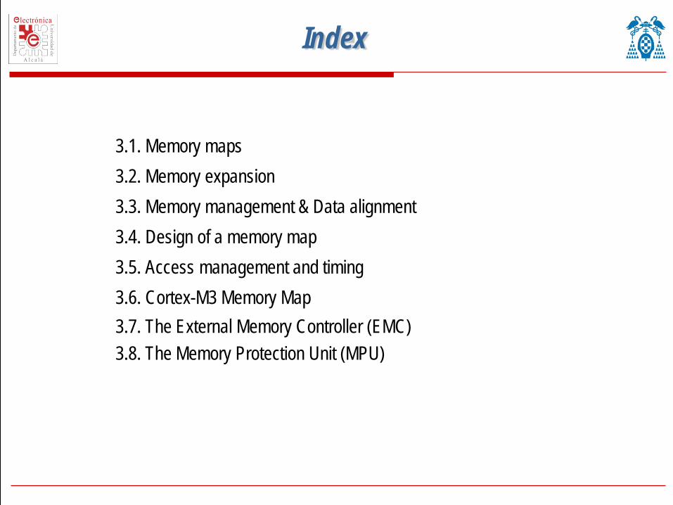
3.1. Memory maps
Memory map It refers to the organization of the different memory units in the uP address space
uP address space Number of addresses: 2m positions (addresses), being m the size of the address bus
Width word n bits, being n the number of lines (bits) of the data bus
uP address space: 2m X n

3.1. Memory maps
The memory map specification can be carried out as follows:
Functional: it describes the allocation (addresses) of the different elements (hardware or software) of the digital system, according to their function: the location of the program sections, general data and data tables, interface registers, etc.
Physical: it describes the address correspondence between the map and the physical device which implement it. All the connections between the devices will be carried out (taking into account the structure of the address bus and data bus, the method of selecting devices, etc.)
By means of the memory map, it is described which addresses are occupied by the different devices assigned to specific functions
Conceptual elements included in the map: Program memory (typically non-volatile memories) Data memory (can be volatile and non-volatile memories) Input/output space. All the interfaces according to the peripherals that will be needed
have to be included in the map To sum up, the memory map typically includes ROM, RAM and I/O interfaces
3.1. Memory maps
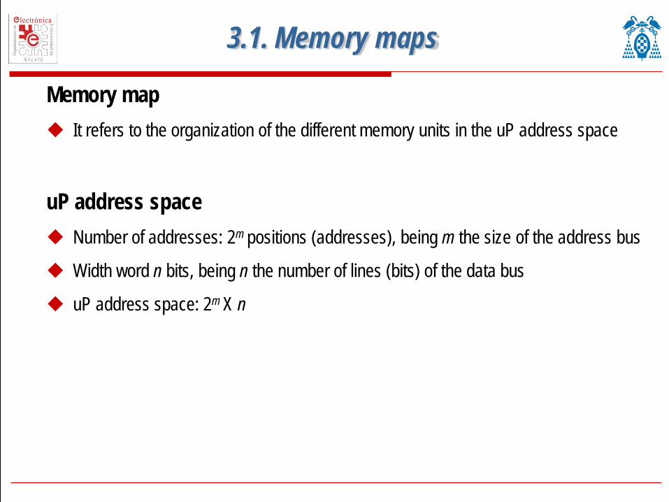
In the design of the map, it is specified which addresses are occupied by the different devices, indicating: The starting address, usually called base address
The last address. It is calculated as: base address+number of positions occupied by the device in memory
Considerations about the base address, Could it be any value? 1. It has to belong to the uP address space (logically)
2. It has to be an appropriate value, so the last address is inside the address space
3. It has to be multiple of the size of the memory block that has to be addressed: if it is needed to map a M bytes block, the address base has to be multiple of M
Example: for a 8Kbytes block, the address base could be 0x0000, 0x2000, 0x4000 … • The 0 address is multiple of any block
• There is a “trick”. The address base finishes always in a determined number of 0 (how many?)
3.1. Memory maps
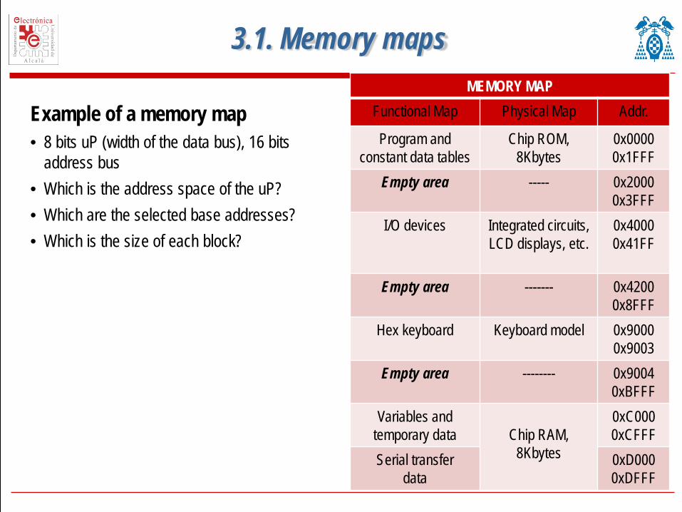
Example of a memory map • 8 bits uP (width of the data bus), 16 bits
address bus • Which is the address space of the uP? • Which are the selected base addresses? • Which is the size of each block?
MEMORY MAP Functional Map Physical Map Addr.
Program and constant data tables
Chip ROM, 8Kbytes
0x0000 0x1FFF
Empty area ----- 0x2000 0x3FFF
I/O devices Integrated circuits, LCD displays, etc.
0x4000 0x41FF
Empty area ------- 0x4200
0x8FFF Hex keyboard Keyboard model 0x9000
0x9003 Empty area -------- 0x9004
0xBFFF Variables and
temporary data
Chip RAM, 8Kbytes
0xC000 0xCFFF
Serial transfer data
0xD000 0xDFFF
3.2. Memory Expansion Goal: To obtain a block of memory of larger capacity by using basic memory chips
(usually of the same capacity), with two purposes: To provide a memory block of larger capacity. To adapt to the specifications of the selected uP (data bus and/or address space)
Reminder: Capacity=number of words X size of each word
Capacity increases if one of the parameters (or both) increases
Types of memory expansions: To increase the size of the word (it means to increase the number of bits per word) To increase the number of words Both of them

Expansion of the number of bits per word (word length) Conceptually it means to increase the width of the data bus in the new memory block. How
many bits? Each time the memory block is accessed, all the memory chips are simultaneously activated
(the data is “shared” among all the chips) The size of the address bus is held
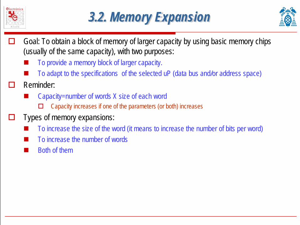
3.2. Memory Expansion
Memory 1Kx4
Memory 1Kx4
Memory 1Kx4
A[9:0] D[3:0]
Memory of 1Kx8
A[9:0] D[7:0]
3.2. Memory Expansion
Memory 1Kx4
A[9:0] D[3:0]
Memory 1Kx4
Memory 1Kx4
Memory 2Kx4
A[10:0] D[3:0]
Expansion of the number of words Conceptually it means to increase the size of the address bus
How many bits? (the number of bits is increased always in power of two) The width of the data bus is held
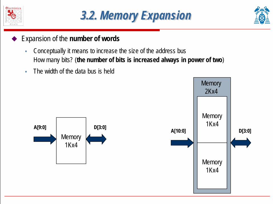
Combination of both expansions, to increase the number of bits per word, and the number of words: The width of the data bus is increased The address bus size is increased
3.2. Memory Expansion
Memory 1Kx4
Memory 1Kx4
Memory 1Kx4
A[9:0] D[3:0]
Memory de 2Kx8
Memory 1Kx4
Memory 1Kx4
A[10:0] D[7:0]

How is the memory connected to the uP? The resulting expanded memory has to be connected as if it was only one chip,
connecting the suitable lines of the data, address and control busses.
3.2. Memory Expansion
Example: 64Kbytes memory RAM • Address: 16 lines, e.g. A0-A15
(there are other solutions) • Data: 8 lines • Control: operation line(R/#W),
address validation (#AS)
Control bus
Address bus
Data bus
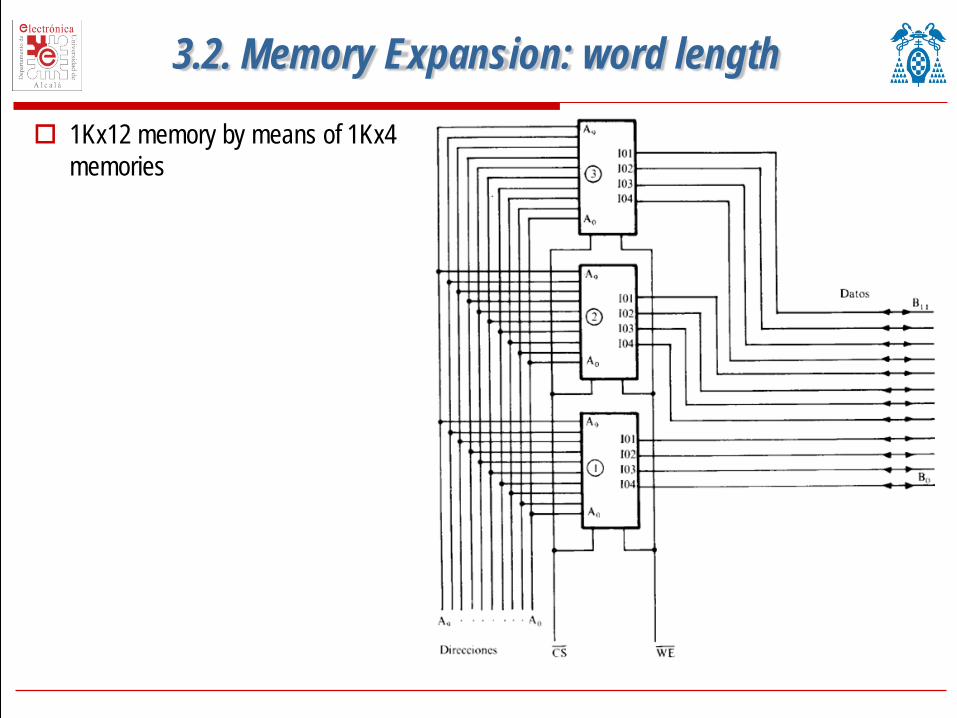
1Kx12 memory by means of 1Kx4 memories
3.2. Memory Expansion: word length
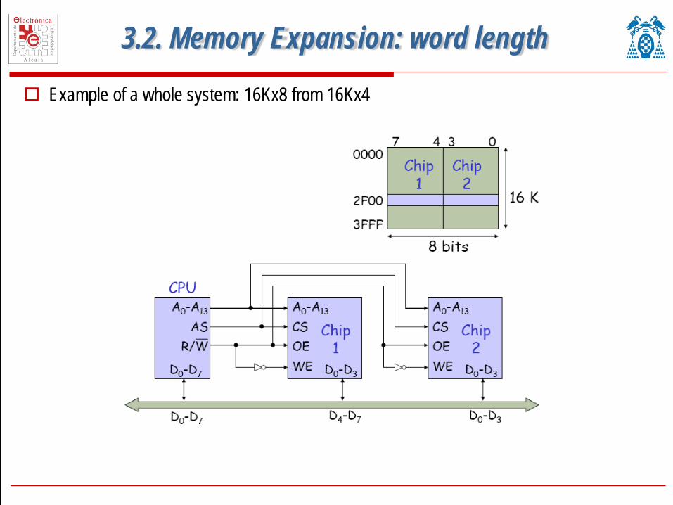
Example of a whole system: 16Kx8 from 16Kx4
3.2. Memory Expansion: word length

Example of a whole system: 16Kx8 from 4Kx8
3.2. Memory Expansion: number of words
Question: Deduct the address range that implements each chip, if the memory address busses are connected to A2-A13, and for decoding are used A0 and A1
Address
Data
Design a 2Kx4 memory block by means of 1Kx4 memory chips
3.2. Memory Expansion: number of words
Which is the address range of each chip?
If A0 is used for selecting each chip (the memory address bus is connected from the uP A1 line), which is the address range of each chip?
Example 1
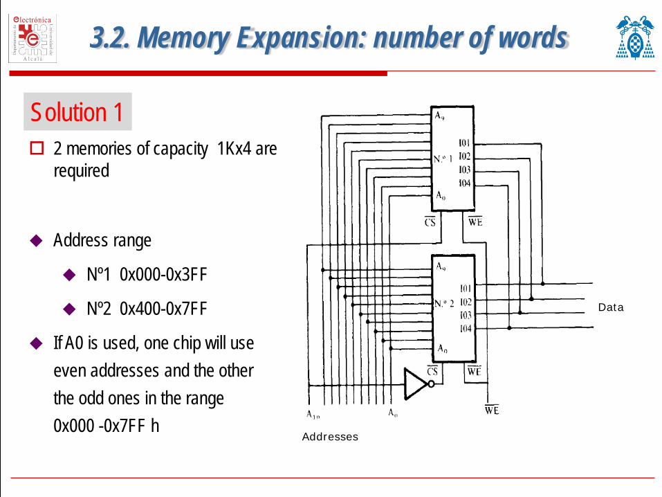
2 memories of capacity 1Kx4 are required
3.2. Memory Expansion: number of words
Address range
Nº1 0x000-0x3FF
Nº2 0x400-0x7FF
If A0 is used, one chip will use even addresses and the other the odd ones in the range 0x000 -0x7FF h
Solution 1
Addresses
Data
Design a 20Kx8 memory block by means of 4Kx8 memory chips. For decoding, a 3/8 decoder has to be used
3.2. Memory Expansion: number of words
Which is the address range of each chip?
For which capacity has the expansion been designed?
Example 2
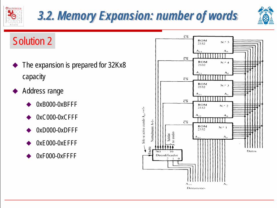
3.2. Memory Expansion: number of words
The expansion is prepared for 32Kx8 capacity
Address range 0xB000-0xBFFF
0xC000-0xCFFF
0xD000-0xDFFF
0xE000-0xEFFF
0xF000-0xFFFF
Solution 2
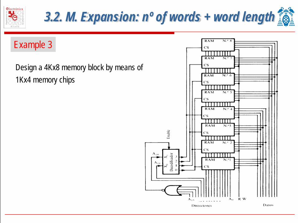
3.2. M. Expansion: nº of words + word length
Example 3
Design a 4Kx8 memory block by means of 1Kx4 memory chips
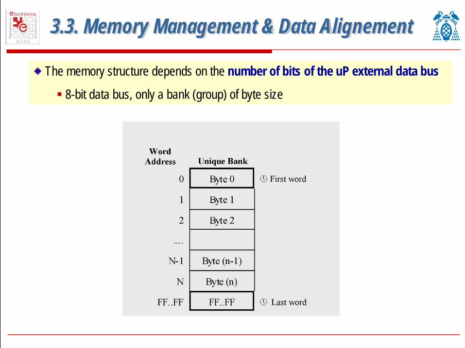
The memory structure depends on the number of bits of the uP external data bus
8-bit data bus, only a bank (group) of byte size
3.3. Memory Management & Data Alignement
Dirección dela palabra Banco Par Banco Impar
0 Byte 0 Byte 1 » Primera palabra
2 Byte 2 Byte 3
....
N-2 Byte (n-2) Byte (n-1)
N Byte (n) Byte (n+1)
FF..FE FF..FE FF..FF » Última palabra
Dirección dela palabra Banco Par Banco Impar
0 Byte 0 Byte 1 » Primera palabra
2 Byte 2 Byte 3
....
N-2 Byte (n-2) Byte (n-1)
N Byte (n) Byte (n+1)
FF..FE FF..FE FF..FF » Última palabra
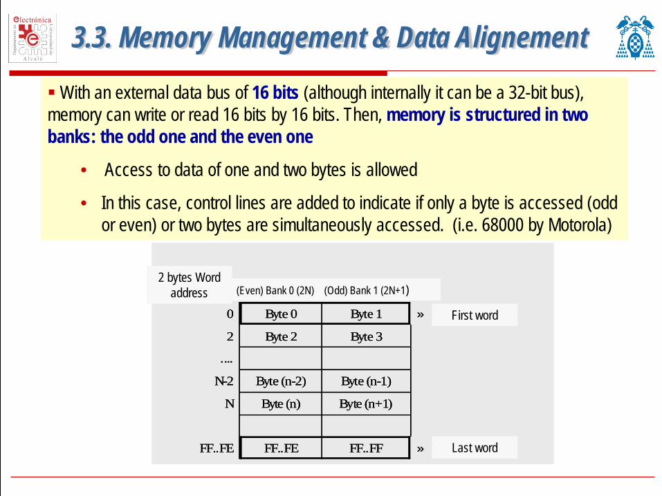
(Even) Bank 0 (2N) (Odd) Bank 1 (2N+1)
First word
Last word
2 bytes Word address
With an external data bus of 16 bits (although internally it can be a 32-bit bus), memory can write or read 16 bits by 16 bits. Then, memory is structured in two banks: the odd one and the even one
• Access to data of one and two bytes is allowed
• In this case, control lines are added to indicate if only a byte is accessed (odd or even) or two bytes are simultaneously accessed. (i.e. 68000 by Motorola)
3.3. Memory Management & Data Alignement
3.3. Memory Management & Data Alignement
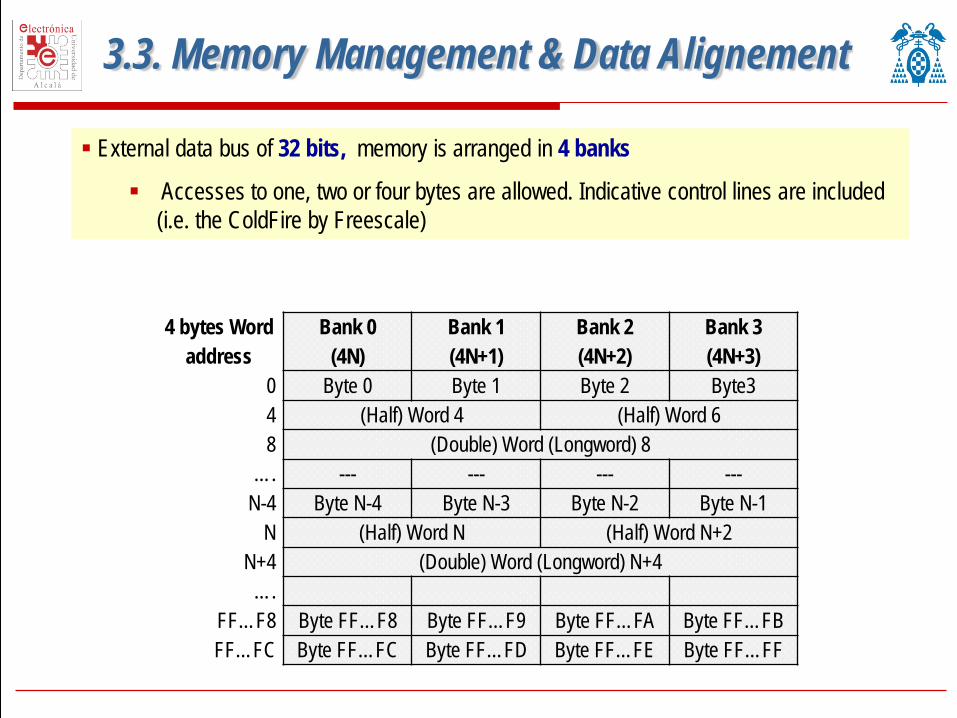
External data bus of 32 bits, memory is arranged in 4 banks
Accesses to one, two or four bytes are allowed. Indicative control lines are included (i.e. the ColdFire by Freescale)
4 bytes Word address
Bank 0 (4N)
Bank 1 (4N+1)
Bank 2 (4N+2)
Bank 3 (4N+3)
0 Byte 0 Byte 1 Byte 2 Byte3 4 (Half) Word 4 (Half) Word 6 8 (Double) Word (Longword) 8
…. --- --- --- --- N-4 Byte N-4 Byte N-3 Byte N-2 Byte N-1
N (Half) Word N (Half) Word N+2 N+4 (Double) Word (Longword) N+4
…. FF…F8 Byte FF…F8 Byte FF…F9 Byte FF…FA Byte FF…FB FF…FC Byte FF…FC Byte FF…FD Byte FF…FE Byte FF…FF
3.3. Memory Management & Data Alignement
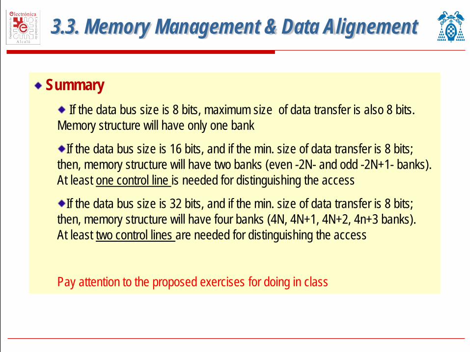
Summary If the data bus size is 8 bits, maximum size of data transfer is also 8 bits.
Memory structure will have only one bank
If the data bus size is 16 bits, and if the min. size of data transfer is 8 bits; then, memory structure will have two banks (even -2N- and odd -2N+1- banks). At least one control line is needed for distinguishing the access
If the data bus size is 32 bits, and if the min. size of data transfer is 8 bits; then, memory structure will have four banks (4N, 4N+1, 4N+2, 4n+3 banks). At least two control lines are needed for distinguishing the access
Pay attention to the proposed exercises for doing in class
3.3. Memory Management & Data Alignement
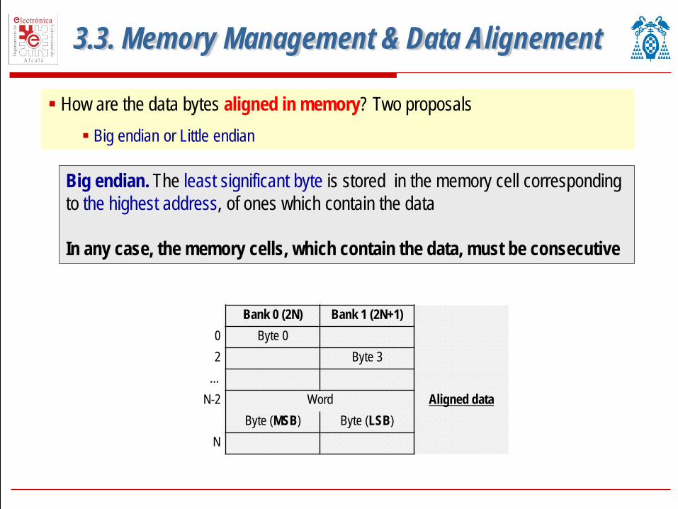
How are the data bytes aligned in memory? Two proposals Big endian or Little endian
Big endian. The least significant byte is stored in the memory cell corresponding to the highest address, of ones which contain the data In any case, the memory cells, which contain the data, must be consecutive
Bank 0 (2N) Bank 1 (2N+1) 0 Byte 0 2 Byte 3
… N-2 Word Aligned data
Byte (MSB) Byte (LSB) N
3.3. Memory Management & Data Alignement
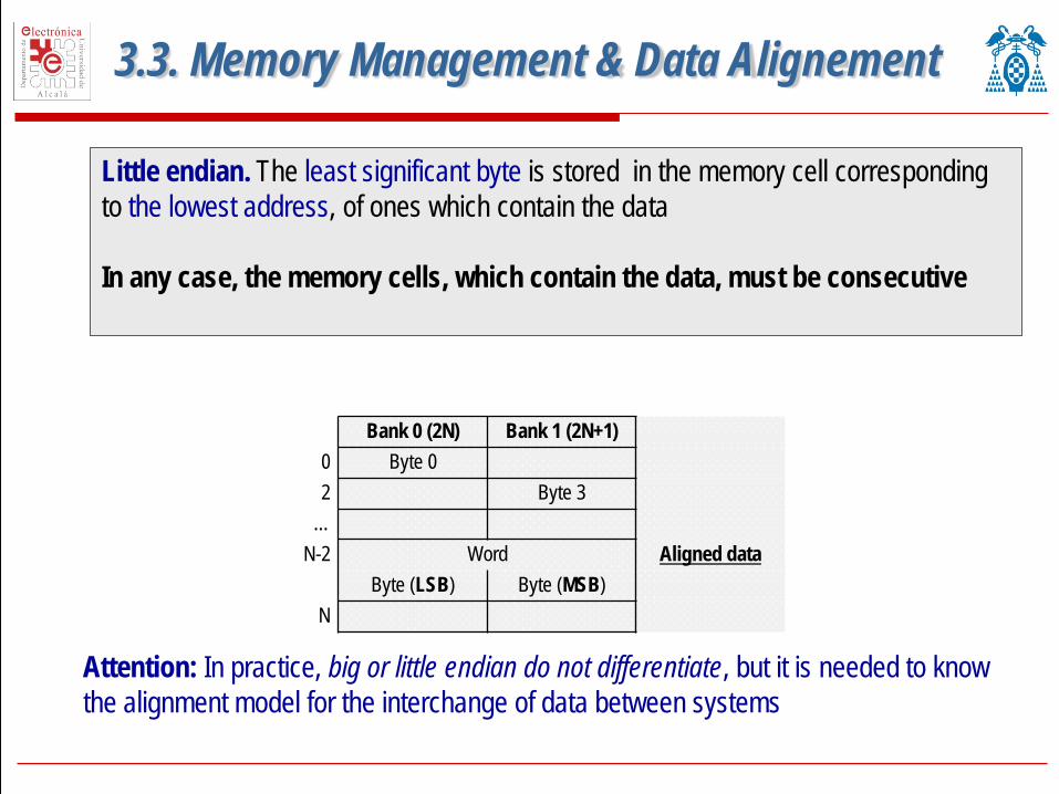
Little endian. The least significant byte is stored in the memory cell corresponding to the lowest address, of ones which contain the data In any case, the memory cells, which contain the data, must be consecutive
Attention: In practice, big or little endian do not differentiate, but it is needed to know the alignment model for the interchange of data between systems
Bank 0 (2N) Bank 1 (2N+1) 0 Byte 0 2 Byte 3
… N-2 Word Aligned data
Byte (LSB) Byte (MSB) N
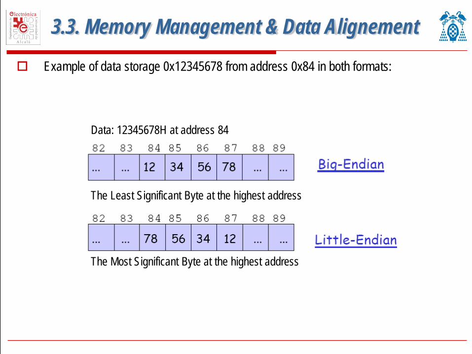
3.3. Memory Management & Data Alignement Example of data storage 0x12345678 from address 0x84 in both formats:
Data: 12345678H at address 84
The Least Significant Byte at the highest address
The Most Significant Byte at the highest address
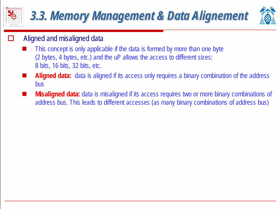
3.3. Memory Management & Data Alignement Aligned and misaligned data
This concept is only applicable if the data is formed by more than one byte (2 bytes, 4 bytes, etc.) and the uP allows the access to different sizes: 8 bits, 16 bits, 32 bits, etc.
Aligned data: data is aligned if its access only requires a binary combination of the address bus
Misaligned data: data is misaligned if its access requires two or more binary combinations of address bus. This leads to different accesses (as many binary combinations of address bus)
3.3. Memory Management & Data Alignement
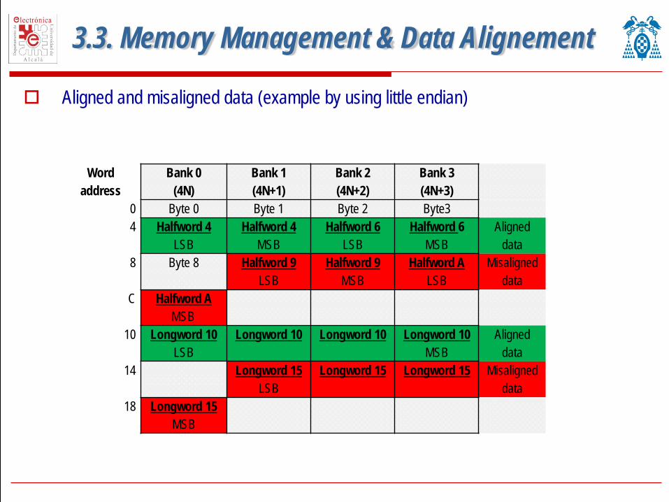
Aligned and misaligned data (example by using little endian)
Word address
Bank 0 (4N)
Bank 1 (4N+1)
Bank 2 (4N+2)
Bank 3 (4N+3)
0 Byte 0 Byte 1 Byte 2 Byte3 4 Halfword 4
LSB Halfword 4
MSB Halfword 6
LSB Halfword 6
MSB Aligned
data 8 Byte 8 Halfword 9
LSB Halfword 9
MSB Halfword A
LSB Misaligned
data C Halfword A
MSB
10 Longword 10 LSB
Longword 10
Longword 10
Longword 10 MSB
Aligned data
14 Longword 15 LSB
Longword 15
Longword 15
Misaligned data
18 Longword 15 MSB
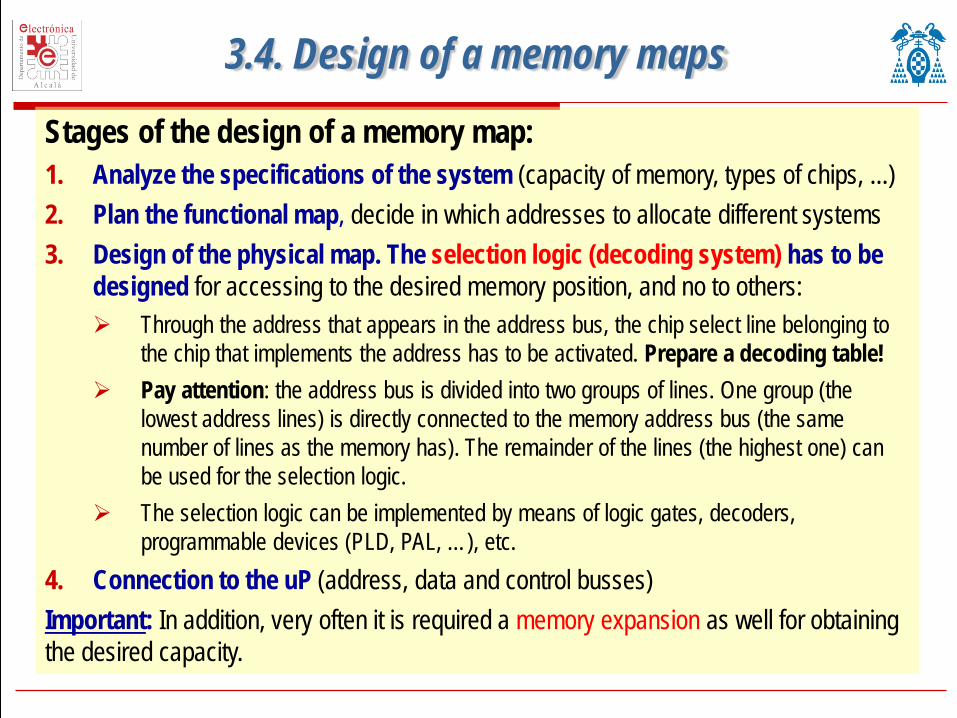
3.4. Design of a memory maps Stages of the design of a memory map: 1. Analyze the specifications of the system (capacity of memory, types of chips, ...) 2. Plan the functional map, decide in which addresses to allocate different systems 3. Design of the physical map. The selection logic (decoding system) has to be
designed for accessing to the desired memory position, and no to others: Through the address that appears in the address bus, the chip select line belonging to
the chip that implements the address has to be activated. Prepare a decoding table! Pay attention: the address bus is divided into two groups of lines. One group (the
lowest address lines) is directly connected to the memory address bus (the same number of lines as the memory has). The remainder of the lines (the highest one) can be used for the selection logic.
The selection logic can be implemented by means of logic gates, decoders, programmable devices (PLD, PAL, …), etc.
4. Connection to the uP (address, data and control busses) Important: In addition, very often it is required a memory expansion as well for obtaining the desired capacity.
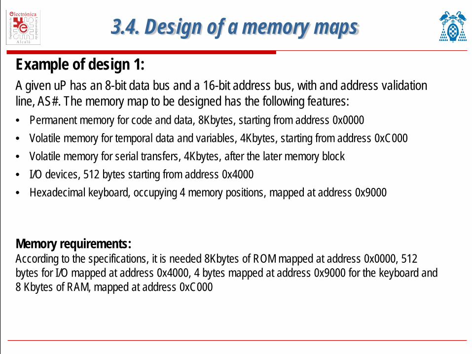
3.4. Design of a memory maps Example of design 1: A given uP has an 8-bit data bus and a 16-bit address bus, with and address validation line, AS#. The memory map to be designed has the following features: • Permanent memory for code and data, 8Kbytes, starting from address 0x0000 • Volatile memory for temporal data and variables, 4Kbytes, starting from address 0xC000 • Volatile memory for serial transfers, 4Kbytes, after the later memory block • I/O devices, 512 bytes starting from address 0x4000 • Hexadecimal keyboard, occupying 4 memory positions, mapped at address 0x9000 Memory requirements: According to the specifications, it is needed 8Kbytes of ROM mapped at address 0x0000, 512 bytes for I/O mapped at address 0x4000, 4 bytes mapped at address 0x9000 for the keyboard and 8 Kbytes of RAM, mapped at address 0xC000
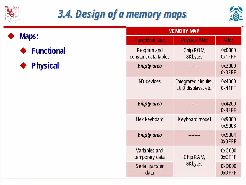
3.4. Design of a memory maps
Maps:
Functional
Physical
MEMORY MAP Functional Map Physical Map Addr.
Program and constant data tables
Chip ROM, 8Kbytes
0x0000 0x1FFF
Empty area ----- 0x2000 0x3FFF
I/O devices Integrated circuits, LCD displays, etc.
0x4000 0x41FF
Empty area ------- 0x4200
0x8FFF Hex keyboard Keyboard model 0x9000
0x9003 Empty area -------- 0x9004
0xBFFF Variables and
temporary data
Chip RAM, 8Kbytes
0xC000 0xCFFF
Serial transfer data
0xD000 0xDFFF

3.4. Design of a memory maps
Design of the selection logic: Decoding table
MEM. Data Bus
D[n-1:0]
A[12:0]
R/W# CS# OE#
Pay attention: the address base has to be a multiple of the block size (It has to finish in so many zeros “…000” as address lines has the chip)
Consider the base address Identify the function of the different address bits
Which bits are used for accessing to one position of the device?
Which bits are used for the selection logic?
Example: • For the RAM of 8 Kbytes and the ROM of 8 Kbytes, the address lines A[12..0] are
needed for selecting the desired memory position in the chip (for accessing to the block), so, they can have any value, thus it is represented by “XX...X”
• The remainder lines A[13..13], have a different value depending on the chip. This is: • “0 0 0” for ROM→ 0x0000 - 0x1FFF • “1 1 0” for RAM → 0xC000 - 0xDFFF
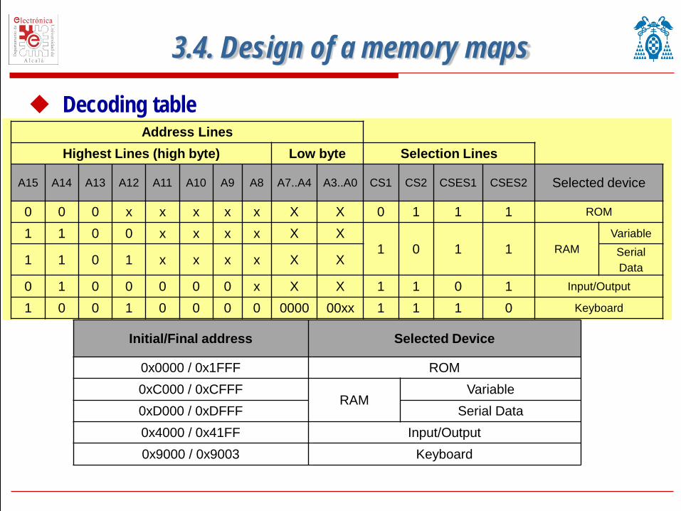
3.4. Design of a memory maps
Decoding table Address Lines
Highest Lines (high byte) Low byte Selection Lines
A15 A14 A13 A12 A11 A10 A9 A8 A7..A4 A3..A0 CS1 CS2 CSES1 CSES2 Selected device
0 0 0 x x x x x X X 0 1 1 1 ROM
1 1 0 0 x x x x X X 1 0 1 1 RAM
Variable
1 1 0 1 x x x x X X Serial Data
0 1 0 0 0 0 0 x X X 1 1 0 1 Input/Output
1 0 0 1 0 0 0 0 0000 00xx 1 1 1 0 Keyboard
Initial/Final address Selected Device
0x0000 / 0x1FFF ROM
0xC000 / 0xCFFF RAM
Variable
0xD000 / 0xDFFF Serial Data
0x4000 / 0x41FF Input/Output 0x9000 / 0x9003 Keyboard
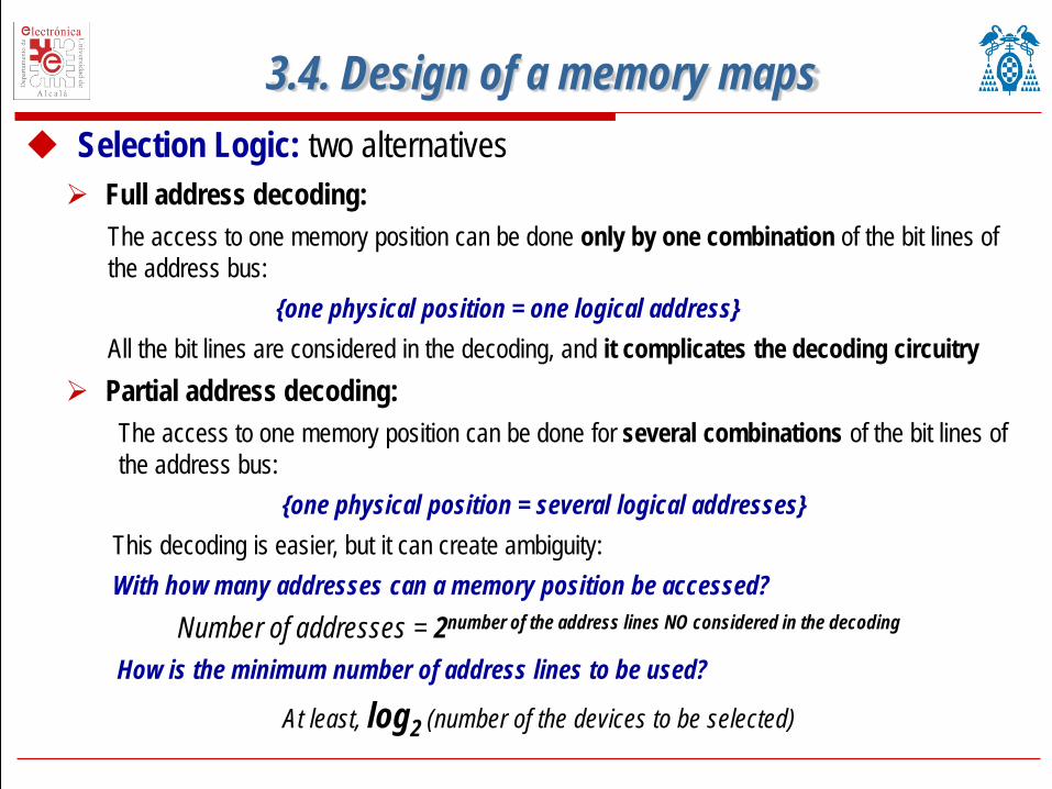
Full address decoding:
The access to one memory position can be done only by one combination of the bit lines of the address bus: {one physical position = one logical address}
All the bit lines are considered in the decoding, and it complicates the decoding circuitry Partial address decoding:
The access to one memory position can be done for several combinations of the bit lines of the address bus:
{one physical position = several logical addresses} This decoding is easier, but it can create ambiguity: With how many addresses can a memory position be accessed?
Number of addresses = 2number of the address lines NO considered in the decoding How is the minimum number of address lines to be used?
At least, log2 (number of the devices to be selected)
3.4. Design of a memory maps Selection Logic: two alternatives
3.4. Design of a memory maps
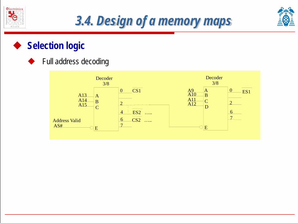
Selection logic Full address decoding
A B C
A13 A14 A15
0
2
4
CS1
CS2 …..
ES1
Decoder 3/8
E Address Valid AS# 7
B C D
A10 A11 A12
0
2
6
Decoder 3/8
E
7 6 ES2 …..
A9 A
3.4. Design of a memory maps
Design the selection logic belonging to the previous example by using partial address decoding
How many addresses are used for accessing to each device?
Exercise
3.4. Design of a memory maps
Example of design 2: A system has a space address of 64 K x 8, occupied for 2 Kbytes of memory ROM starting from address 0, and other 2 Kbytes of RAM starting from address 8000H. Besides, the 4 last addresses are used for selecting 4 registers belonging to a peripheral. Draw the address space and indicate the range address occupied for each device
Design the selection logic for full and partial address decoding
Example of design 2:
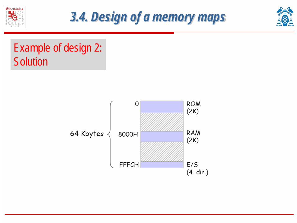
3.4. Design of a memory maps
Example of design 2: Solution
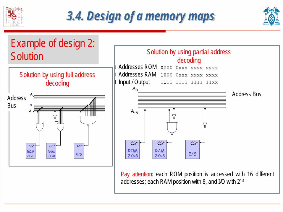
3.4. Design of a memory maps
Solution by using full address decoding
Solution by using partial address decoding
Pay attention: each ROM position is accessed with 16 different addresses; each RAM position with 8, and I/O with 213
Addresses ROM Addresses RAM Input / Output
Address Bus
Address Bus
Example of design 2: Solution

Access management and timing When analyzing uP connected to a memory device:
both uP + memory timings have to be studied and compared Access time to memory is a limiting factor of the performance of a
digital system Access time is always slow, compared with the uP Access time depends on memory type, technology and manufacturing It also depends on interconnection to the uP
Approach working with slow memories: Solution: extend the uP read/write cycle according to each memory
How? By adding wait cycles, until all data are read/written. How can wait cycles be added?
3.5. Access management and timing
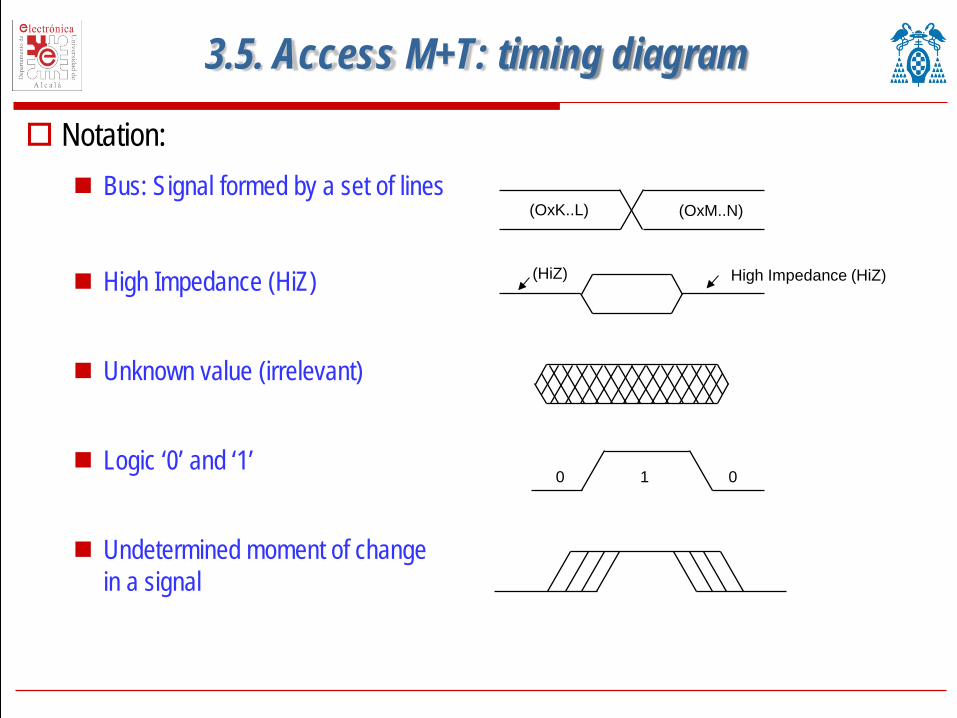
Notation: Bus: Signal formed by a set of lines
High Impedance (HiZ)
Unknown value (irrelevant)
Logic ‘0’ and ‘1’
Undetermined moment of change in a signal
0 0 1
High Impedance (HiZ) (HiZ)
(OxM..N) (OxK..L)
3.5. Access M+T: timing diagram

Access time (ttacc): from the transaction start (address valid at its bus) to the moment data is valid at its bus
Read cycle (tRC): minimum time between two consecutive accesses
tacc ≈ tRC
tacc
tRC
Data valid
Address valid Address Bus
CS
R/W
Data Bus
CPU
Memory
3.5. Access M+T: Read timing diagram

Write cycle (tWC): minimum time between two consecutive accesses
Writing pulse (tW): minimum time of write enable to perform the write
tWC Write cycle tW Writing pulse tDW Writing set-up time tDH Writing hold time tAW Writing address set-up time tWR Writing address hold time
Write cycle (tWC)
Data valid
Address valid Address Bus
CS
R/W
Data Bus
CPU tAW tWR
tDW tDH
tW
3.5. Access M+T: Write timing diagram
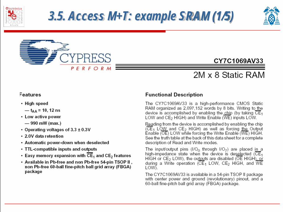
3.5. Access M+T: example SRAM (1/5)
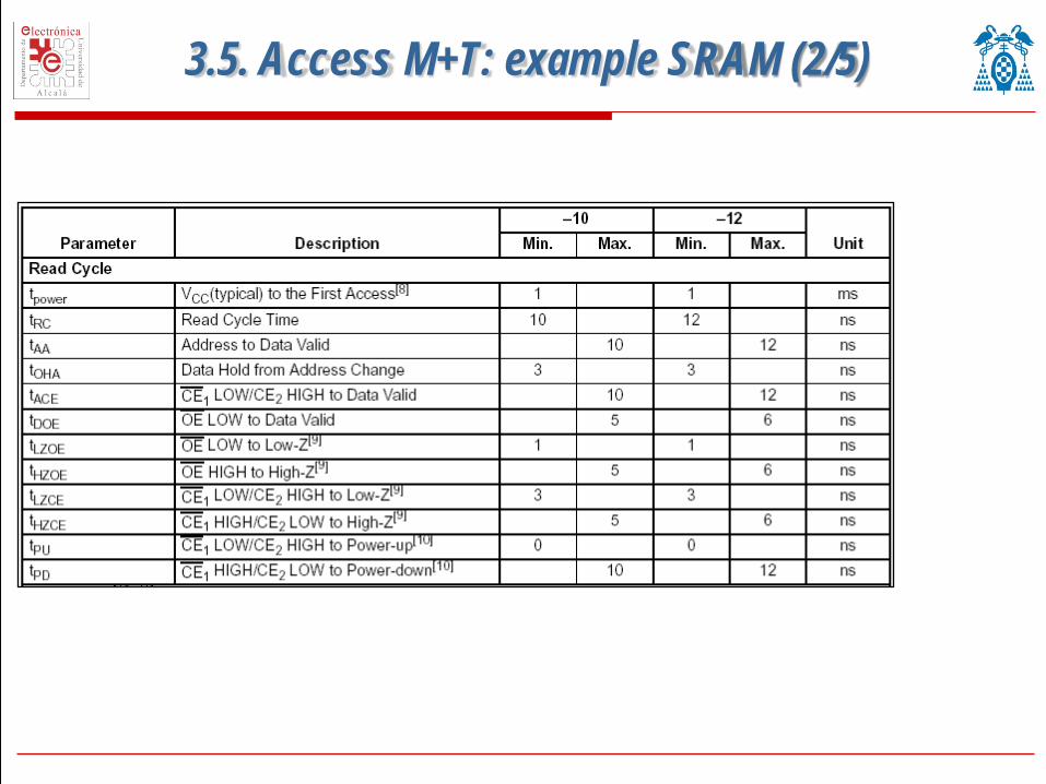
3.5. Access M+T: example SRAM (2/5)

3.5. Access M+T: example SRAM (3/5)
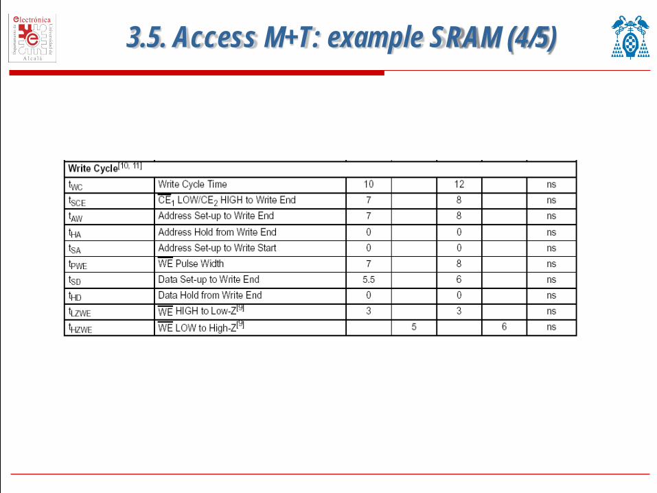
3.5. Access M+T: example SRAM (4/5)
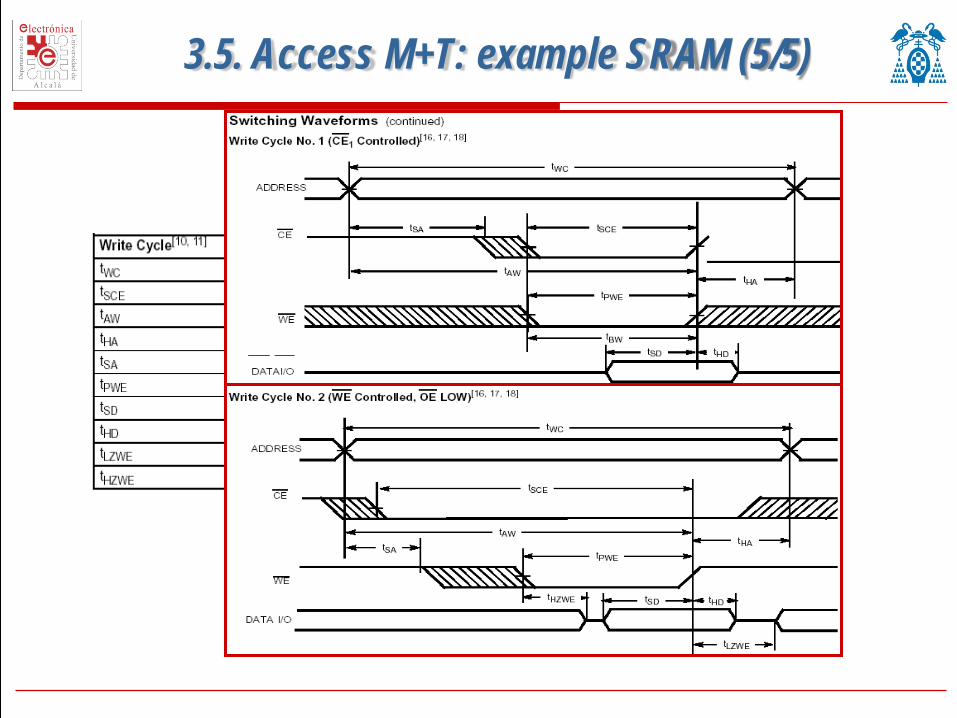
3.5. Access M+T: example SRAM (5/5)

3.5. Access M+T: example EPROM (1/5)
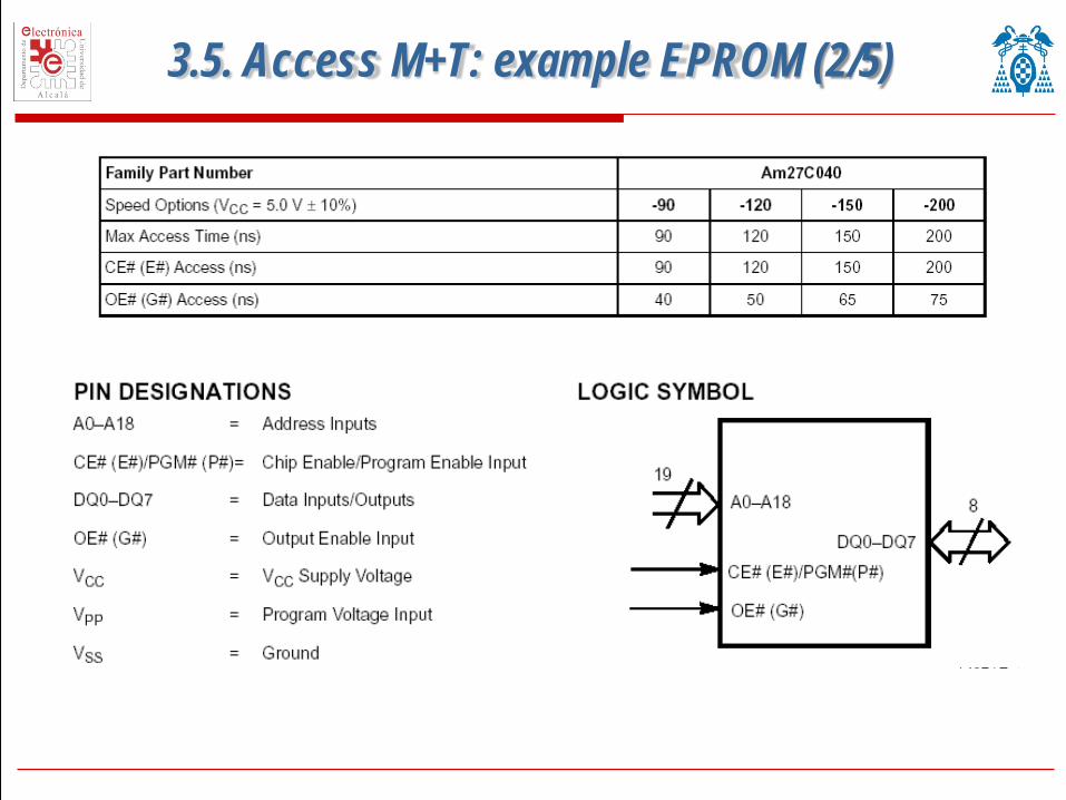
3.5. Access M+T: example EPROM (2/5)

3.5. Access M+T: example EPROM (3/5)

3.5. Access M+T: example EPROM (4/5)
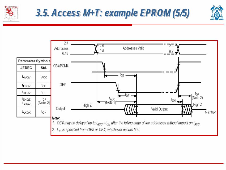
3.5. Access M+T: example EPROM (5/5)
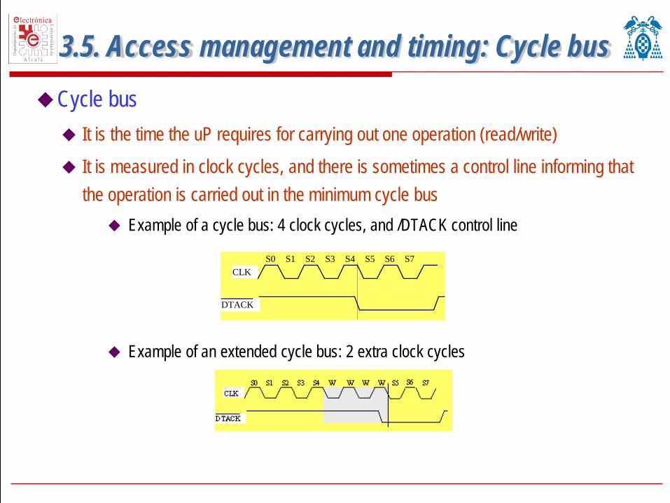
Cycle bus It is the time the uP requires for carrying out one operation (read/write) It is measured in clock cycles, and there is sometimes a control line informing that
the operation is carried out in the minimum cycle bus Example of a cycle bus: 4 clock cycles, and /DTACK control line
Example of an extended cycle bus: 2 extra clock cycles
3.5. Access management and timing: Cycle bus
DTACK
CLKS2S1S0 S4S3 S7S6S5
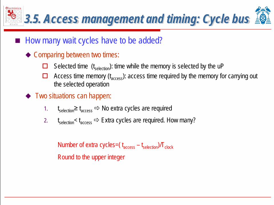
How many wait cycles have to be added? Comparing between two times:
Selected time (tselection): time while the memory is selected by the uP Access time memory (taccess): access time required by the memory for carrying out
the selected operation Two situations can happen:
1. tselection≥ taccess No extra cycles are required 2. tselection< taccess Extra cycles are required. How many?
Number of extra cycles=( taccess – tselection)/Tclock
Round to the upper integer
3.5. Access management and timing: Cycle bus
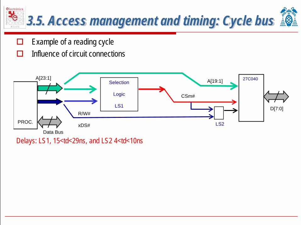
Example of a reading cycle Influence of circuit connections Delays: LS1, 15<td<29ns, and LS2 4<td<10ns
3.5. Access management and timing: Cycle bus
27C040
D[7:0]
A[19:1]
PROC.
Data Bus
A[23:1] Selection
Logic
LS1
CSm#
R/W#
xDS# LS2
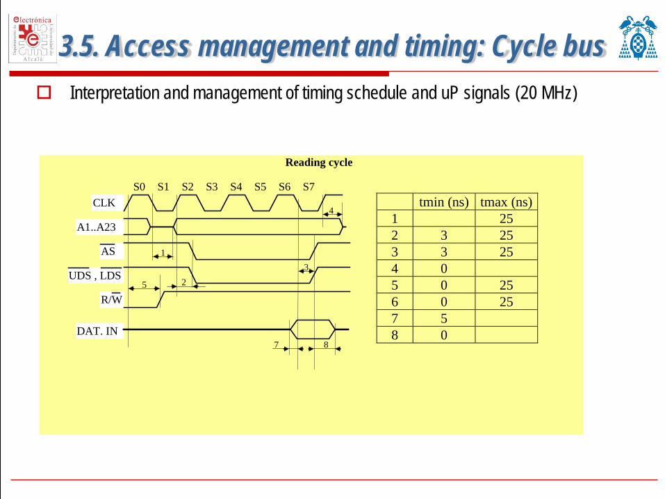
Interpretation and management of timing schedule and uP signals (20 MHz)
Reading cycle
DAT. IN
R/W
UDS , LDS
AS
A1..A23
CLK S2 S1 S0 S4 S3 S7 S6 S5
7 8
5 2
4
3 1
tmin (ns) tmax (ns) 1 25 2 3 25 3 3 25 4 0 5 0 25 6 0 25 7 5 8 0
3.5. Access management and timing: Cycle bus
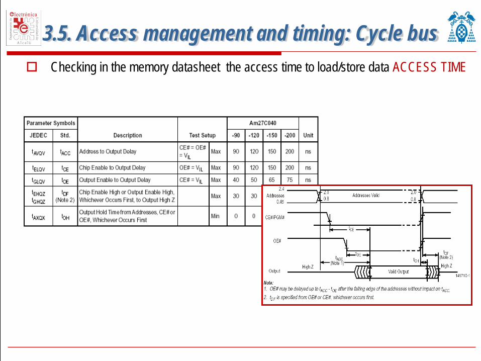
Checking in the memory datasheet the access time to load/store data ACCESS TIME
3.5. Access management and timing: Cycle bus

Digital Electronic Systems Department of Electronics
Generate a timing schedule where intermediate uP signals in the circuit and chip select memory signal are included
Compute the memory select time
3.5. Access management and timing: Cycle bus
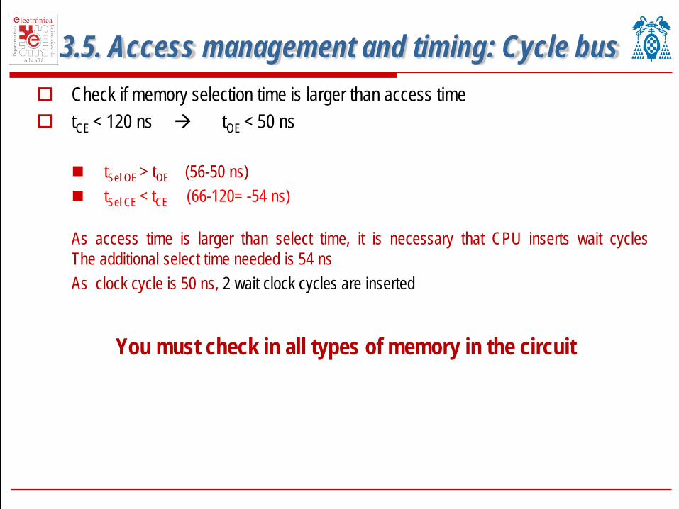
Check if memory selection time is larger than access time tCE < 120 ns tOE < 50 ns
tSel OE > tOE (56-50 ns) tSel CE < tCE (66-120= -54 ns)
As access time is larger than select time, it is necessary that CPU inserts wait cycles The additional select time needed is 54 ns As clock cycle is 50 ns, 2 wait clock cycles are inserted
You must check in all types of memory in the circuit
3.5. Access management and timing: Cycle bus