CNC Programming Lathe Axes Designation Lathe Lathe Axes Designation.

2 Axes Motor Control IC with High Functions
MCX512 User’s Manual
2016-08-22 Ver. 1.0 2017-01-17 Ver. 2.0
NOVA electronics

NOVA electronics Inc. MCX512 - i
- i -
1. OUTLINE ................................................................ 1 1.1 The Main Features of Functions ..................................................................................................... 1 1.2 Functional Block Diagram ............................................................................................................... 8 1.3 Specification Table ........................................................................................................................ 10
2. The Descriptions of Functions .............................. 14 2.1 Fixed Pulse Driving and Continuous Pulse Driving....................................................................... 14
2.1.1 Relative Position Driving ...................................................................................................................... 14 2.1.2 Absolute Position Driving ..................................................................................................................... 15 2.1.3 Counter Relative Position Driving ......................................................................................................... 15 2.1.4 Continuous Pulse Driving ..................................................................................................................... 17
2.2 Acceleration and Deceleration ...................................................................................................... 19 2.2.1 Constant Speed Driving ....................................................................................................................... 19 2.2.2 Trapezoidal Driving [Symmetrical] ........................................................................................................ 20 2.2.3 Non-Symmetrical Trapezoidal Acceleration .......................................................................................... 22 2.2.4 S-curve Acceleration/Deceleration Driving [Symmetrical] ..................................................................... 24 2.2.5 Non-symmetrical S-Curve Acceleration/Deceleration ........................................................................... 30 2.2.6 Pulse Width and Speed Accuracy ......................................................................................................... 32
2.3 Position Control ............................................................................................................................ 33 2.3.1 Logical Position Counter and Real position Counter ............................................................................. 33 2.3.2 Position Comparison ............................................................................................................................ 33 2.3.3 Software Limit ...................................................................................................................................... 33 2.3.4 Position Counter Variable Ring ............................................................................................................. 34
2.4 Multi-Purpose Register ................................................................................................................. 35 2.4.1 Comparative Object and Comparison Condition ................................................................................... 35 2.4.2 Usage of Comparison Result ................................................................................................................ 36 2.4.3 Load/Save of Parameters by Synchronous Action ................................................................................ 39
2.5 Automatic Home Search ............................................................................................................... 40 2.5.1 Operation of Each Step ........................................................................................................................ 41 2.5.2 Deviation Counter Clearing Signal Output ............................................................................................ 44 2.5.3 Timer Between Steps ........................................................................................................................... 44 2.5.4 Setting a Search Speed and a Mode .................................................................................................... 45 2.5.5 Execution of Automatic Home Search and the Status ........................................................................... 49 2.5.6 Errors Occurring at Automatic Home Search ........................................................................................ 50 2.5.7 Notes on Automatic Home Search ........................................................................................................ 51 2.5.8 Examples of Automatic Home Search .................................................................................................. 52
2.6 Synchronous Action ...................................................................................................................... 58 2.6.1 Activation Factor .................................................................................................................................. 60
NOVA electronics Inc. MCX512 - ii
- ii -
2.6.2 Action ................................................................................................................................................... 62 2.6.3 Synchronous Action Settings ................................................................................................................ 66 2.6.4 Synchronous Action Execution ............................................................................................................. 69 2.6.5 Interrupt by Synchronous Action ........................................................................................................... 69 2.6.6 Examples of Synchronous Action ......................................................................................................... 70 2.6.7 Synchronous Action Delay Time ........................................................................................................... 75
2.7 Split Pulse .................................................................................................................................... 77 2.7.1 Split Pulse Setting ................................................................................................................................ 77 2.7.2 Start/Termination of Split Pulse ............................................................................................................ 78 2.7.3 Split Pulse in Synchronous Action ........................................................................................................ 79 2.7.4 Interrupt by Split Pulse ......................................................................................................................... 79 2.7.5 Notes on Split Pulse ............................................................................................................................. 79 2.7.6 Examples of Split Pulse ........................................................................................................................ 80
2.8 General Purpose Input/Output Signal ........................................................................................... 86 2.8.1 nPIOm Signal ....................................................................................................................................... 86 2.8.2 Other Input Signals .............................................................................................................................. 89
2.9 Timer ............................................................................................................................................ 90 2.9.1 Timer Operation ................................................................................................................................... 90 2.9.2 Timer Setting ........................................................................................................................................ 91 2.9.3 Timer-Start/Timer-Stop ......................................................................................................................... 91 2.9.4 Timer and Synchronous Action ............................................................................................................. 91 2.9.5 Timer Operating State and Current Timer Value Reading ..................................................................... 91 2.9.6 Interrupt by Timer ................................................................................................................................. 91 2.9.7 Examples of Timer................................................................................................................................ 92
2.10 Interrupt ........................................................................................................................................ 95 2.10.1 Interrupt from X, Y axes........................................................................................................................ 95 2.10.2 Interrupt during Continuous Interpolation.............................................................................................. 96
2.11 Input Signal Filter ......................................................................................................................... 97 2.11.1 Setting of Input Signal Filter Function ................................................................................................... 98 2.11.2 Example of Setting Input Signal Filters ................................................................................................. 99
2.12 Other Functions .......................................................................................................................... 100 2.12.1 Driving By External Signals .................................................................................................................100 2.12.2 Pulse Output Type Selection ...............................................................................................................103 2.12.3 Encoder Pulse Input Type Selection ....................................................................................................104 2.12.4 Hardware Limit Signals .......................................................................................................................105 2.12.5 Interface to Servo Motor Driver ...........................................................................................................106 2.12.6 Emergency Stop ..................................................................................................................................106 2.12.7 Status Output ......................................................................................................................................107

NOVA electronics Inc. MCX512 - iii
- iii -
3. Interpolation ....................................................... 108 3.1 2-axis Linear Interpolation ........................................................................................................... 111
3.1.1 Maximum Finish Point ......................................................................................................................... 111 3.1.2 Examples of Linear Interpolation for 2 axes ......................................................................................... 112
3.2 Circular Interpolation ................................................................................................................... 113 3.2.1 The Finish Point Checking of Circular Interpolation ............................................................................. 114 3.2.2 Toggle of Interpolation Axis ................................................................................................................. 114 3.2.3 The Example for CW Circular Interpolation.......................................................................................... 114
3.3 2 axes Bit Pattern Interpolation ................................................................................................... 115 3.3.1 Set Interpolation Axis Valid .................................................................................................................. 116 3.3.2 Interpolation Speed Setting ................................................................................................................. 116 3.3.3 Bit Pattern Data Writing ....................................................................................................................... 116 3.3.4 Write of Interpolation Driving Command .............................................................................................. 117 3.3.5 Termination of Interpolation ................................................................................................................. 117 3.3.6 Check Available Space of Pre-buffer ................................................................................................... 118 3.3.7 Interruption of Interpolation Driving ..................................................................................................... 118 3.3.8 Example of Bit Pattern Interpolation .................................................................................................... 119
3.4 Constant Vector Speed ............................................................................................................... 120 3.4.1 Constant Vector Speed Setting............................................................................................................121
3.5 Short Axis Pulse Equalization ..................................................................................................... 122 3.5.1 Short Axis Pulse Equalization Setting ..................................................................................................122 3.5.2 Notes on Using Short Axis Pulse Equalization .....................................................................................123
3.6 Continuous Interpolation ............................................................................................................. 124 3.6.1 How to Perform Continuous Interpolation ............................................................................................125 3.6.2 Continuous Interpolation by Using Interrupt .........................................................................................127 3.6.3 Errors during Continuous Interpolation ................................................................................................128 3.6.4 Attention for Continuous Interpolation .................................................................................................128 3.6.5 Example of Continuous Interpolation ...................................................................................................129
3.7 Acceleration/Deceleration Control in Interpolation ...................................................................... 131 3.7.1 Acceleration/Deceleration for 2-axis Linear Interpolation .....................................................................131 3.7.2 Acceleration/Deceleration for Circular Interpolation and Bit Pattern Interpolation ................................131 3.7.3 Acceleration/Deceleration for Continuous Interpolation .......................................................................133
3.8 Single-step interpolation ............................................................................................................. 134 3.8.1 Command Controlled Single-step Interpolation ...................................................................................134 3.8.2 Attention for Single-step Interpolation..................................................................................................134
4. I2C Serial Bus ..................................................... 135 4.1 Pins used in I2C Bus Mode ......................................................................................................... 135
4.1.1 Pull-up Resistor (Rp) ...........................................................................................................................135
NOVA electronics Inc. MCX512 - iv
- iv -
4.1.2 I2CRSTN Reset...................................................................................................................................136 4.2 I2C Bus Transmitting and Receiving ........................................................................................... 136
4.2.1 Writing Operation ................................................................................................................................137 4.2.2 Reading Operation ..............................................................................................................................138 4.2.3 Notes on Using I2C Serial Bus .............................................................................................................140 4.2.4 Connection Example ...........................................................................................................................140 4.2.5 Control Example ..................................................................................................................................141
5. Pin Assignments and Signal Description ............ 144 5.1 Pin Assignments ......................................................................................................................... 144 5.2 Signal Description....................................................................................................................... 145 5.3 Input/Output Logic ...................................................................................................................... 150 5.4 Remarks of Logic Design ........................................................................................................... 151
6. Register .............................................................. 152 6.1 Register Address by 16-bit Data Bus .......................................................................................... 152 6.2 Register Address by 8-bit Data Bus ............................................................................................ 154 6.3 Register Address by I2C Serial Interface Bus Mode ................................................................... 154 6.4 Command Register: WR0 ........................................................................................................... 155 6.5 Mode Register1: WR1 ................................................................................................................ 155 6.6 Mode Register2: WR2 ................................................................................................................ 156 6.7 Mode Register3: WR3 ................................................................................................................ 157 6.8 Output Register: WR4 ................................................................................................................ 159 6.9 Output Register: WR5 ................................................................................................................ 159 6.10 Data Register: WR6/WR7 ........................................................................................................... 160 6.11 Main Status Register: RR0 ......................................................................................................... 161 6.12 Status Register 1: RR1 ............................................................................................................... 162 6.13 Status Register 2: RR2 ............................................................................................................... 163 6.14 Status Register 3: RR3 ............................................................................................................... 164 6.15 PIO Read Register 1: RR4 ......................................................................................................... 166 6.16 PIO Read Register 2: RR5 ......................................................................................................... 166 6.17 Data-Read Register: RR6/RR7 ................................................................................................... 166
7. Commands ......................................................... 167 7.1 Command Lists ........................................................................................................................... 167 7.2 Commands for Writing Data ....................................................................................................... 171
7.2.1 Jerk Setting .........................................................................................................................................171 7.2.2 Deceleration Increasing Rate Setting ..................................................................................................171 7.2.3 Acceleration Setting ............................................................................................................................172 7.2.4 Deceleration Setting ............................................................................................................................172

NOVA electronics Inc. MCX512 - v
- v -
7.2.5 Initial Speed Setting ............................................................................................................................173 7.2.6 Drive Speed Setting ............................................................................................................................173 7.2.7 Drive pulse number / Finish point setting .............................................................................................174 7.2.8 Manual Decelerating Point Setting ......................................................................................................174 7.2.9 Circular Center Point Setting ...............................................................................................................175 7.2.10 Logical Position Counter Setting .........................................................................................................175 7.2.11 Real Position Counter Setting .............................................................................................................175 7.2.12 Software Limit + Setting ......................................................................................................................175 7.2.13 Software Limit − Setting ......................................................................................................................176 7.2.14 Acceleration Counter Offsetting ...........................................................................................................176 7.2.15 Logical Position Counter Maximum Value Setting ................................................................................176 7.2.16 Real Position Counter Maximum Value Setting ....................................................................................176 7.2.17 Multi-Purpose Register 0 Setting .........................................................................................................177 7.2.18 Multi-Purpose Register 1 Setting .........................................................................................................177 7.2.19 Multi-Purpose Register 2 Setting .........................................................................................................177 7.2.20 Multi-Purpose Register 3 Setting .........................................................................................................178 7.2.21 Home Search Speed Setting ...............................................................................................................178 7.2.22 Speed Increasing/Decreasing Value Setting ........................................................................................178 7.2.23 Timer Value Setting .............................................................................................................................179 7.2.24 Split Pulse Setting 1 ............................................................................................................................179 7.2.25 Split Pulse Setting 2 ............................................................................................................................179 7.2.26 Interpolation/Finish Point Maximum Value Setting ...............................................................................180
7.3 Commands for Writing Mode ...................................................................................................... 181 7.3.1 Multi-Purpose Register Mode Setting ..................................................................................................181 7.3.2 PIO Signal Setting 1 ............................................................................................................................182 7.3.3 PIO Signal Setting 2・Other Settings ..................................................................................................184 7.3.4 Automatic Home Search Mode Setting 1 .............................................................................................185 7.3.5 Automatic Home Search Mode Setting 2 .............................................................................................186 7.3.6 Input Signal Filter Mode Setting ..........................................................................................................188 7.3.7 Synchronous Action SYNC0, 1, 2, 3 Setting ........................................................................................189 7.3.8 Interpolation Mode Setting ..................................................................................................................191 7.3.9 PIO Signal Setting 3 ............................................................................................................................192
7.4 Commands for Reading Data ..................................................................................................... 193 7.4.1 Logical Position Counter Reading .......................................................................................................193 7.4.2 Real Position Counter Reading ...........................................................................................................193 7.4.3 Current Drive Speed Reading..............................................................................................................193 7.4.4 Current Acceleration/Deceleration Reading .........................................................................................194 7.4.5 Multi-Purpose Register 0 Reading .......................................................................................................194 7.4.6 Multi-Purpose Register 1 Reading .......................................................................................................194

NOVA electronics Inc. MCX512 - vi
- vi -
7.4.7 Multi-Purpose Register 2 Reading .......................................................................................................194 7.4.8 Multi-Purpose Register 3 Reading .......................................................................................................195 7.4.9 Current Timer Value Reading ..............................................................................................................195 7.4.10 Interpolation/Finish point maximum value Reading ..............................................................................195 7.4.11 WR1 Setting Value Reading ................................................................................................................195 7.4.12 WR2 Setting Value Reading ................................................................................................................196 7.4.13 WR3 Setting Value Reading ................................................................................................................196 7.4.14 Multi-Purpose Register Mode Setting Reading ....................................................................................196 7.4.15 PIO Signal Setting 1 Reading ..............................................................................................................196 7.4.16 PIO Signal Setting 2/Other Settings Reading ......................................................................................197 7.4.17 Acceleration Setting Value Reading.....................................................................................................197 7.4.18 Initial Speed Setting Value Reading ....................................................................................................197 7.4.19 Drive Speed Setting Value Reading .....................................................................................................197 7.4.20 Drive Pulse Number/Finish Point Setting Value Reading .....................................................................198 7.4.21 Split Pulse Setting 1 Reading ..............................................................................................................198 7.4.22 General Purpose Input Value Reading ................................................................................................198 7.4.23 PIO Signal Setting 3 ............................................................................................................................198
7.5 Driving Commands ..................................................................................................................... 199 7.5.1 Relative Position Driving .....................................................................................................................199 7.5.2 Counter Relative Position Driving ........................................................................................................200 7.5.3 + Direction Continuous Pulse Driving ..................................................................................................200 7.5.4 − Direction Continuous Pulse Driving ..................................................................................................200 7.5.5 Absolute Position Driving ....................................................................................................................201 7.5.6 Decelerating Stop ................................................................................................................................201 7.5.7 Instant Stop .........................................................................................................................................201 7.5.8 Direction Signal + Setting ....................................................................................................................201 7.5.9 Direction Signal - Setting .....................................................................................................................202 7.5.10 Automatic Home Search Execution .....................................................................................................202
7.6 Interpolation Commands............................................................................................................. 203 7.6.1 2-axis Linear Interpolation Driving .......................................................................................................203 7.6.2 CW Circular Interpolation Driving ........................................................................................................203 7.6.3 CCW Circular Interpolation Driving ......................................................................................................203 7.6.4 2-Axis Bit Pattern Interpolation Driving ................................................................................................204 7.6.5 Deceleration Enabling .........................................................................................................................204 7.6.6 Deceleration Disabling ........................................................................................................................204 7.6.7 Interpolation Interrupt Clear/Single-step Interpolation ..........................................................................204
7.7 Synchronous Action Operation Commands ................................................................................ 205 7.7.1 Synchronous Action Enable Setting .....................................................................................................205 7.7.2 Synchronous Action Disable Setting ....................................................................................................206

NOVA electronics Inc. MCX512 - vii
- vii -
7.7.3 Synchronous Action Activation ............................................................................................................206 7.8 Other Commands ....................................................................................................................... 207
7.8.1 Speed Increase ...................................................................................................................................207 7.8.2 Speed Decrease..................................................................................................................................207 7.8.3 Deviation Counter Clear Output...........................................................................................................208 7.8.4 Timer-Start ..........................................................................................................................................208 7.8.5 Timer-Stop ..........................................................................................................................................208 7.8.6 Start of Split Pulse ...............................................................................................................................208 7.8.7 Termination of Split Pulse ....................................................................................................................209 7.8.8 Drive Start Holding ..............................................................................................................................209 7.8.9 Drive Start Holding Release ................................................................................................................209 7.8.10 Error/Finishing Status Clear ................................................................................................................209 7.8.11 RR3 Page 0 Display ............................................................................................................................210 7.8.12 RR3 Page 1 Display ............................................................................................................................210 7.8.13 Maximum finish point clear ..................................................................................................................210 7.8.14 NOP ....................................................................................................................................................210 7.8.15 Command Reset ................................................................................................................................. 211
8. Connection Examples ........................................ 212 8.1 Example of 16-bit Bus Mode Connection ................................................................................... 212 8.2 Example of Connection in I2C Bus Mode ................................................................................. 213 8.3 Connection Example .................................................................................................................. 214 8.4 Pulse Output Interface ................................................................................................................ 214 8.5 Connection Example for Input Signals ........................................................................................ 215 8.6 Connection Example for Encoder ............................................................................................... 215
9. Example Program ............................................... 216
10. Electrical Characteristics ................................. 228 10.1 DC Characteristics ...................................................................................................................... 228 10.2 AC Characteristics ...................................................................................................................... 229
10.2.1 Clock ...................................................................................................................................................229 10.2.2 Read/Write Cycle ................................................................................................................................229 10.2.3 CLK/Output Signal Timing ...................................................................................................................230 10.2.4 Input Pulses ........................................................................................................................................230 10.2.5 General Purpose Input/Output Signals (nPIO13~0) .............................................................................231 10.2.6 Split Pulse ...........................................................................................................................................231 10.2.7 I2C Serial Bus (At fast mode.) ..............................................................................................................232
11. Timing of Input/Output Signals ........................ 233 11.1 Power-On Reset ......................................................................................................................... 233
NOVA electronics Inc. MCX512 - viii
- viii -
11.2 Timing of drive start/finish ........................................................................................................... 233 11.3 Interpolation Driving ................................................................................................................... 234 11.4 Start Driving after Hold Command .............................................................................................. 234 11.5 Instant Stop ................................................................................................................................ 234 11.6 Decelerating Stop ....................................................................................................................... 235 11.7 Detailed Timing of Split Pulse ..................................................................................................... 235
12. Package Dimensions ...................................... 236
13. Storage and Recommended Installation Conditions ............................................................. 237
13.1 Storage of this IC ........................................................................................................................ 237 13.2 Standard Installation Conditions by Soldering Iron ..................................................................... 237 13.3 Standard Installation Conditions by Solder Reflow ..................................................................... 237
Appendix A Calculation Formula of Acceleration/Deceleration Drive ............................ A-1
A-1 Case of Trapezoidal Acceleration/Deceleration Driving ............................................................... A-1 A-2 Case of S-curve Acceleration/Deceleration Driving ..................................................................... A-2
Appendix B Parameter Calculation Formula when Input Clock except 16MHz..................................... B-1
Appendix C Differences with MCX300 series ...... 13-1

NOVA electronics Inc. MCX512 - ix
- ix -
Revision History
1st edition 2016-10-07 Newly created. 2nd edition 2017-01-17 2.2.3 Non-Symmetrical Trapezoidal Acceleration
Delete the description about speed changing. Add [after checking the interpolation drive stops] when writing error/finishing status clear command (79h) into the interpolation axis with to the following chapters. 2.6.2 Action 3.Interpolation 3.6.3 Errors during Continuous Interpolation 3.6.4 Attention for Continuous Interpolation 6.11 RR0 6.13 RR2 7.8.10 Error/Finishing Status Clear Appendix C Modify the description about the example in the manual Add the speed changing during interpolation drive with the following chapters 3.Inteprolation 3.6.4 Attention for Continuous Interpolation 7.2.6 Drive Speed Setting 5.2 Signal Description : Modify the descriptions of EXPP 10.1 DC Characteristics : Modify the symbol of Operating Temperature

NOVA electronics Inc. MCX512 - x
- x -
Introduction In general, semiconductor products sometimes malfunction or fail to function. When incorporating this IC in a system, make sure that a safe system is designed to avoid any injuries or property damage caused by malfunctioning of this IC. This IC is designed for application in general electronic devices (industrial automation devices, industrial robots, measuring instruments, computers, office equipment, household electrical goods, and so on). This IC is not intended for the use in high-performance and high-reliability equipment whose failure or malfunctioning may directly cause death or injuries (atomic energy control equipment, aerospace equipment, transportation equipment, medical equipment, and various safety devices) and the operation for such use is not guaranteed. The customer shall be responsible for the use of this IC in any such high-performance and high-reliability equipment. “Japanese Foreign Exchange and Foreign Trade Act” and other export-related laws and regulations must be observed and complied with. Do not use this IC for the purpose of the development of weapons such as mass destruction weapons and any military purposes. This IC shall not be used in equipment that manufacture, use and sale are prohibited by domestic and foreign laws and regulations. Information in this manual is subject to change without notice for continuous improvement in the product. You can download the latest manual and software from our web site: http://www.novaelec.co.jp/eng Please also feel free to contact us directly for any inquiries or questions. Operating Precautions Before using the MCX512, please read this manual thoroughly to ensure correct usage within the scope of the specification such as the signal voltage, signal timing, and operation parameter values. Operation is not verified in all combinations of modes and parameters. The user should fully verify and evaluate the operation with a combination of the mode and parameter that is used before using this IC. Treatment of unused pins that are not pulled up in the IC Make sure that unused input pins are connected to GND or VDD. If these pins are open, the signal level of pins will unstable and may cause malfunction. Make sure that unused bi-directional pins are connected to VDD or GND through high impedance (about 10k~ 100 kΩ). If these pins are directly connected to GND or VDD, the IC may be damaged by overcurrent in case of such as a programming mistake causes the output state. About Reset Make sure to reset the IC when the power is on. This IC will be reset if RESETN signal is set to Low for more than 8 CLK cycles when a stable clock has been input. Please note that the IC will not be reset if the clock is not input. Note on S-curve Acceleration/Deceleration Driving This IC is equipped with a function that performs decelerating stop for fixed pulse driving in S-curve deceleration with the symmetrical acceleration/deceleration. However, when the initial speed is set to an extremely low speed, slight premature termination or creep may occur. Before using S-curve deceleration driving, make sure that your system allows premature termination or creep.

NOVA electronics Inc. MCX512 - xi
- xi -
Terms and Symbols used in the Manual Active The function of a signal is the state of being enabled. Drive Action to output pulses for rotating a motor to the driver (drive unit) of a pulse type servo motor
or stepping motor. Fixed pulse drive Drive that outputs specified pulses. Three types of drives: relative position drive, counter
relative position drive and absolute position drive are available. Continuous pulse drive Drive that outputs pulses up to infinity unless a stop factor becomes active. CW Clockwise direction (abbreviation of clockwise) CCW Counter-clockwise direction (abbreviation of counter-clockwise) Interpolation segment Each interpolation driving that comprises continuous interpolation. Jerk Acceleration increasing/decreasing rate per unit time. This term includes a decreasing rate of
acceleration (=Jerk). Deceleration increasing rate Deceleration increasing/decreasing rate per unit time. This term includes a decreasing rate of
deceleration. 2's complement 2's complement is used to represent negative numbers in binary.
[Example] In 16-bit length, -1 is FFFFh, -2 is FFFEh, -3 is FFFDh, … -32768 is 8000h. Creep In deceleration of acceleration/ deceleration fixed pulse driving, output of specified driving
pulses is not completed even if the speed reaches the initial speed and the rest of driving pulses is output at the initial speed (= Creep).
Premature termination In deceleration of acceleration/ deceleration fixed pulse driving, output of specified driving
pulses is completed and driving is terminated before the speed reaches the initial speed. This is a reverse behavior of creep.
↑ The rising edge of when a signal changes its level from Low to Hi. ↓ The falling edge of when a signal changes its level from Hi to Low. n The signal name of each axis X, Y, Z and U is written as n. This “n” stands for X, Y, Z or
U. nPIOm PIO signal of each axis X, Y, Z and U is written as nPIOm. This “n” stands for X, Y, Z or U, and
“m” stands for 0~7 of PIO0~PIO7. SYNCm Synchronous action set SYNC0~SYNC3 is written as SYNCm. This “m” stands for 0~3 of
SYNC0~SYNC3. MRm Multi-purpose register MR0~MR3 is written as MRm. This “m” stands for 0~3 of MR0~MR3.

NOVA electronics Inc. MCX512 - 1
- 1 -
1. OUTLINE
1.1 The Main Features of Functions
MCX512 is 2-axis motion control IC from MCX500 series of which functions are drastically improved from MCX300 series.
For interpolation function, 8 stages of pre-buffer to continuously execute linear and circular interpolation is equipped. This enables us to execute more slight continuous interpolation. In addition to this, constant vector speed mode, short axis pulse equalization mode for continuous interpolation and so on are available. MCX500 series motion control IC has no multiple of speed (speed range-free). This enables us to freely set and vary the drive speed linearly from 1 pps up to 8 Mpps in increments of 1pps without changing the range. MCX512 can be connected to a host CPU with either 8-bit or 16-bit bus, and I2C serial interface bus. It can also be connected to a CPU without a parallel bus.
8 Stages of Pre-Buffer for Continuous Interpolation
MCX512 is equipped with 8 stages of pre-buffer register that stores finish point data (and others) in each segment, in order to handle continuous interpolation driving at high-speed. In the case of the previous MCX300 having only 1 stage of pre-buffer, when performing continuous interpolation, driving time of each interpolation segment must be longer than setting time of position data for next segment. Therefore, minimum drive pulses of each segment are restricted depending on interpolation drive speed. For instance, when setting time of data to CPU is TDS=80μsec and interpolation drive speed is V=100Kpps, minimum drive pulses are required at least 8 pulses or more MCX512 increases pre-buffer to 8 stages and improves the restriction efficiently. When performing continuous interpolation as shown in the right figure, and when there is a short segment such as Seg3, if the average driving time of 8 segments including Seg3 is longer than setting time of position data for next segment, continuous interpolation can be performed.
Fig. 1.1-1 Example of Continuous Interpolation
Seg1
Seg2Seg3
Seg4
Seg5
Seg6 Seg7 Seg8
Seg9
Seg10
Seg n
X
Y

NOVA electronics Inc. MCX512 - 2
- 2 -
Short Axis Pulse Equalization Mode for Interpolation
In interpolation driving, all of axes that perform interpolation do not always output drive pulses at regular intervals during driving. As shown in the figure below, in 2-axis linear interpolation, the axis (long axis) that has longer moving distance (pulse) outputs pulses continuously; however, the axis (short axis) that has shorter one sometimes outputs and sometimes does not output pulses depending on the result of interpolation calculation, and these uneven pulses could be a problem. When performing interpolation in a stepper motor, if the user tries to perform interpolation at high-speed as well as independent driving, the vibration of a short axis is increased due to these thinning-out pulses and may step out. MCX512 can improve this problem with the function: short axis pulse equalization mode. Even in the axis has shorter moving distance, it can output drive pulses as equal as possible. And if this function is used in combination with constant vector speed mode, it will increase the accuracy of constant vector speed.
Fig. 1.1-2 Pulse Output in 2-axis Linear Interpolation with Moving Distance of X: 30 pulses and Y: 26 pulses
2-Axis High Accuracy Constant Vector Speed Mode
Vector speed is the driving speed of the tip of a locus performing interpolation driving, and it is also called Head speed. In operations such as machining or coating workpieces during interpolation driving, it is important to keep this vector speed constant. MCX512 realizes 2-axis high accuracy constant vector speed mode that increases the accuracy of constant vector speed considerably, in addition to the existing constant vector speed mode. In 2-axis linear interpolation and circular interpolation driving, if the short axis pulse equalization mode described above and 2-axis high accuracy constant vector speed mode are used in combination, the speed deviation of vector speed can be within ±0.2% or less, and it will considerably improve the speed accuracy in interpolation driving. The figure below is each graph of speed deviation of circular interpolation driving with radius 10,000 pulses, when performed in the existing constant vector speed mode and when performed in MCX512 2-axis high accuracy constant vector speed mode.
Fig. 1.1-3 Speed Deviation in Constant Vector Speed Mode
Speed deviation -7% at a maximum Speed deviation ±0.2% or less
Existing constant vector speed mode 2-axis high accuracy constant vector speed mode
Usual Interpolation
Short axis pulse equalization mode
X
X
Y
Y
NOVA electronics Inc. MCX512 - 3
- 3 -
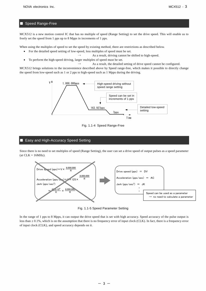
Speed Range-Free
MCX512 is a new motion control IC that has no multiple of speed (Range Setting) to set the drive speed. This will enable us to freely set the speed from 1 pps up to 8 Mpps in increments of 1 pps. When using the multiples of speed to set the speed by existing method, there are restrictions as described below.
• For the detailed speed setting of low-speed, less multiples of speed must be set. → As a result, driving cannot be shifted to high-speed. • To perform the high-speed driving, larger multiples of speed must be set. → As a result, the detailed setting of drive speed cannot be configured.
MCX512 brings solutions to the inconvenience described above by Speed range-free, which makes it possible to directly change the speed from low-speed such as 1 or 2 pps to high-speed such as 1 Mpps during the driving.
Fig. 1.1-4 Speed Range-Free
Easy and High-Accuracy Speed Setting
Since there is no need to set multiples of speed (Range Setting), the user can set a drive speed of output pulses as a speed parameter (at CLK = 16MHz).
Fig. 1.1-5 Speed Parameter Setting
In the range of 1 pps to 8 Mpps, it can output the drive speed that is set with high accuracy. Speed accuracy of the pulse output is less than ± 0.1%, which is on the assumption that there is no frequency error of input clock (CLK). In fact, there is a frequency error of input clock (CLK), and speed accuracy depends on it.
Time
V 1,000,000pps
163,927pps
7pps
High-speed driving without speed range setting
Speed can be set in increments of 1 pps
Detailed low-speed setting
Drive speed (pps)=V×R
8,000,000
Acceleration (pps/sec)=A×125× R8,000,000
Jerk (pps/sec2)
= K1062.5 6×
×R
8,000,000
Drive speed (pps) = DV
Acceleration (pps/sec) = AC
Jerk (pps/sec2) = JK
Speed can be used as a parameter
→ no need to calculate a parameter
・・
NOVA electronics Inc. MCX512 - 4
- 4 -
Various Acceleration / Deceleration Drive Mode
Types of acceleration / deceleration driving
Acceleration / deceleration driving can perform the following driving. Constant speed driving Linear acceleration / deceleration driving (symmetry/ non-symmetry) S-curve acceleration / deceleration driving (symmetry/ non-symmetry)
Automatic deceleration start
In position driving of linear acceleration/deceleration (symmetry/non-symmetry) and S-curve acceleration/deceleration (symmetry), the IC calculates the deceleration start point in decelerating, and automatically starts deceleration. (This is not applied to non-symmetry S-curve acceleration/deceleration driving.)
S-curve acceleration/deceleration curve
S-curve acceleration/deceleration uses the method which increases/decreases acceleration or deceleration in a primary line, and the speed curve forms a secondary parabola acceleration/deceleration. In addition, it prevents triangle waveforms by a special method during S-curve acceleration/deceleration.
Fig. 1.1-6 Acceleration / Deceleration Drive Mode
Position Control
MCX512 has two 32-bit position counters: one is a logical position counter that counts the number of output pulses and the other is a real position counter that counts the feedback number of pulses from an external encoder. The current position can be read by data reading commands anytime. By using with synchronous action, the operation can be performed by the activation factor based on position data, such as drive speed change or start/stop of another axis driving at a specified position.
Software Limit
MCX512 has a software limit function that controls driving to stop when the position counter is over a specified range. There are 2 stop types for when the software limit function is enabled: decelerating stop and instant stop.
Constant Speed Driving
Time
V
Rapid Deceleration
Time
V
Time
V
Time
V
Slow Acceleration
P=400000P=200000P=100000
P=50000
Time
V
Rapid Acceleration
SlowDeceleration
Manual Deceleration
Trapezoidal Acceleration/Deceleration Driving(Symmetry)
Trapezoidal Acceleration/Deceleration Driving(Non-Symmetry)
Parabola S-curve Acceleration/Deceleration Driving(Symmetry)
Automatic Deceleration
Parabola S-curve Acceleration/Deceleration Driving(Non-Symmetry)

NOVA electronics Inc. MCX512 - 5
- 5 -
Various Synchronous Actions
Synchronous action is the function that executes a specified action together if a specified activation factor occurs. These synchronous actions can be performed fast and precisely, independent of the CPU. Synchronous action can be set up to 4 sets to each axis. 1 set of synchronous actions is configured with one specified activation factor and one specified action. 15 types of activation factors are provided, such as the passage of a specified position, start/termination of driving, the rising/falling edge of an external signal and expiring of an internal timer. In addition, 28 types of actions are provided, such as start/termination of driving, save the current position counter value to multi-purpose register and writing of a drive speed. When an activation factor of 1 set of any axis occurs, the other 3 sets of the same axis and 1set of another axis, which are total 5sets of actions, can be activated simultaneously. Multiple synchronous action sets can be used in combination, which allows users to develop a wide array of applications.
• Outputs an external signal when passing through a
specified position during the driving. • Saves the current position to a specified register when
an external signal is input during the driving. • Outputs N split pulses from a specified position to the
external during the driving.
Fig. 1.1-7 Synchronous Action
Four Multi-Purpose Registers
MCX512 has four 32-bit length multi-purpose registers in each axis. Multi-purpose register can be used to compare with the current position, speed and timer, and then can read out the status which represents comparison result and can output as a signal. In addition, it can activate a synchronous action according to comparison result or can generate an interrupt. By using with synchronous action, it can save values of current position or speed of during the driving to multi-purpose registers and load values that are saved in multi-purpose registers to the output pulse number or drive speed.
Timer Function
MCX512 is equipped with a timer in each axis, which can set with the range of 1 ~ 2,147,483,647μsec in increments of 1μsec (at CLK = 16MHz). By using with synchronous action, the following operations can be performed precisely.
• Starts driving after specified periods when the driving is finished.
• Starts driving after specified periods after an external signal is input.
• Stops continuous pulse driving after specified periods.
• Times from position A to position B.
Fig. 1.1-8 Timer Function
Axis is passing through the position 15,000
PIO0
Output the pulse signal to the external
Action
Activation Factor
Timer
Termination of driving Start of driving
After 17.35 msecs
Time
V
Time
V
NOVA electronics Inc. MCX512 - 6
- 6 -
Output of Split Pulse
This is a function in each axis that outputs split pulses during the driving, which synchronizes axis driving and performs various operations at specified intervals. The split length, pulse width of a split pulse and split pulse number can be set. By using with synchronous action, the output of split pulses can be started/terminated at a specified position and the split length or pulse width of a split pulse can be changed by an external signal. Split pulses can be output corresponding to an arbitrary axis during interpolation driving.
Fig. 1.1-9 Split Pulse Output
Automatic Home Search Function
This IC is equipped with the function that automatically executes a home search sequence without CPU intervention. The sequence comprises high-speed home search → low-speed home search → encoder Z-phase search → offset drive. Deviation counter clear pulses can be output for a servo motor driver. In addition, the timer between steps which sets stop time among each step is available, and the operation for a home search of a rotation axis is provided.
Servo Motor Feedback Signals
MCX512 has input pins for servo feedback signals such as encoder 2-phase, in-positioning and alarm signals. An output signal for clearing a deviation counter is also available.
Interrupt Signals
MCX512 has 2 interrupt signals (INT0N, INT1N). INT0N signal is used to generate an interrupt by various factors. For example, (1). at the start / finish of a constant speed drive during the acceleration/deceleration driving, (2). at the end of driving, and (3). when the comparison result of a multi-purpose register with a position counter changes. INT1N signal is used to request to transfer next segment data to CPU while continuous interpolation driving is performed.
Driving by External Signals
Driving can be controlled by external signals, which are the relative position driving, continuous pulse driving and manual pulsar driving. This function is used for JOG feed or teaching mode, reducing the CPU load and making operations smooth.
Drive Pulse
Split Pulse Pulse Width
Split LengthSplit Pulse Number
1 2 3

NOVA electronics Inc. MCX512 - 7
- 7 -
Built-in Input Signal Filter
The IC is equipped with an integral type filter in the input step of each input signal. It is possible to set for each input signal whether the filter function is enabled or the signal is passed through. A filter time constant can be selected from 16 types (500nsec ~ 16msec).
Fig. 1.1-10 Built-in Input Signal Filter
Real Time Monitoring
During the driving, the current status such as logical position, real position, drive speed, acceleration/deceleration, status of accelerating/constant speed driving/decelerating/acceleration increasing/acceleration constant/acceleration decreasing and a timer can be read in real time.
CPU Interface
This IC has I2C serial interface bus in addition to the existing 8-bit/16-bit data bus as the interface to connect a host CPU. I2C serial interface bus needs only 2 lines: serial data line (SDA) and serial clock line (SCL), so the user can use such a PICTM microcomputer that has few terminals as a host CPU. I2C bus can be connected with several devices such as MCX512 or EEPROM that have I2C bus interface on the same bus.
Fig. 1.1-11 I2C Serial Interface Bus
Built-in Filter
+LIMIT
+24V
+3.3V MCX512
nLMTP
(Digital Processing)
MotorDrivingCircuit
Drive pulse
SDA
SCL
I C2
MotorDrivingCircuit
Drive pulse
+3.3V
#1
#2
Host CPU MCX512
MCX512

NOVA electronics Inc. MCX512 - 8
- 8 -
1.2 Functional Block Diagram
MCX512 functional block diagram is shown in the Fig. 1.2-1 as below. It comprises control sections of 2 axes, X and Y that have the same function, and interpolation counting sections. In interpolation driving, interpolation is calculated at the timing of basic pulse oscillation of a specified main axis (AX1), which can be performed both in constant and acceleration/deceleration driving. Fig. 1.2-2 is the functional block diagram of each axis control section.
Fig. 1.2-1 MCX512 The Whole Functional Block Diagram
CLK
RESETN
AX1P+AX1P-AX2P+AX2P-
AX1P+AX1P-AX2P+AX2P-
XP+XP-
YP+YP-
XP+XP-
YP+YP-
INT
INT
INT
8 Bit/16Bit
I C2
SCL
RDN
WRN
A3~A0
D15~D0
CSN
SDA
AX1P+AX1P-AX2P+AX2P-
INT1N
INT0N
Parallel BusControlSection
Serial BusControlSection
Command/Data
InterpretationProcessSection
8 stagesPre-buffer
InterpolationControlSection
Linear InterpolationCounting Section
CircularInterpolationCounting Section
Bit PatternInterpolationCounting Section
Pulse
Separate
X-axis Control Section
Main axis pulse
Y-axis Control Section
InterruptGenerator
1
InterruptGenerator
0
16MHz Standard
X-axisI/O
Y-axisI/O

NOVA electronics Inc. MCX512 - 9
- 9 -
Fig. 1.2-2 Block Diagram of X and Y-Axis Control Section (of 1 axis)
Acceleration/DecelerationGenerator
Speed Generator
Pulse Generator
Logical Position Counter
ActionControlSection
32bit
32bit
UP
DOWN
UP
DOWN
Command/DataInterpretationProcessSection
InterruptGenerator
WaveChange
P+
P-
PP/PLS/PA
PM/DIR/PB
LMTP
LMTM
INPOSALARM
EMGN
INT
Automatic HomeSearch Section
SynchronousAction Section
Jerk Generator
Multi-purposeRegister MR3~0
Timer
Split PulseGenerator
31bitSTOP[2:0]
PIO[13:0]
CompareRegister
A : B
Selector
A
B
C
General OutputOUT[7:0]
Drive StatusOutput
SynchronousPulse / MRComparison
Parameter/ModeSetting Register
Command/Data
A
B
SPLTP
Integrated
FilterCT
RP
LP
CV
IntegratedFilter
ECA/PPIN
ECB/PMIN
Main axispulse
P-
P+
To InterpolationSection
External Signal
Note1
Note1: EMGN is in common all axes.
Real Position Counter WaveChange

NOVA electronics Inc. MCX512 - 10
- 10 -
1.3 Specification Table
(CLK=16MHz) Item Subitem Description
Control Axis 2 axes CPU Parallel Bus Connection
16-bit/8-bit bus selectable
CPU Serial Bus Connection
I2C serial interface bus
Interpolation Function Interpolation Commands 2-axis linear interpolation, CW/CCW circular interpolation, 2-axis bit pattern interpolation
Interpolation Range Each axis -2,147,483,646 ~ 2,147,483,646 drive pulse Interpolation Speed 1 pps ~ 8,000,000 pps *11 Interpolation Accuracy ±0.5LSB or less (linear interpolation)
±1LSB or less (circular interpolation)
Other Interpolation Related Functions
・Can select any axis ・Short axis pulse equalization ・Constant vector speed (2-axis simple mode, 2-axis high-accuracy mode selectable) ・Continuous interpolation ・Data buffering by 8 stages preregister ・Single step interpolation
Drive Pulses Output Drive Speed Range 1 pps ~ 8,000,000 pps (When CLK=20MHz: up to 10,000,000 pps)
Initial Speed Range 1 pps ~ 8,000,000 pps Pulse Output Accuracy ±0.1% or less (according to the setting speed) Acceleration Range 1 pps/sec ~ 536,870,911pps/sec Acceleration Increasing / Decreasing Rate Range
1 pps/sec2 ~ 1,073,741,823 pps/sec2 *1
Acceleration / Deceleration Curve
Constant speed, Symmetrical/non-symmetrical linear acceleration/deceleration, Symmetrical/non-symmetrical parabola S-curve acceleration/ deceleration
Drive Pulse Range ・Relative position driving: -2,147,483,646~2,147,483,646 drive pulse ・Absolute position driving: -2,147,483,646~2,147,483,646 drive pulse
*2
Position Driving Decelerating Stop Mode
Automatic deceleration stop/Manual deceleration stop *3
Override Output pulse number and drive speed are changeable during the driving
*4
Driving Commands Relative/Absolute position driving, +/-direction continuous driving
Triangle Form Prevention Can be used both in linear and S-curve acceleration/deceleration Drive Pulse Output Type Independent 2-pulse, 1-pulse 1-direction,
Quadrature pulse and quad edge evaluation, Quadrature pulse and double edge evaluation are selectable
Drive Pulse Output Logic Positive/Negative logical level selectable Drive Pulse Output Pin Possible to pin inversion
Encoder Input Input Pulse Input Type Quadrature pulses input and quad edge evaluation, Quadrature pulses input and double edge evaluation, Quadrature pulses input and single edge evaluation, Up / down pulse input are selectable
Input Pin Possible to pin inversion
NOVA electronics Inc. MCX512 - 11
- 11 -
Position Counter Logical Position Counter Count Range:-2,147,483,648 ~ +2,147,483,647 drive pulse *5 Real Position Counter Count Range:-2,147,483,648 ~ +2,147,483,647 drive pulse *5 Variable Ring Possible to set the count maximum value of each counter
Software Limit Setting Range -2,147,483,647 ~ +2,147,483,647 pulse Stop Mode Decelerating/Instant stop selectable
Multi-Purpose Register
Bit Length, Number of Registers
32-bit length 4 registers per axis
Uses Compare with position, speed and timer value, load data such as position and speed, and save data such as current position, speed and timer value
Timer Number of timers 1 per axis Setting Range 1 ~ 2,147,483,647μsec
Split Pulse Number of signals 1 per axis Split Length 2 ~ 65,535 drive pulse *6 Split Pulse Width 1 ~ 65,534 drive pulse Split Pulse Number 1 ~ 65,535, or up to infinity
Automatic Home Search
Sequence STEP1 high-speed home search → STEP2 low-speed home search → STEP3 encoder Z-phase search → STEP4 offset drive ・Enable/Disable each step and search signal/direction are
selectable
Deviation Counter Clear Output
Clear pulse width within the range of 10μ~20msec, Logical level selectable
Timer between Steps 1msec ~ 1,000msec selectable Synchronous Action Number of Sets 4 sets per axis *7
Activation Factor ・When multi-purpose register comparison changed ・Comparative object: logical/real position counter value,
current drive speed, current timer value ・Comparison condition: ≧,>,=,< ・When a timer is up ・Start/Termination of driving, Start/Termination of driving at constant speed area in acceleration/deceleration driving
・Start/Termination of split pulse, Output of split pulse ・nPIOm signal ↑/↓, nPIOm+4 signal Low and nPIOm signal ↑, nPIOm+4 signal Hi and nPIOm signal ↑, nPIOm+4 signal Low and nPIOm signal ↓, nPIOm+4 signal Hi and nPIOm signal ↓ (m:0,1,2,3)
・Activation command
Action ・Load value (MRm→setting value):Drive speed, Drive pulse number (Finish point), Split length, Split pulse width, Logical/Real position counter value, Initial speed, Acceleration
・Save value (MRm←current value):Logical/Real position counter value, Current timer value, Current drive speed, Current acceleration/deceleration
・Synchronous pulse output to the external ・Start of relative/absolute position driving, Start of +/-direction continuous driving, Start of relative/absolute position driving by the position data set to MRm
・Decelerating/Instant stop, Speed increase/decrease, Timer-start/stop, Start/Termination of split pulse
Other SYNC Activation Activation of other 3 sets actions can be set. Other Axes SYNC0 Activation Activation of another SYNC0 action can be set. Repeat Synchronous action can be operated once/repeatedly.

NOVA electronics Inc. MCX512 - 12
- 12 -
Interrupt Number of Signals 2: INT0N, INT1N Interrupt Factor ・When multi-purpose register comparison changed
・Comparative object: logical/real position counter value, current drive speed, current timer value
・Comparison condition: ≧,>,=,< ・Start/Termination of driving, Start/Termination of
acceleration/deceleration driving at constant speed ・When automatic home search is finished, When a timer is up ・Termination of split pulse, ・When synchronous action 0 / 1 / 2 / 3 is activated ・When the state of 8 stages of pre-buffer register changes (in continuous interpolation driving).
Enable/Disable Enable/Disable each interrupt factor is selectable External Signal for Driving
・Relative position/Continuous driving by EXPP, EXPM signals ・Manual pulsar (encoder input: quadrature pulses input and single edge evaluation)
*8
External Stop Signal Number of Signals 3 signals (STOP0 ~ 2) per axis Enable/Disable Enable/Disable stop signal function is selectable *9 Logical Level Low/Hi active is selectable Stop Mode When it is active, decelerating stop
(When driving under initial speed, instant stop)
Servo Motor Input/Output Signal
Signals Each axis: ALARM (alarm), INPOS (in-position), DCC (deviation counter clear)
Enable/Disable Enable/Disable a signal is selectable. Logical Level Low/Hi active is selectable.
General Input/Output Signal
Number of Signals 14 signals per axis ・Synchronous input, pins share the input pin for driving by external signals.
・Synchronous action output, multi-purpose register comparison output, pins share drive status output signal pins.
Driving Status Output Signal
Signals ・Driving, Error, Accelerating, Constant speed driving, Decelerating, Acceleration increasing, Acceleration constant, Acceleration decreasing
・Drive status can also be read by status register.
*10
Over Limit Signal Number of Signals 2 signals per axis (for each + and - direction) Enable/Disable Enable/Disable limit function is selectable. *9
Logical Level Low/Hi active is selectable. Stop Mode Decelerating stop or instant stop is selectable when it is active. Input Pin Possible to pin inversion
Emergency Stop Signal
EMGN 1 signal for all axes, stops drive pulse output at Low level. (Logical level cannot be set)
Integral Type Filter Input Signal Filter Equipped with integral filters in the input column of each input signal. Time Constant Time constant can be selected from 16 types. (500n,1μ,2μ,4μ,
8μ,16μ,32μ,64μ,128μ,256μ,512μ,1m,2 m,4 m,8 m,16 m[sec])
Enable/Disable Enable/Disable filter function is selectable. Electrical Characteristics
Operating Temperature -40~+85 Operating Power Voltage +3.3V ±10% Consumption Current 45mA (average), 50mA(max) at CLK=16MHz Input Clock Pulse 16MHz (standard) 20MHz (max) Input Signal Level TTL level (5V tolerant) Output Signal Level 3.3V CMOS Level (only TTL can be connected to 5V type)
Package ・100-pin plastic QFP, pin pitch:0.5mm, RoHS compliant ・Dimension: 14×14×1.4 mm
NOVA electronics Inc. MCX512 - 13
- 13 -
<Further Note>
*1 Parameter that is used in S-curve acceleration / deceleration driving.
*2 Pulse range that can be set for the driving that outputs specified pulses. In continuous driving, pulses are output up to infinity.
*3
Automatic deceleration stop performs decelerating stop automatically by calculating the deceleration start point based on specified drive pulses. Manual deceleration stop performs decelerating stop by setting the deceleration start point from the high order. This IC can perform automatic deceleration stop except for non-symmetrical S-curve acceleration / deceleration.
*4 After the start of driving, output pulse number can be changed for the same direction in only relative position driving. The drive speed cannot be changed during continuous interpolation driving.
*5 Logical position counter counts output pulses and real position counter counts encoder input pulses. *6 While driving, split pulses are output at specified intervals in synchronization with driving pulses. *7 1 set of synchronous actions is configured with one specified activation factor and one specified action. *8 Input pins for external signals share the general purpose input/output pins. *9 When the function is not used, it can be used as general purpose input.
*10 Drive status output signal pins share the general purpose input/output pins. *11 Bit pattern and continuous interpolation are 4Mpps or less.

NOVA electronics Inc. MCX512 - 14
- 14 -
2. The Descriptions of Functions
2.1 Fixed Pulse Driving and Continuous Pulse Driving
There are two kinds of pulse output commands: fixed pulse driving that is performed based on the number of output pulses predetermined and continuous pulse driving that outputs pulses until a stop command is written or stop signal is input. Fixed pulse driving has relative position driving, absolute position driving and counter relative position driving. Continuous pulse driving has +direction continuous pulse driving and -direction continuous pulse driving.
• Fixed pulse driving ・ Relative position driving ・ Absolute position driving ・ Counter relative position driving
• Continuous pulse driving ・ +Direction continuous pulse driving ・ -Direction continuous pulse driving
2.1.1 Relative Position Driving Relative position driving performs the driving by setting the drive pulse number from the current position. To drive from the current position to the +direction, set the positive pulse number in the drive pulse number, and to the -direction, set the negative pulse number in the drive pulse number.
Fig. 2.1-1 Setting Example of Drive Pulse Number (TP) in Relative Position Driving
Relative position driving performs constant speed driving or acceleration/deceleration driving. Relative position driving in the acceleration/deceleration where acceleration and deceleration are equal, as shown in Fig. 2.1-2, automatic deceleration starts when the number of pulses becomes less than the number of pulses that were utilized at acceleration, and driving terminates when the output of specified drive pulses is completed.
Fig. 2.1-2 Auto Deceleration and Stop in Relative Position Driving
Command code for relative position driving is 50h. To perform relative position driving in linear acceleration/deceleration, the following parameters must be set.
Table 2.1-1 Setting Parameters:Relative Position Driving
Parameter Symbol Comment
Acceleration/Deceleration AC/DC No need to set deceleration when acceleration and deceleration are equal.
Initial speed SV Drive speed DV
Drive pulse number/ Finish point
TP Set +pulse number for the +direction. Set -pulse number for the -direction.
Current position
+direction-direction
To the+direction20,000 pulses
To the-direction20,000 pulses
TP:-20,000 TP:+20,000
Speed
timeInitial Speed
Driving Speed
Auto Deceleration
Stop SpecificOutput Pulse

NOVA electronics Inc. MCX512 - 15
- 15 -
2.1.2 Absolute Position Driving Absolute position driving performs the driving by setting the destination point based on a home (logical position counter = 0). The destination point can be set by absolute coordinates regardless of the current position. The IC calculates drive direction and output pulse number according to the difference between the specified destination point and current position, and then performs the driving. In absolute position driving, the destination point should be set by absolute coordinates within the range of driving space. So, the user first needs to perform automatic home search to determine the logical position counter before driving.
Fig. 2.1-3 Example of Specifying Finish Point (TP) in Absolute Position Driving
Absolute position driving performs constant speed driving or acceleration/deceleration driving as well as relative position driving. Command code for absolute position driving is 54h. To perform absolute position driving in linear acceleration/deceleration, the following parameters must be set.
Table 2.1-2 Setting Parameters:Absolute Position Driving
Parameter Symbol Comment
Acceleration/Deceleration AC/DC No need to set deceleration when acceleration and deceleration are equal
Initial speed SV Drive speed DV
Drive pulse number/ Finish point
TP Set the destination point by absolute coordinates.
2.1.3 Counter Relative Position Driving Counter relative position driving performs the driving by setting the direction and drive pulse number to the destination point based on the current position. Unlike relative position driving, driving is performed in a direction opposite to the sign of the pulse number that is set to drive pulse number (TP). This is useful for when the user wants to determine a drive direction using a driving command, by setting the predetermined positive value to the drive pulse number in advance. If the negative value is set to the drive pulse number, counter relative position driving performs the driving in the +direction.
Fig. 2.1-4 Driving Direction is Determined by Relative/Counter Relative Position Driving Command
The operation of counter relative position driving is the same as relative position driving except the operation which drives in a direction opposite to the sign of the pulse number that is set in drive pulse number (TP). Command code for counter relative position driving is 51h.
0 +10,000 +20,000 [Absolute coordinates]-20,000 -10,000
TP:+20,000TP:-20,000
(Home)
Current position
Counter relative positiondriving command (51h)
Relative positiondriving command (50h)
Drive pulse number(TP)=20,000To the-direction20,000 pulses
To the+direction20,000 pulses
+direction-direction
Current position

NOVA electronics Inc. MCX512 - 16
- 16 -
Changing Drive Pulse Number in the middle of Driving (Override)
The drive pulse number (TP) can be changed during relative position driving and counter relative position driving. However, the drive direction must be the same before and after the change of drive pulse number. The drive pulse number cannot be changed to the value of different direction.
Fig. 2.1-5 Override Drive Pulse Number (TP) in Relative Position Driving
In acceleration/deceleration driving, if the rest of output pulses become less than the pulses at acceleration, and the drive pulse number (TP) is changed during deceleration, the driving accelerates again (Fig. 2.1-7). And if the output pulse number of changed drive pulse number (TP) is less than the number of pulses already output, the driving stops immediately (Fig. 2.1-8). In S-curve acceleration/deceleration driving, if the drive pulse number (TP) is changed during deceleration, the S-curve profile cannot be exactly tracked.
Fig. 2.1-6 Change of Drive Pulse Number in Driving Fig. 2.1-7 Change of Drive Pulse Number in Deceleration
Fig. 2.1-8 Changing Drive Pulse Number Less than Output Pulse Number
[Note] The drive pulse number (TP) cannot be changed while Absolute position driving.
Manual Deceleration for Fixed Pulse Acceleration/Deceleration Driving
As shown in Fig. 2.1-2, generally the deceleration of fixed pulse driving (relative position driving, absolute position driving and counter relative position driving) is controlled automatically by MCX512. However, in the following situations, it should be preset the deceleration point by the users.
• The change of speed is too often in the trapezoidal acceleration/deceleration fixed pulse driving.
TP:+20,000 in relative position driving
TP changed
TP:+30,000
TP:+10,000
TP:-10,000 …NG!
TP in the other direction cannot be changed
+direction-direction
Change of Drive Pulse Number
Speed
time
Speed
time
Change of Drive Pulse Number
Speed
time
Change ofDrive Pulse Number

NOVA electronics Inc. MCX512 - 17
- 17 -
• Speed is changed during the driving in the non-symmetry trapezoidal acceleration/deceleration and S-curve acceleration/deceleration fixed pulse driving.
• Acceleration, deceleration, jerk (acceleration increasing rate) and deceleration increasing rate are set individually for S-curve acceleration/deceleration fixed pulse driving (non-symmetry S-curve acceleration/deceleration).
• Circular interpolation, bit pattern interpolation and continuous interpolation are performed in acceleration/deceleration. To perform manual deceleration mode, please set D0 bit of WR3 register to 1, and use manual decelerating point setting command (07h) to set a deceleration point. As to other operations, the setting is the same as those of fixed pulse driving.
Offset Setting for Acceleration/Deceleration Driving
The offset function can be used for compensating the pulses when the decelerating speed does not reach the setting initial speed during acceleration/deceleration fixed pulse driving. MCX512 will calculate the acceleration/deceleration point automatically, and arrange the output pulses of deceleration phase that is equal to those of acceleration phase. When setting the offset for deceleration, MCX512 will start deceleration early for the offset. The greater positive value is set for the offset, the closer the automatic declaration point becomes, for this reason creep pulses of the initial speed will increase at the termination of deceleration. If a negative value is set for the offset, output may stop prematurely before the speed reaches the initial speed (see Fig. 2.1-9).
Fig. 2.1-9 Offset for Deceleration
The default value for the offset is 0 when MCX512 power-on reset. It is not necessary to change the shift pulse value in normal acceleration/deceleration fixed pulse driving. As for fixed pulse driving in non-symmetrical trapezoidal acceleration/deceleration or S-curve acceleration/deceleration, if creep pulses or premature termination occurs at the termination of driving due to the low initial speed, correct by setting the acceleration counter offset appropriately. 2.1.4 Continuous Pulse Driving When continuous pulse driving is performed, MCX512 will drive pulse output in a specific speed until a stop command or external stop signal becomes active. The user can use it for: home searching, teaching and speed control. There are two stop commands, one is “decelerating stop” and the other is “instant stop”. And three input pins nSTOP0 ~ nSTOP2 can be connected for external decelerating stop (instant stop when driving under initial speed) signal. Enable/disable and active level can be set in mode setting.
Fig. 2.1-10 Continuous Pulse Driving
+ Direction continuous pulse driving command (52h) and - Direction continuous pulse driving command (53h) are available. To perform acceleration/deceleration continuous pulse driving, parameters except drive pulse number (TP) must be set as well as fixed pulse driving.
Offset Pulse
Speed
timeInitial Speed
Stop Command orExternal Stop Signal
Speed
timeInitial Speed
Drive Speed
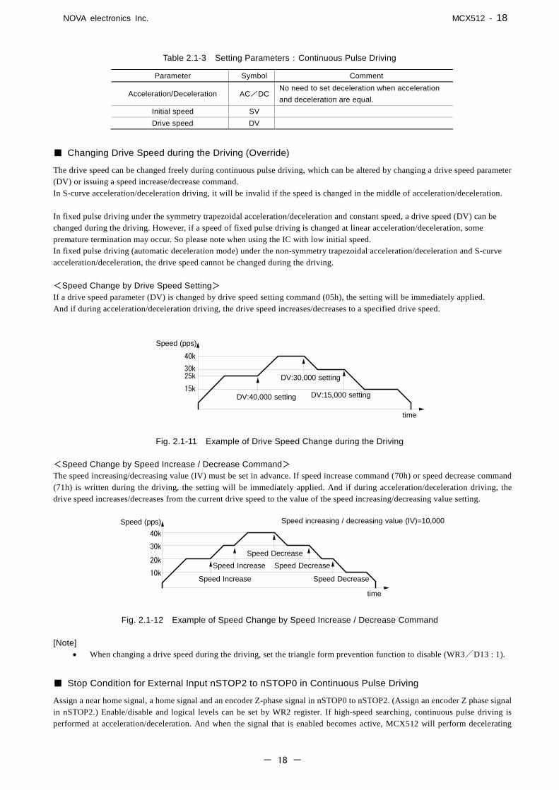
NOVA electronics Inc. MCX512 - 18
- 18 -
Table 2.1-3 Setting Parameters:Continuous Pulse Driving
Parameter Symbol Comment
Acceleration/Deceleration AC/DC No need to set deceleration when acceleration and deceleration are equal.
Initial speed SV Drive speed DV
Changing Drive Speed during the Driving (Override)
The drive speed can be changed freely during continuous pulse driving, which can be altered by changing a drive speed parameter (DV) or issuing a speed increase/decrease command. In S-curve acceleration/deceleration driving, it will be invalid if the speed is changed in the middle of acceleration/deceleration. In fixed pulse driving under the symmetry trapezoidal acceleration/deceleration and constant speed, a drive speed (DV) can be changed during the driving. However, if a speed of fixed pulse driving is changed at linear acceleration/deceleration, some premature termination may occur. So please note when using the IC with low initial speed. In fixed pulse driving (automatic deceleration mode) under the non-symmetry trapezoidal acceleration/deceleration and S-curve acceleration/deceleration, the drive speed cannot be changed during the driving. <Speed Change by Drive Speed Setting> If a drive speed parameter (DV) is changed by drive speed setting command (05h), the setting will be immediately applied. And if during acceleration/deceleration driving, the drive speed increases/decreases to a specified drive speed.
Fig. 2.1-11 Example of Drive Speed Change during the Driving
<Speed Change by Speed Increase / Decrease Command> The speed increasing/decreasing value (IV) must be set in advance. If speed increase command (70h) or speed decrease command (71h) is written during the driving, the setting will be immediately applied. And if during acceleration/deceleration driving, the drive speed increases/decreases from the current drive speed to the value of the speed increasing/decreasing value setting.
Fig. 2.1-12 Example of Speed Change by Speed Increase / Decrease Command
[Note] • When changing a drive speed during the driving, set the triangle form prevention function to disable (WR3/D13 : 1).
Stop Condition for External Input nSTOP2 to nSTOP0 in Continuous Pulse Driving
Assign a near home signal, a home signal and an encoder Z-phase signal in nSTOP0 to nSTOP2. (Assign an encoder Z phase signal in nSTOP2.) Enable/disable and logical levels can be set by WR2 register. If high-speed searching, continuous pulse driving is performed at acceleration/deceleration. And when the signal that is enabled becomes active, MCX512 will perform decelerating
15k
25k30k
40k
DV:40,000 setting
DV:30,000 setting
DV:15,000 setting
Speed (pps)
time
10k
20k
30k
40k
Speed Increase
Speed increasing / decreasing value (IV)=10,000
Speed Decrease
Speed Increase Speed DecreaseSpeed Decrease
Speed (pps)
time

NOVA electronics Inc. MCX512 - 19
- 19 -
stop. If low-speed searching, continuous pulse driving is performed at constant speed. And when the signal that is enabled becomes active, MCX512 will perform instant stop. This IC has automatic home search function. See chapter 2.5 for details of automatic home search function.
2.2 Acceleration and Deceleration
There are the following speed curves that can trace from drive pulse output: Constant speed driving which does not perform acceleration/deceleration, Trapezoidal acceleration/deceleration driving which performs linear acceleration/deceleration to a setting speed, and S-curve acceleration/deceleration driving which performs acceleration/deceleration to a specified drive speed with a smooth curve. And the following acceleration/deceleration driving is each available: Symmetry acceleration/deceleration where acceleration and deceleration are equal and Non-symmetry acceleration/deceleration where acceleration and deceleration are set individually.
Constant speed driving
Acceleration/Deceleration driving • Trapezoidal acceleration/deceleration driving
・ Linear acceleration/deceleration (Symmetry) ・ Non-symmetry linear acceleration/deceleration
• S-curve acceleration/deceleration driving ・ S-curve acceleration/deceleration (Symmetry) ・ Non-symmetry S-curve acceleration/deceleration
2.2.1 Constant Speed Driving Constant speed driving outputs drive pulses at a constant speed without acceleration/deceleration. To perform constant speed driving, the drive speed must be set lower than the initial speed (that is the initial speed is higher than the drive speed.). Constant speed driving performs the driving at the drive speed lower than the initial speed without acceleration/deceleration. Stop mode is instant stop. If the user wants to stop immediately when the home sensor or encoder Z-phase signal is active, perform the low-speed constant speed driving from the beginning not acceleration/deceleration driving.
Fig. 2.2-1 Constant Speed Driving
To perform constant speed driving, the following parameters must be set.
Table 2.2-1 Setting Parameters:Constant Speed Driving
Parameter Symbol Comment Initial speed SV Set higher than the drive speed (DV). Drive speed DV
Drive pulse number/ Finish point
TP Not required for continuous pulse driving.
Speed
time
Initial Speed
Drive Speed

NOVA electronics Inc. MCX512 - 20
- 20 -
Example for Parameter Setting of Constant Speed
The constant speed is set 980 PPS as shown in Fig. 2.2-2 below. In this case, the relative position driving that the drive pulse number is 2450 is performed.
Initial speed SV = 980 Set the value which initial speed ≧ Drive speed
Drive speed DV = 980 Drive pulse number
TP = 2450
Please refer each parameter in chapter 7.2. 2.2.2 Trapezoidal Driving [Symmetrical] In linear acceleration/deceleration driving, the driving accelerates from the initial speed at the start of driving to the drive speed in a primary linear form with a specified acceleration slope. Linear acceleration/deceleration driving can decelerate automatically and no need to set a decelerating point. In fixed pulse driving under the symmetry trapezoidal acceleration/deceleration where acceleration and deceleration are equal, it counts the number of pulses that were utilized at acceleration and automatic deceleration starts when the rest of output pulses become less than the pulses at acceleration. Deceleration continues in the primary line with the same slope as that of acceleration until the speed reaches the initial speed, and then driving will stop at the completion of the output all pulses. If the decelerating stop command is performed during acceleration, the driving will start to decelerate in the middle of acceleration, as show in Fig. 2.2-3.
Fig. 2.2-3 Trapezoidal Driving (Symmetry)
To perform symmetry linear acceleration/deceleration driving using automatic deceleration, D2 ~ 0 bits of WR3 register and the following parameters must be set.
Table 2.2-2 Mode Setting:Linear Acceleration/Deceleration (Symmetry)
Mode Setting Bit Symbol Setting Comment WR3/D0 MANLD 0 Automatic deceleration WR3/D1 DSNDE 0 When in deceleration, acceleration setting value is used (symmetry). WR3/D2 SACC 0 Linear acceleration/deceleration
Table 2.2-3 Setting Parameters:Linear Acceleration/Deceleration (Symmetry)
Parameter Symbol Comment Acceleration AC When in deceleration, this value is used to decelerate. Initial speed SV Drive speed DV
Drive pulse number / Finish point TP Not required for continuous pulse driving.
Decelerating stop isperformed during acceleration
Acceleration (slope)Deceleration = Acceleration
Speed
time
Initial Speed
Drive Speed
980
2.50
Speed(pps)
time (sec)
Fig. 2.2-2 Example of Constant Speed Driving

NOVA electronics Inc. MCX512 - 21
- 21 -
Example for Parameter Setting of Trapezoidal Driving
As shown in the figure right hand side, acceleration is formed from the initial speed 500 PPS to 15,000 PPS in 0.3 sec.
Fig. 2.2-4 Example of Trapezoidal Driving (Symmetry) Please refer each parameter in chapter 7.2.
Triangle Form Prevention of Trapezoidal Driving (Fixed Pulse Driving)
The triangle form prevention function prevents a triangle form in linear acceleration/deceleration fixed pulse driving even if the number of output pulses does not reach the number of pulses required for accelerating to a drive speed. The triangle form indicates the speed curve that shifts to deceleration during the acceleration phase in linear acceleration/deceleration driving. When the number of pulses that were utilized at acceleration and deceleration exceeds 1/2 of the total number of output pulses during acceleration, this IC stops acceleration and keeps that driving speed and then decelerates automatically. Therefore, even if the number of output pulses is less in fixed pulse driving, 1/2 of the number of output pulses becomes constant speed area and can make the triangle form into the trapezoidal form.
Fig. 2.2-5 Triangle Prevention of Linear Acceleration/Decelerating Driving
The triangle form prevention function in linear acceleration/deceleration fixed pulse driving is enabled from a reset. And it can be disabled by setting D13 bit of WR3 register to 1. If the decelerating stop command is performed during acceleration, the triangle form prevention does not work. As shown in Fig. 2.2-3, deceleration starts from when the decelerating stop is performed. [Note]
• When changing a drive speed during the driving, set the triangle form prevention function to disable (WR3/D13 : 1).
15,000
500
0.3
Speed(pps)
time (sec)
AcceleratingStop
Pa Pa+Pd Pd
P = 2×(Pa+Pd)P :Output pulse number in fixed drivingPa:Number of pulses utilized at accelerationPd:Number of pulses utilized at deceleration
Speed
time
Acceleration AC = 48333
(15000-500)/0.3 = 48333pps/sec
Initial speed SV = 500
Drive speed DV = 15000
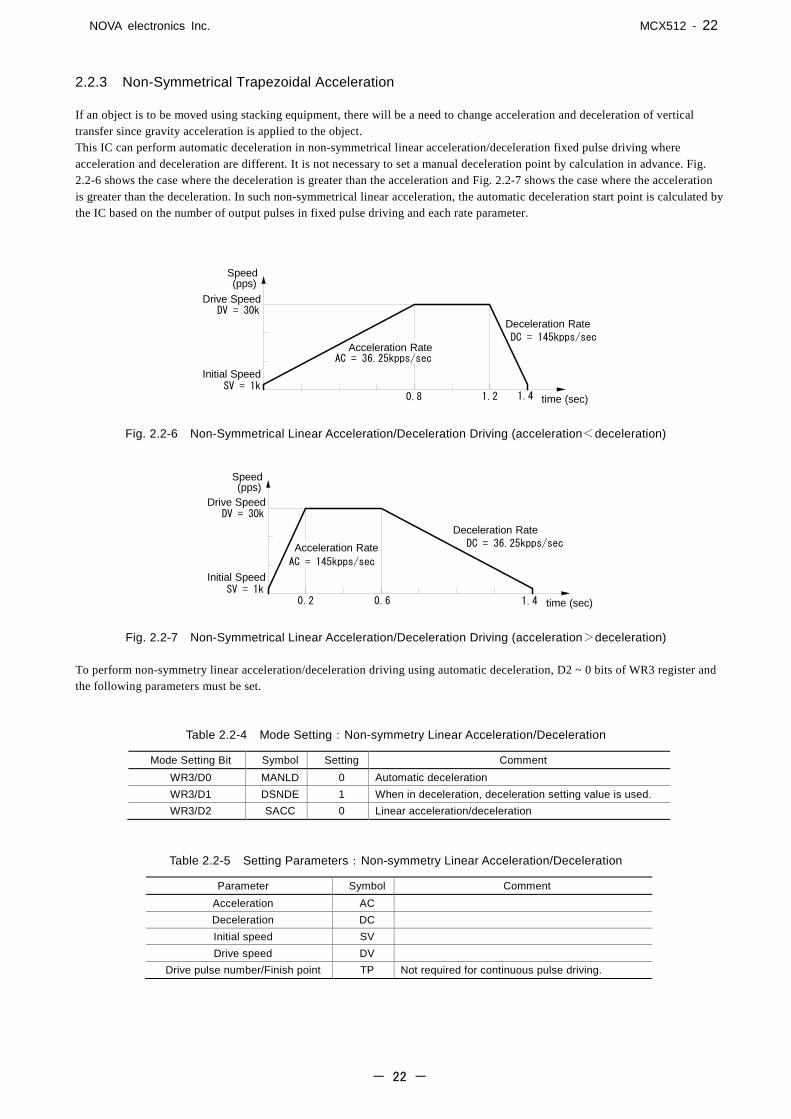
NOVA electronics Inc. MCX512 - 22
- 22 -
2.2.3 Non-Symmetrical Trapezoidal Acceleration If an object is to be moved using stacking equipment, there will be a need to change acceleration and deceleration of vertical transfer since gravity acceleration is applied to the object. This IC can perform automatic deceleration in non-symmetrical linear acceleration/deceleration fixed pulse driving where acceleration and deceleration are different. It is not necessary to set a manual deceleration point by calculation in advance. Fig. 2.2-6 shows the case where the deceleration is greater than the acceleration and Fig. 2.2-7 shows the case where the acceleration is greater than the deceleration. In such non-symmetrical linear acceleration, the automatic deceleration start point is calculated by the IC based on the number of output pulses in fixed pulse driving and each rate parameter.
Fig. 2.2-6 Non-Symmetrical Linear Acceleration/Deceleration Driving (acceleration<deceleration)
Fig. 2.2-7 Non-Symmetrical Linear Acceleration/Deceleration Driving (acceleration>deceleration)
To perform non-symmetry linear acceleration/deceleration driving using automatic deceleration, D2 ~ 0 bits of WR3 register and the following parameters must be set.
Table 2.2-4 Mode Setting:Non-symmetry Linear Acceleration/Deceleration
Mode Setting Bit Symbol Setting Comment WR3/D0 MANLD 0 Automatic deceleration WR3/D1 DSNDE 1 When in deceleration, deceleration setting value is used. WR3/D2 SACC 0 Linear acceleration/deceleration
Table 2.2-5 Setting Parameters:Non-symmetry Linear Acceleration/Deceleration
Parameter Symbol Comment Acceleration AC Deceleration DC Initial speed SV Drive speed DV
Drive pulse number/Finish point TP Not required for continuous pulse driving.
DC = 145kpps/sec
Deceleration RateDV = 30k
SV = 1k0.8 1.2 1.4
Acceleration RateAC = 36.25kpps/sec
Speed(pps)
time (sec)
Initial Speed
Drive Speed
DC = 36.25kpps/sec
1.40.2 0.6
AC = 145kpps/sec
DV = 30k
SV = 1k
Speed(pps)
time (sec)
Initial Speed
Drive Speed
Deceleration Rate
Acceleration Rate

NOVA electronics Inc. MCX512 - 23
- 23 -
[Note] • In non-symmetry linear automatic acceleration/deceleration driving, when acceleration>deceleration (Fig. 2.2-7), the
following condition is applied to the ratio of acceleration and deceleration. In this case, set drive speed 4Mpps or less.
6108
DVACDC
××>
For instance, if the driving speed DV = 100kpps, deceleration DC must be greater than 1/80 of acceleration AC. The value must not be less than 1/80 of acceleration.
• In non-symmetry linear automatic acceleration/deceleration driving, if acceleration > deceleration (Fig. 2.2-7), the greater the ratio of acceleration AC to deceleration DC becomes, the greater the number of creep pulses becomes (about maximum of 10 pulses when AC/DC=10 times). When creep pulses cause a problem, solve the problem by increasing the initial speed or setting a minus value to the acceleration counter offset.
Example of Parameter Setting
As shown in Fig. 2.2-6, parameter setting of relative position driving in non-symmetrical linear automatic acceleration/ deceleration (acceleration<deceleration) is shown below.
Mode setting WR3←0002h Mode setting of WR3 register Acceleration AC = 36250 (30000-1000)/0.8 = 36250pps/sec Deceleration DC = 145000 (30000-1000)/0.2 = 145000pps/sec Initial speed SV = 1000 Drive speed DV = 30000 Drive pulse number TP = 27500 Relative position driving
DC:Deceleration (pps/sec) AC:Acceleration (pps/sec) When CLK = 16MHz DV:Drive speed (pps)

NOVA electronics Inc. MCX512 - 24
- 24 -
2.2.4 S-curve Acceleration/Deceleration Driving [Symmetrical] S-curve acceleration/deceleration driving performs acceleration and deceleration to a specified drive speed with a smooth curve that forms a secondary parabolic curve. This IC creates an S-curve by increasing/reducing acceleration/deceleration in a primary line at acceleration and deceleration of drive speed. Fig. 2.2-8 shows the operation of S-curve acceleration/deceleration driving where acceleration and deceleration are symmetrical.
Section a. When driving starts, the acceleration increases on a straight line at a specified jerk. In this case, the speed data forms a quadratic curve. Section b. If the difference between a specified drive speed and the current speed becomes less than the speed that was utilized at acceleration increasing, the acceleration starts to decrease on a straight line at a specified jerk. The decrease ratio is the same as the increase ratio. In this case, the rate curve forms a parabola of reverse direction. Section c. When the speed reaches a specified drive speed or the acceleration reaches 0, the driving keeps that speed.
In fixed pulse driving of S-curve acceleration/deceleration where acceleration and deceleration are symmetrical, when the rest of output pulses becomes less than the number of pulses that were utilized at acceleration, deceleration starts (automatic deceleration).
Section d,e. Also in deceleration, the speed forms an S-curve by increasing/decreasing deceleration in a primary linear form. The same operation is performed in acceleration/deceleration where the drive speed is changed during continuous pulse driving. However, in S-curve acceleration/deceleration driving, change of a drive speed during acceleration/deceleration is invalid.
Fig. 2.2-8 S-curve Acceleration/Deceleration Driving (Symmetry)
To perform symmetry S-curve acceleration/deceleration driving using automatic deceleration, D2 ~ 0 bits of WR3 register and the following parameters must be set.
Table2.2-6 Mode Setting:S-curve Acceleration / Deceleration (Symmetry)
Mode Setting Bit Symbol Setting Comment WR3/D0 MANLD 0 Automatic deceleration WR3/D1 DSNDE 0 When in deceleration, acceleration and jerk setting values are used. WR3/D2 SACC 1 S-curve acceleration/deceleration
Table 2.2-7 Setting Parameters:S-curve Acceleration/Deceleration (Symmetry)
Parameter Symbol Comment Jerk JK
Acceleration AC Set the maximum value:536,870,911 (1FFF FFFFh). Initial speed SV Drive speed DV
Drive pulse number/Finish point TP Not required for continuous pulse driving.
Acceleration/ Deceleration
a b c d e
Acceleration Deceleration
Acceleration increasing rate (slope)
Speed
timeInitial Speed
Drive Speed
time

NOVA electronics Inc. MCX512 - 25
- 25 -
Triangle Form Prevention of S-curve Acceleration/Deceleration Driving
S-curve acceleration/deceleration driving also has the triangle form prevention function for keeping a speed curve smooth. In fixed pulse driving of S-curve acceleration/deceleration where acceleration and deceleration are symmetrical, when the number of output pulses does not reach the number of pulses required for accelerating to a drive speed or when decelerating stop is performed during S-curve acceleration, the triangle form prevention function works in both cases and keeps a speed curve smooth. <The Prevention of Triangle Driving Profile in Fixed Pulse Driving>
In fixed pulse driving of S-curve acceleration/deceleration where acceleration and deceleration are symmetrical, when the number of output pulses does not reach the number of pulses required for accelerating to a drive speed, the following method is applied to keep a speed curve smooth.
Fig. 2.2-9 The Rule of 1/12 of S-curve Acceleration/Deceleration
If the initial speed is "0" and the acceleration is increased up to the time "t" at a constant jerk "a", in the section of acceleration increasing, the speed "v(t)" in the time "t" can be expressed as follows.
2atv(t) = a: coefficient related to speed
Therefore, the total number of pulses “p(t)” utilized during the time from “0” to “t” is the integral of the speed “v(t)” from the time “0” to “t”.
3at3
1p(t) ×=
This value indicates 1/3 of at2×t (the number of pulses of one square on the figure) regardless of the value of the jerk. In fixed pulse driving, the acceleration is increased from the time “0” to “t” at a specified jerk, and is decreased from the time “t” at the same jerk. When the acceleration reaches 0, and if the deceleration is also increased/decreased at the same jerk, the number of pulses that were utilized in fixed pulse driving is expressed, as shown in Fig. 2.2-9, as follows.
43
1
3
211
3
2
3
1=+++++ squares on the figure
Therefore, the number of pulses (1/3 of a square) that were utilized during the time from “0” to “t” in acceleration increasing section is 1/12 of pulses that were utilized in all fixed pulse driving. For this reason, in S-curve acceleration/deceleration fixed pulse driving, when the number of output pulses during acceleration is more than 1/12 of total output pulses, MCX512 will stop increasing acceleration and start to decrease the acceleration value with the speed curve as shown in Fig. 2.2-9. [Rule of 1/12] This method makes an ideal curve when the initial speed is 0, however the initial speed cannot be 0, so the pulses from 0 on the figure to the initial speed will be excess and will be output at the peak of the speed.

NOVA electronics Inc. MCX512 - 26
- 26 -
<The Prevention of Triangle Driving Profile in Decelerating Stop>
In linear acceleration/deceleration driving, if the decelerating stop is commanded during acceleration, the speed curve forms a triangle form. In S-curve acceleration/deceleration driving, if the decelerating stop is commanded during acceleration as shown in Fig. 2.2-10, deceleration starts after the acceleration reaches 0.
Fig. 2.2-10 Triangle Prevention of S-curve Acceleration/Deceleration by Decelerating Stop
Constraints for S-curve Acceleration/Deceleration Driving
a. The drive speed cannot be changed during S-curve acceleration/deceleration fixed pulse driving. b. In S-curve acceleration/deceleration fixed pulse driving, if the drive pulse number is changed during deceleration, the S-
curve profile cannot be exactly tracked. c. In S-curve acceleration/deceleration fixed pulse driving, if an extremely low value is set as the initial speed, premature
termination (output of specified driving pulses is completed and terminated before the speed reaches the initial speed) or creep (output of specified driving pulses is not completed even if the speed reaches the initial speed and the rest of driving pulses is output at the initial speed) may occur.
d. The drive speed can be changed during S-curve acceleration/deceleration continuous pulse driving. However, the command to change the drive speed during acceleration/deceleration will be invalid. To change the speed in S-curve acceleration/deceleration continuous pulse driving, make sure to change it during constant speed driving (RR3 register Page1 CNST=1). Speed increase/speed decrease (70h, 71h) commands and speed change by synchronous action will also be invalid.
①Request for Deceleration Stop
②Decrease the Acceleration value
③Deceleration starts when Acceleration becomes 0
Acceleration/ Deceleration
Speed
time
time

NOVA electronics Inc. MCX512 - 27
- 27 -
Example of Parameter Setting (Symmetry S-Curve Acceleration / Deceleration)
The figure shown below is the example of S-curve acceleration that reaches from the initial speed 100pps to the drive speed 40kpps in 0.4 seconds.
Fig. 2.2-11 Example of Symmetry S-Curve Acceleration / Deceleration Driving
At acceleration, acceleration is increased on a straight line based on a specified jerk (JK). The integral value (area indicated by diagonal lines) is the increased value of the speed from the initial speed “SV”. Find the jerk (JK) to produce the result where the speed reaches a half ((DV-SV)/2) of the drive speed (DV) from the initial speed (SV) within a half (t/2) of the acceleration time (t=0.4sec). Use the following expression to find a value of “JK” since the area indicated by diagonal lines which uses “JK” in the left-hand member, is equal to the right-hand member.
2
SVDV
2
tJK
2
12
−=
××
2t
SV)4(DVJK
−=
997,5000.4
100)4(40000JK
2=
−= pps/sec2
Therefore, the parameters for S-curve acceleration/deceleration driving with the acceleration as shown in Fig. 2.2-11 are as follows.
Mode Setting WR3 ← 0004h Mode setting of WR3 register Jerk JK = 997500 Acceleration AC = 536870911 Set the maximum value:(1FFF FFFFh) Initial speed SV = 100 Drive speed DV = 40000 Drive pulse number TP = 27500 Set when fixed pulse driving is performed.
SV
DV
t2
t = 0.4sec
JK(slope)
2
DV-SV
2
DV-SV
2
DV-SV
time
time
Speed
Acceleration
Jerk JK [pps/sec2]
Drive speed DV [pps] Initial speed SV [pps] Acceleration time t [sec]

NOVA electronics Inc. MCX512 - 28
- 28 -
Partial S-curve Acceleration/Deceleration
In acceleration/deceleration driving with a linear section of acceleration and deceleration, it is possible to form a smooth S-curve only in the start/end part of acceleration or deceleration. To set the speed parameter for acceleration and deceleration, specify not the maximum value but the value of acceleration and deceleration in a linear section of acceleration/deceleration.
As shown in Fig. 2.2-12, section b,f indicate a linear section of acceleration/deceleration and section a,c,e,g indicate S-curve section of acceleration/deceleration. At section a, the acceleration increases on a straight line from 0 to the acceleration setting value and the speed curve forms a secondary parabolic curve. When the acceleration reaches the acceleration setting value, the acceleration keeps that value and the speed curve forms a straight line in the acceleration of section b. If the difference between a specified drive speed and the current speed becomes less than the speed that was utilized at acceleration increasing, the acceleration starts to decrease at a specified jerk and the speed curve forms a parabola of reverse direction at section c. Also in deceleration, it forms a partial S-curve of deceleration.
Fig. 2.2-12 Partial S-curve Acceleration/Deceleration Driving
Specified Value
a b c e f gd
time
time
Speed
Acceleration/ Deceleration
Initial Speed
Drive Speed
Acceleration Deceleration
Acceleration increasing rate (slope)

NOVA electronics Inc. MCX512 - 29
- 29 -
Example of Parameter Setting (Partial S-curve Acceleration/Deceleration)
The figure shown below is the example of partial S-curve acceleration that reaches to 10kpps in 0.2 seconds by parabolic acceleration and then reaches from 10kpps to 30kpps in 0.2 seconds by acceleration on a straight line, finally reaches from 30kpps to 40kpps in 0.2 seconds by parabolic acceleration. To simplify a calculation, suppose the initial speed is 0. The acceleration increases to the first 10kpps in 0.2 seconds by parabolic acceleration on a straight line, and this integral value (area indicated by diagonal lines) corresponds to the rising speed 10kpps of the first parabolic acceleration. Therefore, the acceleration at 0.2 seconds is 10k×2/0.2=100kpps/sec and the jerk is 100k/0.2=500kpps/sec2.
Fig. 2.2-13 Example of Partial S-curve Acceleration/Deceleration Driving
However the initial speed cannot be 0, the initial speed SV must be set the value larger than 0. In partial S-curve acceleration/ deceleration, the initial speed SV should be the value more than a square root of acceleration AC. Thus, with the acceleration as shown in Fig. 2.2-13, parameter setting of partial S-curve acceleration/deceleration driving is shown below.
Mode setting WR3 ← 0004h Mode setting of WR3 register Jerk JK = 500000 Set jerk for the section of parabolic acceleration (S-curve). Acceleration AC = 100000 Set Acceleration for the section of linear acceleration. Initial speed SV = 400 Drive speed DV = 40000 Drive pulse number TP = 40000 Set when fixed pulse driving is performed.

NOVA electronics Inc. MCX512 - 30
- 30 -
2.2.5 Non-symmetrical S-Curve Acceleration/Deceleration In S-curve acceleration/deceleration driving, a non-symmetrical S-curve can be created by setting a jerk and a deceleration increasing rate individually. However, in non-symmetry S-curve acceleration/deceleration fixed pulse driving, a deceleration point must be specified manually because automatic deceleration is not available. Since a triangle form prevention function (1/12 rule) does not work either, a drive speed must be set according to the acceleration/deceleration increasing rate and the number of output pulses for fixed pulse driving.
Fig. 2.2-14 Non-symmetry S-Curve Acceleration/Deceleration Driving
To perform non-symmetry S-curve acceleration/deceleration driving, D2 ~ 0 bits of WR3 register and the following parameters must be set.
Table 2.2-8 Mode Setting:Non-symmetry S-curve Acceleration/Deceleration
Mode Setting Bit Symbol Setting Comment WR3/D0 MANLD 1 Manual deceleration
WR3/D1 DSNDE 1 When in deceleration, deceleration setting value and deceleration increasing rate are used.
WR3/D2 SACC 1 S-curve acceleration/deceleration
Table 2.2-9 Setting Parameters:Non-symmetry S-curve Acceleration/Deceleration
Parameter Symbol Comment Jerk JK
Deceleration increasing rate DJ Acceleration AC Set the maximum value:536,870,911 (1FFF FFFFh) Deceleration DC Set the maximum value:536,870,911 (1FFF FFFFh) Initial speed SV Drive speed DV
Drive pulse number/Finish point TP Not required for continuous pulse driving.
Manual deceleration point DP
・Set the value calculated by subtracting the number of pulses that were utilized at deceleration from the number of output pulses in fixed pulse driving.
・Not required for continuous pulse driving.
Deceleration increasing rate (DJ)
Speed
timeInitial Speed
Drive Speed
time
Acceleration/ Deceleration
Acceleration Deceleration
Acceleration increasing rate (JK)

NOVA electronics Inc. MCX512 - 31
- 31 -
Example of Parameter Setting (Non-symmetry S-curve Acceleration/Deceleration)
The figure shown below is the example of non-symmetry S-curve acceleration/deceleration that reaches from the initial speed (SV) 100pps to the drive speed (DV) 40kpps in 0.2 seconds by acceleration, and decreases from the drive speed (DV) 40kpps to the initial speed (SV) 100pps in 0.4 seconds by deceleration. This is that drive pulse number (TP) is 20,000 and relative position driving.
Fig. 2.2-15 Example of Non-symmetry S-Curve Acceleration/Deceleration Driving
Use the formula of the example of parameter setting (symmetry S-curve acceleration/deceleration) as described previously, and find a jerk and a deceleration increasing rate.
Jerk 2
2Mpps/sec3.99
0.2
100)4(40000JK =
−=
Deceleration increasing rate 2
2Mpps/sec0.9975
0.4
100)4(40000DJ =
−=
Next, set a deceleration point (DP) manually because automatic deceleration is not available in non-symmetry S-curve acceleration/deceleration. As a manual deceleration point, set the number of output pulses from the start of driving to the start of deceleration in fixed pulse driving. In relative position driving, it should be the value calculated by subtracting the number of pulses (Pd) that were utilized at deceleration from the number of drive pulses (TP), so first, find the number of pulses (Pd) that were utilized at deceleration.
Pulses utilized at deceleration 8020100.9975
10040000100)(40000
DJ
SVDVSV)(DVPd
6=
×−
+=−
+=
If the number of pulses (Pd) that were utilized at deceleration is 8,020 where the number of drive pulses (TP) is 20,000 in relative position driving, the manual deceleration point will be as follows.
Manual deceleration point DP = TP – Pd = 20000 – 8020 = 11980
Therefore, parameter setting is shown below.
Mode setting WR3←0007h Mode setting of WR3 register Jerk JK = 3990000 Deceleration increasing rate DJ = 997500 Acceleration AC = 536870911 Set the maximum value: (1FFF FFFFh) Deceleration DC = 536870911 Set the maximum value: (1FFF FFFFh) Initial speed SV = 100 Drive speed DV = 40000 Drive pulse number TP = 20000 Manual deceleration point DP = 11980
[Note]
• The above expression used for calculating the number of pulses that were utilized at deceleration is an ideal expression. In the actual IC operation, creep or premature termination occurs depending on the parameter values that are set.
100
40K
0.2 0.4
JK = 3.99 Mpps/secDJ = 0.9975 Mpps/sec2
2
Speed(pps)
time (sec)

NOVA electronics Inc. MCX512 - 32
- 32 -
2.2.6 Pulse Width and Speed Accuracy
Duty Ratio of Drive Pulse
The period time of +/- direction pulse driving is decided by system clock SCLK. The tolerance is within ±1 CLK (For CLK=16MHz, the tolerance is ±62.5nsec). Basically, the duty ratio of each pulse is 50% as shown below. When the parameter setting is DV = 1000pps, the driving pulse is 500μsec on its Hi level and 500μsec on its Low level and the period is 1.00 msec.
Fig. 2.2-16 High/Low Level Width of Driving Pulse Output (1000pps)
In acceleration/deceleration driving, the Low level pulse length is shorter than that of Hi level pulse during the acceleration; the Low level pulse is longer than that of Hi level pulse during the deceleration.
Fig. 2.2-17 Comparison of Drive Pulse Length in Acceleration/Deceleration
The Accuracy of Drive Speed
The circuits to generate drive pulses on MCX512 operate with input clock (CLK). If CLK input is standard 16MHz, the user had better drive the pulse speed in an exact multiple of CLK period (62.5nsec). However, in this case the frequency (speed) of driving pulse can only be generated by an exact multiple of CLK. For instance, double:8.000 MHz, triple:5.333 MHz, quadruple:4.000 MHz, five times:3.200 MHz, six times:2.667 MHz, seven times:2.286 MHz, eight times:2.000 MHz, nine times:1.778 MHz, 10 times:1.600 MHz, ······. Any fractional frequencies cannot be output. Therefore, MCX512 uses the following method to output any drive speed. For instance, in the case of the drive speed DV = 980kpps, since this period is not an integral multiple of CLK period, pulses of 980kpps cannot be output under a uniform frequency. Therefore, as shown in the figure below, MCX512 combines 16 times and 17 times of CLK period in a rate of 674:326 to generate an average 980kpps.
Fig. 2.2-18 The Driving Pulse of 980kpps
According to this method, MCX512 can generate a constant speed driving pulse in a very high accuracy. And speed accuracy of pulse output is ± 0.1% or less. Using oscilloscope for observing the driving pulse, we can find the jitter about 1CLK (62.5nsec). This doesn’t matter when putting the driving to a motor because the jitter will be absorbed by the inertia of motor system.
500μsec
1.00 msec
500μsec
SV = 1000DV = 1000
Constant Speed AreaAcceleration Area Deceleration Area
tLAtHA tHC tLC tHD tLD
tHA > tLA tHC = tLC tHD < tLD
16 16 16 17 16 16 17

NOVA electronics Inc. MCX512 - 33
- 33 -
2.3 Position Control
MCX512 has two 32-bit up-and-down counters per axis for controlling the current position (logical position counter and real position counter), which can compare with the current position by presetting a value to a multi-purpose register. In addition, the software limit function and variable ring function can be set to the logical and real position counters. 2.3.1 Logical Position Counter and Real position Counter The logical position counter counts driving pulses in MCX512. When one +direction pulse is output, the counter will count up 1, and when one -direction pulse is output, the counter will count down 1. The real position counter counts input pulse numbers from external encoder. The type of input pulse can be selected from either quadrature pulses type or Up/Down pulse type. (See chapter 2.12.3) The host CPU can read or write these two counters anytime. The counting range is between -2,147,483,648 ~ +2,147,483,647 and 2's complement is used for negative numbers. The values of the logical and real position counters are undefined at reset.
Fig. 2.3-1 Position Counter Functional Block Diagram
2.3.2 Position Comparison MCX512 has four multi-purpose registers per axis, which can be used to compare with the current position of the logical and real position counters. The comparison result of a multi-purpose register with the logical/real position counter can be read out even while driving. And when it meets the comparison condition, a signal can be output, or an interrupt or synchronous action activation can be executed. For more details of the multi-purpose register comparison functions, see chapter 2.4. 2.3.3 Software Limit Software limit can be set to the logical position counter and real position counter in each axis. The object of software limit can be set by D14 bit of WR2 register. Two 32-bit registers (SLMT+, SLMT-) which set the software limit must be set the software limit position of +/- direction individually. When the value of the logical/real position counter that the software limit is set is larger than the value of SLMT+ register, decelerating stop or instant stop is executed and D0 bit of RR2 register becomes 1. This error status will be cleared when the - direction driving command is executed and the value of the logical/real position counter becomes smaller than the value of SLMT+ register. It is the same with the SLMT- register of - direction. In + direction software limit, if “position counter≧SLMT+ value”, software limit error occurs. In - direction software limit, if “position counter<SLMT- value”, software limit error occurs. Fig. 2.3-2 is the example of SLMT+ register = 10000, SLMT- register = -1000 and software limit function is enabled.
Fig. 2.3-2 Value Setting of Software Limit and Software Limit Error
Logical Position Counter
Real Position Counter
32bit
32bit
UP
DOWN
UP
DOWN
nECA/PPIN
nECB/PMIN
nPP/PLS/PA
nPM/DIR/PB
Encoder input pulse
Read / Write
Read / Write
WaveformTransformation Driving output pulse
WaveformTransformation
0 +10000-1000
SPSM +direction software limit errorCurrent position ≧ SP
-direction software limit errorCurrent position < SM
SLMT+ register SP=10000SLMT- register SM=-1000

NOVA electronics Inc. MCX512 - 34
- 34 -
Software limit function can be enabled/disabled by setting D13 bit of WR2 register. And there are two stop types of software limit, decelerating stop and instant stop, which sets D15 bit of WR2 register. SLMT+ and SLMT- registers can be written anytime. Software limit function will be disabled and the values of SLMT+ and SLMT- registers will be undefined at reset. 2.3.4 Position Counter Variable Ring A logical position counter and a real position counter are 32-bit up/down ring counters. Therefore, normally, when the counter value is incremented in the + direction from FFFF FFFFh which is the maximum value of the 32-bit length, the value is reset to 0. When the counter value is decremented in the - direction from 0, the value is reset to FFFF FFFFh. The variable ring function enables the setting of any value as the maximum value. This function is useful for managing the position of the axis in circular motions that return to the home position after one rotation, rather than linear motions. The variable ring size, that is the maximum value of the logical/real position counter can be set to any value within the range of 1~2,147,483,647 (1~7FFF FFFFh). To use the variable ring function, set the logical position counter maximum value (LX) by logical position counter maximum value setting command (0Eh) and set the real position counter maximum value (RX) by real position counter maximum value setting command (0Fh). The value of the logical position counter maximum value (LX) and real position counter maximum value (RX) will be FFFF FFFFh at reset. When not using the variable ring function, leave it at default. Example of Variable Ring Setting
For instance, set as follows for a rotation axis that rotates one cycle with 10,000 pulses. ① Set 9,999 (270Fh) to the logical position counter maximum value (LX). ② Set 9,999 (270Fh) to the real position counter maximum value (RX) also if using a real position counter.
The count operation will be as follows.
・ Increment in the + direction : …→9998→9999→0→1→… ・ Decrement in the - direction : …→1→0→9999→9998→…
Fig. 2.3-3 Operation of Position Counter Ring Maximum Value 9999
[Note] • It is possible to set the value within the range of 1~2,147,483,647 (1~7FFF FFFFh) as the maximum value of the variable
ring function. The signed negative value (8000 0000h~FFFF FFFEh) of a 32-bit register cannot be set. • When setting values to the logical position counter (LP) and real position counter (RP), the values out of the range of
the logical position counter maximum value (LX) and the real position counter maximum value (RX) cannot be set.
09999
+-
5000
19998
2

NOVA electronics Inc. MCX512 - 35
- 35 -
2.4 Multi-Purpose Register
MCX512 has four signed 32-bit multi-purpose registers (MR3~0) per axis. Multi-purpose register can be used to compare with the current position, speed and timer, and then can read out the status which represents comparison result and can output as a signal. In addition, it can activate a synchronous action according to comparison result and can generate an interrupt. As an action of a synchronous action, it can load the values pre-set in multi-purpose registers as a new speed or drive pulse number, and can save the current position or speed in multi-purpose registers. Multi-purpose registers can be written/read anytime, by using each multi-purpose register setting command (10h~13h) and multi-purpose register reading command (34h~37h). The values of multi-purpose registers are undefined at reset. 2.4.1 Comparative Object and Comparison Condition As the comparative objects of multi-purpose registers (MR3~0), the values of the logical position counter, real position counter, current drive speed and timer can be set. The comparison condition expression to the comparative object can be selected from ≧, >, =, <.
Fig. 2.4-1 Multi-Purpose Registers and Compare Function
The user can set the comparative object and comparison condition to four multi-purpose registers individually by using multi-purpose register mode setting command (20h). Set specified bits of WR6 data writing register and write multi-purpose register mode setting command (20h) into WR0 register, and then they will be set. Multi-purpose register mode setting can be read out by multi-purpose register mode setting reading command (40h).
Multi-purpose register mode setting command (20h)
Logical Position Counter
Real Position Counter
32bit
32bit
compare
Multi-Purpose Register × 4MR3~0 32bit
Current Speed
Current Timer31bit
Selector
Use of comparison result・Comparison output signal・Synchronous action・Interrupt
Comparative objectMRm register setting command (20h)
Comparison conditionMRm register setting command (20h)
Read / Write
Read / Write
Read / Write
Read
Read
WR6D7 D6 D5 D4
H LD15 D14 D13 D12 D11 D10 D9 D8 D3 D2 D1 D0
M0T0M0T1M0C0M0C1M1T0M1T1M1C0M2T0 M1C1M2T1M2C0M2C1M3T1 M3T0M3C0M3C1
MR0comparative
object
MR0comparisoncondition
MR1comparative
object
MR1comparisoncondition
MR2comparative
object
MR2comparisoncondition
MR3comparative
object
MR3comparisoncondition

NOVA electronics Inc. MCX512 - 36
- 36 -
Table 2.4-1 Setting of Comparative Object
MkT1 bit MkT0 bit MRm Comparative Object
0 0 Logical position counter (LP) 0 1 Real position counter (RP) 1 0 Current drive speed value (CV) 1 1 Current timer value (CT)
Table 2.4-2 Setting of Comparison Condition
MkC1 bit MkC0 bit MRm Comparative Object
0 0 Comparative object ≧ MRm 0 1 Comparative object > MRm 1 0 Comparative object = MRm 1 1 Comparative object < MRm
[Note] • When the comparative object is set to ”current drive speed value (CV)” and comparison condition is set to “comparative
object =MRm”, if the acceleration/deceleration exceeds 4,194,304 (400000h) pps/sec in linear and S-curve acceleration/deceleration driving, the comparison result may not become TRUE (active). When the comparative object is ”current drive speed value (CV)” and the acceleration/deceleration is more than this value, set the other conditions such as ”comparative object≧MRm” and not "comparative object=MRm”.
Example: Comparison with Logical Position Counter
When the logical position counter value of X axis is larger than 500,000 and if the user wants the comparison result is TRUE, set as follows.
WR6 ← A120h WR7 ← 0007h MR0:Set 500,000 WR0 ← 0110h WR6 ← 0000h D3,D2:0,0 Comparison condition :≧ D1,D0:0,0 Comparative object :
Logical position counter (LP) WR0 ← 0120h Writes multi-purpose register mode setting
Fig. 2.4-2 Comparison Example of Multi-Purpose Register with Logical Position Counter
2.4.2 Usage of Comparison Result The user can use the comparison result of comparative object with a multi-purpose register as a comparison output signal, synchronous action activation and interruption factor. The functions to use the comparison result and actions are as follows.
Table 2.4-3 Usage of Comparison Result and Actions
Function Object Action
Comparison output signal nPIO7~4 Output signals When comparison result is TRUE, output signal
is Hi.
Synchronous action activation Synchronous action SYNC3~0 When comparison result changes to TRUE,
synchronous action is activated.
Interruption factor Interrupt function When comparison result changes to TRUE,
interrupt occurs.
500000
Comparative object, Condition:Logical position counter ≧ MR0MR0:500000Comparison condition is met
→Comparison result :TrueComparison condition is not met→Comparison result :False
400000 600000450000 550000 Logical position counter (LP)
[LP<500000] [LP≧500000]
(k:0~3) (n:0~3)
Set the value to MR0
Set comparative object and comparison condition of MR0

NOVA electronics Inc. MCX512 - 37
- 37 -
Comparison Output Signal
The user can output the comparison result of a multi-purpose register as a comparison output signal. When the comparison result of a multi-purpose register meets a specified comparison condition, the comparison output signal outputs Hi level, and when does not meet it, the comparison output signal outputs Low level. The comparison results of multi-purpose registers (MR3~0) are output to each corresponding comparison output signal nPIO7~4. nPIO7~4 signals share the other signals such as the general purpose input/output signals. To use them as comparative output pins, the user needs to set the function of nPIO7~4 signals to the comparison output signal by using PIO signal setting 1 command (21h) in advance.
Table 2.4-4 Comparison output signal and Bit corresponding to Multi-purpose Register
Multi-purpose register
Comparison output signal
PIO signal setting 1 command (21h) Setting bit of WR6 register
MR0 nPIO4 WR6/D9 ,8 :1,1 MR1 nPIO5 WR6/D11,10:1,1 MR2 nPIO6 WR6/D13,12:1,1 MR3 nPIO7 WR6/D15,14:1,1
For more details of the general purpose nPIOm signal, see chapter 2.8. Example: Comparison Output Signal
When the current drive speed exceeds 5,000pps during the driving of X axis, Hi is output to XPIO5 output signal and when it is 5,000pps or less, Low is output to XPIO5 output signal.
WR6 ← 1388h WR7 ← 0000h MR1:Set 5,000 WR0 ← 0111h WR6 ← 0060h D7,D6:0,1 Comparison condition:> D5,D4:1,0 Comparative object:
Current drive speed (CV) WR0 ← 0120h Writes multi-purpose register mode setting WR6 ← 0C00h D11,D10:1,1 XPIO5 Function:
MR1 comparison output WR0 ← 0121h Writes PIO signal setting 1
Synchronous Action Activation
Synchronous action can be activated according to the comparison result of a multi-purpose register. When the comparison result of a multi-purpose register changes to meet a specified comparison condition, the synchronous action is activated. If it already meets the comparison condition when the synchronous action is enabled, the synchronous action is not activated at that time. After it returns to False, if the comparison result of a multi-purpose register again changes to meet a specified comparison condition, the synchronous action will be activated. The synchronous action activation according to the comparison result of multi-purpose register MR3~0 can be set as the activation factor of each corresponding synchronous action set SYNC3~0. To use the comparison result of a multi-purpose register as the activation factor of a synchronous action, first set the activation factor of a synchronous action set which the user wants to use to “MRm comparison changed to True” (activation factor code:01h) by synchronous action SYNC0, 1, 2, 3 setting commands(26h, 27h, 28h, 29h), and then enable the synchronous action set by using synchronous action enable setting command (81h~8Fh).
Table 2.4-5 Synchronous Action Set and Setting Command Corresponding to Multi-purpose Register
Multi-purpose Register
Synchronous Action Set Synchronous Action Setting Command to set Activation Factor
MR0 SYNC0 Synchronous action SYNC0 setting command (26h) MR1 SYNC1 Synchronous action SYNC1 setting command (27h) MR2 SYNC2 Synchronous action SYNC2 setting command (28h) MR3 SYNC3 Synchronous action SYNC3 setting command (29h)
Set the value to MR1
Set comparative object and comparison condition of MR1
Set the function of XPIO5 signal
NOVA electronics Inc. MCX512 - 38
- 38 -
Set to enable SYNC2
In addition to the activation factor, synchronous action SYNC0, 1, 2, 3 setting commands set other actions and repeat behavior for synchronous actions. For more details of the synchronous action functions and settings, see chapter 2.6.
Example: Synchronous Action Activation
While 10 seconds timer is running, to activate relative position driving in X axis after 5 seconds from timer-start by synchronous action SYNC2, set as follows. The timer activates the synchronous action after 5 seconds from timer-start and is up after 10 seconds.
※ Parameters for relative position driving must be set in advance. For more details of the relative position driving, see chapter 2.1.1.
Generating an Interrupt
The user can generate an interrupt according to the comparison result of a multi-purpose register. When the comparison result of a multi-purpose register changes to meet a specified comparison condition, an interrupt occurs. If it already meets the comparison condition when an interrupt is enabled, an interrupt does not occur at that time. After it returns the state not to meet a specified comparison condition, if the comparison result of a multi-purpose register again changes to meet the specified comparison condition, an interrupt will occur. To generate an interrupt according to the comparison result of multi-purpose register MR3~0, the user needs to set each bit of the interrupt factor of WR1 mode register 1 to enable for the multi-purpose register that is used for comparison. The interrupt factor of when an interrupt occurs can be checked by the interrupt factor check bit of RR1 Status register 1.
Table 2.4-6 Interrupt Enable and Check Bit corresponding to Comparison Result of Multi-purpose Register
Multi-purpose Register Interrupt Enable Bit Interrupt Factor Check Bit MR0 WR1/D0:1 RR1/D0:1 MR1 WR1/D1:1 RR1/D1:1 MR2 WR1/D2:1 RR1/D2:1 MR3 WR1/D3:1 RR1/D3:1
For more details of the interrupt, see chapter 2.10.
Example: Interrupt
When the real position counter value is passing through 30,000, an interrupt occurs in X axis. WR6 ← 7530h WR7 ← 0000h MR3:Set 30,000 WR0 ← 0112h WR6 ← 0060h D15,D14:1,0 Comparison condition:= D13,D12:0,1 Comparative object:
Real position counter (RP) WR0 ← 0120h Writes multi-purpose register mode setting WR0 ← 011Fh Assign X-axis (NOP command) WR1 ← 0008h Interrupt Factor:Enable MR3 comparison changed to True
WR6 ← 4B40h WR7 ← 004Ch MR2:Set 5,000,000 WR0 ← 0112h (5 seconds = 5,000,000μsec) WR6 ← 9680h WR7 ← 0098h Timer:Set 10,000,000 WR0 ← 0116h (10 seconds = 10,000,000) WR6 ← 0300h D11,D10:0,0 Comparison condition:≧ D9,D8:1,1 Comparative object:
Current timer value (CT) WR0 ← 0120h Writes multi-purpose register mode setting WR6 ← 00A1h Activation factor code 01h:
MR2 comparison changed to True Action code 0Ah:Start of relative position driving WR0 ← 0128h Writes synchronous action SYNC2 setting WR0 ← 0184h Synchronous action SYNC2 enable setting command
Set comparative object and comparison condition of MR3
Set the value to MR3
Set the interrupt factor
Set comparative object and comparison condition of MR2
Set the value to MR2
Set 10 seconds to the timer value
Set the function of SYNC2

NOVA electronics Inc. MCX512 - 39
- 39 -
2.4.3 Load/Save of Parameters by Synchronous Action By using the synchronous action, the user can load the value pre-set in a multi-purpose register as a new speed or drive pulse number, and save the current position and a speed to a multi-purpose register.
Fig. 2.4-3 Usage Example of Saving Parameters
There are 7 kinds of parameters that are loadable from the multi-purpose register by using the synchronous action and 5 kinds of parameters that can be saved in the multi-purpose register. Load/save of parameters will be executed to the multi-purpose register MR3~0 according to the synchronous action SYNC3~0 activation. To load/save the parameters by using the synchronous action, the user needs to set the action code for the action of the synchronous action set which the user wants to use by executing synchronous action SYNC3~0 setting command (26h, 27h, 28h, 29h). And the synchronous action set which the user wants to use must also be enabled by synchronous action enable setting command (81h~8Fh).
Table 2.4-7 Parameter Loaded / Saved by Synchronous Action
Action Code (Hex):Code that is set to the data writing register of synchronous action SYNC0,1,2,3 setting commands.
Action code(Hex):Code which is set to write date register of synchronous action SYNC0,1,2,3.
For more details of the load/save parameters to the multi-purpose register by using the synchronous action, see chapter 2.6.
External signal is input
Save the current position
MR0 register -562,490
Activation Factor
Action
Action Code (Hex)
Loadable Parameter (Load)
01 Drive speed (DV) 02 Drive pulse number/Finish point (TP) 03 Split pulse setting 1 (SP1)
04
Logical position counter (LP) (SYNC0)
Real position counter (RP) (SYNC1)
Initial speed (SV) (SYNC2)
Acceleration (AC) (SYNC3)
0F Set drive pulse number (TP), and start relative position driving
10 Set finish point (TP), and start absolute position driving
Action Code (Hex)
Save the Current Value (Save)
05 Logical position counter (LP) 06 Real position counter (RP) 07 Current timer value (CT)
08 Current drive speed (CV) (SYNC0) Current acceleration/deceleration (CA) (SYNC1)

NOVA electronics Inc. MCX512 - 40
- 40 -
2.5 Automatic Home Search
This IC has a function that automatically executes a home search sequence such as high-speed home search → low-speed home search → encoder Z-phase search → offset drive without CPU intervention. The automatic home search function sequentially executes the steps from Step1 to Step4 that are listed below. The user can select execution or non-execution for each step. If non-execution is selected, it proceeds with next step without executing that step. And for each step, the user sets a search direction and a detection signal by mode setting. In steps 1 and 4, search operation or driving is performed at the high-speed that is set in the drive speed. In Step2 and 3, search operation is performed at the low-speed that is set in the home search speed. In addition in Step2 and 3, it is possible to output nDCC (deviation counter clear signal) or clear the real/logical position counter when the signal is detected. The timer between steps can be used at the end of each step.
Table 2.5-1 Details of Automatic Home Search Sequence
Step number Operation Search speed Detection signal Step 1 High-speed home search Drive speed (DV) Specify any one of nSTOP0, nSTOP1 and Limit Step 2 Low-speed home search Home search speed (HV) Specify either nSTOP1 or Limit Step 3 Low-speed Z-phase search Home search speed (HV) nSTOP2 Step 4 High-speed offset drive Drive speed (DV) -
Generally, automatic home search has various operations according to the detection signal that is used. As shown in the following examples, there are some cases of a home search, such as using two sensors, a near home signal and a home signal, and using only a home signal or only one limit signal. (1) Example of the home search using a near home signal (nSTOP0) and a home signal (nSTOP1) It searches a near home signal at high-speed in a specified direction, and then if a near home signal is detected, it performs decelerating stop. Next, it searches a home signal at low-speed, and then if a home signal is detected, it performs instant stop.
Fig. 2.5-1 Example 1 of Automatic Home Search
(2) Example of the home search using only a home signal (nSTOP1) or only one limit signal (nLMTP/nLMTM) It searches a home signal or a limit signal at high-speed in a specified direction, and then if a signal is detected, it performs decelerating stop. Next, it escapes in the opposite direction from the signal active section, and then searches a home signal at low-speed, and if a home signal is detected, it performs instant stop. If a limit signal is used as a detection signal, it becomes the limit signal of a search direction.
Fig. 2.5-2 Example 2 of Automatic Home Search
This IC provides several mode settings in response to these various home search operations.
Step1
Step2
High-speed home search
Low-speed home search Instant stop at detection of Home
ActiveSection
Decelerating stopat detection ofNear Home
Near Home Sensor Home Sensor
Home or Limit Sensor
Step1 High-speed home search
Step2 Low-speed home search
When the same direction is specified in Step1 and 2
Once Exit
search

NOVA electronics Inc. MCX512 - 41
- 41 -
2.5.1 Operation of Each Step
In each step, the user can specify execution/non-execution, the +/- search direction and a detection signal by mode setting. If non-execution is specified, it proceeds with the next step without executing that step. Step 1: High-speed home search Drive pulses are output in a specified direction at the speed set in the drive speed (DV) until the specified detection signal becomes active. The user can specify any one of nSTOP0, nSTOP1 and limit signals as the detection signal. If a limit signal is selected, it becomes the limit signal of a search direction.
To perform high-speed search operation, set the drive speed (DV) higher than the initial speed. Acceleration/deceleration driving is performed and when the specified signal becomes active, the operation stops by deceleration. Fig. 2.5-3 Operation of Step 1
Irregular operation
① A specified detection signal is already active before Step 1 starts. → Proceeds with Step 2. ② When nSTOP0 or nSTOP1 is specified as a detection signal and a limit
signal in the search direction is already active before Step 1 starts. → Proceeds with Step 2.
③ When nSTOP0 or nSTOP1 is specified as a detection signal, and a limit
signal in the search direction is activated during execution. → Stops driving and proceeds with Step 2.
Other operations in Step 1 At the end of Step 1, the timer between steps can be used. For more details, see chapter 2.5.3.
[Note] • Since Step 1 performs a high-speed search, if the user specifies a limit signal as a detection signal, the limit stop mode
must be set to decelerating stop mode (WR2/D12 : 1). For more details of the WR2 register, see chapter 6.6.
Specified Signal
Irregular ①
Specified SearchDirection
Over Run Limit in theSearch Direction
Irregular ③
Irregular ②
Normal Operation ActiveSection
ActiveSection

NOVA electronics Inc. MCX512 - 42
- 42 -
Step 2: Low-speed home search Drive pulses are output in a specified direction at the speed set to the home search speed (HV) until the specified detection signal becomes active. The user can specify either nSTOP1 or limit signal as a detection signal. If a limit signal is selected, it becomes the limit signal of a search direction. To perform low-speed search operation, set the home search (HV) lower than the initial speed (SV). A constant speed driving mode is applied and when a specified signal becomes active, the operation stops instantly Irregular operation
①A specified signal is already active before Step 2 starts. [Behavior] The motor drives the axis in the direction opposite to a specified search direction at the home search speed (HV) until a specified signal becomes inactive. When a specified signal becomes inactive, the function executes Step 2 normal operation from the beginning.
②When nSTOP1 is specified as a detection signal and a limit signal in the search direction is active before Step 2 starts.
[Behavior] The motor drives the axis in the direction opposite to a specified search direction at the drive speed (DV) until nSTOP1 signal becomes active. When nSTOP1 signal becomes active, the motor drives in the direction opposite to a specified search direction at the home search speed (HV) until nSTOP1 signal becomes inactive. When nSTOP1 signal becomes inactive, the function executes Step 2 normal operation from the beginning.
Fig. 2.5-6 Irregular Operation ② of Step 2
③When nSTOP1 is specified as a detection signal and a limit signal in the search direction becomes active during execution.
[Behavior] Driving stops and the operation described in Irregular operation ② is performed.
Fig. 2.5-7 Irregular Operation ③ of Step 2
Specified Search Direction
Normal OperationSpecified Signal
ActiveSection
Exit in theopposite direction
Search in thespecified direction
Specified SignalActive
Section
Limit signal is detected
nSTOP1Over Run Limit in the
Search Direction
ActiveSection
ActiveSection
Search in thespecified direction
Exit in the oppositedirection
Detect nSTOP1at high-speedin the opposite direction
nSTOP1Over Run Limit in the
Search DirectionActive
SectionActive
Section
Exit in the oppositedirection
Search in thespecified direction
Detect STOP1at high-speedin the opposite direction
Fig. 2.5-4 Operation of Step 2
Fig. 2.5-5 Irregular Operation ① of Step 2

NOVA electronics Inc. MCX512 - 43
- 43 -
④When a detection signal is the same in Step 1 and Step 2 and a search direction is also the same in Step 1 and Step 2, and a specified signal is inactive before Step 2 starts.
[Behavior] The operation described in Irregular operation ② is performed.
This operation is appropriate to the home search for a rotation axis.
Fig. 2.5-8 Irregular Operation ④ of Step 2
Other operations in Step 2
While searching in a specified direction, when the detection signal of Step 2 changes from inactive to active, it is possible to output deviation counter clear signal (nDCC) or clear the real/logical position counter. However during the irregular operation, if the detection signal changes to active while the motor drives the axis in the direction opposite to a specified search direction, these will not work. For more details of the deviation counter clearing (nDCC) signal output, see chapter 2.5.2. In addition to at the end of Step 2, the timer between steps can be used after it escapes in the opposite direction of the irregular operation ①~④. Step 3: Low-speed Z-phase search Drive pulses are output in a specified direction at the speed set in the home search speed (HV) until the encoder Z-phase signal (nSTOP2) becomes active. To perform low-speed search operation, set the home search speed (HV) lower than the initial speed (SV). A constant speed driving mode is applied and when the encoder Z-phase signal (nSTOP2) becomes active, driving stops instantly.
Fig. 2.5-9 Operation of Step 3
As a search condition, the AND condition of the encoder Z-phase signal (nSTOP2) and the home signal (nSTOP1) can be applied to stop driving. Other operations in Step 3
When the encoder Z-phase signal (nSTOP2) changes to active, it is possible to clear the real/logical position counter. The real position counter can clear its counter without CPU intervention if nSTOP2 is active. This function is useful for solving the problem of Z-phase detection position slippage that occurs due to a delay of the servo system or the mechanical system when Z-phase search drive is set to low-speed. When the encoder Z-phase signal (nSTOP2) changes to active, it is also possible to output deviation counter clear signal (nDCC). And the timer between steps can be used at the end of Step 3. [Note]
① If the encoder Z-phase signal (nSTOP2) is already active at the start of Step 3, an error occurs and 1 is set in D6 bit of RR2 register. Automatic home search ends. Adjust the mechanical system so that Step 3 always starts from an inactive state that the encoder Z-phase signal (nSTOP2) is stable.
② If the limit signal in the search direction is already active before the start of Step 3, an error occurs and 1 is set to the search direction limit error bit (D2 or D3) of RR2 register. Automatic home search ends.
③ If the limit signal in the search direction becomes active during execution, search operation is interrupted and 1 is set to the search direction limit error bit (D2 or D3) of RR2 register. Automatic home search ends.
nSTOP2
Error ①
Error ③
Error ②
ActiveSection
ActiveSection
Over Run Limit in theSearch Direction
Specified Search Direction
Normal Operation
nSTOP1 or Limit
Step1
Step2
ActiveSection
Detect nSTOP1at high-speedin the opposite direction
Exit in theopposite direction
Search in thespecified direction

NOVA electronics Inc. MCX512 - 44
- 44 -
Step 4: High-speed offset drive
Drive pulses set to the drive pulse number (TP) are output at the speed set to the drive speed (DV) by relative position driving. This step 4 is normally used to move the axis from the mechanical home position to the operation home position. If a limit signal is selected as a detection signal, it is used to keep the operation home position away from the limit a little bit. If the limit signal of a drive direction becomes active before Step 4 starts or during execution, the operation stops due to an error and 1 is set to the search direction limit error bit (D2 or D3) of RR2 register. Automatic home search ends. 2.5.2 Deviation Counter Clearing Signal Output In Step2 or Step3, when a specified detection signal (fixed nSTOP2 to Step 3) rises to active, it is possible to output the deviation counter clear signal (nDCC). And the logical level of deviation counter clear pulses and pulse width can be set. For more details, see chapter 2.5.4.
Fig. 2.5-10 Deviation Counter Clearing Signal Output
Deviation counter clearing output becomes active at the termination of search operation in Step 2 or Step 3, and the next step starts after the completion of deviation counter clear (nDCC) pulses output.
2.5.3 Timer Between Steps Each step for an automatic home search has the setting which reverses the motor. If the motor reverses suddenly, it may overload the mechanical system. The timer between steps helps to reduce the load on the mechanical system. This IC can use the timer between steps at the end of each step. About Step 2, the timer between steps can be used after a specified irregular operation. The user can set the use/nonuse of the timer between steps and timer value. For more details, see chapter 2.5.4.
Fig. 2.5-11 Timer Between Steps
When the timer between steps is enabled, the timer starts at the end of each step and next step starts after the timer operation. About Step 2, if a specified irregular operation occurs, the timer between steps starts there too, and Step 2 normal operation starts after the timer operation. For more details of the Step 2 irregular operation, see chapter 2.5.1. [Note]
• The timer between steps cannot be set for each step individually. If enabled, all the timers which are between steps and after the specified irregular operation of Step 2 are all enabled, and the timer starts according to a specified timer value. If disabled, all the timers between steps are disabled.
Step2, 3 Driving Stop
10μ~20msec
Active
Deviation Counter Clear (nDCC)
Step2, 3 Detection Signal
Step1
High-speedhomesearch
Step2
Low-speedhomesearch
Step4High-speedoffset drive
Timer Timer
Step3
Low-speedZ-phasesearch
Timer
NOVA electronics Inc. MCX512 - 45
- 45 -
2.5.4 Setting a Search Speed and a Mode To perform an automatic home search, the following speed parameters and mode must be set. Setting speed parameters
Table 2.5-2 Setting Speed Parameters
Speed parameter Command code (hex) Description
Drive speed (DV) 05
High-speed search and drive speed that is applied in Steps 1 and 4. However in irregular operation of Step 2, when the user searches in the direction opposite to a specified search direction, this drive speed is applied. Acceleration (AC) and initial speed (SV) must also be set to appropriate values to perform acceleration/deceleration driving. See chapter 2.2.2.
Home search speed (HV) 14 Low-speed search speed that is applied in Steps 2 and 3. Set a value lower than the initial speed (SV) to stop instantly when a search signal becomes active. See chapter 2.2.1.
Automatic home search mode setting 1
Automatic home search mode setting 1 can be set by setting each bit of WR6 register as shown below and then writing automatic home search mode setting 1 command (23h) into WR0 register. It specifies execution/non-execution of each step, detection signal, search direction, deviation counter clear output and logical/real position counter clear.
① Execution/non-execution of each step Specify whether operation of each step is executed. 0: Non-execution, 1: Execution The specified bit for execution/non-execution in each step is shown in the table below.
Table 2.5-3 Execution/Non-execution Specified Bit in Each Step
Step 1 Step 2 Step 3 Step 4 Execution/Non-execution
Specified Bit D0 bit S1EN
D4 bit S2EN
D10 bit S3EN
D15 bit S4EN
0: Non-execution 1: Execution
② Search direction of each step Specify the search direction of a detection signal in each step. 0: +direction, 1: -direction The specified bit for a search direction in each step is shown in the table below.
Table 2.5-4 Search Direction Specified Bit in Each Step
Step 1 Step 2 Step 3 Step 4 Search Direction
Specified Bit D1 bit S1DR
D5 bit S2DR
D11 bit S3DR
― 0: +direction 1: -direction
D7 D6 D5 D4H L
D15 D14 D13 D12 D11 D10 D9 D8 D3 D2 D1 D0
S1ENS1DRS1G0S1G1S2ENS2DRS2SGS2RC S2DCS2LCS3ENS3DRS3RC S3DCS3LCS4ENWR6

NOVA electronics Inc. MCX512 - 46
- 46 -
③ Detection signal of each step Step 1 can be selected from nSTOP0, nSTOP1 and limit signals. Step 2 can be selected from either nSTOP1 or limit signals. Step 3 is fixed to nSTOP2 signal. The same signal can be set in Step 1 and Step 2. The detection signal specification in Step 1 and Step 2 is shown in the table below.
Table 2.5-5 Detection Signal Specification in Step 1 and Step 2
Step 1 Step 2 D3 bit S1G1
D2 bit S1G0
Detection signal D6 bit
S2SG Detection signal
0 0 nSTOP0 0 nSTOP1 0 1 nSTOP1 1 Limit signal 1 0 Limit signal 1 1 -
If a limit signal is specified as a detection signal, the limit signal in the search direction specified by D1 bit (S1DR) in Step 1 or D5 bit (S2DR) in Step 2 are selected. If the search direction is +direction, it becomes nLMTP signal and If -direction, it becomes nLMTM signal. The logical level of an input signal that is detected must be set to Hi active or Low active by WR2 register. For more details of the WR2 register, see chapter 6.6. ④ Deviation counter clear output and real/logical position counter clear setting In Step2 and Step3, when a specified detection signal rises from inactive to active, the user can specify whether to output the deviation counter clear signal (nDCC) or not. 0: Non- output, 1: Output And at the end of Step 2, 3 and 4, the user can clear real/logical position counter. 0: Non- clear, 1: Clear The specified bits for deviation counter clear signal (nDCC) output and real/logical position counter clear in each step are shown in the table below.
Table 2.5-6 nDCC Output and Real/Logical Position Counter Clear Specified Bit in Each Step
Step 1 Step 2 Step 3 Step 4 Deviation counter clear signal
(nDCC) output -
D7 bit S2DC
D12 bit S3DC
- 0: Non- output 1: Output
Real position counter clear - D8 bit S2RC
D13 bit S3RC
(※1) 0: Non- clear 1: Clear
Logical position counter clear - D9 bit S2LC
D14 bit S2LC
(※1)
( ※1) Real/logical position counter clear at the end of Step 4 (when Step 4 is executed), use the setting of automatic home search mode setting 2 (24h) for whether or not to clear at the end of an automatic home search. See “Automatic home search mode setting 2” described as follows.

NOVA electronics Inc. MCX512 - 47
- 47 -
Automatic home search mode setting 2
Automatic home search mode setting 2 can be set by setting each bit of WR6 register as shown below and then writing automatic home search mode setting 2 command (24h) into WR0 register. It specifies the logical level of deviation counter clear (nDCC) output pulses and pulse width, enable/disable the timer between steps and timer time, real/logical position counter clear at the end of an automatic home search, AND stop condition for the encoder Z-phase signal (nSTOP2) and home signal (nSTOP1).
① The logical level of deviation counter clear (nDCC) output pulse and pulse width For when deviation counter clear signal (nDCC) is output in each step, the user can specify the logical level and pulse width. To specify the logical level, set D3 bit (DCPL) to 0: Hi pulse, 1: Low pulse
Fig. 2.5-12 The Logical Level of Deviation Counter Clear Output Pulse
Use 3bits, D6~4 (DCP2~DCP0) to set the pulse width. The settable pulse width is shown in the table below.
Table 2.5-7 The Pulse Width of Deviation Counter Clear Output
WR6/D6 DCP2
WR6/D5 DCP1
WR6/D4 DCP0
Pulse Width (CLK=16MHz)
0 0 0 10 μsec 0 0 1 20 μsec 0 1 0 100 μsec 0 1 1 200 μsec 1 0 0 1 msec 1 0 1 2 msec 1 1 0 10 msec 1 1 1 20 msec
D7 D6 D5 D4H L
D15 D14 D13 D12 D11 D10 D9 D8 D3 D2 D1 D0
HTM0HTM1HTM2 HTME DCP0DCP1DCP2 DCPL RCLRLCLR SANDWR6
Hi Pulse Low Pulse
10μsec ~ 20msec

NOVA electronics Inc. MCX512 - 48
- 48 -
② Enable/disable the timer between steps The user can set to enable/disable the timer between steps and timer time. To enable/disable the timer between steps, set D7 bit (HTME) to 0: Disable, 1: Enable Timer time can be set by D10~7 bits (HTM2~HTM0), and the interval of the timer between steps is shown in the table below.
Table 2.5-8 The Interval of the Timer between Steps
WR6/D10 HTM2
WR6/D9 HTM1
WR6/D8 HTM0
Timer Time (CLK=16MHz)
0 0 0 1 msec 0 0 1 2 msec 0 1 0 10 msec 0 1 1 20 msec 1 0 0 100 msec 1 0 1 200 msec 1 1 0 500 msec 1 1 1 1000 msec
③ Real/logical position counter clear at the end of automatic home search At the end of an automatic home search, real/logical position counter clear can be set. To clear the real position counter, set D1 bit (RCLR) to 0: Non-clear, 1: Clear To clear the logical position counter, set D2 bit (LCLR) to 0: Non-clear, 1: Clear ④ AND stop condition for encoder Z-phase signal (nSTOP2) and home signal (nSTOP1) This is the function to stop driving when a home signal (nSTOP1) is active and an encoder Z-phase signal (nSTOP2) changes to active in Step 3. Set D0 bit (SAND) to 1, and driving will stop when a home signal (nSTOP1) is active and an encoder Z-phase signal (nSTOP2) changes to active. [Note]
• Use this function only when nSTOP1 is selected as the detection signal in Step 2. When a limit signal is selected as the detection signal in Step 2, set to 0, or the operation does not work correctly.

NOVA electronics Inc. MCX512 - 49
- 49 -
2.5.5 Execution of Automatic Home Search and the Status Execution of automatic home search
An automatic home search is executed by automatic home search execution command (5Ah). It will be started by writing the command code 5Ah to WR0 register after correctly setting the automatic home search mode and speed parameter. Suspension of automatic home search
In order to suspend automatic home search operation, write decelerating stop command (56h) or instant stop command (57h). The step currently being executed is suspended and the automatic home search is terminated. When the timer between steps is enabled and stop command is written during the timer operation, the timer is also suspended and the automatic home search is terminated. Status register D1~0 bits (n-DRV) of the main status register RR0 indicate driving is in execution. The bits also indicate the automatic home search is in execution. When an automatic home search starts, the bit of execution axis is set to 1 and the state is maintained from the start of Step 1 operation to the end of Step 4 operation. At the termination of Step 4, the bit is reset to 0.
If an error occurs during the execution of automatic home search, D5~4 bits (n-ERR) of execution axis in RR0 register becomes 1. The error factor will be displayed in D6~D0 bits of RR2 register as shown below.
For more details of each error factor, see chapter 6.13. D14~D9 bits (HSST5~0) of RR3 register Page0 indicate the automatic home search execution state by number. The user can check the operation currently being executed.
Table 2.5-9 Automatic Home Search Execution Status
Execution state Execution step Operation details 0 Waits for automatic home search execution command 3 Step 1 Waits for activation of a detection signal in the specified search direction 6 The timer is running between Step 1 and Step 2.
11
Step 2
Waits for activation of a detection signal in the direction opposite to the specified search direction (irregular operation)
15 Waits for deactivation of a detection signal in the direction opposite to the specified search direction (irregular operation)
18 The timer is running after irregular operation 20 Waits for activation of a detection signal in the specified search direction
23 The timer is running between Step 2 and Step 3, or deviation counter clear is outputting
28 Step 3 Waits for activation of nSTOP2 signal in the specified search direction
32 The timer is running between Step 3 and Step 4, or deviation counter clear is outputting.
36 Step 4 Offset driving in the specified search direction
Error Automatic home search is in execution
X-DRV
D7 D6 D5 D4H L
D15 D14 D13 D12 D11 D10 D9 D8 D3 D2 D1 D0RR0 Y-DRVX-ERRY-ERR
D7 D6 D5 D4H L
D15 D14 D13 D12 D11 D10 D9 D8 D3 D2 D1 D0RR2 SLMT+SLMT-HLMT+HLMT-ALARMEMGHOME
D7 D6 D5 D4H L
D15 D14 D13 D12 D11 D10 D9 D8 D3 D2 D1 D0RR3 HSST0HSST1HSST2HSST3HSST4HSST5
Automatic Home SearchExecution State

NOVA electronics Inc. MCX512 - 50
- 50 -
2.5.6 Errors Occurring at Automatic Home Search The following table lists the errors that may occur during the execution of an automatic home search.
Table 2.5-10 Errors Occurring at Automatic Home Search
Cause of the error Operation of IC at the error Display at termination The nALARM signal was activated in any of the Steps 1 to 4
The search driving stops instantly without executing the following steps.
RR0/D7~4(execution axis):1, RR2/D4:1
The EMGN signal was activated in any of the Steps 1 to 4
The search driving stops instantly without executing the following steps.
RR0/D7~4(execution axis):1 RR2/D5:1
The limit signal in the moving direction (nLMTP/M) is activated in Step 3 (Note)
The search driving stops instantly/by deceleration without executing the following steps.
RR0/D7~4(execution axis):1 RR2/D3 or D2:1
The limit signal in the moving direction (nLMTP/M) is activated in Step 4 (Note)
The offset action stops instantly/by deceleration and the operation stops.
RR0/D7~4(execution axis):1 RR2/D3 or D2:1
The nSTOP2 signal is already active at the start of Step 3
Operation stops without executing the following steps.
RR0/D7~4(execution axis):1 RR2/D6:1
Make sure to check the D5~4 bits (n-ERR) of RR0 register after the termination of an automatic home search. If the error bit of execution axis is 1, the automatic home search is not performed correctly. [Note]
• In Steps 1 and 2, when the limit signal in the moving direction becomes active, search driving stops instantly/by deceleration, however the error does not occur.
Symptom at sensor failure It describes the symptoms when a failure occurs regularly in the sensor circuit such as a home search signal or a limit signal. However, analysis of intermittent failures caused by noise around the cable path, loose cable, or unstable operation of the device is difficult and such failures are not applicable to these cases described below. These symptoms may occur due to a logical setting error or signal wiring error at the development of a customer system.
Table 2.5-11 Symptom at Sensor Failure
Failure cause Symptom Failure in the device of the limit sensor and wiring path
Kept ON The axis does not advance to the direction and the limit error bit (RR2/D3 or D2) is set to 1 at the termination.
Kept OFF The axis runs into the mechanical terminal point and the home search operation does not terminate.
Failure in the device of the Step1 detection signal (nSTOP0,1) sensor and wiring path
Kept ON Although Step 1 is enabled and automatic home search is started from the signal OFF position, the axis advances to Step 2 without executing Step 1 (high-speed home search).
Kept OFF Operation stops in Step 1 (high-speed home search) by setting the limit and proceeds with irregular operation of Step 2. The home search result is correct, however, the operation is not normal.
Failure in the device of the Step2 detection signal (with nSTOP1) sensor and wiring path
Kept ON The axis moves in the opposite direction in Step 2 (low-speed home search) and stops by setting the limit. At the termination, the error bit (RR2/D3 or D2) of the limit in the opposite direction is set to 1.
Kept OFF The axis moves in the opposite direction after setting the limit in the specified direction in Step 2 (low-speed home search) and terminates by setting the limit in the opposite direction. At the termination, the error limit (RR2/D3 or D2) of the limit in the opposite direction is set to 1.
Failure in the device of the Z-phase (nSTOP2) sensor and wiring path
Kept ON Operation stops due to an error in Step 3 (low-speed Z-phase search). RR2/D6 is set to 1.
Kept OFF Operation stops in Step 3 (low-speed Z-phase search) by setting the limit in the specified direction. The error bit of the limit in the specified direction (RR2/D3 or D2) is set to 1 at the termination.

NOVA electronics Inc. MCX512 - 51
- 51 -
2.5.7 Notes on Automatic Home Search Search speed A home search speed (HV) must be set to a low speed to increase the home search position precision. Set a value lower than the initial speed to stop the operation immediately when an input signal becomes active. For the encoder Z-phase search of Step 3, the relationship between the Z-phase signal delay and the home search speed (HV) becomes important. For instance, if a total of the photo coupler delay time of the Z-phase signal path and delay time of the integral filter incorporated in the IC is the maximum 500μsec, the home search speed must be set so that the encoder Z-phase output is ON for more than 1msec. Step 3 (Z-phase search) starting position In the Z-phase search of Step 3, the function stops search driving when the Z-phase signal (nSTOP2) changes from inactive to active. Therefore, the Step 3 starting position (that is, Step 2 stop position) must be stable and different from this change point. Normally, adjust mechanically so that the Step 3 starting position becomes the 180°opposite side to the encoder Z-phase position. Software limit Disable the software limit during the execution of automatic home search. If software limit is enabled, the automatic home search is not performed correctly. After the automatic home search is finished correctly, set a software limit after setting the real/logical position counter. Logical setting of each input signal
Use the bits (WR2/D0,D2,D4) of WR2 register for the active logical setting of the input signal (nSTOP0,1,2) that is used by an automatic home search. In an automatic home search, the settings in the bits (WR2/D1,D3,D5) that enable/disable each signal are ignored.

NOVA electronics Inc. MCX512 - 52
- 52 -
2.5.8 Examples of Automatic Home Search
Example 1 Home search using a home signal
High-speed and low-speed home search is performed by one home signal, and encoder Z-phase search is not performed. Make sure to input a home signal to nSTOP1.
Fig. 2.5-13 Connection of Example 1 Automatic Home Search
The operation steps of an automatic home search are shown in the table below.
Table 2.5-12 Automatic Home Search Example 1 Operation
Step Operation Execution/
Non- execution Detection
signal Signal level Search direction Search speed
1 High-speed search Execution nSTOP1 Low active
-direction 20,000pps 2 Low -speed search Execution -direction 500pps 3 Z-phase search Non- execution - - - -
4 Offset drive Execution - - +direction 20,000pps
In Step 1, a home search is performed at a high-speed of 20,000pps in the -direction until nSTOP1 signal detects Low level, and if it detects Low level (active), operation stops by deceleration. In Step 2, if nSTOP1 signal is Low level (active), it drives at a low-speed of 500pps in the direction opposite to a specified direction (in this case +direction) by irregular operation ①, and then if nSTOP1 signal becomes Hi level (that is it escapes nSTOP1 active section), operation stops. After that it drives at a low-speed of 500pps in the direction specified by Step 2 and if nSTOP1 signal becomes Low level again, operation stops.
Fig. 2.5-14 Operation of Example 1 Automatic Home Search
In Step 1, in the case when it passes through nSTOP1 active section and then stops by deceleration, as the dash line shown in the figure above, it returns in the opposite direction once and escapes nSTOP1 active section, then search operation is performed in the specified direction by Step 2. This operation is applied to only when a detection signal and search direction is the same in Step 1 and Step 2. When the automatic home search starting position is in point A as shown in the figure above, the function performs irregular operation ① of Step 2 without executing Step 1. When the starting position is in point B, the function performs irregular operation ② of Step 2 after setting the limit in the search direction in Step 1. For more details of the irregular operation ②, see chapter 2.5.1. In this example, suppose that a home search is performed without an encoder such as a stepping motor, and Z-phase search is not performed in Step 3. In Step 4, offset driving is performed to the operation home position up to 3500 pulses in the +direction.
nSTOP1
SearchDirectionStep1
Step2 A B
ActiveSection
ActiveSection
Over Run Limit in theSearch Direction
nSTOP1
Home SensorPhoto
Coupler
MCX512

NOVA electronics Inc. MCX512 - 53
- 53 -
【Program Example in X axis】 // WR2 Register setting WR0 ← 011Fh Write // Select X axis WR2 ← 0800h Write // Home signal logical setting: XSTOP1: Low active // Enables hardware limit // Input signal filter mode setting WR6 ← 0A0Fh Write // D11~D8 1010 Filter delay: 512μsec // D2 1 XSTOP1 signal: Enables the filter WR0 ← 0125h Write // Writes a command // Automatic home search mode setting 1 WR6 ← 8037h Write // D15 1 Step 4 execution/non-execution: Execution // D14 0 Step 3 LP clear Disable // D13 0 Step 3 RP clear Disable // D12 0 Step 3 DCC output: Disable // D11 0 Step 3 search direction: - // D10 0 Step 3 execution/non-execution: Non-execution // D9 0 Step 2 LP clear Disable // D8 0 Step 2 RP clear Disable // D7 0 Step 2 DCC output: Disable // D6 0 Step 2 detection signal: STOP1 // D5 1 Step 2 search direction: -direction // D4 1 Step 2 execution/non-execution : Execution // D3,2 0,1 Step 1 detection signal: STOP1 // D1 1 Step 1 search direction: -direction // D0 1 Step 1 execution/non-execution: Execution WR0 ← 0123h Write // Writes a command // Automatic home search mode setting 2 WR6 ← 0000h Write // D15 0 // D14 0 // D13 0 // D12 0 // D11 0 // D10~8 0 Timer value // D7 0 Timer between steps Disable // D6~4 0 DCC pulse width // D3 0 DCC pulse logic // D2 0 At the termination of home search, LP clear Disable // D1 0 At the termination of home search, RP clear Disable // D0 0 Step 2&3 Disable WR0 ← 0124h Write // Writes a command // High-speed home search and low-speed home search setting WR6 ← 7318h Write // Acceleration/deceleration:95,000 PPS/SEC WR7 ← 0001h Write WR0 ← 0102h Write WR6 ← 03E8h Write // Initial speed:1000 PPS WR7 ← 0000h Write WR0 ← 0104h Write WR6 ← 4E20h Write // Speed of step 1 and 4:20000 PPS WR7 ← 0000h Write WR0 ← 0105h Write WR6 ← 01F4h Write // Speed of step 2:500 PPS WR7 ← 0000h Write WR0 ← 0114h Write // Offset pulse setting WR6 ← 0DACh Write // Offset driving pulse count:3500 WR7 ← 0000h Write WR0 ← 0106h Write // Starts execution of automatic home search WR0 ← 015Ah Write

NOVA electronics Inc. MCX512 - 54
- 54 -
Example 2 Home search using a limit signal
The example that uses a limit signal of one side as an alternative home signal and performs a home search. In this case, a limit signal in the -direction is used as an alternative home signal. To perform a home search by using a limit signal, the following two conditions are applied.
Fig. 2.5-15 Connection of Example 2 Automatic Home Search
a. When high-speed search operation in Step 1 is performed, decelerating stop must be done sufficiently within the distance from the limit signal activation position to the mechanical limit position.
b. The automatic home search position is not beyond the limit signal active section in the search direction (B in Fig. 2.5-16).
The operation steps of an automatic home search in this case are shown in the table below. The mode setting in Steps 1 and 2, when a search direction is specified in the -direction and a limit signal is specified as a detection signal, the limit signal of the -direction is determined (nLMTM).
Table 2.5-13 Automatic Home Search Example 2 Operation
Step Operation Execution/
Non- execution Detection
signal Signal level Search direction Search speed
1 High-speed search Execution nLMTM Low active
-direction 20,000pps 2 Low -speed search Execution -direction 500pps 3 Z-phase search Non- execution - - - - 4 Offset drive Execution - - +direction 20,000pps
The operation from Step 1 to Step 4 is the same as the operation using a home signal (nSTOP1) described above. When the automatic home search starting position is in point A as shown in the right side figure, the function performs irregular operation ① of Step 2 without executing Step 1. And it escapes in the opposite direction from the limit signal active section once, and then search operation is performed in the specified direction.
Fig. 2.5-16 Operation of Example 2 Automatic Home Search
【Program Example in X axis】
// WR2 Register setting WR0 ← 011Fh Write // Select X axis WR2 ← 1800h Write // Limit signal logical setting: XLMTM:Low active // Enables hardware limit Decelerating stop Note1 // Input signal filter mode setting WR6 ← 0A0Fh Write // D11~D8 1010 Filter delay:512μsec // D1 1 XLMTM signal:Enables the filter WR0 ← 0125h Write // Writes a command // Automatic home search mode setting 1 WR6 ← 807Bh Write // D15 1 Step 4 execution/non-execution: Execution // D14 0 Step 3 LP clear Disable // D13 0 Step 3 RP clear Disable // D12 0 Step 3 DCC output: Disable // D11 0 Step 3 search direction: - // D10 0 Step 3 execution/non-execution: Non-execution // D9 0 Step 2 LP clear Disable // D8 0 Step 2 RP clear Disable // D7 0 Step 2 DCC output: Disable // D6 1 Step 2 detection signal: LMTM // D5 1 Step 2 search direction: -direction // D4 1 Step 2 execution/non-execution: Execution // D3,2 1,0 Step 1 detection signal: LMTM
nLMTM
Step1
Step2A
Mec
hani
calO
ver
Run
Lim
it
B
SearchDirection
ActiveSection
Over Run Limit in theSearch Direction
-directionOver Run Limit
nLMTM
MCX512
PhotoCoupler
NOVA electronics Inc. MCX512 - 55
- 55 -
// D1 1 Step 1 search direction: -direction // D0 1 Step 1 execution/non-execution: Execution WR0 ← 0123h Write // Writes a command // Automatic home search mode setting 2 WR6 ← 0000h Write // D15 0 // D14 0 // D13 0 // D12 0 // D11 0 // D10~8 0 Timer value // D7 0 Timer between steps Disable // D6~4 0 DCC pulse width // D3 0 DCC pulse logic // D2 0 At the termination of home search, LP clear Disable // D1 0 At the termination of home search, RP clear Disable // D0 0 Step 2&3 Disable WR0 ← 0124h Write // Writes a command // High-speed home search and low-speed home search setting WR6 ← 7318h Write // Acceleration/deceleration :95,000 PPS/SEC WR7 ← 0001h Write WR0 ← 0102h Write WR6 ← 03E8h Write // Initial speed:1000 PPS WR7 ← 0000h Write WR0 ← 0104h Write WR6 ← 4E20h Write // Speed of step 1 and 4:20000 PPS WR7 ← 0000h Write WR0 ← 0105h Write WR6 ← 01F4h Write // Speed of step 2:500 PPS WR7 ← 0000h Write WR0 ← 0114h Write // Offset pulse setting WR6 ← 0DACh Write // Offset driving pulse count :3500 WR7 ← 0000h Write WR0 ← 0106h Write // Starts execution of automatic home search WR0 ← 015Ah Write
Note1: The bits in WR2 register, D10 bit is to set the logical setting of a limit signal, D11 bit is to enable a limit function and D12 bit is to set a limit operation. However in this case, when a limit signal is used as a detection signal, the limit signal will be enabled regardless of D11 setting in the operation of that step (D11 setting does not affect the operation of steps using a limit signal as a detection signal). D12 bit must be enabled decelerating stop and about D10 bit, set it according to the usage.
[Notes on using limit signals] • The same search direction must be applied for Steps 1 and 2. For Step 3 (Z-phase search), apply a direction opposite to
the direction of Steps 1 and 2. For Step 4 also (offset driving), apply a direction opposite to Steps 1 and 2 and make sure that automatic home search operation stops at the position beyond the limit active section.
NOVA electronics Inc. MCX512 - 56
- 56 -
Example 3 Home search for a servo motor
In the case of the pulse input type servo driver, normally an encoder Z-phase signal is output from the driver (a servo amplifier). To perform the home search with high position precision, a deviation counter in the driver must be cleared in the output timing of the encoder Z-phase and a deviation counter clear signal must be input. The example of the home search connecting these signals is shown below. As shown in the figure below, the home signal (nSTOP1) is input through the interface circuit from the home sensor. The encoder Z-phase input (nSTOP2) and the deviation counter clear output (nDCC) are connected to the servo driver through the interface circuit.
Fig. 2.5-17 Connection of Example 3 Automatic Home Search
[Note] • The encoder Z-phase input must be connected to nSTOP2 of the IC. The line receiver or the high speed photo coupler
is appropriate to the interface circuit for a rapid response.
Table 2.5-14 Automatic Home Search Example 3 Operation
Step Operation Execution/
Non- execution Detection
signal Signal level Search direction Search speed
1 High-speed search Execution nSTOP1 Low active
-direction 20,000pps 2 Low -speed search Execution -direction 500pps 3 Z-phase search Execution nSTOP2 Low -direction 500pps 4 Offset drive Execution - - +direction 20,000pps
The operation from Step 1 to Step 2 is the same as the operation using a home signal (nSTOP1) described above. When nSTOP1 input becomes Low in Step 2, Step 2 ends and it proceeds with Step 3. In Step 3, a home search is performed at a speed of 500pps in the-direction until nSTOP2 (Z-phase) signal detects Low level, and if it detects Low level, operation stops instantly. nDCC (deviation counter clear) is output by the↓of nSTOP2 input signal. In this case, nDCC signal is set to output Hi pulses of 100μsec.
Fig. 2.5-18 Operation of Example 3 Automatic Home Search
In addition, when the nSTOP2 (Z-phase) signal becomes Low active in Step 3, the real position counter and logical position counter should be set to clear them.
nSTOP1
Home Sensor
MCX512
I/FCircuit
Servo motor driver
nPP
nPM
nDCC
nECA
nECB
nSTOP2
nALARM
nINPOS
+Pulse Output
Deviation Counter Clear
Encoder A-phase
Encoder B-phase
Encoder Z-phase
In-position
Alarm
Home
-Pulse Output
nSTOP1 (Home) Input
nSTOP2 (Z-phase) Input
nDCC Output
Step2 Step3 Step4
100μsec(Deviation Counter Clear)

NOVA electronics Inc. MCX512 - 57
- 57 -
【Program Example in X axis】
// WR2 Register setting WR0 ← 011Fh Write // Select X axis WR2 ← 0800h Write // Home signal logical setting: XSTOP1,2:Low active // Enables hardware limit // Input signal filter mode setting WR6 ← 0ACFh Write // D15~D12 0000 Filter FE6,7 delay:500nsec // D11~D8 1010 Filter FE0-5 delay:512μsec // D6 1 XSTOP2 signal:Enables the filter // D2 1 XSTOP1 signal:Enables the filter WR0 ← 0125h Write // Writes a command // Automatic home search mode setting 1 WR6 ← FC37h Write // D15 1 Step 4 execution/non-execution : Execution // D14 1 Step 3 LP clear Enable // D13 1 Step 3 RP clear Enable // D12 1 Step 3 DCC output: Enable // D11 1 Step 3 search direction: -direction // D10 1 Step 3 execution/non-execution : Execution // D9 0 Step 2 LP clear Disable // D8 0 Step 2 RP clear Disable // D7 0 Step 2 DCC output: Disable // D6 0 Step 2 detection signal: STOP1 // D5 1 Step 2 search direction: -direction // D4 1 Step 2 execution/non-execution : Execution // D3,2 0,1 Step 1 detection signal: STOP1 // D1 1 Step 1 search direction: -direction // D0 1 Step 1 execution/non-execution : Execution WR0 ← 0123h Write // Writes a command // Automatic home search mode setting 2 WR6 ← 0020h Write // D15 0 // D14 0 // D13 0 // D12 0 // D11 0 // D10~8 0 Timer value // D7 0 Timer between steps Disable // D6~4 010 DCC pulse width 100μsec // D3 0 DCC pulse logic Hi pulse // D2 0 At the termination of home search, LP clear Disable // D1 0 At the termination of home search, RR clear Disable // D0 0 Step 2&3 Disable WR0 ← 0124h Write // Writes a command // High-speed home search and low-speed home search setting WR6 ← 7318h Write // Acceleration/deceleration :95,000 PPS/SEC WR7 ← 0001h Write WR0 ← 0102h Write WR6 ← 03E8h Write // Initial speed:1000 PPS WR7 ← 0000h Write WR0 ← 0104h Write WR6 ← 4E20h Write // Speed of step 1 and 4:20000 PPS WR7 ← 0000h Write WR0 ← 0105h Write WR6 ← 01F4h Write // Speed of step 2, 3:500 PPS WR7 ← 0000h Write WR0 ← 0114h Write // Offset pulse setting WR6 ← 0DACh Write // Offset driving pulse count :3500 WR7 ← 0000h Write WR0 ← 0106h Write // Starts execution of automatic home search WR0 ← 015Ah Write
NOVA electronics Inc. MCX512 - 58
- 58 -
2.6 Synchronous Action
Synchronous action of this IC performs various actions in each axis, among axes or between the IC and an external device during the driving, such as output an external signal at a specified position or save the current position to a specified register by the external signal. For instance, the following actions can be performed. Example 1 Outputs a signal to the external when passing through a specified position during the driving.
Fig. 2.6-1 Example 1 of Synchronous Action
Example 2 Saves the current position to a specified register when an external signal is input during the driving.
Fig. 2.6-2 Example 2 of Synchronous Action
Example 3 Outputs N split pulses from a specified position to the external during the driving.
Fig. 2.6-3 Example 3 of Synchronous Action
Driving start
Axis is passing through the position 15,000
nPIO0
Output the pulse signal to the external
Activation Factor
Action
External signal is input
Save the current position of the axis to the register
MR0 register -562,490
Activation Factor
Action
Driving start
WL
N1 2 3
Axis is passing through the position 5,000
Start to output N split pulses
Driving start
Action
Activation Factor

NOVA electronics Inc. MCX512 - 59
- 59 -
Example 4 Measures the time to pass through from the position A to the position B during the driving.
Fig. 2.6-4 Example 4 of Synchronous Action
Normally, such synchronous actions can be performed by coding a program on the CPU side. However, this function is useful when no delay caused by CPU interrupt handling or program execution time is allowed. The synchronous action of this IC is a function that executes a specified action immediately when a specified activation factor occurs. This linked action is performed without CPU intervention, achieving high-precision synchronous control. One synchronous action set means that performs a specified action when a specified activation factor occurs. MCX512 has independent 4 synchronous action sets in each axis. It can perform 4 synchronous action sets independently, in addition can perform them in cooperation among axes. Each synchronous action set SYNC0~3 has 15 types of activation factors in each axis, the user selects one and configures it by the code. And about actions that are activated, 24 types of actions are provided.
Fig. 2.6-5 Synchronous Action Set
passing through the position A passing through the position B
T(μsec)
Internal Timer
Timer-start
Save the timer value
Action
Activation Factor Activation Factor
Action
SYNC0
SYNC1
SYNC2
SYNC3
ActivationFactor
Action
Synchronous Action Set 0 Synchronous Action Set 2
Synchronous Action Set 1 Synchronous Action Set 3
ActivationFactor
ActivationFactor
ActivationFactor
Action
Action
Action

NOVA electronics Inc. MCX512 - 60
- 60 -
2.6.1 Activation Factor 16 activation factors are provided for synchronous actions as shown in the table below.
Table 2.6-1 Activation Factors
Code (Hex) Synchronous action set 0
SYNC0
Synchronous action set 1
SYNC1
Synchronous action set 2
SYNC2
Synchronous action set 3
SYNC3
Description
1 MR0 object changed to True
MR1 object changed to True
MR2 object changed to True
MR3 object changed to True
1
2 The internal timer is up 2 3 Start of driving 3 4 Start of driving at constant speed area in acceleration/deceleration driving 3 5 Termination of driving at constant speed area in acceleration/deceleration driving 3 6 Termination of driving 3 7 Start of split pulse 4 8 Termination of split pulse 4 9 Output of split pulse 4 A nPIO0 input signal ↑ nPIO1 input signal ↑ nPIO2 input signal ↑ nPIO3 input signal ↑ 5 B nPIO0 input signal ↓ nPIO1 input signal ↓ nPIO2 input signal ↓ nPIO3 input signal ↓ 6 C nPIO4 input Low
and nPIO0 input ↑ nPIO5 input Low and nPIO1 input ↑
nPIO6 input Low and nPIO2 input ↑
nPIO7 input Low and nPIO3 input ↑
7
D nPIO4 input Hi and nPIO0 input ↑
nPIO5 input Hi and nPIO1 input ↑
nPIO6 input Hi and nPIO2 input ↑
nPIO7 input Hi and nPIO3 input ↑
8
E nPIO4 input Low and nPIO0 input ↓
nPIO5 input Low and nPIO1 input ↓
nPIO6 input Low and nPIO2 input ↓
nPIO7 input Low and nPIO3 input ↓
9
F nPIO4 input Hi and nPIO0 input ↓
nPIO5 input Hi and nPIO1 input ↓
nPIO6 input Hi and nPIO2 input ↓
nPIO7 input Hi and nPIO3 input ↓
10
0 NOP 11
Description 1: MRm object changed to True It is activated when the comparative object of a multi-purpose register (MRm register) meets the comparison condition. As shown in the table, the MRm register corresponding to 4 synchronous action sets is fixed. The comparative object and comparison condition can be set by multi-purpose register mode setting command (20h). For instance, when the comparative object of MR0 register is set to the logical position counter (LP) and comparison condition is set to “comparative object ≧ MRm”, if the value of the logical position counter is equal to or larger than MR0 value, it will be activated. If comparison condition is already True when the synchronous action is enabled, the synchronous action is not activated at that time. After it returns to False, and then if it again changes to True, the synchronous action will be activated.
Description 2: The internal timer is up
It is activated when the internal timer is up. The timer value can be set by timer value setting command (16h). The timer can be started by timer-start command (73h) or the other synchronous action sets.
Description 3: Change of driving state
As shown below, it is activated when the change of a driving state occurs during the driving.
Fig. 2.6-6 Activation Factor regarding Driving State
Speed
Time
Acceleration / Deceleration Driving S-curve Acceleration / Deceleration Driving
Driving start
Start constantspeed driving
Terminateconstant speed driving
Driving finish
Start constantspeed driving
Terminateconstant speed driving
Speed
TimeDriving start Driving finish

NOVA electronics Inc. MCX512 - 61
- 61 -
[Note] • The constant speed area (the area that driving is performed at a constant speed) may be slightly generated at the
termination of driving in acceleration/deceleration driving. Description 4: Split pulse
About “Start of split pulse”, a synchronous action is activated when split pulse is started by start of split pulse command (75h) or the other synchronous action sets. About “Termination of split pulse”, a synchronous action is activated when output of the last split pulse is finished. About “Output of split pulse”, a synchronous action is activated when split pulse is output (when rising or falling to the valid level). If a synchronous action is set to repeat, it is activated every split pulse.
Fig. 2.6-7 Activation Factor of Split Pulse
Description 5: The change of when general purpose input signal is rising About “nPIOm input signal ↑”, it is activated when nPIOm (m =0~3) input signal is rising from Low level to Hi level. As shown in the table, the nPIOm signal corresponding to 4 synchronous action sets is fixed. If the input signal is already Hi level when the synchronous action is enabled, the synchronous action is not activated at that time. After it falls to Low level, and then if it again rises to Hi level, the synchronous action will be activated.
Description 6: The change of when general purpose input signal is falling
About “nPIOm input signal ↓”, it is activated when nPIOm (m =0~3) input signal is falling from Hi level to Low level. As shown in the table, the nPIOm signal corresponding to 4 synchronous action sets is fixed. If the input signal is already Low level when the synchronous action is enabled, the synchronous action is not activated at that time. After it rises to Hi level, and then if it again falls to Low level, the synchronous action will be activated.
Description 7: General purpose input signal Low and the change of when rising
About “nPIOm input Low and nPIOk input ↑”, it is activated when nPIOm (m=4~7) input signal is Low level and nPIOk (k =0~3) input signal is rising from Low level to Hi level. As shown in the table, the nPIOk and nPIOm signals corresponding to 4 synchronous action sets are fixed. If nPIOm input signal is already Low level and nPIOk input signal is Hi level when the synchronous action is enabled, the behavior is the same as the description 5.
Description 8: General purpose input signal Hi and the change of when rising
About “nPIOm input Hi and nPIOk input ↑”, it is activated when nPIOm (m=4~7) input signal is Hi level and nPIOk (k =0~3) input signal is rising from Low level to Hi level. As shown in the table, the nPIOk and nPIOm signals corresponding to 4 synchronous action sets are fixed. If nPIOm input signal is already Hi level and nPIOk input signal is Hi level when the synchronous action is enabled, the behavior is the same as the description 5.
Description 9: General purpose input signal Low and the change of when falling About “nPIOm input Low and nPIOk input ↓”, it is activated when nPIOm (m=4~7) input signal is Low level and nPIOk (k =0~3) input signal is falling from Hi level to Low level. As shown in the table, the nPIOk and nPIOm signals corresponding to 4 synchronous action sets are fixed. If nPIOm input signal is already Low level and nPIOk input signal is Low level when the synchronous action is enabled, the behavior is the same as the description 6.
Drive Pulse
Split Pulse
RR3 Page1 / D11(Split Pulse is in operation)
Last pulse
Start Split Pulse Terminate Split Pulse
Output Split Pulse

NOVA electronics Inc. MCX512 - 62
- 62 -
Description 10: General purpose input signal Hi and the change of when falling About “nPIOm input Hi and nPIOk input ↓”, it is activated when nPIOm (m=4~7) input signal is Hi level and nPIOk (k =0~3) input signal is falling from Hi level to Low level. As shown in the table, the nPIOk and nPIOm signals corresponding to 4 synchronous action sets are fixed. If nPIOm input signal is already Hi level and nPIOk input signal is Low level when the synchronous action is enabled, the behavior is the same as the description 6.
Description 11: NOP
It uses when the user does not set the condition of activation factor. For instance, when the other SYNC activation is used in mode setting, the activation factor of a synchronous action set to be activated should be set to NOP.
2.6.2 Action Activated actions are shown in the table below. Actions of code 01~09h, 0Fh and 10h are different depending on the synchronous action set 0 to 4.
Table 2.6-2 Actions
Code (Hex) Synchronous action set 0 SYNC0
Synchronous action set 1 SYNC1
Synchronous action set 2 SYNC2
Synchronous action set 3 SYNC3
Description
01 MR0 → DV MR1 → DV MR2 → DV MR3 → DV 1 02 MR0 → TP MR1 → TP MR2 → TP MR3 → TP 1 03 MR0 → SP1 MR1 → SP1 MR2 → SP1 MR3 → SP1 1 04 MR0 → LP MR1 → RP MR2 → SV MR3 → AC 1 05 LP → MR0 LP → MR1 LP → MR2 LP → MR3 2 06 RP → MR0 RP → MR1 RP → MR2 RP → MR3 2 07 CT → MR0 CT → MR1 CT → MR2 CT → MR3 2 08 CV → MR0 CA → MR1 - - 2 09 nPIO0 signal pulse
output nPIO1 signal pulse output
nPIO2 signal pulse output
nPIO3 signal pulse output
3
0A Start of relative position driving 0B Start of counter relative position driving 0C Start of absolute position driving 0D Start of +direction continuous pulse driving 0E Start of -direction continuous pulse driving 0F Start of relative
position driving using MR0 value
Start of relative position driving using MR1 value
Start of relative position driving using MR2 value
Start of relative position driving using MR3 value
4
10 Start of absolute position driving using MR0 value
Start of absolute position driving using MR1 value
Start of absolute position driving using MR2 value
Start of absolute position driving using MR3 value
4
11 Decelerating stop 5 12 Instant stop 5 13 Drive speed increase 6 14 Drive speed decrease 6 15 Timer-start 16 Timer-stop 17 Start of split pulse 7 18 Termination of split pulse 7 00 NOP 8

NOVA electronics Inc. MCX512 - 63
- 63 -
Description 1: Load parameter value It loads the value of a multi-purpose register MRm into each parameter.
Table 2.6-3 Load parameter value
Notation Description MRm → DV Loads the value of MRm register into drive speed (DV). MRm → TP Loads the value of MRm register into drive pulse number (TP). MRm → SP1 Loads the value of MRm register into split pulse data 1 (split length and
pulse width). MR0 → LP Loads the value of MR0 register into logical position counter (LP). MR1 → RP Loads the value of MR1 register into real position counter (RP). MR2 → SV Loads the value of MR2 register into initial speed (SV). MR3 → AC Loads the value of MR3 register into acceleration (AC).
According to the number of synchronous action set, the MRm register that is used is fixed. About action code 04h, the parameter that the value of MRm register is loaded changes according to the number of synchronous action set.
Description 2: Save parameter value It saves each parameter value into a multi-purpose register MRm.
Table 2.6-4 Save parameter value
Notation Description LP → MRm Saves the value of logical position counter (LP) into MRm register. RP → MRm Saves the value of real position counter (RP) into MRm register. CT → MRm Saves the current timer value into MRm register. CV → MR0 Saves the current drive speed into MR0 register. CA → MR1 Saves the current acceleration/deceleration value into MR1 register.
According to the number of synchronous action set, the MRm register that is used is fixed. About action code 08h, the synchronous action set 1 and 2 can only be enabled, and the parameter for saving the value into MRm register is different.
Description 3: Synchronous pulse signal output The pulse signal is output from nPIOm (m =0~3) signal. The nPIOm signal corresponding to 4 synchronous action sets is fixed. To perform this action, the following items must be set.
① nPIOm signal synchronous pulse output setting ② Logical level of output pulse signal and pulse width settings
To output the pulse signal for a synchronous action to the external, general purpose input/output signals must be set for the synchronous pulse output by mode setting. And this signal must be set the logical level of whether Hi or Low pulses are output and pulse width. These settings can be set by PIO signal setting 1 command (21h) or PIO signal setting 2・Other settings (22h).

NOVA electronics Inc. MCX512 - 64
- 64 -
① nPIOm (m=0~3) signal synchronous pulse output setting
To set nPIOm signal for the synchronous pulse output by mode setting, use PIO signal setting 1 command (21h) and set as shown below.
PkM1 PkM0 Setting k=0~3
1 1 Synchronous action output
2 bits of WR6 register corresponding to the nPIOm signal that is used must be set to 1, 1 for the synchronous pulse output. For instance, when using XPIO2 signal, set D5, D4 bits (P2M1, P2M0) of WR6 register to 1, 1 and then write PIO signal setting 1 command (21h) with X axis into WR0 register. ② Logical level of output pulse signal and pulse width settings
To set the logical level of output pulse signal and pulse width, use PIO signal setting 2・Other settings (22h) and set as shown below.
Specify the logical level of nPIOm signal that is used to D0 to D3 bits (P0L~P3L) of WR6 register. 0 outputs the positive logic pulse and 1 outputs the negative logic pulse. The bit corresponding to the unused signal should be set to either 0 or 1. And the pulse width shown above must be set to D4 to D6 bits (PW0~PW3) of WR6 register. The settings of WR6 register will be determined by writing PIO signal setting 2・Other settings (22h) into WR0 register.
[Note] • The setting of pulse width is common in nPIO0~ nPIO3 all signals. It cannot be set to each signal individually. • If the synchronous pulse output is activated continuously, when the user tries to activate the next during the synchronous
pulse output, the synchronous pulse does not become inactive and it will output a specified pulse width again from when the next is activated.
WR6D7 D6 D5 D4
H LD15 D14 D13 D12 D11 D10 D9 D8 D3 D2 D1 D0
P1M0 P0M1P2M0P3M0 P0M0P1M1P2M1P3M1
nPIO0 SignalnPIO1 SignalnPIO2 SignalnPIO3 Signal
WR6D7 D6 D5 D4
H LD15 D14 D13 D12 D11 D10 D9 D8 D3 D2 D1 D0
P0LP1LP2LP3LPW0PW1PW2
Select pulse width
nPIO3 Pulse signal logicnPIO2 Pulse signal logicnPIO1 Pulse signal logicnPIO0 Pulse signal logic
PkL (k=0~3) Pulse signal logic 0 Outputs positive logic pulse 1 Outputs negative logic pulse
PW2 PW1 PW0 Pulse width (CLK=16MHz) 0 0 0 125nsec 0 0 1 312nsec 0 1 0 1μsec 0 1 1 4μsec 1 0 0 16μsec 1 0 1 64μsec 1 1 0 256μsec 1 1 1 1msec

NOVA electronics Inc. MCX512 - 65
- 65 -
Description 4: Start of relative/absolute position driving using MRm value At the start of driving, the value of MRm register is set to drive pulse number (TP) and relative or absolute position driving is started. Since the value of MRm register is written in drive pulse number (TP), the setting of drive pulse number (TP) will be changed by execution of this action. The changed value of drive pulse number (TP) can be checked by drive pulse number/ finish point setting value reading command (46h).
Description 5: Drive decelerating stop/Instant stop It stops driving in deceleration or instantly.
[Note] • When interpolation driving is stopped by this action, be sure to written error/finishing status clear command
(79h) to the interpolation axis after checking that interpolation drive stops.
Description 6: Drive speed increase/decrease It increases/decreases the current drive speed during the driving. The increase/decrease value must be set by speed increasing/decreasing value setting command (15h) in advance. This action is invalid during the acceleration/deceleration of S-curve driving and interpolation driving.
Description 7: Start/termination of split pulse
“Start of split pulse” starts the split pulse with pre-set settings. The starting drive pulse of split pulse is determined by the timing of an activation factor occurrence. “Termination of split pulse” stops the split pulse in operation. The stop timing of split pulse is determined by the timing of an activation factor occurrence. For more details, see chapter 2.7.
Description 8: NOP It uses when no action is needed even though the activation factor becomes active. This is useful for when the user wants to generate an interrupt only by an activation factor.

NOVA electronics Inc. MCX512 - 66
- 66 -
2.6.3 Synchronous Action Settings There are SYNCm settings, Enable setting and Disable setting for synchronous action settings, and by configuring these settings, a synchronous action is performed. SYNCm Setting It sets 4 synchronous action sets by synchronous action SYNCm setting command (26h, 27h, 28h and 29h), which sets the activation factor, actions, the activation of other synchronous action sets, the setting for whether the synchronous action is performed once or repeatedly. Write the settings into WR6 register and then write synchronous action setting command.
Activation factor setting Specify the activation factor by 4 bits, D3~0 (PRV3~PRV0). For instance, to set “Start of driving” as the activation factor, specify the code 3h, that is D3~0 is 0011. For more details of the activation factor, see chapter 2.6.1. Action setting Specify the action by 5 bits, D8~4 (ACT4~ACT0). For instance, to set “Start of split pulse” as the action, specify the code 17h, that is D8~4 is 10111. For more details of the action, see chapter 2.6.2. Activation of other synchronous action sets This bit is used to activate simultaneously with the action of the other synchronous action set when the activation factor is activated by the synchronous action set. Specify by D11~9 bits (SNC+3~SNC+1). To activate the action of the other synchronous action set, specify 1 and not to activate, specify 0. The specified bit and the activation of other synchronous action sets are shown in the table below.
Table 2.6-5 Activation of Other Synchronous Action Sets
Self- synchronous action set
D11(SNC+3) D10(SNC+2) D9(SNC+1)
SYNC0 SYNC3 activation SYNC2 activation SYNC1 activation SYNC1 SYNC0 activation SYNC3 activation SYNC2 activation SYNC2 SYNC1 activation SYNC0 activation SYNC3 activation SYNC3 SYNC2 activation SYNC1 activation SYNC0 activation
This function allows to perform more complex synchronous actions because it can activate multi-actions simultaneously to one activation factor. For example, suppose the self-synchronous action set is SYNC0, and if the user wants to activate the actions of SYNC1, 2 when the activation factor of SYNC0 is activated, set D9 and D10 bits to 1 based on the table above. By these settings, when the activation factor of SYNC0 is activated, the actions of SYNC1, 2 will be activated with the action of SYNC0. At this time, the activation factor of SYNC1, 2 must be set to NOP and only set the action. In addition, they must be enabled by synchronous action enable setting command.
AXIS1WR6D7 D6 D5 D4
H LD15 D14 D13 D12 D11 D10 D9 D8 D3 D2 D1 D0
PRV0PRV1PRV2PRV3ACT0ACT1ACT2ACT4 ACT3SNC+1SNC+2SNC+3REP 00
Activation FactorActionRepeat Other SYNC ActivationOther Axis Activation

NOVA electronics Inc. MCX512 - 67
- 67 -
Activation of other synchronous action set 0 in other axes This bit is used to activate simultaneously in cooperation with the action of synchronous action set 0(SYNC0) in another axis when the activation factor is activated by the synchronous action set. Specify by D12 bit (AXIS1). To activate the action of synchronous action set 0(SYNC0) in another axis, specify 1 and not to activate, specify 0. This function allows to perform more complex synchronous actions because it can activate multi-actions in other axes simultaneously to one activation factor. For example, suppose the X axis synchronous action set is SYNC0, and if the user wants to activate the actions of SYNC0 in Y axis when the activation factor of SYNC0 in X axis is activated, set D12 bit to 1. By these settings, when the activation factor of SYNC0 in X axis is activated, the actions of SYNC0 in Y axis will be activated with the action of SYNC0 in X axis. At this time, the activation factor of SYNC0 in Y axis must be set to NOP and only set the action. In addition, they must be enabled by synchronous action enable setting command. Synchronous action set repeat setting The user can specify whether the synchronous action set is disabled or not after that is invoked once. To enable the repeat setting, set D15 bit (REP) to 1 and to enable only once, set it to 0. When the repeat setting is enabled, the synchronous action is invoked every activation of the activation factor. When it is enabled only once, the synchronous action is invoked at the first activation of the activation factor.
[Note] • When the repeat setting is enabled, if the activation factor sets “Termination of driving” and the action sets “Start of
relative position driving”, the operation from the termination to the start of driving loops infinitely. This can be stopped by synchronous action disable setting command (cannot be stopped by termination command)
Enable setting Each synchronous action set can be enabled by synchronous action enable setting command (81h~8Fh). When the synchronous action set is enabled, the action is invoked by when the activation factor is activated. 4 synchronous action sets have each corresponding command code. Synchronous action set SYNC0 is 81h, SYNC1 is 82h, SYNC2 is 84h and SYNC3 is 88h. These commands can be enabled in combination simultaneously. For instance, if 83h is executed, SYNC0, 1 become enable. For more details of a combination of command codes, see table 2.6-6. When REP=0 is set in SYNCm setting, once the synchronous action is executed, the synchronous action becomes disable and even if the activation factor is activated again, the synchronous action will not be executed. When REP=1 is set, the synchronous action set keeps enable after the synchronous action is executed. To enable the synchronous action set that is disabled by execution of the synchronous action, synchronous action enable setting command must be written again. When ERRDE=1 is set in PIO signal setting 2・Other settings command (22h), all the synchronous action sets change to disable if an error occurs (when the error bit of RR0 register becomes 1). In this case, unless the error status is cleared, the synchronous action cannot be enabled by issuing synchronous action enable setting command. To clear the error status, write error/finishing status clear command (79h). Enable/disable of 4 synchronous action sets can be checked by D3~D0 bits (SYNC3~SYNC0) of RR3 register Page1.

NOVA electronics Inc. MCX512 - 68
- 68 -
Disable setting Each synchronous action set can be disabled by synchronous action disable setting command (91h~9Fh). When the synchronous action set is disabled, the action is not invoked by when the activation factor is activated. 4 synchronous action sets are all disabled at reset. 4 synchronous action sets have each corresponding command code. Synchronous action set SYNC0 is 91h, SYNC1 is 92h, SYNC2 is 94h and SYNC3 is 98h. These commands can be disabled in combination simultaneously as well as synchronous action enable setting command. For more details of a combination of command codes, see table 2.6-6. There are 3 occasions to change the state of a synchronous action to disable, “when synchronous action disable setting command is written”, “when an error occurs by PIO signal setting 2・Other settings command (22h) when synchronous action disable setting (D7:ERRDE) is set to enable”, and “after the synchronous action is activated when it is set once (disable the repeat setting)”. Enable/disable of 4 synchronous action sets can be checked by D3~D0 bits (SYNC3~SYNC0) of RR3 register Page1.
Table 2.6-6 Enable/Disable and Command Code Corresponding to Synchronous Action Set
Command code (Hex) Synchronous action set
Enable setting
Disable setting
Activation Synchronous action set 3
SYNC3
Synchronous action set 2
SYNC2
Synchronous action set 1
SYNC1
Synchronous action set 0
SYNC0 81 91 A1 ― ― ―
82 92 A2 ― ― ―
83 93 A3 ― ―
84 94 A4 ― ― ―
85 95 A5 ― ―
86 96 A6 ― ―
87 97 A7 ―
88 98 A8 ― ― ―
89 99 A9 ― ―
8A 9A AA ― ―
8B 9B AB ―
8C 9C AC ― ―
8D 9D AD ―
8E 9E AE ―
8F 9F AF
: Enabled when enable setting command is executed and disabled when disable setting command is executed and activated when activation command is executed. ―: The state does not change when enable/disable setting command is executed. And not activated when activation command is executed.

NOVA electronics Inc. MCX512 - 69
- 69 -
2.6.4 Synchronous Action Execution Execution steps of synchronous action Synchronous action is performed as follows. ① Set the activation factor and action by synchronous action SYNCm setting command (26h~29h). ② Enable the synchronous action set by synchronous action enable setting command (81h~8Fh). ③ The synchronous action is activated when the activation factor that is set occurs. Activation by synchronous action activation command
The synchronous action can also be activated by a command, which is the synchronous action activation command (A1h~AFh). Multiple synchronous action sets can be activated simultaneously by a command code. For the command code and corresponding synchronous action SYNC3~0, see table 2.6-6. To activate a synchronous action by a synchronous action activation command, the user must enable a specified synchronous action set by a synchronous action enable setting command. Synchronous action enable/disable state The state of a synchronous action set can be checked by D3~D0 bits (SYNC3~SYNC0) of RR3 register Page1. 1 indicates enable of the synchronous action set, 0 indicates disable of the synchronous action set.
2.6.5 Interrupt by Synchronous Action The user can generate an interrupt when a synchronous action is activated. It is set to D15~D12 bits (SYNC3~SYNC0) of WR1 register. When these bits are set to 1, an interrupt occurs when the activation factor of the synchronous action set corresponding to the bit is activated. For more details of the interrupt, see chapter 2.10.
Enable / Disable state of synchronous action set 3Enable / Disable state of synchronous action set 2Enable / Disable state of synchronous action set 1Enable / Disable state of synchronous action set 0
SYNC0
D7 D6 D5 D4H L
D15 D14 D13 D12 D11 D10 D9 D8 D3 D2 D1 D0
SYNC1SYNC2SYNC3RR3 Page1

NOVA electronics Inc. MCX512 - 70
- 70 -
2.6.6 Examples of Synchronous Action Example 1 When passing through the position 15,000 during the driving in X axis, output synchronous pulses to XPIO0.
Fig. 2.6-8 Example 1: Synchronous Action
【Program Example】
// Drive setting (constant speed driving at 1000 PPS) WR6 ← 1200h Write // Initial speed 8M PPS (maximum in specification) WR7 ← 007Ah Write WR0 ← 0104h Write WR6 ← 03E8h Write // Drive speed 1000 PPS WR7 ← 0000h Write WR0 ← 0105h Write WR6 ← 0000h Write // Logical position counter 0 WR7 ← 0000h Write WR0 ← 0109h Write // MR0 setting WR6 ← 3A98h Write // MR0 15000 WR7 ← 0000h Write WR0 ← 0110h Write // Multi-purpose register mode setting WR6 ← 0000h Write // D1,D0 00 M0T1,0:MR0 Comparative object Logical position counter // D3,D2 00 M0C1,0:MR0 Comparison condition ≧ WR0 ← 0120h Write // PIO signal setting 1 WR6 ← 0003h Write // D1,D0 11 P0M1,0:PIO0 signal Synchronous action output WR0 ← 0121h Write // PIO signal setting 2 WR6 ← 0070h Write // D0 0 P0L:PIO0 Logical level of pulse signal Positive logic // D6~D4 111 PW2~0:Pulse width 1msec (at CLK = 16MHz) WR0 ← 0122h Write // Synchronous action setting // Synchronous action SYNC0 setting WR6 ← 0091h Write // D3~D0 0001 PRV3~0 :Activation factor MR0 object changed to True // D8~D4 01001 ACT4~0 :Action Synchronous pulse output WR0 ← 0126h Write // SYNC0 Enable WR0 ← 0181h Write // Start driving WR0 ← 0152h Write // Starts +direction continuous pulse driving
Driving start
Axis is passing through the position 15,000
XPIO0
Output the pulse signal to the external
Activation Factor
Action

NOVA electronics Inc. MCX512 - 71
- 71 -
Fig. 2.6-7 Timing of Example 1: Synchronous Action
From chapter 2.6.7, a delay from the occurrence of an activation factor is 1CLK and a delay up to the action is 1CLK, so the delay time of this synchronous action is 2CLK (125nsec).
PP,PM
LP
PIO0
14999 15000
Match the comparison with MR0
Delay of 2CLK

NOVA electronics Inc. MCX512 - 72
- 72 -
Example 2 When an external signal is input during the driving in X axis, save the position data.
Fig. 2.6-8 Example 2: Synchronous Action
【Program Example】
// Drive setting (constant speed driving at 1000 PPS) WR6 ← 1200h Write // Initial speed 8M PPS (maximum in specification) WR7 ← 007Ah Write WR0 ← 0104h Write WR6 ← 03E8hWrite // Drive speed 1000 PPS WR7 ← 0000h Write WR0 ← 0105h Write WR6 ← 0000h Write // Logical position counter 0 WR7 ← 0000h Write WR0 ← 0109h Write // PIO signal setting 1 WR6 ← 0000h Write // D1,D0 00 P0M1,0:PIO0 signal General purpose・Synchronous input WR0 ← 0121h Write // Interrupt setting WR0 ← 011Fh Write // Select X axis WR1 ← 1000h Write // D12 1 SYNC0:When synchronous action SYNC0 is activated // Synchronous action setting // Synchronous action SYNC0 setting WR6 ← 005Ah Write // D3~D0 1010 PRV3~0 :Activation factor XPIOm input↑ // D8~D4 00101 ACT4~0 :Action Save LP → MRm WR0 ← 0126h Write // SYNC0 Enable WR0 ← 0181h Write // Start driving WR0 ← 0152h Write // Starts +direction continuous pulse driving
// Read logical position counter value saved to MR0 WR0 ← 0134h Write RR6 → Read RR7 → Read
From chapter 2.6.7, a delay from the occurrence of an activation factor is from 0 (minimum) to 1CLK (maximum) and a delay up to the action is 1CLK, so the delay time of this synchronous action is from a minimum of 1CLK (62.5nsec) up to 2CLK (125nsec).
External signal is input
Save the current position of the axis to the register
MR0 register -562,490
Activation Factor
Action
Driving start
Sync0 is activated and interrupt occursby XPIO0 input (Low→Hi level)

NOVA electronics Inc. MCX512 - 73
- 73 -
Example 3 Calculates the time passing through from position A (10000) to position B (55000) during X axis driving.
Fig. 2.6-9 Example 3: Synchronous Action
【Program Example】
// Drive setting (constant speed driving at 10K PPS) WR6 ← 1200h Write // Initial speed 8M PPS (maximum in specification) WR7 ← 007Ah Write WR0 ← 0104h Write WR6 ← 2710h Write // Drive speed 10K PPS WR7 ← 0000h Write WR0 ← 0105h Write WR6 ← 0000h Write // Logical position counter 0 WR7 ← 0000h Write WR0 ← 0109h Write // Set a specified position to MRm register // MR0 setting (specified position A:10000) WR6 ← 2710h Write // MR0 10000 WR7 ← 0000h Write WR0 ← 0110h Write // MR1 setting (specified position B:55000) WR6 ← D6D8h Write // MR1 55000 WR7 ← 0000h Write WR0 ← 0111h Write // Timer value setting WR6 ← FFFFh Write // Timer value 2147483647 (maximum) WR7 ← 7FFFh Write WR0 ← 0116h Write // Interrupt setting WR0 ← 011Fh Write // Select X axis WR1 ← 2000h Write // D13 1 SYNC1:When synchronous action SYNC1 is activated // Multi-purpose register mode setting WR6 ← 0000h Write // D1,D0 00 M0T1,0:MR0 Comparative object Logical position counter // D3,D2 00 M0C1,0:MR0 Comparison condition ≧ // D5,D4 00 M1T1,0:MR1 Comparative object Logical position counter // D7,D6 00 M1C1,0:MR1 Comparison condition ≧ WR0 ← 0120h Write // Synchronous action setting // Synchronous action SYNC0 setting WR6 ← 0151h Write // D3~D0 0001 PRV3~0 :Activation factor MRm object changed to True // D8~D4 10101 ACT4~0 :Action Timer-start WR0 ← 0126h Write // Synchronous action SYNC1 setting WR6 ← 0071h Write // D3~D0 0001 PRV3~0 :Activation factor MRm object changed to True // D8~D4 00111 ACT4~0 :Action Save CT → MRm WR0 ← 0127h Write // SYNC0,1 Enable
passing through the position A passing through the position B
T(μsec)
Internal Timer
Timer-start
Save the timer value
Action
Activation Factor Activation Factor
Action

NOVA electronics Inc. MCX512 - 74
- 74 -
WR0 ← 0183h Write // Start driving WR0 ← 0152h Write // Starts +direction continuous pulse driving
// Read timer value saved to MR1 WR0 ← 0135h Write RR6 → Read RR7 → Read // Timer-stop WR0 ← 0174h Write
SYNC0 is activated and interrupt occurs by XPIO0 input (Low→Hi level)
NOVA electronics Inc. MCX512 - 75
- 75 -
2.6.7 Synchronous Action Delay Time A synchronous action delay is a total of the delay from the occurrence of an activation factor to an action as shown in the tables below.
Delay from the occurrence of an activation factor 1CLK=62.5nsec (CLK=16MHz)
Table 2.6-7 Delay from the Occurrence of an Activation Factor
Activation factor Definition of the start of delay Delay time (CLK) Min. Standard Max.
MRm comparison changed to True
Logical position counter
From ↑ of the driving pulse when the LP value satisfies the comparison condition with MRm value
1
Real position counter
From ↑↓ of the nECA/B input signal when the RP value satisfies the comparison condition with MRm value
2 3
Current drive speed
From when the current drive speed satisfies the comparison condition with MRm value
1
Current timer value
From when the current timer value satisfies the comparison condition with MRm value
1
Timer is up From when the current timer value reaches a specified value
0
Start of driving From ↑ of the WRN signal at writing of a driving command
2 3
Start of driving at constant speed area in acceleration/deceleration driving.
From ↑ of the CNST signal 0
Termination of driving at constant speed area in acceleration/deceleration driving.
From ↓ of the CNST signal 0
Termination of driving From Low level termination of the last driving pulse 1 Start of split pulse From ↑ of the 1st nSPLTP signal (when starting
pulse is enabled) 0
Termination of split pulse From ↓ of the last nSPLTP signal (positive logic) 2 Output of split pulse From ↑ of the nSPLTP signal (positive logic) 0 nPIOm input↑ From ↑ of the nPIOm signal (when the built-in filter is
disabled) 0 1
nPIOm input↓ From ↓ of the nPIOm signal (when the built-in filter is disabled)
0 1
nPIOm input Low and nPIO(m +4)↑ From ↑ of the nPIO(m +4) signal (when the built-in filter is disabled)
0 1
nPIOm input Hi and nPIO(m +4)↑ From ↑ of the nPIO(m +4) signal (when the built-in filter is disabled)
0 1
nPIOm input Low and nPIO(m +4)↓ From ↓ of the nPIO(m +4) signal (when the built-in filter is disabled)
0 1
nPIOm input Hi and nPIO(m +4)↓ From ↓ of the nPIO(m +4) signal (when the built-in filter is disabled)
0 1
Activation command From ↑ of the WRN signal at writing of a synchronous action activation command
1 2

NOVA electronics Inc. MCX512 - 76
- 76 -
Delay up to an action 1CLK=62.5nsec (CLK=16MHz)
Table 2.6-8 Delay up to an Action
Action Definition of the end of delay Delay time (CLK)
Load MRm → DV Until the MRm value is loaded into DV 1 Load MRm → TP Until the MRm value is loaded into TP 1 Load MRm → SP1 Until the MRm value is loaded into SP1 1 Load MRm → LP (SYNC0), RP (SYNC1), SV (SYNC2), AC (SYNC3)
Until the MRm value is loaded into LP (SYNC0), RP (SYNC1), SV (SYNC2), AC (SYNC3) 1
Save LP → MRm Until the LP value is saved to MRm 1 Save RP → MRm Until the RP value is saved to MRm 1 Save CT → MRm Until the CT value is saved to MRm 1 Save CV (SYNC0), CA (SYNC1) → MRm
Until the CV (SYNC0), CA (SYNC1) values are saved to MRm 1
Synchronous pulse nPIOm output Until ↑ of the synchronous pulse nPIOm signal 1 Start of relative position driving Until ↑ of the 1st driving pulse 3 Start of counter relative position driving
Until ↑ of the 1st driving pulse 3
Start of absolute position driving Until ↑ of the 1st driving pulse 3 Start of +direction continuous pulse driving
Until ↑ of the 1st driving pulse 3
Start of -direction continuous pulse driving
Until ↑ of the 1st driving pulse 3
Relative position driving by drive pulse number of MRm value
Until ↑ of the 1st driving pulse 4
Absolute position driving to the finish point of MRm value
Until ↑ of the 1st driving pulse 4
Decelerating stop Until the start of deceleration (※1) Instant stop Until the termination of driving (※1) Drive speed increase Until drive speed increase is started toward the changed speed. 1 Drive speed decrease Until drive speed decrease is started toward the changed speed. 1 Timer-start Until the timer-start 1 Timer-stop Until the timer-stop 1 Start of split pulse Until ↑ of the nSPLTP signal (with starting pulse) (※2) Termination of split pulse Until ↓ of the nSPLTP signal (※3) Interrupt Until ↓ of the INT0N signal 1
(※1) The time until the one driving pulse being output is finished. (※2) Since the split pulse is synchronized with the driving pulse, the delay will be 1 driving pulse cycle at the maximum. (※3) The time until the split pulse being output is finished. Calculation example of delay
For instance, the delay time from the activation factor “ ↑ of the nPIOm input” to the action “Save LP →MRm” is a total of the “ ↑ of the nPIOm input” delay time (0 to 1CLK) and “Save LP →MRm” delay time (1CLK), that is from a minimum of 1CLK up to 2CLK. The range is from a minimum of 62.5nsec up to 125nsec when CLK=16MHz. Delay by the activation of the other SYNC
If the other SYNC is activated, the action will be activated with 1CLK delay compared to the action of self-synchronous action set. Delay by the activation of SYNC0 in another axis
If SYNC0 of another axis is activated, the action will be activated with 1CLK delay compared to the action of self-synchronous action set.

NOVA electronics Inc. MCX512 - 77
- 77 -
2.7 Split Pulse
This is a function that outputs the split pulse which is synchronized with a drive pulse during the driving in each axis. This function is useful for when the user wants to perform the other operation at regular pulse intervals, synchronizing with rotation of a motor and axis driving. And it can be output during interpolation driving as well. The pulse width of a split pulse, split length (cycle) and split pulse number can be set. And the logical level of pulses and with or without starting pulse can be specified. Split pulses are output from the pin shown in the table 2.7-1.
Table 2.7-1 Split pulse Pin Number in each axis
Axis Signal Pin Number
X XSPLTP 64 Y YSPLTP 91
While driving, start of split pulse can be performed by a command or a synchronous action. When using a synchronous action, the user can start from a specified value of a position counter or↑of an external signal.
Fig. 2.7-1 Example of Split Pulse
2.7.1 Split Pulse Setting To perform the split pulse, the following parameters and mode setting must be set. Split length and pulse width setting
A split length and pulse width can be set by split pulse setting 1 command (17h). Set a split length to WR6 register and a pulse width to WR7 register. The unit of split length and pulse width is the number of drive pulses. Because of the function of split pulse, set split length > pulse width. A split length can be set within the range of 2~65535 and a pulse width can be set within the range of 1~65534. The user can check the settings by split pulse setting 1 reading command (47h). A split length (cycle) and pulse width can be altered while the split pulse is in operation. Split pulse number setting
The split pulse number can be set by split pulse setting 2 command (18h). Set the split pulse number to WR6 register. It can be set within the range of 0~65535. If 0 is set, it becomes infinite. After starting, it continues to output split pulses until termination of split pulse command is written or driving is stopped. The split pulse number can be altered while the split pulse is in operation.
Drive Pulse
Drive pulse to start split pulse
1 2 3 4 5 6 7
Split pulse example of Split length = 7, Pulse width = 3, Split pulse number = 5 and Positive logic
Split Pulse Pulsewidth
Split pulse number
Start after a split length of driving pulses is output
(with starting pulse)
Split Pulse
Split length
1 2 3 4 5
(without starting pulse)
1 2 3 4 5

NOVA electronics Inc. MCX512 - 78
- 78 -
Split pulse mode setting
The operating mode of split pulses can be set by PIO signal setting 2・Other settings command (22h). At the start of split pulse, set with or without starting pulse, and the logical level of split pulse output to D10, D11 bits of WR6 register.
Set the split pulse logic to D10 bit (SPLL). As shown below, when 0 is set, it is positive logic pulse and when 1 is set, it is negative logic pulse.
Fig. 2.7-2 Split Pulse Logic
Set with or without starting pulse to D11 bit (SPLBP). When 1 is set to D11 bit (SPLBP), it starts with starting pulse and when 0 is set, it starts without starting pulse. When with starting pulse is specified, after the start of split pulse, split pulses are output from next driving pulse. When without starting pulse is specified, after the start of split pulse, the first split pulse is output after a split length of driving pulses is output. 2.7.2 Start/Termination of Split Pulse Start of split pulse Split pulse is started by start of split pulse command (75h) or a synchronous action. When a command is written or the action of a synchronous action is started, next driving pulse is the starting drive pulse of split pulse. Termination of Split Pulse Output of split pulse is terminated by any one of the following 3 behaviors.
・ When output of specified split pulses is finished. ・ When requested to stop by termination of split pulse command or the action of a synchronous action. ・ When driving stops.
After output of specified split pulses is finished, it will stop when the last split pulse of specified split pulses becomes OFF. When split pulse is stopped by termination of split pulse command (76h) or a synchronous action, if the split pulse is ON, it will stop after the split length of pulses is output. If it is OFF, it will stop at the timing of termination of split pulse command or execution of a synchronous action. When output of split pulse is terminated by the stop of driving, regardless of split pulse output state, the split pulse becomes OFF and terminates at the timing of the stop of driving. Check of Split Pulse Operation Split pulse in operation can be checked by D11 bit (SPLIT) of RR3 register Page1. When D11 bit (SPLIT) is 1, split pulse is in operation and when it is 0, split pulse is stopped.
WR6D7 D6 D5 D4
H LD15 D14 D13 D12 D11 D10 D9 D8 D3 D2 D1 D0
SPLLSPLBP
Split pulse mode setting bit
Positive logic pulse: Negative logic pulse:
NOVA electronics Inc. MCX512 - 79
- 79 -
2.7.3 Split Pulse in Synchronous Action Split pulse can be operated in a synchronous action. As the activation factor of a synchronous action, the following 3 types can be specified: “at the start of split pulse”, “at the output of split pulse” and “at the termination of split pulse”. As the action of a synchronous action, the following 3 types can be specified: “at the start of split pulse”, “at the termination of split pulse” and “load the data of a multi-purpose register to the split pulse data (split length and pulse width)” For more details of these functions, see chapter 2.6. 2.7.4 Interrupt by Split Pulse An interrupt related to split pulse operation can be generated. Set to D11 bits of WR1 register. When D11bit (SPLTE) is 1, an interrupt occurs when operation of split pulse is finished. For more details of the interrupt function, see chapter 2.10. 2.7.5 Notes on Split Pulse
• When with starting pulse is enabled, only the first pulse is different in the timing of output. For more details, see chapter 11.7.
• While operating split pulse, if it stops by such as a command before output of specified split pulses is finished and then
restarts split pulse again, it starts to count the split pulse number from 1.

NOVA electronics Inc. MCX512 - 80
- 80 -
2.7.6 Examples of Split Pulse Example 1 Split pulse starts from the start of X axis driving.
After writing start of split pulse command, driving starts and split pulses are output with driving.
Fig. 2.7-3 Timing of Split Pulse Output by Start of Driving
【Program Example】
// Drive setting (constant speed driving at 1000 PPS) WR6 ← 1200h Write // Initial speed 8M PPS (maximum in specification) WR7 ← 007Ah Write WR0 ← 0104h Write WR6 ← 03E8h Write // Drive speed 1000 PPS WR7 ← 0000h Write WR0 ← 0105h Write WR6 ← 0000h Write // Logical position counter 0 WR7 ← 0000h Write WR0 ← 0109h Write // Split pulse setting // Split length, pulse width setting WR6 ← 0009h Write // Split length 9 WR7 ← 0005h Write // Pulse width 5 WR0 ← 0117h Write // Split pulse number setting WR6 ← 000Ah Write // Split pulse number 10 WR0 ← 0118h Write // Split pulse logic, starting pulse setting WR6 ← 0800h Write // D10 0 SPLL:Pulse logic Positive // D11 1 SPLBP:With starting pulse WR0 ← 0122h Write // Start split (write start of split pulse command before starting the drive) WR0 ← 0175h Write // Start driving WR0 ← 0152h Write // Starts +direction continuous pulse driving
After starting the drive, the first driving pulse becomes the starting drive pulse of split pulse. After start of split pulse command is written, split pulses are not output unless driving starts, but D11 bit (SPLIT) of RR3 register Page1 becomes 1 at the timing of when start of split pulse command is written.
WRN
XPP, XPM
Write driving commandWrite start of split pulse command
XSPLTP
Start split pulse from the first driving pulse

NOVA electronics Inc. MCX512 - 81
- 81 -
Example 2 Split pulse starts from position 5,000 in X axis.
After starting the drive, split pulse starts from when the logical position reaches to 5,000. This is performed by the function of a synchronous action.
Fig. 2.7-4 Timing of Split Pulse Output by Comparison with MRm
【Program Example】
// Drive setting (constant speed driving at 1000 PPS) WR6 ← 1200h Write // Initial speed 8M PPS (maximum in specification) WR7 ← 007Ah Write WR0 ← 0104h Write WR6 ← 03E8h Write // Drive speed 1000 PPS WR7 ← 0000h Write WR0 ← 0105h Write WR6 ← 0000h Write // Logical position counter 0 WR7 ← 0000h Write WR0 ← 0109h Write // Split pulse setting // Split length, pulse width setting WR6 ← 0008h Write // Split length 8 WR7 ← 0005h Write // Pulse width 5 WR0 ← 0117h Write // Split pulse number setting WR6 ← 000Ah Write // Split pulse number 10 WR0 ← 0118h Write // Split pulse logic, starting pulse setting WR6 ← 0800h Write // D10 0 SPLL:Pulse logic Positive // D11 1 SPLBP:With starting pulse WR0 ← 0122h Write // Multi-purpose register setting // MR0 setting WR6 ← 1388h Write // MR0 5000 WR7 ← 0000h Write WR0 ← 0110h Write // Multi-purpose register mode setting WR6 ← 0000h Write // D1,D0 00 M0T1,0:MR0 Comparative object Logical position counter // D3,D2 00 M0C1,0:MR0 Comparison condition ≧ WR0 ← 0120h Write // Synchronous action setting // Synchronous action SYNC0 setting WR6 ← 0171h Write // D3~D0 0001 PRV3~0 :Activation factor MRm object changed to True // D8~D4 10111 ACT4~0 :Action start of split pulse WR0 ← 0126h Write // SYNC0 Enable WR0 ← 0181h Write // Start driving WR0 ← 0152h Write // Starts +direction continuous pulse driving
If the comparative value is 5,000 and comparison condition is ≧, the value of the logical position counter that split pulse is started is 5001 as shown in the figure. That is, next driving pulse is the starting drive pulse when comparison condition changed to True.
XPP, XPM
XSPLTP
XLP
LP≧MR0 Start split pulse
4999 5000 5001
NOVA electronics Inc. MCX512 - 82
- 82 -
Example 3 Split pulses are output at constant speed area during S-curve acceleration/deceleration driving in X axis.
At constant speed area during S-curve acceleration/deceleration driving, split pulses are output. This is performed by the function of a synchronous action.
Fig. 2.7-5 Output of Split Pulses at Constant Speed Area in S-curve Driving
【Program Example】
// S-curve acceleration/deceleration drive setting WR6 ← 000Ah Write // Initial speed 10 PPS WR7 ← 0000h Write WR0 ← 0104h Write WR6 ← 0FA0h Write // Drive speed 4000 PPS WR7 ← 0000h Write WR0 ← 0105h Write WR6 ← FFFFh Write // Acceleration 536870911(maximum) WR7 ← 1FFFh Write WR0 ← 0102h Write WR6 ← A048h Write // Jerk 893K PPS/SEC2 WR7 ← 000Dh Write WR0 ← 0100h Write WR6 ← 9C40h Write // Drive pulse number 40000 WR7 ← 0000h Write WR0 ← 0106h Write WR6 ← 0000h Write // Logical position counter 0 WR7 ← 0000h Write WR0 ← 0109h Write WR3 ← 0104h Write // D3 1 SACC:S-curve acceleration/deceleration // Split pulse setting // Split length, pulse width setting WR6 ← 0008h Write // Split length 8 WR7 ← 0005h Write // Pulse width 5 WR0 ← 0117h Write // Split pulse number setting WR6 ← 0000h Write // Split pulse number Infinite WR0 ← 0118h Write // Split pulse logic, starting pulse setting WR6 ← 0800h Write // D10 0 SPLL:Pulse logic Positive // D11 1 SPLBP:With starting pulse WR0 ← 0122h Write // Synchronous action setting // Synchronous action SYNC0 setting WR6 ← 0174h Write // D3~D0 0100 PRV3~0 :Activation factor Start constant speed driving // D8~D4 10111 ACT4~0 :Action start of split pulse // D15 0 REP :Repeat must be disabled WR0 ← 0126h Write
Speed
Time
・・・
・・・
・・・
・・・ ・・・XPP, XPM
XSPLTP
Startconstant speed driving
Terminateconstant speed driving
Constant speed area in S-curve driving
Driving start Driving finish

NOVA electronics Inc. MCX512 - 83
- 83 -
// Synchronous action SYNC1 setting WR6 ← 0185h Write // D3~D0 0101 PRV3~0 :Activation factor Finish constant speed driving // D8~D4 11000 ACT4~0 :Action termination of split pulse // D15 0 REP :Repeat must be disabled WR0 ← 0127h Write // SYNC0,1 Enable WR0 ← 0183h Write // Start driving WR0 ← 0150h Write // Starts relative position driving
NOVA electronics Inc. MCX512 - 84
- 84 -
Example 4 Starts to output split pulses from position 5,000 in X axis and changes split length and pulse width from position 10,000
Split pulse starts from the logical position 5,000 and changes a split length and pulse width from the logical position 10,000, and then outputs the rest of split pulses. This is performed by the function of a synchronous action.
Fig. 2.7-6 Change Split Length and Pulse Width at Specified Position during the Driving
【Program Example】
// Drive setting (constant speed driving at 1000 PPS) WR6 ← 1200h Write // Initial speed 8MPPS (maximum) WR7 ← 007Ah Write WR0 ← 0104h Write WR6 ← 03E8h Write // Drive speed 1000 PPS WR7 ← 0000h Write WR0 ← 0105h Write WR6 ← 0000h Write // Logical position counter 0 WR7 ← 0000h Write WR0 ← 0109h Write WR6 ← 2EE0h Write // Drive pulse number 12000 WR7 ← 0000h Write WR0 ← 0106h Write // Split pulse setting // Split length, pulse width setting WR6 ← 000Ah Write // Split length 10 WR7 ← 0005h Write // Pulse width 5 WR0 ← 0117h Write // Split pulse number setting WR6 ← 0320h Write // Split pulse number 800 WR0 ← 0118h Write // Split pulse logic, starting pulse setting WR6 ← 0800h Write // D10 0 SPLL:Pulse logic Positive // D11 1 SPLBP:With starting pulse WR0 ← 0122h Write // Multi-purpose register setting // MR0 setting WR6 ← 1387h Write // MR0 4999 WR7 ← 0000h Write WR0 ← 0110h Write // MR1 setting WR6 ← 2710h Write // MR1 10000 WR7 ← 0000h Write WR0 ← 0111h Write // MR2 setting WR6 ← 0004h Write // Split length 4 WR7 ← 0002h Write // Pulse width 2 WR0 ← 0112h Write // Multi-purpose register mode setting WR6 ← 0000h Write // D1,D0 00 M0T1,0:MR0 Comparative object Logical position counter // D3,D2 00 M0C1,0:MR0 Comparison condition ≧ // D5,D4 00 M1T1,0:MR1 Comparative object Logical position counter // D7,D6 00 M1C1,0:MR1 Comparison condition ≧ WR0 ← 0120h Write
XPP, XPM
Position:5000 Position:10000
Pulse width:5Split length:10
Pulse width:2Split length:4
XSPLTP

NOVA electronics Inc. MCX512 - 85
- 85 -
// Synchronous action setting // Synchronous action SYNC0 setting WR6 ← 0171h Write // D3~D0 0001 PRV3~0 :Activation factor MRm object changed to True // D8~D4 10111 ACT4~0 :Action start of split pulse WR0 ← 0126h Write // Synchronous action SYNC1 setting WR6 ← 0201h Write // D3~D0 0001 PRV3~0 :Activation factor MRm object changed to True // D8~D4 00000 ACT4~0 :Action NOP // D11~D9 001 SNC+3,2,1 :Other SYNC Activation Activate SNC+1 WR0 ← 0127h Write // Synchronous action SYNC2 setting WR6 ← 0030h Write // D3~D0 0001 PRV3~0 :Activation factor NOP // D8~D4 00011 ACT4~0 :Action Load MRm → SP1 // D11~D9 001 SNC+3,2,1 :Other SYNC Activation Activate SNC+1 WR0 ← 0128h Write // SYNC2~0 Enable WR0 ← 0187h Write // Start driving WR0 ← 0150h Write // Starts relative position driving
In this case, if split pulse is set to output at the timing of position 4,999, it actually starts to output from positon 5,000. [Note]
• In this case, while operating split pulse, the user must use caution with changing a split length and pulse width by such as a synchronous action. Because split pulses around the change may cause unexpected behavior due to the timing of change.
NOVA electronics Inc. MCX512 - 86
- 86 -
2.8 General Purpose Input/Output Signal
MCX512 has 14 general purpose input/output pins in each axis, nPIO13~0. When not using the input signal that has a specific function, disable its function, and it can be used as a general purpose input signal. 2.8.1 nPIOm Signal Use nPIOm signal
For nPIOm signals, the descriptions of input and output differ between nPIO7~nPIO0 and nPIO13~nPIO8.
(1) nPIO7~nPIO0 Signal nPIO7~nPIO0 signal can be used as input/output signals for various purposes as shown below. 1) General purpose input signal 2) General purpose output signal 3) Input signal as the activation factor of a synchronous action 4) Synchronous pulse output signal as the action of a synchronous action 5) Output signal to output drive status 6) Output signal to output the comparison result of a multi-purpose register 7) Input signal for driving by external signals nPIO7~nPIO0 signal function setting The function of nPIO7~nPIO0 signals can be set by PIO signal setting 1 command (21h).
Set 2 bits corresponding to each nPIO7~nPIO0 signal of WR6 register according to purposes. The functions corresponding to 2 bits of each nPIO7~nPIO0 signal are shown in the table below.
Table 2.8-1 nPIO7~nPIO0 Signal Function Setting
(k:0~7) PkM1 bit PkM0 bit Function
0 0
General purpose input nPIO7~0 signals become an input state. In synchronous action, it can be activated by the signals ↑ or ↓. In driving by external signals, relative position driving or continuous pulse driving can be activated by nPIO4, 5 signals.
0 1 General purpose output
nPIO7~0 signals become an output state.
1 0 Drive status output
nPIO7~0 signals become an output state and output the drive status.
1 1 Synchronous pulse・MRm comparison output
nPIO7~0 signals become an output state. nPIO3~0 output synchronous pulses and nPIO7~4 output MRm comparison value.
WR6D7 D6 D5 D4
H LD15 D14 D13 D12 D11 D10 D9 D8 D3 D2 D1 D0
P1M0 P0M1P2M0P3M0 P0M0P1M1P2M1P3M1
nPIO0Signal
nPIO1Signal
nPIO2Signal
nPIO3Signal
P4M0P5M0P6M0P7M0 P4M1P5M1P6M1P7M1
nPIO4Signal
nPIO5Signal
nPIO6Signal
nPIO7Signal

NOVA electronics Inc. MCX512 - 87
- 87 -
(2) nPIO13~nPIO8 Signal nPIO13~nPIO8 signals can be used as general input and output signal.
nPIO13~nPIO8 signals function setting The function of nPIO13~nPIO8 signals can be set by PIO signal setting 3 command (2Bh).
When using these signals as general input signal, set the corresponding bit to 0, using as general output signal, set to 1.
nPIOm signal reading The signal levels of nPIOm signals can be read out by RR4, RR5 registers anytime regardless of input/output. X axis is from D13~D0 bits (XPIO13~XPIO0) of RR4 register and Y axis is from D13~D0 bits (YPIO13~YPIO0) of RR5 register. When the signal is Low level, 0 is displayed and when the signal is Hi level, 1 is displayed.
Use nPIOm signal as input signal
As the functions of an input signal, there are 3 kinds of input signals, general purpose input signal, synchronous input signal and input signal for driving by the external signal for nPIO7~0, 1 kind of signal, general purpose input signal for nPIO13~nPIO8. For nPIO7~nPIO0, set the corresponding 2 bits of nPIOm signal as 0, 0 and the signals are set by PIO signal setting 1 command (21h). For nPIO13~nPIO8, set the corresponding bit of signal as 0 and the signals are set by PIO signal setting 3 command (2Bh). Use as general purpose input signal The signal levels of nPIO13~0 signals are displayed in RR4, RR5 registers. X axis is from D13~D0 bits (XPIO13~XPIO0) of RR4 register and Y axis is from D13~D0 bits (YPIO13~YPIO0) of RR5 register. When the signal is Low level, 0 is displayed and when the signal is Hi level, 1 is displayed. Use as synchronous input signal Input change of nPIO7~nPIO0m signals can be used as the activation factor of a synchronous action. For more details of the synchronous action, see chapter 2.6. Used as input signal for driving by external signals Relative position driving or continuous pulse driving can be activated by nPIOm signal and but a command. Perform by using nPIO4, nPIO5 signals, and driving will be activated by the input state or input change of these signals. For more details of driving by external signals, see chapter 2.12.1. Use nPIOm signal as general output signal
For nPIO7~nPIO0, set the corresponding 2 bits of nPIOm signal as 0, 1 and the signals are set by PIO signal setting 1 command (21h). For nPIO13~nPIO8, set the corresponding bit of signal as 1 and the signals are set by PIO signal setting 3 command (2Bh).
Writing into nPIOm signal is performed by writing into WR4, WR5 registers. X axis is to D13~D0 bits (XPIO13~XPIO0) of WR4 register, Y axis is to D13~D0 bits (YPIO13~YPIO0) of WR5 register. The values written in each bit are output to PIO13~0 signals of each axis. When 0 is written into the bit, it is Low level output and when 1 is written, it is Hi level output.
WR6D7 D6 D5 D4
H LD15 D14 D13 D12 D11 D10 D9 D8 D3 D2 D1 D0
P10M P9MP12M0 P8MP11MP13M00000 0000
D7 D6 D5 D4H L
D15 D14 D13 D12 D11 D10 D9 D8 D3 D2 D1 D0RR4 XPIO0XPIO1XPIO2XPIO3XPIO4XPIO5XPIO6XPIO7XPIO8XPIO9XPIO10XPIO11XPIO12XPIO1300
D7 D6 D5 D4H L
D15 D14 D13 D12 D11 D10 D9 D8 D3 D2 D1 D0RR5 YPIO0YPIO1YPIO2YPIO3YPIO4YPIO5YPIO6YPIO7YPIO8YPIO9YPIO10YPIO11YPIO12YPIO1300

NOVA electronics Inc. MCX512 - 88
- 88 -
Use nPIOm signal as drive status output
Drive status can be output to nPIO7~nPIO0 signal. Set the corresponding 2 bits of nPIO7~nPIO0 signal as 1, 0 and the signals are set by PIO signal setting 1 command (21h).
Drive status such as driving, accelerating and decelerating is output from nPIO7~nPIO0 signal. For more details of the status output, see chapter 2.12.7.
Use nPIOm signal as Synchronous pulse and MRm comparison output
Set the corresponding 2 bits of nPIO7~nPIO0 signal as 1, 1 and the signals are set by PIO signal setting 1 command (21h).
Use as synchronous pulse output signal As the action of a synchronous action, synchronous pulses can be output to nPIO3~nPIO0 signals. For more details of the synchronous action, see chapter 2.6. Use as MRm comparison output signal The comparison result of MRm register can be output to nPIOm signal. MR3~MR0 comparison output is output from nPIO7~nPIO4 signals. For more details of the MRm register, see chapter 2.4. [Note] Note for using as output signal nPIOm signal is pulled up to VDD with 50kΩ(Typ.) resistor inside MCX512. nPIOm signal is set to general input signal at reset. Please note that the terminal voltage of nPIOm signal is at High level with 50kΩ pull-up until this signal is set to output by PIO signal setting 1 command (21h) or PIO signal setting 3 command (2Bh). Pull-up resistor inside MCX512 is 50kΩ standard, 20kΩ minimum and 120kΩ maximum.
D7 D6 D5 D4H L
D15 D14 D13 D12 D11 D10 D9 D8 D3 D2 D1 D0WR4
XPIO0XPIO1XPIO2XPIO3XPIO4XPIO5XPIO6XPIO7XPIO8XPIO9XPIO10XPIO11XPIO12XPIO1300
D7 D6 D5 D4H L
D15 D14 D13 D12 D11 D10 D9 D8 D3 D2 D1 D0WR5 YPIO0YPIO1YPIO2YPIO3YPIO4YPIO5YPIO6YPIO7YPIO8YPIO9YPIO10YPIO11YPIO12YPIO1300

NOVA electronics Inc. MCX512 - 89
- 89 -
2.8.2 Other Input Signals As shown in the table below, about input signals other than nPIOm signals, when the functions of those signals are not used, they can be used as a general purpose input signal. The signal levels of input signals are displayed in RR3 register Page0. When the signal is Low level, 0 is displayed and when the signal is Hi level, 1 is displayed. For more details of the RR3 register, see chapter 6.14. Input signals that can be used as a general purpose input signal are shown in the table below.
Table 2.8-2 Input signals can be used as general purpose input signal
Input signal (Pin number)
Function of the input signal Bit of RR3 register Page0
in each Axis
XSTOP0(71) YSTOP0(98)
Driving stop signal D0 bit (STOP0) RR3 status display 0:Low level 1:Hi level
XSTOP1(70) YSTOP1(97)
Driving stop signal D1 bit (STOP1)
XSTOP2(69) YSTOP2(96)
Driving stop signal D2 bit (STOP2)
XECA(40) YECA(42)
Encoder A-phase signal D3 bit (ECA)
XECB(41) YECB(43)
Encoder B-phase signal D4 bit (ECB)
XINPOS(65) YINPOS(92)
In-position input signal for a servo driver D5 bit (INPOS)
XALARM(66) YALARM(93)
Alarm signal for a servo driver D6 bit (ALARM)
XLMTP(67) YLMTP(94)
+direction hardware limit signal D7 bit (LMTP)
XLMTM(68) YLMTM(95)
-direction hardware limit signal D8 bit (LMTM)

NOVA electronics Inc. MCX512 - 90
- 90 -
2.9 Timer
MCX512 is equipped with one timer in each axis, which can set with the range of 1~ 2,147,483,647μsec in increments of 1μsec (at CLK = 16MHz). By using with synchronous action, various operations which combine a motor drive and timer functions can be performed precisely. The followings are some of examples. After the termination of driving, driving starts after the elapse of a specified time.
Fig. 2.9-1 Example 1 of Timer Operation
Designated drive pulses are output with a specified time period correctly.
Fig. 2.9-2 Example 2 of Timer Operation
Performs decelerating stop after driving at constant speed for a specified time in acceleration/deceleration driving.
Fig. 2.9-3 Example 3 of Timer Operation
2.9.1 Timer Operation MCX512 has a 31-bit length timer counter. When a timer is started, it counts up from 0 in increments of 1μsec, and when the count reaches the value specified by the timer value (the time is up), then the timer stops. When the operation mode of a timer is set to “once”, the timer operation is finished when the timer expires. When the operation mode of a timer is set to “repeat”, the count starts to count up from 0 again after the timer expires. And it repeats the operation unless the timer is stopped by timer-stop command or a synchronous action. Expiring of a timer can be set as the activation factor of a synchronous action, and various operations such as the start of driving or output of an external signal can be performed. For more details of the synchronous action, see chapter 2.6. In addition, when a timer expires, the user can generate an interrupt signal and so it is possible to perform the operation in synchronization with the CPU.
V
Time
V
Time
Timer
Termination of driving Start of driving
After 17.35 msecs
1. 000msDrive Pulse
1. 000ms 1. 000ms
500K
Speed(pps)
AccelerationConstant Speed10.00msec Start Deceleration
Time

NOVA electronics Inc. MCX512 - 91
- 91 -
2.9.2 Timer Setting To operate a timer, the timer value and operation mode (once/repeat) must be set. Timer value setting
A timer value can be set by timer value setting command (16h). Set values to WR6, 7 registers and write timer value setting command (16h) into WR0 register, and then it will be set. It can be set with the range of 1 ~ 2,147,483,647μsec in increments of 1μsec (See chapter 7.2.23). The timer value can be changed while operating a timer. Timer operation mode setting
Set the operation mode of a timer to D14 bit (TMMD) of WR3 register. When 0 is set to D14 bit (TMMD), the timer operates once and when 1 is set, the timer operates repeatedly. 2.9.3 Timer-Start/Timer-Stop Timer-start A timer is started by timer-start command (73h) or the activation of the synchronous action that timer-start is set as the action. Timer-stop In the operation mode is once, a timer stops when the count reaches the value specified by the timer value (the time is up). While operating a timer, it can be stopped by timer-stop command (74h) or a synchronous action. When the operation mode is repeat, it can be stopped by timer-stop command (74h) or a synchronous action. 2.9.4 Timer and Synchronous Action Timer operation can be used in a synchronous action. As the activation factor of a synchronous action, “Timer is up” can be specified. As the action of a synchronous action, there are 3 kinds, “CT → MRm (saving the current timer value into MRm register)”, “Timer-start” and “Timer-stop” can be specified. For more details of these functions, see chapter 2.6. 2.9.5 Timer Operating State and Current Timer Value Reading Current timer value reading
The current timer value in operation can be read out by current timer value reading command (38h). A timer counter starts to count up from 0, and the value of a timer counter can be read out anytime during operation. A timer counter clears to 0 when a timer stops. After a timer is finished or issuing timer-stop command, if the user reads the current timer value, 0 will be read out. Timer operating check Timer operating state can be checked by D10 bit (TIMER) of RR3 register Page1. When a timer starts, D10 bit (TIMER) becomes 1 and that indicates the timer is in operation. 2.9.6 Interrupt by Timer The user can generate an interrupt signal when a timer is up. Set D9 bit (TIMER) of WR1 register to 1. For more details of the interrupt function, see chapter 2.10.

NOVA electronics Inc. MCX512 - 92
- 92 -
2.9.7 Examples of Timer Example 1 Driving starts after 17.35msec when X axis driving is finished. When relative position driving is finished, it again starts the same relative position driving after 17.35msec. This is performed by the function of a synchronous action.
Fig. 2.9-4 Example 1: Timer Operation
【Program Example】
// Acceleration/deceleration driving setting WR6 ← 0190h Write // Initial speed 400 PPS WR7 ← 0000h Write WR0 ← 0104h Write WR6 ← 9C40h Write // Drive speed 40K PPS WR7 ← 0000h Write WR0 ← 0105h Write WR6 ← E848h Write // Acceleration 125K PPS/SEC WR7 ← 0001h Write WR0 ← 0102h Write WR6 ← 9C40h Write // Drive pulse number 40000 WR7 ← 0000h Write WR0 ← 0106h Write // Timer setting // Single timer WR0 ← 011Fh Write // Select X axis WR3 ← 0000h Write // D14 0 TMMD: Timer operation Once // Timer value setting WR6 ← 43C6h Write // Timer value 17350μsec WR7 ← 0000h Write WR0 ← 0116h Write // Synchronous action setting // Synchronous action SYNC0 setting WR6 ← 0156h Write // D3~D0 0110 PRV3~0 :Activation factor Stops driving // D8~D4 10101 ACT4~0 :Action Timer-start WR0 ← 0126h Write // Synchronous action SYNC1 setting WR6 ← 00A2h Write // D3~D0 0010 PRV3~0 :Activation factor Timer is up // D8~D4 01010 ACT4~0 :Action Starts relative position driving WR0 ← 0127h Write // SYNC1~0 Enable WR0 ← 0183h Write // Start driving WR0 ← 0150h Write // Starts relative position driving
V
Time
V
Time
Timer
Termination of driving Start of driving
After 17.35 msecs

NOVA electronics Inc. MCX512 - 93
- 93 -
Example 2 Outputs designated drive pulses to X axis every 1msec. Relative position driving (20kpps x 10 pulses of the constant speed drive) starts every 1msec. This is performed by the function of a synchronous action.
Fig. 2.9-5 Example 2: Timer Operation
【Program Example】
// Drive setting (constant speed driving at 1000 PPS) WR6 ← 1200h Write // Initial speed 8M PPS (maximum in specification) WR7 ← 007Ah Write WR0 ← 0104h Write WR6 ← 4E20h Write // Drive speed 20K PPS WR7 ← 0000h Write WR0 ← 0105h Write WR6 ← 000Ah Write // Drive pulse number 10 WR7 ← 0000h Write WR0 ← 0106h Write WR6 ← 0000h Write // Logical position counter 0 WR7 ← 0000h Write WR0 ← 0109h Write // Timer setting // Repeat timer WR0 ← 011Fh Write // Select X axis WR3 ← 4000h Write // D14 1 TMMD: Timer operation Repeat // Timer value setting WR6 ← 03E8h Write // Timer value 1000µsec WR7 ← 0000h Write WR0 ← 0116h Write // Synchronous action setting // Synchronous action SYNC0 setting WR6 ← 0153h Write // D3~D0 0011 PRV3~0 :Activation factor Starts driving // D8~D4 10101 ACT4~0 :Action Timer-start // D15 0 REP :Repeating action Disabled WR0 ← 0126h Write // Synchronous action SYNC1 setting WR6 ← 80A2h Write // D3~D0 0010 PRV3~0 :Activation factor Timer is up // D8~D4 01010 ACT4~0 :Action Starts driving // D15 1 REP :Repeating action Enabled WR0 ← 0127h Write // SYNC1~0 Enable WR0 ← 0183h Write // Start driving WR0 ← 0150h Write // Starts relative position driving
・ ・ ・
// Timer-stop WR0 ← 0174h Write // Timer-stop // Disable synchronous action SYNC1 WR0 ← 0192h Write // Disables synchronous action SYNC1
1. 000msDrive Pulse
1. 000ms 1. 000ms

NOVA electronics Inc. MCX512 - 94
- 94 -
Example 3 Performs decelerating stop in acceleration/deceleration driving of X axis after driving at constant speed for 10msec.
After acceleration/deceleration driving starts, a timer starts from the start of constant speed area for 10msec and when time is up, it performs decelerating stop. This is performed by the function of a synchronous action.
Fig. 2.9-6 Example 3: Timer Operation
【Program Example】
// Acceleration/deceleration driving setting WR6 ← 0064h Write // Initial speed 100 PPS WR7 ← 0000h Write WR0 ← 0104h Write WR6 ← A120h Write // Drive speed 500K PPS WR7 ← 0007h Write WR0 ← 0105h Write WR6 ← E848h Write // Acceleration 125K PPS/SEC WR7 ← 0001h Write WR0 ← 0102h Write // Timer setting // Single timer WR0 ← 011Fh Write // Select X axis WR3 ← 0000h Write // D14 0 TMMD: Timer operation Once // Timer value setting WR6 ← 2710h Write // Timer value 10000μsec WR7 ← 0000h Write WR0 ← 0116h Write // Synchronous action setting // Synchronous action SYNC0 setting WR6 ← 0154h Write // D3~D0 0100 PRV3~0 :Activation factor Starts driving at constant speed area // D8~D4 10101 ACT4~0 :Action Timer-start WR0 ← 0126h Write // Synchronous action SYNC1 setting WR6 ← 0112h Write // D3~D0 0010 PRV3~0 :Activation factor Timer is up // D8~D4 10001 ACT4~0 :Action Decelerating stop WR0 ← 0127h Write // SYNC1~0 Enable WR0 ← 0183h Write // Start driving WR0 ← 0152h Write // Starts +direction continuous pulse driving
500K
Speed(pps)
AccelerationConstant Speed10.00msec Start Deceleration
Time

NOVA electronics Inc. MCX512 - 95
- 95 -
2.10 Interrupt
MCX512 has 2 kinds of interruptions, one is the interruption generated from each X, Y axis, and the other is the interruption generated during continuous interpolation driving. The interrupt signal to the host CPU has also 2 signals, INT0N signal generated from each X, Y axis, and INT1N signal generated during continuous interpolation driving. All interrupt factors can be set to enable/disable. At reset, all interrupt signals are disabled. 2.10.1 Interrupt from X, Y axes Factors that generate an interrupt from X, Y axes are as follows.
Table 2.10-1 Factors of Interrupt from X and Y axes
Enable/Disable WR1 Register
Status RR1 Register
Factors of Interrupt
D0 (CMR0) D0 (CMR0) The comparison result of multi-purpose register MR0 with a comparative object changed to meet the comparison condition.
D1 (CMR1) D1 (CMR1) The comparison result of multi-purpose register MR1 with a comparative object changed to meet the comparison condition.
D2 (CMR2) D2 (CMR2) The comparison result of multi-purpose register MR2 with a comparative object changed to meet the comparison condition.
D3 (CMR3) D3 (CMR3) The comparison result of multi-purpose register MR3 with a comparative object changed to meet the comparison condition.
D4(D-STA) D4(D-STA) Driving starts.
D5(C-STA) D5(C-STA) Pulse output starts at constant speed area in acceleration/deceleration driving.
D6(C-END) D6(C-END) Pulse output is finished at constant speed area in acceleration/deceleration driving.
D7(D-END) D7(D-END) Driving is finished.
D8(H-END) D8(H-END) Automatic home search is finished.
D9(TIMER) D9(TIMER) Timer expires.
D10(-) D10(-)
D11(SPLTE) D11(SPLTE) Split pulse is finished.
D12(SYNC0) D12(SYNC0) Synchronous action SYNC0 is activated.
D13(SYNC1) D13(SYNC1) Synchronous action SYNC1 is activated.
D14(SYNC2) D14(SYNC2) Synchronous action SYNC2 is activated.
D15(SYNC3) D15(SYNC3) Synchronous action SYNC3 is activated.
Interrupt setting and reading Each factor of interrupt can be set by setting levels in WR1 register bits: 1- enable and 0 - disable as shown in the table above. When the interrupt factor that is enabled becomes True, the corresponding bit of RR1 register will be set to 1 and the interrupt output signal (INT0N) will be on the Low level. After the RR1 status has been read from the host CPU, RR1 register will be cleared from 1 to 0 and INT0N will return to the Hi-Z level. That is, the interrupt signal is automatically cleared by reading RR1 register. And the information that an interrupt occurred is sent to the CPU only once by the first reading of RR1 register after the interrupt, and after that, if the user reads RR1 register, the bit indicates 0 unless the next interrupt factor becomes True (Read-reset method). Multiple interrupts
When multiple interrupt factors are enabled, if the first interrupt factor becomes True, the signal (INT0N) will be on the Low and the corresponding bit of RR1 register will be set to 1. After that, if the other factor becomes True before the CPU reads RR1 register, the bit corresponding to the other factor will be set to 1. In this case when reading RR1 register, two or more bits indicate 1 and the each interrupt factor notifies the occurrence of it.

NOVA electronics Inc. MCX512 - 96
- 96 -
Interrupt in 8-bit data bus When 8-bit data bus is used, individually set each WR1H/WR1L register to 1– enable or 0 – disable. When an interrupt occurs (interrupt signal (INT0N) is Low), individually read each RR1H/ RR1L register. If either register is only enabled, there is no need to read another register. The bits that indicate an interrupt are cleared to 0 by reading RR1H register once and RR1L register is the same as RR1H. When all the bits of both registers are cleared, the interrupt signal (INT0N) returns to the Hi-Z level. Interrupt in I2C serial interface bus When I2C serial interface bus is used, individually set each WR1H/WR1L register to 1– enable or 0 – disable. In addition, it can be set to 1– enable or 0 – disable by WR1 registers at once. When an interrupt occurs (interrupt signal (INT0N) is Low), read RR1 registers. Even though either register is only enabled, be sure to read 2 bytes (RR1L, RR1H). When RR1 register is read out, RR1 register will be cleared from 1 to 0 and the interrupt signal (INT0N) returns to the Hi-Z level. For more details of I2C serial interface bus, see chapter 4, details of WR1 register, see chapter 6.5 and details of RR1 register, see chapter 6.12
Notes on the read timing from CPU The timing of read/write cycles from the CPU is shown in chapter 10.2.2. In read cycle, the address signal A [3:0] must be determined in the section of RDN signal is Low level. tAR minimum is 0 and tRA minimum is 3nsec. If this condition is violated and non-valid address data is into the section of RDN signal is Low level, the data of RR1 register will be cleared by reading the other register and the interrupt signal (INT0N) may be cleared. Please note the read timing from the CPU when using the interrupt signal (INT0N). 2.10.2 Interrupt during Continuous Interpolation It sets to 1– enable or 0 – disable by interpolation mode setting command (2Ah). When the interrupt factor that is enabled becomes True, interpolation interrupt output signal (INT1N) becomes Low level.
Table 2.10-2 Interrupt Factor generated in Continuous Interpolation
Enable/Disable Interpolation Mode
Factors of Interrupt
D14 (INTA) Stack counter in pre buffer changed from 4 to 3.
D15 (INTB) Stack counter in pre buffer changed from 8 to 7.
Interpolation interrupt output signal (INT1N) is cleared and returns to the Hi-Z level by the following condition. ① Interpolation interrupt clear command (6Fh) is written. ② Interpolation execution command of next segment is written. ③ Continuous interpolation driving is finished. When both interrupt factors are enabled, if the first interrupt factor becomes True, interpolation interrupt output signal (INT1N) will be on the Low level. After that, if the other interrupt factor becomes True before clearing, interpolation interrupt output signal (INT1N) keeps the Low level. And if they are cleared, interpolation interrupt output signal (INT1N) returns to the Hi-Z level.
D7 D6 D5 D4H L
D15 D14 D13 D12 D11 D10 D9 D8 D3 D2 D1 D0WR6 INTAINTB
Interpolation driving Interrupt

NOVA electronics Inc. MCX512 - 97
- 97 -
2.11 Input Signal Filter
This IC is equipped with an integral type filter in the input stage of each input signal. Figure 2.11-1 shows the filter configuration of each input signal in X axis, and Y axis have the same circuit as X axis. The time constant of a filter is determined by the T oscillation circuit in the diagram. This IC has two time constants A and B, and it is determined by the kind of an input signal which of the time constants A or B is used. Enable/disable of a filter and a time constant can be set by input signal filter mode setting command (25h).
Fig. 2.11-1 Concept of X axis Input Signal Filter Circuit
EMGN
XLMTP
XLMTM
XSTOP1
XINPOS
XALARM
T Oscillation Circuit
FLTI
T
O
I O
T
FLTI O
FLTI O
FLTI O
FLTI O
FLTI O
FLTI O
FLTI O
FLTI O
FLTI O
FLTI O
TimeConstant
T
T
T
T
T
T
T
T
T
T
ToInternalC
ircuit
Filter Time Constant B Filter Time Constant A
T Oscillation Circuit
XSTOP0
XPIO0 - 3
XPIO4 - 7
XSTOP2
XECA
FLTI O
T
XECB
D7 D6 D5 D4H L
D15 D14 D13 D12 D11 D10 D9 D8 D3 D2 D1 D0
FL00FL01FL02 FE7 FE4FE5FE6 FE3 FE1FE2 FE0FL13 FL03FL10FL11FL12Internal Register
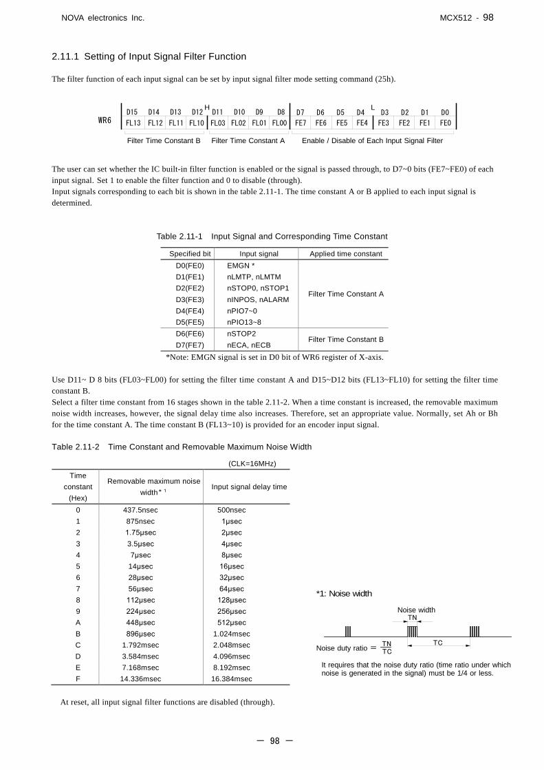
NOVA electronics Inc. MCX512 - 98
- 98 -
2.11.1 Setting of Input Signal Filter Function The filter function of each input signal can be set by input signal filter mode setting command (25h).
The user can set whether the IC built-in filter function is enabled or the signal is passed through, to D7~0 bits (FE7~FE0) of each input signal. Set 1 to enable the filter function and 0 to disable (through). Input signals corresponding to each bit is shown in the table 2.11-1. The time constant A or B applied to each input signal is determined.
Table 2.11-1 Input Signal and Corresponding Time Constant
Specified bit Input signal Applied time constant D0(FE0) EMGN * D1(FE1) nLMTP, nLMTM D2(FE2) nSTOP0, nSTOP1
Filter Time Constant A D3(FE3) nINPOS, nALARM D4(FE4) nPIO7~0 D5(FE5) nPIO13~8 D6(FE6) nSTOP2
Filter Time Constant B D7(FE7) nECA, nECB
*Note: EMGN signal is set in D0 bit of WR6 register of X-axis. Use D11~ D 8 bits (FL03~FL00) for setting the filter time constant A and D15~D12 bits (FL13~FL10) for setting the filter time constant B. Select a filter time constant from 16 stages shown in the table 2.11-2. When a time constant is increased, the removable maximum noise width increases, however, the signal delay time also increases. Therefore, set an appropriate value. Normally, set Ah or Bh for the time constant A. The time constant B (FL13~10) is provided for an encoder input signal.
Table 2.11-2 Time Constant and Removable Maximum Noise Width
(CLK=16MHz) Time
constant (Hex)
Removable maximum noise width*1
Input signal delay time
0 437.5nsec 500nsec 1 875nsec 1μsec 2 1.75μsec 2μsec 3 3.5μsec 4μsec 4 7μsec 8μsec 5 14μsec 16μsec 6 28μsec 32μsec 7 56μsec 64μsec 8 112μsec 128μsec 9 224μsec 256μsec A 448μsec 512μsec B 896μsec 1.024msec C 1.792msec 2.048msec D 3.584msec 4.096msec E 7.168msec 8.192msec F 14.336msec 16.384msec
At reset, all input signal filter functions are disabled (through).
D7 D6 D5 D4H L
D15 D14 D13 D12 D11 D10 D9 D8 D3 D2 D1 D0WR6 FL00FL01FL02 FE7 FE4FE5FE6 FE3 FE1FE2 FE0FL13 FL03FL10FL11FL12
Filter Time Constant B Enable / Disable of Each Input Signal FilterFilter Time Constant A
Noise widthTN
TCNoise duty ratio =
TNTC
*1: Noise width
It requires that the noise duty ratio (time ratio under whichnoise is generated in the signal) must be 1/4 or less.

NOVA electronics Inc. MCX512 - 99
- 99 -
2.11.2 Example of Setting Input Signal Filters For the input signals belong to the filter time constant A, set a 128μsec delay filter to EMGN, XLMTP, XLMTM, XSTOP0, XSTOP1 input signals and set “through” to other input signals. XECA, XECB, XSTOP2 input signals belong to the filter time constant B are “through”.
【Program Example】
// Input/output signal filter mode setting WR6 ← 0807h Write // D15~D12 0000 Filter time constant B Filter delay:500nsec // D11~D8 1000 Filter time constant A Filter delay:128lsec // D7 0 XECA, XECB signal (Filter time constant B):Disables the filter (through) // D6 0 XSTOP2 signal (Filter time constant B):Disables the filter (through) // D5 0 XPIO8-13 signal (Filter time constant A):Disables the filter (through) // D4 0 XPIO0-7 signal (Filter time constant A):Disables the filter (through) // D3 0 XINPOS, XALARM signal (Filter time constant A):Disables the filter (through) // D2 1 XSTOP0,1 signal (Filter time constant A):Enables the filter // D1 1 XLMTP, XLMTM signal (Filter time constant A):Enables the filter // D0 1 EMGN signal (Filter time constant A):Enables the filter WR0 ← 0125h Write

NOVA electronics Inc. MCX512 - 100
- 100 -
2.12 Other Functions
2.12.1 Driving By External Signals
This function is that controls relative position driving and continuous pulse driving not by the commands but by external signals (nEXPP, nEXPM). As the number of motor axis controlled by the system increases, there is a possibility that the CPU cannot handle manual operations appropriately such as JOG feed or teaching mode due to the CPU load. This IC can reduce the host CPU load using driving by external signals. And by inputting an encoder 2-phase signal of a manual pulsar, jog feed will be enabled. nPIO4, 5 signals of general purpose input/output signals are assigned to nEXPP, nEXPM signals. To perform driving by external signals, the following items must be set. ① Set nPIO4, 5 signals to the input by PIO signal setting 1 command (21h). ② Set the driving mode by PIO signal setting 2・Other settings (22h). Function Setting for Driving by External Signals of nPIOm Signal To perform driving by external signals, set nPIO4, 5 signals of general purpose input/output signals to nEXPP, nEXPM input signals for driving by external signals. It sets D11~8 bits of PIO signal setting 1 command (21h).
To use the function of nPIO4 signal as the input signal for driving by external signals (nEXPP), set D9, 8 bits as 0, 0. Similarly, set D11, 10 bits of nPIO5 signal as 0, 0.
Mode setting for driving
This is the mode setting for driving by external signals. It sets D9, 8 bits of PIO signal setting 2・Other settings (22h).
Use 2 bits, D9, 8 bits to set the mode of driving by external signals (nEXPP, nEXPM). The driving mode corresponding to each bit is shown in the table below.
Table 2.12-1 Mode of Driving by External Signals
D9(EXOP1) D8(EXOP0) Mode of driving by external signals 0 0 Disables the driving by external signals 0 1 Continuous pulse driving mode 1 0 Relative position driving mode 1 1 Manual pulsar mode
WR6D7 D6 D5 D4
H LD15 D14 D13 D12 D11 D10 D9 D8 D3 D2 D1 D0
P4M0P5M0 P4M1P5M1
nPIO4 SignalnPIO5 SignalnEXPM nEXPP
WR6D7 D6 D5 D4
H LD15 D14 D13 D12 D11 D10 D9 D8 D3 D2 D1 D0
EXOP0EXOP1
Driving Modeby External Pulses

NOVA electronics Inc. MCX512 - 101
- 101 -
Relative position driving mode Set D9, 8 bits of PIO signal setting 2・Other settings (22h) to 1, 0 and set the appropriate speed parameters for relative position driving and drive pulse number (positive value). Once nEXPP falls down to the Low level (↓), +direction relative position driving will start by ↓ of it. Similarly, once nEXPM falls down to the Low level (↓), -direction relative position driving will start by ↓ of it. The Low level width of each signal must be larger than 4 CLK cycles. Before the driving is finished, if the signal falls down from the Hi to Low level again, it will be invalid.
Fig. 2.12-1 Example of X axis Relative Position Driving (Drive Pulse Number: 5) by External Signal
Continuous Pulse Driving Mode Set D9, 8 bits of PIO signal setting 2・Other settings (22h) to 0, 1 and set the appropriate speed parameters for continuous pulse driving. Once nEXPP falls down to the Low level (↓), the +direction driving pulses will be output continuously during the low level. If nEXPP returns from Low level to Hi level, decelerating stop will be performed in trapezoidal driving and instant stop will be performed in constant speed driving. Similarly, nEXPM will output the -direction driving pulses continuously during the low level. If the other input signal of nEXPP/nEXPM signals falls down from the Hi to Low level, the driving in the other direction will start immediately after the driving in the current direction is finished.
Fig. 2.12-2 Example of X axis Continuous Pulse Driving by External Signal
XEXPP
XEXPM
XPP
XPM
XEXPP
XEXPM
XPP
XPM
Low period
Low period
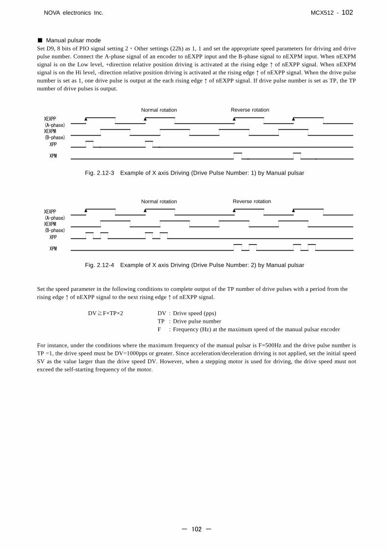
NOVA electronics Inc. MCX512 - 102
- 102 -
Manual pulsar mode Set D9, 8 bits of PIO signal setting 2・Other settings (22h) as 1, 1 and set the appropriate speed parameters for driving and drive pulse number. Connect the A-phase signal of an encoder to nEXPP input and the B-phase signal to nEXPM input. When nEXPM signal is on the Low level, +direction relative position driving is activated at the rising edge ↑ of nEXPP signal. When nEXPM signal is on the Hi level, -direction relative position driving is activated at the rising edge ↑ of nEXPP signal. When the drive pulse number is set as 1, one drive pulse is output at the each rising edge ↑ of nEXPP signal. If drive pulse number is set as TP, the TP number of drive pulses is output.
Fig. 2.12-3 Example of X axis Driving (Drive Pulse Number: 1) by Manual pulsar
Fig. 2.12-4 Example of X axis Driving (Drive Pulse Number: 2) by Manual pulsar
Set the speed parameter in the following conditions to complete output of the TP number of drive pulses with a period from the rising edge ↑ of nEXPP signal to the next rising edge ↑ of nEXPP signal. DV≧F×TP×2 DV :Drive speed (pps) TP :Drive pulse number F :Frequency (Hz) at the maximum speed of the manual pulsar encoder For instance, under the conditions where the maximum frequency of the manual pulsar is F=500Hz and the drive pulse number is TP =1, the drive speed must be DV=1000pps or greater. Since acceleration/deceleration driving is not applied, set the initial speed SV as the value larger than the drive speed DV. However, when a stepping motor is used for driving, the drive speed must not exceed the self-starting frequency of the motor.
XEXPP(A-phase)XEXPM(B-phase)
XPP
XPM
Normal rotation Reverse rotation
Normal rotation Reverse rotation
XEXPP(A-phase)XEXPM(B-phase)
XPP
XPM

NOVA electronics Inc. MCX512 - 103
- 103 -
2.12.2 Pulse Output Type Selection Drive pulse output signals are XPP/PLS/PA (36) and XPM/DIR/PB (37) in X axis, YPP/PLS/PA (38) and YPM/DIR/PB (39) in Y axis. Four pulse output types are available to each axis as shown in the table below. In independent 2-pulse type, when the driving is in the +direction, the pulse output is from nPP, and when the driving is in the -direction, the pulse output is from nPM. In 1-pulse 1- direction type, nPLS is for output of drive pulses and nDIR is for output of direction signals. In quadrature pulse type, the A-phase signal of quadrature pulse is output to nPA and the B-phase signal of quadrature pulse is output to nPB. In quadrature pulse and quad edge evaluation, when output of nPA, nPB pulses changes, the logical position counter is up (down). In quadrature pulse and double edge evaluation, when output of nPA pulses changes, the logical position counter is up (down).
Table 2.12-2 Example of X axis Drive Pulse Output Type
Pulse output type can be set by D4, 3 bits (DPMD1, 0) of WR3 register.
The mode setting for driving corresponding to each bit is as follows.
Table 2.12-3 Drive Pulse Output Type
D4(DPMD1) D3(DPMD0) Pulse Output Type 0 0 Independent 2-pulse 0 1 1-pulse 1-direction 1 0 Quadrature pulse and quad edge evaluation 1 1 Quadrature pulse and double edge evaluation
Please refer to chapter 11.2 for the timing of output pulse signal (nPLS) and direction signal (nDIR) in 1-pulse 1-direction type. When the user wants to set nDIR signal before driving, write direction signal +setting command (58h) or direction signal -setting command (59h). And it sets the logical level of driving pulses by D5 bit (DP-L), the logical level of the direction (DIR) output signal by D6 bit (DIR-L) and sets whether the output pins of a drive pulse signal are replaced or not by D7 bit (DPINV). [Note]
• In interpolation driving, the direction changes on the way, therefore, use independent 2-pulse type for interpolation driving and not 1-pulse 1-direction type.
XPB
XPA
XPB
XPA
XDIR
XPM
XPP
XPLS
Independent 2-pulse
1-pulse 1-direction
Quadrature pulses andquad edge evaluation
Quadrature pulses anddouble edge evaluatio
Pulse Output Type Signal Driving in the + direction Driving in the - direction
0LP 1 2 3 44 3 2 1 0
Pulse OutputType
Drive pulse logicDrive direction signal logicDrive pulse pin inversion
D7 D6 D5 D4H L
D15 D14 D13 D12 D11 D10 D9 D8 D3 D2 D1 D0WR3 DPMD0DPMD1DP-LDIR-LDPINV

NOVA electronics Inc. MCX512 - 104
- 104 -
2.12.3 Encoder Pulse Input Type Selection The encoder pulse input (nECA/PPIN, nECB /PMIN) which counts up/down the real position counter can be selected from 2 types, quadrature pulses input and Up/Down pulse input. Quadrature pulses input As quadrature pulses input types, the user can select from 3 types, quadrature pulses input and quad edge evaluation, quadrature pulses input and double edge evaluation, quadrature pulses input and single edge evaluation. When quadrature pulses input type is engaged and ECA signal goes faster 90 degree phase than ECB signal does, it's "count up" and ECB signal goes faster 90 degree phase than ECA signal does, it's "count down". And when quad edge evaluation is set, it counts Up/Down at the rising edge (↑) and falling edge (↓) of both signals. When double edge evaluation is set, it counts Up/Down at the rising edge (↑) and falling edge (↓) of A-phase signals. When single edge evaluation is set, it counts Up/Down at the rising edge (↑) of A-phase signals.
Fig. 2.12-5 Example of X axis Quadrature Pulse Input
Up/down pulse input
nECA/PPIN is for "count up" input, and nECB/PMIN is for "count down" input. The counter counts up when the positive pulses go up (↑). (when the positive logic is set.)
Fig. 2.12-6 Example of X axis Up / Down Pulse Input
XECA/PPIN
XECB/PMIN
× × × ×
××××××
× × × ×
× ×
××××
Quadrature pulses andquad edge evaluationQuadrature pulses anddouble edge evaluationQuadrature pulses andsingle edge evaluation
:Count up×:Not count up
:Count down×:Not count down
XECA/PPIN
XECB/PMINCount up Count down

NOVA electronics Inc. MCX512 - 105
- 105 -
Encoder Pulse Input Type Setting Encoder pulse input type can be set by D8, 9 bits (PIMD0, 1) of WR3 register.
The encoder pulse input type corresponding to each bit is as follows.
Table 2.12-4 Encoder pulse input type
D9(PIMD1) D8(PIMD0) Encoder pulse input type 0 0 Quadrature pulses input and quad edge evaluation 0 1 Quadrature pulses input and double edge evaluation 1 0 Quadrature pulses input and single edge evaluation 1 1 Up/Down pulse input
And it sets the logical level of an encoder input signal by D10 bit (PI-L) and sets whether the input pins of an encoder pulse input are replaced or not by D11 bit (PIINV). The increase/decrease of the real position counter due to replacing input pins of an encoder input signal as shown in the table below.
Table 2.12-5 Increase/Decrease of Real Position Counter due to Replacing Input Pins of Encoder Input Signal
WR3/D11(PIINV) Pulse input mode Increase/decrease of real position counter
0 quadrature pulses mode
Count UP when the A phase is advancing. Count DOWN when the B phase is advancing.
Up/Down pulse mode Count UP at nPPIN pulse input. Count DOWN at nPMIN pulse input.
1 quadrature pulses mode
Count UP when the B phase is advancing. Count DOWN when the A phase is advancing.
Up/Down pulse mode Count UP at nPMIN pulse input. Count DONW at nPPIN pulse input.
2.12.4 Hardware Limit Signals Hardware limit signals, nLMTP and nLMTM, are used for stopping the pulse output if the limit sensors of +and -directions are triggered. The user can set a limit signal as enable/disable and set the logical level of a limit signal, and set whether to perform decelerating stop or instant stop when a limit signal becomes active, and select whether to replace input pins of hardware limit input signals. Enable/disable of a limit signal, the logical level of a limit signal and the stop type can be set by D12~10 bits of WR2 register. For more details of the WR2 register, see chapter 6.6. Whether to replace input pins of hardware limit input signals or not can be set by D12 bit (LMINV) of WR3 register. For more details of the WR3 register, see chapter 6.7. The status of a limit signal can be read out from RR3 register Page0 anytime.
Encoder pulseinput type
Logical level of encoder input signal
Replacing input pins of encoder input signal
D7 D6 D5 D4H L
D15 D14 D13 D12 D11 D10 D9 D8 D3 D2 D1 D0WR3 PIMD0PIMD1PI-LPIINV

NOVA electronics Inc. MCX512 - 106
- 106 -
2.12.5 Interface to Servo Motor Driver nINPOS signal and nALARM signal As the input signals for connecting a servo motor driver, there are the nINPOS signal (in-position input signal) and the nALARM signal (alarm input signal). The user can set each signal as enable/disable and the logical level by D9~6 bits of WR2 register. For more details of the WR2 register, see chapter 6.6. nINPOS input signal responds to the in-position signal of a servo motor driver. When set to enable, and if nINPOS becomes active after driving is finished, D1~0 bits (n-DRV: Driving status) of RR0 (main status) register will return to 0. nALARM input signal receives the alarm signal from a servo motor driver. When set to enable, it monitors nALARM signal during the driving, and when nALARM becomes active, driving will stop instantly. At this time, D4 (ALARM) and D14 (ALARM) bits of RR2 register become 1. The status of these input signals from a servo motor driver can be read out from RR3 register Page0 anytime. Deviation counter clear output signal A Deviation counter clear signal (nDCC) is available as a servo motor driver output signal. The logical level of a deviation counter clear signal (nDCC) and pulse width can be set by D3~6 bits of automatic home search mode setting 2 command (24h). For more details of the automatic home search mode setting 2 command (24h), see chapter 7.3.5. When deviation counter clear output command (72h) is written, deviation counter clear pulses are output based on the logical level of pulses and pulse width set by automatic home search mode setting 2 command (24h). In the case of using the deviation counter clear signal (nDCC) in automatic home search, see chapter 2.5.2 and 2.5.4. 2.12.6 Emergency Stop MCX512 has the input signal EMGN that can perform the emergency stop function during the driving of all 2 axes. Normally, this signal is kept on the Hi level. When it falls down to the Low level, all axes which drive will stop immediately and D5 (EMG) and D15 (EMG) bits of RR2 register become 1. Please note that there is no way to select the logical level of EMGN signal. There are the following methods to perform the emergency stop to function for 2 axes from the host CPU.
a. Write an instant stop command to 2 axes Specify all 2 axes to WR0 register and then write instant stop command (57h).
b. Write a command reset
Write 00FFh into WR0 register, and it will be reset.

NOVA electronics Inc. MCX512 - 107
- 107 -
2.12.7 Status Output The status of driving/stop is output to D1~0 (n-DRV) bits of RR0 register and nPIO0 signal. The driving status of acceleration/constant speed/deceleration is output to D4 (ASND), D5 (CNST), D6 (DSND) bits of RR3 register Page1 in each axis, and also the signals nPIO2/ASND, nPIO3/CNST, nPIO4/DSND show the levels.
Fig. 2.12-7 Driving Status
Table 2.12-6 RR0, RR3 registers and nPIOm signal corresponding to Driving Status
Drive Status RR0 register RR3 register Page1 nPIOm signal D3~0(n-DRV) D4/ASND D5/CNST D6/DSND nPIO0/DRIVE nPIO2/ASND nPIO3/CNST nPIO4/DSND
Stop 0 0 0 0 Low Low Low Low Acceleration 1 1 0 0 Hi Hi Low Low
Constant Speed 1 0 1 0 Hi Low Hi Low Deceleration 1 0 0 1 Hi Low Low Hi
In S-curve acceleration/deceleration driving, the status of increasing/constant/decreasing of acceleration and deceleration is output to D7(AASND), D8(ACNST), D9(ADSND) bits of RR3 register Page1 in each axis and nPIO5/AASND, nPIO6/ACNST, nPIO7/ADSND signals. To output the driving status to nPIOm signal, use PIO signal setting 1 command (21h). See chapter 7.3.2
Stop AccelerationConstantSpeed Deceleration Stop
Speed
Time
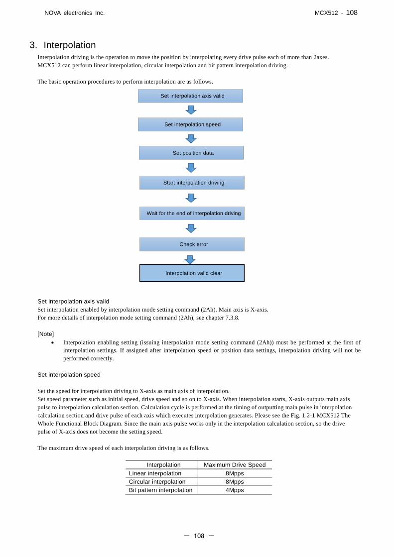
NOVA electronics Inc. MCX512 - 108
- 108 -
3. Interpolation Interpolation driving is the operation to move the position by interpolating every drive pulse each of more than 2axes. MCX512 can perform linear interpolation, circular interpolation and bit pattern interpolation driving. The basic operation procedures to perform interpolation are as follows.
Set interpolation axis valid Set interpolation enabled by interpolation mode setting command (2Ah). Main axis is X-axis. For more details of interpolation mode setting command (2Ah), see chapter 7.3.8. [Note]
• Interpolation enabling setting (issuing interpolation mode setting command (2Ah)) must be performed at the first of interpolation settings. If assigned after interpolation speed or position data settings, interpolation driving will not be performed correctly.
Set interpolation speed
Set the speed for interpolation driving to X-axis as main axis of interpolation. Set speed parameter such as initial speed, drive speed and so on to X-axis. When interpolation starts, X-axis outputs main axis pulse to interpolation calculation section. Calculation cycle is performed at the timing of outputting main pulse in interpolation calculation section and drive pulse of each axis which executes interpolation generates. Please see the Fig. 1.2-1 MCX512 The Whole Functional Block Diagram. Since the main axis pulse works only in the interpolation calculation section, so the drive pulse of X-axis does not become the setting speed. The maximum drive speed of each interpolation driving is as follows.
Interpolation Maximum Drive Speed Linear interpolation 8Mpps Circular interpolation 8Mpps Bit pattern interpolation 4Mpps
Set interpolation speed
Set position data
Start interpolation driving
Set interpolation axis valid
Wait for the end of interpolation driving
Check error
Interpolation valid clear

NOVA electronics Inc. MCX512 - 109
- 109 -
Be sure to set interpolation speed when interpolation driving is performed, especially in the following cases, it must be set. • When interpolation driving is performed after normal driving, and when speed parameters are the same as those in normal
driving. • After interpolation driving, when interpolation driving is performed without changing speed and position parameters but
interpolation mode setting is changed.
Speed changing during interpolation driving Speed can be changed during interpolation driving by synchronous action. To change speed, set speed which the user want to change to the multi-purpose register. For synchronous action, see chapter 2.6.
[Note] When setting to short axis pulse equalization mode, set 8 times value of which the user want to perform. For example, when the user want to perform by 1000pps, set [8000]. The value can be set within [1~8,000,000].
Set position data In linear interpolation, set the finish point of each axis, and in circular interpolation, set the center and finish points of a circular arc. In bit pattern interpolation, set the bit data in the +/- direction of each axis. In bit pattern interpolation, the user can write 128 bit data to each axis before interpolation driving starts.
[Note] • Even though interpolation driving that has the same position data is performed continuously, be sure to set position data.
Start interpolation driving After necessary speed and position parameters for interpolation are set, if interpolation driving command is written, interpolation driving will start. In bit pattern interpolation, the user can infinitely draw an arbitrary drive locus continuously by filling bit data during interpolation driving. Wait for termination of interpolation driving During interpolation driving, n-DRV bits of all axes that perform RR0 (main status register) interpolation become 1. And after interpolation driving is finished, the bits return to 0. Error check During interpolation driving, hardware and software limit error works in each driving axis. When the limit of any axis becomes active during interpolation driving, the interpolation stops. If stopped by an error, the error bit of the axis designated interpolation in RR0 (main status register) will become 1. If the bit is 1, the user can identify the cause of the error by reading RR2 (error register) of the axis. [Note]
• In circular and bit pattern interpolation, the hardware or software limit of either +/-direction becomes active, the interpolation may stop. In this case, the user cannot escape from the limit area by circular and bit pattern interpolation. Please escape it by driving the axis alone.
Interpolation valid clear When interpolation driving is finished, be sure to clear the specification of interpolation valid by interpolation mode setting command (2Ah). If normal driving is performed with interpolation valid, driving may not be performed correctly. In-position Signal for Servo Motor During interpolation driving, in case of the in-position signal (nINP0S) of each axis being enabled, nINP0S signals of all axes become active after interpolation driving is finished, and then the drive bits of all axes that perform RR0 (main status register) interpolation return to 0.
Stop of interpolation driving by synchronous action
When interpolation driving is stopped by synchronous action, be sure to write error/finishing status clear command (79h) into the interpolation axis after checking that interpolation drive stops. The user can check the termination of driving by synchronous action, by using D8 bit of RR2 register. For more details of synchronous action, see chapter 2.6, and details of RR2 register, see chapter 6.13.

NOVA electronics Inc. MCX512 - 110
- 110 -
Interpolation driving after driving stops by nSTOP0, nSTOP1 or nSTOP2 signal When interpolation driving is performed by using the stopped axis after the driving except interpolation is stopped by nSTOP0, nSTOP1 or nSTOP2 signal, be sure to write error/finishing status clear command (79h) into the interpolation axis. The user can check the termination of driving by RR2 register. For more details of RR2 register, see chapter 6.13.

NOVA electronics Inc. MCX512 - 111
- 111 -
3.1 2-axis Linear Interpolation
2 axes can be set for linear interpolation. To execute linear interpolation, set the finish point coordinates relative to the present point coordinates, and write the linear interpolation driving command based on the number of interpolation axis, then linear interpolation will be performed. The finish point coordinates should be set to output pulse number of each axis by the relative value to the present point coordinates. Fig. 3.1-1 shows 2-axis interpolation where linear interpolation is performed from the current coordinates to the finish point coordinates. As shown in the figure, the calculation accuracy of position to the ideal line is within ±0.5 LSB. As shown in Fig. 3.1-2, it is an example for pulse output of the linear interpolation driving. We define the longest distance movement in interpolation is the “long axis”. And the other is “short axis”. The long axis outputs an average pulse train. The driving pulse of the short axis depends on the long axis and the relationship of the two axes. When constant vector speed mode is disabled, the speed of the drive pulse in long axis becomes the drive speed for the main axis. The range for each axis is a 32-bit signed counter, from -2,147,483,646~+2,147,483,646 (signed 32-bit-2LSB). 3.1.1 Maximum Finish Point The absolute value of the finish point in long axis is called the maximum finish point. At the reset initial state of IC, the maximum finish point is automatically calculated, but the user can set it manually by interpolation mode setting command (2Ah). If in manual setting, the user can specify the arbitrary value as the maximum finish point. For more details of interpolation mode setting command (2Ah), see chapter 7.3.8.
Fig. 3.1-1 Position Accuracy for Linear Interpolation
Fig. 3.1-2 Example of Pulse Output at Finish Point (X=20, Y=9)
5 10 15 20
5
(20,9)
0
Y
±0.5 LSB max
XLong axis
Short axis
XPPXPMYPPYPM
Long axis
Short axis

NOVA electronics Inc. MCX512 - 112
- 112 -
3.1.2 Examples of Linear Interpolation for 2 axes
Example of linear interpolation for 2 axes
Executes linear interpolation in X and Y axes from the current position to the finish position (X: +30000, Y: -20000). The interpolation drive speed is initial speed: 500PPS, acceleration/deceleration: 40,000PPS/SEC and drive speed: 5,000PPS.
. WR6 ← 0001h Write ;interpolation axis X, Y WR0 ← 002Ah Write WR6 ← 9C40h Write ;40,000 PPS/SEC WR7 ← 0000h Write
WR0 ← 0102h Write ;Set acceleration to main axis.
WR6 ← 01F4h Write ;500 PPS WR7 ← 0000h Write
WR0 ← 0104h Write ;Set initial speed to main axis.
WR6 ← 1388h Write ;5000 PPS WR7 ← 0000h Write
WR0 ← 0105h Write ;Set drive speed to main axis.
WR6 ← 7530h Write ;Finish point X :30,000 WR7 ← 0000h Write WR0 ← 0106h Write
WR6 ← B1E0h Write ;Finish point Y :-20,000 WR7 ← FFFFh Write WR0 ← 0206h Write WR0 ← 006Dh Write ;Deceleration valid WR0 ← 0061h Write ;2-axis linear interpolation drive
10000 20000 30000
-10000
-20000
XY
(30000, -20000)
0

NOVA electronics Inc. MCX512 - 113
- 113 -
3.2 Circular Interpolation
Executes 2 axes of X and Y-axis circular interpolation driving. In the orthogonal coordinates in the right figure, X-axis is set to ax1 axis (horizontal axis), Y-axis is set to ax2 axis (vertical axis). The right direction of ax1 (horizontal axis) is +direction, and the upper direction of ax2 (vertical axis) is +direction. The user can reverse the axes by interpolation mode setting. To execute circular interpolation, set the center point coordinates of a circular arc and the finish point coordinates relative to the present point coordinates (start point), and write CW or CCW circular interpolation driving command, then circular interpolation will be performed. The center and finish point coordinates must be set by the relative value to the present point coordinates. In Fig. 3.2-1 CW/CCW circular interpolation, it explains the definition of CW and CCW circular interpolations. The CW circular interpolation is starting from the start point to the finish point in clockwise direction; the CCW circular interpolation is in counter-clockwise direction. When the finish point is set to (0, 0), a full circle will come out. In Fig. 3.2-2, it explains the long axis and short axis. We define 8 quadrants in the X-Y plane and put the number 0~7 to each quadrant. As shown in the figure, the absolute value of ax1 is always larger than that of ax2 in quadrants 0, 3, 4 and 7, and it is defined ax1 is the long axis and ax2 is the short axis in these quadrants. In quadrants 1, 2, 5 and 6, ax2 is the long axis and ax1 is the short axis. The short axis outputs pulses regularly, and the long axis outputs or does not output pulses depending on the interpolation calculation. In Fig. 3.2-3, it is an example to generate a full circle of radius 11 with the center point (-11, 0) and the finish point (0, 0). And Fig. 3.2-4 shows the pulse output at that time.
The range of the center and finish point coordinates is -2,147,483,646~+2,147,483,646 from the current position. The position tolerance for the specified circular curve is ±1 LSB within the entire interpolation range. The interpolation speed is within the range from 1PPS to 8MPPS.
0
12
3
4
5 6
7
ax1
ax2
ax2
ax2
ax2
ax2
ax1 ax1
ax1 ax1
X
Y
track of interpolationsolid line: circle with radium 11dash line: circle with radium 11 1
start point / finish point
0
12
3
4
5 6
7
CCW(ax1, ax2)
Fig. 3.2-1 CW/CCW circular interpolation
Fig. 3.2-2 The 0~7 Quadrants And Short Axis Fig. 3.2-3 Example of CircularInterpolation
Fig. 3.2-4 Example of Pulse Output in Circular Interpolation Driving
ax1
ax2
Center pointFinish point
Finish point
CCW circular interpolation
CW circular interpolation
Start point
Start point
XPP
XPMYPP
YPM10 2 3 4 5 6 7Quadrant

NOVA electronics Inc. MCX512 - 114
- 114 -
3.2.1 The Finish Point Checking of Circular Interpolation In the circular interpolation, it assumes that the current position (start point) is (0, 0). The radius is determined depending on the value of the center point coordinates, and then the circular tracking will start. The maximum error range of interpolation is within ±1LSB. Because of the ±1LSB error range, the designated finish point may not on the circular track. When the current point is same or over the finish point of short axis, this circular interpolation is finished in the quadrant where the finish point is. If the current point cannot reach the finish point of short axis, this circular interpolation is finished in the end of the quadrant where the current point reaches. Fig. 3.2-5 shows an example of CCW interpolation with the start point (0, 0), center point (-200,500) and finish point (-702, 299). The finish point is in quadrant 4, and ax2 is the short axis in quadrant 4. So the interpolation is finished when the ax2 is 299. 3.2.2 Toggle of Interpolation Axis The interpolation axes are defined that X-axis is set to ax1 (horizontal axis) and Y-axis is set to ax2 (vertical axis) in circular interpolation driving. However, the user can toggle between the two axes. When the user wants to change Y-axis to ax1 (horizontal axis) and X-axis to ax2 (vertical axis), set D4 bit of WR6 register to 1 by interpolation mode setting command (2Ah).
3.2.3 The Example for CW Circular Interpolation
This CW circular interpolation starts from the current point (start point: 0, 0) to the finish point (X: 5000, Y: -5000); the center point is X: 5000, Y: 0. The interpolating speed is constant at 1000PPS in 2-axis simple constant vector speed driving. WR6 ← 0041h Write ;define: ax1:X axis, ax2:Y axis, and with 2-axis simple constant linear speed WR0 ← 002Ah Write WR6 ← 03E8h Write ;1000 PPS WR7 ← 0000h Write WR0 ← 0104h Write ;Set initial speed to main axis WR6 ← 03E8h Write ;1000 PPS WR7 ← 0000h Write WR0 ← 0105h Write ;Set drive speed to main axis WR6 ← 1388h Write ;center point of X:5000 WR7 ← 0000h Write WR0 ← 0108h Write WR6 ← 0000h Write ;center point of Y:0 WR7 ← 0000h Write WR0 ← 0208h Write WR6 ← 1388h Write ;finish point of X:5000 WR7 ← 0000h Write WR0 ← 0106h Write WR6 ← EC78h Write ;finish point of Y:-5000 WR7 ← FFFFh Write WR0 ← 0206h Write WR0 ← 0064h Write ;CW circular interpolation driving
Fig. 3.2-5 CW/CCW Circular Interpolation
Start point (0,0)
Center point(-200,500)
Finish point(-702,299)
ax2
ax1
Interpolation will be finishedwhen ax2=299 in the 4thquadrant.
0
12
3
4
6
7
Start point(0,0)
Center point(5000,0)
Finish point (5000,-5000)
X
Y

NOVA electronics Inc. MCX512 - 115
- 115 -
3.3 2 axes Bit Pattern Interpolation MCX512 bit pattern interpolation is the operation that performs interpolation of two axes by specifying whether to output pulses in the + or -direction by a unit of 1 drive pulse.
The user sets drive pulse in the + or -direction by one bit one pulse from the CPU to each interpolation axis, 1 is to output and 0 is not to output. For example, to draw the profile as shown in the right Fig. 3.4-1, if output of drive pulse each in X+, X-, Y+, Y- direction is “1”, and no output is “0”, the bit pattern data is as follows.
Fig. 3.3-1 Example of Bit Pattern Interpolation
The operation procedures to perform bit pattern interpolation are as follows.
Fig. 3.3-2 Operation Procedures for Bit Pattern Interpolation
64 48 32 16 010010111 11111111 11111110 10000000 00000000 00000000 00000011 11111111 11111111 11100100 :XPP(X+direction pulse)10000000 00000000 00000000 00001111 11111111 11111111 01000000 00000000 00000000 00000000 :XPM(X-direction pulse)00000000 00000000 00011111 11111111 01001010 10101011 11111111 11010000 00000000 00000000 :YPP(Y+direction pulse)01111111 00100000 00000000 00000000 00000000 00000000 00000000 00000000 00000011 11111111 :YPM(Y-direction pulse)
79
Set interpolation speed
Write bit pattern data
Write interpolation driving command
Set interpolation axis valid
Is full pre-buffer?
Interpolation data finished?
Yes
No
Yes
No
Finished
X+
Y+
0
16
32
48
64
79
Start point
Finish point
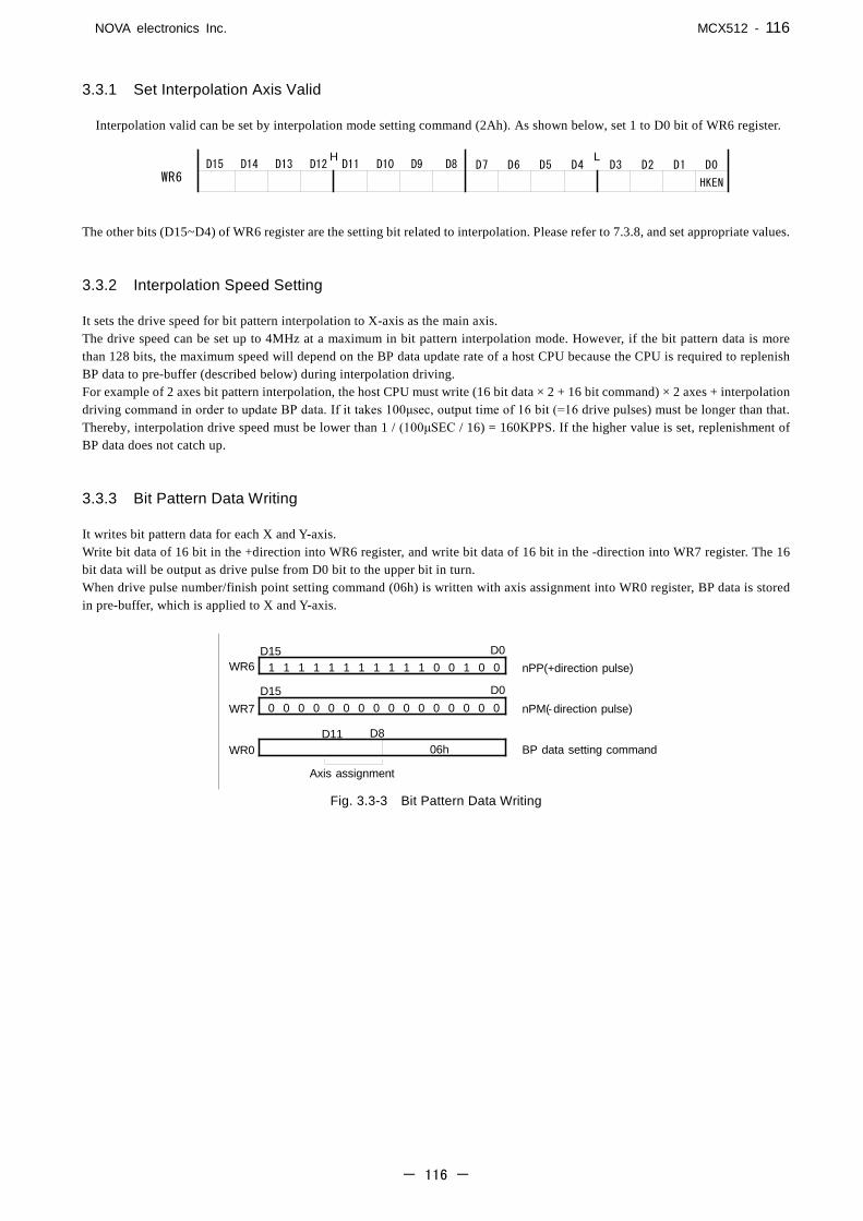
NOVA electronics Inc. MCX512 - 116
- 116 -
3.3.1 Set Interpolation Axis Valid
Interpolation valid can be set by interpolation mode setting command (2Ah). As shown below, set 1 to D0 bit of WR6 register.
The other bits (D15~D4) of WR6 register are the setting bit related to interpolation. Please refer to 7.3.8, and set appropriate values. 3.3.2 Interpolation Speed Setting It sets the drive speed for bit pattern interpolation to X-axis as the main axis. The drive speed can be set up to 4MHz at a maximum in bit pattern interpolation mode. However, if the bit pattern data is more than 128 bits, the maximum speed will depend on the BP data update rate of a host CPU because the CPU is required to replenish BP data to pre-buffer (described below) during interpolation driving. For example of 2 axes bit pattern interpolation, the host CPU must write (16 bit data × 2 + 16 bit command) × 2 axes + interpolation driving command in order to update BP data. If it takes 100μsec, output time of 16 bit (=16 drive pulses) must be longer than that. Thereby, interpolation drive speed must be lower than 1 / (100μSEC / 16) = 160KPPS. If the higher value is set, replenishment of BP data does not catch up.
3.3.3 Bit Pattern Data Writing It writes bit pattern data for each X and Y-axis. Write bit data of 16 bit in the +direction into WR6 register, and write bit data of 16 bit in the -direction into WR7 register. The 16 bit data will be output as drive pulse from D0 bit to the upper bit in turn. When drive pulse number/finish point setting command (06h) is written with axis assignment into WR0 register, BP data is stored in pre-buffer, which is applied to X and Y-axis.
Fig. 3.3-3 Bit Pattern Data Writing
D7 D6 D5 D4H L
D15 D14 D13 D12 D11 D10 D9 D8 D3 D2 D1 D0WR6 HKEN
WR6
WR7
nPP(+direction pulse)1 1 1 1 1 1 1 1 1 1 1 0 0 1 0 0
0 0 0 0 0 0 0 0 0 0 0 0 0 0 0 0
D15 D0
D15 D0
WR0
nPM(-direction pulse)
06hD8D11
Axis assignment
BP data setting command
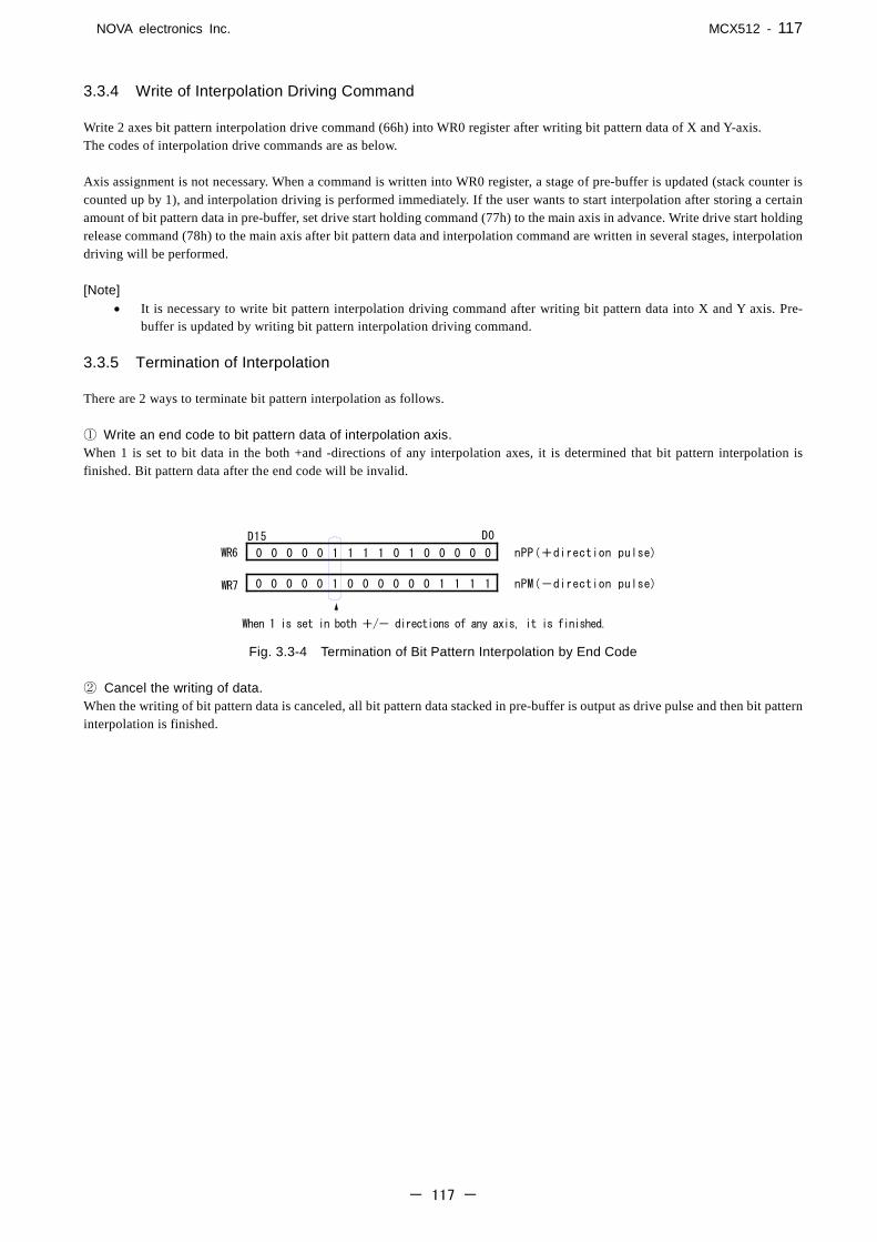
NOVA electronics Inc. MCX512 - 117
- 117 -
3.3.4 Write of Interpolation Driving Command Write 2 axes bit pattern interpolation drive command (66h) into WR0 register after writing bit pattern data of X and Y-axis. The codes of interpolation drive commands are as below.
Axis assignment is not necessary. When a command is written into WR0 register, a stage of pre-buffer is updated (stack counter is counted up by 1), and interpolation driving is performed immediately. If the user wants to start interpolation after storing a certain amount of bit pattern data in pre-buffer, set drive start holding command (77h) to the main axis in advance. Write drive start holding release command (78h) to the main axis after bit pattern data and interpolation command are written in several stages, interpolation driving will be performed. [Note]
• It is necessary to write bit pattern interpolation driving command after writing bit pattern data into X and Y axis. Pre-buffer is updated by writing bit pattern interpolation driving command.
3.3.5 Termination of Interpolation There are 2 ways to terminate bit pattern interpolation as follows. ① Write an end code to bit pattern data of interpolation axis. When 1 is set to bit data in the both +and -directions of any interpolation axes, it is determined that bit pattern interpolation is finished. Bit pattern data after the end code will be invalid.
Fig. 3.3-4 Termination of Bit Pattern Interpolation by End Code
② Cancel the writing of data. When the writing of bit pattern data is canceled, all bit pattern data stacked in pre-buffer is output as drive pulse and then bit pattern interpolation is finished.
WR6
WR7
When 1 is set in both +/- directions of any axis, it is finished.
nPP(+direction pulse)
nPM(-direction pulse)
0 0 0 0 0 1 1 1 1 0 1 0 0 0 0 0
0 0 0 0 0 1 0 0 0 0 0 0 1 1 1 1
D15 D0
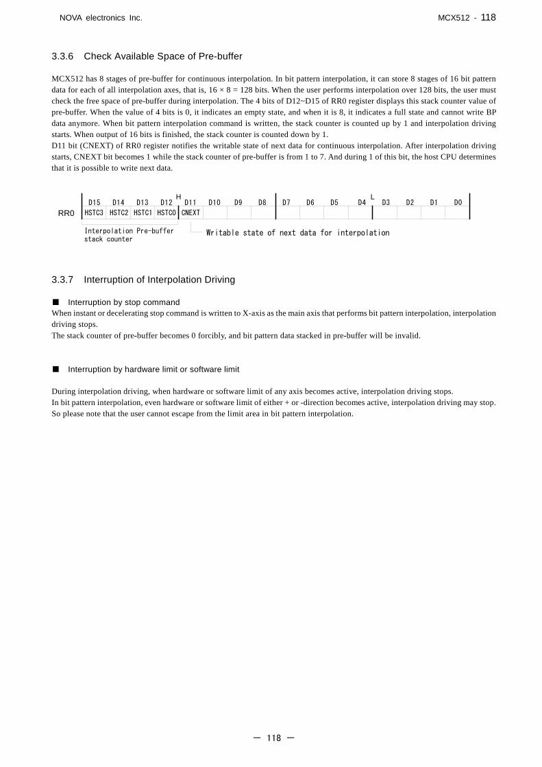
NOVA electronics Inc. MCX512 - 118
- 118 -
3.3.6 Check Available Space of Pre-buffer MCX512 has 8 stages of pre-buffer for continuous interpolation. In bit pattern interpolation, it can store 8 stages of 16 bit pattern data for each of all interpolation axes, that is, 16 × 8 = 128 bits. When the user performs interpolation over 128 bits, the user must check the free space of pre-buffer during interpolation. The 4 bits of D12~D15 of RR0 register displays this stack counter value of pre-buffer. When the value of 4 bits is 0, it indicates an empty state, and when it is 8, it indicates a full state and cannot write BP data anymore. When bit pattern interpolation command is written, the stack counter is counted up by 1 and interpolation driving starts. When output of 16 bits is finished, the stack counter is counted down by 1. D11 bit (CNEXT) of RR0 register notifies the writable state of next data for continuous interpolation. After interpolation driving starts, CNEXT bit becomes 1 while the stack counter of pre-buffer is from 1 to 7. And during 1 of this bit, the host CPU determines that it is possible to write next data.
3.3.7 Interruption of Interpolation Driving
Interruption by stop command When instant or decelerating stop command is written to X-axis as the main axis that performs bit pattern interpolation, interpolation driving stops. The stack counter of pre-buffer becomes 0 forcibly, and bit pattern data stacked in pre-buffer will be invalid.
Interruption by hardware limit or software limit During interpolation driving, when hardware or software limit of any axis becomes active, interpolation driving stops. In bit pattern interpolation, even hardware or software limit of either + or -direction becomes active, interpolation driving may stop. So please note that the user cannot escape from the limit area in bit pattern interpolation.
RR0D15 D14 D13 D12 D11 D10 D9 D8 D7 D6 D5 D4 D3 D2 D1 D0
H L
HSTC0HSTC2HSTC3 HSTC1 CNEXT
Writable state of next data for interpolationInterpolation Pre-bufferstack counter

NOVA electronics Inc. MCX512 - 119
- 119 -
3.3.8 Example of Bit Pattern Interpolation It performs bit pattern interpolation of m×16 bits with X and Y axes. For example, in case of Fig. 3.4-1 Example of Bit Pattern Interpolation, it has 79 bits and so m = 5. Set interpolation drive speed: 1000PPS at constant speed and 2-axis simple constant vector speed mode. The main axis is X-axis, so set drive speed to X-axis. Set drive speed to X-axis as the main axis.
Bit pattern data should be stored in a memory as shown in the table below.
m = 5 m = 4 m = 3 m = 2 m = 1 X axis +direction data X_PlusBPdata(m)
1001011111111111 97FFh
1111111010000000 FE80h
0000000000000000 0000h
0000001111111111 03FFh
1111111111100100 FFE4h
X axis -direction data X_MinusBPdata(m)
1000000000000000 8000h
0000000000001111 000Fh
1111111111111111 FFFFh
0100000000000000 4000h
0000000000000000 0000h
Y axis +direction data Y_PlusBPdata(m)
0000000000000000 0000h
0001111111111111 1FFFh
0100101010101011 4AABh
1111111111010000 FFD0h
0000000000000000 0000h
Y axis -direction data Y_MinusBPdata(m)
0111111100100000 7F20h
0000000000000000 0000h
0000000000000000 0000h
0000000000000000 0000h
0000001111111111 03FFh
WR6 ← 0041h Write ;X axis and Y axis, 2-axis simple constant vector speed mode WR0 ← 002Ah Write ;Set interpolation mode WR6 ← 03E8h Write ;X axis (main axis) Set speed parameters WR7 ← 0000h Write ;Initial speed:1000 PPS WR0 ← 0104h Write WR6 ← 03E8h Write ;Drive speed:1000 PPS WR7 ← 0000h Write WR0 ← 0105h Write
m ← ;Data pointer =1 Loop: WR6 ← X_PlusBPdata(m) Write ;X axis +direction BP data WR7 ← X_MinusBPdata(m) Write ;X axis -direction BP data
WR0 ← 0106h Write
WR6 ← Y_PlusBPdata(m) Write ;Y axis +direction BP data WR7 ← Y_MinusBPdata(m) Write ;Y axis -direction BP data
WR0 ← 0206h Write WR0 ← 0066h Write ;2-axis BP interpolation command ;Starts interpolation driving by the first execution of this step m ← + 1 ;Data pointer is incremented ;If m = 6, it is terminated. RR0 → RR0, it is terminated ;Checks free space of pre-buffer ;If RR0/D11 = 1, jump to Loop, and if = 0, go to RR0 Read
Bit pattern interpolation by interrupt The interrupt signal (INT1N) for continuous interpolation is provided. This signal becomes active (Low level) when the stack counter of pre-buffer changes from 8 to 7 or from 4 to 3. After the interrupt signal is generated, the host CPU can write the next BP data until the stack counter becomes 8 (while CNEXT bit is 1). It means that the host CPU can write the next BP data of 1 stage when selected from 8 to 7, and 5 stages continuously when selected from 4 to 3. The interrupt signal (INT1N) will return to inactive by writing interpolation command (such as bit pattern interpolation command) after BP data is written. And it will return to inactive forcibly when interpolation driving is finished.

NOVA electronics Inc. MCX512 - 120
- 120 -
3.4 Constant Vector Speed
Vector speed is the driving speed of the tip of a locus performing interpolation driving, and it is also called Head speed. In operations such as machining or coating workpieces during interpolation driving, it is important to keep this vector speed constant. MCX512 provides 2-axis simple constant vector speed mode and 2-axis high accuracy constant vector speed mode for 2-axis interpolation. Fig. 3.4-1 shows the locus of 2 axes interpolation in the orthogonal XY plane. Each axis outputs drive pulses according to the basic pulse of the main axis. And as shown in the figure, when both axes output drive pulses, it moves 1.414 times longer distance than that of 1-axis output. If not using constant vector speed mode when both axes outputs drive pulses, the speed will be 1.414 times faster even though the driving distance is 1.414 times longer.
Fig. 3.4-1 Example of 2-axis Interpolation Fig. 3.4-2 shows the speed deviation of vector speed within the range from 0 to 90 degrees of the angle between X axis and the line to be interpolated when linear interpolation is performed in the orthogonal XY plane. Although the figure shows the range 0-90 degrees, the range 90-180, 180-270, 270-360 are the same.
a. Constant vector speed: disabled b. 2-axis simple constant vector speed c. 2-axis high accuracy constant vector speed
Fig. 3.4-2 Speed Deviation of Vector Speed with respect to Setting Speed in Linear Interpolation Driving Fig. 3.4-2 a. is the speed deviation of vector speed with respect to the setting drive speed when constant vector speed mode is disabled. When the angle from X axis is 45 degrees, the speed deviation will be maximum and the speed will increase by approximately +41%. Fig. 3.4-2 b. is the speed deviation in 2-axis simple constant vector speed mode, where the speed deviation is improved by setting 1/1.414 times pulse cycle for both axes pulse output. Fig. 3.4-2 c. is the speed deviation in 2-axis high accuracy constant vector speed mode, where the speed deviation can be kept ±0.2%*1 or less in the range of all angles. *1:Short axis pulse equalization mode must be enabled.
Y
X
Speed becomes1.414 times faster.
0 45 90
+10
+20
+30
+40
Speed Deviation(%)
0
-10 -10
the maximum +41%
the maximum -7.6%
0 45 90
0 45 90
the maximum ±0.2%+10
-10
Angle(°)
+10
Speed Deviation(%)
Speed Deviation(%)
Angle(°) Angle
(°)0 0
Y
X
θAngle(°)
Deviation of resultant speed
Enable short axis pulse equalization mode

NOVA electronics Inc. MCX512 - 121
- 121 -
3.4.1 Constant Vector Speed Setting Constant vector speed can be set by 2 bits, D6 and D7 of interpolation mode setting command (2Ah).
The settings of D6 and D7 bits corresponding to each constant vector speed mode are as follows.
Table 3.4-1 Settings of Constant Vector Speed Mode
D7(SPD1) Bit D6(SPD0) Bit Constant Vector Speed Mode 0 0 Invalid 0 1 2-axis simple constant vector speed 1 1 2-axis high accuracy constant vector speed
Example of linear interpolation in 2-axis high accuracy constant vector speed mode
It performs linear interpolation of X and Y axes with drive speed: 1000PPS at constant speed in 2-axis high accuracy constant vector speed mode, and short axis pulse equalization mode is enabled.
// Set interpolation mode WR6 ← 01C1h Write // XY axes interpolation, 2-axis high accuracy constant vector speed mode, // Short axis pulse equalization mode enabling WR0 ← 002Ah Write // Interpolation mode setting command
// Set drive speed to main axis WR6 ← 03E8h Write // Initial speed:1000pps WR7 ← 0000h Write WR0 ← 0104h Write
WR6 ← 03E8h Write // Drive speed:1000pps WR7 ← 0000h Write WR0 ← 0105h Write
// Set Finish point WR6 ← 03E8h Write // Finish point X:1000 WR7 ← 0000h Write WR0 ← 0106h Write
WR6 ← 0190h Write // Finish point Y:400 WR7 ← 0000h Write WR0 ← 0206h Write
// Start interpolation driving WR0 ← 0061h Write // 2-axis linear interpolation driving
D7 D6 D5 D4H L
D15 D14 D13 D12 D11 D10 D9 D8 D3 D2 D1 D0WR6 SPD0SPD1

NOVA electronics Inc. MCX512 - 122
- 122 -
3.5 Short Axis Pulse Equalization
Usually in interpolation driving, all of axes that perform interpolation do not output drive pulses at regular intervals during driving. As shown in Fig. 3.5-1 a. below, in 2-axis linear interpolation, the axis (long axis) that has longer moving distance (pulse) outputs pulses continuously; however, the axis (short axis) that has shorter one sometimes outputs and sometimes does not output pulses depending on the result of interpolation calculation. In a stepper motor, these uneven pulses may increase mechanical vibration. Short axis pulse equalization mode is the function to improve this problem. Even in the axis has shorter moving distance, it can output drive pulses as equal as possible. The following Fig. 3.5-1 b. shows the waveform of the output pulse when short axis pulse equalization mode is enabled.
Fig. 3.5-1 Pulse Waveform in 2-axis Linear Interpolation (Finish point X: 30, Y: 26) Short axis pulse equalization performs the interpolation calculation in the IC, enhancing by several times than usual. Because of that, the setting range of parameters is restricted by 1/8 as shown in the table below. When enabling short axis pulse equalization mode, be sure to perform interpolation driving within the range of the following table.
Table 3.5-1 Setting Range of Parameters in Short Axis Pulse Equalization
Parameter Symbol Settable Range Short axis pulse equalization:
Enabled Usual
Drive speed DV 1~1,000,000 1~8,000,000 Initial speed SV 1~1,000,000 1~8,000,000 Acceleration/Deceleration
AC, DC 1~67,108,863 1~536,870,911
Finish point TP -268,435,455~+268,435,455 -2,147,483,646~+2,147,483,646 Center point of arc CP -268,435,455~+268,435,455 -2,147,483,646~+2,147,483,646
3.5.1 Short Axis Pulse Equalization Setting Short axis pulse equalization can be set by D8 bit of interpolation mode setting command (2Ah).
When 1 is set, short axis pulse equalization is enabled, and when 0 is set, it is disabled.
D7 D6 D5 D4H L
D15 D14 D13 D12 D11 D10 D9 D8 D3 D2 D1 D0WR6 LMDF
1 30
26
30
26
a.Waveform in normal
X
Y1
X
Y
1
1
b.Waveform in short axis pulse equalization mode

NOVA electronics Inc. MCX512 - 123
- 123 -
3.5.2 Notes on Using Short Axis Pulse Equalization
• Short axis pulse equalization cannot be used in the following driving. ① S-curve acceleration/deceleration driving ② Single step interpolation ③ BP interpolation
• When short axis pulse equalization is used in circular interpolation, and if the start and finish points of a circular arc
are not on the X or Y axis, the finish points of both axes may deviate by ±1 pulse. For this reason, in this case the user needs to fully consider whether this deviation will be a problem or not. When the start and finish points of a circular arc are on the X or Y axis, this deviation does not occur.

NOVA electronics Inc. MCX512 - 124
- 124 -
3.6 Continuous Interpolation
Continuous interpolation is the operation that performs a series of interpolation processes such as linear interpolation → circular interpolation → linear interpolation → ···. This can only be performed when the number of the axis that executes continuous interpolation is the same, and it is possible to perform continuous interpolation as shown in the table below.
Table 3.6-1 Executable Continuous Interpolation
Executable Continuous Interpolation Operation Continuance of 2-axis linear interpolation 2-axis linear → 2-axis linear → 2-axis linear → ・・・・・・ Continuance of 2-axis linear interpolation and circular interpolation
2-axis linear → Circular → 2-axis linear →2-axis linear → Circular → ・・・・
Continuous interpolation is achieved by pre-buffer. Before starting interpolation or during interpolation driving, set interpolation data to pre-buffer, and continuous interpolation driving will be performed. The user can set interpolation data of 8 segments to pre-buffer at a maximum.

NOVA electronics Inc. MCX512 - 125
- 125 -
3.6.1 How to Perform Continuous Interpolation To perform continuous interpolation, set interpolation data to pre-buffer in advance and then start interpolation driving. The user can set interpolation data of 8 segments to pre-buffer at a maximum before starting interpolation. After starting interpolation, MCX512 achieves continuous interpolation by setting next interpolation data (segment data) to pre-buffer while checking the value of the stack counter. The operation procedures to perform continuous interpolation are as follows.
Fig. 3.6-1 The Flow of Continuous Interpolation
Set interpolation speed
Write Drive start holding command
Write the 1st segment data・ interpolation command
Set interpolation axis valid
Interpolation finished?
No
Yes
(1)
Write the 8th segment data・ interpolation command
Write Drive start holding release command
Next data writable?
Error occurred?
Write the n segment data・ interpolation command
(2)
(3)
(4)
(5)
Error handling
Finished
Yes
Yes
(6)
(7)
(8)
(9)
(10)

NOVA electronics Inc. MCX512 - 126
- 126 -
(1) Interpolation Axis Valid Setting Interpolation valid can be set by interpolation mode setting command (2Ah). As shown below, to make interpolation valid, set 1 to D0 bit of WR6 register.
・ After starting interpolation, interpolation valid setting cannot be changed. ・ The other bits (D15~D4) of WR6 register are the setting bit related to interpolation. Please refer to 7.3.8, and set
appropriate values. (2) Interpolation Speed Setting It sets the drive speed for interpolation to X-axis as the main axis. The drive speed can be set up to 4MPPS at a maximum. When the user performs continuous interpolation at constant speed during all segments, set the same speed to initial speed as drive speed.
(3) Write Drive start holding command It writes drive start holding command (77h) to the main axis. Once drive start holding command (77h) is written, driving cannot be started by issuing interpolation driving command. This enables to set interpolation data of 8 segments to pre-buffer at a maximum before starting interpolation. (4) Write the 1st segment data and interpolation command When the 1st segment is linear interpolation, write a finish point to each interpolation axis and then write linear interpolation driving command. When is circular interpolation, write the center point of a circular arc and a finish point to each interpolation axis and then write circular interpolation driving command. When writing one segment information, any of a finish point, center point or interpolation axis can be written first; however, interpolation driving command must be written last. (5) Write up to the 8th segment data and interpolation command It writes data and interpolation driving command from the second up to the 8th segment as the 1st segment. Pre-buffer is composed of 8 stages. While checking the value of the stack counter displayed in D12~D15 bits of RR0 register, the user can write data up to 8 segments before starting interpolation.
(6) Write Drive start holding release command After writing interpolation data of segments that is necessary for pre-buffer, write drive start holding release command (78h) to the main axis. Interpolation driving starts at this timing. (7) Error check D4, D5 bits (X, YERR) of RR0 register displays the error status of the interpolation axis. When an error occurs, the corresponding bit becomes 1 and interpolation driving stops. These bits are checked and if an error does not occur, it will proceed to next procedure. For more details of the error bit of RR0 register, see RR2 register in chapter 6.13.
(8) Check termination of interpolation Check whether all segments are written or not, and if not, it will proceed to next procedure.
D7 D6 D5 D4H L
D15 D14 D13 D12 D11 D10 D9 D8 D3 D2 D1 D0WR6 HKEN
X-DRV
D7 D6 D5 D4H L
D15 D14 D13 D12 D11 D10 D9 D8 D3 D2 D1 D0RR0 Y-DRV00X-ERRY-ERR00ZONE0ZONE1ZONE2CNEXTHSTC0HSTC1HSTC2HSTC3

NOVA electronics Inc. MCX512 - 127
- 127 -
(9) Check writable of next data D12~D15 bits (HSTC0~3) of RR0 register are assigned to the value of the stack counter in 8 stages of pre-buffer, and it displays the accumulation amount of the buffer. When the value of 4 bits is 0, it indicates an empty state, and when it is 8, it indicates a full state and cannot write segment data anymore. When interpolation driving command is written, the stack counter is counted up by 1 and when driving currently being output is finished, the stack counter is counted down by 1. D11 bit (CNEXT) of RR0 register notifies the writable state of next data for continuous interpolation. After interpolation driving starts, CNEXT bit becomes 1 while the stack counter of pre-buffer is from 1 to 7. And during 1 of this bit, the host CPU determines that it is possible to write next data. (10) Write the n segment data and interpolation command It writes the data after the 9th segment during interpolation driving. The data is the same as the 1st to 8th segments described in (4) and (5). After writing interpolation driving command, it will return to (7). 3.6.2 Continuous Interpolation by Using Interrupt Continuous interpolation can be performed by using interrupt. When pre-buffer has free space, INT1N signal (pin number: 35) becomes Low active and notifies the writable state of next segment data to the host CPU. There are 2 kinds of the interruption timing that notifies the free space.
Interpolation interrupt setting The interruption that notifies the free space can be set by 2 bits D14, D15 of interpolation mode setting command (2Ah).
When D14 bit (INTA) is set to 1, and when the stack counter of pre-buffer changes from 4 to 3, INT1N signal becomes Low active. It notifies that about half of 8 stages of pre-buffer is empty. This is suitable for when continuous interpolation driving is performed relatively slowly. When D15 bit (INTA)is set to 1, and when the stack counter of pre-buffer changes from 8 to 7, INT1N signal becomes Low active. It notifies that one is free in pre-buffer. This is suitable for when continuous interpolation driving is performed at high speed. Interrupt processing When an interrupt is generated by INT1N signal, the host CPU writes the necessary next segment data in interrupt processing routine. The data is the same as the 1st to 8th segments described in (4) and (5). At the end of one segment data, interpolation driving command must be written. The user can write while checking the value of the stack counter by D15~12 bits (HSTC3~0) of RR0 register. Clear Interrupt signal (INT1N) INT1N signal is cleared automatically by writing the next interpolation driving command and then returns to hi-Z. Or it can be cleared by the following operation. ・ Write interpolation interrupt clear command (6Fh) ・ Continuous interpolation driving is finished.
D7 D6 D5 D4H L
D15 D14 D13 D12 D11 D10 D9 D8 D3 D2 D1 D0WR6 INTAINTB
Interpolation interrupt

NOVA electronics Inc. MCX512 - 128
- 128 -
3.6.3 Errors during Continuous Interpolation There are 2 types of errors occurred during continuous interpolation: the error such as limit over run, and the writing error of interpolation data. Error such as limit over run When an error occurs such as limit over run during continuous interpolation, driving stops at the current interpolation segment. If stopped by an error, the stack counter of pre-buffer becomes 0, and the segment data after the data already written and interpolation command will be all disabled. It cannot proceed after clearing the error. Data writing error The writing error of interpolation data is occurred when it failed to set the data of next segment after the current interpolation segment. In continuous interpolation, when the writing of the next segment data before the falling edge (positive logic) of the last pulse of interpolation driving in the last segment, and interpolation driving command are completed, there is no problem. While driving this segment after the falling edge of the last pulse, if interpolation driving command for next segment is written, the data cannot be handled. At this time, the segment will not be executed and the stack counter of pre-buffer will not be counted. D7 bit (interpolation error) of the main axis RR2 register becomes 1 and interpolation driving is terminated by the error. This error can be cleared by issuing error/finishing status clear command (79h) to all the interpolation axes after checking that interpolation drive stops. 3.6.4 Attention for Continuous Interpolation
• Set the necessary data such as finish point for each interpolation segment first, and then set interpolation driving command. Otherwise, it does not work properly.
• The maximum drive speed is 4MPPS (when in CLK=16MHz) in continuous interpolation. • The time to drive all the interpolation segments should be longer than that for error checking and the data and command
setting of next segment. The next interpolation segment must be loaded before the current interpolation segment is finished. When the current interpolation segment is finished before loading, and if driving command of next interpolation segment is written, it stops and then performs continuous interpolation. However, when the writing error of interpolation data (interpolation error) occurs, continuous interpolation is terminated.
• In continuous interpolation, the user cannot set the data that does not output pulses such as the finish points of all axes for linear interpolation or the center points of both axes for circular interpolation are 0. If set, interpolation cannot be performed appropriately.
• When circular interpolation is included in continuous interpolation, circular interpolation may have ±1LSB error of the short axis value of finish point from true value. Be sure to make continuous interpolation not to accumulate errors of each segment, checking each circular finish point.
• When driving is stopped by an error, be sure to check the error type, and clear the error by issuing error/finishing status clear command (79h) after checking that interpolation drive stops. Interpolation driving cannot be performed unless the error is cleared.
• When driving is stopped by stop command during continuous interpolation, the segment data set in pre-buffer will be all disabled.
• Bit pattern interpolation cannot be configured together with other interpolation in continuous interpolation driving. • Drive Speed can be changed by synchronous action during the segment of interpolation driving. For synchronous action,
see chapter 2.6

NOVA electronics Inc. MCX512 - 129
- 129 -
3.6.5 Example of Continuous Interpolation Fig. 3.6-2 shows an example of continuous interpolation started at the point (0, 0) from segment S1 to S21, which is configured with 2-axis linear interpolation and circular interpolation. Circular interpolation is a quarter of a circle with the radius 500 and 1000, interpolation speed: 1000PPS at constant speed in 2-axis high accuracy constant vector speed mode. It supposes that the segment S1 starts at the point (X0, Y6000). The following table shows the interpolation command of each segment and setting data.
Fig. 3.6-2 Example of Continuous Interpolation
//--- Set interpolation axis/mode -----
WR6 ← 00C1h Write ;Set X, Y axes, 2-axis high accuracy constant vector speed mode WR0 ← 002Ah Write
//--- Set interpolation drive speed ------- WR6 ← 03E8h Write ;1000 PPS WR7 ← 0000h Write
WR0 ← 0104h Write ;Set initial speed to main axis (X)
WR6 ← 03E8h Write ;1000 PPS WR7 ← 0000h Write
WR0 ← 0105h Write ;Set drive speed to main axis
//--- Drive start holding ------- WR0 ← 0177h Write ;Drive start holding to main axis
//--- Set Segment1 2-axis linear ----- WR6 ← 0BB8h Write ;Finish point X:3000
WR7 ← 0000h Write WR0 ← 0106h Write ;Finish point setting command
WR6 ← 0000h Write ;Finish point Y:0 WR7 ← 0000h Write
WR0 ← 0206h Write WR0 ← 0061h Write ;2-axis linear interpolation command
//--- Set Segment2 CCW circular ----- WR6 ← 01F4h Write ;Finish point X:500
WR7 ← 0000h Write WR0 ← 0106h Write
WR6 ← 01F4h Write ;Finish point Y:500 WR7 ← 0000h Write WR0 ← 0206h Write WR6 ← 0000h Write ;Center point X:0 WR7 ← 0000h Write WR0 ← 0108h Write WR6 ← 01F4h Write ;Center point Y:500 WR7 ← 0000h Write WR0 ← 0208h Write
WR0 ← 0065h Write ;CCW circular interpolation command
Segment
Number Command
Finish
point X
Finish
point Y
Center
point X
Center
point Y
S1 2-axis linear 3000 0
S2 CCW circular 500 500 0 500
S3 CW circular 500 500 500 0
S4 2-axis linear 2000 0
S5 CW circular 500 -500 0 -500
S6 CCW circular 500 -500 500 0
S7 2-axis linear 1000 0
S8 CW circular 1000 -1000 0 -1000
S9 2-axis linear 0 -2000
S10 CW circular -1000 -1000 -1000 0
S11 2-axis linear -3000 0
S12 CCW circular -500 -500 0 -500
S13 CW circular -500 -500 -500 0
S14 2-axis linear -4000 0
S15 CW circular -500 500 0 500
S16 CCW circular -500 500 -500 0
S17 2-axis linear -1000 0
S18 CW circular -1000 1000 0 1000
S19 2-axis linear 0 2000
S20 CW circular 1000 1000 1000 0
S21 2-axis linear 2000 0
S1S2
S3 S4 S5
S6S7
S8
S9
S10S11S12
S13S14
S15
S16S17S18
S19
S20S21
Y
X
9000-3000
7000
(0,0)
Start point / Finish point

NOVA electronics Inc. MCX512 - 130
- 130 -
//--- Set Segment3 CW circular ----- WR6 ← 01F4h Write ;Finish point X:500
WR7 ← 0000h Write WR0 ← 0106h Write
WR6 ← 01F4h Write ;Finish point Y:500 WR7 ← 0000h Write WR0 ← 0206h Write WR6 ← 01F4h Write ;Center point X:500 WR7 ← 0000h Write WR0 ← 0108h Write WR6 ← 0000h Write ;Center point Y:0 WR7 ← 0000h Write WR0 ← 0208h Write
WR0 ← 0064h Write ;CW circular interpolation command
//--- Drive start holding release ------- WR0 ← 0178h Write ;Write Drive start holding release command to main axis
;Interpolation driving is started
Set 9 to the segment counter SegCounter Loop: //---Error check ------- RR0 →Read ;If RR0/D4 or D5 is 1, an error occurs. Go to error handling. //--- Check termination of interpolation -------
;If SegCounter is 22, continuous interpolation is terminated. //--- Check writable of next data ------- RR0 →Read ;If RR0/D11 is 1, it is writable and go to the next, and if = 0, read RR0 again. //--- Write the next segment data -------
;Write the segment data indicated by SegCounter and interpolation command //---Go back to Loop -------
;Count up SegCounter by 1 and jump to Loop.
Similarly, set Segment4~8.

NOVA electronics Inc. MCX512 - 131
- 131 -
3.7 Acceleration/Deceleration Control in Interpolation
Interpolation is usually performed in constant speed driving; however, MCX512 can perform interpolation also in linear acceleration /deceleration driving and S-curve acceleration/deceleration driving (linear interpolation only). In interpolation driving, deceleration enabling (6Dh) and disabling (6Eh) commands are used to enable acceleration/deceleration driving in continuous interpolation. Deceleration enabling command (6Dh) is to enable the automatic and manual deceleration in interpolation driving, and deceleration disabling command (6Eh) is to disable them. At reset, they are disabled. When the user performs single interpolation driving at acceleration/deceleration, be sure to enable the deceleration enabling before the start of driving. If deceleration enabling command is written during driving, it cannot be enabled.
3.7.1 Acceleration/Deceleration for 2-axis Linear Interpolation It is possible to perform trapezoidal and S-curve acceleration/deceleration driving in linear interpolation. Either automatic or manual deceleration can be used for decelerating. When using the manual deceleration, set the maximum absolute value of finish points of each X and Y-axis coordinates as the manual deceleration point of X-axis. For instance, when 2-axis linear interpolation is performed with finish point (X:-20000, Y:60000), if the pulse number necessary for deceleration is 5000, the user should set 60000-5000=55000 as the manual deceleration point of X-axis because the absolute value of the finish point of Y-axis will be larger than that of the finish point of X-axis. For more details of examples of acceleration/deceleration driving in linear interpolation, see chapter 3.1.2 examples of linear interpolation for 2 axes. [Note]
• S-curve acceleration/deceleration driving cannot be used in short axis pulse equalization mode. 3.7.2 Acceleration/Deceleration for Circular Interpolation and Bit Pattern Interpolation In circular interpolation and bit pattern interpolation, only trapezoidal driving using manual deceleration is available, and S-curve driving and automatic deceleration cannot be used. The figure on the right side shows the circular interpolation of a true circle with radius 10000 in a trapezoidal driving. The user should calculate the manual deceleration point before driving because the automatic deceleration cannot be used in circular interpolation. In the figure, the circle tracks through all the 8 quadrants: 0~7. In quadrant 0, Y axis is the short axis and it’s displace is about 10000 / √2=7071. The total output pulses number of the short axis is 7071×8 = 56568. If the initial speed is 500PPS and accelerated to 20KPPS in 0.3 SEC, the acceleration will be (20000−500) /0.3 = 65000PPS/SEC. And the output pulses during acceleration will be (500+20000) × 0.3/2 =3075. Thus, if we set the deceleration as well as the acceleration, the manual deceleration point will be 56568 - 3075=53493. [Note]
• This formula is not applied to constant vector speed mode. WR0 ← 011Fh Write ;Select X axis WR3 ← 0001h Write ;Deceleration start point:Manual
WR6 ← 0001h Write ;Set interpolation mode:X and Y axes interpolation WR0 ← 002Ah Write
WR6 ← FDE8h Write ;Acceleration:65000 PPS/SEC WR7 ← 0000h Write WR0 ← 0102h Write

NOVA electronics Inc. MCX512 - 132
- 132 -
WR6 ← 01F4h Write ;Initial speed:500 PPS
WR7 ← 0000h Write WR0 ← 0104h Write WR6 ← 4E20h Write ;Drive speed: 20000 PPS
WR7 ← 0000h Write WR0 ← 0105h Write WR6 ← D8F0h Write ;Center point X:-10000 WR7 ← FFFFh Write WR0 ← 0108h Write WR6 ← 0000h Write ;Center point Y:0 WR7 ← 0000h Write WR0 ← 0208h Write WR6 ← 0000h Write ;Finish point X:0 WR7 ← 0000h Write WR0 ← 0106h Write WR6 ← 0000h Write ;Finish point Y:0 WR7 ← 0000h Write WR0 ← 0206h Write WR6 ← D0F5h Write ;Manual deceleration point:53493 WR7 ← 0000h Write WR0 ← 0107h Write WR0 ← 006Dh Write ;Deceleration enabling WR0 ← 0065h Write ;CCW circular interpolation driving
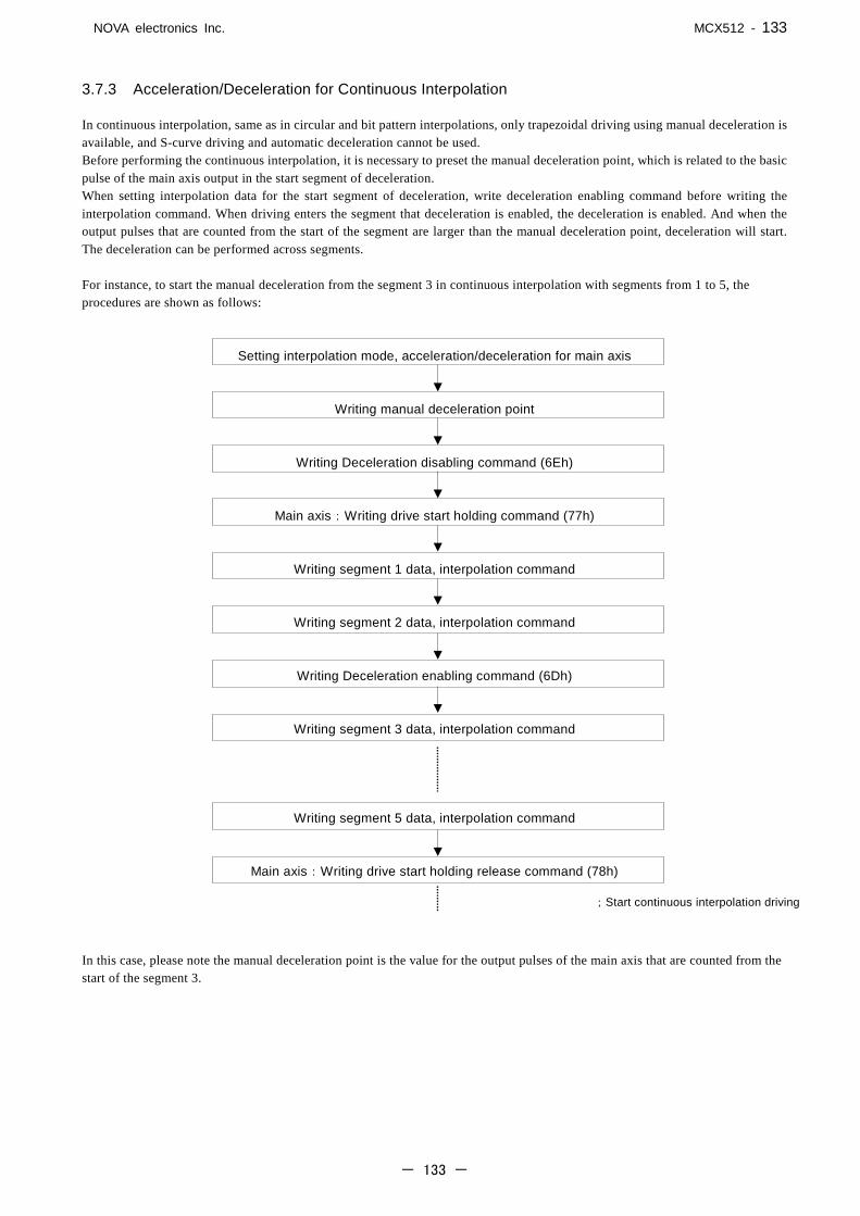
NOVA electronics Inc. MCX512 - 133
- 133 -
3.7.3 Acceleration/Deceleration for Continuous Interpolation In continuous interpolation, same as in circular and bit pattern interpolations, only trapezoidal driving using manual deceleration is available, and S-curve driving and automatic deceleration cannot be used. Before performing the continuous interpolation, it is necessary to preset the manual deceleration point, which is related to the basic pulse of the main axis output in the start segment of deceleration. When setting interpolation data for the start segment of deceleration, write deceleration enabling command before writing the interpolation command. When driving enters the segment that deceleration is enabled, the deceleration is enabled. And when the output pulses that are counted from the start of the segment are larger than the manual deceleration point, deceleration will start. The deceleration can be performed across segments. For instance, to start the manual deceleration from the segment 3 in continuous interpolation with segments from 1 to 5, the procedures are shown as follows:
Setting interpolation mode, acceleration/deceleration for main axis
Writing manual deceleration point
Writing Deceleration disabling command (6Eh)
Main axis:Writing drive start holding command (77h)
Writing segment 1 data, interpolation command
Writing segment 2 data, interpolation command
Writing Deceleration enabling command (6Dh)
Writing segment 3 data, interpolation command
Writing segment 5 data, interpolation command
Main axis:Writing drive start holding release command (78h) In this case, please note the manual deceleration point is the value for the output pulses of the main axis that are counted from the start of the segment 3.
;Start continuous interpolation driving

NOVA electronics Inc. MCX512 - 134
- 134 -
3.8 Single-step interpolation
Single-step is defined as: pulse by pulse outputting. It can be executed by a command. When using single-step, X-axis must be set to constant speed driving. The Hi level width of the output pulse from each axis is 1/2 of the pulse cycle which is decided by drive speed of X-axis. The Low level width is kept until the next command comes. Set 1 to D9 bit by interpolation mode setting command (2Ah), and it will enable the single-step interpolation mode.
3.8.1 Command Controlled Single-step Interpolation Single-step interpolation command (6Fh) is provided for single-step interpolation. The operating procedure is shown as follows.
a. Set 1 to D9 bit by interpolation mode setting command (2Ah). It will enable the single-step interpolation.
b. Set the same value to the initial and drive speeds of X axis. When the same value is set to the initial and drive speeds, driving becomes constant speed. This speed value must be faster than the writing cycle of single-step interpolation command. If the host CPU writes single step command at most 1mSEC, the user should set both speeds faster than 1000PPS.
c. Set interpolation data. (finish point, center point…)
d. Write interpolation command. Although the interpolation segment is enabled, there is no pulse output because the single-step is command controlled.
e. Write the single-step interpolation command (6Fh). The driving pulses result from the interpolation calculation will be output from each axis. Single-step interpolation command (6Fh) is written until the interpolation driving is finished.
If the user wants to stop single-step interpolation on the way, write instant stop command (57h) to X axis and wait for more than 1 pulse cycle, and then write single-step interpolation command (6Fh) again, driving will stop.
Single-step interpolation command written after the termination of interpolation driving will be disabled. 3.8.2 Attention for Single-step Interpolation
In single-step interpolation, short axis pulse equalization mode cannot be used.
D7 D6 D5 D4H L
D15 D14 D13 D12 D11 D10 D9 D8 D3 D2 D1 D0WR6 STEP
Single-step interpolation by external signal/command

NOVA electronics Inc. MCX512 - 135
- 135 -
4. I2C Serial Bus This IC has I2C serial interface bus in addition to the existing 8-bit/16-bit data bus as the interface to connect a host CPU. I2C serial bus uses only 2 lines to transfer data: serial data line (SDA) and serial clock line (SCL). Three modes of data transfer rate are available: Standard mode (100Kbit/sec), Fast mode (400Kbit/sec) and Fast mode plus (1Mbit/sec) when the load capacity of the bus is 400pF or less. Compared with 8-bit/16-bit data bus, the data transfer efficiency is decreased by approximately 10 to 100 times; but it can be performed within 1~ a few mseconds from the setting of necessary parameters (drive speed, drive pulse number, etc.) up to the start of relative driving. This is very suitable bus interface for the system that does not require high-speed setup. The following is the connection example of I2C serial bus.
Fig. 4.1-1 The Connection Example of I2C Serial Bus
4.1 Pins used in I2C Bus Mode
To use MCX512 in I2C bus mode, it is necessary to connect the following pins correctly.
Table 4.1-1 Pins in I2C Bus Mode
Signal Pin No. Description BUSMOD 32 Sets the bus mode. Setting Low level becomes in I2C bus mode. A2~A0 22~24 Address signals A2~A0 (22~24) are used as chip address setting
pins. Low level is 0, and Hi level is 1. MCX512 chips can be connected up to 8 chips at a maximum on the same bus.
SDA 25 SDA signal pin in I2C bus, which must be pulled up. SCL 26 SCL signal pin in I2C bus, which must be pulled up.
It is shared with CSN signal. When in I2C bus mode, it is used as SCL signal input.
I2CRSTN 31 Reset signal for I2C control section. Setting Low level in CLK asynchronous input will reset. Keep on Low 1μsec or more.
It is shared with H16L8 signal. 4.1.1 Pull-up Resistor (Rp) SDA and SCL signals of the bus line need pull-up resistor (Rp), and the value of pull-up resistor depends on the data transfer rate and load capacity of the bus. For more details, please refer to I2C bus specification from NXP.
SDA
SCL
I C2
Host CPU #1MCX512
#2MCX512
A0A1A2
+3.3V
GND
BUSMOD
A0A1A2
BUSMOD
Rp Rp
SCL SDA SCL SDA
+3.3V

NOVA electronics Inc. MCX512 - 136
- 136 -
4.1.2 I2CRSTN Reset At initial setting In the initial state of the system, noise may be occurred in SCL and SDA signals by switching I2C pin mode of the host CPU, and then the data transfer may not be performed correctly. In this case, please adjust the steps of I2C initial setting on the CPU side, in order to eliminate noise. If the noise is not reduced, the user needs to execute I2C Reset to MCX512 by using I2CRSTN signal after completion of I2C initial setting. Or, the user can reset the I2C control section by using RESETN signal that resets MCX512.
At data transfer When I2C communication does not work correctly such as retuning Hi from an acknowledge signal, reset the I2C control section by I2CRSTN signal. Similarly to above, the user can use RESETN signal as substitution.
4.2 I2C Bus Transmitting and Receiving
From the host CPU to MCX512, the procedures of writing to WR register and reading from RR register are as follows.
Writing Operation Reading Operation
MCX512 has only slave function.
Generate start condition
Generate stop condition
Write data
Write slave address
Generate start condition
Generate stop condition
Read data
Write slave address
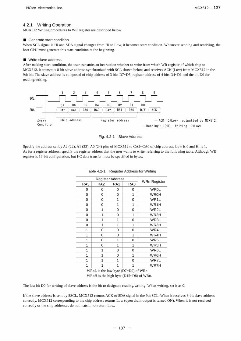
NOVA electronics Inc. MCX512 - 137
- 137 -
4.2.1 Writing Operation MCX512 Writing procedures to WR register are described below. Generate start condition When SCL signal is Hi and SDA signal changes from Hi to Low, it becomes start condition. Whenever sending and receiving, the host CPU must generate this start condition at the beginning. Write slave address After making start condition, the user transmits an instruction whether to write from which WR register of which chip to MCX512. It transmits 8-bit slave address synchronized with SCL shown below, and receives ACK (Low) from MCX512 in the 9th bit. The slave address is composed of chip address of 3 bits D7~D5, register address of 4 bits D4~D1 and the bit D0 for reading/writing.
Fig. 4.2-1 Slave Address
Specify the address set by A2 (22), A1 (23), A0 (24) pins of MCX512 to CA2~CA0 of chip address. Low is 0 and Hi is 1. As for a register address, specify the register address that the user wants to write, referring to the following table. Although WR register is 16-bit configuration, but I2C data transfer must be specified in bytes.
Table 4.2-1 Register Address for Writing
Register Address WRn Register
RA3 RA2 RA1 RA0 0 0 0 0 WR0L 0 0 0 1 WR0H 0 0 1 0 WR1L 0 0 1 1 WR1H 0 1 0 0 WR2L 0 1 0 1 WR2H 0 1 1 0 WR3L 0 1 1 1 WR3H 1 0 0 0 WR4L 1 0 0 1 WR4H 1 0 1 0 WR5L 1 0 1 1 WR5H 1 1 0 0 WR6L 1 1 0 1 WR6H 1 1 1 0 WR7L 1 1 1 1 WR7H WRnL is the low byte (D7~D0) of WRn. WRnH is the high byte (D15~D8) of WRn.
The last bit D0 for writing of slave address is the bit to designate reading/writing. When writing, set it as 0. If the slave address is sent by 8SCL, MCX512 returns ACK to SDA signal in the 9th SCL. When it receives 8-bit slave address correctly, MCX512 corresponding to the chip address returns Low (open drain output is turned ON). When it is not received correctly or the chip addresses do not match, not return Low.
SCL
SDA
1 2 3 4 5 6 7 8 9
CA2 CA1 CA0 RA3 RA2 RA1 RA0
Chip address Register address
ACK
StartCondition
R/W
D7 D0D5 D4 D1D6 D3 D2
ACK: 0(Low);outputted by MCX512
Reading:1(Hi), Writing:0(Low)

NOVA electronics Inc. MCX512 - 138
- 138 -
Write data Then, perform data writing. The data for writing is transmitted from WRn register specified by the slave address, byte by byte. From only one byte to multiple bytes continuously can be written. In the 9th SCL after sending 1 byte, if MCX512 correctly receives, it returns ACK signal of Low level on the SDA line. When the CPU receives this ACK signal, then, sends 1 byte data to be written in the next register address.
Fig. 4.2-2 Data Writing
Generate stop condition To stop data writing, the user needs to generate stop condition. When SCL signal is Hi and SDA signal changes from Low to Hi, it becomes stop condition. Whenever sending and receiving, the host CPU must generate this stop condition at the end. 4.2.2 Reading Operation MCX512 Reading procedures from RR register are described below.
Generate start condition When SCL signal is Hi and SDA signal changes from Hi to Low, it becomes start condition. Whenever sending and receiving, the host CPU must generate this start condition at the beginning. Write slave address After making start condition, the user transmits an instruction whether to read from which RR register of which chip to MCX512. It transmits 8-bit slave address synchronized with SCL shown below, and receives ACK (Low) from MCX512 in the 9th bit. The slave address is composed of chip address of 3 bits D7~D5, register address of 4 bits D4~D1 and the bit D0 for reading/writing.
Fig. 4.2-3 Slave Address
SCL
SDA
1 2 3 4 5 6 7 8 9
CA2 CA1 CA0 RA3 RA2 RA1 RA0
Chip address Register address
ACK
StartCondition
D7 D0D5 D4 D1D6 D3 D2
ACK: 0(Low);outputted by MCX512
Reading:1(Hi), Writing:0(Low)
R/W
W ACK
1 2 3 4 5 6 7 8 9 1 2 3 4 5 6 7 8 9
ACK
D7 D6 D5 D4 D3 D2 D1 D0 D7 D6 D5 D4 D3 D2 D1 D0
1 2 3 4 5 6 7 8 9
ACK
Writing data ofregister address n
Writing data ofregister address n+1
Slave addressStart Stop
SCL
SDA

NOVA electronics Inc. MCX512 - 139
- 139 -
Specify the address set by A2 (22), A1 (23), A0 (24) pins of MCX512 to CA2~CA0 of chip address. Low is 0 and Hi is 1. As for a register address, specify the register address that the user wants to read, referring to the following table. Although RR register is 16-bit configuration, but I2C data transfer must be specified in bytes.
Table 4.2-2 Register Address for Reading
Register Address RRn Register
RA3 RA2 RA1 RA0 0 0 0 0 RR0L 0 0 0 1 RR0H 0 0 1 0 RR1L 0 0 1 1 RR1H 0 1 0 0 RR2L 0 1 0 1 RR2H 0 1 1 0 RR3L 0 1 1 1 RR3H 1 0 0 0 RR4L 1 0 0 1 RR4H 1 0 1 0 RR5L 1 0 1 1 RR5H 1 1 0 0 RR6L 1 1 0 1 RR6H 1 1 1 0 RR7L 1 1 1 1 RR7H
RRnL is the low byte (D7~D0) of RRn. RRnH is the high byte (D15~D8) of RRn.
The last bit D0 for writing of slave address is the bit to designate reading/writing. When reading, set it to 1. If the slave address is sent by 8SCL, MCX512 returns ACK to SDA signal in the 9th SCL. When it receives 8-bit slave address correctly, MCX512 corresponding to the chip address returns Low (open drain output is turned ON). When it is not received correctly or the chip addresses do not match, not return Low. Read data Then, perform data reading. The data for reading is outputted from RRn register specified by the slave address on the SDA line, byte by byte. From only one byte to multiple bytes continuously can be read. In the 9th SCL after receiving 1 byte, if the CPU correctly receives, it is necessary to return ACK signal of Low level on the SDA line. However, in the last data that comes stop condition next, return ACK signal of Hi level.
Fig. 4.2-4 Data Reading
Generate stop condition To stop data reading, the user needs to generate stop condition. When SCL signal is Hi and SDA signal changes from Low to Hi, it becomes stop condition. Whenever sending and receiving, the host CPU must generate this stop condition at the end.
R ACK
1 2 3 4 5 6 7 8 9 1 2 3 4 5 6 7 8 9
ACK
D7 D6 D5 D4 D3 D2 D1 D0 D7 D6 D5 D4 D3 D2 D1 D0
1 2 3 4 5 6 7 8 9
ACK
Reading data ofregister address n
Reading data ofregister address n+1
Slave addressStart Stop
SCL
SDA

NOVA electronics Inc. MCX512 - 140
- 140 -
4.2.3 Notes on Using I2C Serial Bus
• When writing to WR0 register, the high byte (H) must be written first, followed by the low byte (L). The user cannot write 2 bytes continuously. It is necessary to set and write each slave address individually. If the low byte is written, the command is executed immediately to the axis prior specified.
• When reading data, as for ACK signal at reading of the last data, the CPU must return Hi level of ACK signal on the SDA line. If returns Low level, this IC cannot terminate communication correctly.
• When using interrupt related to INT0N signal, the user cannot read RR0H. If reads RR0H, the interrupt related to INT0N signal may be cleared. If the user needs to read RR0H when using interrupt, please contact us.
• When reading RR1 register, be sure to read 2 bytes (RR1L, RR1H) from RR1L. If reads only 1 byte of RR1L, the interrupt of RR1H may be cleared.
• Repeat start condition is not available. 4.2.4 Connection Example The connection example of this IC with CPU is as follows.
① Fix BUSMOD to GND, and set I2C bus mode. ② Determine chip address by A2, A1, A0 signals. ③ Fix parallel bus signal (floating input) to GND or VCC. ④ Connect I2CRSTN as necessary, which is not needed unless noise is occurred on the SCL, SDA line from the CPU side at initial setting.
⑤ Pull-up resistors are essential on the SCL, SDA lines.
Host CPU MCX512
A0
A1
A2
BUSMOD
SCL
SDA
Example of Chip address:1,0,0
SCL
SDA
D15-D8
WRN
RDN
A3
Port Output I2CRSTN
+3.3V
3.3K 3.3K
D7-D0
27
28
1-8
11-18
21
26
25
31
22
23
24
32
+3.3V +3.3V
1
2
3
4
5

NOVA electronics Inc. MCX512 - 141
- 141 -
4.2.5 Control Example The following three examples show the flow of controlling the IC using I2C serial bus. The user can download sample programs for controlling each type of CPU including these three examples, from our web site: http://www.novaelec.co.jp/ (1) Write command (2) Write data (3) Read data (1) Write command To write a command, the user needs to write an execution axis and command to WR0 register. At this time, if the low byte of WR0L is written, a command will be executed immediately. So the user needs to specify the axis before issuing a command. As shown below, specify an axis at ①, and then write a command at ②. ① Write an axis assignment to WR0H. ② Write a command to WR0L
Generate start condition
Generate stop condition
Write axis assignment (WR0H)
Write slave address
Generate start condition
Generate stop condition
Write command (WR0L)
Write slave address

NOVA electronics Inc. MCX512 - 142
- 142 -
(2) Write data To perform data writing such as parameter settings, write parameters to WR6, WR7 registers and then write an axis assignment and command to WR0 register. Regarding writing of WR0 register, as described in (1) Write command, a command must be written after the axis assignment. ① Write data to WR6, 7 ② Write axis assignment to WR0H ③ Write data writing command to WR0L
Generate start condition
Generate stop condition
Write data (WR6, WR7)
Write slave address
Generate start condition
Generate stop condition
Write axis assignment (WR0H)
Write slave address
Generate start condition
Generate stop condition
Write data writing command (WR0L)
Write slave address

NOVA electronics Inc. MCX512 - 143
- 143 -
(3) Read data To perform data reading, write an axis assignment and command to WR0 register, and then read RR6, RR7 registers. Regarding writing of WR0 register, as described in (1) Write command, a command must be written after the axis assignment.
① Write axis assignment to WR0H ② Write data reading command to WR0L ③ Read from RR6, 7
Generate start condition
Generate stop condition
Write axis assignment (WR0H)
Write slave address
Generate start condition
Generate stop condition
Write data reading command (WR0L)
Write slave address
Generate start condition
Generate stop condition
Read data (RR6, 7)
Write slave address
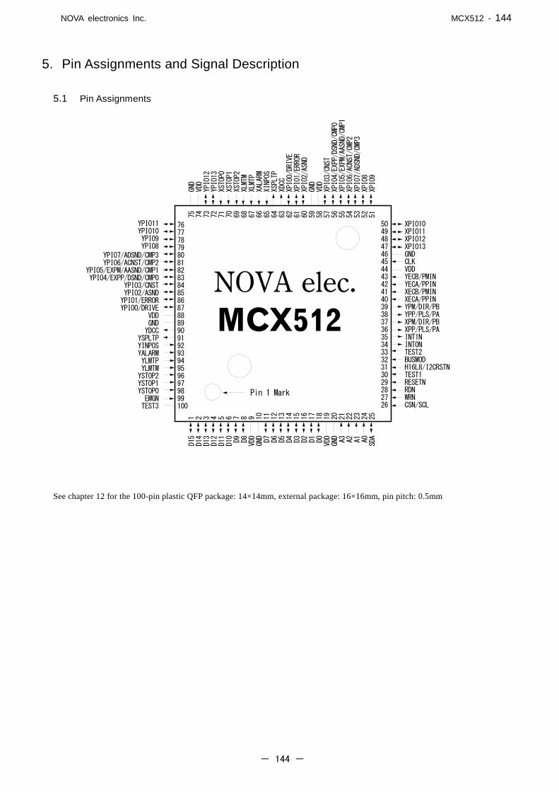
NOVA electronics Inc. MCX512 - 144
- 144 -
5. Pin Assignments and Signal Description
5.1 Pin Assignments
See chapter 12 for the 100-pin plastic QFP package: 14×14mm, external package: 16×16mm, pin pitch: 0.5mm
Pin 1 Mark
D15
D14
D13
D12
D11
D10 D9 D8 VDD
GND D7 D6 D5 D4 D3 D2 D1 D0 VDD
GND A3 A2 A1 A0 SDA
1 2 3 4 5 6 7 8 9 10 11 12 13 14 15 16 17 18 19 20 21 22 23 24 25
75 74 73 72 71 70 69 68 67 66 65 64 63 62 61 60 59 58 57 56 55 54 53 52 51
GND
VDD
YPIO12
YPIO13
XSTOP0
XSTOP1
XSTOP2
XLMTM
XLMTP
XALARM
XINPOS
XSPLTP
XDCC
XPIO0/DRIVE
XPIO1/ERROR
XPIO2/ASND
GND
VDD
XPIO3/CNST
XPIO4/EXPP/DSND/CMP0
XPIO5/EXPM/AASND/CMP1
XPIO6/ACNST/CMP2
XPIO7/ADSND/CMP3
XPIO8
XPIO9
50494847464544434241403938373635343332313029282726
767778798081828384858687888990919293949596979899100
YPIO11YPIO10YPIO9YPIO8
YPIO7/ADSND/CMP3YPIO6/ACNST/CMP2
YPIO5/EXPM/AASND/CMP1YPIO4/EXPP/DSND/CMP0
YPIO3/CNSTYPIO2/ASNDYPIO1/ERRORYPIO0/DRIVE
VDDGNDYDCC
YSPLTPYINPOSYALARMYLMTPYLMTMYSTOP2YSTOP1YSTOP0EMGNTEST3
NOVA elec.MCX512
XPIO10XPIO11XPIO12XPIO13GNDCLKVDDYECB/PMINYECA/PPINXECB/PMINXECA/PPINYPM/DIR/PBYPP/PLS/PAXPM/DIR/PBXPP/PLS/PAINT1NINT0NTEST2BUSMODH16L8/I2CRSTNTEST1RESETNRDNWRNCSN/SCL

NOVA electronics Inc. MCX512 - 145
- 145 -
5.2 Signal Description
See chapter 5.3 for description of input/output logic. The input signals with – F – symbol indicates that an integral filter circuit is available in the internal input column of this IC.
Signal Name Pin No. Input/Output Signal Description
CLK 45 Input A
Clock: clock signal for internal synchronous loop of MCX512 The standard frequency is 16 MHz. This signal is for drive speed, acceleration/deceleration and acceleration/deceleration increasing rate. If the frequency setting is not 16 MHz, the setting values of speed and acceleration/deceleration are different.
D15~D0 1~8,
11~18 Bi-directional
A
Data Bus (D15~D0): 3-state bi-direction 16-bit data bus When CSN=Low and RDN=Low, these signals are for outputting. Otherwise, they are high impedance inputs. If 8-bit data bus is used and D15~D8 are not used, they should be connected to VDD or GND through high impedance (about 10K~100 kΩ). In I2C mode, can be used as general purpose input signals.
A3~A0 21~24 Input A Address: address signal for the host CPU to access the write/read registers If 16-bit data bus is used, A3 cannot be used and should be connected to GND. In I2C mode, A2~A0 are used as chip address setting pins.
SDA 25 Bi-directional
C
I2CSDA: SDA signal in I2C mode.
CSN/SCL 26 Input A Chip Select/I2C SCL: input signal for selecting I/O device for MCX512
Set to the Low level for data reading and writing. In I2C mode, used as SCL signal.
WRN 27 Input A
Write Strobe: its level is Low while data is being written to MCX512. While WRN is Low, CSN and A3~A0 must be determined. Around when WRN is up (↑), the levels of D15~D0 must be determined because the data is latched in the write register when WRN is up (↑).
RDN 28 Input A Read Strobe: its level is Low while data is being read from MCX512. Set CSN to Low and RDN to Low, and while RDN is Low, the read register data selected by A3~A0 address signals is output to the data bus.
RESETN 29 Input A
Reset: reset (return to the initial setting) signal for MCX512. Setting RESETN to Low for more than 8 CLK cycles resets MCX512. This IC must be reset by RESETN signal when the power is on. [Note] If there is no clock input to MCX512, setting RESETN to Low cannot reset this IC
H16L8 /I2CRSTN
31 Input B
Hi=16bit, Low=8bit: data bus width selection for 16-bit/8-bit When set to Hi, 16-bit data bus is selected for processing the 16-bit data reading/writing in IC; when set to Low, 8-bit data bus (D7~D0) is active for data reading/writing. In I2C mode, used as I2C Reset. Setting Low resets the I2C control section inside of the IC.
BUSMOD 32 Input B Bus Mode: Selects CPU bus mode. When set to Hi, it is in 16bit/8bit parallel bus mode, and when set to Low, it is in I2C serial bus mode.
INT0N 34 Output B Interrupt: outputs an interrupt signal to the host CPU. If any interrupt factor except interpolation pre-buffer generates an interrupt, INT0N becomes Low level. When an interrupt is released, it will return to the Hi-Z level.
INT1N 35 Output B Interrupt: outputs an interrupt signal to the host CPU. If interrupt factor by interpolation pre-buffer generates an interrupt, INT1N becomes Low level. When an interrupt is released, it will return to the Hi-Z level.
XPP/PLS/PA YPP/PLS/PA
36 38
Output A
Pulse +/Pulse/Pulse Phase A: +direction dive pulse outputting It is Low level at reset, and when driving is started, DUTY 50% (at constant speed) of the plus drive pulses is output. When the 1-pulse 1-direction mode is selected, this terminal is for drive output. When the quadrature pulse mode is selected, this terminal is for A-phase signal output.
NOVA electronics Inc. MCX512 - 146
- 146 -
Signal Name Pin No. Input/Output Signal Description
XPM/DIR/PB YPM/DIR/PB
37 39
Output A
Pulse -/Direction/Pulse Phase B: -direction dive pulse outputting It is Low level at reset, and when driving is started, DUTY 50% (at constant speed) of the plus drive pulses is output. When the 1-pulse 1-direction mode is selected, this terminal is the direction signal. When the quadrature pulse mode is selected, this terminal is for B-phase signal output.
XECA/PPIN YECA/PPIN
40 42
Input B -F-
Encoder-A/Pulse+in: signal for encoder phase-A input This input signal, together with phase-B signal, will make the Up/Down pulse transformation to be the input count of real position counter. When the Up/Down pulse input mode is selected, this terminal is for UP pulses input. When the input pulse is up (↑), the real position counter is counted up.
XECB/PMIN YECB/PMIN
41 43
Input B -F-
Encoder-B/Pulse-in: signal for encoder phase-B input This input signal, together with phase-A signal, will make the Up/Down pulse transformation to be the input count of real position counter. When the Up/Down pulse input mode is selected, this terminal is for DOWN pulses input. When the input pulse is up (↑), the real position counter is counted down.
XSTOP2~0 YSTOP2~0
69,70,71 96,97,98
Input B -F-
Stop2~0: input signal to perform decelerating/instant stop These signals can be used for HOME searching. When the filter function is disabled, the active pulse width must be 2CLK or more. Enable/disable and logical levels can be set for STOP2~STOP0. In automatic home search, STOP0 can be assigned to a near home search signal, STOP1 to a home signal and STOP2 to an encoder Z-phase signal. The signal status can be read from RR3 register Page0.
XLMTP YLMTP
67 94
Input B -F-
Over Run Limit +: signal of +direction over limit During the +direction drive pulse outputting, decelerating stop or instant stop will be performed once this signal is active. When the filter function is disabled, the active pulse width must be 2CLK or more. Enable/disable, decelerating stop/instant stop and logical levels can be set as commands. When the limit signal is enabled and this signal is in its active level during +direction driving, HLMT+ bit of RR2 register becomes 1. The signal status can be read from RR3 register Page0, and this signal can be used to search a home position.
XLMTM YLMTM
68 95
Input B -F-
Over Run Limit -: signal of -direction over limit During the -direction drive pulse outputting, decelerating stop or instant stop will be performed once this signal is active. When the filter function is disabled, the active pulse width must be 2CLK or more. Enable/disable, decelerating stop/instant stop and logical levels can be set as commands. When the limit signal is enabled and this signal is in its active level during -direction driving, HLMT- bit of RR2 register becomes 1. The signal status can be read from RR3 register Page0, and this signal can be used to search the home position.
XINPOS YINPOS
65 92
Input B -F-
Inposition: input signal for servo driver in-position Enable/disable and logical level can be set as commands. When enabled and after driving is finished, DRIVE bit of main status register returns to 0 after this signal becomes active. The signal status can be read from RR3 register Page0.
XALARM YALARM
66 93
Input B -F-
Servo Alarm: input signal for servo driver alarm Enable/disable and logical level can be set as commands. When enabled and when changes to active level during the driving, ALARM bit of RR2 register becomes 1 and driving stops instantly. The signal status can be read from RR3 register Page0.

NOVA electronics Inc. MCX512 - 147
- 147 -
Signal Name Pin No. Input/Output Signal Description
XPIO13 YPIO13
47 72
Bi-directional B
-F-
Universal Input Output13: general purpose input/output signals (PIO13). The status of general input signal (PIO13), XPIO13 can be read from RR4 register, YPIO13 can be read from RR5 register. General purpose output signal (PIO13) can set Hi/Low by writing the 1/0 data, XPIO13 to WR4 register and YPIO13 to WR5 register.
XPIO12 YPIO12
48 73
Bi-directional B
-F-
Universal Input Output12: general purpose input/output signals (PIO12). For the status of general input signal (PIO12) is same as PIO13. For general output signal (PIO12), same as PIO13.
XPIO11 YPIO11
49 76
Bi-directional B
-F-
Universal Input Output11: general purpose input/output signals (PIO11). For the status of general input signal (PIO11) is same as PIO13. For general output signal (PIO11), same as PIO13.
XPIO10 YPIO10
50 77
Bi-directional B
-F-
Universal Input Output10: general purpose input/output signals (PIO10). For the status of general input signal (PIO10) is same as PIO13. For general output signal (PIO10), same as PIO13.
XPIO9 YPIO9
51 78
Bi-directional B
-F-
Universal Input Output9: general purpose input/output signals (PIO9). For the status of general input signal (PIO9) is same as PIO13. For general output signal (PIO9), same as PIO13.
XPIO8 YPIO8
52 79
Bi-directional B
-F-
Universal Input Output8: general purpose input/output signals (PIO8). For the status of general input signal (PIO8) is same as PIO13. For general output signal (PIO8), same as PIO13.
XPIO7/ADSND/CMP3 YPIO7/ADSND/CMP3
53 80
Bi-directional B
-F-
Universal Input Output7/Acceleration Descend/Compare MR3: general purpose input/output signals (PIO7), acceleration decreasing status output signal (ADSND), MR3 comparison output (CMP3) share the same pin. The signal mode to use can be selected. General purpose input signal (PIO7) status can be read, XPIO7 from RR4 register and YPIO7 from RR5 register. General purpose output signal (PIO7) can set Hi/Low by writing the 1/0 data, XPIO7 to WR4 register and YPIO7 to WR5 register. For synchronous action, it can be used as the input signal of an activation factor. Acceleration decreasing status output (ADSND) becomes Hi while the driving command is executed and when acceleration decrease. MR3 comparison output (CMP3) becomes Hi when it satisfies the comparison condition of multi-purpose register MR3.
XPIO6/ACNST/CMP2 YPIO6/ACNST/CMP2
54 81
Bi-directional B
-F-
Universal Input Output6/Acceleration Constant/Compare MR2: general purpose input/output signals (PIO6), acceleration constant status output signal (ACNST), MR2 comparison output (CMP2) share the same pin. The signal mode to use can be selected. About general purpose input/output signals (PIO6), it is the same as PIO7. For synchronous action, it can be used as the input signal of an activation factor. Acceleration constant status output (ACNST) becomes Hi while the driving command is executed and when acceleration keeps constant. MR2 comparison output (CMP2) becomes Hi when it satisfies the comparison condition of multi-purpose register MR2.

NOVA electronics Inc. MCX512 - 148
- 148 -
Signal Name Pin No. Input/Output Signal Description
XPIO5/EXPM/AASND/CMP1
YPIO5/EXPM/AASND/CMP1
55 82
Bi-directional B
-F-
Universal Input Output5/External Operation-/Acceleration Ascend/ Compare MR1: general purpose input/output signals (PIO5), External Operation- (EXPM), acceleration increasing status output signal (AASND), MR1 comparison output (CMP1) share the same pin. The signal mode to use can be selected. About general purpose input/output signals (PIO5), it is the same as PIO7. For synchronous action, it can be used as the input signal of an activation factor. External Operation- (EXPM) is -direction drive starting signal from external source. When the relative position driving is commanded from an external source, -direction relative position driving starts by down (↓) of this signal. When the continuous pulse driving is commanded from an external source, -direction continuous pulse driving is performed while this signal is on the Low level. In the manual pulsar mode, the encoder B-phase signal is input to this pin. Acceleration increasing status output (AASND) becomes Hi while the driving command is executed and when acceleration increase. MR1 comparison output (CMP1) becomes Hi when it satisfies the comparison condition of multi-purpose register MR1.
XPIO4/EXPP/DSND/CMP0
YPIO4/EXPP/DSND/CMP0
56 83
Bi-directional B
-F-
Universal Input Output4/External Operation+/Descend/Compare MR0: general purpose input/output signals (PIO4), External Operation+ (EXPP), deceleration status output signal (DSND), MR0 comparison output (CMP0) share the same pin. The signal mode to use can be selected. About general purpose input/output signals (PIO4), it is the same as PIO7. For synchronous action, it can be used as the input signal of an activation factor. External Operation+ (EXPP) is +direction drive starting signal from external source. When the relative position driving is commanded from an external source, +direction relative position driving starts by down (↓) of this signal. When the continuous pulse driving is commanded from an external source, +direction continuous pulse driving is performed while this signal is on the Low level. In the manual pulsar mode, the encoder A-phase signal is input to this pin. Deceleration status output (DSND) becomes Hi while the driving command is executed and when in deceleration. MR0 comparison output (CMP0) becomes Hi when it satisfies the comparison condition of multi-purpose register MR0.
XPIO3/CNST YPIO3/CNST
57 84
Bi-directional B
-F-
Universal Input Output3/Constant: general purpose input/output signals (PIO3), constant speed driving status output signal (CNST) share the same pin. The signal mode to use can be selected. About general purpose input/output signals (PIO3), it is the same as PIO7. For synchronous action, it can be used as the input signal of an activation factor or the output signal of synchronous pulses of the action. The logical level of synchronous pulses and pulse width can be set as commands. Constant speed driving status output (CNST) becomes Hi while the driving command is executed and when in constant speed driving.

NOVA electronics Inc. MCX512 - 149
- 149 -
Signal Name Pin No. Input/Output Signal Description
XPIO2/ASND YPIO2/ASND
60 85
Bi-directional B
-F-
Universal Input Output2/Ascend: general purpose input/output signals (PIO2), acceleration status output signal (ASND) share the same pin. The signal mode to use can be selected. About general purpose input/output signals (PIO2), it is the same as PIO7. For synchronous action, it is the same as PIO3. Acceleration status output (ASND) becomes Hi while the driving command is executed and when in acceleration.
XPIO1/ERROR YPIO1/ERROR
61 86
Bi-directional B
-F-
Universal Input Output1/Error: general purpose input/output signals (PIO1), error status output signal (ERROR) share the same pin. The signal mode to use can be selected. About general purpose input/output signals (PIO1), it is the same as PIO7. For synchronous action, it is the same as PIO3. Error status output (ERROR) becomes Hi while an error occurs.
XPIO0/DRIVE YPIO0/DRIVE
62 87
Bi-directional B
-F-
Universal Input Output0/Drive: general purpose input/output signals (PIO0), drive status output signal (DRIVE) share the same pin. The signal mode to use can be selected. About general purpose input/output signals (PIO1), it is the same as PIO7. For synchronous action, it is the same as PIO3. Drive status display output (DRIVE) is set to High level while drive pulses are output. At execution of automatic home search, this signal is set to High level. The DRIVE signal is set to High level until INPOS becomes active when INPOS signal for the serve motor is enabled by mode selection.
XDCC YDCC
63 90
Output A
Deviation Counter Clear: deviation counter clear output signal A deviation counter clear output (DCC) signal is output for a server motor driver. The signal can be output by mode setting in automatic home search. It can also be output by a command.
XSPLTP YSPLTP
64 91
Output A
Split Pulse: Outputs split pulses Split pulse output can be started and stopped by a synchronous action or a command. Split length, pulse width and pulse number can be set by a command. And output logic, with or without starting pulse can be set as commands.
EMGN 99 Input B -F-
Emergency Stop: input signal to perform the emergency stop for all axes. When this signal is set to Low level during the driving, driving of all axes including interpolation driving stops immediately and EMG bit of RR2 register becomes 1. When the filter function is disabled, the low level pulse width must be more than 2CLK. [Note] For this signal, its logical level cannot be selected.
TEST1 30 - Test: input terminal for internal-circuit test Make sure to be open or connected to GND. This is pulled up to GND with 50kΩ inside the IC.
TEST2 33 - Test: input terminal for internal-circuit test Make sure to be open or connected to GND. This is pulled down to GND with 50kΩ inside the IC.
TEST3 100 - Test: input terminal for internal-circuit test Make sure to be open or connected to GND. This is pulled down to GND with 50kΩ inside the IC.
GND 10,20,46, 59,75,89
- Ground (0V) Terminal All of the pins must be connected to 0V.
VDD 9,19,44,
58,74,88,
+3.3V Power Terminal All of the pins must be connected to each power without fail.

NOVA electronics Inc. MCX512 - 150
- 150 -
5.3 Input/Output Logic
Input A LVTTL Schmitt trigger input, which is high impedance because there is no pull high resister for those signals in this
IC. Input is 5V tolerant. 3.3V and 5V type output (CMOS level and TTL level) can be connected. The user should connect to GND or VDD if the input is not used.
Input B LVTTL Schmitt trigger input, which is pulled up with 50kΩ in the IC. Input is 5V tolerant. 3.3V and 5V type output (CMOS level and TTL level) can be connected. The user should be Open or connect to VDD if the input is not used. The signal with – F – symbol has an integral filter circuit in the internal input column of this IC.
Output A It is 3.3V type CMOS level output, 6mA driving buffer (Hi level output current IOH=−6mA, VOH=2.6Vmin, Low level output current IOL=6mA, VOL=0.4Vmax). When in Hi level output, do not apply voltage more than the output voltage from outside. 5V type input can be connected when the other input is TTL level. If the other input is 5V type CMOS level, it cannot be connected. ※Note1
Output B It is open collector type output, 12mA driving buffer, (Low level output current IOL=12mA, VOL=0.4Vmax). Pull up to +3.3V with high impedance if this output is used. It can also be connected to TTL level 5V type IC.
Bi-directional
A
Input side is 5V tolerant LVTTL Schmitt trigger. Because there is no pull high resister for those signals in this IC, the user should pull up the data bus with high impedance. The user should pull up to +3.3V with high impedance (about 10k~100kΩ) when bits D15~D8, PIN6, 5 are not used. It is better to be through high impedance rather than to pull-up/pull-down directly because this signal is bi-directional. When in Hi level output, do not apply voltage more than the output voltage from outside. Output side is 3.3V type CMOS level output, 12mA driving buffer (Hi level output current IOH=−12mA, VOH=2.6Vmin, Low level output current IOL=12mA, VOL=0.4Vmax). 5V type bi-directional IC can be connected when the other input is TTL level. If the other input is 5V type CMOS level, it cannot be connected. ※Note1
Bi-directional
B
Input side is 5V tolerant LVTTL Schmitt trigger, which is pulled up with 50kΩ (Typ.) in the IC. When in Hi level output, do not apply voltage more than the output voltage from outside. Output side is 3.3V type CMOS level output, 6mA driving buffer (Hi level output current IOH=−6mA, VOH=2.6Vmin, Low level output current IOL=6mA, VOL=0.4Vmax). 5V type bi-directional IC can be connected when the other input is TTL level. If the other input is 5V type CMOS level, it cannot be connected. ※Note1 The signal with – F – symbol has an integral filter circuit in the internal input column of this IC.
Bi-directional
C
I2C exclusive SDA signal. Input side is 5V tolerant LVTTL Schmitt trigger. Because there is no pull high resister for those signals in this IC, the user should pull up the data bus with high impedance. Output side is open collector type output of 6mA driving buffer. When used as SDA signal, pull up to VDD through a resistor. The user should pull up to VDD with high impedance or connect to GND directly if this is not used.
Note1: Even if the output signals of output A and Bi-directional A, B are pulled up to 5V through resister, Hi level output voltage cannot raise to Hi level input voltage of 5V type CMOS. Please don’t design the logic like this.
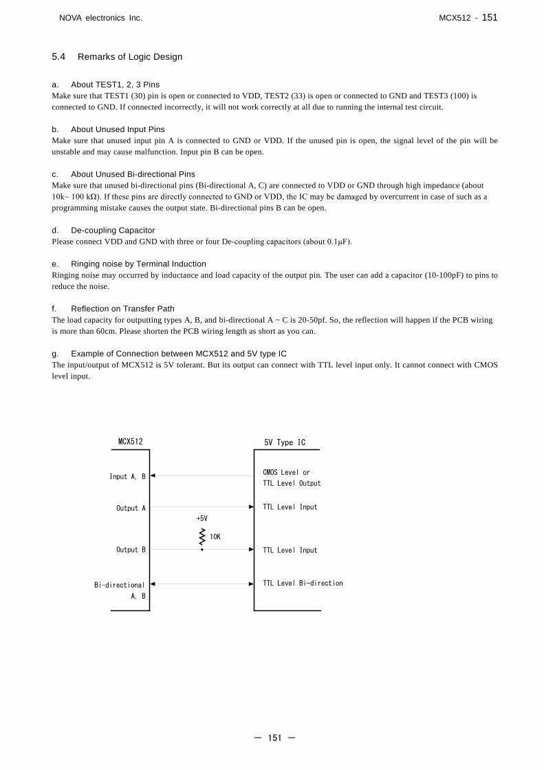
NOVA electronics Inc. MCX512 - 151
- 151 -
5.4 Remarks of Logic Design
a. About TEST1, 2, 3 Pins Make sure that TEST1 (30) pin is open or connected to VDD, TEST2 (33) is open or connected to GND and TEST3 (100) is connected to GND. If connected incorrectly, it will not work correctly at all due to running the internal test circuit. b. About Unused Input Pins Make sure that unused input pin A is connected to GND or VDD. If the unused pin is open, the signal level of the pin will be unstable and may cause malfunction. Input pin B can be open. c. About Unused Bi-directional Pins Make sure that unused bi-directional pins (Bi-directional A, C) are connected to VDD or GND through high impedance (about 10k~ 100 kΩ). If these pins are directly connected to GND or VDD, the IC may be damaged by overcurrent in case of such as a programming mistake causes the output state. Bi-directional pins B can be open.
d. De-coupling Capacitor Please connect VDD and GND with three or four De-coupling capacitors (about 0.1μF). e. Ringing noise by Terminal Induction Ringing noise may occurred by inductance and load capacity of the output pin. The user can add a capacitor (10-100pF) to pins to reduce the noise. f. Reflection on Transfer Path The load capacity for outputting types A, B, and bi-directional A ~ C is 20-50pf. So, the reflection will happen if the PCB wiring is more than 60cm. Please shorten the PCB wiring length as short as you can.
g. Example of Connection between MCX512 and 5V type IC The input/output of MCX512 is 5V tolerant. But its output can connect with TTL level input only. It cannot connect with CMOS level input.
10K
+5V
Input A, B
Output A
Output B
Bi-directional
A, B
TTL Level Bi-direction
TTL Level Input
TTL Level Input
CMOS Level or
TTL Level Output
MCX512 5V Type IC

NOVA electronics Inc. MCX512 - 152
- 152 -
6. Register This chapter describes the user how to access all the registers in MCX512, and what are the mapping addresses of these registers.
6.1 Register Address by 16-bit Data Bus
As shown in the table below, when 16-bit data bus is used, the access address of read/write register is 8-bit.
Write Register in 16-bit Data Bus
All registers are 16-bit length. Address
A2 A1 A0 Symbol Register Name Descriptions
0 0 0 WR0 Command Register ・for axis assignment and setting command
0 0 1 XWR1 YWR1
X-axis Mode register 1 Y-axis Mode register 1
・for setting the valid/invalid of interrupt
0 1 0 XWR2 YWR2
X-axis Mode register 2 Y-axis Mode register 2
・for setting the logical levels and enable/disable of external decelerating stop ・for setting the logical levels and enable/disable of servo motor signal ・for setting the limit signal mode and software limit mode
0 1 1 XWR3 YWR3
X-axis Mode register 3 Y-axis Mode register 3
・for setting the auto and manual deceleration ・for setting the acceleration/deceleration mode (symmetry/ non-symmetry, linear acceleration/deceleration, S-curve acceleration/deceleration) ・for setting the drive pulse output mode and pins ・for setting the encoder input signal mode and pins
1 0 0 WR4
Output register 1 ・for setting the output values of X-axis general purpose input/output signals XPIO13~0
1 0 1 WR5
Output register 2 ・for setting the output values of Y-axis general purpose input/output signals YPIO13~0
1 1 0 WR6 Data writing register 1 ・for setting the low word 16-bit (D15~D0) for data writing 1 1 1 WR7 Data writing register 2 ・for setting the high word 16-bit (D31~D16) for data writing
As shown in the table above, each axis has WR1, WR2 and WR3 mode registers, which will be written by the same address. The host CPU specifies which axis should be accessed depends on the axis of written command just before. Or the user can specify the axis by writing NOP command with axis assignment.
The bits of WR1, WR2, WR3, WR4 and WR5 are cleared to 0 at reset.

NOVA electronics Inc. MCX512 - 153
- 153 -
Read Register in 16-bit Data Bus
All registers are 16-bit length. Address
A2 A1 A0 Symbol Register Name Contents
0 0 0 RR0 Main status register ・driving status and error status
・ready for interpolation, quadrant for circle interpolation and
continuous interpolation pre-buffer stack counter (SC)
0 0 1 XRR1 YRR1
X-axis Status register 1 Y-axis Status register 1
・interrupt message
0 1 0 XRR2 YRR2
X-axis Status register 2 Y-axis Status register 2
・error message ・finishing status
0 1 1 XRR3 YRR3
X-axis Status register 3 Y-axis Status register 3
Page 0 ・input signal status ・automatic home search execution state Page 1 ・enable/disable of synchronous action set ・acceleration/deceleration status, increase/decrease status of
acceleration/deceleration ・status of timer and split pulse operation
1 0 0 RR4 PIO read register 1 ・X-axis general purpose input/output signal status 1 0 1 RR5 PIO read register 2 ・Y-axis general purpose input/output signal status 1 1 0 RR6 Data reading register 1 ・low word of data register (D15~D0) 1 1 1 RR7 Data reading register 2 ・high word of data register (D31~D16)
As with Write Register, each axis has RR1, RR2 and RR3 status registers, which will be read by the same address. The host
CPU specifies which axis should be accessed depends on the axis of written command just before. Or the user can specify the axis by writing NOP command with axis assignment.
Regarding RR3 register, there are 2 kinds: Page 0 and Page1. The page can be specified by writing RR3 page display command (7Ah, 7Bh). It will be Page 0 at reset.
NOVA electronics Inc. MCX512 - 154
- 154 -
6.2 Register Address by 8-bit Data Bus
For the 8-bit data bus access, the 16-bit data bus can be divided into high and low word byte. As shown in the table below, xxxxL is the low word byte (D7~D0) of 16-bit register xxxx, xxxxH is the high word byte (D15~8) of 16-bit register xxxx. To the command register (WR0L, WR0H), make sure to first write the high word byte (WR0H), and next write the low word byte (WR0L).
Write Register in 8-bit Data Bus
Address A3 A2 A1 A0
Write Register
0 0 0 0 WR0L 0 0 0 1 WR0H 0 0 1 0 WR1L 0 0 1 1 WR1H 0 1 0 0 WR2L 0 1 0 1 WR2H 0 1 1 0 WR3L 0 1 1 1 WR3H 1 0 0 0 WR4L 1 0 0 1 WR4H 1 0 1 0 WR5L 1 0 1 1 WR5H 1 1 0 0 WR6L 1 1 0 1 WR6H 1 1 1 0 WR7L 1 1 1 1 WR7H
Read Register in 8-bit Data Bus
Address A3 A2 A1 A0
Read Register
0 0 0 0 RR0L 0 0 0 1 RR0H 0 0 1 0 RR1L 0 0 1 1 RR1H 0 1 0 0 RR2L 0 1 0 1 RR2H 0 1 1 0 RR3L 0 1 1 1 RR3H 1 0 0 0 RR4L 1 0 0 1 RR4H 1 0 1 0 RR5L 1 0 1 1 RR5H 1 1 0 0 RR6L 1 1 0 1 RR6H 1 1 1 0 RR7L 1 1 1 1 RR7H
6.3 Register Address by I2C Serial Interface Bus Mode
When MCX512 is used in I2C serial interface bus, the user can access a register address by slave address control. Follow the same way to specify a register address as described in chapter 6.2, dividing the 16 bit data bus into high and low word byte. For more details of I2C serial interface bus, see chapter 4.

NOVA electronics Inc. MCX512 - 155
- 155 -
6.4 Command Register: WR0
Command register is used for axis assignment and command registration for each axis in MCX512. The register is composed of the bit for axis assignment and setting command code. After command code has been written to this register, the command will be executed immediately. The data writing command such as a drive speed setting must be written into registers WR6 and WR7 first. Otherwise, when the reading command is engaged, the data will be written and set, through IC internal circuit, to registers RR6 and RR7. When using the 8-bit data bus, the user must write the high word byte (H) first, and the low word byte (L) next. A command will be executed to the axis to be prior assigned immediately after writing the low word byte. It requires 125nsec (maximum) to access the command code when CLK=16MHz. Please don’t write the next command during the period of time.
D7~0 Command code setting. D9~8 Axis assignment. When the bits of the axis are set as 1, the axis is assigned. The assignment is not limited only for one axis,
but for multi-axes simultaneously. It is possible to write the same parameters also. However, for data reading, assign only one axis.
Other bits must be set as 0; otherwise, the unknown situation could happen due to IC internal circuit test.
6.5 Mode Register1: WR1
Each X and Y axis has mode register WR1 individually. The host CPU specifies the mode register of which axis should be accessed depends on the axis of written command just before. Or the user can specify the axis by writing NOP command with axis assignment. Mode register WR1 is used for setting each interrupt factor to enable/disable. Each bit is set: 1: enable, 0: disable
D3~0 CMR3~0 Interrupt occurs when the comparison result of multi-purpose register MR3~0 with a comparative object
changes to meet the comparison condition. Use multi-purpose register mode setting command (20h) to set the object which the user wants to compare with MR3~0 and comparison condition.
D4 D-STA Interrupt occurs at the start of driving. D5 C-STA Interrupt occurs when pulse output starts at constant speed area in acceleration/deceleration driving. D6 C-END Interrupt occurs when pulse output is finished at constant speed area in acceleration/deceleration driving. D7 D-END Interrupt occurs when the driving is finished. D8 H-END Interrupt occurs when the automatic home search is finished. D9 TIMER Interrupt occurs when the timer expires.
XY
D7 D6 D5 D4H L
D15 D14 D13 D12 D11 D10 D9 D8 D3 D2 D1 D0WR0 0000 0 0
Axis Assignment Command Code
D7 D6 D5 D4H L
D15 D14 D13 D12 D11 D10 D9 D8 D3 D2 D1 D0WR1 CMR1 CMR0CMR3 CMR2D-STAC-STAC-ENDD-ENDH-ENDTIMER0SPLTESYNC0SYNC1SYNC2SYNC3
Interrupt Enable/Disable

NOVA electronics Inc. MCX512 - 156
- 156 -
D11 SPLTE Interrupt occurs when the split pulse is finished. D15~12 SYNC3~0 Interrupt occurs when synchronous action SYNC3~0 is activated. D15~D0 will be set as 0 at reset.
6.6 Mode Register2: WR2
Each X and Y axis has mode register WR2 individually. The host CPU specifies the mode register of which axis should be accessed depends on the axis of written command just before. Or the user can specify the axis by writing NOP command with axis assignment. Mode register WR2 is used for setting: (1). input signal nSTOP2~ nSTOP0 (decelerating stop/instant stop during the driving), (2). input signal for a servo motor, (3). external limit inputs, (4). software limit.
D4, 2, 0 SPk-L The bit for setting enable logical levels for driving stop input signal nSTOPk (k: 2~0). 0: active on the Low level, 1: active on the Hi level In automatic home search, the logical level of the nSTOPk signal that is used is set in these bits. D5, 3, 1 SPk-E The bit for setting enable/disable of driving stop input signal nSTOPk (k: 2~0). 0: disable, 1: enable Once nSTOP2~ nSTOP0 are active and then driving starts, when nSTOPk signal becomes active level, the
decelerating stop will be performed during acceleration/deceleration driving and the instant stop will be performed during constant speed driving.
In automatic home search, the enable/disable bits of nSTOPk that are used should be set to disable. D6 INP-L Setting logical level of in-position input signal nINPOS from a servo driver. 0: active on the Low level, 1: active on the Hi level D7 INP-E Setting enable/disable of nINPOS input signal. 0: disable, 1: enable When it is enabled, the DRIVE bit of RR0 (main status) register does not return to 0 until nINPOS signal is
on its active level after the driving is finished. D8 ALM-L Setting active level of servo alarm input signal nALARM.
0: active on the Low level, 1: active on the Hi level D9 ALM-E Setting enable/disable of input signal nALARM. 0: disable, 1: enable When it is enabled, it checks input signal nALARM during the driving. And if it is active, D4 (ALARM) bit
of RR2 register will become 1 and the driving will stop. D10 HLM-L Setting logical level of hardware limit input signals nLMTP, nLMTM. 0: active on the Low level, 1: active on the Hi level D11 HLM-E Setting enable/disable of nLMTP, nLMTM limit input signals. 0: disable, 1: enable Once it is enabled, if nLMTP limit input signal is active during the +direction driving, D2 (HLMT+) bit of
RR2 register will become 1 and if nLMTM limit input signal is active during the -direction driving, D3 (HLMT-) bit of RR2 register will become 1. When it becomes active level, driving stops.
D12 HLM-M The bit for controlling stop type when nLMTP, nLMTM limit input signals are active. 0: instant stop, 1: decelerating stop When limit signal is used as the stop signal of an automatic home search, set as 1: decelerating stop.
D7 D6 D5 D4H L
D15 D14 D13 D12 D11 D10 D9 D8 D3 D2 D1 D0WR2 SP2-EINP-E SP1-E SP0-ESP2-LINP-L SP1-L SP0-LALM-E ALM-LHLM-LHLM-EHLM-MSLM-ESLM-OSLM-M

NOVA electronics Inc. MCX512 - 157
- 157 -
D13 SLM-E Setting enable/disable of software limit function. 0: disable, 1: enable Once it is enabled, if +direction software limit error occurs during the +direction driving, D0 (SLMT+) bit
of RR2 register will become 1 and if -direction software limit error occurs during the -direction driving, D1 (SLMT-) bit of RR2 register will become 1.
・ If +direction software limit: comparative position counter≧SLMT+ value, then error and driving stops. ・ If -direction software limit: comparative position counter<SLMT- value, then error and driving stops. Driving commands for the direction in which software limit error occurs will not be executed. D14 SLM-O Setting the object of software limit to real position counter or logical position counter. 0: logical position counter, 1: real position counter D15 SLM-M The bit for controlling stop type when software limit function is enabled.
0: decelerating stop, 1: instant stop (Note that the bit 0/1 is opposite of the bit for controlling stop type of hardware limit signals.)
D15~D0 will be set as 0 at reset.
6.7 Mode Register3: WR3
Each X and Y axis has mode register WR3 individually. The host CPU specifies the mode register of which axis should be accessed depends on the axis of written command just before. Or the user can specify the axis by writing NOP command with axis assignment. Mode register WR3 is used for setting: (1). manual deceleration, (2). acceleration/deceleration mode (symmetry/non-symmetry, linear acceleration/deceleration, S-curve acceleration/deceleration), (3). drive pulse output mode, (4). encoder input mode, (5). limit signal pin inversion, (6). trapezoid triangle form prevention function, (7). repeat timer.
D0 MANLD Setting manual/automatic deceleration for fixed pulse acceleration/deceleration driving. 0: automatic deceleration, 1: manual deceleration
The decelerating point (DP) should be set if the manual deceleration mode is engaged. D1 DSNDE Setting decelerating rate whether to use the rate of the acceleration (symmetry) or an individual
decelerating rate (non-symmetry). Set whether jerk (symmetry) or an individual deceleration increasing rate (non-symmetry) is used as a
deceleration increasing rate at S-curve deceleration. 0: symmetry acceleration/deceleration, 1: non-symmetry acceleration/deceleration Automatic deceleration cannot be performed for non-symmetrical S-curve acceleration/deceleration fixed
pulse driving. In this case, the D0 (MANLD) bit must be set to 1 and a manual deceleration point (DP) must be set.
D2 SACC Setting the speed curve to either linear driving or S-curve driving during acceleration/deceleration driving. 0: linear driving, 1: S-curve driving Before S-curve driving is engaged, jerk (JK) and deceleration increasing rate (DJ) must be set. D4, 3 DPMD1,0 Setting pulse output type.
D4(DPMD1) D3(DPMD0) Pulse Output Type 0 0 Independent 2-pulse 0 1 1-pulse 1-direction 1 0 Quadrature pulse and quad edge evaluation 1 1 Quadrature pulse and double edge evaluation
When independent 2-pulse type is engaged, +direction pulses are output through the output signal nPP, and -direction pulses through nPM.
D7 D6 D5 D4H L
D15 D14 D13 D12 D11 D10 D9 D8 D3 D2 D1 D0WR3 MANLDDSNDESACCDPMD0DPMD1DP-LDIR-LDPINVPIMD0PIMD1PI-LPIINVLMINVAVTRITMMD0

NOVA electronics Inc. MCX512 - 158
- 158 -
When 1-pulse 1-direction type is engaged, +and -directions pulses are output through the output signal nPLS, and nDIR is for direction signals. When quadrature pulse type is engaged, the A-phase signal of quadrature pulse is output through the output signal nPA, and the B-phase signal of quadrature pulse through nPB.
D5 DP-L Setting logical level of driving pulses. 0: positive logical level, 1: negative logical level
D6 DIR-L Setting logical level of the direction (nDIR) output signal for 1-pulse 1-direction mode DIR-L.
D6(DIR-L) +direction -direction
0 Low Hi 1 Hi Low
D7 DPINV Replaces output pins of drive pulse output between nPP/PLS/PA signal and nPM/DIR/PB signal. 0: initial setting, 1: pin inversion When this bit is set to 1 and pulse output type is independent 2-pulse, drive pulses are output to the nPM
signal during the +direction driving and to the nPP signal during the -direction driving. In the same way, output pins are replaced when in other pulse output types.
D9, 8 PIMD1,0 Setting encoder pulse input type. Real position counter counts Up/Down according to an encoder input signal.
D9(PIMD1) D3(PIMD0) Encoder pulse input type 0 0 Quadrature pulses input and quad edge evaluation 0 1 Quadrature pulses input and double edge evaluation 1 0 Quadrature pulses input and single edge evaluation 1 1 Up/Down pulse input
When quadrature pulses input type is engaged and nECA signal goes faster 90 degree phase than nECB signal does, it's "count up" and nECB signal goes faster 90 degree phase than nECA signal does, it's "count down". And when quad edge evaluation is set, it counts Up/Down at the rising edge (↑) and falling edge (↓) of both signals. When double edge evaluation is set, it counts Up/Down at the rising edge (↑) and falling edge (↓) of A-phase signals. When single edge evaluation is set, it counts Up at the rising edge (↑) of A-phase signals in the Low of B-phase signal, and it counts Down at the falling edge (↓) of A-phase signals in the Low of B-phase signal. When Up/Down pulse input type is engaged, nPPIN signal is for "count up" input, and nPMIN signal is for "count down" input. So, it will count up when the positive pulses go up (↑).
D10 PI-L Setting logical level of an encoder input signal. 0: positive logical level, 1: negative logical level When Up/Down pulse input type is engaged, it will count at the falling edge (↓) of the negative pulses.
D11 PIINV Replaces input pins of encoder pulse input between nECA /PPIN signal and nECB /PMIN signal. 0: initial setting, 1: pin inversion This reverses the increase/decrease of the real position counter.
Positive Logical Level Negative Logical Level
Count Up Count Down
nECA
nECB
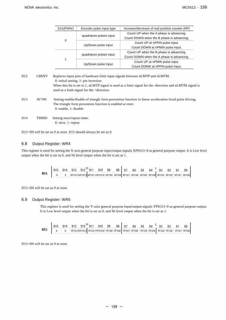
NOVA electronics Inc. MCX512 - 159
- 159 -
D11(PIINV) Encoder pulse input type Increase/decrease of real position counter (RP)
0 quadrature pulses input
Count UP when the A phase is advancing. Count DOWN when the B phase is advancing.
Up/Down pulse input Count UP at nPPIN pulse input.
Count DOWN at nPMIN pulse input.
1 quadrature pulses input
Count UP when the B phase is advancing. Count DOWN when the A phase is advancing.
Up/Down pulse input Count UP at nPMIN pulse input.
Count DONW at nPPIN pulse input.
D12 LMINV Replaces input pins of hardware limit input signals between nLMTP and nLMTM. 0: initial setting, 1: pin inversion When this bit is set to 1, nLMTP signal is used as a limit signal for the -direction and nLMTM signal is
used as a limit signal for the +direction.
D13 AVTRI Setting enable/disable of triangle form prevention function in linear acceleration fixed pulse driving. The triangle form prevention function is enabled at reset. 0: enable, 1: disable
D14 TMMD Setting once/repeat timer.
0: once, 1: repeat D15~D0 will be set as 0 at reset. D15 should always be set as 0.
6.8 Output Register: WR4
This register is used for setting the X-axis general purpose input/output signals XPIO13~0 as general purpose output. It is Low level output when the bit is set as 0, and Hi level output when the bit is set as 1.
D15~D0 will be set as 0 at reset.
6.9 Output Register: WR5
This register is used for setting the Y-axis general purpose input/output signals YPIO13~0 as general purpose output. It is Low level output when the bit is set as 0, and Hi level output when the bit is set as 1.
D15~D0 will be set as 0 at reset.
D7 D6 D5 D4H L
D15 D14 D13 D12 D11 D10 D9 D8 D3 D2 D1 D0WR4
XPIO0XPIO1XPIO2XPIO3XPIO4XPIO5XPIO6XPIO7XPIO8XPIO9XPIO10XPIO11XPIO12XPIO1300
D7 D6 D5 D4H L
D15 D14 D13 D12 D11 D10 D9 D8 D3 D2 D1 D0WR5 YPIO0YPIO1YPIO2YPIO3YPIO4YPIO5YPIO6YPIO7YPIO8YPIO9YPIO10YPIO11YPIO12YPIO1300
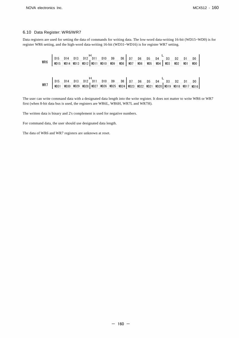
NOVA electronics Inc. MCX512 - 160
- 160 -
6.10 Data Register: WR6/WR7
Data registers are used for setting the data of commands for writing data. The low-word data-writing 16-bit (WD15~WD0) is for register WR6 setting, and the high-word data-writing 16-bit (WD31~WD16) is for register WR7 setting.
The user can write command data with a designated data length into the write register. It does not matter to write WR6 or WR7 first (when 8-bit data bus is used, the registers are WR6L, WR6H, WR7L and WR7H). The written data is binary and 2's complement is used for negative numbers. For command data, the user should use designated data length. The data of WR6 and WR7 registers are unknown at reset.
D7 D6 D5 D4H L
D15 D14 D13 D12 D11 D10 D9 D8 D3 D2 D1 D0WR6 WD0WD1WD2WD3WD4WD5WD6WD7WD8WD9WD10WD11WD12WD13WD14WD15
D7 D6 D5 D4H L
D15 D14 D13 D12 D11 D10 D9 D8 D3 D2 D1 D0WR7 WD16WD17WD18WD19WD20WD21WD22WD23WD24WD25WD26WD27WD28WD29WD30WD31

NOVA electronics Inc. MCX512 - 161
- 161 -
6.11 Main Status Register: RR0
Main status register is used for displaying the driving and error status of each axis. It also displays ready signal for continuous interpolation, quadrant of circular interpolation and continuous interpolation pre-buffer stack counter (SC).
D1~0 n-DRV Displaying driving status of each axis. When the bit is 1, the axis is outputting drive pulses, and when the bit
is 0, the driving of the axis is finished. During execution of automatic home search, this bit becomes 1. Once the in-position input signal nINPOS for servomotor is active, D1~0 bit will return to 0 after the drive
pulse output is finished. D5~4 n-ERR Displaying error status of each axis. If any of the error bits (D1~D0) of each axis RR2 register becomes 1, this bit will become 1. During driving except interpolation driving (including automatic home search), this bit will return to 0 by the
error/finishing status clear command (79h) or the start of next driving. When interpolation driving is performed, be sure to clear the error by the error/finishing status clear command (79h) after checking that interpolation drive stops. Otherwise, interpolation driving will not work properly after that.
D10~8 ZONEm Displaying the quadrant of the current position in circular interpolation.
D10 D9 D8 Quadrant
0 0 0 0 1 1 1 1
0 0 1 1 0 0 1 1
0 1 0 1 0 1 0 1
0 1 2 3 4 5 6 7
D11 CNEXT Displaying the writable state of next data for continuous interpolation. When interpolation driving is started, the bit becomes 1 during the period from 1 to 7 of pre-buffer stack
counter, and it is possible to write interpolation data for next node (parameters and interpolation commands).
D15~12 HSTC3~0 Displaying the value of continuous interpolation pre-buffer stack counter (SC).
D15 D14 D13 D12 Stack counter (SC)
0 0 0 0 0 0 0 0 1
0 0 0 0 1 1 1 1 0
0 0 1 1 0 0 1 1 0
0 1 0 1 0 1 0 1 0
0 1 2 3 4 5 6 7 8
During continuous interpolation driving, when SC is 8, it indicates the pre-buffer stack is the upper limit.
And when SC is 7 and under, it is possible to write interpolation data for next node (parameters and interpolation commands). When SC is 0, it indicates all the interpolation data was output and continuous interpolation driving is finished.
X-DRV
D7 D6 D5 D4H L
D15 D14 D13 D12 D11 D10 D9 D8 D3 D2 D1 D0RR0 Y-DRV00X-ERRY-ERR00ZONE0ZONE1ZONE2CNEXTHSTC0HSTC1HSTC2HSTC3
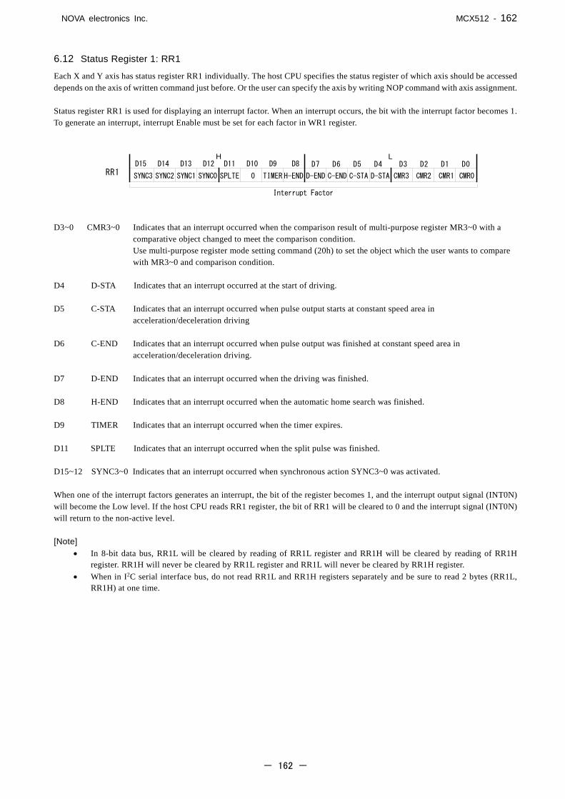
NOVA electronics Inc. MCX512 - 162
- 162 -
6.12 Status Register 1: RR1
Each X and Y axis has status register RR1 individually. The host CPU specifies the status register of which axis should be accessed depends on the axis of written command just before. Or the user can specify the axis by writing NOP command with axis assignment.
Status register RR1 is used for displaying an interrupt factor. When an interrupt occurs, the bit with the interrupt factor becomes 1. To generate an interrupt, interrupt Enable must be set for each factor in WR1 register.
D3~0 CMR3~0 Indicates that an interrupt occurred when the comparison result of multi-purpose register MR3~0 with a
comparative object changed to meet the comparison condition. Use multi-purpose register mode setting command (20h) to set the object which the user wants to compare
with MR3~0 and comparison condition. D4 D-STA Indicates that an interrupt occurred at the start of driving. D5 C-STA Indicates that an interrupt occurred when pulse output starts at constant speed area in
acceleration/deceleration driving D6 C-END Indicates that an interrupt occurred when pulse output was finished at constant speed area in
acceleration/deceleration driving. D7 D-END Indicates that an interrupt occurred when the driving was finished. D8 H-END Indicates that an interrupt occurred when the automatic home search was finished. D9 TIMER Indicates that an interrupt occurred when the timer expires. D11 SPLTE Indicates that an interrupt occurred when the split pulse was finished. D15~12 SYNC3~0 Indicates that an interrupt occurred when synchronous action SYNC3~0 was activated. When one of the interrupt factors generates an interrupt, the bit of the register becomes 1, and the interrupt output signal (INT0N) will become the Low level. If the host CPU reads RR1 register, the bit of RR1 will be cleared to 0 and the interrupt signal (INT0N) will return to the non-active level. [Note]
• In 8-bit data bus, RR1L will be cleared by reading of RR1L register and RR1H will be cleared by reading of RR1H register. RR1H will never be cleared by RR1L register and RR1L will never be cleared by RR1H register.
• When in I2C serial interface bus, do not read RR1L and RR1H registers separately and be sure to read 2 bytes (RR1L, RR1H) at one time.
D7 D6 D5 D4H L
D15 D14 D13 D12 D11 D10 D9 D8 D3 D2 D1 D0RR1 CMR1 CMR0CMR3 CMR2D-STAC-STAC-ENDD-ENDH-ENDTIMERSPLTESYNC0SYNC1SYNC2SYNC3
Interrupt Factor
0

NOVA electronics Inc. MCX512 - 163
- 163 -
6.13 Status Register 2: RR2
Each X and Y axis has status register RR2 individually. The host CPU specifies the status register of which axis should be accessed depends on the axis of written command just before. Or the user can specify the axis by writing NOP command with axis assignment. Status register RR2 is used for displaying the error information and the status of driving finishing. When an error occurs during the driving, the error information bit (one of D7 to D0) is set to 1. When one or more of D7 to D0 bits of RR2 register are 1, n-ERR bit of the axis in main status register RR0 becomes 1. When one or more bits of RR2 register are 1, the bits keep 1 even though the factor of the error or driving finishing is cleared. As for the error during driving except interpolation driving (including automatic home search), all bits will return to 0 by error/finishing status clear command (79h) or the start of next driving. And the error during interpolation driving, be sure to clear the error bit to 0 by error/finishing status clear command (79h) after checking that interpolation drive stops.
D0 SLMT+ During the +direction driving with software limit function enabled, when comparative position counter ≧ SLMT+ value, it becomes 1 and driving stops.
D1 SLMT- During the -direction driving with software limit function enabled, when comparative position counter <
SLMT- value, it becomes 1 and driving stops. D2 HLMT+ During the +direction driving with hardware limit signal enabled, when limit signal (nLMTP) is on its active
level, it becomes 1 and driving stops. D3 HLMT- During the -direction driving with hardware limit signal enabled, when limit signal (nLMTM) is on its active
level, it becomes 1 and driving stops. D4 ALARM During the driving with input signal for servo driver alarm enabled, when the alarm signal (nALARM) is on
its active level, it becomes 1 and driving stops. D5 EMG During the driving, when emergency stop signal (EMGN) becomes Low level, it becomes 1 and driving stops. D6 HOME Error occurred at execution of an automatic home search. When the encoder Z-phase signal (nSTOP2) is
already active at the start of Step 3, this bit is set to 1. D7 CERR Error related to continuous interpolation. It becomes 1 when writing of interpolation data for next node cannot
be finished during continuous interpolation driving and then driving stops. [Note]
• When hardware/software limit becomes active during driving, the decelerating stop or instant stop is executed. Unless the stop factor of driving is cleared, a driving command is not executed and an error occurs again even if a driving command in the same direction is written.
• The error information bits do not become 1 even if each factor is active during the stop of driving. About software/hardware limit, an error does not occur even if each factor becomes active in the reverse direction driving.
• When D7 bit becomes 1, be sure to write the error/finishing status clear command (79h) after checking that interpolation drive stops. Otherwise, interpolation driving will not work properly after that.
D8 SYNC If the driving is stopped by one of synchronous actions (SYNC3 ~ 0), it will become 1. D11~9 STOP2~0 If the driving is stopped by one of external stop signals (nSTOP2~ 0), it will become 1. D12 LMT+ If the driving is stopped by +direction limit signal (nLMTP), it will become 1.
SLMT+
D7 D6 D5 D4H L
D15 D14 D13 D12 D11 D10 D9 D8 D3 D2 D1 D0RR2 SLMT-HLMT+HLMT-ALARMEMGHOMECERRSYNCSTOP0STOP1STOP2LMTPLMTMALARMEMG
Error InformationStatus of Driving Finishing

NOVA electronics Inc. MCX512 - 164
- 164 -
D13 LMT- If the driving is stopped by -direction limit signal (nLMTM), it will become 1. D14 ALARM If the driving is stopped by nALARM from a servo driver, it will become 1. D15 EMG If the driving is stopped by external emergency signal (EMGN), it will become 1. Driving finishing status (D15~D8) is the bit indicates the finishing factor of driving. There are 3 factors that terminate driving as shown below other than the factors that the status of driving finishing (D15~D8) indicate. a. when all the drive pulses are output in fixed pulse driving, b. when deceleration stop or instant stop command is written, c. when software limit is enabled, and is active, Make sure to check the status of driving finishing (D15~D8) after confirming the driving is finished by the n-DRV bit of RR0 main status register.
6.14 Status Register 3: RR3
Each axis has status register RR3 individually. The host CPU specifies the status register of which axis should be accessed depends on the axis of written command just before. Or the user can specify the axis by writing NOP command with axis assignment.
Status register RR3 has 2 kinds of pages, Page 0 and Page1. Page 0 is used for displaying the input signal status and automatic home search execution state. Page 1 is used for displaying: (1). enable/disable of a synchronous action, (2). acceleration/deceleration status in acceleration/deceleration driving, (3). acceleration increasing/decreasing status in S-curve acceleration/deceleration, (4). timer operating state, (5). split pulse operating state. The page can be designated by writing RR3 Page Display Command (7Ah, 7Bh). It will be Page 0 at reset.
Page 0 The input signal status bit of each signal is 0 if the input is on the Low level and 1 if the input is on the Hi level. When the functions of D8~D0 input signals are not used, they can be used as general purpose input signals. In the descriptions below, the number in brackets after signal name indicates the pin number from X axis to Y axis in order. D2~0 STOP2~0 Displaying the input status of external stop signals nSTOP2 (69, 96), nSTOP1 (70, 97), nSTOP0 (71, 98). D3 ECA Displaying the input status of encoder input pulse signal nECA/PPIN (40, 42).
The pin number for this bit does not change even though the pin inversion of encoder pulse input (WR3/D11:PIINV) is set.
D4 ECB Displaying the input status of encoder input pulse signal nECB/PMIN (41, 43).
The pin number for this bit does not change even though the pin inversion of encoder pulse input (WR3/D11:PIINV) is set.
D5 INPOS Displaying the input status of in-position input signal for a servomotor nINPOS (65, 92). D6 ALARM Displaying the input status of servo alarm input signal nALARM (66, 93). D7 LMTP Displaying the input status of hardware limit input signal nLMTP (67, 94).
The pin number for this bit does not change even though the pin inversion of hardware limit input (WR3/D12:LMINV) is set.
STOP0
D7 D6 D5 D4H L
D15 D14 D13 D12 D11 D10 D9 D8 D3 D2 D1 D0RR3 Page0 STOP1STOP2ECAECBINPOSALARMLMTPLMTMHSST0HSST1HSST2HSST3HSST4HSST50
SYNC0
D7 D6 D5 D4H L
D15 D14 D13 D12 D11 D10 D9 D8 D3 D2 D1 D0
SYNC1SYNC2SYNC3ASNDCNSTDSNDAASNDACNSTADSNDTIMERSPLIT0001RR3 Page1

NOVA electronics Inc. MCX512 - 165
- 165 -
D8 LMTM Displaying the input status of hardware limit input signal nLMTM (98, 95). The pin number for this bit does not change even though the pin inversion of hardware limit input (WR3/D12:LMINV) is set.
D14~9 HSST5~0 The home search execution state indicates the operation currently executed while the automatic home search
is performed. See chapter 2.5.5. D15 PAGE Indicates RR3 is displaying Page 0 and becomes 0.
Page 1 D3~0 SYNC3~0 It becomes 1 when SYNC3~0 is active.
To enable a synchronous action, write a synchronous action enable command (8F~81h). To disable a synchronous action, write a synchronous action disable command (9F~91h).
D4 ASND It becomes 1 at acceleration area in
acceleration/deceleration driving. D5 CNST It becomes 1 at constant speed area in
acceleration/deceleration driving. D6 DSND It becomes 1 at deceleration area in
acceleration/deceleration driving. D7 AASND In S-curve, it becomes 1 when
acceleration/deceleration increases. D8 ACNST In S-curve, it becomes 1 when acceleration/deceleration keeps constant. D9 ADSND In S-curve, it becomes 1 when acceleration/deceleration decreases. D10 TIMER It becomes 1 when the timer is in operation. D11 SPLIT It becomes 1 when the split pulse is in operation. D15 PAGE Indicates RR3 is displaying Page 1 and becomes 1.
ASND=1 CNST=1 DSND=1
Speed
Time
Acceleration Deceleration
AASND=1 ACNST=1 ADSND=1 AASND=1 ACNST=1 ADSND=1
Acceleration/Deceleration

NOVA electronics Inc. MCX512 - 166
- 166 -
6.15 PIO Read Register 1: RR4
PIO read register RR4 is used for displaying the signal status of general purpose input/output signals XPIO13~0 in X axis. The bit is 0 if the signal is on the Low level; the bit is 1 if the signal is on the Hi level.
D13~0 XPIO13~0 Displaying the status of X axis general purpose input/output signals XPIO13~0.
When XPIO13~0 signals are set as input, it indicates the input state and when set as output, it indicates the output state.
6.16 PIO Read Register 2: RR5
PIO read register RR5 is used for displaying the signal status of general purpose input/output signals YPIO13~0 in Y axis. The bit is 0 if the signal is on the Low level; the bit is 1 if the signal is on the Hi level.
D13~0 YPIO13~0 Displaying the status of Y axis general purpose input/output signals YPIO13~0.
When YPIO13~0 signals are set as input, it indicates the input state and when set as output, it indicates the output state.
6.17 Data-Read Register: RR6/RR7
According to the data-read command, the data of internal registers will be set into registers RR6 and RR7. The low word 16 bits (RD15 ~ RD0) is set in RR6 register, and the high word 16 bits (RD31 ~ RD16) is set in RR7 register for data reading.
The data is binary and 2's complement is used for negative numbers.
D7 D6 D5 D4H L
D15 D14 D13 D12 D11 D10 D9 D8 D3 D2 D1 D0RR4 XPIO0XPIO1XPIO2XPIO3XPIO4XPIO5XPIO6XPIO7XPIO8XPIO9XPIO10XPIO11XPIO12XPIO1300
D7 D6 D5 D4H L
D15 D14 D13 D12 D11 D10 D9 D8 D3 D2 D1 D0RR5 YPIO0YPIO1YPIO2YPIO3YPIO4YPIO5YPIO6YPIO7YPIO8YPIO9YPIO10YPIO11YPIO12YPIO1300
D7 D6 D5 D4H L
D15 D14 D13 D12 D11 D10 D9 D8 D3 D2 D1 D0RR6 RD0RD1RD2RD3RD4RD5RD6RD7RD8RD9RD10RD11RD12RD13RD14RD15
D7 D6 D5 D4H L
D15 D14 D13 D12 D11 D10 D9 D8 D3 D2 D1 D0RR7 RD16RD17RD18RD19RD20RD21RD22RD23RD24RD25RD26RD27RD28RD29RD30RD31

NOVA electronics Inc. MCX512 - 167
- 167 -
7. Commands
7.1 Command Lists
Commands for Writing Data
Code Command Symbol Data Range Data Length
(byte)
00h Jerk setting (Acceleration increasing rate)
JK 1 ~ 1,073,741,823 [pps/sec2] 4
01 Deceleration increasing rate setting
DJ 1 ~ 1,073,741,823 [pps/sec2] 4
02 Acceleration setting AC 1 ~ 536,870,911 [pps/sec] 4
03 Deceleration setting DC 1 ~ 536,870,911 [pps/sec] 4
04 Initial speed setting SV 1 ~ 8,000,000 [pps] 4
05 Drive speed setting DV 1 ~ 8,000,000 [pps] 4
06 Drive pulse number/ Finish point setting
TP -2,147,483,646 ~ +2,147,483,646 4
07 Manual deceleration point setting
DP 0 ~ 4,294,967,292 4
08 Circular center point setting CP -2,147,483,646 ~ +2,147,483,646 4
09 Logical position counter setting LP -2,147,483,648 ~ +2,147,483,647 4
0A Real position counter setting RP -2,147,483,648 ~ +2,147,483,647 4
0B Software limit + setting SP -2,147,483,647 ~ +2,147,483,647 4
0C Software limit − setting SM -2,147,483,647 ~ +2,147,483,647 4
0D Acceleration counter offsetting AO -32,768 ~ +32,767 2
0E Logical position counter maximum value setting
LX 1 ~ 2,147,483,647(7FFF FFFFh)
Or FFFF FFFFh 4
0F Real position counter maximum value setting
RX 1 ~ 2,147,483,647(7FFF FFFFh)
Or FFFF FFFFh 4
10 Multi-purpose register 0 setting MR0 -2,147,483,648 ~ +2,147,483,647 4
11 Multi-purpose register 1 setting MR1 -2,147,483,648 ~ +2,147,483,647 4
12 Multi-purpose register 2 setting MR2 -2,147,483,648 ~ +2,147,483,647 4
13 Multi-purpose register 3 setting MR3 -2,147,483,648 ~ +2,147,483,647 4
14 Home search speed setting HV 1 ~ 8,000,000 [pps] 4
15 Speed increasing/decreasing value setting
IV 1 ~ 1,000,000 [pps] 4
16 Timer value setting TM 1 ~ 2,147,483,647 [μsec] 4
17 Split pulse setting 1 SP1 Split length:2 ~ 65,535
Pulse width:1 ~ 65,534 4
18 Split pulse setting 2 SP2 Split pulse number:0 ~ 65,535 2
19 Interpolation/Finish point maximum value setting
TX 1~2,147,483,646 4
[Note] • When parameters are written, the total data length should be completely filled. • The units described in speed parameters and the timer value are only applied to when input clock (CLK) is 16MHz. When
input clock (CLK) is other than 16MHz, please see Appendix B for parameter calculation formula.

NOVA electronics Inc. MCX512 - 168
- 168 -
Commands for Writing Mode
Code Command Symbol Data Length
(byte) 20h Multi-purpose register mode setting MRM 2
21 PIO signal setting 1 P1M 2
22 PIO signal setting 2・Other settings P2M 2
23 Automatic home search mode setting 1 H1M 2
24 Automatic home search mode setting 2 H2M 2
25 Input signal filter mode setting FLM 2
26 Synchronous action SYNC0 setting S0M 2
27 Synchronous action SYNC1 setting S1M 2
28 Synchronous action SYNC2 setting S2M 2
29 Synchronous action SYNC3 setting S3M 2
2A Interpolation mode setting IPM 2
2B PIO signal setting 3 P3M 2
[Note] When parameters are written, the total data length should be completely filled.
Commands for Reading Data
Code Command Symbol Data Range Data Length
(byte) 30h Logical position counter reading LP -2,147,483,648 ~ +2,147,483,647 4
31 Real position counter reading RP -2,147,483,648 ~ +2,147,483,647 4
32 Current drive speed reading CV 0 ~ 8,000,000 [pps] 4
33 Current acceleration/deceleration reading
CA 0 ~ 536,870,911 [pps/sec] 4
34 Multi-purpose register 0 reading MR0 -2,147,483,648 ~ +2,147,483,647 4
35 Multi-purpose register 1 reading MR1 -2,147,483,648 ~ +2,147,483,647 4
36 Multi-purpose register 2 reading MR2 -2,147,483,648 ~ +2,147,483,647 4
37 Multi-purpose register 3 reading MR3 -2,147,483,648 ~ +2,147,483,647 4
38 Current timer value reading CT 0 ~ 2,147,483,647 [μsec] 4
39 Interpolation/Finish point maximum value reading
TX 0~2,147,483,646 4
3D WR1 setting value reading WR1 (bit data) 2
3E WR2 setting value reading WR2 (bit data) 2
3F WR3 setting value reading WR3 (bit data) 2
40 Multi-purpose register mode setting reading
MRM (bit data) 2
41 PIO signal setting 1 reading P1M (bit data) 2
42 PIO signal setting 2/Other settings reading
P2M (bit data) 2
43 Acceleration setting value reading AC 1 ~ 536,870,911 [pps/sec] 4
44 Initial speed setting value reading SV 1 ~ 8,000,000 [pps] 4
45 Drive speed setting value reading DV 1 ~ 8,000,000 [pps] 4
46 Drive pulse number/Finish point setting value reading
TP -2,147,483,646 ~ +2,147,483,646 4
47 Split pulse setting 1 reading SP1 Split length:2 ~ 65,535
Pulse width:1 ~ 65,534 4
48 General purpose input value reading UI RR6: 2 bytes (D15~0 in I2C communication) 4
49 PIO signal setting 3 reading P3M (bit data) 2

NOVA electronics Inc. MCX512 - 169
- 169 -
Driving Commands
Code Command 50h Relative position driving 51 Counter relative position driving 52 + Direction continuous pulse driving 53 - Direction continuous pulse driving 54 Absolute position driving 56 Decelerating stop 57 Instant stop 58 Direction signal + setting 59 Direction signal - setting 5A Automatic home search execution
Interpolation Commands
Code Command 61h 2-axis linear interpolation driving 64 CW circular interpolation driving 65 CCW circular interpolation driving 66 2-axis bit pattern interpolation driving 6D Deceleration enabling 6E Deceleration disabling 6F Interpolation interrupt clear/Single-step interpolation
Synchronous Action Operation Commands
Code Command
81~8Fh Synchronous action enable setting 91~9F Synchronous action disable setting A1~AF Synchronous action activation
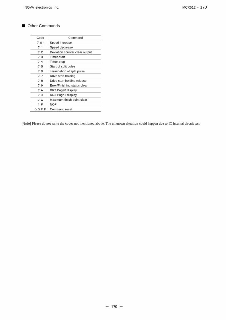
NOVA electronics Inc. MCX512 - 170
- 170 -
Other Commands
Code Command 70h Speed increase 71 Speed decrease 72 Deviation counter clear output 73 Timer-start 74 Timer-stop 75 Start of split pulse 76 Termination of split pulse 77 Drive start holding 78 Drive start holding release 79 Error/Finishing status clear 7A RR3 Page0 display 7B RR3 Page1 display 7C Maximum finish point clear 1F NOP
00FF Command reset [Note] Please do not write the codes not mentioned above. The unknown situation could happen due to IC internal circuit test.

NOVA electronics Inc. MCX512 - 171
- 171 -
7.2 Commands for Writing Data
Commands for writing data is used for setting driving parameters such as acceleration, drive speed, drive pulse number… When more than one axis is specified, it is possible to set the same data in specified axes simultaneously. If the data length is 2 bytes, WR6 register can be used. If the data is 4 bytes, the high word data can be written into register WR7 and the low word into register WR6. Then, the axis assignment and command code will be written into register WR0 for execution. Writing data for registers WR6 and WR7 is binary and 2's complement is used for negative numbers. Each data should be set within the permitted data range. If the setting data is out of range, operation cannot be done correctly. [Note]
• It requires 125 nSEC (maximum) to access the command code when CLK=16MHz. Please do not write the next command or data during the period of time.
• Except acceleration offset (AO), logical position counter maximum value (LX) and real position counter maximum value (RX), other parameters are unknown at reset. So, please set proper values for those driving related parameters before the driving starts.
• The unit described in each speed parameter and timer value is for when input clock (CLK) is 16MHz. Please see Appendix B for parameter calculation formula when input clock (CLK) is other than 16MHz.
7.2.1 Jerk Setting
Code Command Symbol Data Range Data Length (byte)
00h Jerk setting JK 1 ~ 1,073,741,823 4
A jerk setting value is a parameter that determines the acceleration increasing/decreasing rate per unit in S-curve acceleration/deceleration. The unit of the setting value is pps/sec2.
Jerk = JK [pps/sec2] In S-curve acceleration/deceleration driving (WR3/D1=0) where acceleration and deceleration are symmetrical, this jerk is also used at deceleration.
7.2.2 Deceleration Increasing Rate Setting
Code Command Symbol Data Range Data Length (byte)
01h Deceleration Increasing Rate Setting DJ 1 ~ 1,073,741,823 4
This deceleration increasing rate value is a parameter used to determine a deceleration speed increase/decrease rate per unit time in S-curve acceleration/deceleration driving (WR3/D1= 1) where acceleration and deceleration are non-symmetrical. The unit of the setting value is pps/sec2.
Deceleration Increasing Rate = DJ [pps/sec2] In S-curve acceleration/deceleration driving (WR3/D1=0) where acceleration and deceleration are symmetrical, the deceleration increasing rate value is not used.

NOVA electronics Inc. MCX512 - 172
- 172 -
7.2.3 Acceleration Setting
Code Command Symbol Data Range Data Length (byte)
02h Acceleration setting AC 1 ~ 536,870,911 4
An acceleration setting value is a parameter that determines acceleration in linear acceleration/deceleration driving. The unit of the setting value is pps/sec.
Acceleration = AC [pps/sec] In linear acceleration/deceleration driving (WR3/D1=0) where acceleration and deceleration are symmetrical, this acceleration setting value is also used at deceleration. For S-curve acceleration/deceleration driving, set the maximum value of 536,870,911 (1FFF FFFFh) to this parameter. For Partial S-curve acceleration/deceleration driving, set the acceleration at linear acceleration part to this parameter. In Partial S-curve acceleration/deceleration driving (WR3/D1=0) where acceleration and deceleration are symmetrical, this acceleration setting value is also used at deceleration. The value of current acceleration can be read by current acceleration/deceleration reading command (33h). An acceleration setting value can be read by acceleration setting value reading command (43h).
7.2.4 Deceleration Setting
Code Command Symbol Data Range Data Length (byte)
03h Deceleration setting DC 1 ~ 536,870,911 4
This parameter is used to set a deceleration speed at deceleration in non-symmetrical linear acceleration/deceleration driving (WR3/D1=1). The unit of the setting value is pps/sec.
Deceleration = DC [pps/sec] In non-symmetrical S-curve acceleration/deceleration driving, set the maximum value of 536,870,911(1FFF FFFFh)to this parameter. In non-symmetrical Partial S-curve acceleration/deceleration driving, set the deceleration at linear deceleration part to this parameter.

NOVA electronics Inc. MCX512 - 173
- 173 -
7.2.5 Initial Speed Setting
Code Command Symbol Data Range Data Length (byte)
04h Initial speed setting SV 1 ~ 8,000,000 4
“SV” is the parameter determining the initial speed for the start of acceleration and the termination of deceleration. The unit of the setting value is pps.
Initial Speed = SV [pps] For a stepper motor, the user should set the initial speed smaller than the self-starting frequency of a stepper motor. If there is the mechanical resonance frequency, set the initial speed to avoid it. In fixed pulse driving, if the value which is too low is set to initial speed, premature termination or creep pulses may occur.
・ In linear acceleration/deceleration driving, set the value more than square root of an acceleration setting value. ・ In S-curve acceleration/deceleration driving, set the value more than 1/10 times the square root of a jerk setting value. ・ In Partial S-curve acceleration/deceleration driving, set the value more than square root of an acceleration setting value.
Linear acceleration/deceleration driving ACSV≧ , S-curve acceleration/deceleration driving 1/10JK≧SV × ,
Partial S-curve acceleration/deceleration driving ACSV≧
An initial speed setting value can be read by initial speed setting value reading command (44h).
7.2.6 Drive Speed Setting
Code Command Symbol Data Range Data Length (byte)
05h Drive speed setting DV 1 ~ 8,000,000 4
“DV” is the parameter determining the speed of constant speed period in trapezoidal driving. In constant speed driving, the drive speed is the initial speed. The unit of the setting value is pps.
Drive speed = DV [pps] If the drive speed is set a lower value than the initial speed, the acceleration/deceleration will not be performed, and the driving is constant speed. If the user wants to perform instant stop immediately after the signal is detected during such as the encoder Z-phase search (at a low-speed driving), the drive speed must be set lower than the initial speed. A drive speed can be altered during the driving. When the drive speed of next constant speed period is newly set, the acceleration or deceleration is performed to reach the new setting speed, then a constant speed driving starts. In automatic home search, this drive speed is used for high-speed search speed of Step 1 and high-speed drive speed of Step 4. [Note]
• In fixed pulse S-curve acceleration/deceleration driving (when in auto deceleration mode) or in fixed pulse non-symmetrical linear acceleration/deceleration driving (when in auto deceleration mode), there is no way to change the drive speed during the driving.
• In continuous S-curve acceleration/deceleration driving, the drive speed can be changed in the constant speed period during the driving, but changing the drive speed during the acceleration/deceleration will be disabled.
• In fixed pulse symmetrical trapezoidal driving, the drive speed can be changed during the driving, however the frequent changes of drive speed may generate premature termination or creep.
• The drive speed can be changed during interpolation driving by synchronous action. The value of current drive speed during the driving can be read by current drive speed reading command (32h). A drive speed setting value can be read by drive speed setting value reading command (45h).

NOVA electronics Inc. MCX512 - 174
- 174 -
7.2.7 Drive pulse number / Finish point setting
Code Command Symbol Data Range Data Length (byte)
06h Drive pulse number/finish point setting TP -2,147,483,646 ~ +2,147,483,646 4
“TP” is the parameter setting the drive pulse number from the current position for relative position driving. When the positive pulse number is set in the drive pulse number, a drive direction is toward +direction, and when the negative pulse number is set, a drive direction is toward -direction. In counter relative position driving, when the positive pulse number is set in the drive pulse number, a drive direction is toward -direction. In absolute position driving, the destination point based on a home (logical position counter = 0) should be set with a signed 32-bit value. Drive pulse number can be changed during relative position driving or counter relative position driving. However, it cannot be set to a different drive direction. Please note that if it is set to the position already passed, driving will stop immediately. The finish point cannot be changed during absolute position driving. In linear and circular interpolation driving, it sets the finish point of each axis. The finish point should be set the relative value to the current position with a signed 32-bit value. In bit pattern interpolation driving, it sets the bit data of each axis. The lower 16 bits of 32 bits are used to set +direction bit data and the upper 16 bits are used to set -direction bit data.
7.2.8 Manual Decelerating Point Setting
Code Command Symbol Data Range Data Length (byte)
07h Manual decelerating point setting DP 0 ~ 4,294,967,292 4
“DP” is the parameter setting the manual deceleration point in fixed pulse acceleration/deceleration driving when the manual deceleration mode (WR3/D0=1) is engaged. As a manual decelerating point, set the value which subtracts pulse number to be used at deceleration from output pulse number in fixed pulse driving.
Manual Decelerating Point = Output Pulse Number − Pulse Number for Deceleration <About output pulse number> Output pulse number indicates the number of pulses which is actually output in fixed pulse driving. In relative position driving, output pulse number P is the absolute value of drive pulse number setting value TP. In absolute position driving, output pulse number P is the absolute value which reduces logical position counter value LP of before driving starts from drive pulse number setting value TP.
Relative Position Driving :Output Pulse Number P = | TP | Absolute Position Driving :Output Pulse Number P = | TP - LP |

NOVA electronics Inc. MCX512 - 175
- 175 -
7.2.9 Circular Center Point Setting
Code Command Symbol Data Range Data Length (byte)
08h Circular center point setting CT -2,147,483,648 ~ +2,147,483,647 4
“CT” is the parameter setting the center point in circular driving. The coordinates of center point should be set the signed relative value to the current position.
7.2.10 Logical Position Counter Setting
Code Command Symbol Data Range Data Length (byte)
09h Logical position counter setting LP -2,147,483,648 ~ +2,147,483,647 4
“LP” is the parameter setting the value of logical position counter. Logical position counter counts Up/Down according to the +/- direction pulse output. A logical position counter setting value can be written anytime, and read by logical position counter reading command (30h) anytime.
7.2.11 Real Position Counter Setting
Code Command Symbol Data Range Data Length (byte)
0Ah Real position counter setting RP -2,147,483,648 ~ +2,147,483,647 4
“RP” is the parameter setting the value of real position counter. Real position counter counts Up/Down according to encoder input pulse. A real position counter setting value can be written anytime, and read by real position counter reading command (31h) anytime.
7.2.12 Software Limit + Setting
Code Command Symbol Data Range Data Length (byte)
0Bh Software limit + setting SP -2,147,483,647 ~ +2,147,483,647 4
“SP” is the parameter setting the value of +direction software limit SLMT+ register. Enable/disable, an object to set, and stop mode of software limit can be set by WR2 register. A software limit SLMT+ register setting value can be written anytime.

NOVA electronics Inc. MCX512 - 176
- 176 -
7.2.13 Software Limit − Setting
Code Command Symbol Data Range Data Length (byte)
0Ch Software limit - setting SM -2,147,483,647 ~ +2,147,483,647 4
“SM” is the parameter setting the value of -direction software limit SLMT- register. Enable/disable, an object to set, and stop mode of software limit can be set by WR2 register. A software limit SLMT- register setting value can be written anytime.
7.2.14 Acceleration Counter Offsetting
Code Command Symbol Data Range Data Length (byte)
0Dh Acceleration Counter Offsetting AO -32,768 ~ +32,767 2
“AO” is the parameter executing acceleration counter offset. The offset value of acceleration counter will be set to 0 at reset. There is usually no need to change it. See chapter 2.1 [ Offset Setting for Acceleration/Deceleration Driving] for details of acceleration counter offsetting. The data length of this writing command is 2 bytes. The setting value should only be written into WR6 register.
7.2.15 Logical Position Counter Maximum Value Setting
Code Command Symbol Data Range Data Length (byte)
0Eh Logical position counter maximum value setting
LX 1 ~ 2,147,483,647(7FFF FFFFh)
Or FFFF FFFFh 4
“LX” is the parameter setting the logical position counter maximum value with positive value for the variable ring function of logical position counter. The value at reset is FFFF FFFFh. When the variable ring function is not used, the value should be default.
7.2.16 Real Position Counter Maximum Value Setting
Code Command Symbol Data Range Data Length (byte)
0Fh Real position counter maximum value setting
RX 1 ~ 2,147,483,647(7FFF FFFFh)
Or FFFF FFFFh 4
“RX” is the parameter setting the real position counter maximum value with positive value for the variable ring function of real position counter. The value at reset is FFFF FFFFh. When the variable ring function is not used, the value should be default.

NOVA electronics Inc. MCX512 - 177
- 177 -
7.2.17 Multi-Purpose Register 0 Setting
Code Command Symbol Data Range Data Length (byte)
10h Multi-purpose register 0 setting MR0 -2,147,483,648 ~ +2,147,483,647 4
“MR0” is the parameter setting the value of multi-purpose register 0. Multi-purpose register is used for comparison of position, speed, timer value and large or small, and load/save of each parameter as a synchronous action. Comparison result is used for comparative signal output, synchronous action activation and generating an interrupt. A multi-purpose register MR0 setting value can be written anytime, and read by multi-purpose register 0 reading command (34h) anytime.
7.2.18 Multi-Purpose Register 1 Setting
Code Command Symbol Data Range Data Length (byte)
11h Multi-purpose register 1 setting MR1 -2,147,483,648 ~ +2,147,483,647 4
“MR1” is the parameter setting the value of multi-purpose register 1. Multi-purpose register is used for comparison of position, speed, timer value and large or small, and load/save of each parameter as a synchronous action. Comparison result is used for outputting of comparison output signal, synchronous action activation and generating an interrupt. A multi-purpose register MR1 setting value can be written anytime, and read by multi-purpose register 1 reading command (35h) anytime.
7.2.19 Multi-Purpose Register 2 Setting
Code Command Symbol Data Range Data Length (byte)
12h Multi-purpose register 2 setting MR2 -2,147,483,648 ~ +2,147,483,647 4
“MR2” is the parameter setting the value of multi-purpose register 2. Multi-purpose register is used for comparison of position, speed, timer value and large or small, and load/save of each parameter as a synchronous action. Comparison result is used for outputting of comparison output signal, synchronous action activation and generating an interrupt. A multi-purpose register MR2 setting value can be written anytime, and read by multi-purpose register 2 reading command (36h) anytime.

NOVA electronics Inc. MCX512 - 178
- 178 -
7.2.20 Multi-Purpose Register 3 Setting
Code Command Symbol Data Range Data Length (byte)
13h Multi-purpose register 3 setting MR3 -2,147,483,648 ~ +2,147,483,647 4
“MR3” is the parameter setting the value of multi-purpose register 3. Multi-purpose register is used for comparison of position, speed, timer value and large or small, and load/save of each parameter as a synchronous action. Comparison result is used for outputting of comparison output signal, synchronous action activation and generating an interrupt. A multi-purpose register MR3 setting value can be written anytime, and read by multi-purpose register 3 reading command (37h) anytime.
7.2.21 Home Search Speed Setting
Code Command Symbol Data Range Data Length (byte)
14h Home search speed setting HV 1 ~ 8,000,000 4
“HV” is the parameter setting the low-speed home search speed that is applied in Steps 2 and 3. The unit of the setting value is pps.
Home Search Speed = HV [pps] Set a value lower than the initial speed (SV) to stop driving immediately when a search signal becomes active. See chapter 2.5 for details of automatic home search.
7.2.22 Speed Increasing/Decreasing Value Setting
Code Command Symbol Data Range Data Length (byte)
15h Speed increasing/decreasing value setting IV 1 ~ 1,000,000 4
“IV” is the parameter setting the value to increase/decrease the current drive speed by speed increase command (70h) and speed decrease command (71h) during the driving. The unit of the setting value is pps.
Speed Increasing/Decreasing Value = IV [pps] In acceleration/deceleration driving, the speed increase/decrease command is written at constant speed area, acceleration/deceleration is performed until it reaches the drive speed by this speed increasing/decreasing value setting, and then constant speed driving will start again.

NOVA electronics Inc. MCX512 - 179
- 179 -
7.2.23 Timer Value Setting
Code Command Symbol Data Range Data Length (byte)
16h Timer value setting TM 1 ~ 2,147,483,647 4
“TM” is the parameter setting the time that a timer is up. The unit of the setting value is μsec.
Timer Value = TM [μsec] The current timer value during the timer operation can be read by current timer value reading command (38h).
7.2.24 Split Pulse Setting 1
Code Command Symbol Data Range Data Length (byte)
17h Split pulse setting 1 SP1 WR6 Split length:2 ~ 65,535
4 WR7 Pulse width:1 ~ 65,534
“SP1” is the parameter setting a split length and pulse width of a split pulse. The unit of split length and pulse width is drive pulse. Set a split length to WR6 and pulse width to WR7. Split length and pulse width can be altered during output of split pulse. When split length and pulse width are newly set, output of split pulse will continue at the new settings. This data length is 4 bytes, so even if only one of split length and pulse width is altered, the appropriate data should be set in both WR6 and WR7 registers. The value of split pulse setting 1 (SP1) can be read by split pulse setting 1 reading command (47h).
7.2.25 Split Pulse Setting 2
Code Command Symbol Data Range Data Length (byte)
18h Split pulse setting 2 SP2 Split pulse number:0,1 ~ 65,535 2
“SP2” is the parameter setting the split pulse number to output. When the split pulse number is set to 0, it continues to output split
pulses until the output of split pulse is stopped by a command or synchronous action. The split pulse number can be altered during output of split pulse. This data length is 2 bytes, the setting data should be written into WR6 register.

NOVA electronics Inc. MCX512 - 180
- 180 -
7.2.26 Interpolation/Finish Point Maximum Value Setting
Code Command Symbol Data Range Data Length (byte)
19h Interpolation/Finish point maximum value setting
TX 1~2,147,483,646 4
“TX” is the parameter setting the maximum value of finish point in linear interpolation. It does not require axis assignment, and should be set with an unsigned 32-bit value. The linear interpolation is calculated based on the value set by this command. When using this command, the linear interpolation maximum value must be manually set by interpolation mode setting command (2Ah).

NOVA electronics Inc. MCX512 - 181
- 181 -
7.3 Commands for Writing Mode
Commands for writing mode is used for setting driving parameters such as multi-purpose register, automatic home search, synchronous action and interpolation driving. When more than one axis is specified, it is possible to set the same data in specified axes simultaneously. Interpolation mode setting does not need axis assignment. The data length of commands for writing mode is all 2 bytes. Set an appropriate value in each bit of WR6 register and write a command code into WR0 register. As a result, the data of WR6 register will be set to each mode setting register in the IC. At reset, all the bits of each mode setting register in the IC are cleared to 0. [Note]
• It requires 125 nSEC (maximum) to access the command code when CLK=16MHz. Please do not write the next command or data during the period of time.
7.3.1 Multi-Purpose Register Mode Setting
Code Command Symbol Data Length (byte)
20h Multi-purpose register mode setting MRM 2
“MRM” is the parameter setting the comparative object with multi-purpose register MR3~0 and the comparison condition. The user can set the comparative object and comparison condition for each MR3~0 individually. Comparison result can be used for comparative signal output, the factor of synchronous action activation and an interrupt.
D1, 0 M0T1, 0 Setting the comparative object with MR0. D3, 2 M0C1, 0 Setting the comparison condition with MR0. D5, 4 M1T1, 0 Setting the comparative object with MR1. D7, 6 M1C1, 0 Setting the comparison condition with MR1 D9, 8 M2T1, 0 Setting the comparative object with MR2. D11, 10 M2C1, 0 Setting the comparison condition with MR2. D13, 12 M3T1, 0 Setting the comparative object with MR3. D15, 14 M3C1, 0 Setting the comparison condition with MR3.
Regardless of the comparison condition (MnC1, 0 bits) set by multi-purpose register mode setting, MR3~0 and the comparison result of large or small with each comparative object can be checked by RR4 register. See chapter 2.4 for details of multi-purpose register.
[Note] • When the comparative object is set to “current drive speed value (CV)” and comparison condition is set to “comparative
object =MRm”, if the acceleration/deceleration exceeds 4,194,304 (400000h) pps/sec in acceleration/deceleration driving, the comparison result may not become active. When the comparative object is “current drive speed value (CV)” and the acceleration/deceleration is more than this value, set the other conditions such as “comparative object ≧M Rm” and not “comparative object =MRm”.
D15~D0 will be set to 0 at reset.
WR6D7 D6 D5 D4
H LD15 D14 D13 D12 D11 D10 D9 D8 D3 D2 D1 D0
M0T0M0T1M0C0M0C1M1T0M1T1M1C0M2T0 M1C1M2T1M2C0M2C1M3T1 M3T0M3C0M3C1
MR0comparative
object
MR0comparison
condition
MR1comparative
object
MR1comparison
condition
MR2comparative
object
MR2comparison
condition
MR3comparative
object
MR3comparison
condition
MkT1 bit MkT0 bit MRm comparative object 0 0 Logical position counter (LP) 0 1 Real position counter (RP) 1 0 Current drive speed value (CV) 1 1 Current timer value (CT)
MkC1 bit MkC0 bit MRm comparison condition 0 0 comparative object ≧ MRm
0 1 comparative object > MRm 1 0 comparative object = MRm 1 1 comparative object < MRm
(k:0~3)
(k:0~3)

NOVA electronics Inc. MCX512 - 182
- 182 -
7.3.2 PIO Signal Setting 1
Code Command Symbol Data Length (byte)
21h PIO signal setting 1 P1M 2
“P1M” is the parameter setting the function of nPIO7~0 signals. nPIO7~0 signals can be used for the general purpose input/output signals, synchronous input signals, synchronous pulse output signals, drive status output signals, MRm comparison output signals and driving by external signals.
D1, 0 P0M1, 0 Setting the nPIO0 signal function. D3, 2 P1M1, 0 Setting the nPIO1 signal function. D5, 4 P2M1, 0 Setting the nPIO2 signal function. D7, 6 P3M1, 0 Setting the nPIO3 signal function. D9, 8 P4M1, 0 Setting the nPIO4 signal function. D11, 10 P5M1, 0 Setting the nPIO5 signal function. D13, 12 P6M1, 0 Setting the nPIO6 signal function. D15, 14 P7M1, 0 Setting the nPIO7 signal function. Each function is shown as follows.
(k:0~7)
PkM1 bit PkM0 bit Function
0 0
General purpose input nPIO7~0 signals become an input state. The signal level of each axis can be read by the following register: X axis from D7~0 of RR4, Y axis from D7~0 of RR5 register. In synchronous action, it can be activated by the signals ↑ or ↓. In driving by external signals, relative position driving or continuous pulse driving can be activated by nPIO4, 5 signals.
0 1
General purpose output nPIO7~0 signals become an output state. The values of WR4, 5 registers are output to the following bit of each axis respectively: D7~0 of WR4 are output to PIO7~0 of X axis, D7~0 of WR5 to PIO7~0 of Y axis. When the value is 0, it is Low level output and when is 1, it is Hi level output.
1 0 Drive status output
nPIO7~0 signals become an output state and each signal outputs the drive status as shown in the following table.
1 1
Synchronous pulse・MRm comparison output nPIO7~0 signals become an output state. nPIO3~0 output synchronous pulses and nPIO7~4 output MRm comparison value. The comparative object and comparison condition can be set by multi-purpose register mode setting command (20h).
WR6D7 D6 D5 D4
H LD15 D14 D13 D12 D11 D10 D9 D8 D3 D2 D1 D0
P1M0 P0M1P2M0P3M0 P0M0P1M1P2M1P3M1
nPIO0signal
nPIO1signal
nPIO2signal
nPIO3signal
P4M0P5M0P6M0P7M0 P4M1P5M1P6M1P7M1
nPIO4signal
nPIO5signal
nPIO6signal
nPIO7signal

NOVA electronics Inc. MCX512 - 183
- 183 -
The function of each nPIOm signal is shown as follows.
(K: 0~7)
nPIOm Signal (Pin Number)
PkM1,0 = 0,0 PkM1,0 = 0,1 PkM1,0 = 1,0 PkM1,0 = 1,1
General Purpose Input *Note
General Purpose Output
Drive Status Output
(True = Hi)
Synchronous Pulse Output, MRm Comparison Output
XPIO0(62) YPIO0(87)
X axis:RR4/D0 Y axis:RR5/D80
signal level reading
X axis:WR4/D0 Y axis:WR5/D0 value output
Driving SYNC0
Synchronous pulse output
XPIO1(61) YPIO1(86)
X axis:RR4/D1 Y axis:RR5/D1
signal level reading
X axis:WR4/D1 Y axis:WR5/D1 value output
Error SYNC1
Synchronous pulse output
XPIO2(60) YPIO2(85)
X axis:RR4/D2 Y axis:RR5/D2
signal level reading
X axis:WR4/D2 Y axis:WR5/D2 value output
Accelerating SYNC2
Synchronous pulse output
XPIO3(57) YPIO3(84)
X axis:RR4/D3 Y axis:RR5/D3
signal level reading
X axis:WR4/D3 Y axis:WR5/D3 value output
Constant speed driving
SYNC3 Synchronous pulse output
XPIO4(56) YPIO4(83)
X axis:RR4/D4 Y axis:RR5/D4
signal level reading
X axis:WR4/D4 Y axis:WR5/D4 value output
Decelerating MR0 comparison output
(True = Hi)
XPIO5(55) YPIO5(82)
X axis:RR4/D5 Y axis:RR5/D5
signal level reading
X axis:WR4/D5 Y axis:WR5/D5 value output
Acceleration increasing
MR1 comparison output (True = Hi)
XPIO6(54) YPIO6(81)
X axis:RR4/D6 Y axis:RR5/D6
signal level reading
X axis:WR4/D6 Y axis:WR5/D6 value output
Acceleration Constant
MR2 comparison output (True = Hi)
XPIO7(53) YPIO7(80)
X axis:RR4/D7 Y axis:RR5/D7
signal level reading
X axis:WR4/D7 Y axis:
WR5/D67 value output
Acceleration decreasing
MR3 comparison output (True = Hi)
See chapter 2.8 General Purpose Input/Output Signals for details of nPIO7~0 signals. [Note]
• When nPIO7~0 signals are general purpose input mode (PkM1, 0 = 0, 0), it can be used as activation factor of a synchronous action. See chapter 2.6 for more details.
• When nPIO4, 5 signals are general purpose input mode (PkM1, 0 = 0, 0), it can be used as input signals (nEXPP, nEXPM input) for driving by external signals. See chapter 2.12.1 for more details.
D15~D0 will be set as 0 at reset.
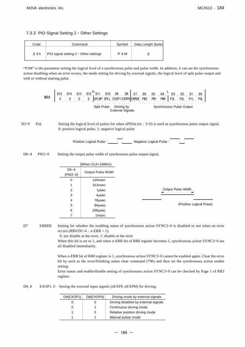
NOVA electronics Inc. MCX512 - 184
- 184 -
7.3.3 PIO Signal Setting 2・Other Settings
Code Command Symbol Data Length (byte)
22h PIO signal setting 2・Other settings P2M 2
“P2M” is the parameter setting the logical level of a synchronous pulse and pulse width. In addition, it can set the synchronous action disabling when an error occurs, the mode setting for driving by external signals, the logical level of split pulse output and with or without starting pulse.
D3~0 PnL Setting the logical level of pulses for when nPIOm (m:3~0) is used as synchronous pulse output signal. 0: positive logical pulse, 1: negative logical pulse
D6~4 PW2~0 Setting the output pulse width of synchronous pulse output signal.
(When CLK=16MHz) D6~4
(PW2~0) Output Pulse Width
0 125nsec 1 312nsec 2 1μsec 3 4μsec 4 16μsec 5 64μsec 6 256μsec 7 1msec
D7 ERRDE Setting for whether the enabling status of synchronous action SYNC3~0 is disabled or not when an error
occurs (RR0/D5~4:n-ERR = 1). 0: not disable at the error, 1: disable at the error When this bit is set to 1, and when n-ERR bit of RR0 register becomes 1, synchronous action SYNC3~0 are all disabled immediately. When n-ERR bit of RR0 register is 1, synchronous action SYNC3~0 cannot be enabled again. Clear the error bit by such as the error/finishing status clear command (79h) and then set the synchronous action enable setting. Error status and enable/disable setting of synchronous action SYNC3~0 can be checked by Page 1 of RR3 register.
D9, 8 EXOP1, 0 Setting the external input signals (nEXPP, nEXPM) for driving.
D9(EXOP1) D8(EXOP0) Driving mode by external signals 0 0 Driving disabled by external signals 0 1 Continuous driving mode 1 0 Relative position driving mode 1 1 Manual pulsar mode
WR6D7 D6 D5 D4
H LD15 D14 D13 D12 D11 D10 D9 D8 D3 D2 D1 D0
P0LP1LP2LP3LPW0PW1PW2ERRDEEXOP0EXOP1SPLLSPLBP0 000
Split Pulse Driving byExternal Signals
Synchronous Pulse Output
Positive Logical Pulse: Negative Logical Pulse:
Output Pulse Width
(Positive Logical Pulse)

NOVA electronics Inc. MCX512 - 185
- 185 -
D10 SPLL The logical level of split pulse output. 0: positive logical pulse, 1: negative logical pulse
D11 SPLBP With or without starting pulse of split pulse output.
0: without starting pulse, 1: with starting pulse D15~D0 will be set to 0 at reset. D15~D12 should always be set to 0.
7.3.4 Automatic Home Search Mode Setting 1
Code Command Symbol Data Length (byte)
23h Automatic home search mode setting 1 H1M 2
“H1M” is the parameter setting the automatic home search mode. Enable/disable of each step for automatic home search, search direction, stop signal selectable, enable/disable of deviation counter clear output and position counter clear.
D0 S1EN Setting for whether “high-speed search” of step 1 in the automatic home search is executed or not.
0: non-execution, 1: execution D1 S1DR The search direction of step 1.
0: +direction, 1: -direction D3, 2 S1G1, 0 The search signal of step 1.
Use the WR2 register for logical setting of the input signal that is detected.
D3(S1G1) D2(S1G0) Search Signal 0 0 nSTOP0 0 1 nSTOP1 1 0 Limit signal * 1 1 (Invalid)
* If a limit signal is specified, the limit signal in the search direction specified by D1 (S1DR) will be
selected. D4 S2EN Setting for whether “low-speed search” of step 2 in the automatic home search is executed or not.
0: non-execution, 1: execution D5 S2DR The search direction of step 2.
0: +direction, 1: -direction D6 S2SG The search signal of step 2.
Use the WR2 register for logical setting of the input signal that is detected.
D6(S2SG) Search Signal 0 nSTOP1 1 Limit signal *
Positive Logical Pulse: Negative Logical Pulse:
WR6D7 D6 D5 D4
H LD15 D14 D13 D12 D11 D10 D9 D8 D3 D2 D1 D0
S1ENS1DRS1G0S1G1S2ENS2DRS2SGS2RC S2DCS2LCS3ENS3DRS3RC S3DCS3LCS4EN
Step 1Step 2Step 3Step 4
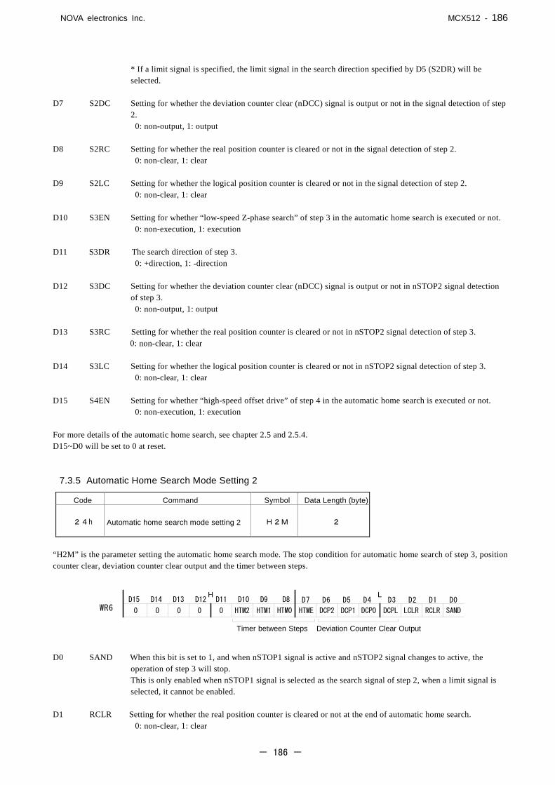
NOVA electronics Inc. MCX512 - 186
- 186 -
* If a limit signal is specified, the limit signal in the search direction specified by D5 (S2DR) will be selected.
D7 S2DC Setting for whether the deviation counter clear (nDCC) signal is output or not in the signal detection of step
2. 0: non-output, 1: output
D8 S2RC Setting for whether the real position counter is cleared or not in the signal detection of step 2.
0: non-clear, 1: clear D9 S2LC Setting for whether the logical position counter is cleared or not in the signal detection of step 2.
0: non-clear, 1: clear D10 S3EN Setting for whether “low-speed Z-phase search” of step 3 in the automatic home search is executed or not.
0: non-execution, 1: execution D11 S3DR The search direction of step 3.
0: +direction, 1: -direction D12 S3DC Setting for whether the deviation counter clear (nDCC) signal is output or not in nSTOP2 signal detection
of step 3. 0: non-output, 1: output
D13 S3RC Setting for whether the real position counter is cleared or not in nSTOP2 signal detection of step 3.
0: non-clear, 1: clear D14 S3LC Setting for whether the logical position counter is cleared or not in nSTOP2 signal detection of step 3.
0: non-clear, 1: clear D15 S4EN Setting for whether “high-speed offset drive” of step 4 in the automatic home search is executed or not.
0: non-execution, 1: execution For more details of the automatic home search, see chapter 2.5 and 2.5.4. D15~D0 will be set to 0 at reset.
7.3.5 Automatic Home Search Mode Setting 2
Code Command Symbol Data Length (byte)
24h Automatic home search mode setting 2 H2M 2
“H2M” is the parameter setting the automatic home search mode. The stop condition for automatic home search of step 3, position counter clear, deviation counter clear output and the timer between steps.
D0 SAND When this bit is set to 1, and when nSTOP1 signal is active and nSTOP2 signal changes to active, the
operation of step 3 will stop. This is only enabled when nSTOP1 signal is selected as the search signal of step 2, when a limit signal is selected, it cannot be enabled.
D1 RCLR Setting for whether the real position counter is cleared or not at the end of automatic home search.
0: non-clear, 1: clear
D7 D6 D5 D4H L
D15 D14 D13 D12 D11 D10 D9 D8 D3 D2 D1 D0WR6 HTM0HTM1HTM2 HTME DCP0DCP1DCP2 DCPL RCLRLCLR SAND0 0000
Deviation Counter Clear OutputTimer between Steps

NOVA electronics Inc. MCX512 - 187
- 187 -
D2 LCLR Setting for whether the logical position counter is cleared or not at the end of automatic home search.
0: non-clear, 1: clear D3 DCPL Setting the logical level of deviation counter clear (nDCC) output pulses.
0: positive logical pulse, 1: negative logical pulse
D6~4 DCP2~0 Setting the output pulse width of deviation counter clear (nDCC).
(When CLK=16MHz) D6~4
(DCP2~0) Output Pulse Width
0 10μsec 1 20μsec 2 100μsec 3 200μsec 4 1msec 5 2msec 6 10msec 7 20msec
D7 HTME Enables the timer between steps.
0: disable, 1: enable D10~8 HTM2~0 Specifies the interval of the timer between steps.
(When CLK=16MHz) D10~8 (HTM2~0)
Timer Time
0 1 msec 1 2msec 2 10msec 3 20msec 4 100msec 5 200msec 6 500msec 7 1000msec
For more details of the automatic home search, see chapter 2.5 and 2.5.4. D15~D0 will be set to 0 at reset. D15~D11 should always be set to 0.
Positive Logical Pulse: Negative Logical Pulse:
Output Pulse Width
(Positive Logical Pulse)

NOVA electronics Inc. MCX512 - 188
- 188 -
7.3.6 Input Signal Filter Mode Setting
Code Command Symbol Data Length (byte)
25h Input signal filter mode setting FLM 2
“FLM” is the parameter setting the enable/disable of input signal filter and the time constant of 2 filters.
D7~0 FE7~0 For each input signals as shown in the table below, it can set whether the IC built-in filter function is
enabled or the signal is passed through. 0: disable (through), 1: enable
Specified bit Input signal Applied time constant
D0(FE0) EMGN D1(FE1) nLMTP, nLMTM D2(FE2) nSTOP0, nSTOP1
Filter Time Constant A D3(FE3) nINPOS, nALARM D4(FE4) nPIO7~0 D5(FE5) nPIO13~8 D6(FE6) nSTOP2
Filter Time Constant B D7(FE7) nECA, nECB
D11~8 FL03~00 Set the time constant of the input signal filter specified by D5~D0 (FE5~0) to Filter Time Constant A. D15~12 FL13~10 Set the time constant of the input signal filter specified by D7, D6 (FE7, 6) to Filter Time Constant B.
(When CLK=16MHz) Time Constant
(Hex) Removable maximum
noise width Input signal delay time
0 437.5nsec 500nsec 1 875nsec 1ec.5 2 1.75μ.75 2.75μ 3 3.5μ.5e 4secc 4 7μμse 8secc 5 14μ4se 16eccs 6 28μ8μs 32ecec 7 56μ6μs 64ecec 8 112sece 128μsec 9 224μ24μ 256μsec A 448μ48μ 512μsec B 896μ96μ 1.024msec C 1.792msec 2.048msec D 3.584msec 4.096msec E 7.168msec 8.192msec F 14.336msec 16.384msec
See chapter 2.11 for details of input signal filter function. D15~D0 will be set as 0 at reset.
D7 D6 D5 D4H L
D15 D14 D13 D12 D11 D10 D9 D8 D3 D2 D1 D0WR6 FL00FL01FL02 FE7 FE4FE5FE6 FE3 FE1FE2 FE0FL13 FL03FL10FL11FL12
Filter Time Constant B Enable / disable of Input Signal FilterFilter Time Constant A
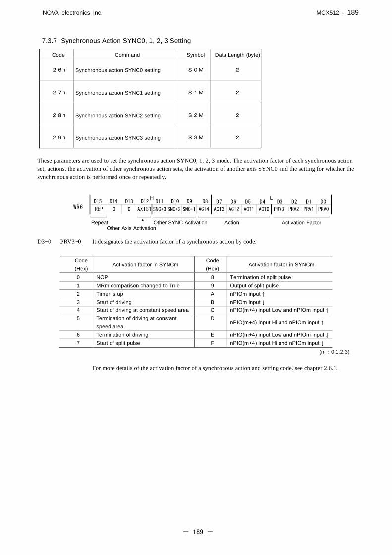
NOVA electronics Inc. MCX512 - 189
- 189 -
7.3.7 Synchronous Action SYNC0, 1, 2, 3 Setting
Code Command Symbol Data Length (byte)
26h Synchronous action SYNC0 setting S0M 2
27h Synchronous action SYNC1 setting S1M 2
28h Synchronous action SYNC2 setting S2M 2
29h Synchronous action SYNC3 setting S3M 2
These parameters are used to set the synchronous action SYNC0, 1, 2, 3 mode. The activation factor of each synchronous action set, actions, the activation of other synchronous action sets, the activation of another axis SYNC0 and the setting for whether the synchronous action is performed once or repeatedly.
D3~0 PRV3~0 It designates the activation factor of a synchronous action by code.
(m:0,1,2,3)
For more details of the activation factor of a synchronous action and setting code, see chapter 2.6.1.
AXIS1WR6D7 D6 D5 D4
H LD15 D14 D13 D12 D11 D10 D9 D8 D3 D2 D1 D0
PRV0PRV1PRV2PRV3ACT0ACT1ACT2ACT4 ACT3SNC+1SNC+2SNC+3REP 00
Activation FactorActionRepeat Other SYNC ActivationOther Axis Activation
Code (Hex)
Activation factor in SYNCm Code (Hex)
Activation factor in SYNCm
0 NOP 8 Termination of split pulse 1 MRm comparison changed to True 9 Output of split pulse 2 Timer is up A nPIOm input ↑ 3 Start of driving B nPIOm input ↓ 4 Start of driving at constant speed area C nPIO(m+4) input Low and nPIOm input ↑ 5 Termination of driving at constant
speed area D
nPIO(m+4) input Hi and nPIOm input ↑
6 Termination of driving E nPIO(m+4) input Low and nPIOm input ↓ 7 Start of split pulse F nPIO(m+4) input Hi and nPIOm input ↓

NOVA electronics Inc. MCX512 - 190
- 190 -
D84 ACT40 It designates the action of a synchronous action by code.
(m:0,1,2,3)
DV:Drive speed TP:Drive pulse number/Finish point
SP1:Split pulse setting 1
LP:Logical position counter RP:Real position counter SV:Initial speed
AC:Acceleration CT:Current timer value CV:Current drive speed
CA:Current acceleration/deceleration
For more details of the action of synchronous action and setting code, see chapter 2.6.2. D11~9 SNC+3~1 It designates the other synchronous action sets activated by a synchronous action.
0: disable, 1: enable
Self- synchronous action set
D11(SNC+3) D10(SNC+2) D9(SNC+1)
SYNC0 SYNC3 activation SYNC2 activation SYNC1 activation SYNC1 SYNC0 activation SYNC3 activation SYNC2 activation SYNC2 SYNC1 activation SYNC0 activation SYNC3 activation SYNC3 SYNC2 activation SYNC1 activation SYNC0 activation
D12 AXIS1 It designates another axis SYNC0 activated by a synchronous action.
0: disable, 1: enable D15 REP Setting for whether the enable state of synchronous action set is disabled or not once the synchronous action
is activated. 0: disable (once), 1: non-disable (repeat) When this bit is set to 0, and when the activation factor becomes active, the synchronous action is activated only the first time. When this bit is set to 1, the synchronous action is activated whenever the activation factor becomes active.
To re-enable the synchronous action that is disabled, write a synchronous action enable command. Enable/disable setting of synchronous action SYNC3~0 can be checked by RR0 register.
For more details of the synchronous action, see chapter 2.6. D15~D0 will be set to 0 at reset.
Code (Hex)
Action in SYNCm Code (Hex)
Action in SYNCm
00 NOP 0C Start of absolute position driving 01 Load MRm → DV 0D Start of +direction continuous pulse driving 02 Load MRm → TP 0E Start of -direction continuous pulse driving 03
Load MRm → SP1 0F Relative position driving by drive pulse
number of MRm value
04 Load MRm → LP(SYNC0),RP(SYNC1),
10 Absolute position driving to the finish point of MRm value
SV(SYNC2),AC(SYNC3) 11 Decelerating stop 05 Save LP → MRm 12 Instant stop 06 Save RP → MRm 13 Drive speed increase 07 Save CT → MRm 14 Drive speed decrease 08 Save CV(SYNC0),CA(SYNC1) → MRm 15 Timer-start 09 Synchronous pulse nPIOm output 16 Timer-stop 0A Start of relative position driving 17 Start of split pulse 0B Start of counter relative position driving 18 Termination of split pulse
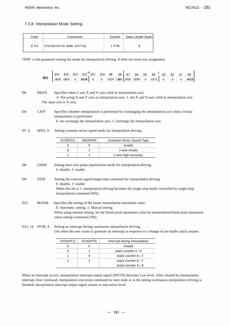
NOVA electronics Inc. MCX512 - 191
- 191 -
7.3.8 Interpolation Mode Setting
Code Command Symbol Data Length (byte)
2Ah Interpolation mode setting IPM 2
“IPM” is the parameter setting the mode for interpolation driving. It does not need axis assignment.
D0 HKEN Specifies when it sets X and Y-axis valid as interpolation axis.
0: Not using X and Y-axis as interpolation axis. 1: Set X and Y-axis valid as interpolation axis The main axis is X-axis.
D4 CXIV Specifies whether interpolation is performed by exchanging the interpolation axis when circular
interpolation is performed. 0: not exchange the interpolation axis, 1: exchange the interpolation axis D7, 6 SPD1, 0 Setting constant vector speed mode for interpolation driving.
D7(SPD1) D6(SPD0) Constant Vector Speed Type
0 0 invalid 0 1 2-axis simple 1 1 2-axis high-accuracy
D8 LMDF Setting short axis pulse equalization mode for interpolation driving. 0: disable, 1: enable D9 STEP Setting the external signal/single-step command for interpolation driving. 0: disable, 1: enable When this bit is 1, interpolation driving becomes the single-step mode controlled by single-step
interpolation command (6Fh). D12 MAXM Specifies the setting of the linear interpolation maximum value. 0: Automatic setting, 1: Manual setting
When using manual setting, set the finish point maximum value by interpolation/finish point maximum value setting command (19h).
D15, 14 INTB, A Setting an interrupt during continuous interpolation driving. Use when the user wants to generate an interrupt in response to a change of pre-buffer stack counter.
D15(INT1) D14(INT0) Interrupt during Interpolation 0 0 Invalid 0 1 stack counter 4→3 1 0 stack counter 8→7 1 1 stack counter 8→7
stack counter 4→3 When an interrupt occurs, interpolation interrupt output signal (INT1N) becomes Low level. After cleared by interpolation interrupt clear command, interpolation execution command for next node or at the timing continuous interpolation driving is finished, interpolation interrupt output signal returns to non-active level.
HKEN
D7 D6 D5 D4H L
D15 D14 D13 D12 D11 D10 D9 D8 D3 D2 D1 D0WR6 000CXIV0SPD0SPD1LMDFSTEP00MAXM0INTAINTB

NOVA electronics Inc. MCX512 - 192
- 192 -
[Note]
• When terminating interpolation driving, write 0 into WR6 register and write this mode setting command, then be sure to clear interpolation mode. Otherwise, driving will not work properly.
D15~D0 will be set to 0 at reset. D1~3, 5, 10, 11, 13 should always be set to 0. 7.3.9 PIO Signal Setting 3
Code Command Symbol Data Length (byte)
2Bh PIO signal setting 3 P3M 2
“P3M” is the parameter setting the function of nPIO13~8 signals. nPIO13~8 signals can be used as general input/output signal.
D5~0 PnM Setting nPIOm (m:13~8) signal function. 0: Using as general input signal 1: Using as general output signal
When using as general input, nPIO13~8 signals become input status. For the signal level, X-axis can be read by D13~8 of RR4 register, Y-axis can be read by D13~8 of RR5 register. When using as general output, nPIO13~8 signals become output status. D13~8 of WR4 register is output to PIO13~8 of X-axis, D13~8 of WR5 register is output to PIO13~8 of Y-axis,
For more details of using nPIO13~8 signals, see chapter 2.8.
D15~D0 will be set as 0 at reset. D5~6 should always be set as 0.
W R 6
H L D15 D14 D13 D12 D11 D10 D9 D8 D7 D6 D5 D4 D3 D2 D1 D0
P 1 0 M P 9 M P 1 2 M 0 P 8 M P 1 1 M P 1 3 M 0
nPIO13~8 signal
0 0 0 0 0 0 0 0

NOVA electronics Inc. MCX512 - 193
- 193 -
7.4 Commands for Reading Data
Commands for reading data are used to read the internal register. After a data reading command is written into register WR0, this data will be set to registers RR6 and RR7. The user can obtain a specified data by reading the registers RR6 and RR7. When the data length is 2 bytes, the data will be set to register RR6 and when it is 4 bytes, the data will be set to registers RR6 and RR7. Reading data is binary and 2's complement is used for negative numbers. [Note]
• It requires 125 nSEC (maximum) to access the command code of data reading when CLK = 16MHz. After the command is written and passed that time, read registers RR6 and 7.
• The unit described in each speed parameter and timer value is for when input clock (CLK) is 16MHz. Please see Appendix B for parameter calculation formula when input clock (CLK) is other than 16MHz.
• The axis assignment should be only 1 axis.
7.4.1 Logical Position Counter Reading
Code Command Symbol Data Range Data Length (byte)
30h Logical position counter reading LP -2,147,483,648 ~ +2,147,483,647 4
The current value of logical position counter is set to read registers RR6 and RR7.
7.4.2 Real Position Counter Reading
Code Command Symbol Data Range Data Length (byte)
31h Real position counter reading RP -2,147,483,648 ~ +2,147,483,647 4
The current value of real position counter is set to read registers RR6 and RR7.
7.4.3 Current Drive Speed Reading
Code Command Symbol Data Range Data Length (byte)
32h Current drive speed reading CV 0 ~ 8,000,000 4
The value of current drive speed is set to read registers RR6 and RR7. When the driving stops, the value becomes 0. The unit of the setting value is pps which is the same as Drive speed setting (DV). During interpolation driving, calculated pulse speed of the main axis can be read, other axes cannot be read.

NOVA electronics Inc. MCX512 - 194
- 194 -
7.4.4 Current Acceleration/Deceleration Reading
Code Command Symbol Data Range Data Length (byte)
33h Current acceleration/deceleration
reading CA 0 ~ 536,870,911 4
In acceleration/deceleration driving, the value of current acceleration speed during acceleration and current deceleration speed during deceleration is set to read registers RR6 and RR7. While driving stops, 0 will be read out. The unit of the setting value is pps/sec which is the same as Acceleration setting (AC) and Deceleration setting (DC). [Note]
• At constant speed area in linear acceleration/deceleration driving (symmetrical), the acceleration setting value will always be read out during the driving.
• At constant speed area in S-curve acceleration/deceleration driving, the read value will be invalid.
7.4.5 Multi-Purpose Register 0 Reading
Code Command Symbol Data Range Data Length (byte)
34h Multi-purpose register 0 reading MR0 -2,147,483,648 ~ +2,147,483,647 4
The value of multi-purpose register MR0 is set to read registers RR6 and RR7. It can be used to read out the current position, timer value and speed value saved to MR0 by a synchronous action.
7.4.6 Multi-Purpose Register 1 Reading
Code Command Symbol Data Range Data Length (byte)
35h Multi-purpose register 1 reading MR1 -2,147,483,648 ~ +2,147,483,647 4
The value of multi-purpose register MR1 is set to read registers RR6 and RR7. It can be used to read out the current position, current timer value and current acceleration/deceleration value saved to MR1 by a synchronous action.
7.4.7 Multi-Purpose Register 2 Reading
Code Command Symbol Data Range Data Length (byte)
36h Multi-purpose register 2 reading MR2 -2,147,483,648 ~ +2,147,483,647 4
The value of multi-purpose register MR2 is set to read registers RR6 and RR7. It can be used to read out the current position and timer value saved to MR2 by a synchronous action.

NOVA electronics Inc. MCX512 - 195
- 195 -
7.4.8 Multi-Purpose Register 3 Reading
Code Command Symbol Data Range Data Length (byte)
37h Multi-purpose register 3 reading MR3 -2,147,483,648 ~ +2,147,483,647 4
The value of multi-purpose register MR3 is set to read registers RR6 and RR7. It can be used to read out the current position and timer value saved to MR3 by a synchronous action.
7.4.9 Current Timer Value Reading
Code Command Symbol Data Range Data Length (byte)
38h Current timer value reading CT 0 ~ 2,147,483,647 4
The value of current timer value in operation is set to read registers RR6 and RR7. While timer stops, 0 will be read out. The unit of the setting value is µsec which is the same as Timer value setting (TM)
7.4.10 Interpolation/Finish point maximum value Reading
Code Command Symbol Data Range Data Length (byte)
39h Interpolation/Finish point maximum
value reading TX 1~2,147,483,646 4
The maximum value of the finish point of each axis in linear interpolation is set to read registers RR6 and RR7. The axis assignment is not necessary for this command. The read values differ before and during interpolation driving. Before interpolation driving, the finish point maximum value at the interpolation segment being inputted will be read. During interpolation driving, the finish point maximum value at the interpolation segment currently being executed will be read.
7.4.11 WR1 Setting Value Reading
Code Command Symbol Data Range Data Length (byte)
3Dh WR1 setting value reading WR1 (Bit data) 2
The setting value of WR1 register is set to read register RR6. WR1 setting value cannot be read by accessing WR1 register address. To check and read out the WR1 setting value, use this command. Read register RR7 is set to 0.

NOVA electronics Inc. MCX512 - 196
- 196 -
7.4.12 WR2 Setting Value Reading
Code Command Symbol Data Range Data Length (byte)
3Eh WR2 setting value reading WR2 (Bit data) 2
The setting value of WR2 register is set to read register RR6. WR2 setting value cannot be read by accessing WR2 register address. To check and read out the WR2 setting value, use this command. Read register RR7 is set as 0.
7.4.13 WR3 Setting Value Reading
Code Command Symbol Data Range Data Length (byte)
3Fh WR3 setting value reading WR3 (Bit data) 2
The setting value of WR3 register is set to read register RR6. WR3 setting value cannot be read by accessing WR3 register address. To check and read out the WR3 setting value, use this command. Read register RR7 is set as 0.
7.4.14 Multi-Purpose Register Mode Setting Reading
Code Command Symbol Data Range Data Length (byte)
40h Multi-purpose register mode setting
reading MRM (Bit data) 2
The value set by multi-purpose register mode setting command (20h) is set to read register RR6. Read register RR7 is set as 0.
7.4.15 PIO Signal Setting 1 Reading
Code Command Symbol Data Range Data Length (byte)
41h PIO signal setting 1 reading P1M (Bit data) 2
The value set by PIO signal setting 1 command (21h) is set to read register RR6. Read register RR7 is set as 0.

NOVA electronics Inc. MCX512 - 197
- 197 -
7.4.16 PIO Signal Setting 2/Other Settings Reading
Code Command Symbol Data Range Data Length (byte)
42h PIO signal setting 2/Other settings
reading P2M (Bit data) 2
The value set by PIO signal setting 2/other settings command (22h) is set to read register RR6. Read register RR7 is set as 0.
7.4.17 Acceleration Setting Value Reading
Code Command Symbol Data Range Data Length (byte)
43h Acceleration setting value reading AC 1 ~ 536,870,911 4
The value set by acceleration setting command (02h) is set to read registers RR6 and RR7. The unit of the setting value is pps/sec. When MR3 value is loaded to acceleration setting value (AC) by a synchronous action, that value will be read out.
7.4.18 Initial Speed Setting Value Reading
Code Command Symbol Data Range Data Length (byte)
44h Initial speed setting value reading SV 1 ~ 8,000,000 4
The value set by initial speed setting command (04h) is set to read registers RR6 and RR7. The unit of the setting value is pps. When MR2 value is loaded to initial speed setting value (SV) by a synchronous action that value will be read out.
7.4.19 Drive Speed Setting Value Reading
Code Command Symbol Data Range Data Length (byte)
45h Drive speed setting value reading DV 1 ~ 8,000,000 4
The value set by drive speed setting command (05h) is set to read registers RR6 and RR7. The unit of the setting value is pps. When MRm value is loaded to drive speed setting value (DV) by a synchronous action, that value will be read out.
NOVA electronics Inc. MCX512 - 198
- 198 -
7.4.20 Drive Pulse Number/Finish Point Setting Value Reading
Code Command Symbol Data Range Data Length (byte)
46h Drive pulse number/Finish point setting
value reading TP -2,147,483,646 ~ +2,147,483,646 4
The value set by drive pulse number/finish point setting command (06h) is set to read registers RR6 and RR7. When MRm value is loaded to drive pulse number/finish point setting value (TP) by a synchronous action, that value will be read out.
7.4.21 Split Pulse Setting 1 Reading
Code Command Symbol Data Range Data Length (byte)
47h Split pulse setting 1 reading SP1 RR6 Split length:2 ~ 65,535
4 RR7 Pulse width:1 ~ 65,534
The value set by Split pulse setting 1 command (17h) is set to read registers RR6 and RR7. The split length is set to RR6 and the pulse width is set into RR7. When MRm value is loaded to split pulse setting 1 (SP1) by a synchronous action, that value will be read out.
7.4.22 General Purpose Input Value Reading
Code Command Symbol Data Range Data Length (byte)
48h General purpose input value reading UI RR6: 2 bytes (D15~0 in I2C
communication) 2
The axis assignment is not necessary for this command. In I2C serial interface bus mode, the signal levels of D15~0 (pin number 1~8, 11~18) are set to read register RR6.
7.4.23 PIO Signal Setting 3
Code Command Symbol Data Range Data Length (byte)
42h PIO signal setting 3 P3M (Bit data) 2
The value set by PIO signal setting 3 is set to read register RR6. Read register RR7 is set as 0.
D7 D6 D5 D4H L
D15 D14 D13 D12 D11 D10 D9 D8 D3 D2 D1 D0RR6
D7 D6 D5 D4D15 D14 D13 D12 D11 D10 D9 D8 D3 D2 D1 D0
NOVA electronics Inc. MCX512 - 199
- 199 -
7.5 Driving Commands
Driving commands include the commands for drive pulse output for each axis and other related commands. After the command code is written with axis assignment in command register WR0, the command will be executed immediately. In driving, the n-DRV bit of main status register RR0 becomes 1. When the driving is finished, n-DRV bit will return to 0. If nINPOS input signal for a servo driver is enabled, the n-DRV bit of main status register RR0 will not return to 0 until nINPOS signal is on its active level after the driving is finished. [Note]
• It requires 125 nSEC (maximum) to access the command code when CLK = 16MHz. Please write the next command after this period of time.
7.5.1 Relative Position Driving
Code Command
50h Relative position driving
The signed drive pulse number that is set will be output from the +direction drive pulse signal (nPP) or the -direction drive pulse signal (nPM). When the drive pulse number is positive, it will be output from the output signal nPP, and when it is negative, it will be output from the output signal nPM. (When the pulse output type is independent 2-pulse) In driving, when one pulse of +direction drive pulses is output, the logical position counter will count up 1, and when one pulse of -direction drive pulses is output, the logical position counter will count down 1. Before writing the driving command, the user should set the parameters for the outputting speed curve and the drive pulse number appropriately (see the table below).
:Required
Parameter
Speed curve to be output Fixed speed Symmetrical linear
acceleration/ deceleration
Non-symmetrical linear acceleration
/deceleration
Symmetrical S-curve acceleration
/deceleration
Non-symmetrical S-curve acceleration
/deceleration Jerk (JK)
Deceleration increasing rate (DJ)
Acceleration (AC) * * Deceleration (DC) * Initial speed (SV) Drive speed (DV)
Drive pulse number/Finish point (TP)
Manual deceleration point (DP)
*Note: Set the maximum value of 536,870,911 (1FFF FFFFh). However, in Partial S-curve acceleration/deceleration driving, set the acceleration/deceleration at the linear acceleration/deceleration part.

NOVA electronics Inc. MCX512 - 200
- 200 -
7.5.2 Counter Relative Position Driving
Code Command
51h Counter relative position driving
The signed drive pulse number that is set will be output from the +direction drive pulse signal (nPP) or the -direction drive pulse signal (nPM). When the drive pulse number is positive, it will be output from the output signal nPM, and when it is negative, it will be output from the output signal nPP. (When the pulse output type is independent 2-pulse) This command can be used to output the predetermined drive pulse number in the different direction by driving commands. Usually, set the positive pulses to the drive pulse number (TP). When the user needs to drive in the +direction, write relative position driving command (50h) and when to drive in the -direction, write counter relative position driving command (51h). In driving, when one pulse of +direction drive pulses is output, the logical position counter will count up 1, and when one pulse of -direction drive pulses is output, the logical position counter will count down 1. Before writing the driving command, the user should set the parameters for the outputting speed curve and the drive pulse number appropriately.
7.5.3 + Direction Continuous Pulse Driving
Code Command
52h + Direction continuous pulse driving
Until the stop command or specified external signal becomes active, pulse numbers will be output through the output signal nPP continuously. (When the pulse output type is independent 2-pulse) In driving, when one pulse of drive pulses is output, the logical position counter will count up 1. Before writing the driving command, the user should set the parameters for the outputting speed curve appropriately.
7.5.4 − Direction Continuous Pulse Driving
Code Command
53h − Direction continuous pulse driving
Until the stop command or specified external signal becomes active, pulse numbers will be output through the output signal nPM continuously. (When the pulse output type is independent 2-pulse) In driving, when one pulse of drive pulses is output, the logical position counter will count down 1. Before writing the driving command, the user should set the parameters for the outputting speed curve appropriately.

NOVA electronics Inc. MCX512 - 201
- 201 -
7.5.5 Absolute Position Driving
Code Command
54h Absolute position driving
This command performs the driving from present point to finish point. Before driving, the destination point based on a home (logical position counter = 0) should be set with a signed 32-bit value by drive pulse number/finish point setting command (06h). Before writing the driving command, the user should set the parameters for the outputting speed curve and finish point appropriately.
7.5.6 Decelerating Stop
Code Command
56h Decelerating stop
This command performs the decelerating stop when the drive pulses are outputting. If the speed is lower than the initial speed during the driving, the driving will stop instantly. During interpolation driving, when decelerating stop or instant stop command is written to the main axis, interpolation driving stops. Once the driving stops, this command will not work.
7.5.7 Instant Stop
Code Command
57h Instant stop
This command performs the instant stop when the drive pulses are outputting. Also, the instant stop can be performed in acceleration/deceleration driving. Once the driving stops, this command will not work.
7.5.8 Direction Signal + Setting
Code Command
58h Direction signal + setting
This command is used to set the direction signal DIR to the active level of the +direction before driving when the pulse output type is 1-pulse 1-direction. As shown in 11.2, once the driving is started in the 1-pulse 1-direction type, the first pulse of drive pulses will be output after 1CLK from when the direction signal is determined. This command can be used to determine the direction signal in the +direction when the user needs to take longer time than time to set up the direction signal for drive pulses.

NOVA electronics Inc. MCX512 - 202
- 202 -
7.5.9 Direction Signal - Setting
Code Command
59h Direction signal − setting
This command is used to set the direction signal DIR to the active level of the -direction before driving when the pulse output type is 1-pulse 1-direction. As shown in 11.2, once the driving is started in the 1-pulse 1-direction type, the first pulse of drive pulses will be output after 1CLK from when the direction signal is determined. This command can be used to determine the direction signal in the -direction when the user needs to take longer time than time to set up the direction signal for drive pulses.
7.5.10 Automatic Home Search Execution
Code Command
5Ah Automatic home search execution
This command executes automatic home search. Before execution of the command, the automatic home search mode and correct parameters must be set. See chapter 2.5 for details of automatic home search.

NOVA electronics Inc. MCX512 - 203
- 203 -
7.6 Interpolation Commands
Interpolation commands consist of the commands for 2axes linear interpolation, CW/CCW circular interpolation, 2axes bit pattern interpolation, and other related commands. The axis assignment to D11~8 bits of command register WR0 is not necessary for interpolation commands, set 0 to those bits. Before the interpolation command is executed, be sure to check the following: a. interpolation axes valid setting (set in interpolation mode setting)
b. speed parameter setting for main axis, X-axis In interpolation driving, n-DRV bit of interpolating axis in main status register RR0 becomes 1, and will return to 0 when the driving is finished. [Note]
• It requires 125nSEC (maximum) to access the command code when CLK=16MHz. Please write the next command after this period of time.
7.6.1 2-axis Linear Interpolation Driving
Code Command
61h 2-axis linear interpolation driving
This command performs 2-axis interpolation from present point to finish point. Before driving, the finish point of the 2 corresponding axes should be set by incremental value.
7.6.2 CW Circular Interpolation Driving
Code Command
64h CW circular interpolation driving
This command performs 2-axis clockwise circular interpolation based on center point, from present point to finish point.
Before driving, the finish t and the center point of the 2 corresponding axes should be set by incremental value.
A full circle will come out if the finish position is set (0, 0).
7.6.3 CCW Circular Interpolation Driving
Code Command
65h CCW circular interpolation driving
This command performs 2-axis counterclockwise circular interpolation based on center point, from present point to finish point.
Before driving, the finish and center point of the 2 corresponding axes should be set by incremental value.
A full circle will come out If the finish position is set (0, 0).

NOVA electronics Inc. MCX512 - 204
- 204 -
7.6.4 2-Axis Bit Pattern Interpolation Driving
Code Command
66h 2-axis bit pattern interpolation driving
This command performs 2-axis bit pattern interpolation. Before driving, the +/- direction bit data of the two interpolating axes should be set, and the setting bit data of each axis (each direction) is at most 16 × 8 = 128-bit. Once the data is over 128-bit, those remaining data can be filled during the driving.
7.6.5 Deceleration Enabling
Code Command
6Dh Deceleration enabling
This command enables the automatic or manual deceleration in interpolation. In individual interpolation, the user must write this command before the driving. However, in continuous interpolation, this command should be put in before writing the interpolation command of the interpolation node to be decelerated. The deceleration is disabled while resetting. When the deceleration enabling command is written, the enabling status is kept until interpolation driving is finished, the deceleration disabling command (6Eh) is written or the reset is performed. Deceleration enabling/disabling only works during interpolation driving. When driving each axis individually, automatic and manual deceleration is always enabled.
7.6.6 Deceleration Disabling
Code Command
6Eh Deceleration disabling
This command disables the automatic or manual deceleration in interpolation.
7.6.7 Interpolation Interrupt Clear/Single-step Interpolation
Code Command
6Fh Interpolation interrupt clear/Single-step interpolation
Interpolation interrupt clear command clears the interrupt (INT1N) generated in continuous interpolation. Single-step interpolation command performs 1-pulse (each step) output in interpolation driving. For details of interrupt, see chapter 2.10 and for details of single-step interpolation, see chapter 3.9.

NOVA electronics Inc. MCX512 - 205
- 205 -
7.7 Synchronous Action Operation Commands
Synchronous action operation commands are used to enable, disable or activate a synchronous action. There are 4 synchronous action sets: SYNC0, 1, 2, 3 and any of synchronous action sets can be enabled, disabled or activated at the same time. For synchronous action operation commands, set the operation command code to the four D7~D4 bits of WR0 command register and set the synchronous action set which the user wants to operate to the four D3~D0 bits of WR0. That is, when the user wants to enable the synchronous action, set 8h to D7~D4, and when to disable it, set 9h to D7~D4, and when to activate it, set Ah to D7~D4. D3~D0 are corresponding to four synchronous action sets: SYNC3, SYNC2, SYNC1, SYNC0, and set 1 to the bit corresponding to the synchronous action set.
These commands are without writing data and executed by writing the axis assignment and command code into WR0 command register. [Note]
• It requires 125 nSEC (maximum) to access the command code of synchronous action operation commands when CLK=16MHz. Please write the next command after this period of time.
7.7.1 Synchronous Action Enable Setting
Code Command
81h
~8Fh Synchronous action enable setting
This command sets to enable each synchronous action set which is specified by the lower 4-bit of the command code. Before the synchronous action enable setting, the mode setting for the synchronous action set which the user wants to enable must be set by synchronous action SYNC3~0 setting command (29h~26h). Example:To enable the synchronous action sets SYNC0 and SYNC2 in X-axis, write 0185h into WR0. The enable/disable state of synchronous action SYNC3~0 can be checked by Page 1 of RR3 register. When resetting, all of SYNC3~0 will be disabled. [Note]
• By using PIO signal setting 2/other settings command (22h), when the synchronous action activated by an error is disabled by the setting (D7:ERRDE bit = 1) and when an error occurs (n-ERR bit of RR0 register is 1.), this command cannot be set to enable the synchronous action. Write the synchronous action enable setting command after clearing n-ERR bit by such as error/finishing status clear command (79h).
D7 D6 D5 D4H L
D15 D14 D13 D12 D11 D10 D9 D8 D3 D2 D1 D0WR0 0 000
Synchronous actionoperation command code
SYNC0SYNC1SYNC2SYNC3
Designation of SYNC3~0
8h:Enable, 9h:Disable, Ah:Activation1:Set
Axis Assignment
00

NOVA electronics Inc. MCX512 - 206
- 206 -
7.7.2 Synchronous Action Disable Setting
Code Command
91h
~9Fh Synchronous action disable setting
This command sets to disable each synchronous action set which is specified by the lower 4-bit of the command code. Once the synchronous action is set to disable, it cannot be activated by an activation factor or synchronous action activation command. Example:To disable the synchronous action sets SYNC1 and SYNC3 in X-axis, write 019Ah into WR0. The enable/disable state of synchronous action SYNC3~0 can be checked by Page 1 of RR3 register. When resetting, all of SYNC3~0 will be disabled.
7.7.3 Synchronous Action Activation
Code Command
A1h
~AFh Synchronous action activation
This command sets to activate each synchronous action set which is specified by the lower 4-bit of the command code. Before the synchronous action is activated, the mode setting for the synchronous action set which the user wants to activate must be set by synchronous action SYNC3~0 setting command (29h~26h). And the synchronous action set which the user wants to activate must be enabled by synchronous action enable setting command. The enable/disable state of synchronous action SYNC3~0 can be checked by Page 1 of RR3 register. Example:To activate the synchronous action set SYNC0 in X-axis, write 01A1h into WR0. To activate all the synchronous action sets SYNC3~0 in X-axis, write 01AFh into WR0.

NOVA electronics Inc. MCX512 - 207
- 207 -
7.8 Other Commands
These commands are without writing data and executed by writing the axis assignment and command code into WR0 command register. [Note]
• It requires 125 nSEC (maximum) to access the command code when CLK=16MHz. Please write the next command after this period of time.
7.8.1 Speed Increase
Code Command
70h Speed increase
This command increases a speed by the value of the speed increasing/decreasing value setting during the driving. The speed increasing/decreasing value (IV) must be set by speed increasing/decreasing value setting command (15h) in advance. This command can be used during continuous pulse driving and cannot be used during fixed pulse driving. If this command is used frequently during fixed pulse driving, premature termination or creep may occur at the termination of driving. In S-curve acceleration/deceleration driving, this command will be invalid even if written during acceleration/deceleration. Make sure to use it during constant speed driving (Page1 of RR3 / D5:CNST=1). The drive speed setting value (DV) is not updated by this command. This command cannot be used in interpolation driving.
7.8.2 Speed Decrease
Code Command
71h Speed decrease
This command decreases a speed by the value of the speed increasing/decreasing value setting during the driving. The speed increasing/decreasing value (IV) must be set by speed increasing/decreasing value setting command (15h) in advance. This command can be used during continuous pulse driving and cannot be used during fixed pulse driving. If this command is used frequently during fixed pulse driving, premature termination or creep may occur at the termination of driving. In S-curve acceleration/deceleration driving, this command will be invalid even if written during acceleration/deceleration. Make sure to use it during constant speed driving (Page1 of RR3/ D5:CNST=1). The drive speed setting value (DV) is not updated by this command. This command cannot be used in interpolation driving.

NOVA electronics Inc. MCX512 - 208
- 208 -
7.8.3 Deviation Counter Clear Output
Code Command
72h Deviation counter clear output
This command outputs deviation counter clear pulses from the nDCC output pin. Before issuing this command, set the logical level of pulses and pulse width by the automatic home search mode setting 2 command (24h). See chapter 2.5.2 and 2.5.4 for details.
7.8.4 Timer-Start
Code Command
73h Timer-start
This command starts a timer. When a timer is started by this command, the current timer value (CT) starts to count up from 0, and when the count reaches the value specified by the timer value (TM), then the timer is up. A timer can be used repeatedly after the time is up. To repeat a timer, set D14 bit (TMMD) of WR3 register to 1. For more details of the timer, see chapter 2.9.
7.8.5 Timer-Stop
Code Command
74h Timer-stop
This command stops a timer. If a timer is stopped before it expires, the current timer value (CT) returns to 0. And if the timer is started again, it counts up from 0.
7.8.6 Start of Split Pulse
Code Command
75h Start of split pulse
This command outputs split pulses. Split pulses are output from the nSPLTP output pin during the driving. SPLIT bit of Page1 of RR3 register which indicates the split pulse is in operation becomes 1 by issuing start of split pulse command. Before issuing this command, each parameter such as a split pulse length must be set appropriately. For more details of each parameter for the split pulse, see chapter 2.7.

NOVA electronics Inc. MCX512 - 209
- 209 -
7.8.7 Termination of Split Pulse
Code Command
76h Termination of split pulse
This command stops to output split pulses. SPLIT bit of Page1 of RR3 register which indicates the split pulse is in operation becomes 0 by issuing termination of split pulse command. When termination of split pulse command is written, if the split pulse output signal is on Hi level, it stops after keeping the Hi level of a specified pulse width. (when the positive logic is set.)
7.8.8 Drive Start Holding
Code Command
77h Drive start holding
This command is to hold-on the start of driving. It can be used for starting multi-axis driving simultaneously. Write this command to the axes that the user wants to start simultaneously, and then write the drive command to each axis. Then, if the drive start holding release command (78h) is written, all axes will start the driving simultaneously. In continuous interpolation driving, this command can be used when interpolation data of necessary segments is set to pre-buffer before the start of driving. For more details of continuous interpolation, see chapter 3.7.
7.8.9 Drive Start Holding Release
Code Command
78h Drive start holding release
This command is to release the drive start holding command (77h), and start the driving.
7.8.10 Error/Finishing Status Clear
Code Command
79h Error/Finishing status clear
All the error information bits and the driving finishing status bits of RR2 register and the error bits (D7~4:n-ERR) of RR0 register are cleared to 0. When the error occurs in interpolation driving, use this command after checking that interpolation drive stops.
NOVA electronics Inc. MCX512 - 210
- 210 -
7.8.11 RR3 Page 0 Display
Code Command
7Ah RR3 Page 0 display
This command displays Page0 of RR3 register. When displaying Page0, D15 bit of RR3 register becomes 0.
7.8.12 RR3 Page 1 Display
Code Command
7Bh RR3 Page 1 display
This command displays Page1 of RR3 register. When displaying Page1, D15 bit of RR3 register becomes 1.
7.8.13 Maximum finish point clear
Code Command
7Ch Maximum finish point clear
In linear interpolation, this command clears the maximum finish point automatically calculated to the interpolation finish point currently written. The axis assignment is not necessary for this command.
7.8.14 NOP
Code Command
1Fh NOP
No operation is performed.

NOVA electronics Inc. MCX512 - 211
- 211 -
7.8.15 Command Reset
Code Command
00FFh Command reset
This command resets the IC. All the upper 8 bits (D15~D8) of WR0 register must be set to 0. The user cannot access the IC for a period of 8CLK (500nsec:CLK=16MHz) after the command code is written. Similarly in 8-bit data bus and I2C serial interface bus, this command must be written to the high word byte (WR0H). The user should write 00h into the high word byte (WR0H), and then write FFh into the low word byte (WR0L). Reset will be executed immediately after writing into the low word byte.

NOVA electronics Inc. MCX512 - 212
- 212 -
8. Connection Examples
8.1 Example of 16-bit Bus Mode Connection
Example of Connection with SH-4CPU and 16-bit Bus Mode
Example of 16-bit Bus Mode Connection
SH-4/SH7760 Examples of Waiting Control Bus Clock 66.664MHz - Setup Waiting 1 cycle insert Resister set:WCR3/A1S0=1 Access Waiting 2 cycles insert Resister set:WCR2/A1W2, A1W1, A1W0 = 010 Hold Waiting 1 cycle insert Resister set:WCR3/A1H1, A1H0 = 01

NOVA electronics Inc. MCX512 - 213
- 213 -
8.2 Example of Connection in I2C Bus Mode
Example of Connection with H8SX1655CPU and I2C Bus Mode
Example of I2C Bus Mode Connection
H8SX1655 Examples of Register Setting Register Address Setting value:8 bit (D7~D0) ICCRA_0 H’FFEB0 10101001 (*)
(*) D7:I2C Bus Interface Enable. Setting 1 enables transfer operation. D5:selectable from master/slave. 1 set to master. D4:selectable from send/receive. 1 is master receive mode and 0 is master send mode (example is 0). D3~D0:select transfer clock. In this case, it is 200kbps (when CLK=16M).
H8SX1655 MCX512
CSN/SCLSCL0(87)
SDA0(86)
+3.3V +3.3V
SDA
3.3k3.3k

NOVA electronics Inc. MCX512 - 214
- 214 -
8.3 Connection Example
The figure below illustrates the connection example of X-axis. All of 2 axes can be configured in the same way as shown below.
8.4 Pulse Output Interface
Output to Motor Driver in Differential Circuit
Open Collector TTL Output
For drive pulse output signals, we recommend the user to use twisted pair shield cable due to the concern of EMC.
+
-
+
-
GND
Twisted Pair Shield Cable
Motor Driver
GND
CW+
CW-
CCW+
CCW-
AM26C32AM26C31
XPP
XPM
MCX512
CW+
CW-
CCW+
CCW-
Twisted Pair Shield Cable
GND
+5V
+5V
74LV06
MCX512
XPP
XPM
Motor Driver

NOVA electronics Inc. MCX512 - 215
- 215 -
8.5 Connection Example for Input Signals
Limit signals often pick up some noise since complicated cabling is normally involved. A photo coupler alone may not be able to absorb this noise. Enable the filter function in the IC and set an appropriate time constant (FL=Ah, Bh).
8.6 Connection Example for Encoder
The following diagram is the example for the encoder signal which is differential line-drive output, then, this signal can be received through the high speed photo coupler IC which can direct it to MCX512.
+3.3V
10K 4.7K
+12~24V
TLP281
MCX512
+Limit
LMTPIntegralFilterEnable
Disable
To the internalcircuit
0.25W
MCX512
220
1K
TLP2066
Motor Driver
ECA+
ECA-
XECA
+3.3V+3.3V
470

NOVA electronics Inc. MCX512 - 216
- 216 -
9. Example Program The example of C program for MCX512 is shown in this chapter. This is a 16-bit bus configuration program. This program can be downloaded from our web site (http://www.novaelec.co.jp/eng/index.html). File name:MCX512Aple.c
#ifndef NULL
#define NULL ((void *)0)
#endif
////////////////////////////////////////////////////////////////////////////////
// Command code definition
////////////////////////////////////////////////////////////////////////////////
//////////////////////////////
// Commands for writing data
//////////////////////////////
#define MCX512_CMD00_JK 0x0000 // Jerk setting
#define MCX512_CMD01_DJ 0x0001 // Deceleration increasing rate setting
#define MCX512_CMD02_AC 0x0002 // Acceleration setting
#define MCX512_CMD03_DC 0x0003 // Deceleration setting
#define MCX512_CMD04_SV 0x0004 // Initial speed setting
#define MCX512_CMD05_DV 0x0005 // Drive speed setting
#define MCX512_CMD06_TP 0x0006 // Drive pulse number/Finish point setting #define MCX512_CMD07_DP 0x0007 // Manual deceleration point setting
#define MCX512_CMD09_LP 0x0009 // Logical position counter setting
#define MCX512_CMD0A_RP 0x000A // Real position counter setting
#define MCX512_CMD0B_SP 0x000B // Software limit + setting
#define MCX512_CMD0C_SM 0x000C // Software limit − setting #define MCX512_CMD0D_AO 0x000D // Acceleration counter offsetting
#define MCX512_CMD0E_LX 0x000E // Logical position counter maximum value
setting
#define MCX512_CMD0F_RX 0x000F // Real position counter maximum value setting
#define MCX512_CMD10_MR0 0x0010 // Multi-purpose register 0 setting
#define MCX512_CMD11_MR1 0x0011 // Multi-purpose register 1 setting
#define MCX512_CMD12_MR2 0x0012 // Multi-purpose register 2 setting
#define MCX512_CMD13_MR3 0x0013 // Multi-purpose register 3 setting
#define MCX512_CMD14_HV 0x0014 // Home search speed setting
#define MCX512_CMD15_IV 0x0015 // Speed increasing/decreasing value setting
#define MCX512_CMD16_TM 0x0016 // Timer value setting
#define MCX512_CMD17_SP1 0x0017 // Split pulse setting 1
#define MCX512_CMD18_SP2 0x0018 // Split pulse setting 2
#define MCX512_CMD19_TX 0x0019 // Interpolation/Finish point maximum value
setting
//////////////////////////////
// Commands for writing mode
//////////////////////////////
#define MCX512_CMD20_MRM 0x0020 // Multi-purpose register mode setting
#define MCX512_CMD21_P1M 0x0021 // PIO signal setting 1
#define MCX512_CMD22_P2M 0x0022 // PIO signal setting 2・Other settings
#define MCX512_CMD23_H1M 0x0023 // Automatic home search mode setting 1
#define MCX512_CMD24_H2M 0x0024 // Automatic home search mode setting 2
#define MCX512_CMD25_FLM 0x0025 // Input signal filter mode setting
#define MCX512_CMD26_S0M 0x0026 // Synchronous action SYNC0 setting
#define MCX512_CMD27_S1M 0x0027 // Synchronous action SYNC1 setting
#define MCX512_CMD28_S2M 0x0028 // Synchronous action SYNC2 setting
#define MCX512_CMD29_S3M 0x0029 // Synchronous action SYNC3 setting
#define MCX512_CMD2A_IPM 0x002A // Interpolation mode setting
#define MCX512_CMD2B_P3M 0x002B // PIO signal setting 3
//////////////////////////////
// Commands for reading data
//////////////////////////////
#define MCX512_CMD30_LP 0x0030 // Logical position counter reading
#define MCX512_CMD31_RP 0x0031 // Real position counter reading
#define MCX512_CMD32_CV 0x0032 // Current drive speed reading
#define MCX512_CMD33_CA 0x0033 // Current acceleration/deceleration reading
#define MCX512_CMD34_MR0 0x0034 // Multi-purpose register 0 reading
#define MCX512_CMD35_MR1 0x0035 // Multi-purpose register 1 reading
NOVA electronics Inc. MCX512 - 217
- 217 -
#define MCX512_CMD36_MR2 0x0036 // Multi-purpose register 2 reading
#define MCX512_CMD37_MR3 0x0037 // Multi-purpose register 3 reading
#define MCX512_CMD38_CT 0x0038 // Current timer value reading
#define MCX512_CMD39_TX 0x0039 // Interpolation/Finish point maximum value
reading
#define MCX512_CMD3D_WR1 0x003D // WR1 setting value reading
#define MCX512_CMD3E_WR2 0x003E // WR2 setting value reading
#define MCX512_CMD3F_WR3 0x003F // WR3 setting value reading
#define MCX512_CMD40_MRM 0x0040 // Multi-purpose register mode setting reading
#define MCX512_CMD41_P1M 0x0041 // PIO signal setting 1 reading
#define MCX512_CMD42_P2M 0x0042 // PIO signal setting 2・Other settings
reading
#define MCX512_CMD43_AC 0x0043 // Acceleration setting value reading
#define MCX512_CMD44_SV 0x0044 // Initial speed setting value reading
#define MCX512_CMD45_DV 0x0045 // Drive speed setting value reading
#define MCX512_CMD46_TP 0x0046 // Drive pulse number/Finish point setting value reading
#define MCX512_CMD47_SP1 0x0047 // Split pulse setting 1 reading
#define MCX512_CMD48_UI 0x0048 // General purpose input value
reading
#define MCX512_CMD49_P3M 0x0049 // PIO signal setting 3 reading
//////////////////////////////
// Driving commands
//////////////////////////////
#define MCX512_CMD50_DRVRL 0x0050 // Relative position driving
#define MCX512_CMD51_DRVNR 0x0051 // Counter relative position driving
#define MCX512_CMD52_DRVVP 0x0052 // + Direction continuous pulse driving
#define MCX512_CMD53_DRVVM 0x0053 // − Direction continuous pulse driving #define MCX512_CMD54_DRVAB 0x0054 // Absolute position driving
#define MCX512_CMD56_DRVSBRK 0x0056 // Decelerating stop
#define MCX512_CMD57_DRVFBRK 0x0057 // Instant stop
#define MCX512_CMD58_DIRCP 0x0058 // Direction signal + setting
#define MCX512_CMD59_DIRCM 0x0059 // Direction signal − setting #define MCX512_CMD5A_HMSRC 0x005A // Automatic home search execution
//////////////////////////////
// Interpolation commands
//////////////////////////////
#define MCX512_CMD61_LHK2 0x0061 // 2-axis linear interpolation driving
#define MCX512_CMD64_CHKCW 0x0064 // CW circular interpolation driving
#define MCX512_CMD65_CHKCCW 0x0065 // CCW circular interpolation driving
#define MCX512_CMD66_BHK2 0x0066 // 2-axis bit pattern interpolation driving
#define MCX512_CMD6D_DECEN 0x006D // Deceleration enabling
#define MCX512_CMD6E_DECDIS 0x006E // Deceleration disabling
#define MCX512_CMD6F_CLRSTEP 0x006F // Interpolation interrupt clear/Single-step
interpolation
//////////////////////////////
// Synchronous action operation commands
//////////////////////////////
#define MCX512_CMD81_SYNC0EN 0x0081 // Synchronous action SYNC0 enable setting
#define MCX512_CMD82_SYNC1EN 0x0082 // Synchronous action SYNC1 enable setting
#define MCX512_CMD84_SYNC2EN 0x0084 // Synchronous action SYNC2 enable setting
#define MCX512_CMD88_SYNC3EN 0x0088 // Synchronous action SYNC3 enable setting
#define MCX512_CMD91_SYNC0DIS 0x0091 // Synchronous action SYNC0 disable setting
#define MCX512_CMD92_SYNC1DIS 0x0092 // Synchronous action SYNC1 disable setting
#define MCX512_CMD94_SYNC2DIS 0x0094 // Synchronous action SYNC2 disable setting
#define MCX512_CMD98_SYNC3DIS 0x0098 // Synchronous action SYNC3 disable setting
#define MCX512_CMDA1_SYNC0ACT 0x00A1 // Synchronous action SYNC0 activation
#define MCX512_CMDA2_SYNC1ACT 0x00A2 // Synchronous action SYNC1 activation
#define MCX512_CMDA4_SYNC2ACT 0x00A4 // Synchronous action SYNC2 activation
#define MCX512_CMDA8_SYNC3ACT 0x00A8 // Synchronous action SYNC3 activation
//////////////////////////////
// Other Commands
//////////////////////////////
#define MCX512_CMD70_VINC 0x0070 // Speed increase
#define MCX512_CMD71_VDEC 0x0071 // Speed decrease

NOVA electronics Inc. MCX512 - 218
- 218 -
#define MCX512_CMD72_DCC 0x0072 // Deviation counter clear output
#define MCX512_CMD73_TMSTA 0x0073 // Timer-start
#define MCX512_CMD74_TMSTP 0x0074 // Timer-stop
#define MCX512_CMD75_SPSTA 0x0075 // Split pulse start
#define MCX512_CMD76_SPSTP 0x0076 // Split pulse stop
#define MCX512_CMD77_DHOLD 0x0077 // Drive start holding
#define MCX512_CMD78_DFREE 0x0078 // Drive start holding release
#define MCX512_CMD79_R2CLR 0x0079 // Error/Finishing status clear
#define MCX512_CMD7A_RR3P0 0x007A // RR3 Page0 display
#define MCX512_CMD7B_RR3P1 0x007B // RR3 Page1 display
#define MCX512_CMD1F_NOP 0x001F // NOP
#define MCX512_CMDFF_RST 0x00FF // Command reset
////////////////////////////////////////////////////////////////////////////////
// Axis definition
////////////////////////////////////////////////////////////////////////////////
#define MCX512_AXIS_X 0x01 // X axis
#define MCX512_AXIS_Y 0x02 // Y axis
#define MCX512_AXIS_ALL 0x03 // All axes
#define MCX512_AXIS_NONE 0x00 // No axis
////////////////////////////////////////////////////////////////////////////////
// Address definition
////////////////////////////////////////////////////////////////////////////////
#define REG_ADDR 0x0000000 // Basic address
// Write register, Read register definition
#define MCX512_WR0 0x00
#define MCX512_WR1 0x02
#define MCX512_WR2 0x04
#define MCX512_WR3 0x06
#define MCX512_WR4 0x08
#define MCX512_WR5 0x0a
#define MCX512_WR6 0x0c
#define MCX512_WR7 0x0e
#define MCX512_RR0 0x00
#define MCX512_RR1 0x02
#define MCX512_RR2 0x04
#define MCX512_RR3 0x06
#define MCX512_RR4 0x08
#define MCX512_RR5 0x0a
#define MCX512_RR6 0x0c
#define MCX512_RR7 0x0e
unsigned short reg_read (unsigned short n);
#define reg_write(n,c) (*(volatile unsigned short *)n = ((volatile)c))
#define reg_read(n) (*(volatile unsigned short *)n)
////////////////////////////////////////////////////////////////////////////////
// Common functions definition
////////////////////////////////////////////////////////////////////////////////
int WriteReg(volatile unsigned short *Adr, unsigned short Data); // Common function of writing WR register
int ReadReg(volatile unsigned short *Adr, unsigned short *Data); // Common function of reading RR register
int SetData(unsigned short Cmd, int Axis, unsigned long Data); // Common function of commands for writing data int SetModeData(unsigned short Cmd, int Axis, unsigned short Data); // Common function of commands for writing mode int GetData(unsigned short Cmd, int Axis, unsigned long *Data); // Common function of commands for reading
data
int ExeCmd(unsigned short Cmd, int Axis); // Common function of command execution
///////////////////////////////////////////////////////////////////////////////////////
// Write functions for WR register
///////////////////////////////////////////////////////////////////////////////////////
int WriteReg0(unsigned short Data) // Writes into WR0 register
return(WriteReg((volatile unsigned short*)(REG_ADDR + MCX512_WR0), Data));
int WriteReg1(int Axis, unsigned short Data) // Writes into WR1 register
WriteReg0(((Axis << 8) + MCX512_CMD1F_NOP)) ; // Axis assignment
return(WriteReg((volatile unsigned short*)(REG_ADDR + MCX512_WR1), Data));

NOVA electronics Inc. MCX512 - 219
- 219 -
int WriteReg2(int Axis, unsigned short Data) // Writes into WR2 register
WriteReg0(((Axis << 8) + MCX512_CMD1F_NOP)) ; // Axis assignment
return(WriteReg((volatile unsigned short*)(REG_ADDR + MCX512_WR2), Data));
int WriteReg3(int Axis, unsigned short Data) // Writes into WR3 register
WriteReg0(((Axis << 8) + MCX512_CMD1F_NOP)) ; // Axis assignment
return(WriteReg((volatile unsigned short*)(REG_ADDR + MCX512_WR3), Data));
int WriteReg4(unsigned short Data) // Writes into WR4 register
return(WriteReg((volatile unsigned short*)(REG_ADDR + MCX512_WR4), Data));
int WriteReg5(unsigned short Data) // Writes into WR5 register
return(WriteReg((volatile unsigned short*)(REG_ADDR + MCX512_WR5), Data));
int WriteReg6(unsigned short Data) // Writes into WR6 register
return(WriteReg((volatile unsigned short*)(REG_ADDR + MCX512_WR6), Data));
int WriteReg7(unsigned short Data) // Writes into WR7 register
return(WriteReg((volatile unsigned short*)(REG_ADDR + MCX512_WR7), Data));
///////////////////////////////////////////////////////////////////////////////////////
// Read functions for RR register
///////////////////////////////////////////////////////////////////////////////////////
int ReadReg0(unsigned short *Data) // Reads out RR0 register
return(ReadReg((volatile unsigned short*)(REG_ADDR + MCX512_RR0), Data));
int ReadReg1(int Axis, unsigned short *Data) // Reads out RR1 register
WriteReg0(((Axis << 8) + MCX512_CMD1F_NOP)) ; // Axis assignment
return(ReadReg((volatile unsigned short*)(REG_ADDR + MCX512_RR1), Data));
int ReadReg2(int Axis, unsigned short *Data) // Reads out RR2 register
WriteReg0(((Axis << 8) + MCX512_CMD1F_NOP)) ; // Axis assignment
return(ReadReg((volatile unsigned short*)(REG_ADDR + MCX512_RR2), Data));
int ReadReg3(int Page, int Axis, unsigned short *Data) // Reads out RR3 register
if (Page == 0) // Specifies Page0
WriteReg0(((unsigned short)(Axis << 8) | MCX512_CMD7A_RR3P0)) ;
else // Specifies Page1
WriteReg0(((unsigned short)(Axis << 8) | MCX512_CMD7B_RR3P1)) ;
WriteReg0(((unsigned short)(Axis << 8) | MCX512_CMD1F_NOP)) ; // Axis assignment
return(ReadReg((volatile unsigned short*)(REG_ADDR + MCX512_RR3), Data));
int ReadReg4(unsigned short *Data) // Reads out RR4 register
return(ReadReg((volatile unsigned short*)(REG_ADDR + MCX512_RR4), Data));
int ReadReg5(unsigned short *Data) // Reads out RR5 register
return(ReadReg((volatile unsigned short*)(REG_ADDR + MCX512_RR5), Data));
int ReadReg6(unsigned short *Data) // Reads out RR6 register
return(ReadReg((volatile unsigned short*)(REG_ADDR + MCX512_RR6), Data));
int ReadReg7(unsigned short *Data) // Reads out RR7 register
return(ReadReg((volatile unsigned short*)(REG_ADDR + MCX512_RR7), Data));
///////////////////////////////////////////////////////////////////////////////////////
// Functions of commands for writing data ///////////////////////////////////////////////////////////////////////////////////////
int SetStartSpd(int Axis, long Data) // Initial speed setting
return(SetData(MCX512_CMD04_SV, Axis, Data));
int SetSpeed(int Axis, long Data) // Drive speed setting
return(SetData(MCX512_CMD05_DV, Axis, Data));
int SetJerk(int Axis, long Data) // Jerk setting
return(SetData(MCX512_CMD00_JK, Axis, Data));

NOVA electronics Inc. MCX512 - 220
- 220 -
int SetDJerk(int Axis, long Data) // Deceleration increasing rate setting
return(SetData(MCX512_CMD01_DJ, Axis, Data));
int SetAcc(int Axis, long Data) // Acceleration setting
return(SetData(MCX512_CMD02_AC, Axis, Data));
int SetDec(int Axis, long Data) // Deceleration setting
return(SetData(MCX512_CMD03_DC, Axis, Data));
int SetPulse(int Axis, long Data) // Drive pulse number/Finish point setting return(SetData(MCX512_CMD06_TP, Axis, Data));
int SetDecP(int Axis, long Data) // Manual deceleration point setting
return(SetData(MCX512_CMD07_DP, Axis, Data));
int SetLp(int Axis, long Data) // Logical position counter setting
return(SetData(MCX512_CMD09_LP, Axis, (unsigned long)Data));
int SetRp(int Axis, long Data) // Real position counter setting
return(SetData(MCX512_CMD0A_RP, Axis, (unsigned long)Data));
int SetCompP(int Axis, long Data) // Software limit + setting
return(SetData(MCX512_CMD0B_SP, Axis, (unsigned long)Data));
int SetCompM(int Axis, long Data) // Software limit - setting
return(SetData(MCX512_CMD0C_SM, Axis, (unsigned long)Data));
int SetAccOfst(int Axis, long Data) // Acceleration counter offsetting
return(SetData(MCX512_CMD0D_AO, Axis, Data));
int SetHomeSpd(int Axis, long Data) // Home search speed setting
return(SetData(MCX512_CMD14_HV, Axis, Data));
int SetLpMax(int Axis, long Data) // Logical position counter maximum value
setting
return(SetData(MCX512_CMD0E_LX, Axis, Data));
int SetRpMax(int Axis, long Data) // Real position counter maximum value setting
return(SetData(MCX512_CMD0F_RX, Axis, Data));
int SetMR0(int Axis, long Data) // Multi-purpose register 0 setting
return(SetData(MCX512_CMD10_MR0, Axis, Data));
int SetMR1(int Axis, long Data) // Multi-purpose register 1 setting
return(SetData(MCX512_CMD11_MR1, Axis, Data));
int SetMR2(int Axis, long Data) // Multi-purpose register 2 setting
return(SetData(MCX512_CMD12_MR2, Axis, Data));
int SetMR3(int Axis, long Data) // Multi-purpose register 3 setting
return(SetData(MCX512_CMD13_MR3, Axis, Data));
int SetSpeedInc(int Axis, long Data) // Speed increasing/decreasing value setting
return(SetData(MCX512_CMD15_IV, Axis, Data));
int SetTimer(int Axis, long Data) // Timer value setting
return(SetData(MCX512_CMD16_TM, Axis, Data));
int SetSplit1(int Axis, unsigned short Data1, unsigned short Data2) // Split pulse setting 1
unsigned long Data;
Data = (((unsigned long)Data1 << 16) | (unsigned long)Data2);
return(SetData(MCX512_CMD17_SP1, Axis, Data));
int SetSplit2(int Axis, unsigned long Data) // Split pulse setting 2
return(SetData(MCX512_CMD18_SP2, Axis, Data));

NOVA electronics Inc. MCX512 - 221
- 221 -
int SetTPMax(long Data) // Interpolation/Finish point maximum value
setting
return(SetData(MCX512_CMD39_TX, MCX512_AXIS_NONE, Data));
///////////////////////////////////////////////////////////////////////////////////////
// Functions of commands for writing mode ///////////////////////////////////////////////////////////////////////////////////////
int SetModeMRm(int Axis, unsigned short Data) // Multi-purpose register mode setting
return(SetModeData(MCX512_CMD20_MRM, Axis, Data));
int SetModePIO1(int Axis, unsigned short Data) // PIO signal setting 1
return(SetModeData(MCX512_CMD21_P1M, Axis, Data));
int SetModePIO2(int Axis, unsigned short Data) // PIO signal setting 2・Other settings
return(SetModeData(MCX512_CMD22_P2M, Axis, Data));
int SetModeHMSrch1(int Axis, unsigned short Data) // Automatic home search mode setting 1
return(SetModeData(MCX512_CMD23_H1M, Axis, Data));
int SetModeHMSrch2(int Axis, unsigned short Data) // Automatic home search mode setting 2
return(SetModeData(MCX512_CMD24_H2M, Axis, Data));
int SetModeFilter(int Axis, unsigned short Data) // Input signal filter mode setting
return(SetModeData(MCX512_CMD25_FLM, Axis, Data));
int SetModeSync0(int Axis, unsigned short Data) // Synchronous action SYNC0 setting
return(SetModeData(MCX512_CMD26_S0M, Axis, Data));
int SetModeSync1(int Axis, unsigned short Data) // Synchronous action SYNC1 setting
return(SetModeData(MCX512_CMD27_S1M, Axis, Data));
int SetModeSync2(int Axis, unsigned short Data) // Synchronous action SYNC2 setting
return(SetModeData(MCX512_CMD28_S2M, Axis, Data));
int SetModeSync3(int Axis, unsigned short Data) // Synchronous action SYNC3 setting
return(SetModeData(MCX512_CMD29_S3M, Axis, Data));
int SetModeIPM(unsigned short Data) // Interpolation mode setting
return(SetModeData(MCX512_CMD2A_IPM, MCX512_AXIS_NONE, Data));
int SetModePIO3(int Axis, unsigned short Data) // PIO signal setting 3
return(SetModeData(MCX512_CMD2B_P3M, Axis, Data));
///////////////////////////////////////////////////////////////////////////////////////
// Functions of commands for reading data
///////////////////////////////////////////////////////////////////////////////////////
int GetLp(int Axis, long *Data) // Logical position counter reading
return(GetData(MCX512_CMD30_LP, Axis, (unsigned long*) Data));
int GetRp(int Axis, long *Data) // Real position counter reading
return(GetData(MCX512_CMD31_RP, Axis, (unsigned long*) Data));
int GetCV(int Axis, unsigned long *Data) // Current drive speed reading
return(GetData(MCX512_CMD32_CV, Axis, Data));
int GetCA(int Axis, unsigned long *Data) // Current acceleration/deceleration reading
return(GetData(MCX512_CMD33_CA, Axis, Data));
int GetCT(int Axis, unsigned long *Data) // Current timer value reading
return(GetData(MCX512_CMD38_CT, Axis, Data));
int GetMR0(int Axis, unsigned long *Data) // Multi-purpose register 0 reading
return(GetData(MCX512_CMD34_MR0, Axis, Data));
int GetMR1(int Axis, unsigned long *Data) // Multi-purpose register 1 reading
return(GetData(MCX512_CMD35_MR1, Axis, Data));

NOVA electronics Inc. MCX512 - 222
- 222 -
int GetMR2(int Axis, unsigned long *Data) // Multi-purpose register 2 reading
return(GetData(MCX512_CMD36_MR2, Axis, Data));
int GetMR3(int Axis, unsigned long *Data) // Multi-purpose register 3 reading
return(GetData(MCX512_CMD37_MR3, Axis, Data));
int GetTX(unsigned long *Data) // Interpolation/Finish point maximum value
reading
return(GetData(MCX512_CMD39_TX, MCX512_AXIS_NONE, Data));
int GetWR1(int Axis, unsigned long *Data) // WR1 setting value reading
return(GetData(MCX512_CMD3D_WR1, Axis, Data));
int GetWR2(int Axis, unsigned long *Data) // WR2 setting value reading
return(GetData(MCX512_CMD3E_WR2, Axis, Data));
int GetWR3(int Axis, unsigned long *Data) // WR3 setting value reading
return(GetData(MCX512_CMD3F_WR3, Axis, Data));
int GetMRM(int Axis, unsigned long *Data) // Multi-purpose register mode setting reading
return(GetData(MCX512_CMD40_MRM, Axis, Data));
int GetP1M(int Axis, unsigned long *Data) // PIO signal setting 1 reading
return(GetData(MCX512_CMD41_P1M, Axis, Data));
int GetP2M(int Axis, unsigned long *Data) // PIO signal setting 2・Other settings
reading
return(GetData(MCX512_CMD42_P2M, Axis, Data));
int GetAc(int Axis, unsigned long *Data ) // Acceleration setting value reading
return(GetData(MCX512_CMD43_AC, Axis, Data));
int GetStartSpd(int Axis, unsigned long *Data ) // Initial speed setting value reading
return(GetData(MCX512_CMD44_SV, Axis, Data));
int GetSpeed(int Axis, unsigned long *Data ) // Drive speed setting value reading
return(GetData(MCX512_CMD45_DV, Axis, Data));
int GetPulse(int Axis, unsigned long *Data ) // Drive pulse number/Finish point setting value reading
return(GetData(MCX512_CMD46_TP, Axis, Data));
int GetSplit(int Axis, unsigned long *Data ) // Split pulse setting 1 reading
return(GetData(MCX512_CMD47_SP1, Axis, Data));
int GetUI(unsigned long *Data ) // General purpose input value reading
return(GetData(MCX512_CMD48_UI, MCX512_AXIS_NONE, Data));
int GetP3M(int Axis, unsigned long *Data) // PIO signal setting 3 reading
return(GetData(MCX512_CMD49_P3M, Axis, Data));
///////////////////////////////////////////////////////////////////////////////////////
// Driving command functions
///////////////////////////////////////////////////////////////////////////////////////
int ExeDRVRL(int Axis) // Relative position driving
return (ExeCmd(MCX512_CMD50_DRVRL, Axis));
int ExeDRVNR(int Axis) // Counter relative position driving
return (ExeCmd(MCX512_CMD51_DRVNR, Axis));
int ExeDRVVP(int Axis) // + Direction continuous pulse driving
return (ExeCmd(MCX512_CMD52_DRVVP, Axis));
int ExeDRVVM(int Axis) // - Direction continuous pulse driving
return (ExeCmd(MCX512_CMD53_DRVVM, Axis));
int ExeDRVAB(int Axis) // Absolute position driving
return (ExeCmd(MCX512_CMD54_DRVAB, Axis));

NOVA electronics Inc. MCX512 - 223
- 223 -
int ExeDRVSBRK(int Axis) // Decelerating stop
return (ExeCmd(MCX512_CMD56_DRVSBRK, Axis));
int ExeDRVFBRK(int Axis) // Instant stop
return (ExeCmd(MCX512_CMD57_DRVFBRK, Axis));
int ExeDIRCP(int Axis) // Direction signal + setting
return (ExeCmd(MCX512_CMD58_DIRCP, Axis));
int ExeDIRCM(int Axis) // Direction signal - setting
return (ExeCmd(MCX512_CMD59_DIRCM, Axis));
int ExeHMSRC(int Axis) // Automatic home search execution
return (ExeCmd(MCX512_CMD5A_HMSRC, Axis));
///////////////////////////////////////////////////////////////////////////////////////
// Interpolation command functions
///////////////////////////////////////////////////////////////////////////////////////
int ExeLHK2(void ) // 2-axis linear interpolation driving
return (ExeCmd(MCX512_CMD61_LHK2, MCX512_AXIS_NONE));
int ExeCHKCW(void ) // CW circular interpolation driving
return (ExeCmd(MCX512_CMD64_CHKCW, MCX512_AXIS_NONE));
int ExeCHKCCW(void ) // CCW circular interpolation driving
return (ExeCmd(MCX512_CMD65_CHKCCW, MCX512_AXIS_NONE));
int ExeBHK2(void ) // 2-axis bit pattern interpolation driving
return (ExeCmd(MCX512_CMD66_BHK2, MCX512_AXIS_NONE));
int ExeDECEN(void ) // Deceleration enabling
return (ExeCmd(MCX512_CMD6D_ DECEN, MCX512_AXIS_NONE));
int ExeDECDIS(void ) // Deceleration disabling
return (ExeCmd(MCX512_CMD6E_ DECDIS, MCX512_AXIS_NONE));
int ExeCLRSTEP(void ) // Interpolation interrupt clear/Single-step
interpolation
return (ExeCmd(MCX512_CMD6F_CLRSTEP, MCX512_AXIS_NONE));
///////////////////////////////////////////////////////////////////////////////////////
// Synchronous action operation command function
///////////////////////////////////////////////////////////////////////////////////////
int ExeSYNC(int Axis, unsigned short Cmd) // Command related to synchronous action
return (ExeCmd(Cmd, Axis));
///////////////////////////////////////////////////////////////////////////////////////
// Other Commands functions
///////////////////////////////////////////////////////////////////////////////////////
int ExeVINC(int Axis) // Speed increase
return (ExeCmd(MCX512_CMD70_VINC, Axis));
int ExeVDEC(int Axis) // Speed decrease
return (ExeCmd(MCX512_CMD71_VDEC, Axis));
int ExeDCC(int Axis) // Deviation counter clear output
return (ExeCmd(MCX512_CMD72_DCC, Axis));
int ExeTMSTA(int Axis) // Timer-start
return (ExeCmd(MCX512_CMD73_TMSTA, Axis));
int ExeTMSTP(int Axis) // Timer-stop
return (ExeCmd(MCX512_CMD74_TMSTP, Axis));
int ExeSPSTA(int Axis) // Split pulse start
return (ExeCmd(MCX512_CMD75_SPSTA, Axis));

NOVA electronics Inc. MCX512 - 224
- 224 -
int ExeSPSTP(int Axis) // Split pulse stop
return (ExeCmd(MCX512_CMD76_SPSTP, Axis));
int ExeDHOLD(int Axis) // Drive start holding
return (ExeCmd(MCX512_CMD77_DHOLD, Axis));
int ExeDFREE (int Axis) // Drive start holding release
return (ExeCmd(MCX512_CMD78_DFREE, Axis));
int ExeR2CLR(int Axis) // Error/Finishing status clear
return (ExeCmd(MCX512_CMD79_R2CLR, Axis));
int ExeRR3P0(int Axis) // RR3 Page0 display
return (ExeCmd(MCX512_CMD7A_RR3P0, Axis));
int ExeRR3P1(int Axis) // RR3 Page1 display
return (ExeCmd(MCX512_CMD7B_RR3P1, Axis));
int ExeNOP(int Axis) // NOP
return (ExeCmd(MCX512_CMD1F_NOP, Axis));
int ExeSRST(void ) // Command reset
return (ExeCmd(MCX512_CMDFF_RST, MCX512_AXIS_NONE));
//////////////////////////////////////////////////////////////////////////////////
// Common functions
//////////////////////////////////////////////////////////////////////////////////
// Common function of writing WR register (I/O port access. The following is the example of SH microcomputer.)
int WriteReg(volatile unsigned short *Adr, unsigned short Data)
reg_write(Adr, Data);
return 0;
// Common function of reading RR register (I/O port access. The following is the example of SH microcomputer.)
int ReadReg(volatile unsigned short *Adr, unsigned short *Data)
*Data = reg_read(Adr);
return 0;
// Common function of commands for writing data // Data can be written by writing data into WR6, WR7, and then writing a command into WR0.
int SetData(unsigned short Cmd, int Axis, unsigned long Data)
unsigned long mask_data = 0x0000ffff;
unsigned short write_data;
// Writes the lower 16-bit of data into WR6
write_data = (unsigned short )(Data & mask_data);
WriteReg6(write_data);
// Writes the upper 16-bit of data into WR7
write_data = (unsigned short )(Data >> 16);
WriteReg7(write_data);
// Writes a command (into WR0)
WriteReg0(((unsigned short) (Axis << 8) | Cmd));
return 0;
// Common function of commands for writing mode // Data can be written by writing data into WR6, and then writing a command into WR0.
int SetModeData(unsigned short Cmd, int Axis, unsigned short Data)
// Writes the lower 16-bit of data into WR6
WriteReg6(Data);
// Writes a command (into WR0)
WriteReg0(((unsigned short) (Axis << 8) | Cmd));
return 0;
NOVA electronics Inc. MCX512 - 225
- 225 -
// Common function of commands for reading data
// Data can be read by writing a command into WR0, and then read RR6, RR7.
int GetData(unsigned short Cmd, int Axis, unsigned long *Data)
unsigned short rdata1,rdata2;
unsigned long retdata = 0x00000000;
if (Data == NULL) return 0;
// Writes a command (into WR0)
WriteReg0(((unsigned short) (Axis << 8) | Cmd));
// Reads RR7
ReadReg7(&rdata1);
// Reads RR6
ReadReg6(&rdata2);
// Create data for reading
retdata = (unsigned long )rdata1; // Sets RR7 value to the upper 16-bit
*Data = (retdata << 16);
retdata = (unsigned long )rdata2; // Sets RR6 value to the lower 16-bit
*Data = *Data | retdata;
return 0;
// Common function of command execution
int ExeCmd(unsigned short Cmd, int Axis)
// Writes a command (into WR0)
WriteReg0(((unsigned short) (Axis << 8) | Cmd));
return 0;
// Waiting for termination of driving
void waitdrive(int Axis)
unsigned short rrData;
ReadReg0(&rrData); // Reads RR0
while ((rrData & Axis)) // If during the driving
ReadReg0(&rrData); // Reads RR0
// Waiting for termination of split pulse
void waitsplit(int Axis)
unsigned short rrData;
ReadReg3(1, Axis, &rrData); // Reads RR3 Page1
while ((rrData & 0x0800)) // If split pulse is in operation
ReadReg3(1, Axis, &rrData); // Reads RR3 Page1
NOVA electronics Inc. MCX512 - 226
- 226 -
//////////////////////////////////////////////////////////////////////////////////
// Operation example functions
//////////////////////////////////////////////////////////////////////////////////
// Automatic home search
// Performs automatic home search using home signal.
void homesrch(void )
WriteReg2(MCX512_AXIS_X, 0x0800); // Home signal logical setting STOP1 Low active
// Enables hardware limit
SetModeFilter(MCX512_AXIS_X, 0x0A0F); // STOP1 Enables the filter
// Filter delay 512μsec SetModeHMSrch1(MCX512_AXIS_X, 0x8037); // Step4 Execution
// Step3 Non-execution
// Step2 Execution
// Detection signal STOP1
// Search direction -direction
// LP,RP clear Disable
// DCC clear Disable
// Step1 Execution
// Detection signal STOP1
// Search direction -direction
SetModeHMSrch2(MCX512_AXIS_X, 0x0000); // Timer between steps Disable
// At the termination of home search, LP, RP clear Disable
SetAcc(MCX512_AXIS_X, 1000); // Acceleration 1000 pps/sec
SetStartSpd(MCX512_AXIS_X, 100); // Initial speed 100pps
SetSpeed(MCX512_AXIS_X, 1000); // Speed of step 1 and 4 1000pps
SetHomeSpd(MCX512_AXIS_X, 500); // Speed of step 2 500pps
SetPulse(MCX512_AXIS_X, 3500); // Offset driving pulse count 3500
ExeHMSRC(MCX512_AXIS_X); // Automatic home search execution
waitdrive(MCX512_AXIS_X); // Waiting for termination of driving
// All axes S-curve acceleration/deceleration driving
// Performs S-curve acceleration from initial speed 10pps to drive speed 2kpps in 0.4 seconds.
void drive(void )
SetStartSpd(MCX512_AXIS_ALL, 10); // Initial speed 10pps
SetSpeed(MCX512_AXIS_ALL, 2000); // Drive speed 2Kpps
SetAcc(MCX512_AXIS_ALL, 536870911); // Acceleration (maximum in specification)
SetJerk(MCX512_AXIS_ALL, 49750); // Jerk 49750pps/sec2
SetPulse(MCX512_AXIS_ALL, 70000); // Drive pulse number 70000 SetLp(MCX512_AXIS_ALL, 0); // Logical position counter Clear
WriteReg3(MCX512_AXIS_ALL, 0x0004); // Specifies S-curve acceleration/deceleration driving
ExeDRVRL(MCX512_AXIS_ALL); // Relative position driving
waitdrive(MCX512_AXIS_ALL); // Waiting for termination of driving
NOVA electronics Inc. MCX512 - 227
- 227 -
// Synchronous action
// Performs to calculate the time passing through from position A to position B during X axis driving.
void sync(void )
unsigned long Data;
SetStartSpd(MCX512_AXIS_X,8000000); // Initial speed 8Mpps (maximum in specification)
SetSpeed(MCX512_AXIS_X,1000); // Drive speed 1Kpps (constant speed drive)
SetLp(MCX512_AXIS_X,0); // Logical position counter 0
SetPulse(MCX512_AXIS_X,60000); // Drive pulse number 60000 SetMR0(MCX512_AXIS_X,10000); // MR0 10000
SetMR1(MCX512_AXIS_X,55000); // MR1 55000
SetTimer(MCX512_AXIS_X,2147483647); // Timer value (maximum in specification)
WriteReg1(MCX512_AXIS_X,0x2000); // WR1 Synchronous action set 1 activation
SetModeMRm(MCX512_AXIS_X,0x0000); // Multi-purpose register mode setting
// Compares MR0 with LP. Comparison condition ≧
// Compares MR1 with LP. Comparison condition ≧
SetModeSync0(MCX512_AXIS_X,0x0151); // SYNC0 setting
// Activation factor MRm object changed to True
// Action Timer-start
SetModeSync1(MCX512_AXIS_X,0x0071); // SYNC1 setting
// Activation factor MRm object changed to True
// Action Save CT→MRm
ExeSYNC(MCX512_AXIS_X, (MCX512_CMD81_SYNC0EN | MCX512_CMD82_SYNC1EN));
// SYNC0,1 Enable
ExeDRVRL(MCX512_AXIS_X); // Relative position driving
waitdrive(MCX512_AXIS_X); // Waiting for termination of driving
GetMR1(MCX512_AXIS_X, &Data); // Multi-purpose register 1 reading
// Split pulse
// Starts split pulse from start of driving.
void split(void )
// Constant speed driving at 1000pps
SetStartSpd(MCX512_AXIS_X,8000000); // Initial speed 8Mpps (maximum in specification)
SetSpeed(MCX512_AXIS_X,100); // Drive speed 100pps
SetLp(MCX512_AXIS_X,0); // Logical position counter
SetSplit1(MCX512_AXIS_X,5,9); // Split length 9 Pulse width 5
SetSplit2(MCX512_AXIS_X,20); // Pulse number 20
SetModePIO2(MCX512_AXIS_X,0x0800); // Pulse logic Positive, With starting pulse
ExeSPSTA(MCX512_AXIS_X); // Split pulse start
ExeDRVVP(MCX512_AXIS_X); // +direction continuous pulse driving
waitsplit(MCX512_AXIS_X); // Waiting for termination of split pulse
ExeDRVFBRK(MCX512_AXIS_X); // Instant stop
waitdrive(MCX512_AXIS_X); // Waiting for termination of driving
// Main functions
void main(void )
ExeSRST(); // Command reset
homesrch(); // Automatic home search
drive(); // S-curve acceleration/deceleration driving
sync(); // Synchronous action
split(); // Split pulse

NOVA electronics Inc. MCX512 - 228
- 228 -
10. Electrical Characteristics
10.1 DC Characteristics
Absolute Maximum Ratings
Item Symbol Condition Value Unit Power Voltage VDD - -0.3 ~ +4.0 V
Input voltage VI VI < VDD+3.0V -0.3 ~ +7.0 V
Output voltage VO VO < VDD+3.0V -0.3 ~ +7.0 V
Output Current IO - ±30 mA
Preservation Temperature
TSTG
-65 ~ +150
Recommend Operation Environment
DC Characteristics ( TOPR = -40 ~ +85, VDD = 3.3v±0.3V )
Item Symbol Condition Min. Typ. Max. Unit Remark High level input
voltage VIH 2.0 5.5 V
Low level input voltage
VIL -0.3 0.8 V
High level input current
IIH VIN = VDD 1.0 μA
Low level input current
IIL VIN = 0V -1.0 μA
High level output voltage
VOH
IOH = 0mA VDD-0.2 V Note1 IOH = -12mA VDD-0.4 V D15~D0 signal IOH = -6mA VDD-0.4 V Other signals except those above
Low level output voltage
VOL
IOL = 0mA 0.1 V
IOL = 12mA 0.4 V D15~D0 signal INT0N,INT1N signal
IOL = 6mA 0.4 V Other signals except those above
Output leakage current
IOZ VOUT=VDD or GND -1 1 μA
D15~D0 signal PIN6,PIN5 signal INT0N,ITN1N signal SDA signal
Schmitt hysteresis voltage
VH 0.1 V
Consumption current
IDD IIO=0mA,CLK=16MHz 45 50
mA
IIO=0mA,CLK=20MHz 58 64
Note1: INT0N, INT1N output signals and PIN6, PIN5, SDA signals have no items for high level output voltage due to the open drain output.
Pin Capacity
Item Symbol Condition Min. Typ. Max. Unit Remark
Input/Output capacity
CIO TOPR=25, f=1MHz
10 pF
D15~D0 signal nPIO13~nPIO0 signal SDA signal
Input capacity CI 10 pF Other input pins
Item Symbol Value Unit Power Voltage VDD 3.3±0.3 V
Operating temperature
TOPR -40 ~ +85
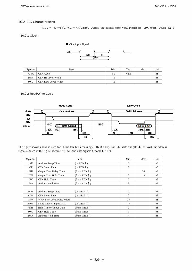
NOVA electronics Inc. MCX512 - 229
- 229 -
10.2 AC Characteristics
(TOPR = -40~+85, VDD = +3.3V±10%, Output load condition:D15~D0, INTN:85pF, SDA:400pF, Others:50pF)
10.2.1 Clock
Symbol Item Min. Typ. Max. Unit tCYC CLK Cycle 50 62.5 nS tWH CLK Hi Level Width 15 nS tWL CLK Low Level Width 15 nS
10.2.2 Read/Write Cycle
The figure shown above is used for 16-bit data bus accessing (H16L8 = Hi). For 8-bit data bus (H16L8 = Low), the address signals shown in the figure become A3~A0, and data signals become D7~D0.
Symbol Item Min. Max. Unit tAR Address Setup Time (to RDN↓) 0 nS tCR CSN Setup Time (to RDN↓) 0 nS tRD Output Data Delay Time (from RDN↓) 24 nS tDF Output Data Hold Time (from RDN↑) 0 13 nS tRC CSN Hold Time (from RDN↑) 0 nS tRA Address Hold Time (from RDN↑) 3 nS
tAW Address Setup Time (to WRN↓) 0 nS tCW CSN Setup Time (to WRN↓) 0 nS tWW WRN Low Level Pulse Width 30 nS tDW Setup Time of Input Data (to WRN↑) 10 nS tDH Hold Time of Input Data (from WRN↑) 0 nS tWC CSN Hold Time (from WRN↑) 0 nS tWA Address Hold Time (from WRN↑) 4 nS
CLK
tCYCtWH tWL
CLK Input Signal

NOVA electronics Inc. MCX512 - 230
- 230 -
10.2.3 CLK/Output Signal Timing
The following output signals are synchronized with CLK signal. The level will be changed at CLK↑.
Output signals: nPP, nPM, nDCC, nSPLTP, nPIO13~0 (according to the function selected) Symbol Item Min. Max. Unit
tDD CLK↑ → Output Signal↑↓ Delay Time 9 24 nS
Output signals: INT0N, INT1N Symbol Item Min. Max. Unit
tDD CLK↑ → INT0N, INT1N Signal↓ Delay Time 12 21 nS
10.2.4 Input Pulses
Quadrature Pulses Input Mode (A/B phases)
Up/Down Pulses Input Mode
a. In quadrature pulses input mode, when nECA, nECB input pulses are changed, the value of real position counter will be reflected
in the value of after a maximum of 4 CLK cycles. b. In UP/DOWN pulses input mode, the value of real position counter will be reflected in the value of after a maximum of 4 CLK
cycles from nPPIN, nPMIN input↑.
Symbol Item Min. Max. Unit tDE nECA, nECB Phase Difference Time tCYC +20 nS tIH nPPIN, nPMIN Hi Level Width tCYC +20 nS tIL nPPIN, nPMIN Low Level Width tCYC +20 nS
tICYC nPPIN, nPMIN Cycle tCYC×2 +20 nS tIB nPPIN↑ nPMIN↑between Time tCYC×2 +20 nS
tCYC is a cycle of CLK.
CLK
tDD
Output Signal
nECA
nECB
tDE tDE tDE tDE tDE tDE tDE tDE
Count downCount up
nPPIN
nPMIN
tIH tIL tIB tIH tIL
tICYC tICYC

NOVA electronics Inc. MCX512 - 231
- 231 -
10.2.5 General Purpose Input/Output Signals (nPIO13~0)
The figure shown at the lower left hand side illustrates the delay time when nPIO13~0 input signals are read through RR4, 5 registers. The IC built-in filter is disabled. The figure shown at the lower right hand side illustrates the delay time when writing nPIO13~0 output signals data into WR4, 5 registers.
Symbol Item Min. Max. Unit tDI Input Signal → Data Delay Time 17 nS tDO WRN↑→ Data Setup Time 35 nS
10.2.6 Split Pulse
The delay time from the rising edge of the drive pulse that starts the split pulse to when the split pulse becomes Hi (Split pulse is positive logic). When with starting pulse, only the first split pulse is output together with the drive pulse. The second or later split pulses are output with 1 CLK delay from the drive pulse. When without starting pulse, all the split pulses are output with 1 CLK delay from the drive pulse. When with starting pulse is enabled in split pulse mode setting This is, when with starting pulse is enabled in split pulse mode setting, the delay time from the rising edge of the drive pulse that starts the split pulse to when the split pulse becomes Hi. tDS1 is the delay time of the first split pulse. tDS2 indicates the delay time of the second or later split pulses. The second or later split pulses are output with 1 CLK delay.
Symbol Item Min. Max. Unit tDS1 nPP, nPM↑ → nSPLTP↑ Delay Time 20 nS tDS2 nPP, nPM↑ → nSPLTP↑ Delay Time tCYC +20 nS
tCYC is a cycle of CLK. When without starting pulse is enabled in split pulse mode setting This is, when without starting pulse is enabled in split pulse mode setting, the delay time from the rising edge of the drive pulse that starts the split pulse to when the split pulse becomes Hi.
Symbol Item Min. Max. Unit tDS nPP, nPM↑ → nSPLTP↑ Delay Time tCYC +20 nS
tCYC is a cycle of CLK.
Input signal
RDN
D15~0
tDIPIO13~0
tDO
WRN
D15~0
tDS1
nPP,nPM
nSPLTP ・・・
tDS2 tDS2
・・・ ・・・
nPP,nPM
nSPLTP
tDS
CLK
tDS

NOVA electronics Inc. MCX512 - 232
- 232 -
10.2.7 I2C Serial Bus (At fast mode.)
SCL Clock
Symbol Item Min. Max. Unit fSCL SCL Clock Frequency 400 KHz tSWH SCL Clock Hi Level Width 600 nS tSWL SCL Clock Low Level Width 1300 nS tSCR SCL Clock Time of rising edge 300 nS tSCF SCL Clock Time of falling edge 300 nS
Start/Stop Condition
Symbol Item Min. Max. Unit tSSU Start Condition Setup Time 600 nS tSHD Start Condition Hold Time 600 nS tPSU Stop Condition Setup Time 600 nS
Writing/Reading SDA Data
Symbol Item Min. Max. Unit tDIH SDA Input Hold Time 0 nS tDIS SDA Input Setup Time 100 nS
tDOD SDA Output Delay Time 0 900 nS
SCL
SDA(Input)
SDA(Output)
tDIStDIH
tDOD
tSCR tSCF
tSWH tSWL
SCL
SCL
SDA
Start Condition Stop Condition
tSSU tSHD tPSU

NOVA electronics Inc. MCX512 - 233
- 233 -
11. Timing of Input/Output Signals
11.1 Power-On Reset
a. The reset signal input to pin RESETN needs to keep on the Low level for at least 8 CLK cycles. b. When RESETN is on the Low level for 6 CLK cycles maximum, the power-on output signal is determined to the level shown
in the figure above. c. For a maximum of 4 CLK cycles after RESETN is on the Hi level, this IC cannot be read/written. 11.2 Timing of drive start/finish
a. Drive status output signal (nDRIVE) is on Hi level after a maximum of 2 CLK cycles from WRN↑when a driving command is written. And it returns to Low level after 1 CLK cycle from when the cycle of final pulse output has finished.
b. Driving pulses (nPP, nPM and nPLS) shown above are positive logic pulses. The first driving pulse will be output after a maximum of 4 CLK cycles from WRN↑when a driving command is written.
c. ASND, CNST and DSND are on valid level after 3 CLK cycles from nDRIVE↑and they return to Low level after 1 CLK cycle
from nDRIVE↓. d. When in 1-pulse 1-direction type, nDIR (direction) signal is valid after 1 CLK cycle from nDRIVE↑and keeps its level until
the next command is written after the driving is finished. e. The first pulse of the drive pulse (nPLS) will be output after 1 CLK cycle from when nDIR (direction) signal is valid.
1st Pulse 2nd Pulse Final pulse
CLK
WRN
nPP,nPM,
nDRIVE
ASND,Valid LevelCNST,
Writing a drive command
a
b
c
DSND
nDIR Valid Leveld
e
nPLS a
Pre-state
c

NOVA electronics Inc. MCX512 - 234
- 234 -
11.3 Interpolation Driving
a. The first pulses (nPP, nPM and nPLS) during interpolation driving will be output after a maximum of 4 CLK cycles from WRN↑when a driving command is written.
b. nDRIVE will become Hi level after a maximum of 2 CLK cycles from WRN↑.
c. When in 1-pulse 1-direction type, nDIR (direction) signal is on valid level while Hi level pulse is being output and the period of 1CLK cycle before and after the output (when drive pulse is positive logic).
11.4 Start Driving after Hold Command
a. The first pulse (nPP, nPM and nPLS) of each axis will be output after a maximum of 4 CLK cycles from WRN↑when a start driving after hold command is written.
b. nDRIVE will become Hi level after a maximum of 2 CLK cycles from WRN↑when a driving command of each axis is written.
11.5 Instant Stop
The following figure illustrates the timing of instant stop. Instant stop input signals are EMGN, nLMTP/M (When setting the instant stop mode) and nALARM. When an instant stop input signal becomes active, or an instant stop command is written, the output of pulses will be stopped instantly after the output of pulses being outputted.
An instant stop input signal requires a pulse width of 2 CLK cycles or more even if the input signal filter is disabled. When the input signal filter is enabled, the input signal will be delayed according to the time constant of the filter.
1st Pulse 2nd Pulse Final pulse
CLK
WRN
nPP,nPM,
nDRIVE
a
b
c
nDIR Valid Level
nPLS
undefined
cc c c cc
undefined Valid Level Valid Level
Start driving after hold commandDrive command
CLK
WRN
nPP,nPM,nPLS
nDRIVE
1st Pulse 2nd Pulsea
b
CLK
Instant input stop signal
nPP,nPM
nDRIVE
Active
Instant stop command WRN
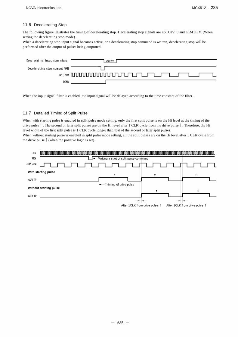
NOVA electronics Inc. MCX512 - 235
- 235 -
11.6 Decelerating Stop
The following figure illustrates the timing of decelerating stop. Decelerating stop signals are nSTOP2~0 and nLMTP/M (When setting the decelerating stop mode). When a decelerating stop input signal becomes active, or a decelerating stop command is written, decelerating stop will be performed after the output of pulses being outputted.
When the input signal filter is enabled, the input signal will be delayed according to the time constant of the filter.
11.7 Detailed Timing of Split Pulse
When with starting pulse is enabled in split pulse mode setting, only the first split pulse is on the Hi level at the timing of the drive pulse↑. The second or later split pulses are on the Hi level after 1 CLK cycle from the drive pulse↑. Therefore, the Hi level width of the first split pulse is 1 CLK cycle longer than that of the second or later split pulses. When without starting pulse is enabled in split pulse mode setting, all the split pulses are on the Hi level after 1 CLK cycle from the drive pulse↑(when the positive logic is set).
Decelerating input stop signal
nPP,nPM
DSND
Active
Decelerating stop command WRN
CLK
WRN
nPP,nPM
Without starting pulse
With starting pulse
nSPLTP
Writing a start of split pulse command
nSPLTP
↑timing of drive pulse
After 1CLK from drive pulse ↑ After 1CLK from drive pulse ↑
1
1 2 3
2

NOVA electronics Inc. MCX512 - 236
- 236 -
12. Package Dimensions
Package Size 14×14×1.4 mm
Symbol Size (mm)
Description Min. Standard Max.
A - - 1.7 Height from seating plane to the top end of package main unit A1 - 0.1 - Height from seating plane to the bottom end of package main unit A2 - 1.4 - Height from the top end to the bottom end of package main unit b 0.17 - 0.27 Pin width c 0.09 - 0.2 Pin thickness D 15.6 16 16.4 Overall length including pin length D1 13.9 14 14.1 Length of package main unit E 15.6 16 16.4 Overall width including pin length E1 13.9 14 14.1 Width of package main unit e 0.5 Pin pitch L 0.3 - 0.75 Length of the pin flat section contacting seating plane θ 0゜ - 10゜ Angle of the pin flat section to seating plane
aaa 0.08 Uniformity of the bottom of pins (permissible value in the vertical direction)
25
26100
76
75 51
50
1
e b
D
D1
EE1
A
A2
A1
cL
Section A aaa
Installation Face
Details of Section A
INDEX
NOVA elec.MCX512
Section A

NOVA electronics Inc. MCX512 - 237
- 237 -
13. Storage and Recommended Installation Conditions
13.1 Storage of this IC
Note the following items in regard to the storage of this IC. (1) Do not throw or drop the IC. Otherwise, the packing material could be torn, damaging the airtightness. (2) Store the IC sealed damp-proof package in the temperature 30°C or lower and humidity 85%RH or lower and use the IC within
12 months. (3) If the IC usage date has expired, remove any dampness by baking it at the temperature 125°C±5°C for 20 hours or more and
30 hours or less. The number of baking must not exceed two times. If damp-proofing is damaged before expiration, also apply damp removal processing.
(4) Protect the device from static electricity before applying damp removal processing. (5) After opening the damp-proof package, store the IC in the temperature 30°C or lower and humidity 70%RH or lower, and install
it within seven days. If the allowable storage period described above has been exceeded, baking must be applied before installation of the IC.
13.2 Standard Installation Conditions by Soldering Iron
The standard installation conditions for the IC by soldering iron are as follows. (1) Installation method: Soldering iron (heating pin section) (2) Installation conditions: The temperature of the pin: 350°C or lower, Time: 5 seconds or less, Number of times: 2 times or less
13.3 Standard Installation Conditions by Solder Reflow
The standard installation conditions for the IC by solder reflow are as follows.
MCX512 Standard Soldering Reflow Heat-proof Profile
Time (second)
250
220
200
140
60~120seconds Max60seconds
Preheating
Pac
kage
Sur
face
Tem
pera
ture
()
Mainheating
Max10seconds
Time of 140~200 (Preheating temperature)
Solder reflow count
Time of over 250
Maximum reflow temperature (package surface temperature) 260 or less
10 seconds or less
60~120 seconds
Up to twice
260
Time of over 220 60 seconds or less
Mounting Method(1) Infrared(2) Hot air(3) Infrared and Hot air

NOVA electronics Inc. MCX512 – A-1
-A-1-
Appendix A Calculation Formula of Acceleration/Deceleration Drive
A-1 Case of Trapezoidal Acceleration/Deceleration Driving
(CLK = 16MHz)
Calculation Formula of acceleration AC when initial speed SV, drive speed DV and acceleration time ta are given
Acceleration at
SVDVAC
−= [pps/sec]
Calculation Formula of acceleration time ta when initial speed SV, drive speed DV and acceleration AC are given
Acceleration time AC
SVDVta
−= [sec]
Calculation Formula of pulse number for acceleration Pa when initial speed SV, drive speed DV and acceleration AC are given
Pulse number for acceleration AC2
SVDVP
22
a×−
=
Deceleration DC, deceleration time td and pulse number for deceleration Pd can be calculated by replacing acceleration AC, acceleration time ta and pulse number for acceleration Pa with deceleration DC, deceleration time td and pulse number for deceleration Pd respectively. [Note]
• The above calculation formula is an ideal expression and slight differences will be made in the actual IC operation.
DV: Drive speed[pps] SV: Initial speed[pps] AC: Acceleration[pps/sec] ta: Acceleration time [sec] Pa: Pulse number for acceleration

NOVA electronics Inc. MCX512 – A-2
-A-2-
A-2 Case of S-curve Acceleration/Deceleration Driving (CLK = 16MHz)
Acceleration AC is fixed to 1FFF FFFFh.
Calculation Formula of jerk JK when initial speed SV, drive speed DV and acceleration time ta are given
Jerk 2
at
)SVDV(4JK
−= [pps/sec2]
Calculation Formula of acceleration time ta when initial speed SV, drive speed DV and jerk JK are given
Acceleration time JK
SVDV2ta
−= [sec]
Calculation Formula of pulse number for acceleration Pa when initial speed SV, drive speed DV and jerk JK are given
Pulse number for acceleration JK
SVDV)SVDV(Pa
−+=
Deceleration increasing rate DJ, deceleration time td and pulse number for deceleration Pd can be calculated by replacing jerk JK, acceleration time ta and pulse number for acceleration Pa with deceleration increasing rate DJ, deceleration time td and pulse number for deceleration Pd respectively. [Note]
• The above calculation formula does not hold true in partial S-curve acceleration/deceleration driving. • The above calculation formula is an ideal expression and slight differences will be made in the actual IC operation.
DV: Drive speed[pps] SV: Initial speed[pps] JK: Jerk[pps/sec2] ta: Acceleration time [sec] Pa: Pulse number for acceleration

NOVA electronics Inc. MCX512 – B-1
-B-1-
Appendix B Parameter Calculation Formula when Input Clock except
16MHz When MCX512 input clock frequency is fCLK (Hz), setting values of each speed and timer are as follows.
Initial speed [pps] = 6
CLK
1016
fSV
××
Drive speed [pps] = 6
CLK
1016
fDV
××
Acceleration [pps/sec] =
2
6
CLK
1016
fAC
×
×
Deceleration [pps/sec] =
2
6
CLK
1016
fDC
×
×
Jerk [pps/sec2] =
3
6
CLK
1016
fJK
×
×
Deceleration increasing rate [pps/sec2] =
3
6
CLK
1016
fDJ
×
×
Home search speed [pps] = 6
CLK
1016
fHV
××
Speed increasing/decreasing value [pps] = 6
CLK
1016
fIV
××
Timer value [μsec] = CLK
6
f
1016TM
××
[Symbol]
SV: Initial speed setting DV: Drive speed setting AC: Acceleration setting DC: Deceleration setting JK: Jerk setting DJ: Deceleration increasing rate setting HV: Home search speed setting IV: Speed increasing/decreasing value setting TM: Timer value setting
Synchronous pulse output width (synchronous action), deviation counter clear output signal width (automatic home search), timer time between steps (automatic home search) and input signal delay time (input signal filter) require correction by using
CLK
6
f
1016 × respectively.

NOVA electronics Inc. MCX512 – C-1
-C-1-
Appendix C Differences with MCX300 series Main differences between MCX300 series and MCX512 are as follows. For details of functions, please refer to each description in this manual.
Item MCX300 series MCX512 1 Treatment of unused
input pins Can open. (pulled up to VDD in the IC)
There are input pins not pulled up in the IC, which should be connected to VDD or GND. See chapter 5 for more details.
2 Width of reset signal (RESETN)
Requires more than 4 CLK cycles Requires more than 8 CLK cycles
3 Command reset Writes 8000h (D15 bit:1) into WR0 register. Writes 00FFh into WR0 register. 4 Setting of speed
parameter Speed range setting is provided. (multiple:1~500)
Speed parameter should be set based on the actual value and multiple.
No speed range setting (speed range-free) Speed parameter is set the actual value.
5 Fixed pulse driving ・ +Direction fixed pulse driving Specifies output pulse number by positive value. When executed, it drives specified pulses in the +direction.
・ -Direction fixed pulse driving Specifies output pulse number by positive value. When executed, it drives specified pulses in the -direction.
・ Relative position driving Specifies output pulse number by positive value and when executed, it drives specified pulses in the +direction. Specifies output pulse number by negative value and when executed, it drives specified pulses in the -direction.
・ Counter relative position driving Specifies output pulse number by positive value and when executed, it drives specified pulses in the -direction. This is a driving command corresponding to - direction fixed pulse driving of MCX300 series.
・ Absolute position driving As the finish point of driving, specifies logical position counter value that is a destination point
6 RR2 register/Error information display (Software limit and hardware limit signal, alarm signal from a servo driver and emergency stop signal)
Even though driving stops, if error factor becomes active, error information bit becomes 1. And when error factor is cleared, error information bit returns to 0.
If error factor becomes active during the driving (or error factor is active at the start of driving), error information bit becomes 1 and will keep 1 even after error factor is cleared. If error factor becomes active while driving stops, it does not become error. All the bits of RR2 return to 0 by error/finishing status clear command (79h) or the start of next driving. However, when an error occurs during interpolation driving, it is necessary to write error/finishing status clear command (79h) after checking that interpolation drive stops.
7 Enable/disable of hardware limit function
Function of hardware limit signals (nLMTP and nLMTM) (LMT+ and LMT- in MCX305) cannot be disabled.
Function of hardware limit signals (nLMTP and nLMTM) can be enabled/disabled.
8 Setting of software limit value
Sets software limit value to compare register (COMP+, COMP-) Because of this, when using compare register as software limit, the other function of compare register cannot be used.
Sets software limit value to a dedicated register (SLMT+, SLMT-).
9 Stop type of software limit
Only decelerating stop Selectable from decelerating stop or instant stop.
10 Trapezoid triangle form prevention
At reset:Disabled At reset:Enabled
11 Acceleration counter offsetting
At reset:8 At reset:0
12 Command code and mode setting bit
- Differs from MCX300 series.

NOVA electronics Inc. MCX512 – C-2
-C-2-
13 Position and speed
parameters setting for interpolation driving
When interpolation driving is performed continuously, and if parameters are the same as previous values, it is not necessary to set them again.
Before writing interpolation drive command, be sure to set position and speed parameters. When parameters are the same as previous values, it is necessary to set them again.
14 How to set 2-axis constant vector speed
Mode setting: Set to WR5/D8, D9 Mode setting: Interpolation mode setting command (2Ah) Set to WR6/D6, D7
Speed range setting: Set the value that multiplies the range of main axis by 1.414 to the range of second axis.
Not required
15 Single-step interpolation
Can be performed by commands and the external signal.
Can be performed by commands only.