Lecture UG1 Introduction to Packaging - TheCATweb.cecs.pdx.edu/~jmorris/TKK/Lecture UG1... ·...
33
4/6/2009 1 Electronics Packaging TKK 2009 L 1 James E. Morris Dept of Electrical & Computer Engineering TKK 2009 Lecture 1 Portland State University Tuesday Lecture Friday Lecture Electronics Packaging Tuesday Lecture Friday Lecture April 7: Introduction April 17: Electrical Package Design April 21: Package Reliability April 24: Electrically Conductive Adhesives I April 28: Electrically Conductive Adhesives II 7 April 2009 Electronics Packaging TKK 2009 2 Download course notes from: http://www.ece.pdx.edu/~jmorris/TKK/UG e-mail: [email protected]
Transcript of Lecture UG1 Introduction to Packaging - TheCATweb.cecs.pdx.edu/~jmorris/TKK/Lecture UG1... ·...

4/6/2009
1
Electronics PackagingTKK 2009 L 1
James E. MorrisDept of Electrical & Computer
Engineering
TKK 2009 Lecture 1
Portland State University
Tuesday Lecture Friday Lecture
Electronics Packaging
Tuesday Lecture Friday Lecture
April 7: Introduction
April 17: Electrical Package Design
April 21: Package Reliability April 24: Electrically Conductive Adhesives I
April 28: Electrically Conductive Adhesives II
7 April 2009 Electronics Packaging TKK 2009 2
Download course notes from: http://www.ece.pdx.edu/~jmorris/TKK/UG
e-mail: [email protected]

4/6/2009
2
ReferencesR. Ulrich & W.D.Brown (editors)
“Advanced Electronic Packaging, 2nd edition” Wiley/IEEE Press (2005)
Tummala (editor) “Fundamentals of Microsystems Packaging” McGraw Hill (2001)McGraw-Hill (2001)
Pecht et al “Integrated Circuit, Hybrid, & MCM Packaging Design Guidelines” Wiley (1994)J.E. Morris (editor) “Electronics Packaging Forum: Vols 1 & 2” VNR (1990) J.E. Morris (editor) “Electronics Packaging Forum: MCM Issues” IEEE Press (1994)
7 April 2009Electronics Packaging TKK 2009 3
IEEE Press (1994)
Johan Liu (editor) “Conductive Adhesives for Electronics Packaging” Electrochemical (1999)
Lecture 1 Introduction
The package roadblock to system performance
What is packaging?
7 April 2009Electronics Packaging TKK 2009 4
Packaging technologies

4/6/2009
3
7 April 2009Electronics Packaging TKK 2009 5
Borsuk & Coffey, Defense Horizons
7 April 2009Electronics Packaging TKK 2009 6
4/6/2009
4
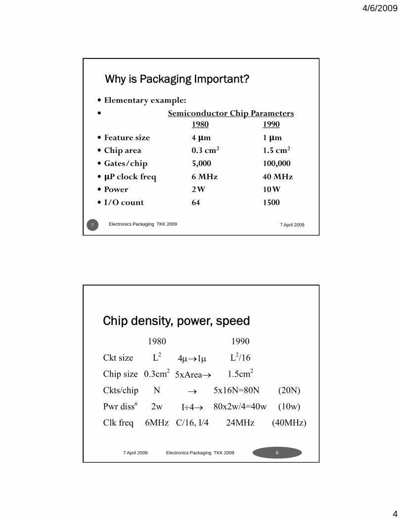
Why is Packaging Important?
Elementary example:
Semiconductor Chip Parametersp1980 1990
Feature size 4 μm 1 μmChip area 0.3 cm2 1.5 cm2
Gates/chip 5,000 100,000
μP clock freq 6 MHz 40 MHz
7 April 2009Electronics Packaging TKK 2009 7
μP clock freq 6 MHz 40 MHzPower 2 W 10 W
I/O count 64 1500
Chip density, power, speed
1980 19901980 1990
Ckt size L2 4μ→1μ L2/16
Chip size 0.3cm2 5xArea→ 1.5cm2
Ckts/chip N → 5x16N=80N (20N)
P di n 2 80 2 /4 40 (10 )Pwr dissn 2w I÷4→ 80x2w/4=40w (10w)
Clk freq 6MHz C/16, I/4 24MHz (40MHz)
7 April 2009 Electronics Packaging TKK 2009 8

4/6/2009
5
ITRS product categoriesProduct category Product description
Low cost <$ 300: consumer products, microcontrollers, disk drivers
Hand-held <$ 1000: battery powered products e.g. mobile and cellular products
Cost/performance <$3000: notebooks, desktop personal computers
High performance >$3000:high-end work stations, servers, avionics,
7 April 2009Electronics Packaging TKK 2009 9
supercomputer
Harsh environment Under-the-hood and other hostile environment products
Memory DRAM’s, SRAM’s
ITRS Packaging requirements
7 April 2009Electronics Packaging TKK 2009 10

4/6/2009
6
Semi-log Moore's plots of the Road-map data
7 April 2009Electronics Packaging TKK 2009 11
Rent’s Rule
7 April 2009Electronics Packaging TKK 2009 12

4/6/2009
7
Rent’s rule plot of roadmap data
7 April 2009Electronics Packaging TKK 2009 13
Pkg pins ≈ Kp(bits or gates)β
β Kβ Kp
SRAM 0.12 6μP 0.45 0.82Gate array 0.50 1.9Computr:chip 0.63 1.4Computr:syst 0.25 82
7 April 2009 Electronics Packaging TKK 2009 14

4/6/2009
8
Rent’s Rule
7 April 2009Electronics Packaging TKK 2009 15
Example I/O
Package 1980 1990Package 1980 64-pin DIL0.1in pitch3.3x1.0in2
19901500-pin QFP0.01in pitch3.75x3.75in2
Pkg I/O 64 pins Rent’s rule→ 1500 pins
Chip: 0 6x0 5cm2 1 25x1 2cm2Chip: 0.6x0.5cm 1.25x1.2cm
I/O pitch 344 μm 33 μm
7 April 2009 Electronics Packaging TKK 2009 16

4/6/2009
9
Clock Frequency vs Time
7 April 2009Electronics Packaging TKK 2009 17
Bare and packaged chip speeds
7 April 2009Electronics Packaging TKK 2009 18
4/6/2009
10
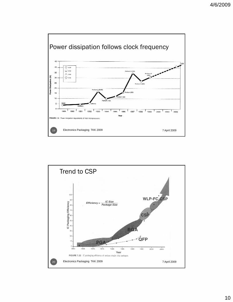
Power dissipation follows clock frequency
7 April 2009Electronics Packaging TKK 2009 19
Trend to CSP
7 April 2009Electronics Packaging TKK 2009 20

4/6/2009
11
Package functions
7 April 2009Electronics Packaging TKK 2009 21
Electronics Packaging is Multi-disciplinary!Electrical
ArchitecturesPower distribution
MaterialsMetallurgyCeramics
EMI/EMC, crosstalk, ΔI & switching noise
MechanicalVibrationsStress
ThermalC d l
PolymersSurface scienceInterfaces/diffusion
ManufacturingInstrumentationProcess control
f b l / T
7 April 2009Electronics Packaging TKK 2009 22
Conduction coolingConvection cooling
Manufacturability/ Test

4/6/2009
12
Packaging Levels
7 April 2009Electronics Packaging TKK 2009 23
Lead Pitch/Density: peripheral leads, area array, 3D
7 April 2009Electronics Packaging TKK 2009 24

4/6/2009
13
PWB Density
7 April 2009Electronics Packaging TKK 2009 25
PWB line width, pitch, & pin-count
7 April 2009Electronics Packaging TKK 2009 26

4/6/2009
14
Electronics Packaging
Electronics packaging covers all technologies involved in device manufacture and design from the chip to the board. In modern d i it i ll th k hi h li it t f d devices, it is usually the package which limits system performance, and its cost can greatly exceed the cost of the silicon chip it supports. Packaging engineers are much in demand, therefore, due also to the fact that the field’s inherently multi-disciplinary nature creates a shortage of qualified people. Modern practice calls for chip/package co-design, making an understanding of packaging principles a must for all IC designers
7 April 2009Electronics Packaging TKK 2009 27
all IC designers.
Lecture Objectives
Introduce first-level interconnect technologies:wire bond & flip chip wire-bond & flip-chip
Introduce standard SMT & PTH packages(surface mount technology & pin through hole)
Introduce MCM, COB, DCA, CSP, WLP, etc (multi-chip modules, chip on board, direct chip attach, chip-scale package, wafer-level packaging)
7 April 2009Electronics Packaging TKK 2009 28
p g p g g
Introduce basic packaging acronyms
4/6/2009
15
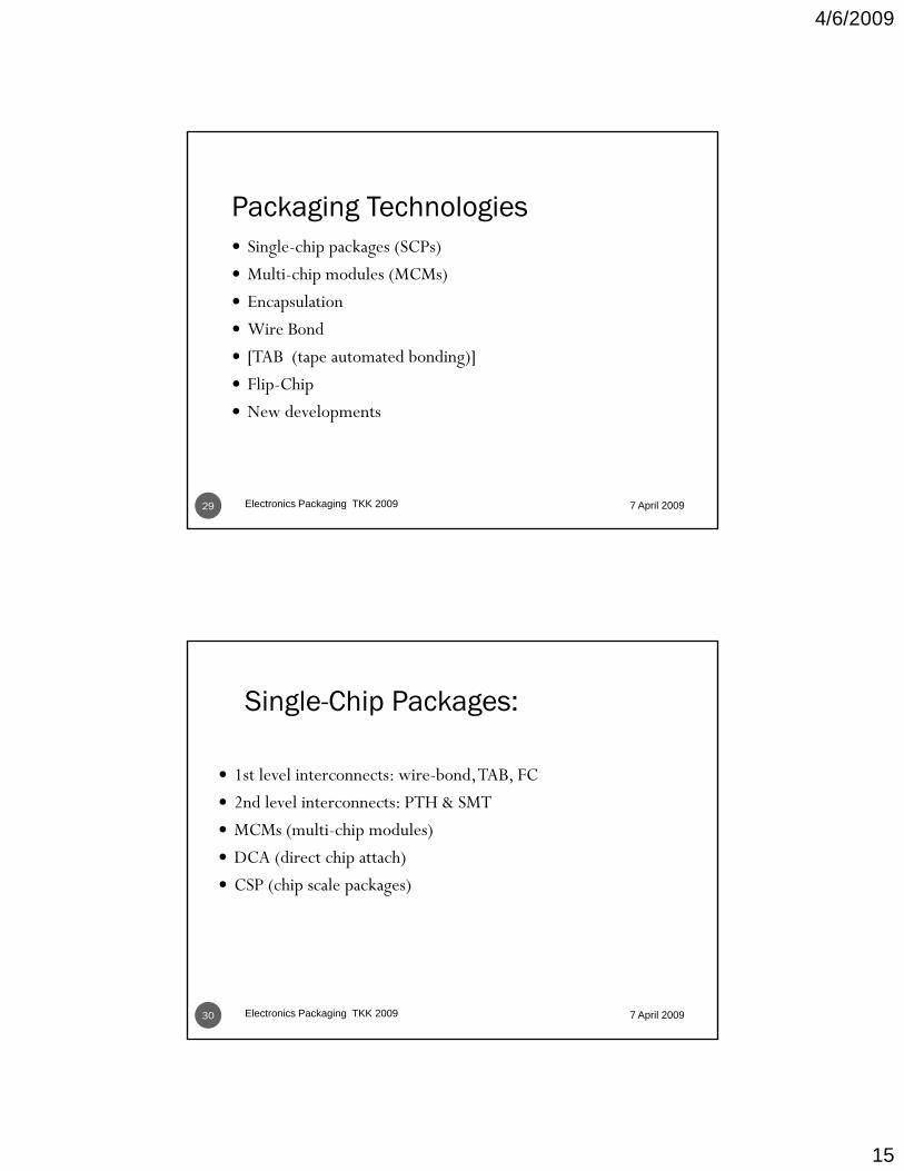
Packaging TechnologiesSingle-chip packages (SCPs)
Multi-chip modules (MCMs)
Encapsulation
Wire Bond
[TAB (tape automated bonding)]
Flip-Chip
7 April 2009Electronics Packaging TKK 2009 29
New developments
Single-Chip Packages:
1st level interconnects wire bond TAB FC1st level interconnects: wire-bond, TAB, FC
2nd level interconnects: PTH & SMT
MCMs (multi-chip modules)
DCA (direct chip attach)
CSP (chip scale packages)
7 April 2009Electronics Packaging TKK 2009 30

4/6/2009
16
First-level interconnect
7 April 2009Electronics Packaging TKK 2009 31
Wirebond TAB Flip-chip(Tape-automated bonding)
7 April 2009Electronics Packaging TKK 2009 32

4/6/2009
17
7 April 2009Electronics Packaging TKK 2009 33
PTH
PGA
SMT:J l dJ-leadGull-wingLeadless
COB/DCAflip-chipTAB
7 April 2009Electronics Packaging TKK 2009 34
TAB

4/6/2009
18
7 April 2009Electronics Packaging TKK 2009 35
7 April 2009Electronics Packaging TKK 2009 36

4/6/2009
19
Second-level package attach
7 April 2009Electronics Packaging TKK 2009 37SMT & PTH
Substrate Vias
PCB (printed circuit board) or PWB (printed wiring board)
7 April 2009Electronics Packaging TKK 2009 38
Multi-layer laminate
Drilled, electroplated Cu
Copper paste (ALIVH), silver loaded (ECA) epoxies, etc
4/6/2009
20
7 April 2009Electronics Packaging TKK 2009 39
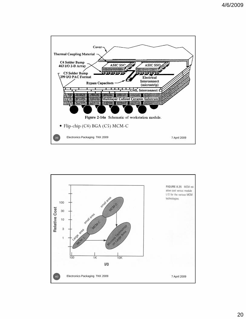
Flip-chip (C4) BGA (C5) MCM-C
7 April 2009Electronics Packaging TKK 2009 40

4/6/2009
21
7 April 2009Electronics Packaging TKK 2009 41
7 April 2009Electronics Packaging TKK 2009 42

4/6/2009
22
Encapsulation: “Glob-top”
7 April 2009Electronics Packaging TKK 2009 43
COB/DCA encapsulation
7 April 2009Electronics Packaging TKK 2009 44 Syringe dispense

4/6/2009
23
Encapsulation: Cavity-fill
7 April 2009Electronics Packaging TKK 2009 45
Encapsulation: Transfer molding
7 April 2009Electronics Packaging TKK 2009 46

4/6/2009
24
Encapsulation: Underfill
7 April 2009Electronics Packaging TKK 2009 47
7 April 2009Electronics Packaging TKK 2009 48

4/6/2009
25
Dual-in-line (DIL) plastic package (DIP)
Wire-bonding
7 April 2009Electronics Packaging TKK 2009 49
7 April 2009Electronics Packaging TKK 2009 50

4/6/2009
26
7 April 2009Electronics Packaging TKK 2009 51
7 April 2009Electronics Packaging TKK 2009 52

4/6/2009
27
7 April 2009Electronics Packaging TKK 2009 53
7 April 2009Electronics Packaging TKK 2009 54

4/6/2009
28
7 April 2009Electronics Packaging TKK 2009 55
Wire sweep
7 April 2009Electronics Packaging TKK 2009 56

4/6/2009
29
Wafer bumping
7 April 2009Electronics Packaging TKK 2009 57
Solder bumps
As printed →As printed →
Re-flowed →
7 April 2009Electronics Packaging TKK 2009 58

4/6/2009
30
7 April 2009Electronics Packaging TKK 2009 59
7 April 2009Electronics Packaging TKK 2009 60

4/6/2009
31
7 April 2009Electronics Packaging TKK 2009 61
WLP & Redistribution
7 April 2009Electronics Packaging TKK 2009 62

4/6/2009
32
7 April 2009Electronics Packaging TKK 2009 63
7 April 2009Electronics Packaging TKK 2009 64
4/6/2009
33
Lecture Summary
Standard packagesEncapsulation
First level interconnect (chip to package):Wire-bond, TAB, flip-chip (C4)
Second-level interconnect (package to board):PTH, SMT, PGA, BGA (C4/C5), etc
MCMs, CSPs, WLP, etc
7 April 2009Electronics Packaging TKK 2009 65
C , CS , ,


![PeopleBot - TheCATweb.cecs.pdx.edu/.../PeopleBot_ProjectReport[1]-Dubay2010.pdf · This multi-threaded module is implemented in JAVA ... of PeopleBot. The softwares used and the AI](https://static.fdocuments.us/doc/165x107/5aa7f8c67f8b9ab8228cf06f/peoplebot-1-dubay2010pdfthis-multi-threaded-module-is-implemented-in-java-.jpg)