Lecture 5 Combinational Logic Implementation Using Multiplexers, ROMS, FPGAs
42
ECE C03 Lecture 5 1 Lecture 5 Combinational Logic Implementation Using Multiplexers, ROMS, FPGAs Prith Banerjee ECE C03 Advanced Digital Logic Design Spring 1998
-
Upload
noelle-mcdowell -
Category
Documents
-
view
33 -
download
2
description
Lecture 5 Combinational Logic Implementation Using Multiplexers, ROMS, FPGAs. Prith Banerjee ECE C03 Advanced Digital Logic Design Spring 1998. Outline. Combinational Logic Implementations Multiplexers Decoders ROMS Field Programmable Logic Arrays - PowerPoint PPT Presentation
Transcript of Lecture 5 Combinational Logic Implementation Using Multiplexers, ROMS, FPGAs
ECE C03 Lecture 5 1
Lecture 5Combinational Logic Implementation Using Multiplexers, ROMS, FPGAs
Prith Banerjee
ECE C03
Advanced Digital Logic Design
Spring 1998

ECE C03 Lecture 5 2
Outline
• Combinational Logic Implementations• Multiplexers• Decoders• ROMS• Field Programmable Logic Arrays• READING: Katz 4.2.2, 4.2.3, 4.2.4, 4.2.5, 10.3,
Dewey 5.7
ECE C03 Lecture 5 3
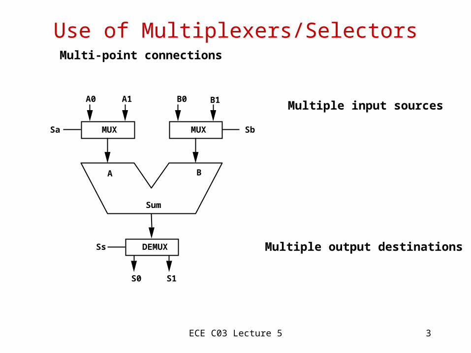
Use of Multiplexers/SelectorsMulti-point connections
MUX MUX
DEMUX
A B
Sum
A0 A1 B0 B1
Sa Sb
Ss
S0 S1
Multiple input sources
Multiple output destinations

ECE C03 Lecture 5 4
I 1 0 0 0 0 1 1 1 1
I 0 0 0 1 1 0 0 1 1
A 0 1 0 1 0 1 0 1
Z 0 0 1 0 0 1 1 1
A 0 1
Z I 0 I 1
General Concept of Using Multiplexers2 data inputs, n control inputs, 1 output
used to connect 2 points to a single point
control signal pattern form binary index of input connected to output
n
n
Two alternative formsfor a 2:1 Mux Truth Table
Z = A' I + A I0 1
Functional form
Logical form

ECE C03 Lecture 5 5
Use of Multiplexers/SelectorsZ = A' I + A I0 1
Z = A' B' I0 + A' B I1 + A B' I2 + A B I3
Z = A' B' C' I0 + A' B' C I1 + A' B C' I2 + A' B C I3 + A B' C' I4 + A B' C I5 + A B C' I6 + A B C I7
In general, Z = m I2 -1n
k=0 k kin minterm shorthand form for a 2 :1 Muxn
2:1 mux
I 0
I 1
A
Z
I 0
A
I 1 I 2 I 3
B
Z 4:1 mux
I 0
A
I 1 I 2 I 3
B
Z 8:1
mux
C
I 4 I 5 I 6
I 7
ECE C03 Lecture 5 6
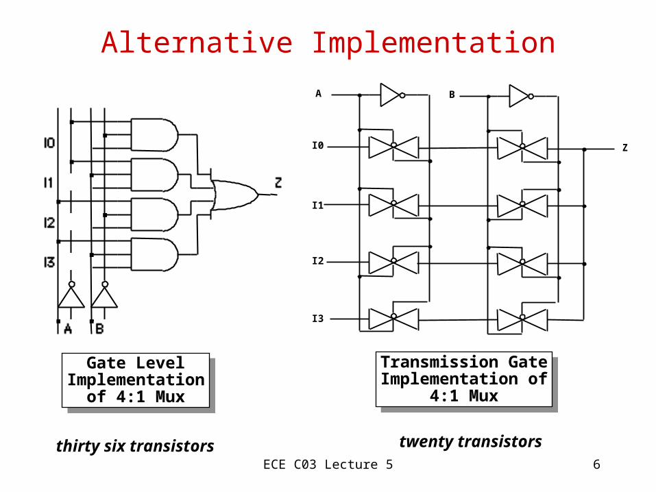
Alternative Implementation
Gate LevelImplementation
of 4:1 Mux
Gate LevelImplementation
of 4:1 Mux
Transmission GateImplementation of
4:1 Mux
Transmission GateImplementation of
4:1 Mux
thirty six transistors twenty transistors
I3
I0
I2
I1
A B
Z

ECE C03 Lecture 5 7
Design of Large MultiplexersLarge multiplexers can be implemented by cascaded smaller ones
Control signals B and C simultaneouslychoose one of I0-I3 and I4-I7
Control signal A chooses which of theupper or lower MUX's output to gate to Z
0
1 S
0
1 S
0
1 S
0
1 S
0
1
S1
2
3 S0
C
A B
I 0
I 1
I 2
I 3
I 4
I 5
I 6
I 7
C
C
C
ZAlternative 8:1 Mux Implementation
4:1 mux
4:1 mux
8:1 mux
2:1 mux
0 1 2 3
0 1 2 3
S
S 1 S 0
S 1 S 0
Z
A C B
I 0 I 1 I 2 I 3
I 4 I 5 I 6 I 7
0
1

ECE C03 Lecture 5 8
Multiplexers/Selectors as General Purpose Blocks
2 :1 multiplexer can implement any function of n variables
n-1 control variables; remaining variable is a data input to the mux
n-1
Example:
F(A,B,C) = m0 + m2 + m6 + m7
= A' B' C' + A' B C' + A B C' + A B C
= A' B' (C') + A' B (C') + A B' (0) + A B (1)
8:1 MUX
1 0 1 0 0 0 1 1
0 1 2 3 4 5 6 7 S2 S1 S0
A B C
F
"Lookup Table"
S1 S0
A B
4:1 MUX
0 1 2 3
C
C01
F
A 0 0 0 0 1 1 1 1
B 0 0 1 1 0 0 1 1
C 0 1 0 1 0 1 0 1
F 1 0 1 0 0 0 1 1
C
C
0
1

ECE C03 Lecture 5 9
I 1
1 1
1
1 0
I n
0 1
I n
0 0
0
… F I 2 I n
0
1 …
Generalization of Multiplexer/Selector Logic
n-1 Mux control variables
single Muxdata variable
Four possibleconfigurations
of the truth table rows
Can be expressed asa function of In, 0, 1
Example:G(A,B,C,D) can be implemented by an 8:1 MUX:
K-mapChoose A,B,C
as control variables
MultiplexerImplementation
TTL package efficientMay be gate inefficientTTL package efficientMay be gate inefficient
G 8:1 mux
0 1 2 3 4 5 6 7
A B C
S 2 S 1 S 0
1 D 0 1 D D D D

ECE C03 Lecture 5 10
Decoders/DemultiplexersDecoder: single data input, n control inputs, 2 outputs
control inputs (called select S) represent Binary index of output to which the input is connected
data input usually called "enable" (G)
n
1:2 Decoder:
O0 = G • S; O1 = G • S
2:4 Decoder:
O0 = G • S0 • S1
O1 = G • S0 • S1
O2 = G • S0 • S1
O3 = G • S0 • S1
3:8 Decoder:O0 = G • S0 • S1 • S2
O1 = G • S0 • S1 • S2
O2 = G • S0 • S1 • S2
O3 = G • S0 • S1 • S2
O4 = G • S0 • S1 • S2
O5 = G • S0 • S1 • S2
O6 = G • S0 • S1 • S2
O7 = G • S0 • S1 • S2

ECE C03 Lecture 5 11
Alternative Implementations
1:2 Decoder, Active High Enable 1:2 Decoder, Active Low Enable
2:4 Decoder, Active High Enable 2:4 Decoder, Active Low Enable
Output0G
Select
Output1
Output0/GSelect
Output1
Select0 Select1
Output2
Output3
Output0G
Output1
Select0 Select1
Output2
Output3
Output0/G
Output1

ECE C03 Lecture 5 12
Switch Level ImplementationsSelect
SelectSelect
Select
G Output0
Select
Select
Output1
Select
Select
"0"
"0"
Select
SelectSelect
Select
G Output
Output
0
1
Naive, Incorrect Implementation
All outputs not driven at all times
Correct 1:2 Decoder Implementation

ECE C03 Lecture 5 13
Switch Implementation of 2:4 Decoder
G Output0
"0"
"0"
Select 1Select
G Output1
"0"
"0"
0
G Output2
"0"
"0"
G Output3
"0"
"0"
Operation of 2:4 Decoder
S0 = 0, S1 = 0
one straight thru path
three diagonal paths

ECE C03 Lecture 5 14
Decoder as a Logic Building Block
Decoder Generates AppropriateMinterm based on Control Signals
Example Function:
F1 = A' B C' D + A' B' C D + A B C DF2 = A B C' D' + A B CF3 = (A' + B' + C' + D')
3:8 dec
0 1
2 3 4 5 6 7
A B C
Enb
ABC ABC ABC ABC ABC ABC
ABC ABC S 2 S 1 S 0
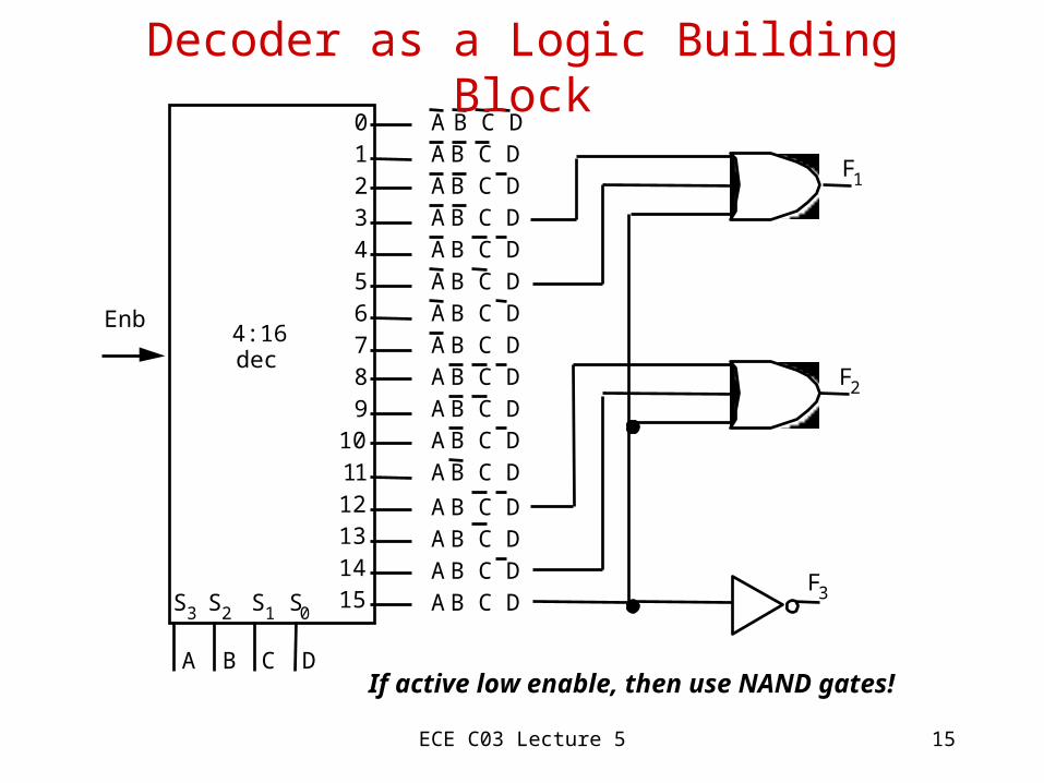
ECE C03 Lecture 5 15
A B C D A B C D A B C D A B C D A B C D A B C D A B C D A B C D A B C D A B C D A B C D A B C D
A B C D A B C D A B C D A B C D
F 1
F 3
0 1 2 3 4 5 6 7 8 9
10 1 1 12 13 14 15
A
S 3 S 2 S 1 S 0
4:16 dec
Enb
B C D
F 2
Decoder as a Logic Building Block
If active low enable, then use NAND gates!

ECE C03 Lecture 5 16
Alternative Implementation of 32:1 Mux
Multiplexer Only Multiplexer + Decoder
EN76543210CBA
151
WY
4321
15
14
11
10
9
65
B1B2B3
B0
A3A2A1A0
153GA
GB
YA
YB
S1SO
65431
10111213
15 142
7
9
EN76543210CBA
151
WY
4321
15
14
11
10
9
65
EN76543210CBA
151
WY
4321
15
14
13
11
10
9
65
EN76543210
151
WY1 6
5
S2 S1 S0
I7
F(A, B, C, D, E)
I0
I15
I23
I31
I6I5I4I3I2I1
A B
C D E
1Y21Y11Y0
1Y3139
2Y12Y0
2Y3
6543210CBA
4321
1514
11109
EN76543210
151
WY
4321
1514
11109
7
65
S2 S1 S0
I31
I0
I5I4I3I2I1
C D E
1G
1B1A2G2B2A
4567
23
1
1211109
1413
152Y2
6543210CBA
4321
1514
11109
EN76543210
151
WY
4321
1514
11109
7
65
S2 S1 S0
I23
I0
I5I4I3I2I1
C D E
6543210CBA
4321
1514
11109
EN76543210
151
WY
4321
1514
11109
7
65
S2 S1 S0
I15
I0
I5I4I3I2I1
C D E
6543210CBA
4321
1514
11109
EN76543210
151
WY
7
65
S2 S1 S0
I7
I0
I6I5I4I3I2I1
C D E
A B
F(A, B, C, D, E)

ECE C03 Lecture 5 17
5:32 Decoder
5:32 Decoder
Subsystem
\EN
S4 S3 S2 S1 S0
.
.
.
\Y31
\Y0
2Y2
1Y11Y0
1Y31Y2
2Y12Y0
2Y3
1G
1B1A
139
2G
2B2A
S4 S3
G1G2AG2B
C
BA
Y7Y6Y5Y4
Y1Y0
Y3Y2
138
G1G2AG2B
CBA
Y7Y6Y5Y4
Y1Y0
Y3Y2
138
G1G2AG2B
CBA
Y7Y6Y5Y4
Y1Y0
Y3Y2
138
G1G2AG2B
CBA
Y7Y6Y5Y4
Y1Y0
Y3Y2
138
\EN
S2 S1 S0
S2 S1 S0
S2 S1 S0
S2 S1 S0
\Y31\Y30\Y29\Y28\Y27\Y26\Y25\Y24
\Y23\Y22\Y21\Y20\Y19\Y18\Y17\Y16
\Y15\Y14\Y13\Y12\Y11\Y10\Y9\Y8
\Y7\Y6\Y5\Y4\Y3\Y2\Y1\Y0

ECE C03 Lecture 5 18
Read-Only Memories
ROM: Two dimensional array of 1's and 0's
Row is called a "word"; index is called an "address"
Width of row is called bit-width or wordsize
Address is input, selected word is output
Dec
0 n-1
Address
2 -1n
0
+5V +5V +5V +5V
Word Line 0011 Word Line 1010
Bit Lines
j
i
Internal Organization

ECE C03 Lecture 5 19
Implementing Logic with ROMs
F0 = A' B' C + A B' C' + A B' C
F1 = A' B' C + A' B C' + A B C
F2 = A' B' C' + A' B' C + A B' C'
F3 = A' B C + A B' C' + A B C'
address outputs
ROM 8 w ords ¥
4 bits
A B C F 0 F 1 F 2 F 3
B 0 0 1 1 0 0 1 1
Address W ord Contents A 0 0 0 0 1 1 1 1
C 0 1 0 1 0 1 0 1
F 0 0 1 0 0 1 1 0 0
F 1 0 1 1 0 0 0 0 1
F 2 1 1 0 0 1 0 0 0
F 3 0 0 0 1 1 0 1 0
by
ECE C03 Lecture 5 20
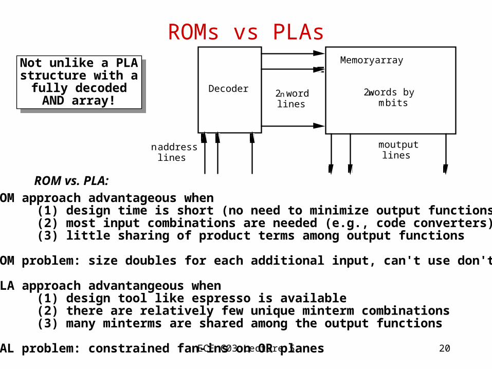
ROMs vs PLAs
Not unlike a PLAstructure with afully decoded
AND array!
Not unlike a PLAstructure with afully decoded
AND array!
ROM vs. PLA:ROM approach advantageous when (1) design time is short (no need to minimize output functions) (2) most input combinations are needed (e.g., code converters) (3) little sharing of product terms among output functions
ROM problem: size doubles for each additional input, can't use don't cares
PLA approach advantangeous when (1) design tool like espresso is available (2) there are relatively few unique minterm combinations (3) many minterms are shared among the output functions
PAL problem: constrained fan-ins on OR planes
Memory array
2 n words by m bits
m output lines
n address lines
Decoder 2 n word lines

ECE C03 Lecture 5 21
Read-Only Memories2764 EPROM
8K x 8
16K x 16 Subsystem
2764
A0A1A2A3A4A5A6A7A8A9
O0O1O2O3O4O5O6O7
OECS
PGMVPP
A10A11A12
A0A1A2A3A4A5A6A7A8A9
O0O1O2O3O4O5O6O7
OECS
PGMVPP
A10A11A12
++2764
A0A1A2A3A4A5A6A7A8A9
O0O1O2O3O4O5O6O7
OECS
PGMVPP
A10A11A12
2764
A0A1A2A3A4A5A6A7A8A9
O0O1O2O3O4O5O6O7
OECS
PGMVPP
A10A11A12
2764
A0A1A2A3A4A5A6A7A8A9
O0O1O2O3O4O5O6O7
OECS
PGMVPP
A10A11A12
2764
A0A1A2A3A4A5A6A7A8A9
O0O1O2O3O4O5O6O7
OECS
PGMVPP
A10A11A12
+ +
A13/OE
A12:A0
D7:D0D15:D8
U3 U2
U1 U0

ECE C03 Lecture 5 22
Combinational Design with FPGAs
Programmable Logic Devices = PLD
Field Programmable Gate Arrays = FPGAs
• Altera MAX Family
• Actel Programmable Gate Array
• Xilinx Logical Cell Array
PALs, PLAs = 10 - 100 Gate Equivalents
100 - 1000(s) of Gate Equivalents!

ECE C03 Lecture 5 23
Clk MUX
Output MUXQ
F/B MUX
Invert Control
AND ARRAY
CLK
pad
Altera Erasable Programmable Logic Devices
Historical Perspective: PALs – same technology as programmed once bipolar PROM EPLDs — CMOS erasable programmable ROM (EPROM) erased by UV light
Altera building block = MACROCELL
8 Product TermAND-OR Array
+Programmable
MUX's
Programmable polarity
I/O Pin
Seq. LogicBlock
Programmable feedback

ECE C03 Lecture 5 24
Altera EPLDsAltera EPLDs contain 8 to 48 independently programmed macrocells
Personalized by EPROM bits:
Flipflop controlledby global clock signal
local signal computesoutput enable
Flipflop controlledby locally generatedclock signal
+ Seq Logic: could be D, T positive or negative edge triggered+ product term to implement clear function
Synchronous Mode
Asynchronous Mode
Global CLK
OE/Local CLK
EPROM Cell
1
Global CLK
OE/Local CLK
EPROM Cell
1
Clk MUX
Clk MUX
Q
Q
ECE C03 Lecture 5 25
LAB A LAB H
LAB B LAB G
LAB C LAB F
LAB D LAB E
P I A
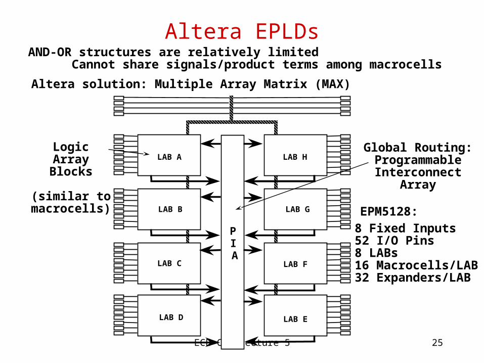
Altera EPLDsAND-OR structures are relatively limited Cannot share signals/product terms among macrocells
Altera solution: Multiple Array Matrix (MAX)
LogicArray
Blocks
(similar tomacrocells)
Global Routing:ProgrammableInterconnect
Array
8 Fixed Inputs52 I/O Pins8 LABs16 Macrocells/LAB32 Expanders/LAB
EPM5128:

ECE C03 Lecture 5 26
Altera EPLDsLAB Architecture
Expander Terms shared among allmacrocells within the LAB
Macrocell ARRAY
I/O Block
Expander Product Term
ARRAY
I NPUTS
P I
A
I/O Pad
I/O Pad
Macrocell P-Terms
Expander P-Terms

ECE C03 Lecture 5 27
Altera EPLDsP22V10 PAL
0 ASYNCHRONOUS RESET (TO ALL REGISTERS)
23AR
88132176220264308352396
44
22
2
OUTPUT LOGIC
MACROCELL
P - 5810 R - 5811
528572616660704748792836
484
880
440
21
3
OUTPUT LOGIC
MACROCELL
P - 5812 R - 5813
10561100114411881232127613201364
1012
1408
924
968
1452
20
4
OUTPUT LOGIC
MACROCELL
P - 5814 R - 5815
16721716176018041848189219361980
1628
2024
1496
1584
2068
1540
2112
19
5
OUTPUT LOGIC
MACROCELL
P - 5816 R - 5817
23762420246425082552259626402684
2332
2728
2156
2288
2772
22442200
28162860
1
1
0
0
1
0
0
1
D Q
QSP
10
5808P
R5809
10 4 8 12 16 20 24 28 32 36 40
INCREMENT
FIRST FUSE NUMBERS
15
9
OUTPUT LOGIC
MACROCELL
P - 5824 R - 5825
49725016506051045148519252365280
4928
5324
4884
17
7
OUTPUT LOGIC
MACROCELL
P - 5820 R - 5821
38283872391639604004404840924136
3784
4180
3652
3740
4224
3696
4268
16
8
OUTPUT LOGIC
MACROCELL
P - 5822 R - 5823
44444488453245764620466447084752
4400
4796
4312
4356
4840
18
6
OUTPUT LOGIC
MACROCELL
P - 5818 R - 5819
31243168321232563300334433883432
3080
3476
2904
3036
3520
29922948
35643608
14
10
OUTPUT LOGIC
MACROCELL
P - 5826 R - 5827
54125456550055445588563256765720
5368
11
5764
13
SYNCHRONOUS PRESET
(TO ALL REGISTERS)
0 4 8 12 16 20 24 28 32 36 40INCREMENT
Supports large number of product terms per outputLatches and muxes associated with output pins

ECE C03 Lecture 5 28
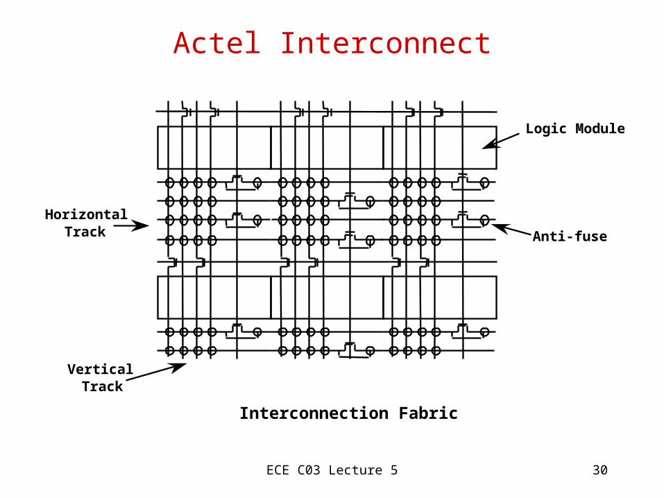
Actel Programmable Gate Arrays
Rows of programmablelogic building blocks
+
rows of interconnect
Anti-fuse Technology:Program Once
8 input, single output combinational logic blocks
FFs constructed from discrete cross coupled gates
Use Anti-fuses to buildup long wiring runs from
short segments
I/O Buffers, Programming and Test Logic
Logic Module Wiring Tracks
I/O Buffers, Programming and Test Logic
I/O
Bu
ffer
s, P
rog
ram
min
g a
nd
Tes
t L
og
ic
I/O B
uffers, P
rog
ramm
ing
and
Test L
og
ic

ECE C03 Lecture 5 29
Actel Logic ModuleBasic Module is aModified 4:1 Multiplexer
Example: Implementation of S-R Latch
2:1 MUXD0
D1
SOA
2:1 MUXD2
D3
SOB
2:1 MUX
S0
Y
S1
2:1 MUX"0"
R
2:1 MUX"1"
S
2:1 MUX Q
"0"
ECE C03 Lecture 5 30
Actel Interconnect
Interconnection Fabric
Logic Module
Horizontal Track
Vertical Track
Anti-fuse

ECE C03 Lecture 5 31
Actel Routing Example
Jogs cross an anti-fuse
minimize the # of jobs for speed critical circuits
2 - 3 hops for most interconnections
Logic Module
Logic ModuleLogic Module Output
Input
Input

ECE C03 Lecture 5 32
Xilinx Logic Cell Arrays
CMOS Static RAM Technology: programmable on the fly!
All personality elements connected into serial shift register
Shift in string of 1's and 0's on power up
General Chip Architecture: • Logic Blocks (CLBs) • IO Blocks (IOBs) • Wiring Channels
IOB IOB IOB IOB
CLB CLB
CLB CLB
IOB
IOB
IOB
IOB
Wiring Channels

ECE C03 Lecture 5 33
Xilinx LCA Architecture
Inputs: Tri-state enable bit to output input, output clocks
Outputs: input bit
Internal FFs for input & output paths
Fast/Slow outputs 5 ns vs. 30 ns rise
Pull-up used with unused IOBs
D Q
OUT INV
TS INV
OUTPUT SOURCE
SLEW RATE
PASSIVE PULLUP
MUX
R
DQ
R
Vcc
PAD
Output Buffer
TTL or CMOS Input Buffer
Global ResetClocks
Enable Output
Out
Direct In
Registered In
Program Controlled Options

ECE C03 Lecture 5 34
Xilinx LCA Architecture
Configurable Logic Block: CLB
2 FFs
Any function of 5 Variables
Global Reset
Clock, Clock Enb
Independent DIN
Combinational Function
Generator
D RDQ
CEMux
D RDQ
CE
Mux
Mux
Mux
Mux
A B C D E
Q1
Q2
Reset
DIN
Clock
Clock Enable
F
G
X
Y

ECE C03 Lecture 5 35
Xilinx CLB Function Generator
CLB Function Generator
Any function of 5 variables
Two Independent Functionsof 4 variables each
Function of 5
Variables
F
G
Mux
Mux
AB
C
DE
Q1
Q2
Function of 4
VariablesF
Mux
Mux
AB
C
DE
Q1
Q2
Mux
Function of 4
VariablesG
Mux
Mux
AB
C
DE
Q1
Q2
Mux

ECE C03 Lecture 5 36
Xilinx CLB Function Generator
Certain LimitedFunctions of 6 Variables
Function of 4
VariablesE
Mux
Mux
AB
C
D
Q1
Q2
Function of 4
Variables
Mux
Mux
AB
C
D
Q1
Q2
Mux
F
G
ECE C03 Lecture 5 37
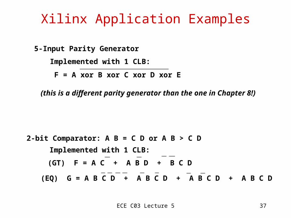
Xilinx Application Examples
5-Input Parity Generator
Implemented with 1 CLB:
F = A xor B xor C xor D xor E
2-bit Comparator: A B = C D or A B > C D
Implemented with 1 CLB:
(GT) F = A C + A B D + B C D
(EQ) G = A B C D + A B C D + A B C D + A B C D
(this is a different parity generator than the one in Chapter 8!)

ECE C03 Lecture 5 38
Xilinx Application Examples
n-Input Majority Circuit
Assert 1 whenever n/2 or greater inputs are 1
n-input Parity Functions 5 input = 1 CLB, 2 Levels of CLBs yield up to 25 inputs!
CLB
5-input Majority Circuit
CLB
CLB
CLB
7-input Majority Circuit
CLB
CLB
9 Input Parity Logic
ECE C03 Lecture 5 39
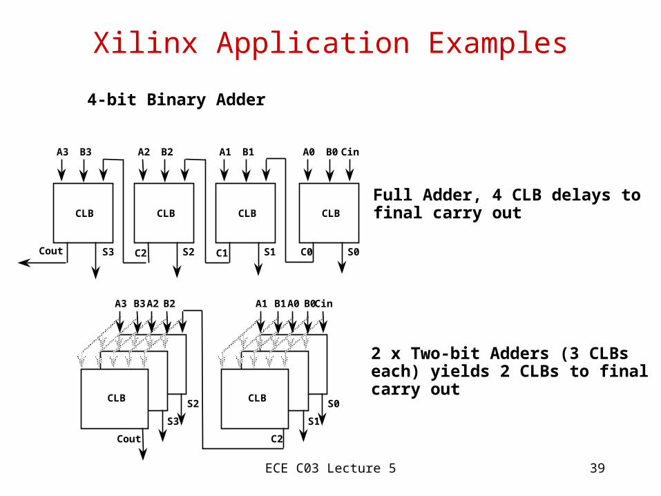
Xilinx Application Examples
4-bit Binary Adder
CLB
A0 B0 Cin
S0
CLB
A1 B1
S1
CLB
A2 B2
C1S2
CLB
A3 B3
C2S3 C0Cout
S0
S1
C2
A1 B1 CinA0 B0
CLBS2
S3
Cout
A3 B3A2 B2
CLB
Full Adder, 4 CLB delays tofinal carry out
2 x Two-bit Adders (3 CLBseach) yields 2 CLBs to finalcarry out

ECE C03 Lecture 5 40
Xilinx Interconnect Architecture
Interconnect
Direct Connections
Global Long Line
Horizontal/Vertical Long Lines
Switching Matrix Connections
X
YCLB3
A
D
DIBCKE R
CE
X
YCLB1
A
D
DIBCKE R
CEX
YCLB0
A
D
DIBCKE R
CE
Direct Connections
Horizontal Long Line
Vertical Long Lines
Global Long Line
Switching Matrix
Horizontal Long Line
X
YCLB2
A
D
DIBCKE R
CE

ECE C03 Lecture 5 41
Comparison of Recent Xilinx Architectures
Parameter XC 4025 XC3195 XC 2018Number of FFs 2560 1320 174
Number of I/Os 256 176 74
Number of logic inputsper CLB
9 5 4
Function generators perCLB
3 2 2
Fast Carry Logic yes no no
Number of logic outputsper CLB
4 2 2
RAM bits 32768 0 0

ECE C03 Lecture 5 42
Summary
• Combinational Logic Implementations• Multiplexers• Decoders• ROMS• Field Programmable Logic Arrays• READING: Katz 4.2.2, 4.2.3, 4.2.4, 4.2.5, 10.3,
Dewey 5.7