3. LECTURE: COMBINATIONAL LOGIC...
33
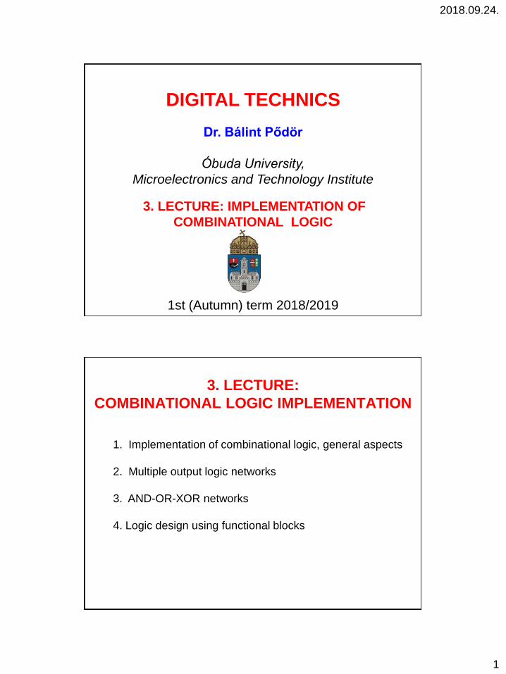
2018.09.24. 1 DIGITAL TECHNICS Dr. Bálint Pődör Óbuda University , Microelectronics and Technology Institute 3. LECTURE: IMPLEMENTATION OF COMBINATIONAL LOGIC 1st (Autumn) term 2018/2019 3. LECTURE: COMBINATIONAL LOGIC IMPLEMENTATION 1. Implementation of combinational logic, general aspects 2. Multiple output logic networks 3. AND-OR-XOR networks 4. Logic design using functional blocks
Transcript of 3. LECTURE: COMBINATIONAL LOGIC...
2018.09.24.
1
DIGITAL TECHNICS
Dr. Bálint Pődör
Óbuda University,
Microelectronics and Technology Institute
3. LECTURE: IMPLEMENTATION OF
COMBINATIONAL LOGIC
1st (Autumn) term 2018/2019
3. LECTURE:
COMBINATIONAL LOGIC IMPLEMENTATION
1. Implementation of combinational logic, general aspects
2. Multiple output logic networks
3. AND-OR-XOR networks
4. Logic design using functional blocks

2018.09.24.
2
SYNTHESIS USING LOGIC GATES
The traditional process of logic synthesis is based on the
application of logic gates.
Its more modern variant makes use of programmable logic
devices too.
However in many case it is more advantageous to use a
logic synthesis procedure based on the application of logic
functional blocks.
IMPLEMENTING COMBINATIONAL LOGIC
The different steps involved in the design of a combinational
logic circuit are as follows:
1. Statement of the problem.
2. Identification of input and output variables.
3. Expressing the relationship between the input and output
variables.
4. Construction of a truth table to meet input–output
requirements.
5. Writing Boolean expressions for various output variables
in terms of input variables.
6. Minimization of Boolean expressions.
7. Implementation of minimized Boolean expressions.

2018.09.24.
3
IMPLEMENTING COMBINATIONAL LOGIC
These different steps are self-explanatory. One or two points,
however, are worth mentioning here.
There are various simplification techniques available for
minimizing Boolean expressions, which have been discussed
in the previously. These include the use of theorems and
identities, Karnaugh mapping, the Quine–McCluskey
tabulation method and so on. Also, there are various possible
minimized forms of Boolean expressions.
The following guidelines should be followed while choosing
the preferred form for hardware implementation:
IMPLEMENTING COMBINATIONAL
LOGIC 1. The implementation should have the minimum number
of gates, with the gates used having the minimum
number of inputs.
2. There should be a minimum number of interconnections,
and the propagation time should be the shortest.
3. Limitation on the driving capability of the gates should
not be ignored.
It is difficult to generalize as to what constitutes an
acceptable simplified Boolean expression. The importance of
each of the above-mentioned aspects is governed by the
nature of application.

2018.09.24.
4
Problem statement
Truth Table
Minimized
PoS form
Elimination of hazards
Impementation:
NAND gates
Sum of minterms form
Minterm table
Product of maxterms form
Maxterm table
Minimized
SoP form
Elimination of hazards
Implementation:
NOR gates
Implementation:
NOT-AND-OR
Flow diagram of logic synthesis procedure using gates
IMPLEMENTATION OPTIONS
Ready-made catalog-order (modular) devices (gates,
functional blocks, etc.)
Custom-design devices
Gate-array devices
Programmable logic devices (PLD), e.g. programmable logic
array (PLA), programmable array logic (PAL), etc.
Table look-up (ROM)
Microcomputer
2018.09.24.
5
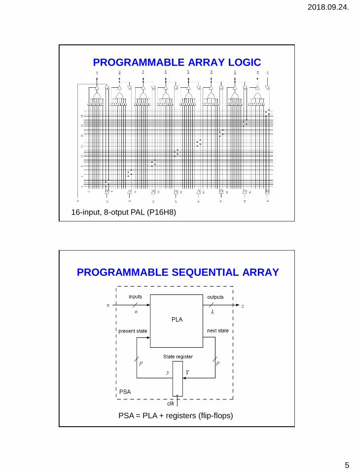
PROGRAMMABLE ARRAY LOGIC
16-input, 8-otput PAL (P16H8)
PROGRAMMABLE SEQUENTIAL ARRAY
PSA = PLA + registers (flip-flops)

2018.09.24.
6
11
EXAMPLE: CODE CONVERTERS WITH ROM
Various codes are used in digital technics. For the solution of
a given task a certain type of code might be the most
appropriate, however for an other different task an other
code type might be more advantageous.
E. g. in a digital position or angle sensor it is advantageous
to use the Gray code. However the treating of measurement
data and performing arithmetics would be rather complicated
in Gray code, for this the binary code is the best choice.
The various BCD type codes play an important role in the
information exchange between the digital systems and
human beings, however inside the system itself the use of
such code is disadvantageous because of memory capacity
usage, and more complicated arithmetics.
For this reason code conversion is a commonly occurring
task in various digital systems.
12
ROM APPLICATIONS: CODE
CONVERSIONS
One important application of ROMs in combinational logic is
the code conversion.
n-bit code m-bit code necessary memory capacity:
m x 2n.
Practical examples:
8-bit binary code 8-bit Gray code: 256x8 ROM.
13-bit binary code 4 tetrad BCD code:
Two 8-kbyte capacity EPROM, 1s, and 10s, and 100s and
1000s respectively, (13 bit: 0-8191).

2018.09.24.
7
CODE CONVERSION USING ROM
A0 D0
… ...
… …
A12 D7
A0 D0
… ...
… …
A12 D7
BCD outputs
1s and 10s
100s and 1000s
Binary inputs
B0 … B12
13-bit binary code to 4 tetrad BCD code converter
14
ROM BASED LOGIC: MULTIPLIER
X Y Z 0*0 00 00 0000 0*1 00 01 0000 0*2 00 10 0000 0*3 00 11 0000 1*1 01 01 0001 1*2 01 10 0010 1*3 01 11 0011 2*0 10 00 0000 2*1 10 01 0010 2*2 10 10 0100 2*3 10 11 0110 3*0 11 00 0000 3*1 11 01 0011 3*2 11 10 0110 3*3 11 11 1001
ROM
16x 4bit
Z
X
Y
Fast, simple, cheap,
Can generate any function
(look-up-table, LUT)
LUT based logic is used in
several types of FPGAs.

2018.09.24.
8
8x8 BIT COMBINATIONAL MULTIPLIER
4x4 bit partial products are generated by four 256x8 bit ROMs
LUT(ROM) BASED SYSTEM LOGIC
BLOCK
In general, a logic block (CLB or LAB) consists of a few
logical cells (called ALM, LE, Slice etc). A typical cell
consists of a 4-input Lookup table (LUT), a Full adder (FA)
and a D-type flip-flop. The LUT are in this figure split into
two 3-input LUTs. In normal mode those are combined into
a 4-input LUT through the left mux.
2018.09.24.
9
17
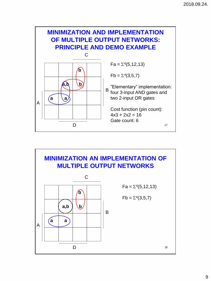
MINIMIZATION AND IMPLEMENTATION
OF MULTIPLE OUTPUT NETWORKS:
PRINCIPLE AND DEMO EXAMPLE
b
a
a,b
a
b
C
B
D
A
Fa = 4(5,12,13)
Fb = 4(3,5,7)
”Elementary” implementation:
four 3-input AND gates and
two 2-input OR gates
Cost function (pin count):
4x3 + 2x2 = 16
Gate count: 6
18
MINIMIZATION AN IMPLEMENTATION OF
MULTIPLE OUTPUT NETWORKS
b
a
a,b
a
b
C
B
D
A
Fa = 4(5,12,13)
Fb = 4(3,5,7)

2018.09.24.
10
MINIMIZATION AN IMPLEMENTATION OF
MULTIPLE OUTPUT NETWORKS
19
& & &
1 1
Fa Fb
_ _ _ _
A B C A B C D A C D
Pin count: 14
Gate count: 5
MINIMIZATION AN IMPLEMENTATION OF
MULTIPLE OUTPUT NETWORKS
In this example the independent minimization of the two
outputs of the pin count is 16, the common minimization
yields 14 pins. The gate counts were 6 and 5 respectively.
The common minimization is generally noticeably optimal, in
this case the pin number decreased by 12.5 percent.
The common implicant can be found by graphical or by
numerical methods. For more then 3 or for outputs the
transparency of the graphical method is strongly reduced, in
such cases e.g. the appropriately modified Quine-McCluskey
algorithm can be used.

2018.09.24.
11
EXAMPLE: MINIMIZATION OF THREE
OUTPUT LOGIC FUNCTION
21
Determine the simplest conceptual two-level AND-OR
logic diagram of the three output logic network:
Fa = 4(0,1,5,6,7,13)
Fb = 4(0,1,5,10-15)
Fc = 4(0,1,8-11,14,15)
The common prime implicants of Fa and Fb are the prime
implicants of the product function Fab = FaFb, etc.
COMMON (PRIME) IMPLICANTS
22
Product functions (pairs):
Fa = 4(0,1,5,6,7,13)
Fb = 4(0,1,5,10-15)
Fc = 4(0,1,8-11,14,15)
Fab = FaFb = 4(0,1,5,13) = m(0,1) + m(5,13)
Fbc = FbFc = 4(0,1,10,11,14,15) = (0,1) + m(10,11,14,15)
Fca = FcFa = 4(0,1) = m(0,1)

2018.09.24.
12
RESULT OF MINIMIZATION (1)
23
Principle: the common prime implicants occurring in more
outputs are implemented only once.
Fa,Fb,Fc: /A /B /C m(0,1)
Fa,Fb: B /C D m(5,13)
Fa,Fb: A C m(10,11,14,15)
24
BCD to 7–segment control signal
decoder
c0 c1 c2 c3 c4 c5 c6
A B C D
ANOTHER EXAMPLE: BCD TO
7-SEGMENT DISPLAY CONTROLLER
• Understanding the problem
– Input is a 4 bit BCD digit (A, B, C, D)
– Output is the control signals for the display (7 outputs
C0 – C6)
• Block diagram c1 c5
c2 c4 c6
c0
c3

2018.09.24.
13
25
A B C D C0 C1 C2 C3 C4 C5 C6
0 0 0 0 1 1 1 1 1 1 0
0 0 0 1 0 1 1 0 0 0 0
0 0 1 0 1 1 0 1 1 0 1
0 0 1 1 1 1 1 1 0 0 1
0 1 0 0 0 1 1 0 0 1 1
0 1 0 1 1 0 1 1 0 1 1
0 1 1 0 1 0 1 1 1 1 1
0 1 1 1 1 1 1 0 0 0 0
1 0 0 0 1 1 1 1 1 1 1
1 0 0 1 1 1 1 0 0 1 1
1 0 1 – – – – – – – –
1 1 – – – – – – – – –
FORMALIZE THE PROBLEM
• Truth table
– Show don't cares
• Choose implementation
target
– If ROM, we are done
– Don't cares imply PAL/PLA
may be attractive
• Follow implementation
procedure
– Minimization using K-maps
26
C0 = A + B D + C + B' D' C1 = C' D' + C D + B' C2 = B + C' + D C3 = B' D' + C D' + B C' D + B' C C4 = B' D' + C D' C5 = A + C' D' + B D' + B C' C6 = A + C D' + B C' + B' C
IMPLEMENTATION AS MINIMIZED
SUM-OF-PRODUCTS (SOP)
• 15 unique product terms when minimized individually
1 0 X 1
0 1 X 1
1 1 X X
1 1 X X
D
A
B
C
1 1 X 1
1 0 X 1
1 1 X X
1 0 X X
D
A
B
C
0 1 X 1
0 1 X 1
1 0 X X
1 1 X X
D
A
B
C
1 1 X 1
1 1 X 1
1 1 X X
0 1 X X
D
A
B
C
1 0 X 1
0 1 X 0
1 0 X X
1 1 X X
D
A
B
C
1 0 X 1
0 0 X 0
0 0 X X
1 1 X X
D
A
B
C
1 1 X 1
0 1 X 1
0 0 X X
0 1 X X
D
A
B
C

2018.09.24.
14
27
C0 = B C' D + C D + B' D' + B C D' + A C1 = B' D + C' D' + C D + B' D' C2 = B' D + B C' D + C' D' + C D + B C D' C3 = B C' D + B' D + B' D' + B C D' C4 = B' D' + B C D' C5 = B C' D + C' D' + A + B C D' C6 = B' C + B C' + B C D' + A
C0 = A + B D + C + B' D' C1 = C' D' + C D + B' C2 = B + C' + D C3 = B' D' + C D' + B C' D + B' C C4 = B' D' + C D' C5 = A + C' D' + B D' + B C' C6 = A + C D' + B C' + B' C
C2
IMPLEMENTATION AS MINIMIZED SOP
(CONT’D)
• Can do better
– 9 unique product terms (instead of 15)
– Share terms among outputs
– Each output not necessarily in minimized form
1 1 X 1
1 1 X 1
1 1 X X
0 1 X X
D
A
B
C
1 1 X 1
1 1 X 1
1 1 X X
0 1 X X
D
A
B
C
C2
28
C0 = B C' D + C D + B' D' + B C D' + A C1 = B' D + C' D' + C D + B' D' C2 = B' D + B C' D + C' D' + C D + B C D' C3 = B C' D + B' D + B' D' + B C D' C4 = B' D' + B C D' C5 = B C' D + C' D' + A + B C D' C6 = B' C + B C' + B C D' + A
C0 = A + B D + C + B' D' C1 = C' D' + C D + B' C2 = B + C' + D C3 = B' D' + C D' + B C' D + B' C C4 = B' D' + C D' C5 = A + C' D' + B D' + B C' C6 = A + C D' + B C' + B' C
C2
IMPLEMENTATION AS MINIMIZED SOP
(CONT’D)
• Can do better
– 9 unique product terms (instead of 15)
– Share terms among outputs
– Each output not necessarily in minimized form
1 1 X 1
1 1 X 1
1 1 X X
0 1 X X
D
A
B
C
1 1 X 1
1 1 X 1
1 1 X X
0 1 X X
D
A
B
C
C2

2018.09.24.
15
29
BC'
B'C
B'D
BC'D
C'D'
CD
B'D'
A
BCD'
A B C D
C0 C1 C2 C3 C4 C5 C6 C7
PLA IMPLEMENTATION
30
AND-OR-XOR LOGIC DEMO EXAMPLE:
BCD-TO-GLIXON CODE CONVERSION
0 1 2 3
7
8
6
9
5 4
C
B
D
A
Design a (normal)
BCD/Glixon code
converter. The illegal code
words cannot be present at
the inputs.

2018.09.24.
16
EXAMPLE (EXCLUSIVE-OR LOGIC):
BCD-TO-GLIXON CODE CONVERTER
31
The Glixon code is a one-step BCD code (the Hamming
distance is 1). The code words from 0 to 9 are
0000(0) 0001(1) 0011(2) 0010(3) 0110(4)
0111(5) 0101(6) 0100(7) 1100(8) 1000(9)
Normal BCD code: ABCD (A is the MSB)
Glixon code: E3, E2, E1, E0 (E3 is the MSB).
E3 = Σ4(8,9)X(10-15)
E2 = Σ4(4-8)X(10-15)
E1 = Σ4(2-5)X(10-15)
E0 = Σ4(1,2,5,6)X(10-15)
MINIMIZED TWO LEVEL AND-OR CIRCUIT
32
&
&
&
&
&
1
1
1
E3 = A
_
E2 = B + A D
_ _
E1 = B C + B C
_ _ _
E0 = C D + A C D
Pin count 18
Gate count 8
(plus 4 inverters at
the inputs

2018.09.24.
17
AND-OR-EXCLUSIVE-OR LOGIC
IMPLEMENTATION
33
Using XOR gates in implementing (partially) symmetric
logic functions make possible to obtain more economical
solutions than using standard optimized two-level AND-
OR or OR-AND circuits.
Here this approach can be applied to E1 and E0.
Full or partial symmetry is evident on the Karnaugh map
by noting the chessboard patterns.
34
AND-OR-XOR LOGIC: E1
1 1
1
X
1
X
X
X
X
X
C
B
D
A
_ _
E1 = B C + B C
(three gates)
E1 = B C
One gate instead of
three!

2018.09.24.
18
35
AND-OR-XOR LOGIC: E0
1 1
X
1
X
1
X
X
X
X
C
B
D
A
_ _ _
E0 = C D + A C D
(three gates)
_
E0 = A (C D)
Two gates instead of
three!
AND-OR-XOR LOGIC IMPLEMENTATION
36
&
=1
=1
1
&
E3 = A
_
E2 = B + A D
E1 = B C
_
E0 = A (C D)
Pin count 11
Gate count 5
Additional benefit: 2 inverters instead of 4 at the input!

2018.09.24.
19
2-LEVEL AND/OR VERSUS AND/OR/XOR
Comparison of the two approaches (including input
inverters where necessary:
two-level AND/OR (three-level) AND/ORXOR
Pin count 18 11
Gate count 8 5
Input inverters 4 2
COMBINATIONAL LOGIC DESIGN
USING FUNCTIONAL BLOCKS
The traditional process of logic synthesis is based on the
application of logic gates.
However in many case it is more advantageous to use a
logic synthesis procedure based on the application of logic
functional blocks.
Demo examples: Functional units (multiplexer, decoder) as building blocks Logical function unit Mux based shifter
2018.09.24.
20
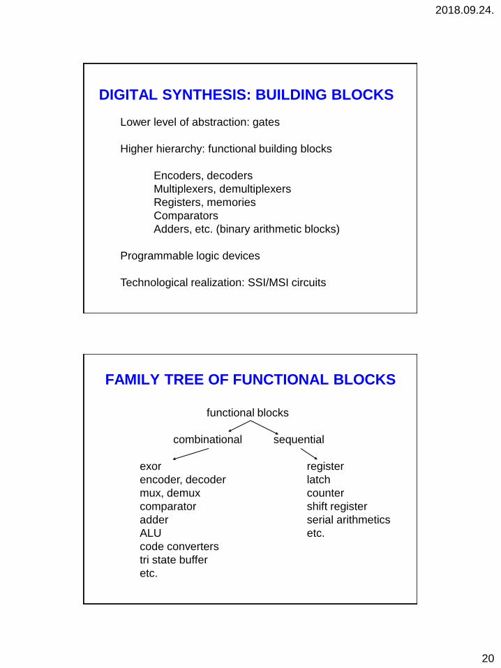
DIGITAL SYNTHESIS: BUILDING BLOCKS
Lower level of abstraction: gates
Higher hierarchy: functional building blocks
Encoders, decoders
Multiplexers, demultiplexers
Registers, memories
Comparators
Adders, etc. (binary arithmetic blocks)
Programmable logic devices
Technological realization: SSI/MSI circuits
FAMILY TREE OF FUNCTIONAL BLOCKS
functional blocks
combinational sequential
exor register
encoder, decoder latch
mux, demux counter
comparator shift register
adder serial arithmetics
ALU etc.
code converters
tri state buffer
etc.

2018.09.24.
21
DIGITAL COMPONENTS
High level digital circuit designs are normally made using collections of
logic gates referred to as components, rather than using individual logic
gates.
Levels of integration (numbers of gates) in an integrated circuit (IC):
Small scale integration (SSI): about 10 gates.
Medium scale integration (MSI): 10 to 100 gates.
Large scale integration (LSI): 100-1,000 logic gates.
Very large scale integration (VLSI): 1,000-upward.
Ultra large scale integration (ULSI): 10,000-upward.
Giga large scale Integration (GLSI): 100, 000 upward.
Ridiculously (?) large scale integration (RLSI): 1,000,000 upward.
These levels are approximate, but the distinctions are useful in
comparing the relative complexity of circuits.
What we need to know about an MSI
circuit? • Function: what it does
• Truth-table: input-output
• Logic gate diagram: how it does it
• Packaging (module pin-out): how to build it
• Dynamic behavior (timing diagram)
• Applications: where to use it
Common MSI circuits:
programmable logic devices (PLDs)
encoder, decoder, exor, comparator, mux, demux, adder, subtractor,
arithmetic circuits (adders, multipliers)
Arithmetic and Logic Unit (ALU)

2018.09.24.
22
• Any combinational circuit can be constructed using decoders and OR gates!
• Example: Implement a full adder circuit with a decoder and two OR gates.
• Recall full adder equations, and let X, Y, and Z be the inputs: – S(X,Y,Z) = X+Y+Z = m(1,2,4,7) – C (X,Y,Z) = m(3, 5, 6, 7).
• Since there are 3 inputs and a total of 8 minterms, we need
a 3-to-8 decoder.
DECODER APPLICATION: IMPLEMENTING
BOOLEAN FUNCTIONS USING DECODERS
IMPLEMENTING A BINARY ADDER
USING A DECODER
S(X,Y,Z) = SUM m(1,2,4,7)
C(X,Y,Z) = SUM m(3,5,6,7)

2018.09.24.
23
MULTIPLEXER AS AN UNIVERSAL
COMBINATIONAL CIRCUIT
From the point of view of output(s) the multiplexer can be
considered as a one level combinational circuit.
Its characteristics is the fast response time.
For the selected input the time delay corresponds to the unit
gate delay.
MULTIPLEXER BASED IMPLEMTATION
OF XOR FUNCTION

2018.09.24.
24
USING A 4-1 MUX TO IMPLEMENT THE
MAJORITY FUNCTION
Principle: Use the A and B inputs to select a pair of minterms.
The value applied to the MUX input is
selected from {0, 1, C, C’} to pick the desired behaviour of the
minterm pair.
EXAMPLE: USING MULTIPLEXER TO
IMPLEMENT AN ADDER
Rearrange truth table:
Use Ai, Bi to select MUX output, connect Ci and Ci’ to MUX
data inputs.
Implement with two 4-to-1 multiplexers and one inverter (to
generate Ci’)
Ai Bi Si Ci+1
0 0 Ci 0
_
0 1 Ci Ci
_
1 0 Ci Ci
1 0 Ci 1

2018.09.24.
25
1-BIT FULL ADDER:
MUX IMPLEMENTATION
49
74153 dual 4-line to 1-line data selector/multiplexer.
Two 4/2/1 multiplexers in one package.
An inverter is also necessary (e.g. 1/6 7404 hex inverter).
C0 C1 C2 Function Comments 0 0 0 1 always 1 0 0 1 A + B logical OR 0 1 0 (A • B)' logical NAND 0 1 1 A XOR B logical XOR 1 0 0 A XNOR B logical XNOR 1 0 1 A • B logical AND 1 1 0 (A + B)' logical NOR 1 1 1 0 always 0
3 control inputs: C0, C1, C2 2 data inputs: A, B 1 output: F
EXAMPE:
MULTI PURPOSE FUNCTION BLOCK •Multi-purpose Function Block
– 3 control inputs to specify operation to perform on
operands
– 2 data inputs for operands
– 1 output of the same bit-width as operands

2018.09.24.
26
IMPLEMENTATION WITH LOGIC GATES C0 C1 C2 A B F 0 0 0 0 0 1 0 0 0 0 1 1 0 0 0 1 0 1 0 0 0 1 1 1 0 0 1 0 0 0 0 0 1 0 1 1 0 0 1 1 0 1 0 0 1 1 1 1 0 1 0 0 0 1 0 1 0 0 1 1 0 1 0 1 0 1 0 1 0 1 1 0 0 1 1 0 0 0 0 1 1 0 1 1 0 1 1 1 0 1 0 1 1 1 1 0 1 0 0 0 0 1 1 0 0 0 1 0 1 0 0 1 0 0 1 0 0 1 1 1 1 0 1 0 0 0 1 0 1 0 1 0 1 0 1 1 0 0 1 0 1 1 1 1 1 1 0 0 0 1 1 1 0 0 1 0 1 1 0 1 0 0 1 1 0 1 1 0 1 1 1 0 0 0 1 1 1 0 1 0 1 1 1 1 0 0 1 1 1 1 1 0
F = 5(0-3,5-10,13,14,16,19,23,24)
Minimization on 5 variable
Karnaugh map:
four 4-cubes
0
1
2
3
5
6
7
8
9
10
13
14
16
19
23
24
1
0
A B
A B
A B
FORMALIZE THE PROBLEM
C0 C1 C2 A B F 0 0 0 0 0 1 0 0 0 0 1 1 0 0 0 1 0 1 0 0 0 1 1 1 0 0 1 0 0 0 0 0 1 0 1 1 0 0 1 1 0 1 0 0 1 1 1 1 0 1 0 0 0 1 0 1 0 0 1 1 0 1 0 1 0 1 0 1 0 1 1 0 0 1 1 0 0 0 0 1 1 0 1 1 0 1 1 1 0 1 0 1 1 1 1 0 1 0 0 0 0 1 1 0 0 0 1 0 1 0 0 1 0 0 1 0 0 1 1 1 1 0 1 0 0 0 1 0 1 0 1 0 1 0 1 1 0 0 1 0 1 1 1 1 1 1 0 0 0 1 1 1 0 0 1 0 1 1 0 1 0 0 1 1 0 1 1 0 1 1 1 0 0 0 1 1 1 0 1 0 1 1 1 1 0 0 1 1 1 1 1 0
C2 C0 C1
0
1
2
3
4
5
6
7 S2
8:1 MUX
S1 S0
F
choose implementation technology
5-variable K-map to discrete gates
multiplexer implementation
the target operations are pair wise
inverse of each other
2018.09.24.
27
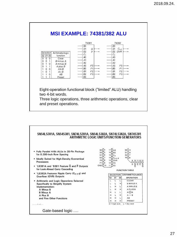
MSI EXAMPLE: 74381/382 ALU
Eight-operation functional block (”limited” ALU) handling
two 4-bit words.
Three logic operations, three arithmetic operations, clear
and preset operations.
Gate-based logic ….

2018.09.24.
28
MUX BASED FUNCTIONAL (SUB-)UNITS
Data shifters and data rotators
Various logic functional units
Combinational adders/subtractors
Arithmetic logic unit (ALU)
Etc.
2018.09.24.
29
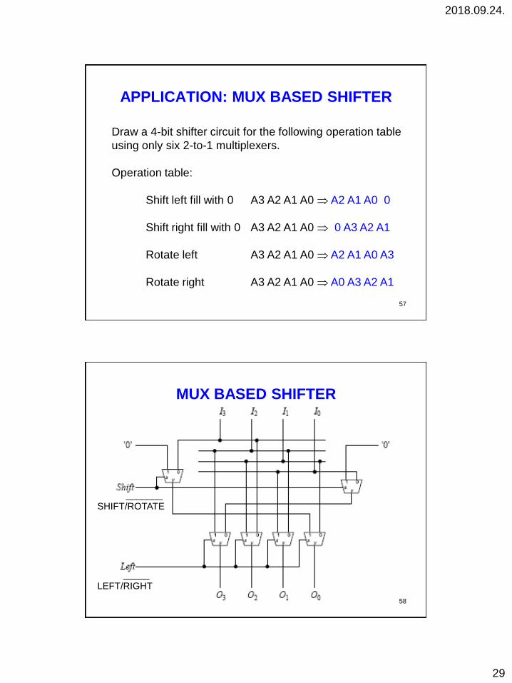
APPLICATION: MUX BASED SHIFTER
57
Draw a 4-bit shifter circuit for the following operation table
using only six 2-to-1 multiplexers.
Operation table:
Shift left fill with 0 A3 A2 A1 A0 A2 A1 A0 0
Shift right fill with 0 A3 A2 A1 A0 0 A3 A2 A1
Rotate left A3 A2 A1 A0 A2 A1 A0 A3
Rotate right A3 A2 A1 A0 A0 A3 A2 A1
MUX BASED SHIFTER
58
_______
SHIFT/ROTATE
_____
LEFT/RIGHT

2018.09.24.
30
59
4-BIT LOGIC FUNCTION (AND, XOR)
CIRCUIT
x3 y3 x2 y2 x1 y1 x0 y0
MUX
MUX
MUX
MUX
z3
z2
z1
z0
s
60
4-BIT ADDER/SUBTRACTOR CIRCUIT
x3 x2 x1 x0
y3
y2
y1
y0
MUX
MUX
MUX
MUX
s
cout
z3 z2 z1 z0
A
B
C
4-bit full adder
cin

2018.09.24.
31
61
4-BIT 4-OPERATION ALU
arithmetic unit
(+/-)
logic unit
(AND/XOR)
x
y
s0
s1
4x 2 input
multiplexer z
4
4
4
4
4
4
4
REVISION QUESTIONS
1. What is a multiplexer circuit? Briefly describe one or two
applications of a multiplexer?
2. Is it possible to enhance the capability of an available
multiplexer in terms of the number of input lines it can handle
by using more than one device? If yes, briefly describe the
procedure to do so, with the help of an example.
3. What is an encoder? How does a priority encoder differ
from a conventional encoder? With the help of a truth table,
briefly describe the functioning of a 10-line to four-line priority
encoder with active LOW inputs and outputs and priority
assigned to the higher-order inputs.
.

2018.09.24.
32
REVISION QUESTIONS
4. What is a demultiplexer and how does it differ from a
decoder? Can a decoder be used as a demultiplexer? If yes,
from where do we get the required input line?
5. Briefly describe how we can use a decoder optimally to
implement a given Boolean function? Illustrate your answer
with the help of an example.
6. What is a look-up table (LUT)? How can it be used to
implement a combinational logic function?
7. Present the layout of the two’s complement
adder/substractor and explain its operation.
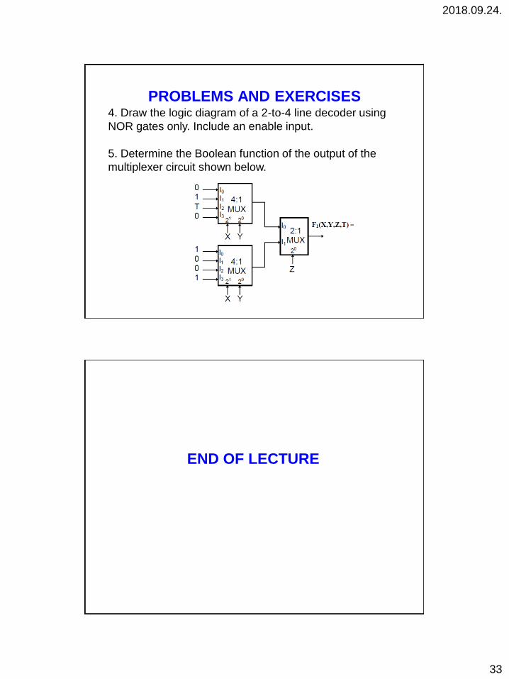
PROBLEMS AND EXERCISES
1. Design, using only multiplexers (and inverters if
necessary), a programmable logic gate, which depending on
the logic value of the control line S, realizes either a two-
input EXCLUSIVE-OR function, or a two-input NAND
function.
2. Implement the 1-bit full subtractor using 4-to-1
multiplexeres.
3. A 4-to-1 multiplexer has signals A and B connected to the
selection inputs S1 and S0, respectively. The data inputs I0
through I3, are as follows: I1 = 0, I2 = 1, I0 = C; and I3 = C’
(C-bar). Determine the Boolean function F(A,B,C) that the
multiplexer implements.
2018.09.24.
33
PROBLEMS AND EXERCISES 4. Draw the logic diagram of a 2-to-4 line decoder using
NOR gates only. Include an enable input.
5. Determine the Boolean function of the output of the
multiplexer circuit shown below.
END OF LECTURE