
Lecture 2 Introduction to...
50
Introduction to Microcontrollers Lecture 2 1
Transcript of Lecture 2 Introduction to...
Introduction to Microcontrollers
Lecture 2
1

Microcontroller
CPU + ++++++++++
Microprocessor
CPU (on single chip)
Microcontrollers
2

What is a Microcontroller Integrated chip that typically contains integrated CPU, memory (RAM
ROM), I/O ports on a single Chip.
System on a single Chip/ small computer on a single chip.
Designed to execute a specific task to control a single system.
Differs from Microprocessor
general-purpose chip
Used to design multi purpose computers or devices
Require Multiple chips to handle various tasks
Typically Microcontroller embedded inside some device.
Microcontrollers are important part of Embedded systems.
Abbreviated µC, uC or MCU.
3

4
Microcontroller Families
68H12: Motorola 68H11, 68HC12, …
8051: Intel 8051, 8052, 80251,…
PIC: Microchip PIC16F628, 18F452, 16F877, …
AVR: Atmel ATmega128, ATtiny28L, AT90S8515,…
We are going to look at AVR

AVR Microcontroller
AVR architecture was conceived by two students(Alf
Egil Bogen & Vegard Wollan RISC ) at Norwegian
Institute of Technology (NTH) and further refined and
developed at Atmel Norway (Atmel AVR).
Atmel says that the name AVR is not an acronym anddoes not stand for anything in particular. The creators ofthe AVR give no definitive answer as to what the term"AVR" stands for. However, it is commonly accepted thatAVR stands for Alf (Egil Bogen) and Vegard (Wollan)'sRisc processor"
5

AVR Microcontroller
AVR Microcontrollers is Family of RISC
Microcontrollers from Atmel.
There are multiple architectures
RISC (Reduced Instruction Set Computer)
CISC (Complex Instruction Set Computer)
6

7
RISC versus CISC
CISC RISC
Emphasis on hardware Emphasis on software
Include multi-clock complex instructions Include single-clock reduce instruction only
Memory-to-memory: “Load” and “Store” incorporated in instructions
Register-to-register: “Load” and “Store” are independent instructions
Small code sizes, high cycles per second Low cycles per second, large code sizes
Transistors used for storing complex instructions
Spends more transistors on memory registers
Most PC's use CPU based on CISC architecture. For instance
Intel and AMD CPU's are based on CISC architectures.
Apple is based on RISC architecture.

The AVR is a Harvard architecture CPU.
Harvard Architecture
Computer architectures that used physically separate storage and signal pathways for their instructions and data.
CPU can read both an instruction and data from memory at the same time that makes it faster.
von Neumann architecture
CPU can Read an instruction or data from/to the memory.
Read, Write can`t occur at the same time due to same memory and signal pathway for data and instructions.
AVR Microcontroller
8

Harvard Architecture
AVR Microcontroller
Harvard Architecture diagram
9

AVR Microcontroller
AVR is a family of 8-bit microntrollers with a large range of variants
differing in:
- Size of program-memory [ Flash]
- Size of EEPROM memory [store long-term information.]
- Size of SRAM [variables]
- Number of I/O pins
- Number of on-chip features such as UART and ADC
Smallest microcontroller is the ATTiny11
Large such as the ATMEGA328
10

AVRs are generally classified into six broad groups:
tinyAVR : the ATtiny series (ATtinyXX) 0.5–8 kB program memory 6–32-pin package Limited peripheral set
megaAVR the ATmega series (ATmegaXXX) 28–100-pin package, 16kB - 128 kB program memory Extended instruction set (Multiply instructions and instructions for handling larger program memories) Extensive peripheral set
XMEGA the ATxmega series 16–384 kB program memory 44–64–100-pin package Extended performance features, such as DMA. Extensive peripheral set with DACs
AVR Basic Families

Application-specific AVRmegaAVRs with special features not found on the othermembers of the AVR family, such as LCD controller, USB
controller, advanced PWM, CAN (controller area network)
AVR with FPGAFPGA 5K to 40K gatesSRAM for the AVR program code, unlike all other AVRsAVR core can run at up to 50 MHz
32-bit AVRsMain article: AVR32In 2006 Atmel released microcontrollers based on the new, 32-
bit, AVR32 architecture. They include SIMD (Singleinstruction, multiple data, is a class of parallelcomputers) and DSP instructions, along with other audio and
video processing features. This 32-bit family of devices isintended to compete with the ARM based processors. Theinstruction set is similar to other RISC cores, but is notcompatible with the original AVR or any of the various ARMcores.
AVR Basic Families

13
AVR Part Numbers
ATmega168
Atmel groupFlash =16KB
ATmega168: 8-bit AVR Microcontroller, 16KB Flash, 28/32-pinATmega328: 8-bit AVR Microcontroller, 32KB Flash, 28/32-pinATmega2560: 8-bit AVR Microcontroller, 256KB Flash, 100-pin

ATmega328 Internal Architecture
14
8-bit CPU
Timer/Counter
Internal memories
32KB Flash
1KB EEPROM
2KB SRAM
Serial Peripheral InterfaceUniversal Synchronous
and Asynchronous serial Receiver and Transmitter (Serial)
GPIO 2-wire Serial Interface

AVR Architecture
15

AVR Architecture1.Registers
Two types of registers
General purpose & Special purpose registers
General purpose registers
32 general purpose registers
Having storage capacity of 8-Bits
Named as R0 to R31.
Can store both Data & Addresses.
Special purpose I/O registers : Three
Program counter (PC)
Stack Pointer (SP)
Status Register (SREG)
*Other I/O registers called SFRs 16

ATmegaxx8 Core Architecture
17

18
General Purpose Registers
• There are 32 8-bit GPR R0-R31– Used as accumulators – for most
math and logic
• X, Y, Z are 16-bit registers that overlap R26-R31– Used as address pointers
– Or to contain larger values (>255)
AVR Register File

Status Register (SREG)
Contains information about the result of the most
recently executed arithmetic instruction.
Information can be used for altering program flow
in order to perform conditional operations.
Updated after any of ALU operations by hardware.
19

(SREG)
20
Bit 7 – I: Global Interrupt Enable
Used to enable and disable interrupts, 1: enabled. 0: disabled.
The I-bit is cleared by hardware after an interrupt has occurred, and is set by the
RETI instruction to enable subsequent interrupts.
Bit 6 – T: Bit Copy Storage
The Bit Copy instructions; BLD (Bit LoaD) and BST (Bit STore) use the T-bit as
source or destination for the operated bit. A bit from a register in the Register File
(GPR) can be copied into T by the BST instruction, and a bit in T can be copied
into a bit in a register in the Register File by the BLD instruction.
Bit 5 – H: Half Carry Flag
The Half Carry Flag H indicates a Half Carry (carry from bit 4) in some arithmetic
operations.
Half Carry is useful in BCD arithmetic.
Bit 4 – S: Sign Bit
Exclusive OR between the Negative Flag N and the Two’s Complement Overflow
Flag V ( S = N ⊕V).

(SREG)
21
Bit 3 – V: Two’s Complement Overflow Flag
The Two’s Complement Overflow Flag V supports two’s complement arithmetic.
Bit 2 – N: Negative Flag
N is the most significant bit of the result.
Bit 1 – Z: Zero Flag
Z indicates a zero result in an arithmetic or logic operation. 1: zero. 0: Non-zero.
Bit 0 – C: Carry Flag
Set if there was carry from the MSB of the result; cleared otherwise.

Program Counter Register(PC)
Holds address of next program instruction tobe executed.
Automatically incremented when the ALUexecutes an instruction.
The size (width) of the program counter of amicrocontroller is measured in bits and isdirectly related to the size of themicrocontroller's program memory(16-bits).
22

Stack Pointer (SP)
In AVR, a stack is implemented as a block of
consecutive bytes in the SRAM memory.
The Stack is mainly used for storing
temporary data, for storing local variables and
for storing return addresses after interrupts
and subroutine calls.
The Stack Pointer Register (16-bits) stores a
pointer to a group of data known at the stack
and always points to the top of the Stack.23
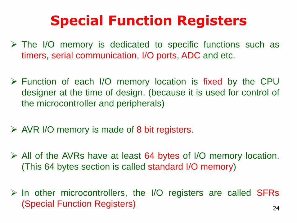
Special Function Registers
24
The I/O memory is dedicated to specific functions such as
timers, serial communication, I/O ports, ADC and etc.
Function of each I/O memory location is fixed by the CPU
designer at the time of design. (because it is used for control of
the microcontroller and peripherals)
AVR I/O memory is made of 8 bit registers.
All of the AVRs have at least 64 bytes of I/O memory location.
(This 64 bytes section is called standard I/O memory)
In other microcontrollers, the I/O registers are called SFRs
(Special Function Registers)

25
NameAddressI/O Mem.
$00 $20 TWBR
$01 $21 TWSR
$04 $24 ADCL
$05 $25 ADCH
$02 $22 TWAR
$03 $23 TWDR
$06 $26 ADCSRA
$07 $27 ADMUX
$08 $28 ACSR
$09 $29 UBRRL
$0A $2A UCSRB
$0B $2B UCSRA
$0C $2C UDR
$0D $2D SPCR
$0E $2E SPSR
$0F $2F
PIND$10 $30
DDRD$11 $31
PORTD$12 $32
PINC$13 $33
DDRC$14 $34
PORTC$15 $35
PINB$16 $36
DDRB$17 $37
PORTB$18 $38
PINA$19 $39
DDRA$1A $3A
PORTA$1B $3B
EECR$1C $3C
EEDR$1D $3D
EEARL$1E $3E
EEARH$1F $3F
SPDR
NameAddressI/O Mem.
NameAddressI/O Mem.
UBRRC$20 $40
UBRRH
$21 $41 WDTCR
$22 $42 ASSR
$23 $43 OCR2
$24 $44 TCNT2
$25 $45 TCCR2
$26 $46 ICR1L
$27 $47 ICR1H
$28 $48 OCR1BL
$29 $49 OCR1BH
OCR1AH$2B $4B
SFIOR$30 $50
OCDR$31 $51
OSCCAL
$32 $52
TCCR0$33 $53
MCUCSR$34 $54
MCUCR$35 $55
TWCR$36 $56
SPMCR$37 $57
TIFR$38 $58
TIMSK$39 $59
TCNT1L$2C $4C
TCNT1H$2D $4D
TCCR1B$2E $4E
TCCR1A$2F $4F
TCNT0
$3A $5A
GICR$3B $5B
OCR0$3C $5C
SPL$3D $5D
SPH$3E $5E
GIFR
OCR1AL$2A $4A SREG$3E $5E
Special Function Registers

I/O Memory Registers
• SREG: Status Register
• SP: Stack Pointer Register
• GIMSK: General Interrupt Mask Register
• GIFR: General Interrupt Flag Register
• MCUCR: MCU General Control Register
• MCUSR: MCU Status Register
• TCNTO: Timer/Counter 0 Register
• TCCR0A: Timer/Counter 0 Control Register A
• TCCR0B: Timer/Counter 0 Control Register B
• OCR0A: Timer/Counter 0 Output Compare Register A
• OCR0B: Timer/Counter 0 Output Compare Register B
• TIMSK0: Timer/Counter 0 Interrupt Mask Register
• TIFR0: Timer/Counter 0 Interrupt Flag Register
• EEAR: EEPROM Address Register
• EEDR: EEPROM Data Register
• EECR: EEPROM Control Register
• PORTB: PortB Data Register
• DDRB: PortB Data Direction Register
• PINB: Input Pins on PortB
• PORTD: PortD Data Register
• DDRD: PortD Data Direction Register
• PIND: Input Pins on PortD
• SPI I/O Data Register
• SPI Status Register
• SPI Control Register
• UART I/O Data Register
• UART Status Register
• UART Control Register
• UART Baud Rate Register
• ACSR: Analog Comparator Control and Status Register

2. AVR Memory
Three parts, each has its own address space:
Data memory Storing data to be processed.
Program memory (flash) Storing program and
sometimes constants.
EEPROM memoryLarge permanent data storage.

Data Memory Space
28

Data Memory (RAM)
General purpose registers.
I/O registers (SFRs).
Internal data SRAM.
External data SRAM
29
In many AVR microcontrollers RAM is split into 4 subsections:

Internal SRAM
30
Internal data SRAM is widely used for storing data andparameters temporary by AVR programmers and Ccompilers.
Each location of the SRAM can be accessed directly by itsaddress.
Each location is 8 bit wide and can be used to store anydata we want.
Size of SRAM is vary from chip to chip, even amongmembers of the same family, ATmega328 has 2KB SRAM.
.Memory is lost when power is shut off (volatile).
Fast read and write.

Data Memory (EEPROM)
31
8-bit EEPROM memory.
ATmega328 contains 1024 bytes.
Different chip have different size of
EEPROM.
Typically reserved for variables that
must retain their value in the event of
a shutdown (non-volatile) (e.g., system
calibration data unique to each board).
Fast read; slow write. Can write individual bytes.
Can be accessed using load and store
instructions with special control bit
settings

Program Memory (flash)
32
16 bit Flash Memory Used to store program code.
Memory contents retained when power is off (non-volatile).
Size dependent on AVR microcontroller
Read-only memory (writing is external to code).
Can only write entire “blocks” of memory at a time.
Fast to read; slow to write.
ATmegaxx8, there are 32KB of program memory (Flash memory)
Organized as 16K 2-byte words
Because program instructions are either 2(common) or 4 (less common) bytes long
Each word (not byte) in Flash memory has a unique address
Beginning address $0000
Ending address $3FFF
Some Flash memory is reserved or protected.
First 42 words (reserved)
bootloader sizes differs from 0.5 to 8 KB for different boards.
$3C00
Reset and interrupt vector section
42 words (84 bytes)
$002A
Your programs go here!
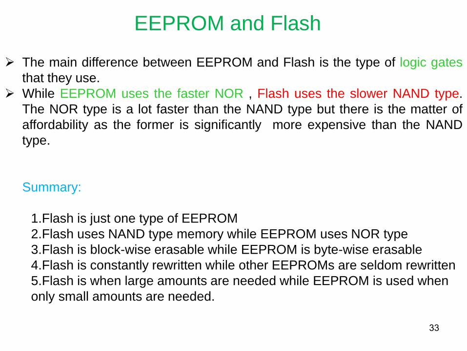
33
The main difference between EEPROM and Flash is the type of logic gates
that they use.
While EEPROM uses the faster NOR , Flash uses the slower NAND type.
The NOR type is a lot faster than the NAND type but there is the matter of
affordability as the former is significantly more expensive than the NAND
type.
Summary:
1.Flash is just one type of EEPROM
2.Flash uses NAND type memory while EEPROM uses NOR type
3.Flash is block-wise erasable while EEPROM is byte-wise erasable
4.Flash is constantly rewritten while other EEPROMs are seldom rewritten
5.Flash is when large amounts are needed while EEPROM is used when
only small amounts are needed.
EEPROM and Flash

Programming AVR Write your program (AVR Studio)
Debug in Simulator mode
Create .hex code
Transfer code to Chip
Connect USB Programmer (AVRISP MKII) to computer and breadboard
Use AVR Studio to download program
AVR Studio: Integrated Development Environment(IDE) for writing and debugging AVR applications forwindows environments.
Place chip in final position and run

What is a Development Board
A printed circuit boarddesigned to facilitatework with a particularmicrocontroller.
• Typical components included in development board:• power circuit • programming interface• basic input; usually buttons and LEDs• I/O pins
35

The Arduino Development Board
36
Arduino (The name is an Italian , meaning “strong friend”) is an open-
source platform used for building electronics projects. Arduino consists of both a
physical programmable circuit board (often referred to as a microcontroller) and a
piece of software, or IDE (Integrated Development Environment) that runs on your
computer, used to write and upload computer code to the physical board.

Arduino Microcontroller Boards
Microcontroller ATmega328
Operating Voltage 5 V
Input Voltage
(recommended)7-12 V
Input Voltage (limits) 6-20 V
Digital I/O Pins 14 (of which 6 provide PWM output)
Analog Input Pins 6
DC Current per I/O Pin 40 mA
DC Current for 3.3V Pin 50 mA
Flash Memory32 KB (ATmega328) of which 2 KB used by
bootloader
SRAM 2 KB (ATmega328)
EEPROM 1 KB (ATmega328)
Clock Speed 16 MHz
37

ATmega328 Internal Architecture
38

ATmega328 Microcontroller
Pin numberPin name
Special function
39

Pins and Ports Overview GND: Ground (0V) VCC: Digital Supply Voltage (2,7 – 5,5V) AVCC: In Arduino Uno and ArduinoMega2560, this pin was simply connected
to VCC. According to the atmel datasheet, this pin should beconnected to a Low-Pass filter when the ADC converted is used.
AREF: Analog Reference Voltage, usually VCC. /Reset: Low level on this pin will generate a reset
Port B, Port C, Port D:
• The communication channels through which information flows into or
out of the microcontroller.
• General Purpose 8 Bit bidirectional I/O Ports, optional internal pullup-
resistors when configured as input, output source capability 20mA.
Special Functions of the Ports available as configured using the SFRs:
Port D: UART, External Interrupts, Analog Comparator. [8 bits]Port B: External Oscillator/Crystal, SPI. [8 bits]Port C: A/D converters, TWI. [7 bits]

Pins and Ports Overview All the work of MCU happens through registers
(special memory locations).
Each port controlled by 3 8-bit registers.
Each bit controls one I/O pin. DDRx: Direction register, defines whether a pin is an input (0)
or and output (1), x denotes the port. DDRB = 0x02; /* sets the
second lowest of port B to output”.
PINx: Pin input value, reading this register returns value of pin.
unsigned int x= PINB; /* Places the status of port B into variable
x */.
PORTx: Pin output value, writing this register sets value of pin.
PORTB = 0x02; /* sets the second bit of port B and clears the
others */ 41

Port Registers
PORTB: PortB Data Register
DDRB: PortB Data Direction Register
PINB: Input Pins on PortB
Bit 7 6 5 4 3 2 1 0
Bit 7 6 5 4 3 2 1 0
Bit 7 6 5 4 3 2 1 0
Similar for Ports C and D.

Arduino Pin Mapping
43

ATmega168/328-Arduino Pin Mapping
44

Arduino Digital and Analog I/O Pins
Digital pins:
• Pins 0 – 7: PORT D [0:7]
• Pins 8 – 13: PORT B [0:5], 6&7 XTAL
• Digital pins 0 and 1 are RX and TX for
serial communication.
• Digital pin 13 connected to the base
board LED.
Analog pins:
• Arduino analog pins (0 – 5) : PORT C
[0:5] , 6 reset 45

Arduino Digital Pin I/O Functions
46
pinMode(pin, mode); Sets pin to INPUT or OUTPUT mode. Writes 1 bit in the DDRx register.
digitalWrite(pin, value); Sets pin value to LOW or HIGH (0 or 1). Writes 1 bit in the PORTx register.
int value = digitalRead(pin); Reads back pin value (0 or 1). Read 1 bit in the PINx register.

Arduino Analog Pin I/O Functions
Analog input pins: 0 – 5 .
Analog output pins: 3, 5, 6, 9, 10, 11 (digital pins) .
Analog input function:
• int val = analogRead(pin), converts (0-5)voltage to a 10-bit number (0 – 1023), don’tuse pinMode, Pin=A0, or Ax.
Analog output function:
• analogWrite(pin, value), value is (0-255),Generates a PWM output on digital pin (3, 5,6, 9, 10, 11) @490Hz frequency, usepinMode(pin, OUTPUT); 47

Example/ Drive LED
48
int myPin = 5; // Arduino digital pin 5
void setup()
{
pinMode(myPin,OUTPUT);
}
void loop()
{
digitalWrite(myPin,HIGH);
delay(1000); //ms
digitalWrite(myPin,LOW);
delay(1000 ); //ms
}
Arduino approach Alternate approach
void setup()
{
DDRD = DDRD | B00100000; // D5
}
void loop()
{
PORTD = PORTD | B00100000;
delay(1000);
PORTD = PORTD & B11011111;
delay(1000);
}

Problem with SRAM size
For example: string
char message[] = "I support the Cape
Wind project.";
Which equals to 33 bytes into SRAM (each
character takes a byte, plus the '\0'
terminator).
If you run out of SRAM, your program
may fail in unexpected ways.
49

To solve this problem
If your sketch talks to a program running on a
(desktop/laptop) computer, you can try shifting
data or calculations to the computer, reducing the
load on the Arduino.
If you have lookup tables or other large arrays,
use the smallest data type necessary to store the
values you need; for example, an int takes up two
bytes, while a byte uses only one (but can store a
smaller range of values).
If you don't need to modify the strings or data
while your sketch is running, you can store them
in flash (program) memory instead of SRAM50


![AVR - dl.melec.irdl.melec.ir/download/pdf/AVR/CodeVision-Fusebit[Melec.ir].pdf · AVR AVR AVR AVR 01 CodeVision CKSEL3..0 Device Clocking Option CKSEL3..0 External Crystal/Ceramic](https://static.fdocuments.us/doc/165x107/5cf6e10d88c99387248bfc0e/avr-dlmelecirdlmelecirdownloadpdfavrcodevision-fusebitmelecirpdf.jpg)