LAYER-MODE TRANSPARENT BOUNDARY … TRANSPARENT BOUNDARY CONDITION FOR THE HYBRID ... TM cases which...
21
Progress In Electromagnetics Research, PIER 94, 175–195, 2009 LAYER-MODE TRANSPARENT BOUNDARY CONDITION FOR THE HYBRID FD-FD METHOD H.-W. Chang, W.-C. Cheng, and S.-M. Lu Institute of Electro-optical Engineering and Department of Photonics National Sun Yat-sen University Kaohsiung 80424, Taiwan Abstract—We combine the analytic eigen mode expansion method with the finite-difference, frequency-domain (FD-FD) method to study two-dimensional (2-D) optical waveguide devices for both TE and TM polarizations. For this we develop a layer-mode based transparent boundary condition (LM-TBC) to assist launching of an arbitrary incident wave field and to direct the reflected and the transmitted scattered wave fields back and forward to the analytical regions. LM- TBC is capable of transmitting all modes including guiding modes, cladding modes and even evanescent waves leaving the FD domain. Both TE and TM results are compared and verified with exact free space Green’s function and a semi-analytical solution. 1. INTRODUCTION Passive dielectric waveguides devices are important building blocks in modern optical communication systems [1, 2]. For 2-D dielectric waveguide problems are divided into mutually independent TE and TM cases which can be solved as scalar wave problems [3,4]. For complex optical devices, full wave methods such as the finite-difference time-domain methods (FD-TD) [5–7] are often used. For very large adiabatic waveguide devices the beam propagation method (BPM) and its variations [8] are used for studying field evolutions and for mode profile determination. BPMs apply a one-way approximation to the Maxwell’s equations making it possible to advance the field solutions plane by plane along the propagation axis. This tremendous saving in computational resources makes BPM the only available option for modeling large complex 3D waveguide devices. Corresponding author: H.-W. Chang ([email protected]).
Transcript of LAYER-MODE TRANSPARENT BOUNDARY … TRANSPARENT BOUNDARY CONDITION FOR THE HYBRID ... TM cases which...

Progress In Electromagnetics Research, PIER 94, 175–195, 2009
LAYER-MODE TRANSPARENT BOUNDARYCONDITION FOR THE HYBRID FD-FD METHOD
H.-W. Chang, W.-C. Cheng, and S.-M. Lu
Institute of Electro-optical Engineering and Department of PhotonicsNational Sun Yat-sen UniversityKaohsiung 80424, Taiwan
Abstract—We combine the analytic eigen mode expansion methodwith the finite-difference, frequency-domain (FD-FD) method to studytwo-dimensional (2-D) optical waveguide devices for both TE and TMpolarizations. For this we develop a layer-mode based transparentboundary condition (LM-TBC) to assist launching of an arbitraryincident wave field and to direct the reflected and the transmittedscattered wave fields back and forward to the analytical regions. LM-TBC is capable of transmitting all modes including guiding modes,cladding modes and even evanescent waves leaving the FD domain.Both TE and TM results are compared and verified with exact freespace Green’s function and a semi-analytical solution.
1. INTRODUCTION
Passive dielectric waveguides devices are important building blocksin modern optical communication systems [1, 2]. For 2-D dielectricwaveguide problems are divided into mutually independent TE andTM cases which can be solved as scalar wave problems [3, 4]. Forcomplex optical devices, full wave methods such as the finite-differencetime-domain methods (FD-TD) [5–7] are often used. For very largeadiabatic waveguide devices the beam propagation method (BPM) andits variations [8] are used for studying field evolutions and for modeprofile determination. BPMs apply a one-way approximation to theMaxwell’s equations making it possible to advance the field solutionsplane by plane along the propagation axis. This tremendous savingin computational resources makes BPM the only available option formodeling large complex 3D waveguide devices.
Corresponding author: H.-W. Chang ([email protected]).

176 Chang, Cheng, and Lu
In 1966 Professor Yee published his now famous 3D FD-TDalgorithm [9]. It was until 1975 when workstations became popularand powerful enough that Taflove and Brodwin, based on Yee’s timestepping algorithm, published a few 2-D and 3D microwave simulationpapers [10, 11]. Holland, Kunz and Lee applied Yee’s method andpublished several EMP paper in 1977 [12, 13]. Since then, FD-TD hadgained popularity as one viable method for many EM problems.
To keep the FD-TD domain from becoming too large, various ab-sorbing/transparent boundary conditions (ABC/TBC) were developedto allow scattered wave fields to leave the FD-TD region. There arebasically two types of ABC/TBC [14]. The first group is based on theone-way wave equation such as Mur ABC [15]. The method is simplebut is only effective for waves with small incident angles. Lindman [16]extended it to wider incident angles using a much more complex formu-lae. Liao, et al. [17] extended the TBC to handle waves in horizontallystratified media with multiple wave types. Several ABC modificationsand extensions were also published for acoustical and seismic appli-cations. Examples include Grote’s nonreflecting BC (NBC) [18], En-gquist’s method [19, 20]. In 1992 Hadley published a first BPM TBCpaper [21] based on a first-order linear phase extrapolation method.
The second ABC/TBC group is based on absorbing materials.Berenger published two papers on perfectly matched layer, PML [22–24] which became very popular for ease of use and for its effectiveness.PML methods require that part of FD region near the boundariesto be padded with electric and magnetic absorbing materials. Theimpedance of PML material is chosen to be the same as the backgroundmaterial (for the normally incident waves) to reduce the reflection.However, waves coming in at near grazing angles will be reflecteddue to larger mismatch in the wave impedance. By optimizingPML parameters zero reflection can be obtained for isolated pairs offrequency and angle of incidence [25].
Both types of ABC/TBC methods are designed for absorbingwaves in homogeneous media. The performance of the FD-TDABC methods will be degraded for optical waveguide devices withhorizontally stratified media with discrete material indices [26]. Toovercome this difficulty, there are currently ongoing research effortson applying PML/ABC for layered media [27]. In addition, thecharacteristic of an optical waveguide device is completely determinedby the dispersion relation at the optical carrier frequency. Frequency-domain analysis allows us to study waveguide physics easier than thetime-domain method. For example, to obtain the group velocity andgroup delay of a given waveguide device, we need a very high frequencyresolution near the carrier frequency. High frequency resolution from

Progress In Electromagnetics Research, PIER 94, 2009 177
FD-TD simulation requires a very long run time. Since late arrivingsignals are bouncing between ABC regions, a high-quality long runtime FD-TD calculation requires a very good ABC/TBC especially ina layered dielectric structure. Thus, we seek for a good ABC/TBCmethod for FD-FD method, which has recently become quite popularfor modeling some complex optical device [28, 29].
The disadvantage of the FD-FD method is that we need to solvefor a large linear equation of up to a few million variables. As far as weknow there exists no robust and fast iterative method, such as the ADImethod for the Laplace equation, for solving the discretized Helmholtzequation. In fact, FD-TD can be considered as a special iterativemethod for solving FD-FD matrix equation with simple boundaryconditions. In general FD-FD method is more accurate than the FD-TD method, since there is no approximation of the time-derivativeoperator. The lack of robust iterative discretized Helmholtz solveris the limiting factor for all FD-FD applications. As a result, allpractical FD-FD simulations are 2-D. And it should be treated as thesupplemental to the FD-TD method.
To take the advantages of analytical methods in the frequencydomain, we combine FD-FD method, which is good for complexstructures, with eigen mode expansion techniques, which are bettersuited for the input and output regions made of a waveguide structure.The hybrid approaches possess the strengths and efficiency of eachnumerical technique [30]. To connect the FD-FD region with thetwo analytical regions, we developed a layer-mode based transparentboundary condition to assist launching of an arbitrary incident wavefield, and in the same time, to direct the reflected and the transmittedscattered wave fields back to the analytical regions. The initial workwas published first by author’s student as a master thesis [31] and lateron, as an application paper [32]. Part of the material in this paperwas explained in a conference paper [33] where we did a comparisonwith the FD-FD using PML as the transparent boundary. LM-TBC isbased on one-way Helmholtz equation and thus requires no additionalpadding regions like the PML. It is designed for transmitting multipleoutgoing waves in a multi-layer medium while simultaneously allowsan arbitrary incident field to enter the FD region.
2. THEORETICAL FORMULATION FOR LM-TBC
2.1. The Hybrid FD-FD Method
Figure 1 illustrates the application of the hybrid FD-FD to the studyof a quasi-adiabatic tapered waveguide device that connects a 7µm-thick input waveguide to 3µm-thick output waveguide. This tapered

178 Chang, Cheng, and Lu
waveguide device operates at a wavelength λ = 1.3µm has a glasscore (index = 1.5) surrounded in the air (cladding index = 1). Theproblem domain is horizontally divided into three regions. Region Iand III are the input and output region made of a horizontal slabwaveguide. The two waveguide are connected by a linearly taperedwaveguide in Region II. The core-cladding boundary is indicated bythe blue lines.
Optical waveguide designers are interested in designing a compacttaper structure to ensure a smooth transition between the fundamentalinput waveguide mode and the fundamental output waveguide mode.Power loss due to radiation and higher-order mode conversion shouldbe kept to a minimum. We see clearly from our hybrid FD-FDsimulation that this tapered waveguide with a 15◦ taper angle convertsmost the input energy into the output waveguide but also excites quitea lot higher order mode power.
Note that field in Regions I and III is computed analyticallywhile field in Region II is computed by solving the FD-FD matrixequation. It is known that tangential electric field component and itnormal derivative are continuous everywhere in a piece-wise constantdielectric waveguide device. Careful inspection of the field componentEy(x, z) of Figure 1 reveals a continuous and smooth transition acrosscore-cladding interfaces and over the two computational boundaries.There are no noticeable numerical artifacts. Our proposed LM-TBChas successfully launched the incident field into the FD-FD region andtransmitted multiple waveguide mode fields to the exit waveguide.
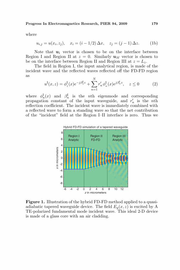
For simplicity we assume that a general 2D waveguide deviceis embedded in a parallel-plate structure. It is horizontally dividedinto three regions with the FD-FD region sandwiched between twoanalytical regions. For this hybrid FD-FD method to work, the multi-layer structure in the input and the output region must be alignedwith the z-axis. To understand how we combine the three regions intoone self-consistent FD-FD formulation let us refer to Figure 2 wherewe show the layout of FD-FD grids. The unknowns are the FD-FDvariables in Region II. The center of the coordinate (0, 0) is assumedto located at the lower left corner of the FD-FD region. The centralfield component is Ey(x, z) for TE polarization and Hy(x, z) for TM.In FD region the field uII(x, z) is uniformly sampled into a rectangulararray of discrete points {ui,j} , where ui,j = uII(xi, zj). We shall groupthem into M column vectors each with a length N so that
uj =
u1,j...
uN,j
, j = 1, . . . , M, (1a)
Progress In Electromagnetics Research, PIER 94, 2009 179
where
ui,j = u(xi, zj), xi = (i− 1/2)∆x, zj = (j − 1)∆z. (1b)
Note that u1 vector is chosen to be on the interface betweenRegion I and Region II at z = 0. Similarly uM vector is chosen tobe on the interface between Region II and Region III at z = Lz.
The field in Region I, the input analytical region, is made of theincident wave and the reflected waves reflected off the FD-FD regionas
uI(x, z) = φI1(x)e−jβI
1z +N∑
n=1
r′nφIn(x)ejβI
nz, z ≤ 0 (2)
where φIn(x) and βI
n is the nth eigenmode and correspondingpropagation constant of the input waveguide, and r′n is the nthreflection coefficient. The incident wave is immediately combined witha reflected wave to form a standing wave so that the net contributionof the “incident” field at the Region I–II interface is zero. Thus we
z in micrometers
x in
mic
rom
ete
rs
Hybrid FD-FD simulation of a tapered waveguide
Region I Region II Region III
Analytic FD-FD Analytic
-6 -4 -2 0 2 4 6 8 10 12
-8
-6
-4
-2
0
2
4
6
8
Figure 1. Illustration of the hybrid FD-FD method applied to a quasi-adiabatic tapered waveguide device. The field Ey(x, z) is excited by ATE-polarized fundamental mode incident wave. This ideal 2-D deviceis made of a glass core with an air cladding.
180 Chang, Cheng, and Lu
have
uI(x, z) = −2jφI1(x) sin(βI
1z) +N∑
n=1rnφI
n(x)ejβI
nz, z ≤ 0
r′n ={
rn − 1, n = 1rn, n 6= 1 .
(3)
Note that rn is the new nth reflection coefficient. The field inRegion III, the output analytical region, is made of the transmittedwaves scattered off the FD-FD region as
uIII(x, z) =N∑
n=1
tnφIIIn
(x)e−jβIIIn (z−Lz). z > Lz (4)
Here φIIIn (x) and βIII
n is the nth eigenmode and correspondingpropagation constant of the exit waveguide while tn is the nthtransmission coefficient. For a parallel-plate waveguide filled with ahomogeneous dielectric material, the eigenmodes {φn(x)} are simplesinusoidal functions. The normalized eigenfunction of a TE-polarized
Figure 2. The Layout of the grid points in the FD-FD region showsa total of N × M unknowns in the Lz by Lx domain. The first andthe last column of grid vectors are auxiliary variables located in theanalytical regions.

Progress In Electromagnetics Research, PIER 94, 2009 181
field bounded by a pair perfectly electric conducting walls (PECWs)is given by
φn(x) =√
2Lx
sinnπx
Lx, βn =
√k2 −
(nπ
Lx
)2
, n = 1, . . . , N (5)
The normalized eigenfunction of a TE-polarized field bounded by apair perfectly magnetic conducting walls (PMCWs) is given by
φn(x) =√
εn
Lxcos
nπx
Lx, εn =
{1, n = 02, n ≥ 1 ,
βn =
√k2 −
(nπ
Lx
)2, n = 0, . . . , N − 1
(6)
Eigenmodes of other more complex cases can be obtained bynumerically solving for the mode characteristic functions [3].
2.2. FD Approximation of Helmholtz Equation
The Ey(x, z) component of the TE case satisfies the following 2-DHelmholtz equation:
∂2Ey
∂x2+
∂2Ey
∂z2+ n2(x, z)k2
0Ey = 0. (7)
Using superscripts e, h for polarization and subscripts c, u, d, l, rto denote relative spatial relation, i.e., center, up, down, left andright, we then apply the second-order accurate FD approximation tothe 2-D Helmholtz equation for a field point uc. This leads to thefive-point TE FD-FD formulae connecting the four neighboring pointsuu, ud, ul, ur.
ceuuu + ce
dud + cel ul + ce
rur + cecuc = 0,
ceu = ce
d =1
∆x2, ce
l = cer =
1∆z2
,
cec = n2k2
0 − (ceu + ce
d + cel + ce
r) .
(8a)
If the field point uc is located near by a material interface (as depictedby Figure 3), we must choose n2 as some “average” of n2(x, z) aroundthe reference field point uc. It is chosen to be the integration overrectangular box centered at the particular field point given below:
n2 ∆=1
∆x∆z
z+∆z/2∫
z−∆z/2
x+∆x/2∫
x−∆x/2
n2(x, z) dx dz. (8b)

182 Chang, Cheng, and Lu
For the TM case, the Hy(x, z) component satisfies the following 2-DHelmholtz equation:
∂
∂x
[1
n2(x, z)∂
∂xHy
]+
∂
∂z
[1
n2(x, z)∂
∂zHy
]+ k2
0Hy(x, z) = 0. (9)
To derive TM FD coefficients near a material interface, we musttake extra cares to ensure the continuity of tangential magnetic fieldand continuity of tangential electric field Et(x, z) which is related toHy(x, z) by
Et(x, y) =1
n2(x, z)∂
∂nHy(x, y). (10)
Some papers choose a local coordinate system consistent with thematerial interface [34, 35]. Local FD variables and FD coefficients arederived and used. They are related back to the global variables byinterpolation. Such methods are suitable for material with large indexcontrasts. However, they produce complex anisotropic coefficients forboth TE and TM cases, which make the coding very difficult. Wepropose to use a similar averaging scheme like the TE case for theTM coefficients. Consider the first term in Equation (9), using centraldifference approximation we have
∂
∂x
[1
n2(x, z)∂
∂xHy
]≈ 1
∆x
[A
n2(x+∆x/2, z)− B
n2(x−∆x/2, z)
]
A=∂uc
∂x
∣∣∣∣x=x+∆x/2
≈ uu − uc
∆x, B=
∂uc
∂x
∣∣∣∣x=x−∆x/2
≈ uc − ud
∆x.
(11)
∆x
ul
∆z
uu
uc ur
ud
Figure 3. FD-FD TE grid points near a material interface.

Progress In Electromagnetics Research, PIER 94, 2009 183
Applying similar operation to the second term of Equation (9) we willobtain the following FD-FD coefficients for TM case:
1n2
u
uu
∆x2+
1n2
d
ud
∆x2+
1n2
l
ul
∆z2+
1n2
r
ur
∆z2
+(
k20 −
[1n2
u
+1n2
d
]1
∆x2−
[1n2
l
+1n2
r
]1
∆z2
)uc = 0,
chuuu + ch
dud + chl ul + ch
rur + chc uc = 0,
chu =
1n2
u
1∆x2
, chd =
1n2
d
1∆x2
, chl =
1n2
l
1∆z2
, chr =
1n2
r
1∆z2
,
chc = k2
0 −(chu + ch
d + chl + ch
r
).
(12a)
Instead of using just one average as in the TE case, TM cases havefour different averages for the up, down, left and right TM coefficients.The central coefficient ch
c contains the term chu + ch
d + chl + ch
r whichis the sum of four neighboring coefficients. In addition, instead of thesquared index as in the TE case, TM-integration is performed over theinverse of squared index given below:
1n2
∆=1
∆x∆z
z+∆z/2∫
z−∆z/2
x+∆x/2∫
x−∆x/2
1n2(x, z)
dx dz. (12b)
The integration domain is a rectangular box shifted half a grid up,down, left, right according to the subscript of the coefficient. Figure 4further illustrates the four centers of integration in dotted circles.
The material-averaging formula for our FD-FD coefficients shouldreduce the well known “stair case effect” of plain FD methods. Thedetail error analysis on Equations (8a), (8b), (12a) and (12b) will beinvestigated in the near future.
2.3. Derivation of LM-TBC
So far we have derived FD-FD equation for all interior points inRegion II. Points belong to u1 and uM vectors are shared betweenthe FD-FD region and the analytical regions. FD points on u1 arecoupled to analytical points on u0. Also uM vector is coupled to uM+1
vector. The fundamental idea of LM-TBC is that we can express, usingthe layer modes in each analytical region, u0 vector in term of u1 anduM+1 vectors in term of uM via a full matrix.

184 Chang, Cheng, and Lu
Refer to Figure 2 we know that FD field points at Region I–IIinterface z = 0 can be computed from Equation (3) with the reflectioncoefficients as
ui,1 = uI(xi, z = 0) =N∑
n=1
rnφIn(xi). (13a)
Similarly we have
ui,0 = uI(xi,−∆z) = 2jφI1(xi) sin(βI
1∆z)+N∑
n=1
rnφIn(xi)e−jβI
n∆z (13b)
Let us define the eigenfunction matrix ΦL and the propagation matrixPL for the input waveguide region as
ΦL∆=
[ϕI
1, ϕI2, . . . , ϕ
IM
], ϕI
i∆=
φIi(x1)
φIi(x2)...
φIi(xN )
, (14a)
PL(∆z) ∆=
e−jβI1∆z . . . 0
0. . . 0
0 . . . e−jβIN∆z
. (14b)
Figure 4. FD-FD TM grid points near a material interface. The fourcircled points are centers of integration for TM coefficients.

Progress In Electromagnetics Research, PIER 94, 2009 185
Then we have
u0 =
u1,0...
uN,0
= 2j sin(βI
1∆z)ϕI1 + ΦL ·P(∆z) · r, (15a)
where
r ∆=
r1
r2...
rN
= Φ−1
L · u1. (15b)
Finally we obtain the equation that relates u0 to u1 and the incidentwave.
u0 = 2j sin(βI1∆z)ϕI
1 + AL · u1, AL = ΦL ·PL(∆z) ·Φ−1L . (16)
Note that Φ−1L can be approximated by the its own transpose ΦT
L forreal dielectric waveguide whose eigenfunctions are orthogonal to eachother and can be normalized. To relate uM+1 to uM , we evaluateEquation (4) at uM and uM+1 points. We have
ui,M = uIII(xi, Lz) =N∑
n=1
tnφIIIn
(xi), (17a)
and
ui,M+1 = uIII(xi, Lz + ∆z) =N∑
n=1
tnφIIIn
(xi)e−jβIIIn ∆z. (17b)
t =
t1t2...
tN
= Φ−1
R · uM . (17c)
uM+1 =
u1,(M+1)...
uN,(M+1)
= AR · uM , AR = ΦR ·PR(∆z) ·Φ−1
R . (17d)
Note that the eigenfunction matrix ΦR and the propagation matrix PR
in the exit waveguide region are defined by Equations (14a) and (14b)in a similar way.

186 Chang, Cheng, and Lu
2.4. Inverting the FD-FD Linear Equation
We now have FD-FD equations for all field points in the transitionregion. These variables are organized into M column vectors whichsatisfy a block tri-diagonal matrix equation with a bandwidth of2N + 1. Since research on finding robust iterative methods for solvingdiscretized Helmholtz equation is still being actively pursued, we turnto direct methods for the numerical solution of the banded matrixequation such as Gaussian elimination or the LU factorization. Bothmethods require about N3 · M floating point operations. A modernday high-end PC with 4GB memory can hold up a quarter millionvariables, i.e., N,M ≈ 500, and intermediate storage in core memory.The total run time for the largest problem is well under ten minutes.
3. FD-FD RESULTS AND VERIFICATION
To illustrate and verify numerical results computed by our proposedhybrid FD-FD method, we consider the following two problems, 1.two-dimensional (2-D) free space Green’s function (FSGF), 2. 2-DGreen’s function of a dielectric slab waveguide (SWGF). The FD-FDresults are compared with exact analytical solution or by the rigoroussemi-analytical method.
3.1. Two-dimensional Free Space Green’s Function
The Helmholtz equation for the two-D free space Green’s function dueto a line source located in the origin is given by [3]
(∇2t + k2
0
)G (x, z) = −δ(x)δ(z). (18a)
The analytic closed-form solution is in term of the Hankel function ofthe second kind as
G(ρ) = − j
4H
(2)0 (k0ρ), ρ =
√x2 + z2 (18b)
In Figure 5 we compute and plot the 2-D field distribution thefree-space Green’s function computed by our hybrid FD-FD methodand by using Equation (18b), the exact analytic expression. Due tosymmetry in x and z we show only a rectangular slice using Nx = 400by, Nz = 80 grids with the line source located at the lower right corner.For the hybrid FD-FD we set the discretization density Nλ = 32 whichis number of points per wavelength so that ∆x = ∆z = λ/Nλ. We useLM-TBC for the left computational boundary and an even-symmetry

Progress In Electromagnetics Research, PIER 94, 2009 187
boundary condition for the right and bottom boundaries. Since all theNz field points located on the top computational boundary are morethan ten wavelengths away from the line source, we may approximatethe field at uNx, k by a local plane wave coming at an angle
θk = tan−1 k∆z
Nx∆x, k = 0, 1, . . . , Nz. (19a)
Since θk ¿ 1, we use the following one-term TBC for grid points justabove the top boundary:
uNx+1,k = uNx, k · exp (−jk0 cos θk∆x) . (19b)
We see from comparing FD-FD images with those computed by theexact solution that both the one-term TBC and LM-TBC work verywell.
To compute and quantify the FD-FD errors, we zero out the lowerright 4 by 4 corner points to remove the field singularity. We alsonormalize the two complex field arrays so that the root mean square(RMS) value of each simulation is set to be one. The RMS error which
Two-D Green's function, FD-FD vs analytic
0
2
4
6
8
10
12
14
16
0 2 4 6 8 10 12 14z in microns
x in
mic
ron
s
(a) (b) (c) (d)
Figure 5. Real and imaginary part of the 2-D free space Green’sfunction. The line source is located at the lower right corner. (a)FD-FD real, (b) FD-FD imaginary, (c) analytic real and (d) analyticimaginary.
188 Chang, Cheng, and Lu
is defined as
EFDRMS =
{1
(Nz + 1)(Nx + 1)
Nz∑
k=0
Nx∑
i=0
|ui, k − u(xi, zk)|2}1/2
, (20)
where {ui, k} is the normalized complex FD-FD field and u(xi, zk) is thenormalized complex 2-D free-space Green’s function. Using Nλ = 32,we compute EPMCW
RMS = 0.16 for LM-TBC with a top PMCW andEPECW
RMS = 0.14 for LM-TBC with a top PECW. We will show that theRMS error of the combined field EMW+EW
RMS is reduced to .053.
3.2. Reducing LM-TBC Corner Reflection
Even though we take very careful steps processing the four FD-FDcomputational edges, we are still seeing quite significant amount ofreflected energy scattering off the top-left corner due to the upperPMCW in the LM-TBC region. It is known that the planar reflectioncoefficient from the PEMW changes sign when the wall is replaced by aPECW. To further reduce LM-TBC corner reflection all our hybrid FD-FD calculations in Figure 5 and all the remaining figures are computedas the average of the two independent FD-FD simulations each withan opposite wall type. In other words,
ui,j =12
(uPECW
i,j + uPMCWi,j
), for all i, j. (21)
This would help to cancel some but not all reflected power. Thenew EMW+EW
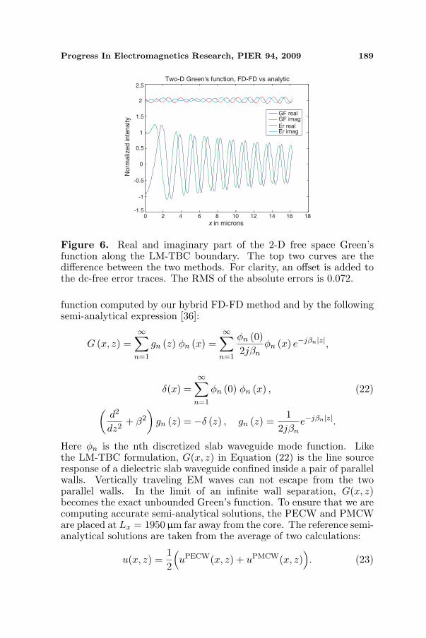
RMS is now reduced to .053 which is not much larger thanthe expected phase error produced by the standard five-point FDapproximation to the continuous Laplacian operator. The differencebetween the two calculations along the LM-TBC boundary is plottedon the top of Figure 6 along with the line plot of the exact 2-D Green’sfunction (GF). The RMS of absolute errors for this trace is 0.072. Forcomparison, the same RMS errors for the trace passes through the linesource is 0.029. We see that LM-TBC has done its job and producessmall difference from the exact solution. We also notice that the erroris greater near the corner where the two TBC boundaries meet.
3.3. Two-dimensional Green’s Function in an OpenDielectric Slab Waveguide
To verify LM-TBC’s performance in a layer structure, we plot inFigure 7, 2-D TE Ey(x, z) field distribution of slab waveguide Green’s
Progress In Electromagnetics Research, PIER 94, 2009 189
Two-D Green's function, FD-FD vs analytic
GF realGF imag
Er realEr imag
Norm
aliz
ed inte
nsity
2.5
2
1.5
1
0.5
0
-0.5
-1
-1.50 2 4 6 8 10 12 14 16 18
x in microns
Figure 6. Real and imaginary part of the 2-D free space Green’sfunction along the LM-TBC boundary. The top two curves are thedifference between the two methods. For clarity, an offset is added tothe dc-free error traces. The RMS of the absolute errors is 0.072.
function computed by our hybrid FD-FD method and by the followingsemi-analytical expression [36]:
G (x, z) =∞∑
n=1
gn (z) φn (x) =∞∑
n=1
φn (0)2jβn
φn (x) e−jβn|z|,
δ(x) =∞∑
n=1
φn (0) φn (x) , (22)
(d2
dz2+ β2
)gn (z) = −δ (z) , gn (z) =
12jβn
e−jβn|z|.
Here φn is the nth discretized slab waveguide mode function. Likethe LM-TBC formulation, G(x, z) in Equation (22) is the line sourceresponse of a dielectric slab waveguide confined inside a pair of parallelwalls. Vertically traveling EM waves can not escape from the twoparallel walls. In the limit of an infinite wall separation, G(x, z)becomes the exact unbounded Green’s function. To ensure that we arecomputing accurate semi-analytical solutions, the PECW and PMCWare placed at Lx = 1950µm far away from the core. The reference semi-analytical solutions are taken from the average of two calculations:
u(x, z) =12
(uPECW(x, z) + uPMCW(x, z)
). (23)
190 Chang, Cheng, and Lu
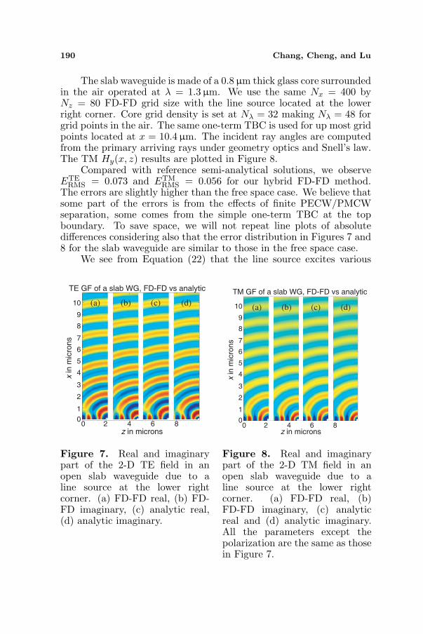
The slab waveguide is made of a 0.8 µm thick glass core surroundedin the air operated at λ = 1.3 µm. We use the same Nx = 400 byNz = 80 FD-FD grid size with the line source located at the lowerright corner. Core grid density is set at Nλ = 32 making Nλ = 48 forgrid points in the air. The same one-term TBC is used for up most gridpoints located at x = 10.4µm. The incident ray angles are computedfrom the primary arriving rays under geometry optics and Snell’s law.The TM Hy(x, z) results are plotted in Figure 8.
Compared with reference semi-analytical solutions, we observeETE
RMS = 0.073 and ETMRMS = 0.056 for our hybrid FD-FD method.
The errors are slightly higher than the free space case. We believe thatsome part of the errors is from the effects of finite PECW/PMCWseparation, some comes from the simple one-term TBC at the topboundary. To save space, we will not repeat line plots of absolutedifferences considering also that the error distribution in Figures 7 and8 for the slab waveguide are similar to those in the free space case.
We see from Equation (22) that the line source excites various
z in microns0 2 4 6 8
0
2
4
6
8
10
x in m
icro
ns
1
3
5
7
9
TE GF of a slab WG, FD-FD vs analytic
(a) (b) (c) (d)
Figure 7. Real and imaginarypart of the 2-D TE field in anopen slab waveguide due to aline source at the lower rightcorner. (a) FD-FD real, (b) FD-FD imaginary, (c) analytic real,(d) analytic imaginary.
(a) (b) (c) (d)
TM GF of a slab WG, FD-FD vs analytic
0
2
4
6
8
10
x in m
icro
ns
1
3
5
7
9
z in microns0 2 4 6 8
Figure 8. Real and imaginarypart of the 2-D TM field in anopen slab waveguide due to aline source at the lower rightcorner. (a) FD-FD real, (b)FD-FD imaginary, (c) analyticreal and (d) analytic imaginary.All the parameters except thepolarization are the same as thosein Figure 7.
Progress In Electromagnetics Research, PIER 94, 2009 191
modes in the slab waveguide. These mode fields are clearly transmittedoff the FD domain as there are visually no difference between the FDand the semi-analytical simulations. Thus, except near the FD corners,LM-TBC is capable of absorbing/transmitting all modes includingguiding modes, cladding modes and even evanescent waves across theFD-Analytic domain junction. We also notice from comparing Figure 7with Figure 8 that TM wave fields are better confined in the waveguidethan the TE wave fields.
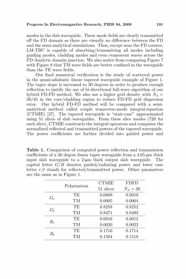
Our final numerical verification is the study of scattered powerin the quasi-adiabatic linear tapered waveguide example of Figure 1.The taper slope is increased to 30 degrees in order to produce enoughreflection to justify the use of bi-directional full-wave algorithm of ourhybrid FD-FD method. We also use a higher grid density with Nλ =30/45 in the core/cladding region to reduce FD-FD grid dispersionerror. Our hybrid FD-FD method will be compared with a semi-analytical method called couple transverse-mode integral-equation(CTMIE) [37]. The tapered waveguide is “stair-case” approximatedusing 51 slices of slab waveguides. From these slice modes (720 foreach slice), CTMIE constructs the integral operators and computes thenormalized reflected and transmitted powers of the tapered waveguide.The power coefficients are further divided into guided power and
Table 1. Comparison of computed power reflection and transmissioncoefficients of a 30 degree linear taper waveguide from a 4.65µm thickinput slab waveguide to a 2µm thick output slab waveguide. Thecapital letter G/R denotes guided/radiating power and lower caseletter r/t stands for reflected/transmitted power. Other parametersare the same as in Figure 1.
PolarizationCTMIE51 slices
FDFDNλ = 30
GrTETM
0.00090.0005
0.00100.0004
GtTETM
0.82580.8471
0.82520.8493
RrTETM
0.00160.0020
0.00120.0022
RtTETM
0.17160.1504
0.17140.1518

192 Chang, Cheng, and Lu
radiating power ratios. Both TE and TM polarization are comparedand the numerical results are listed in Table 1.
Although the relative errors in reflected power Gr and Rr are morethan 10 percents, the absolute values are very small. The much largertransmitted powers Gt and Gr agree with each other with a betterthan 99% accuracy. As a result, we are confident that both methodsproduce valid answers. Thus, the proposed hybrid FD-FD method issuitable for studying complex, small to medium size, optical waveguidedevices.
While LM-TBC is developed for the 2-D hybrid FDFD method,the boundary condition could be of interest to those FDTD researcherswho are interested in novel boundary conditions. It can be modifiedas a convolution operator to work with FDTD methods in 2D and 3Dapplications.
4. CONCLUSION
In this paper, we develop a hybrid FD-FD method suitable for studyingtwo-dimensional optical waveguide devices for both TE and TMpolarizations. Our layer-mode based transparent boundary condition,LM-TBC, is capable of launching an incident wave and simultaneously,directing the reflected and the transmitted scattered wave fields backand forward to the analytical regions. Using the exact free spaceGreen’s function, an “approximate” Green’s function for a dielectricslab waveguide and a semi-analytic solution to a linearly taperedwaveguide, we verify the effectiveness of our propose hybrid FD-FDmethod which allows us to solve for many complex 2-D waveguidedevices with horizontally stratified input/output waveguides.
ACKNOWLEDGMENT
We are grateful to the support of the National Science Council of theRepublic of China under the contracts NSC97-972221-E-110016. Thiswork is also supported by the Ministry of Education, Taiwan, underthe Aim-for-the-Top University Plan.
REFERENCES
1. Lin, C. F., Optical Components for Communications, KluwerAcademic Publishing, Boston, 2004.
2. Pavesi, L. and G. Guillot, Optical Interconnects, the SiliconApproach, Springer-Verlag, Berlin, 2006.
Progress In Electromagnetics Research, PIER 94, 2009 193
3. Ishimaru, A., Electromagnetic Propagation, Radiation, andScattering, Prentice Hall, Englewood Clifffs, N.J., 1991.
4. Chew, W.-C., Waves and Fields in Inhomogeneous Media, VanNorstrand Reinhold, New York, 1990.
5. Taflove, A. and S. Hagness, Computational Electrodynamics: TheFinite-difference Time-domain Method, Artech House, Norwood,MA, 2000.
6. Zheng, G., A. A. Kishk, A. W. Glisson, and A. B. Yakovlev,“A novel implementation of modified Maxwell’s equations inthe periodic finite-difference time-domain method,” Progress InElectromagnetics Research, PIER 59, 85–100, 2006.
7. Shao, W., S.-J. Lai, and T.-Z. Huang, “Compact 2-D full-waveorder-marching time-domain method with a memory-reducedtechnique,” Progress In Electromagnetics Research Letters, Vol. 6,157–164, 2009.
8. Yamauchi, J., Propagating Beam Analysis of Optical Waveguides,Research Studies Press, Baldock, England, 2003.
9. Yee, K. S., “Numerical solution of initial boundary value problemsinvolving Maxwell’s equations in isotropic media,” IEEE Trans.Antennas and Propagation, Vol. 14, 302–307, 1966.
10. Taflove, A. and M. Brodwin, “Numerical solution of steady-stateelectromagnetic scattering problem using the time-dependentMaxwell’s equations,” IEEE Trans. Microwave Theory andTechniques, Vol. 23, 623–630, 1975.
11. Taflove, A. and M. Brodwin, “Computation of the electromagneticfields and induced temperatures within a model of the microwave-irradiated human eye,” IEEE Trans. Microwave Theory andTechniques, Vol. 23, 888–896, 1975.
12. Holland, R., “Threde: A free-field EMP coupling and scatteringcode,” IEEE Trans. Nuclear Science, Vol. 24, 2416–2421, 1977.
13. Kunz, K. S. and K. M. Lee, “A three-dimensional finite-difference solution of the external response of an aircraft toa complex transient EM environment 1: The method and itsimplementation,” IEEE Trans. Electromagnetic Compatibility,Vol. 20, 328–333, 1978.
14. Huang, Y. C., “Study of absorbing boundary conditions for finitedifference time domain simulation of wave equations,” MasterThesis, Graduate Institute of Communication Engineering,National Taiwan University, June 2003.
15. Mur, G., “Absorbing boundary conditions for the finite differenceapproximation of the time domain electromagnetic field equation,”

194 Chang, Cheng, and Lu
IEEE Trans. Electromagnetic Compat. EMC-23, Vol. 4, 377–382,1981.
16. Lindman, E. L., “Free-space boundary conditions for the timedependent wave equation,” J. Comp. Phys., Vol. 18, 66–78, 1975.
17. Liao, Z. P., H. Wong, B. Yang, and Y. F. Yuan, “A transmittingboundary for transient wave analysis,” Scientia Sinica (Series A),Vol. 27, 1063–1076, 1984.
18. Grote, M. and J. Keller, “Nonreflecting boundary conditions fortime dependent scattering,” J. Comp. Phys., Vol. 127, 52–81,1996.
19. Engquist, B. and A. Majda, “Absorbing boundary conditions forthe numerical simulation of waves,” Math Comp., Vol. 31, 629–651, 1971.
20. Engquist, B. and A. Majda, “Radiation boundary conditions foracoustic and elastic wave calculations,” J. Comp. Phys., Vol. 127,52–81, 1996.
21. Hadley, G. R., “Transparent boundary conditions for the beampropagation method,” IEEE J. Quantum Electron, Vol. 28, 363–370, 1992.
22. Berenger, J. P., “A perfectly matched layer for the absorption ofelectromagnetic waves,” J. Comp. Phys., Vol. 114, 185–200, 1994.
23. Berenger, J. P., “Perfectly matched layer for the FDTD solutionof wave-structure interaction problems,” IEEE Trans. Antennasand Propagation, Vol. 44, No. 1. 110–117, 1996.
24. Zheng, K., W.-Y. Tam, D.-B. Ge, and J.-D. Xu, “Uniaxial PMLabsorbing boundary condition for truncating the boundary of dngmetamaterials,” Progress In Electromagnetics Research Letters,Vol. 8, 125–134, 2009.
25. Juntunen, J. S., “Zero reflection coefficient in discretized PML,”IEEE Microwave and Wireless Compt. Letter, Vol. 11, No. 4, 2001.
26. Johnson, S. G., “Notes on perfectly matched layers (PMLs), MIT18.369 and 18.336 course note, July 2008.
27. Hwang, J.-N., “A compact 2-D FDFD method for modelingmicrostrip structures with nonuniform grids and perfectlymatched layer,” Trans. on MTT., Vol. 53, 653-659, Feb. 2005.
28. Robertson, M. J., S. Ritchie, and P. Dayan, “Semiconductorwaveguides: Analysis of optical propagation in single ribstructures and directional couplers,” Inst. Elec. Eng. Proc.-J.,Vol. 132, 336–342, 1985.
29. Vassallo, C., “Improvement of finite difference methods for step-index optical waveguides,” Inst. Elec. Eng. Proc.-J., Vol. 139, 137–

Progress In Electromagnetics Research, PIER 94, 2009 195
142, 1992.30. Hua, Y., Q. Z. Liu, Y. L. Zou, and L. Sun, “A hybrid
FE-BI method for EM scattering from dielectric bodiespartiallycovered by conductors,” Journal of ElectromagneticWaves and Applications, Vol. 22, No. 2–3, 423–430, 2008.
31. Wang, S.-M., “Development of large-scale FDFD method forpassive optical devices,” Master Thesis (in Chinese), Instituteof Elctro-Optical Engineering, National Sun Yat-sen University,June 2005.
32. Chang, H. W. and W. C. Cheng, “Analysis of dielectric waveguidetermination with tilted facets by analytic continuity method,”Journal of Electromagnetic Waves and Applications, Vol. 21,No. 12, 1653–1662, 2007.
33. Cheng, W.-C. and H.-W. Chang, “Comparison of PML withlayer-mode based TBC for FD-FD method in a layered medium,”International Conference on Optics and Photonics in Taiwan, P1-170, Dec. 2008.
34. Chiang, Y. C., Y. Chiou, and H. C. Chang, “Improved full-vectorial finite-difference mode solver for optical waveguides withstep-index profiles,” J. of Lightwave Technology, Vol. 20, No. 8,1609–1618, August 2002.
35. Lavranos, C. S. and G. Kyriacou, “Eigenvalue analysis ofcurved waveguides employing an orthogonal curvilinear frequencydomain finite difference method,” IEEE Microwave Theory andTechniques, Vol. 57, 594–611, March 2009.
36. Magnanini, R. and F. Santosa, “Wave propagation in a 2-D opticalwaveguide,” SIAM J. Appl. Math., Vol. 61, No. 4. 1237–1252,2000.
37. Chang, H.-W. and M.-H. Sheng, “Field analysis of dielectricwaveguide devices based on coupled transverse-mode integralequation — Mathematical and numerical formulations,” ProgressIn Electromagnetics Research, PIER 78, 329–347, 2008.