
Laser Painting - pages.hmc.edu
27
1 Laser Painting E155 Final Project Report Dec. 10, 2006 Ronn Gruer and Cassie Chou Abstract Painting is an activity that many people enjoy. It has existed for centuries, and still remains at the forefront of artistic expression. However, it remains in its archaic form. Even with the advancements of our society, it is still required to have a brush and canvas in order for a person to paint. Furthermore, painting requires an artist to actually be right on top of his/her canvas. This project is a prototype for a solution to the artists’ struggle. The team has developed a laser painter to allow for easier painting. Sixty-four LED’s and corresponding phototransistors are soldered onto a “canvas,” so that the aspiring artist or ordinary E155 student can easily artistically express him/herself with LEDs!
Transcript of Laser Painting - pages.hmc.edu

1
Laser Painting E155 Final Project Report
Dec. 10, 2006 Ronn Gruer and Cassie Chou
Abstract Painting is an activity that many people enjoy. It has existed for centuries, and still remains at the forefront of artistic expression. However, it remains in its archaic form. Even with the advancements of our society, it is still required to have a brush and canvas in order for a person to paint. Furthermore, painting requires an artist to actually be right on top of his/her canvas. This project is a prototype for a solution to the artists’ struggle. The team has developed a laser painter to allow for easier painting. Sixty-four LED’s and corresponding phototransistors are soldered onto a “canvas,” so that the aspiring artist or ordinary E155 student can easily artistically express him/herself with LEDs!

2
Introduction The project can be split up into three systems: the FPGA, the PIC, and the hardware. The FPGA controls the phototransistors and the go_back button; the PIC controls the LEDs; and the hardware consists of the phototransistor and LED matrices. The entire project system structure is shown below, in Error! Reference source not found..
Figure 1: System Overview The FPGA is responsible for the phototransistor system. It is an extension of Lab 4 from E155. The FPGA takes inputs from the rows of the phototransistor matrix and outputs through the columns of the matrix. It polls through the columns of the phototransistor matrix and stops when an input on the phototransistor row has been detected. The FPGA also takes a go_back input from a push-button switch and outputs this to the PIC. Other outputs to the PIC include the encoded row and column phototransistor information and a change bit that signifies when new information has been received. The PIC is responsible for the LED system. It takes phototransistor inputs from the FPGA and stores or updates this information in memory. The PIC then outputs this information to the LED matrix. The PIC is also responsible for storing current data in the system in order to control the go back function. The PIC controls its memory update and go back functions through interrupt code and its multiplexed LED display through main code. The hardware component of the project ensures that the phototransistor voltage levels are not triggered by ambient light and will register as valid digital inputs. A reference phototransistor is placed at the bottom of the game board and serves as the reference voltage input to an op-amp comparator circuit. Each row of phototransistors goes through an op-amp comparator circuit in series with a diode to ensure that the phototransistor inputs to the FPGA are stable values. Another function of the hardware component is to ensure that the LEDs are functioning at high enough voltage levels. Because the system is multiplexing through eight columns, a 3.3V input is not enough to set off the LEDs. Therefore, an amplifying PNP transistor circuit is used for each row of LEDs.
3
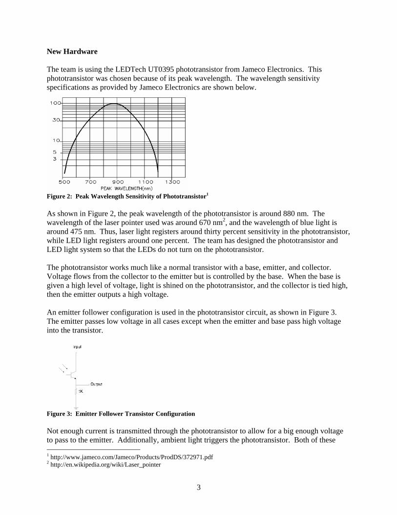
New Hardware The team is using the LEDTech UT0395 phototransistor from Jameco Electronics. This phototransistor was chosen because of its peak wavelength. The wavelength sensitivity specifications as provided by Jameco Electronics are shown below.
Figure 2: Peak Wavelength Sensitivity of Phototransistor1 As shown in Figure 2, the peak wavelength of the phototransistor is around 880 nm. The wavelength of the laser pointer used was around 670 nm2, and the wavelength of blue light is around 475 nm. Thus, laser light registers around thirty percent sensitivity in the phototransistor, while LED light registers around one percent. The team has designed the phototransistor and LED light system so that the LEDs do not turn on the phototransistor. The phototransistor works much like a normal transistor with a base, emitter, and collector. Voltage flows from the collector to the emitter but is controlled by the base. When the base is given a high level of voltage, light is shined on the phototransistor, and the collector is tied high, then the emitter outputs a high voltage. An emitter follower configuration is used in the phototransistor circuit, as shown in Figure 3. The emitter passes low voltage in all cases except when the emitter and base pass high voltage into the transistor.
Figure 3: Emitter Follower Transistor Configuration Not enough current is transmitted through the phototransistor to allow for a big enough voltage to pass to the emitter. Additionally, ambient light triggers the phototransistor. Both of these 1 http://www.jameco.com/Jameco/Products/ProdDS/372971.pdf 2 http://en.wikipedia.org/wiki/Laser_pointer

4
problems are solved by constructing a comparator circuit, which is show in Figure 4. A reference phototransistor is used to account for low current levels and ambient light. A difference in each comparator’s input voltage and ambient light voltage either drives the output to V+ or V-.
Figure 4: Comparator Circuit
Although the resistors used in each circuit are the same, the source voltages used are different. The reference phototransistor is powered with five volts, whereas all other phototransistors are powered with a TTL voltage of 3.3 volts. This will allow for different comparator input voltages when only ambient light is targeting the phototransistors.

5
Hardware Schematics
There are three systems, apart from the PIC and FPGA, in this project. These include the phototransistor system, the LED system, and the go back system. The phototransistors and LEDs are located close to each other on a separate board, so the user can easily see the target he/she is aiming for. The front cover of this report shows this phototransistor-LED spatial arrangement. The phototransistor system is made up of two basic subsystems: phototransistors and op-amps. The functionality of the phototransistors and op-amps is described in New Hardware. In summary, an emitter-follower transistor configuration is implemented to obtain proportionally different voltages on the emitter side when light is shined on the phototransistor; a reference photo sensor is used to cancel noise; and a comparator op-amp circuit is employed to amplify voltage as well as to convert analog outputs to digital outputs based on reference circuitry. The phototransistor display is presented in an eight-by-eight matrix, where each phototransistor is located next to its corresponding LED. A basic schematic of this design is shown in shown in Figure 9. On the actual board, there are eight row leads and eight column leads. In order to distinguish each phototransistor, the column, or collector side, is polled via the FPGA. Each row is basically tied to ground until one of the sixty-four sensors is triggered. When this occurs, the columns and rows “freeze” and processing through the Harris board occurs. Finally, a diode circuit is implemented after the comparator to reduce negative voltage to zero.
Figure 5: Phototransistor Circuitry

6
The LED circuitry is similar to that of the phototransistors and is shown below in Figure 6. There are sixty-four total diodes, arranged in an eight-by-eight matrix. Again, the rows and columns have eight leads each, which are both outputs of the PIC. The columns attach to the anode of each diode, while the rows attach to the cathodes. Therefore, in order for any LED to be on, the column must be high and the row set low. The team has implemented a multiplexing method in which only one column is on at a time. The columns are sorted through so quickly that the human eye sees that all columns are on at the same time. Furthermore, for this project to work, all rows need to be set high on a reset and at the start of the microcontroller program. The only other hardware for the LED system is PNP transistors. Before arriving at the LEDs, the column data is first passed through these transistors to amplify current. 3.3 volts was chosen as the emitter output voltage level instead of five volts, because row data is also output through the PIC at a TTL high voltage. If both were high, this would set off LEDs undesired.
Figure 6: LED Circuitry

7
The go back function has very simple hardware. It is only a switch that is tied high through a resistor. When pressed, the output is shorted to ground. A schematic can be seen below in Figure 7. The output for this circuitry is an input to the FPGA.
Figure 7: Go Back Function Circuitry

8
FPGA Design The FPGA handles the input systems of the project. These include the phototransistors and go back button. Sixteen phototransistor inputs and outputs, eight rows and eight columns, are used. Additionally, six additional outputs are used in order to send encoded row and column information to the PIC. The phototransistor system implements a scanning method to determine when a phototransistor is triggered. The rows, which are inputs into the FPGA, are originally set high through analog circuitry (see Appendix A), but change according to both user input and column values. Eight output column values poll with a single one and seven zeros. As long as the user does not trigger a phototransistor, the rows remain high. When a laser sets off a phototransistor, the column connects to a row and changes the subsequent row value. Two modules control phototransistor scanning. polling determines if the system is polling by ANDing the row values. scanning is a finite state machine that takes in the polling bit and outputs corresponding column values. If the polling bit is high, then the columns continually scan, whereas if polling is low then the column stays fixed in its current state. This is shown in Figure 8 below.
Figure 8: Polling Finite State Machine The next major component in the FPGA determines which row and column should be sent to the PIC. This is accomplished through a number of modules. The first module, start, establishes whether a phototransistor has been triggered. The FSM can be seen below, in Figure 9. While the phototransistors are polling, the module remains in State One. If phototransistors stop polling, the state machine moves to State Two, Three, and Four. In State Two and State Three, a bit called Enable is set high. The FSM stays in State Four until the system is polling again. The start module serves as debouncing circuitry and allows each trigger to only be registered for two clock cycles instead of for the entire time it is on.

9
Figure 9: Start Finite State Machine In parallel with this process, row and column data are encoded. These bits are outputted to the PIC. Row data also goes into a register to synchronize it with the enable bit from start, so that all information is synchronized on the same duty cycle. In the next step, the enable bit enables two registers: one that stores row data that has been triggered, and the stores the corresponding column data. This data is continually compared to the current row/column data, observing whether there is a difference between the two. If there is a difference in either the column or row comparisons and the enable bit is high, then an interrupt is sent to the PIC through a change bit, which is connected externally to RB5. If a phototransistor is triggered that is not the same as the last phototransistor triggered, then the PIC is interrupted. This takes care of the situation in which the user’s hand is shaking when he/she is pointing the laser at a phototransistor in the matrix. Finally, the FPGA controls the go back input. The go back input is sent through the start module so that the PIC does not receive a “go back” assertion more than once. The output of this module, which outputs from State Two and State Three, goes to the PIC.

10
Microcontroller Design The PIC system is responsible for LED outputs and memory storage. The PIC takes all of its inputs from the FPGA, and outputs directly to the LEDs on the game board. Inputs include encoded column data, encoded row data, a go back bit, and a change bit. Outputs include one-hot encoded LED row and column information. Memory storage is handled in the interrupt portion of the PIC code, and LED output is handled in the main portion of the code. The PIC system implements three memory blocks: two for the go back function that keep track of the most current row and column information (gbcol and gbrow), and one for the memory system that keeps track of the cumulative row information that should be displayed to the board of LEDs (col). These three arrays are declared initially in order to appropriately allocate memory. Additionally, the PIC code is set to interrupt on any changes in PORTB<7:4>. The team currently interrupts only on changes in bits five and four. LED Output System The main portion of the code is responsible displaying the output from the PIC through the LEDs. The LEDs are turned on by accessing system memory corresponding to the column and row of each phototransistor that has been triggered in the past. This value is held for 200 time cycles before moving on to the next column-row combination in order to avoid multiplexing issues with the LEDs. The code cycles through each column by accessing each column’s corresponding row information in this manner and thus multiplexes the LED output. Memory Update System The go back system consists of two arrays: one gb_col array and one gb_row array. Together, these two arrays keep track of the row and column information corresponding to the last phototransistor that was triggered. The go back column array stores row information corresponding to the column at which the last phototransistor was triggered. The go back pointer system is capable of both updating memory to incorporate the last LED that was turned on and turning off the last LED that was turned on. The go back bit is set through the FPGA when the user presses the go back button. This bit is sent to the PIC through RB4, and thus causes an interrupt to occur. When the code goes into the go back handling portion of the interrupt, a check is done to ensure that previous phototransistor input data actually exists in memory. The gbrow and gbcol pointers are then decremented in order to find the correct value corresponding with the last user input. The row information and stored pointer value corresponding to the appropriate column are XNORed to derive the sequence of information corresponding to the LEDs that should remain turned on. The change bit is set through the FPGA when the user triggers a phototransistor. This bit is sent to the PIC through RB5, and thus causes an interrupt to occur. When the code goes into the memory updating portion of the interrupt, encoded row and column information are decoded. The row information is then ANDed with the cumulative row information. The cumulative row information is found by accessing its corresponding location in the column array. gbrow and gbcol are then incremented. If the entire gb_col array stores more than four points, the code adjusts both memory blocks to save the last four data entries in each array.

11
Results The team has accomplished its goal of creating a laser pointer-guided painting game. The team has used a laser pointer, sixty-four LEDs, and sixty-four phototransistors to create this game. Additionally, eight op-amps and eight PNP bipolar-junction transistors were used in order to reach the team’s target current and voltage levels. A few changes were made from the original design as stated in the project proposal. The team implemented a go-back system that allows the user to go back four steps instead of one. The rationale behind this change in implementation is to allow the user more flexibility in using the game. Optimally, the project should be expanded to allow the user to go back ten or twenty steps, if desired. In this way, the user will not have to press the reset button every time he/she would like start from a blank board. Additionally, the team has implemented a limitation on the go-back system. The user cannot turn on an LED that has just been turned off through the go-back function. This has been implemented as an error-checking system, as there is no reason that a user would want to turn on a previously-“erased” LED. This change is implemented through the FPGA code, which disallows the same input from going through twice. The most difficult portion of this project lay in the soldering of the game board. Due to the way that the team had written its FPGA and microcontroller code, rows and columns of both phototransistors and LEDs needed to be soldered together. This added up to around six hundred solder joints. Additionally, the team had a moderately difficult time with the analog hardware component of the project. Because the team had ordered phototransistors and previous teams had used photodiodes, several components of the analog circuitry needed to be designed differently. These teams had also used 311 op-amps, whereas 411 op-amps were used in this project. Because of time constraints, the team was not able to optimize its microcontroller code. In its current state, the code contains several blocks that could be condensed into a for-loop that would be about five lines long. An example of this is shown in the code that multiplexes the LED output to Ports C and D.

12
Parts List Product Source Part Number Quantity Cost Total Cost Blue Ultra-Bright LED
All Electronics (www.allectronics.com) LED-122 64 0.65 41.6
Laser Pointer All Electronics (www.allectronics.com) LP-100 1 3.5 3.5
Phototransistor Jameco Electronics (www.jameco.com) UT0395-46-0125 64 0.28 17.92
Prototype Board R-Vac Electronics PHI 12-600 2 4.87 9.74411 Op Amp Electronics Lab 8 PNP BJT Electronics Lab 8
References
Harris, David. In-person interview. December 2006. Yang, Qimin. In-person interview. December 2006. Schaffer, Bob. In-person interview. December 2006. E155 2002 Laser Simon Project: <http://www3.hmc.edu/~harris/class/e155/projects02/simon.pdf> E155 2000 Laser Target Project: <http://www3.hmc.edu/~harris/class/e155/projects00/lasertargetgame.pdf> E155 2006 Lab 4 Results: < http://www3.hmc.edu/~harris/class/e155/lab4.pdf> Operational Amplifier Concepts: <http://hyperphysics.phy-astr.gsu.edu/hbase/electronic/opampcon.html#c1> Phototransistor Data Sheet: <http://www.jameco.com/Jameco/Products/ProdDS/372971.pdf>

13
Appendix A: Microcontroller Code /* laser_paint.c Written 11/18/06 by [email protected] [email protected] pulse width modulation (pwm) This code will display LED lights on a 8x8 matrix of LEDs given a phototransistor input from the FPGA. Additionally, a go_back function has been implemented that allows the user to "erase" the last LED that was triggered. Two systems of pointers were used to create the go_back system and are updated in the interrupt code. INPUTS PORTA<2:0> = FPGA Encoded Row Data PORTB<2:0> = FPGA Encoded Column Data PORTB<4> = FPGA Go Back Bit PORTB<5> = FPGA Enable Bit (signals incoming data) OUTPUTS PORTC<7:0> = PIC Row LED Output for a Specific Column PORTD<7:0> = PIC Column LED Output for a Specific Row */ #include <p18f452.h> #include <timers.h> /* Function Prototypes */ void main(void); void isr(void); //this is the interupt vector address //this tells the program to branch to the interupt code #pragma code low_vector = 0x08 void low_interrupt(void) { _asm GOTO isr _endasm } // Main code #pragma code int col[8] = {0xFF, 0xFF, 0xFF, 0xFF, 0xFF, 0xFF, 0xFF, 0xFF}; //Initialize row data int gb_col[6] = {0xFF, 0xFF, 0xFF, 0xFF, 0xFF, 0xFF}; //Initialize pointer system int gb_row[6] = {0xFF, 0xFF, 0xFF, 0xFF, 0xFF, 0xFF}; int *gbcol; //Initialize GoBack pointers int *gbrow; int *rowstart; //Create pointer for starting GoBack location void main(void) { // Multiplex through the columns int noop = 0; //Initialize delay values int upto = 200; gbcol = &gb_col[0]; //Initialize GoBack pointer locations gbrow = &gb_row[0]; PORTBbits.RB4 = 1; //Set the interrupt bit rowstart = gbrow; //Save initial row pointer value ADCON0 = 0x00; //Set A/D off ADCON1 = 0x07; TRISC = 0x00; //Output to LED row TRISD = 0x00; //Output to LED column TRISB = 0x7F; //Input from FPGA TRISE = 0x05; //Input from FPGA TRISA = 0xCF; //Input from FPGA INTCON = 0x00; //Set up so interrupt occurs only at RB<7:4> INTCONbits.GIE = 1; INTCONbits.RBIE = 1; INTCONbits.RBIF = 0; INTCON2bits.RBIP = 1; while(1) { // Multiplex through all columns with col[n]

14
// (row data) and delay for a while. PORTD = 0b01111111; //Column information PORTC = col[0]; //Row information while(noop < upto){ //Delay for a while noop++; } noop = 0; //Reset delay PORTC = 0xFF; //Clear PORTC so columns are independent PORTD = 0b10111111; PORTC = col[1]; while(noop < upto){ noop++; } noop = 0; PORTC = 0xFF; PORTD = 0b11011111; PORTC = col[2]; while(noop < upto){ noop++; } noop = 0; PORTC = 0xFF; PORTD = 0b11101111; PORTC = col[3]; while(noop < upto){ noop++; } noop = 0; PORTC = 0xFF; PORTD = 0b11110111; PORTC = col[4]; while(noop < upto){ noop++; } noop = 0; PORTC = 0xFF; PORTD = 0b11111011; PORTC = col[5]; while(noop < upto){ noop++; } noop = 0; PORTC = 0xFF; PORTD = 0b11111101; PORTC = col[6]; while(noop < upto){ noop++; } noop = 0; PORTC = 0xFF; PORTD = 0b11111110; PORTC = col[7]; while(noop < upto){ noop++; } noop = 0; PORTC = 0xFF; } } #pragma interruptlow isr //Interrupt triggers on PORTB<5:4> change void isr(void) { int temprow; int same;

15
int n; int portvar; int index; int noop = 0; if (PORTBbits.RB4 == 1) { // GoBack Handling
if (gbrow > rowstart){ // If pointer is not at first memory // location
gbrow = gbrow - 1; // Decrement both pointers gbcol = gbcol - 1; index = *gbcol; // Take the column index of GBCOL col[index] = ~(col[index] ^ *gbrow); // XNOR current row data with last
// triggered row LED (Gets the last // cumulative LED row data)
} } else if (PORTBbits.RB5 == 1) { // Phototransistor Trigger Handling temprow = 4*(PORTAbits.RA2) + 2*(PORTAbits.RA1) + (PORTAbits.RA0); // Assign row
// and column // variables // to store // new data
n = 4*(PORTBbits.RB2) + 2*(PORTBbits.RB1) + (PORTBbits.RB0); if (temprow == 0b000) { // Decode row data portvar = 0b01111111; } else if (temprow == 0b001) { portvar = 0b10111111; } else if (temprow == 0b010) { portvar = 0b11011111; } else if (temprow == 0b011) { portvar = 0b11101111; } else if (temprow == 0b100) { portvar = 0b11110111; } else if (temprow == 0b101) { portvar = 0b11111011; } else if (temprow == 0b110) { portvar = 0b11111101; } else if (temprow == 0b111){ portvar = 0b11111110; } else { portvar = 0b11111111; } same = col[n]; // Assign same to last stored row data col[n] = col[n] & portvar; // AND old row data with new row data
// (updates col[n]) same = same ^ col[n]; // XOR old row data with new row data if ((same != 0) && (same <= 0x00FF)){ // If old data != new row data,
// update pointers // Because the first eight bits can be // updated freely, we need the same <= // 0x00FF comparison to make sure they're // really different
*gbrow = portvar; // GoBack pointer gets current input gbrow = gbrow + 1; // Increment pointer *gbcol = n; // Do the same for GoBack column pointer gbcol = gbcol + 1; if (gbrow == rowstart + 5) { // If 5 spots have been filled, shift all
// data up by one & decrement pointers gbrow = gbrow - 1; gb_row[0] = gb_row[1]; gb_row[1] = gb_row[2]; gb_row[2] = gb_row[3]; gb_row[3] = gb_row[4]; gb_row[4] = gb_row[5];

16
gbcol = gbcol - 1; gb_col[0] = gb_col[1]; gb_col[1] = gb_col[2]; gb_col[2] = gb_col[3]; gb_col[3] = gb_col[4]; gb_col[4] = gb_col[5]; } } } PORTBbits.RB4 = 0; // Reset interrupt bits PORTBbits.RB5 = 0; INTCONbits.RBIF = 0; INTCONbits.RBIE = 1; }

17
Appendix B: FPGA Code `timescale 1ns / 1ps ////////////////////////////////////////////////////////////////////////////////// // Company: // Engineer: Ronn Gruer and Cassie Chou // Create Date: 20:01:43 11/12/2006 // Module Name: laser_painter ////////////////////////////////////////////////////////////////////////////////// // This Verilog module will take inputs from phototransistor rows and output to the // board as well as to the PIC. // ph_row: phototransistor row. If nothing is triggered then all rows are // set low.User-triggered. // clk: clock. FPGA-run through Harris utility board. // reset: reset. User-triggered through "FPGA RESET" button. // goback: go back is set high until the user pushes the go back button. // ph_col: phototransistor column. Output to phototransistors. // enc_col: encoded phototransistor column data. Output to PIC. // enc_row: encoded phototransistor row data. Output to PIC. // change: enable bit. Output to PIC (RB5). // cor_goback: go back output to PIC (RB4) ////////////////////////////////////////////////////////////////////////////////// module laser_painter(ph_row, clk, reset, goback, ph_col, enc_col, enc_row, change, cor_goback); input [7:0] ph_row; input clk; input reset; input goback; output [7:0] ph_col; output [2:0] enc_col; output [2:0] enc_row; output change; output cor_goback;
wire poll, nclk, invgb, comp_row, comp_col, enable, inter; wire [2:0] col, row; wire [7:0] invr, flop_row; counter cou9(clk, reset, nclk); //delays the clock polling ph_row_polling(ph_row, poll); // Determine if polling should stop. real_scanner scan(nclk, reset, poll, ph_col); // FSM Polling: next state // ~Polling: stay flop flop_row(nclk, ph_row, flop_row); // Register used to synchronize row
// with enable bit assign invr = ~flop_row; //invert row data to prepare for encoding ph_col_encoder encod(ph_col, enc_col); // Encode 8 bit column data to 3 bits ph_col_encoder rowencod(invr, enc_row); // Encode 8 bit row data to 3 bits start enabler(nclk, reset, poll, enable); // FSM Polling: go to 1st state
// ~Polling: go through 3 states // & stay in last until Polling is // asserted
assign invgb = ~goback; start enablergb(nclk, reset, invgb, cor_goback); // FSM to output go back bit enabled_reg3 regen3(nclk, enc_col, enable, col); // Enable flip flop: save last
// triggered column data enabled_reg3 regen3r(nclk, enc_row, enable, row); // Enable flip flop: save last
// triggered row data xnor_and rowxa(enc_row, row, comp_row); // Logic to determine if a new row
// was triggered xnor_and colxa(enc_col, col, comp_col); // Logic used to determine if a new
// column was triggered assign inter = comp_col | comp_row; // Logic used to determine if an
// interrupt should be sent to // PIC (RB5)
assign change = inter & enable; // These lines should be in their own // module, but Xilinx refused to
// build one. endmodule

18
`timescale 1ns / 1ps ////////////////////////////////////////////////////////////////////////////////// // Company: // Engineer: Ronn Gruer // // Create Date: 23:28:48 09/24/2006 // Design Name: // Module Name: counter // Description: This module is used to slow down the clock by 2^9. // clk: initial clock // reset: reset // d: output (delayed) clock ////////////////////////////////////////////////////////////////////////////////// module counter(clk, reset, d); input clk; input reset; output d; reg [9:0] q; // counter using always block always @(posedge clk, posedge reset) if (reset) q <= 10'b00_0000_0000; // If reset, start from 0 else q <= q+1; // Otherwise, increment q assign d = q[9]; // Assign output to last bit of q endmodule

19
`timescale 1ns / 1ps ////////////////////////////////////////////////////////////////////////////////// // Company: // Engineer: Ronn Gruer and Cassie Chou // // Create Date: 8:08:40 11/12/2006 // Design Name: // Module Name: polling // Description: This module determines whether the column data should be // polling or stay fixed // R: input row data // P: output polling bit ////////////////////////////////////////////////////////////////////////////////// module polling(R, P); input [7:0] R; output P; assign P= &R; // If all rows = 1, system is polling endmodule

20
`timescale 1ns / 1ps ////////////////////////////////////////////////////////////////////////////////// // Company: // Engineer: Ronn Gruer and Cassie Chou // // Create Date: 23:31:52 12/03/2006 // Module name: xnor_and // Description: This module is purely combinational logic that xor's two vectors // of data and then or's the output into one bit // a: one set of input data // b: one set of input data // y: output data ////////////////////////////////////////////////////////////////////////////////// module xnor_and(a, b, y); input [2:0] a; input [2:0] b; output y; wire [2:0] inter; assign inter = a ^ b; assign y = |inter; endmodule

21
`timescale 1ns / 1ps ////////////////////////////////////////////////////////////////////////////////// // Company: // Engineer: Ronn Gruer and Cassie Chou // // Create Date: 8:07:48 11/12/2006 // Design Name: // Module Name: scanner // Description: This module is a FSM that controls whether or not the // phototransistor columns are polling // clk: clock input // reset: triggered through reset button // poll: input bit that determines whether or not the system is polling // col: output phototransistor column ////////////////////////////////////////////////////////////////////////////////// module real_scanner(clk, reset, poll, col); input clk; input reset; input poll; output [7:0] col; reg [2:0] state, nextstate; parameter s0 = 3'b000; parameter s1 = 3'b001; parameter s2 = 3'b010; parameter s3 = 3'b011; parameter s4 = 3'b100; parameter s5 = 3'b101; parameter s6 = 3'b110; parameter s7 = 3'b111; //state register always @(posedge clk, posedge reset) if(reset) state <= s0; else state <= nextstate; //next state logic always @( * ) case(state) // If poll == 1 go to next state s0: if (poll) // Else stay in same state nextstate = s1; else nextstate = s0; s1: if (poll) nextstate = s2; else nextstate = s1; s2: if (poll) nextstate = s3; else nextstate = s2; s3: if (poll) nextstate = s4; else nextstate = s3; s4: if (poll) nextstate = s5; else nextstate = s4; s5: if (poll) nextstate = s6; else nextstate = s5; s6: if (poll) nextstate = s7; else nextstate = s6; s7: if (poll) nextstate = s0; else nextstate = s7; default: nextstate = s0;

22
endcase //output logic assign col[0] = (state==s0); // Each column is asserted in only a
// single state assign col[1] = (state==s1); assign col[2] = (state==s2); assign col[3] = (state==s3); assign col[4] = (state==s4); assign col[5] = (state==s5); assign col[6] = (state==s6); assign col[7] = (state==s7); endmodule
23
`timescale 1ns / 1ps ////////////////////////////////////////////////////////////////////////////////// // Company: // Engineer: Ronn Gruer and Cassie Chou // // Create Date: 22:31:21 11/19/2006 // Design Name: // Module Name: ebabled_reg3 // Description: This module is a simple enabled register. // clk: clock input // X: input data into register // Y: output data from register ////////////////////////////////////////////////////////////////////////////////// module enabled_reg3(clk, X, enable, Y); input clk; input [2:0] X; input enable; output reg [2:0] Y; always @(posedge clk) // Typical register with an enable bit if(enable) Y<=X; endmodule

24
`timescale 1ns / 1ps ////////////////////////////////////////////////////////////////////////////////// // Company: // Engineer: Ronn Gruer and Cassie Chou // // Create Date: 20:40:48 11/12/2006 // Design Name: // Module Name: START // Description: This module creates a debouncing state machine so that // its input will only be asserted for two clock cycles. // clk: clock input // reset: reset (triggered by reset button) // P: FSM input (polling) // enable: FSM output (enable bit) ////////////////////////////////////////////////////////////////////////////////// module start(clk, reset, P, enable); input clk; input reset; input P; output enable; reg [2:0] state, nextstate; parameter s0 = 3'b000; // Declare four states parameter s1 = 3'b001; parameter s2 = 3'b010; parameter s3 = 3'b011; //state register always @(posedge clk, posedge reset) if(reset) // Set the reset state to s0 state <= s0; else state <= nextstate; // Set all other states to next state //next state logic always @( * ) case(state) // If P is asserted, go to s0; s0: if (P) // Otherwise, s0 -> s1 -> s2 -> s3 ->
// stay in s3 nextstate = s0; else nextstate = s1; s1: if (P) nextstate = s0; else nextstate = s2; s2: if (P) nextstate = s0; else nextstate = s3; s3: if (P) nextstate = s0; else nextstate = s3; default: nextstate = s0; endcase //output logic assign enable = ((state == s1) | // Assign enable to only second two
(state == s2)); // states
endmodule

25
`timescale 1ns / 1ps ////////////////////////////////////////////////////////////////////////////////// // Company: // Engineer: Ronn Gruer and Cassie Chou // // Create Date: 20:21:46 11/12/2006 // Design Name: // Module Name: ph_col_decoder // Description: This module encodes one-hot data from eight bits to three bits // data: original data // decoded_data: encoded data ////////////////////////////////////////////////////////////////////////////////// module ph_col_encoder(data, decoded_data); input [7:0] data; output reg [2:0] decoded_data; always @ ( * ) case (data) 8'b1000_0000: decoded_data = 3'b000; 8'b0100_0000: decoded_data = 3'b001; 8'b0010_0000: decoded_data = 3'b010; 8'b0001_0000: decoded_data = 3'b011; 8'b0000_1000: decoded_data = 3'b100; 8'b0000_0100: decoded_data = 3'b101; 8'b0000_0010: decoded_data = 3'b110; 8'b0000_0001: decoded_data = 3'b111; default: decoded_data = 3'b000; // Default encoding: 000 endcase endmodule

26
`timescale 1ns / 1ps ////////////////////////////////////////////////////////////////////////////////// // Company: // Engineer: // // Create Date: 03:48:40 12/05/2006 // Design Name: // Module Name: flop // Description: Standard 7 bit flip flop (without enable) // clk: clock input // X: input into FF // Y: output from FF ////////////////////////////////////////////////////////////////////////////////// module flop(clk, X, Y); input clk; input [7:0] X; output reg [7:0] Y; always @(posedge clk) Y<=X; endmodule

27
Appendix C: FPGA Schematic
counter
cou9
polling
ph_row_polling
real_scanner
scan
flop
flop_row
ph_col_encoder
encod
ph_col_encoder
rowencod
start
enabler
start
enablergb
enabled_reg3
regen3
enabled_reg3
regen3r
xnor_and
rowxa
xnor_and
colxa
inter change
cor_goback
change
enc_row[2:0][2:0]
enc_col[2:0][2:0]
ph_col[7:0][7:0]
goback
resetclk
ph_row[7:0] [7:0]
clkreset d
[7:0] R[7:0] P
clkresetpoll
[7:0]col[7:0]
clk[7:0] X[7:0]
[7:0]Y[7:0]
[7:0] data[7:0] [2:0]decoded_data[2:0]
[7:0] data[7:0] [2:0]decoded_data[2:0]
clkresetP
enable
clkresetP
enable
clkenable
[2:0] X[2:0][2:0]Y[2:0]
clkenable
[2:0] X[2:0][2:0]Y[2:0]
[2:0] a[2:0][2:0] b[2:0] y
[2:0] a[2:0][2:0] b[2:0] y