Subsystems Datapath 11 - pages.hmc.edu
68
11 429 Datapath Subsystems 11.1 Introduction Chip functions generally can be divided into the following categories: Datapath operators Memory elements Control structures Special-purpose cells ○ I/O ○ Power distribution ○ Clock generation and distribution ○ Analog and RF CMOS system design consists of partitioning the system into subsystems of the types listed above. Many options exist that make trade-offs between speed, density, programma- bility, ease of design, and other variables. This chapter addresses design options for com- mon datapath operators. The next chapter addresses arrays, especially those used for memory. Control structures are most commonly coded in a hardware description language and synthesized. Special-purpose subsystems are considered in Chapter 13. As introduced in Chapter 1, datapath operators benefit from the structured design principles of hierarchy, regularity, modularity, and locality. They may use N identical cir- cuits to process N-bit data. Related data operators are placed physically adjacent to each other to reduce wire length and delay. Generally, data is arranged to flow in one direction, while control signals are introduced in a direction orthogonal to the dataflow. Common datapath operators considered in this chapter include adders, one/zero detectors, comparators, counters, Boolean logic units, error-correcting code blocks, shifters, and multipliers. 11.2 Addition/Subtraction “Multitudes of contrivances were designed, and almost endless drawings made, for the purpose of economizing the time and simplifying the mechanism of carriage.” —Charles Babbage, on Difference Engine No. 1, 1864 [Morrison61]
Transcript of Subsystems Datapath 11 - pages.hmc.edu

11
429
DatapathSubsystems
11.1
Introduction
Chip functions generally can be divided into the following categories:
�
Datapath operators
�
Memory elements
�
Control structures
�
Special-purpose cells
○
I/O
○
Power distribution
○
Clock generation and distribution
○
Analog and RF
CMOS system design consists of partitioning the system into subsystems of the typeslisted above. Many options exist that make trade-offs between speed, density, programma-bility, ease of design, and other variables. This chapter addresses design options for com-mon datapath operators. The next chapter addresses arrays, especially those used formemory. Control structures are most commonly coded in a hardware description languageand synthesized. Special-purpose subsystems are considered in Chapter 13.
As introduced in Chapter 1, datapath operators benefit from the structured designprinciples of hierarchy, regularity, modularity, and locality. They may use
N
identical cir-cuits to process
N
-bit data. Related data operators are placed physically adjacent to eachother to reduce wire length and delay. Generally, data is arranged to flow in one direction,while control signals are introduced in a direction orthogonal to the dataflow.
Common datapath operators considered in this chapter include adders, one/zerodetectors, comparators, counters, Boolean logic units, error-correcting code blocks,shifters, and multipliers.
11.2
Addition/Subtraction
“Multitudes of contrivances were designed, and almost endless drawings made, for the purpose of economizing the time and simplifying the mechanism of carriage.”
—Charles Babbage, on Difference Engine No. 1, 1864 [Morrison61]

Chapter 11 Datapath Subsystems
430
Addition forms the basis for many processing operations, from ALUs to address genera-tion to multiplication to filtering. As a result, adder circuits that add two binary numbersare of great interest to digital system designers. An extensive, almost endless, assortmentof adder architectures serve different speed/power/area requirements. This section beginswith half adders and full adders for single-bit addition. It then considers a plethora ofcarry-propagate adders (CPAs) for the addition of multibit words. Finally, related struc-tures such as subtracters and multiple-input adders are discussed.
11.2.1 Single-Bit Addition
The
half adder
of Figure 11.1(a) adds two single-bit inputs,
A
and
B
. The result is 0, 1, or2, so two bits are required to represent the value; they are called the sum
S
and carry-out
C
out
. The carry-out is equivalent to a carry-in to the next more significant column of amultibit adder, so it can be described as having double the
weight
of the other bits. If mul-tiple adders are to be cascaded, each must be able to receive the carry-in. Such a
full adder
as shown in Figure 11.1(b) has a third input called
C
or
C
in
. The truth tables for the half adder and full adder are given in Tables 11.1 and 11.2.
For a full adder, it is sometimes useful to define
Generate
(
G
),
Propagate
(
P
), and
Kill
(
K
)signals. The adder generates a carry when
C
out
is true independent of
C
in
, so
G
=
A · B
.The adder kills a carry when
C
out
is false independent of
C
in
, so
K
=
A · B
=
A
+
B
. Theadder propagates a carry; i.e., it produces a carry-out if and only if it receives a carry-in,when exactly one input is true:
P
=
A
⊕
B
.
From the truth table, the half adder logic is
(11.1)
TABLE 11.1
Truth table for half adder
A B C
out
S
0 0 0 00 1 0 11 0 0 11 1 1 0
TABLE 11.2
Truth table for full adder
A B C G P K C
out
S
0 0 0 0 0 1 0 01 0 1
0 1 0 0 1 0 0 11 1 0
1 0 0 0 1 0 0 11 1 0
1 1 0 1 0 0 1 01 1 1
S A BC A B
= ⊕=out ·
A B
C
S
Cout
A B
S
Cout
(a) (b)
FIGURE 11.1 Half and full adders

11.2 Addition/Subtraction
431
and the full adder logic is
(11.2)
The most straightforward approach to designing an adder is with logic gates. Figure11.2 shows a half adder. Figure 11.3 shows a full adder at the gate (a) and transistor (b)levels. The carry gate is also called a
majority
gate because it produces a 1 if at least two ofthe three inputs are 1. Full adders are used most often, so they will receive the attention ofthe remainder of this section.
S ABC ABC ABC ABC
A B C P C
C AB AC BC
AB C
= + + += ⊕( ) ⊕ = ⊕
= + +
= +out
AA B
AB C A B
A B C
+( )= + +( )= MAJ( , , )
AB
AB
S
Cout
FIGURE 11.2 Half adder design
ABC
S
Cout
(a)M
AJ
ABC
A
B BB
A
CS
C
CC
B BB
A A
(b)
A B
C
B
A
CBA A B C
Cout
C
A
A
BB
FIGURE 11.3 Full adder design
The full adder of Figure 11.3(b) employs 32 transistors (6 for the inverters, 10 for themajority gate, and 16 for the 3-input XOR). A more compact design is based on theobservation that
S
can be factored to reuse the
C
out
term as follows:
(11.3)
Such a design is shown at the gate (a) and transistor (b) levels in Figure 11.4 and usesonly 28 transistors. Note that the pMOS network is identical to the nMOS networkrather than being the conduction complement, so the topology is called a
mirror adder
.This simplification reduces the number of series transistors and makes the layout moreuniform. It is possible because the addition function is
symmetric
; i.e., the function of com-plemented inputs is the complement of the function.
The mirror adder has a greater delay to compute
S
than
C
out
. In carry-ripple adders(Section 11.2.2.1), the critical path goes from
C
to
C
out
through many full adders, so the
S ABC A B C C= + + +( ) out

Chapter 11 Datapath Subsystems
432
extra delay computing
S
is unimportant. Figure 11.4(c) shows the adder with transistorsizes optimized to favor the critical path using a number of techniques:
�
Feed the carry-in signal (
C
) to the inner inputs so the internal capacitance is already discharged.
�
Make all transistors in the sum logic whose gate signals are connected to the carry-in and carry logic minimum size (1 unit, e.g., 4
λ
). This minimizes the branching effort on the critical path. Keep routing on this signal as short as possible to reduce interconnect capacitance.
�
Determine widths of series transistors by logical effort and simulation. Build an asymmetric gate that reduces the logical effort from
C
to
C
out
at the expense of effort to
S
.
S
(a)
(b)
S
Cout
A B
C
B
A
Cout
C
A
A
BB
S
A B C
A B C
A
B
C
B
C
A
8 8
8
4
4 4 1
1
1
1
1
1
1
1
1 1
1 1 1
1
1
1
1
1
A
B
C
Cout
MINORITYABC Cout
Cout
SS
ABC
(c)
MINORITY
FIGURE 11.4 Full adder for carry-ripple operation
11.2 Addition/Subtraction
433
�
Use relatively large transistors on the critical path so that stray wiring capacitance is a small fraction of the overall capacitance.
�
Remove the output inverters and alternate positive and negative logic to reduce delay and transistor count to 24 (see Section 11.2.2.1).
Figure 11.5 shows two layouts of the adder (see also the inside front cover). Thechoice of the aspect ratio depends on the application. In a standard-cell environment, thelayout of Figure 11.5(a) might be appropriate when a single row of nMOS and pMOStransistors is used. The routing for the
A
,
B
, and
C
inputs is shown inside the cell,although it could be placed outside the cell because external routing tracks have to beassigned to these signals anyway. Figure 11.5(b) shows a layout that might be appropriatefor a dense datapath (if horizontal polysilicon is legal). Here, the transistors are rotatedand all of the wiring is completed in polysilicon and metal1. This allows metal2 bus linesto pass over the cell horizontally. Moreover, the widths of the transistors can increase
A
A
B C S Cout
VDD
GND
(a)
VDD
GNDA
B
C
(b)
S
Cout
FIGURE 11.5 Full adder layouts. Color version on inside front cover.

Chapter 11 Datapath Subsystems
434
without impacting the bit-pitch (height) of the datapath. In this case, the widths areselected to reduce the
C
in
to Cout delay that is on the critical path of a carry-ripple adder.A rather different full adder design uses transmission gates to form multiplexers and
XORs. Figure 11.6(a) shows the transistor-level schematic using 24 transistors and pro-viding buffered outputs of the proper polarity with equal delay. The design can be under-stood by parsing the transmission gate structures into multiplexers and an “invertibleinverter” XOR structure (see Section 11.7.4), as drawn in Figure 11.6(b).1 Note that themultiplexer choosing S is configured to compute P ⊕ C, as given in EQ (11.2).
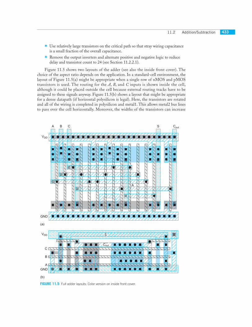
Figure 11.7 shows a complementary pass-transistor logic (CPL) approach. In com-parison to a poorly optimized 40-transistor static CMOS full adder, [Yano90] finds CPLis twice as fast, 30% lower in power, and slightly smaller. On the other hand, in compari-son to a careful implementation of the mirror adder, [Zimmermann97] finds the CPLdelay slightly better, the power comparable, and the area much larger.
Dynamic full adders are widely used in fast multipliers when power is not a concern.As the sum logic inherently requires true and complementary versions of the inputs, dual-rail domino is necessary. Figure 11.8 shows such an adder using footless dual-rail dominoXOR/XNOR and MAJORITY/MINORTY gates [Heikes94]. The delays to the twooutputs are reasonably well balanced, which is important for multipliers where both pathsare critical. It shares transistors in the sum gate to reduce transistor count and takes advan-tage of the symmetric property to provide identical layouts for the two carry gates.
Static CMOS full adders typically have a delay of 2–3 FO4 inverters, while dominoadders have a delay of about 1.5.
11.2.2 Carry-Propagate AdditionN-bit adders take inputs {AN, …, A1}, {BN, …, B1}, and carry-in Cin, and compute the sum{SN, …, S1} and the carry-out of the most significant bit Cout, as shown in Figure 11.9.
1Some switch-level simulators, notably IRSIM, are confused by this XOR structure and may not simulateit correctly.
B
S
Cout
BA C
P
P
A
1
0
1
0
P
P
C
S
Cout
(a) (b)
FIGURE 11.6 Transmission gate full adder
11.2 Addition/Subtraction 435
(Ordinarily, this text calls the least significant bit A0 rather than A1. However, for adders,the notation developed on subsequent pages is more graceful if column 0 is reserved tohandle the carry.) They are called carry-propagate adders (CPAs) because the carry intoeach bit can influence the carry into all subsequent bits. For example, Figure 11.10 showsthe addition 11112 + 00002 + 0/1, in which each of the sum and carry bits is influenced byCin. The simplest design is the carry-ripple adder in which the carry-out of one bit is sim-ply connected as the carry-in to the next. Faster adders look ahead to predict the carry-outof a multibit group. This is usually done by computing group PG signals to indicate
+
BN...1AN...1
SN...1
CinCout
FIGURE 11.9 Carry-propagate adder
A
C
S
S
B
B
C
C
C
B
B Cout
Cout
C
C
C
C
B
B
B
B
B
B
B
B
A
A
A
FIGURE 11.7 CPL full adder
Cout_h
A_h B_h
C_h
B_h
A_h
φCout_l
A_l B_l
C_l
B_l
A_l
φ
S_lS_h
A_h
B_h B_hB_l
A_l
C_lC_h C_h
φ
FIGURE 11.8 Dual-rail domino full

Chapter 11 Datapath Subsystems436
whether the multibit group will propagate a carry-in or will generate acarry-out. Long adders use multiple levels of lookahead structures foreven more speed.
11.2.2.1 Carry-Ripple Adder An N-bit adder can be constructed bycascading N full adders, as shown in Figure 11.11(a) for N = 4. This iscalled a carry-ripple adder (or ripple-carry adder). The carry-out of biti, Ci, is the carry-in to bit i + 1. This carry is said to have twice theweight of the sum Si. The delay of the adder is set by the time for thecarries to ripple through the N stages, so the tC→Cout delay should beminimized.
This delay can be reduced by omitting the inverters on the out-puts, as was done in Figure 11.4(c). Because addition is a self-dualfunction (i.e., the function of complementary inputs is the comple-ment of the function), an inverting full adder receiving complemen-tary inputs produces true outputs. Figure 11.11(b) shows a carry-ripple adder built from inverting full adders. Every other stage oper-ates on complementary data. The delay inverting the adder inputs orsum outputs is off the critical ripple-carry path.
11.2.2.2 Carry Generation and Propagation This section introducesnotation commonly used in describing faster adders. Recall that the P(propagate) and G (generate) signals were defined in Section 11.2.1.We can generalize these signals to describe whether a group spanningbits i…j, inclusive, generate a carry or propagate a carry. A group ofbits generates a carry if its carry-out is true independent of the carry-in; it propagates a carry if its carry-out is true when there is a carry-in.These signals can be defined recursively for i ≥ k > j as
(11.4)
with the base case
(11.5)
In other words, a group generates a carry if the upper (more significant) or the lower por-tion generates and the upper portion propagates that carry. The group propagates a carry ifboth the upper and lower portions propagate the carry.2
The carry-in must be treated specially. Let us define C0 = Cin and CN = Cout. Then wecan define generate and propagate signals for bit 0 as
(11.6)
2Alternatively, many adders use Ki = Ai + Bi in place of Pi because OR is faster than XOR. The group logicuses the same gates: Gi:j = Gi:k + Ki:k · Gk–1:j and Ki:j = Ki:k · Kk–1:j. However, Pi = Ai ⊕ Bi is still requiredin EQ (11.7) to compute the final sum. It is sometimes renamed Xi or Ti to avoid ambiguity.
G G P G
P P Pi j i k i k k j
i j i k k j
: : : :
: : :
·
·
= +
=−
−
1
1
G G A BP P A B
i i i i i
i i i i i
:
:
·≡ =≡ = ⊕
G C
P0 0
0 0 0:
:
==
in
11111 1111 +0000 0000
A4...1
carries
B4...1
S4...1
CinCout
00000 1111 +0000 1111
CinCout
FIGURE 11.10 Example of carry propagation
CinCout
B1A1B2A2B3A3B4A4
S1S2S3S4
(a)
Cout Cin
B1A1B2A2B3A3B4A4
S1S2S3S4
(b)
C1C2C3
C1C2C3
FIGURE 11.11 4-bit carry-ripple adder

11.2 Addition/Subtraction 437
Observe that the carry into bit i is the carry-out of bit i–1 and is Ci–1 = Gi–1:0. This isan important relationship; group generate signals and carries will be used synonymously inthe subsequent sections. We can thus compute the sum for bit i using EQ (11.2) as
(11.7)
Hence, addition can be reduced to a three-step process:
1. Computing bitwise generate and propagate signals using EQs (11.5) and (11.6)
2. Combining PG signals to determine group generates Gi–1:0 for all N ≥ i ≥ 1 using EQ (11.4)
3. Calculating the sums using EQ (11.7)
These steps are illustrated in Figure 11.12. The first and third steps are routine, so most ofthe attention in the remainder of this section is devoted to alternatives for the group PGlogic with different trade-offs between speed, area, and complexity. Some of the hardwarecan be shared in the bitwise PG logic, as shown in Figure 11.13.
S P Gi i i= ⊕ −1 0:
S1
B1A1
P1G1
G0:0
S2
B2
P2G2
G1:0
A2
S3
B3A3
P3G3
G2:0
S4
B4
P4G4
G3:0
A4 Cin
G0 P0
1: Bitwise PG Logic
2: Group PG Logic
3: Sum LogicC0C1C2C3
Cout
C4
FIGURE 11.12 Addition with generate and propagate logic
Many notations are used in the literature to describe the groupPG logic. In general, PG logic is an example of a prefix computa-tion [Leighton92]. It accepts inputs {PN:N, …, P0:0} and {GN:N, …,G0:0} and computes the prefixes {GN:0, …, G0:0} using the relation-ship given in EQ (11.4). This relationship is given many names inthe literature including the delta operator, fundamental carry operator,and prefix operator. Many other problems such as priority encodingcan be posed as prefix computations and all the techniques used tobuild fast group PG logic will apply, as we will explore in Section11.10.
AiBi
Gi
Pi
FIGURE 11.13 Shared bitwise PG logic

Chapter 11 Datapath Subsystems438
EQ (11.4) defines valency-2 (also called radix-2) group PG logic because it combinespairs of smaller groups. It is also possible to define higher-valency group logic to use fewerstages of more complex gates [Beaumont-Smith99], as shown in EQ (11.8) and later inFigure 11.16(c). For example, in valency-4 group logic, a group propagates the carry if allfour portions propagate. A group generates a carry if the upper portion generates, the sec-ond portion generates and the upper propagates, the third generates and the upper twopropagate, or the lower generates and the upper three propagate.
Logical Effort teaches us that the best stage effort is about 4. Therefore, it is not neces-sarily better to build fewer stages of higher-valency gates; simulations or calculations shouldbe done to compare the alternatives for a given process technology and circuit family.
11.2.2.3 PG Carry-Ripple Addition The critical path of the carry-ripple adder passes fromcarry-in to carry-out along the carry chain majority gates. As the P and G signals will havealready stabilized by the time the carry arrives, we can use them to simplify the majorityfunction into an AND-OR gate:3
(11.9)
Because Ci = Gi:0, carry-ripple addition can now be viewed as the extreme case ofgroup PG logic in which a 1-bit group is combined with an i-bit group to form an (i+1)-bit group
(11.10)
In this extreme, the group propagate signals are never used and need not be com-puted. Figure 11.14 shows a 4-bit carry-ripple adder. The critical carry path now proceedsthrough a chain of AND-OR gates rather than a chain of majority gates. Figure 11.15illustrates the group PG logic for a 16-bit carry-ripple adder, where the AND-OR gatesin the group PG network are represented with gray cells.
Diagrams like these will be used to compare a variety of adder architectures in subse-quent sections. The diagrams use black cells, gray cells, and white buffers defined inFigure 11.16(a) for valency-2 cells. Black cells contain the group generate and propagatelogic (an AND-OR gate and an AND gate) defined in EQ (11.4). Gray cells containingonly the group generate logic are used at the final cell position in each column becauseonly the group generate signal is required to compute the sums. Buffers can be used tominimize the load on critical paths. Each line represents a bundle of the group generateand propagate signals (propagate signals are omitted after gray cells). The bitwise PG and
3Whenever positive logic such as AND-OR is described, you can also use an AOI gate and alternate pos-itive and negative polarity stages as was done in Figure 11.11(b) to save area and delay.
G G P G P P G P Pi j i k i k k l i k k l l m i k: : : : : : : :· · · ·= + + +− − −1 1 1 kk l l m m j
i k i k k l k l l
P G
G P G P G− − −
− − −= + +1 1 1
1 1 1
: : :
: : : :
· ·
:: : :
: : : :· · ·m l m m j
i j i k k l l m m
P G
P P P P P
+( )( )=
− −
− − −
1 1
1 1 11: j
i k l m j
⎫
⎬⎪
⎭⎪
≥ > > >( ) (11.8)
C A B A B C
A B A B C
G PC
i i i i i i
i i i i i
i i i
= + +( )= + ⊕( )= +
−
−
−
1
1
1
G G P Gi i i i: :·0 1 0= + −

11.2 Addition/Subtraction 439
S1
B1A1
P1G1
G0:0
S2
B2
P2G2
G1:0
A2
S3
B3A3
P3G3
G2:0
S4
B4
P4G4
G3:0
A4 Cin
G0 P0
C0C1C2C3
Cout
C4
FIGURE 11.14 4-bit carry-ripple adder using PG logic
Delay
0123456789101112131415
15:0 14:0 13:0 12:0 11:0 10:0 9:0 8:0 7:0 6:0 5:0 4:0 3:0 2:0 1:0 0:0
Bit Position
FIGURE 11.15 Carry-ripple adder group PG network

Chapter 11 Datapath Subsystems440
sum XORs are abstracted away in the top and bottom boxes and it is assumed that anAND-OR gate operates in parallel with the sum XORs to compute the carry-out:
(11.11)
The cells are arranged along the vertical axis according to the time at which theyoperate [Guyot97]. From Figure 11.15 it can be seen that the carry-ripple adder criticalpath delay is
(11.12)
where tpg is the delay of the 1-bit propagate/generate gates, tAO is the delay of the AND-OR gate in the gray cell, and txor is the delay of the final sum XOR. Such a delay estimateis only qualitative because it does not account for fanout or sizing.
C G G P GN N N Nout = = + −: :0 1 0
t t N t tpg AOripple xor= + −( ) +1
i:j
i:j
i:k k−1:j
i:j
i:j
i:k k−1:l l−1:m m−1:j
i:k k−1:j
i:j
Gi:k
Pk−1:j
Gk−1:j
Gi:j
Pi:j
Pi:k
Gi:k
Gk−1:j
Gi:j Gi:j
Pi:j
Gi:j
Pi:j
(a)
Gi:k
Gk−1:l
Gl−1:m
Gm−1:j
Gi:j
Pi:j
Pi:k
Pi:k
Pk−1:l
Pl−1:m
Pm−1:j
Gi:k
Pk−1:j
Gk−1:j
Gi:j
Pi:j
Pi:k
Gi:k
Gk−1:j
Gi:j Gi:j
Pi:j
Gi:j
Pi:j
Pi:k
Gi:j
Pi:j
Gi:j Gi:j
Pi:j
G i:j
P i:j
Gi:k
Pi:k
Gk−1:j
Gi:k
Pi:k
Gk−1:j
Pk−1:j
(b)
Odd Rows
Even Rows
Black Cell Gray Cell Buffer
(c)
FIGURE 11.16 Group PG cells

11.2 Addition/Subtraction 441
Often, using noninverting gates leads to more stages of logic than are necessary. Fig-ure 11.16(b) shows how to alternate two types of inverting stages on alternate rows of thegroup PG network to remove extraneous inverters. For best performance, Gk–1:j shoulddrive the inner transistor in the series stack. You can also reduce the number of stages byusing higher-valency cells, as shown in Figure 11.16(c) for a valency-4 black cell.
11.2.2.4 Manchester Carry Chain Adder This section is available in the online Web Enhancedchapter at www.cmosvlsi.com.
11.2.2.5 Carry-Skip Adder The critical path of CPAs considered so far involves a gate ortransistor for each bit of the adder, which can be slow for large adders. The carry-skip (alsocalled carry-bypass) adder, first proposed by Charles Babbage in the nineteenth centuryand used for many years in mechanical calculators, shortens the critical path by computingthe group propagate signals for each carry chain and using this to skip over long carry rip-ples [Morgan59, Lehman61]. Figure 11.17 shows a carry skip adder built from 4-bitgroups. The rectangles compute the bitwise propagate and generate signals (as in Figure11.15), and also contain a 4-input AND gate for the propagate signal of the 4-bit group.The skip multiplexer selects the group carry-in if the group propagate is true or the rippleadder carry-out otherwise.
The critical path through Figure 11.17 begins with generating a carry from bit 1, andthen propagating it through the remainder of the adder. The carry must ripple through thenext three bits, but then may skip across the next two 4-bit blocks. Finally, it must ripplethrough the final 4-bit block to produce the sums. This is illustrated in Figure 11.18. The4-bit ripple chains at the top of the diagram determine if each group generates a carry. Thecarry skip chain in the middle of the diagram skips across 4-bit blocks. Finally, the 4-bitripple chains with the blue lines represent the same adders that can produce a carry-outwhen a carry-in is bypassed to them. Note that the final AND-OR and column 16 are notstrictly necessary because Cout can be computed in parallel with the sum XORs usingEQ (11.11).
The critical path of the adder from Figures 11.17 and 11.18 involves the initial PGlogic producing a carry out of bit 1, three AND-OR gates rippling it to bit 4, three multi-plexers bypassing it to C12, 3 AND-OR gates rippling through bit 15, and a final XOR toproduce S16. The multiplexer is an AND22-OR function, so it is slightly slower than theAND-OR function. In general, an N-bit carry-skip adder using k n-bit groups (N = n × k)has a delay of
(11.13)
WEBENHANCED
t t n t k t tpg AOskip mux xor= + −( ) + − +2 1 1( )
Cin+
S4:1
A4:1 B4:1
+
S8:5
A8:5 B8:5
+
S12:9
A12:9 B12:9
+
S16:13
A16:13 B16:13
Cout
C4 1
0
C8 1
0
C12 1
0
1
0
P8:5P12:9P16:13 P4:1
FIGURE 11.17 Carry-skip adder

Chapter 11 Datapath Subsystems442
This critical path depends on the length of the first and last group and the number ofgroups. In the more significant bits of the network, the ripple results are available early.Thus, the critical path could be shortened by using shorter groups at the beginning andend and longer groups in the middle. Figure 11.19 shows such a PG network using groupsof length [2, 3, 4, 4, 3], as opposed to [4, 4, 4, 4], which saves two levels of logic in a 16-bit adder.
The hardware cost of a carry-skip adder is equal to that of a simple carry-ripple adderplus k multiplexers and k n-input AND gates. It is attractive when ripple-carry adders aretoo slow, but the hardware cost must still be kept low. For long adders, you could use amultilevel skip approach to skip across the skips. A great deal of research has gone intochoosing the best group size and number of levels [Majerski67, Oklobdzija85, Guyot87,Chan90, Kantabutra91], although now, parallel prefix adders are generally used for longadders instead.
012345678910111213141516
15:0 14:0 13:0 12:0 11:0 10:0 9:0 8:0 7:0 6:0 5:0 4:0 3:0 2:0 1:0 0:016:0
FIGURE 11.18 Carry-skip adder PG network
012345678910111213141516
15:0 14:0 13:0 12:0 11:0 10:0 9:0 8:0 7:0 6:0 5:0 4:0 3:0 2:0 1:0 0:016:0
FIGURE 11.19 Variable group size carry-skip adder PG network

11.2 Addition/Subtraction 443
It might be tempting to replace each skip multiplexer in Figures 11.17 and 11.18 withan AND-OR gate combining the carry-out of the n-bit adder or the group carry-in andgroup propagate. Indeed, this works for domino-carry skip adders in which the carry outis precharged each cycle; it also works for carry-lookahead adders and carry-select adderscovered in the subsequent section. However, it introduces a sneaky long critical path intoan ordinary carry-skip adder. Imagine summing 111…111 + 000…000 + Cin. All of thegroup propagate signals are true. If Cin = 1, every 4-bit block will produce a carry-out.When Cin falls, the falling carry signal must ripple through all N bits because of the paththrough the carry out of each n-bit adder. Domino-carry skip adders avoid this pathbecause all of the carries are forced low during precharge, so they can use AND-OR gates.
Figure 11.20 shows how a Manchester carry chain from Section 11.2.2.4 can be mod-ified to perform carry skip [Chan90]. A valency-5 chain is used to skip across groups of 4bits at a time.
11.2.2.6 Carry-Lookahead Adder The carry-lookahead adder (CLA) [Weinberger58] issimilar to the carry-skip adder, but computes group generate signals as well as group prop-agate signals to avoid waiting for a ripple to determine if the first group generates a carry.Such an adder is shown in Figure 11.21 and its PG network is shown in Figure 11.22using valency-4 black cells to compute 4-bit group PG signals.
In general, a CLA using k groups of n bits each has a delay of
(11.14)t t t n k t tpg pg n AOcla xor= + + −( ) + −( )⎡⎣ ⎤⎦ +( ) 1 1
P2φ
G2
φ
G3
P3φ
G4
P4
G1
G2:0 G3:0
C4 (G4:0)
G1:0
φP1
φ
Cin (G0)
P4:1 Skip Path
φ
FIGURE 11.20 Carry-skip adder Manchester stage
Cin+
S4:1
G4:1P4:1
A4:1 B4:1
+
S8:5
G8:5P8:5
A8:5 B8:5
+
S12:9
G12:9P12:9
A12:9 B12:9
+
S16:13
G16:13P16:13
A16:13 B16:13
C4C8C12Cout
FIGURE 11.21 Carry-lookahead adder
Chapter 11 Datapath Subsystems444
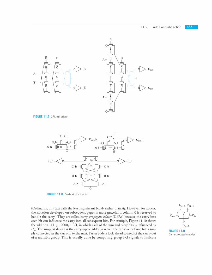
where tpg(n) is the delay of the AND-OR-AND-OR-…-AND-OR gate computing thevalency-n generate signal. This is no better than the variable-length carry-skip adder inFigure 11.19 and requires the extra n-bit generate gate, so the simple CLA is seldom agood design choice. However, it forms the basis for understanding faster adders presentedin the subsequent sections.
CLAs often use higher-valency cells to reduce the delay of the n-bit additions by com-puting the carries in parallel. Figure 11.23 shows such a CLA in which the 4-bit adders arebuilt using Manchester carry chains or multiple static gates operating in parallel.
11.2.2.7 Carry-Select, Carry-Increment, and Conditional-Sum Adders The critical pathof the carry-skip and carry-lookahead adders involves calculating the carry into each n-bitgroup, and then calculating the sums for each bit within the group based on the carry-in.A standard logic design technique to accelerate the critical path is to precompute the out-puts for both possible inputs, and then use a multiplexer to select between the two outputchoices. The carry-select adder [Bedrij62] shown in Figure 11.24 does this with a pair of
012345678910111213141516
15:0 14:0 13:0 12:0 11:0 10:0 9:0 8:0 7:0 6:0 5:0 4:0 3:0 2:0 1:0 0:016:0
FIGURE 11.22 Carry-lookahead adder group PG network
012345678910111213141516
15:0 14:0 13:0 12:0 11:0 10:0 9:0 8:0 7:0 6:0 5:0 4:0 3:0 2:0 1:0 0:016:0
FIGURE 11.23 Improved CLA group PG network

11.2 Addition/Subtraction 445
n-bit adders in each group. One adder calculates the sums assuming a carry-in of 0 whilethe other calculates the sums assuming a carry-in of 1. The actual carry triggers a multi-plexer that chooses the appropriate sum. The critical path delay is
(11.15)
The two n-bit adders are redundant in that both contain the initial PG logic and finalsum XOR. [Tyagi93] reduces the size by factoring out the common logic and simplifyingthe multiplexer to a gray cell, as shown in Figure 11.25. This is sometimes called a carry-increment adder [Zimmermann96]. It uses a short ripple chain of black cells to computethe PG signals for bits within a group. The bits spanned by each group are annotated onthe diagram. When the carry-out from the previous group becomes available, the finalgray cells in each column determine the carry-out, which is true if the group generates acarry or if the group propagates a carry and the previous group generated a carry. Thecarry-increment adder has about twice as many cells in the PG network as a carry-rippleadder. The critical path delay is about the same as that of a carry-select adder because amux and XOR are comparable, but the area is smaller.
(11.16)
t t n k t tpg AOselect mux= + + −⎡⎣ ⎤⎦ +( )2
t t n k t tpg AOincrement xor= + −( ) + −( )⎡⎣ ⎤⎦ +1 1
Cin+
A4:1 B4:1
S4:1
C4
+
+
1
A8:5 B8:5
S8:5
C8
+
+
A12:9 B12:9
S12:9
C12
+
+
A16:13 B16:13
S16:13
Cout
0
1
0
1
0
1
01 01 0
FIGURE 11.24 Carry-select adder
5:4
6:4
7:4
9:8
10:8
11:8
13:12
14:12
15:12
0123456789101112131415
15:0 14:0 13:0 12:0 11:0 10:0 9:0 8:0 7:0 6:0 5:0 4:0 3:0 2:0 1:0 0:0
FIGURE 11.25 Carry-increment adder PG network

Chapter 11 Datapath Subsystems446
Of course, Manchester carry chains or higher-valency cells can be used to speed theripple operation to produce the first group generate signal. In that case, the ripple delay isreplaced by a group PG gate delay and the critical path becomes
(11.17)
As with the carry-skip adder, the carry chains for the more significant bits completeearly. Again, we can use variable-length groups to take advantage of the extra time, asshown in Figure 11.26(a). With such a variable group size, the delay reduces to
(11.18)
The delay equations do not account for the fanout that each stage must drive. Thefanouts in a variable-length group can become large enough to require buffering betweenstages. Figure 11.26(b) shows how buffers can be inserted to reduce the branching effortwhile not impeding the critical lookahead path; this is a useful technique in many otherapplications.
In wide adders, we can recursively apply multiple levels of carry-select or carry-increment. For example, a 64-bit carry-select adder can be built from four 16-bit carry-
t t t k t tpg pg n AOincrement xor= + + −⎡⎣ ⎤⎦ +( ) 1
t t N t tpg AOincrement xor≈ + +2
3:25:4
6:4
8:7
9:7
12:11
13:11
14:11
15:11
10:7
(a)
(b)
3:25:4
6:4
8:7
9:7
12:11
13:11
14:11
15:11
10:7 6:0
3:0
1:0
0123456789101112131415
15:0 14:0 13:0 12:0 11:0 10:0 9:0 8:0 7:0 6:0 5:0 4:0 3:0 2:0 1:0 0:0
0123456789101112131415
15:0 14:0 13:0 12:0 11:0 10:0 9:0 8:0 7:0 6:0 5:0 4:0 3:0 2:0 1:0 0:0
FIGURE 11.26 Variable-length carry-increment adder

11.2 Addition/Subtraction 447
select adders, each of which selects the carry-in to the next 16-bit group. Taking this tothe limit, we obtain the conditional-sum adder [Sklansky60] that performs carry-selectstarting with groups of 1 bit and recursively doubling to N/2 bits. Figure 11.27 shows a16-bit conditional-sum adder. In the first two rows, full adders compute the sum andcarry-out for each bit assuming carries-in of 0 and 1, respectively. In the next two rows,multiplexer pairs select the sum and carry-out of the upper bit of each block of two, againassuming carries-in of 0 and 1. In the next two rows, multiplexers select the sum andcarry-out of the upper two bits of each block of four, and so forth.
Figure 11.28 shows the operation of a conditional-sum adder in action for N = 16with Cin = 0. In the block width 1 row, a pair of full adders compute the sum and carry-outfor each column. One adder operates assuming the carry-in to that column is 0, while theother assumes it is 1. In the block width 2 row, the adder selects the sum for the upper halfof each block (the even-numbered columns) based on the carry-out of the lower half. Italso computes the carry-out of the pair of bits. Again, this is done twice, for both possibil-ities of carry-in to the block. In the block width 4 row, the adder again selects the sum forthe upper half based on the carry-out of the lower half and finds the carry-out of the entireblock. This process is repeated in subsequent rows until the 16-bit sum and the final carry-out are selected.
The conditional-sum adder involves nearly 2N full adders and 2N log2 N multiplexers.As with carry-select, the conditional-sum adder can be improved by factoring out the sumXORs and using AND-OR gates in place of multiplexers. This leads us to the Sklanskytree adder discussed in the next section.
11.2.2.8 Tree Adders For wide adders (roughly, N > 16 bits), the delay of carry-lookahead(or carry-skip or carry-select) adders becomes dominated by the delay of passing the carrythrough the lookahead stages. This delay can be reduced by looking ahead across the look-ahead blocks [Weinberger58]. In general, you can construct a multilevel tree of look-ahead
s
s
s
0
1
0
1
0
1
cscs
sc
0
1
0
1
sc
sc
0
1
0
1
cs
cs
cscs
cs
scs s s
s
s
0
1
0
1
cs
cs
cs
cs
scs
cs s
cs s
A0B0A1B1A2B2A3B3A4B4A5B5A6B6A7B7A14B14A15B15
S0S1S2S3S4S5S6S7S14S15Cout
BlockWidth
BlockCarry In
01
1
02
1
04
1
08
1
016
Cin
FIGURE 11.27 Conditional-sum adder

Chapter 11 Datapath Subsystems448
structures to achieve delay that grows with log N. Such adders are variously referred to astree adders, logarithmic adders, multilevel-lookahead adders, parallel-prefix adders, or simplylookahead adders. The last name appears occasionally in the literature, but is not recom-mended because it does not distinguish whether multiple levels of lookahead are used.
There are many ways to build the lookahead tree that offer trade-offs among thenumber of stages of logic, the number of logic gates, the maximum fanout on each gate,and the amount of wiring between stages. Three fundamental trees are the Brent-Kung,Sklansky, and Kogge-Stone architectures. We begin by examining each in the valency-2case that combines pairs of groups at each stage.
The Brent-Kung tree [Brent82] (Figure 11.29(a)) computes prefixes for 2-bit groups.These are used to find prefixes for 4-bit groups, which in turn are used to find prefixes for8-bit groups, and so forth. The prefixes then fan back down to compute the carries-in toeach bit. The tree requires 2log2 N – 1 stages. The fanout is limited to 2 at each stage. Thediagram shows buffers used to minimize the fanout and loading on the gates, but in prac-tice, the buffers are generally omitted.
The Sklansky or divide-and-conquer tree [Sklansky60] (Figure 11.29(b)) reduces thedelay to log2 N stages by computing intermediate prefixes along with the large group pre-fixes. This comes at the expense of fanouts that double at each level: The gates fanout to[8, 4, 2, 1] other columns. These high fanouts cause poor performance on wide addersunless the high fanout gates are appropriately sized or the critical signals are bufferedbefore being used for the intermediate prefixes. Transistor sizing can cut into the regularityof the layout because multiple sizes of each cell are required, although the larger gates canspread into adjacent columns. Note that the recursive doubling in the Sklansky tree isanalogous to the conditional-sum adder of Figure 11.27. With appropriate buffering, thefanouts can be reduced to [8, 1, 1, 1], as explored in Exercise 11.7.
The Kogge-Stone tree [Kogge73] (Figure 11.29(c)) achieves both log2 N stages andfanout of 2 at each stage. This comes at the cost of many long wires that must be routedbetween stages. The tree also contains more PG cells; while this may not impact the area if
16 15 14 13 12 11 10 9 8 7 6 5 4 3 2 1BlockWidth
BlockCarry In
Block Sum and Carry Out
ab
sc
10
00
10
11
11
00
10
11
01
10
11
01
10
11
01
10
01
1scsc
02
1scsc
04
1scsc
08
1scsc
016
1sc
10
1001
11
01
11
01
11
01
11
01
11
01
1001
1001
1001
1001
1001
1001
1001
0010
0010
110
001
101
110
001
001
001
010
101
011
001
101
101
101
110
11001
10001
01001
00101
10101
00110
10110
110001001
001010110
101010110
01010110
11000100
Cin
0
Cout
Sum1
FIGURE 11.28 Conditional-sum addition example

11.2 Addition/Subtraction 449
the adder layout is on a regular grid, it will increase power consumption. Despite thesecosts, the Kogge-Stone tree is widely used in high-performance 32-bit and 64-bit adders.
In summary, a Sklansky or Kogge-Stone tree adder reduces the critical path to
(11.19)
An ideal tree adder would have log2 N levels of logic, fanout never exceeding 2, andno more than 1 wiring track (Gi:j and Pi:j bundle) between each row. The basic tree archi-tectures represent cases that approach the ideal, but each differ in one respect. Brent-Kung
t t N t tpg AOtree xor≈ + ⎡⎢ ⎤⎥ +log2
(a) Brent-Kung
(b) Sklansky
1:03:25:47:69:811:1013:1215:14
3:07:411:815:12
7:015:8
11:0
5:09:013:0
0123456789101112131415
15:0 14:0 13:0 12:0 11:0 10:0 9:0 8:0 7:0 6:0 5:0 4:0 3:0 2:0 1:0 0:0
1:0
2:03:0
3:25:47:69:811:1013:1215:14
6:47:410:811:814:1215:12
12:813:814:815:8
0123456789101112131415
15:0 14:0 13:0 12:0 11:0 10:0 9:0 8:0 7:0 6:0 5:0 4:0 3:0 2:0 1:0 0:0
15:0
(c) Kogge-Stone
1:02:13:24:35:46:57:68:79:810:911:1012:1113:1214:1315:14
3:04:15:26:37:48:59:610:711:812:913:1014:1115:12
4:05:06:07:08:19:210:311:412:513:614:715:8
2:0
0123456789101112131415
15:0 14:0 13:0 12:0 11:0 10:0 9:0 8:0 7:0 6:0 5:0 4:0 3:0 2:0 1:0 0:0
(e) Knowles [2,1,1,1]
1:02:13:24:35:46:57:68:79:810:911:1012:1113:1214:1315:14
3:04:15:26:37:48:59:610:711:812:913:1014:1115:12
4:05:06:07:08:19:210:311:412:513:614:715:8
2:0
0123456789101112131415
15:0 14:0 13:0 12:0 11:0 10:0 9:0 8:0 7:0 6:0 5:0 4:0 3:0 2:0 1:0 0:0
1:03:25:47:69:811:1013:12
3:07:411:815:12
5:07:013:815:8
15:14
15:8 13:0 11:0 9:0
0123456789101112131415
15:0 14:0 13:0 12:0 11:0 10:0 9:0 8:0 7:0 6:0 5:0 4:0 3:0 2:0 1:0 0:0
(f) Ladner-Fischer
1:03:25:47:69:811:1013:1215:14
3:05:27:49:611:813:1015:12
5:07:09:211:413:615:8
0123456789101112131415
15:0 14:0 13:0 12:0 11:0 10:0 9:0 8:0 7:0 6:0 5:0 4:0 3:0 2:0 1:0 0:0
(d) Han-Carlson
FIGURE 11.29 Tree adder PG networks

Chapter 11 Datapath Subsystems450
has too many logic levels. Sklansky has too much fanout. And Kogge-Stone has too manywires. Between these three extremes, the Han-Carlson, Ladner-Fischer, and Knowlestrees fill out the design space with different compromises between number of stages,fanout, and wire count.
The Han-Carlson trees [Han87] are a family of networks between Kogge-Stone andBrent-Kung. Figure 11.29(d) shows such a tree that performs Kogge-Stone on the odd-numbered bits, and then uses one more stage to ripple into the even positions.
The Knowles trees [Knowles01] are a family of networks between Kogge-Stone andSklansky. All of these trees have log2 N stages, but differ in the fanout and number ofwires. If we say that 16-bit Kogge-Stone and Sklansky adders drive fanouts of [1, 1, 1, 1]and [8, 4, 2, 1] other columns, respectively, the Knowles networks lie between theseextremes. For example, Figure 11.29(e) shows a [2, 1, 1, 1] Knowles tree that halves thenumber of wires in the final track at the expense of doubling the load on those wires.
The Ladner-Fischer trees [Ladner80] are a family of networks between Sklansky andBrent-Kung. Figure 11.29(f ) is similar to Sklansky, but computes prefixes for the odd-numbered bits and again uses one more stage to ripple into the even positions. Cells athigh-fanout nodes must still be sized or ganged appropriately to achieve good speed. Notethat some authors use Ladner-Fischer synonymously with Sklansky.
An advantage of the Brent-Kung network and those related to it (Han-Carlson andthe Ladner-Fischer network with the extra row) is that for any given row, there is nevermore than one cell in each pair of columns. These networks have low gate count. More-over, their layout may be only half as wide, reducing the length of the horizontal wiresspanning the adder. This reduces the wire capacitance, which may be a major componentof delay in 64-bit and larger adders [Huang00].
Figure 11.30 shows a 3-dimensional taxonomy of the tree adders [Harris03]. If we letL = log2 N, we can describe each tree with three integers (l, f, t) in the range [0, L – 1].The integers specify the following:
� Logic Levels: L + l� Fanout: 2 f + 1� Wiring Tracks: 2t
The tree adders lie on the plane l + f + t = L – 1. 16-bit Brent-Kung, Sklansky, andKogge-Stone represent vertices of the cube (3, 0, 0), (0, 3, 0) and (0, 0, 3), respectively.Han-Carlson, Ladner-Fischer, and Knowles lie along the diagonals.
11.2.2.9 Higher-Valency Tree Adders Any of the trees described so far can combinemore than two groups at each stage [Beaumont-Smith01]. The number of groups com-bined in each gate is called the valency or radix of the cell. For example, Figure 11.31shows 27-bit valency-3 Brent-Kung, Sklansky, Kogge-Stone, and Han-Carlson trees. Therounded boxes mark valency-3 carry chains (that could be constructed using a Manchestercarry chain, multiple-output domino gate, or several discrete gates). The trapezoids markcarry-increment operations. The higher-valency designs use fewer stages of logic, but eachstage has greater delay. This tends to be a poor trade-off in static CMOS circuits becausethe stage efforts become much larger than 4, but is good in domino because the logicalefforts are much smaller so fewer stages are necessary.
Nodes with large fanouts or long wires can use buffers. The prefix trees can also beinternally pipelined for extremely high-throughput operation. Some higher-valencydesigns combine the initial PG stage with the first level of PG merge. For example, the

11.2 Addition/Subtraction 451
Ling adder described in Section 11.2.2.11 computes generate and propagate for up to4-bit groups from the primary inputs in a single stage.
Higher valency (v) adders can still be described in a 3-dimensional taxonomy withL = logv N and l + f + t = L – 1. There are L + l logic levels, a maximum fanout of(v – 1)vf + 1, and (v – 1)vt wiring tracks at the worst level.
11.2.2.10 Sparse Tree Adders Building a prefix tree to compute carries in to every bit isexpensive in terms of power. An alternative is to only compute carries into short groups(e.g., s = 2, 4, 8, or 16 bits). Meanwhile, pairs of s-bit adders precompute the sums assum-ing both carries-in of 0 and 1 to each group. A multiplexer selects the correct sum for eachgroup based on the carries from the prefix tree. The group length can be balanced suchthat the carry-in and precomputed sums become available at about the same time. Such ahybrid between a prefix adder and a carry select adder is called a sparse tree. s is the sparse-ness of the tree.
The spanning-tree adder [Lynch92] is a sparse tree adder based on a higher-valencyBrent-Kung tree of Figure 11.31(a). Figure 11.32 shows a simple valency-3 version that
f (Fanout)
t (Wire Tracks)
l (Logic Levels)
0 (2)1 (3)
2 (5)
3 (9)
0 (4)
1 (5)
2 (6)
3 (8)
2 (4)
1 (2)
0 (1)
3 (7)
Kogge-Stone
Sklansky
Brent-Kung
Han-Carlson
Knowles[2,1,1,1]
Knowles[4,2,1,1]
Ladner-Fischer
Han-Carlson
Ladner-Fischer
New(1,1,1)
l + f + t = L − 1Plane
FIGURE 11.30 Taxonomy of prefix networks

Chapter 11 Datapath Subsystems452
01234567891011121314151617181920212223242526
15:0 14:0 13:0 12:0 11:0 10:0 9:0 8:0 7:0 6:0 5:0 4:0 3:0 2:0 1:0 0:026:0 25:0 24:0 23:0 22:0 21:0 20:0 19:0 18:0 17:0 16:0
01234567891011121314151617181920212223242526
15:0 14:0 13:0 12:0 11:0 10:0 9:0 8:0 7:0 6:0 5:0 4:0 3:0 2:0 1:0 0:026:0 25:0 24:0 23:0 22:0 21:0 20:0 19:0 18:0 17:0 16:0
01234567891011121314151617181920212223242526
15:0 14:0 13:0 12:0 11:0 10:0 9:0 8:0 7:0 6:0 5:0 4:0 3:0 2:0 1:0 0:026:0 25:0 24:0 23:0 22:0 21:0 20:0 19:0 18:0 17:0 16:0
(b) Sklansky
(c) Kogge-Stone
(a) Brent-Kung
01234567891011121314151617181920212223242526
15:0 14:0 13:0 12:0 11:0 10:0 9:0 8:0 7:0 6:0 5:0 4:0 3:0 2:0 1:0 0:026:0 25:0 24:0 23:0 22:0 21:0 20:0 19:0 18:0 17:0 16:0
(d) Han-Carlson
FIGURE 11.31 Higher-valency tree adders
0123456789101112131415161718192021222324252627
123456789101112131415161718192021222324252627Cout
FIGURE 11.32 Valency-3 Brent-Kung sparse tree adder with s = 3

11.2 Addition/Subtraction 453
precomputes sums for s = 3-bit groups and saves one logic level by selecting the outputbased on the carries into each group. The carry-out (Cout) is explicitly shown. Note thatthe least significant group requires a valency-4 gray cell to compute G3:0, the carry-in tothe second select block.
[Lynch92] describes a 56-bit spanning-tree design from the AMD AM29050floating-point unit using valency-4 stages and 8-bit carry select groups. [Kantabutra93]and [Blackburn96] describe optimizing the spanning-tree adder by using variable-lengthcarry-select stages and appropriately selecting transistor sizes.
A carry-select box spanning bits i…j is shown in Figure 11.33(a). It uses short carry-ripple adders to precompute the sums assuming carry-in of 0 and 1 to the group, and thenselects between them with a multiplexer, as shown in Figure 11.33(b). The adders can besimplified somewhat because the carry-ins are constant, as shown in Figure 11.33(c) for a4-bit group.
[Mathew03] describes a 32-bit sparse-tree adder using a valency-2 tree similar toSklansky to compute only the carries into each 4-bit group, as shown in Figure 11.34. Thisreduces the gate count and power consumption in the tree. The tree can also be viewed asa (2, 2, 0) Ladner-Fischer tree with the final two tree levels and XOR replaced by theselect multiplexer. The adder assumes the carry-in is 0 and does not produce a carry-out,saving one input to the least-significant gray box and eliminating the prefix logic in thefour most significant columns.
These sparse tree approaches are widely used in high-performance 32–64-bit higher-valency adders because they offer the small number of logic levels of higher-valency treeswhile reducing the gate count and power consumption in the tree. Figure 11.35 shows a27-bit valency-3 Kogge-Stone design with carry-select on 3-bit groups. Observe how thenumber of gates in the tree is reduced threefold. Moreover, because the number of wires isalso reduced, the extra area can be used for shielding to reduce path delay. This design canalso be viewed as the Han-Carlson adder of Figure 11.31(d) with the last logic levelreplaced by a carry-select multiplexer.
i j...
(a)
+
+
Ai:j Bi:j
Si:j
0
1
Gj − 1:0
(b)
P1
Cin
S1S2S3S4
P4P4 P2P2P3P3 P1
G1P1G1PG2PG3
(c)
Cin =Gj − 1:0
1 0 1 0 1 0 1 01 0
FIGURE 11.33 Carry-select implementation

Chapter 11 Datapath Subsystems454
Sparse trees reduce the costly part of the prefix tree. For Kogge-Stone architectures,they reduce the number of wires required by a factor of s. For Sklansky architectures, theyreduce the fanout by s. For Brent-Kung architectures, they eliminate the last logv s logiclevels. In effect, they can move an adder toward the origin in the (l, f, t) design space.These benefits come at the cost of a fanout of s to the final select multiplexer, and of areaand power to precompute the sums.
11.2.2.11 Ling Adders Ling discovered a technique to remove one series transistor fromthe critical group generate path through an adder at the expense of another XOR gate in thesum precomputation [Ling81, Doran88, Bewick94]. The technique depends on using K inplace of P in the prefix network, and on the observation that GiKi = (AiBi)(Ai + Bi) = Gi .
Define a pseudogenerate (sometimes called pseudo-carry) signal Hi : j = Gi + Gi-1: j. Thisis simpler than Gi : j = Gi + PiGi-1: j . Gi : j can be obtained later from Hi : j with an ANDoperation when it is needed:
(11.20)
The advantage of pseudogenerate signals over regular generate is that the first row in theprefix network is easier to compute.
Also define a pseudopropagate signal I that is simply a shifted version of propagate:Ii:j = Ki-1: j-1. Group pseudogenerate and pseudopropagate signals are combined using thesame black or gray cells as ordinary group generate and propagate signals, as you may showin Exercise 11.11.
(11.21)
K H K G K G G K G Gi i j i i i i j i i i j i j: : : := + = + =− −1 1
H H I H
I I Ii j i k i k k j
i j i k k j
: : : :
: : :
= +
=−
−
1
1
2:1
4:1
4:36:58:710:912:1114:1316:15
8:512:916:13
16:9 8:1
12:116:1
16 123456789101112131415
18:17
20:17
20:1922:2124:2326:2528:27
24:2128:25
24:17
28:17
32 171819202122232425262728293031
1234567891011121314151617181920212223242526272829303132
20:124:128:1 '0'
FIGURE 11.34 Intel valency-2 Sklansky sparse tree adder with s = 4
0123456789101112131415161718192021222324252627
123456789101112131415161718192021222324252627Cout
FIGURE 11.35 Valency-3 Kogge-Stone sparse tree adder with s = 3

11.2 Addition/Subtraction 455
The true group generate signals are formed from the pseudogenerates using EQ(11.20). These signals can be used to compute the sums with the usual XOR: Si =Pi ⊕ Gi–1:0 = Pi ⊕ (Ki–1Hi–1:0). To avoid introducing an AND gate back onto the criticalpath, we expand Si in terms of Hi–1:0
(11.22)
Thus, sum selection can be performed with a multiplexer choosing either Pi ⊕ Ki–1 or Pibased on Hi–1:0.
The Ling adder technique can be used with any form of adder that uses black andgray cells in a prefix network. It works with any valency and for both domino and staticdesigns. The initial PG stage and the first levels of the prefix network are replaced by a cellthat computes the group H and I signals directly. The middle of the prefix network isidentical to an ordinary prefix adder but operates on H and I instead of G and P. The sum-selection logic uses the multiplexer from EQ (11.22) rather than an XOR. In sparse trees,the sum out of s-bit blocks is selected directly based on the H signals.
For a valency-v adder, the Ling technique converts a generate gate with v seriesnMOS transistors and v series pMOS transistors to a pseudogenerate gate with v – 1 seriesnMOS but still v series pMOS. For example, in valency 2, the AOI gate becomes a NOR2gate. This is not particularly helpful for static logic, but is ben-eficial for domino implementations because the series pMOSare eliminated and the nMOS stacks are shortened.
Another advantage of the Ling technique is that it allowsthe first level pseudogenerate and pseudopropagate signals tobe computed directly from the Ai and Bi inputs rather thanbased on Gi and Ki gates. For example, Figure 11.36 comparesstatic gates that compute G2:1 and H2:1 directly from A2:1 andB2:1. The H gate has one fewer series transistor and much lessparasitic capacitance. H3:1 can also be computed directly fromA3:1 and B3:1 using the complex static CMOS gate shown inFigure 11.37(a) [Quach92]. Similarly, Figure 11.37(b) showsa compound domino gate that directly computes H4:1 from Aand B using only four series transistors rather than thefive required for G4:1 [Naffziger96, Naffziger98].
S H P K H Pi i i i i i= ⊕⎡⎣ ⎤⎦ + ⎡⎣ ⎤⎦− − −1 0 1 1 0: :
A1
B1
A2 B2A2
B2
A2 B2
A1 B1
A2
B2
G2:1
G2:1 = G2 + K2G1 = A2B2 + (A2 + B2)A1B1
H2:1 = G2 + G1 = A2B2 + A1B1
A1A2
B1B2
A2 B2
A1 B1
H2:1
(a) (b)
FIGURE 11.36 2-bit generate and pseudogenerate gates using primary inputs
A1
B1
A2 B2A2
B2
A2 B2
A1 B1
A2
B2
H3:1
(a) (b)
A3
φ
φ
B3
A2
B2
A2 B2
A1
B1
A3 B3H4:1
φ
A4
B4
H4:1 = G4 + G3 + K3(G2 + K2G1) = A4B4 + A3B3 + (A3 + B3)(A2B2 + (A2 + B2)A1B1)
H3:1 = G3 + G2 + K2G1 = A3B3 + A2B2 + (A2 + B2)A1B1
A3
B3
A3A3
FIGURE 11.37 3-bit and 4-bit pseudogenerate gates using primary inputs

Chapter 11 Datapath Subsystems456
[ Jackson04] proposed applying the Ling method recursively to factor out the K signalelsewhere in the adder tree. [Burgess09] showed that this recursive Ling technique opensup a new design space containing faster and smaller adders.
11.2.2.12 An Aside on Domino Implementation Issues This section is available in theonline Web Enhanced chapter at www.cmosvlsi.com.
11.2.2.13 Summary Having examined so many adders, you probably want to knowwhich adder should be used in which application. Table 11.3 compares the various adderarchitectures that have been illustrated with valency-2 prefix networks. The category“logic levels” gives the number of AND-OR gates in the critical path, excluding the initialPG logic and final XOR. Of course, the delay depends on the fanout and wire loads aswell as the number of logic levels. The category “cells” refers to the approximate number ofgray and black cells in the network. Carry-lookahead is not shown because it uses higher-valency cells. Carry-select is also not shown because it is larger than carry-increment forthe same performance.
In general, carry-ripple adders should be used when they meet timing constraintsbecause they use the least energy and are easy to build. When faster adders are required,carry-increment and carry-skip architectures work well for 8–16 bit lengths. Hybridscombining these techniques are also popular. At word lengths of 32 and especially 64 bits,tree adders are distinctly faster.
There is still debate about the best tree adder designs; the choice is influenced bypower and delay constraints, by domino vs. static and custom vs. synthesis choices, and bythe specific manufacturing process. Moreover, careful optimization of a particular archi-tecture is more important than the choice of tree architecture.
When power is no concern, the fastest adders use domino or compound domino cir-cuits [Naffziger96, Park00, Mathew03, Mathew05, Oklobdzija05, Zlatanovici09,Wijeratne07]. Several authors find that the Kogge-Stone architecture gives the lowest
TABLE 11.3 Comparison of adder architectures
Architecture Classification Logic Levels Max Fanout Tracks Cells
Carry-Ripple N – 1 1 1 NCarry-Skip
(n = 4)N/4 + 5 2 1 1.25N
Carry-Increment (n = 4)
N/4 + 2 4 1 2N
Carry-Increment (variable group)
1 2N
Brent-Kung (L–1, 0, 0) 2log2 N – 1 2 1 2NSklansky (0, L–1, 0) log2 N N/2 + 1 1 0.5 N log2 N
Kogge-Stone (0, 0, L – 1) log2 N 2 N/2 N log2 NHan-Carlson (1, 0, L – 2) log2 N + 1 2 N/4 0.5 N log2 N
Ladner Fischer (l = 1)
(1, L – 2, 0) log2 N + 1 N/4 + 1 1 0.25 N log2 N
Knowles [2,1,…,1]
(0, 1, L – 2) log2 N 3 N/4 N log2 N
WEBENHANCED
2N 2N

11.2 Addition/Subtraction 457
possible delay [Silberman98, Park00, Oklobdzija05, Zlatanovici09]. However, the largenumber of long wires consume significant energy and require large drivers for speed. Otherarchitectures such as Sklansky [Mathew03] or Han-Carlson [Vangal02] offer better energyefficiency because they have fewer long wires. Valency-4 dynamic gates followed by inverterstend to give a slight speed advantage [Naffziger96, Park00, Zlatanovici09, Harris04,Oklobdzija05], but compound domino implementations using valency-2 dynamic gates fol-lowed by valency-2 HI-skew static gates are also used [Mathew03]. Sparse trees save energyin domino adders with little effect on performance [Naffziger96, Mathew03, Zlatanovici09].The Ling optimization is not used universally, but several studies have found it to bebeneficial [Quach92, Naffziger96, Zlatanovici09, Grad04]. The UltraSparc III used a dual-rail domino Kogge-Stone adder [Heald00]. The Itanium 2 and Hewlett Packard PA-RISClines of 64-bit microprocessors used a dual-rail domino sparse tree Ling adder [Naffziger96,Fetzer02]. The 65 nm Pentium 4 uses a compound domino radix-2 Sklansky sparse tree[Wijeratne07]. A good 64-bit domino adder takes 7–9 FO4 delays and has an area of4–12 Mλ2 [Naffziger96, Zlatanovici09, Mathew05].
Power-constrained designs use static adders, which consume one third to one tenththe energy of dynamic adders and have a delay of about 13 FO4 [Oklobdzija05, Harris03,Zlatanovici09]. For example, the CELL processor floating point unit uses a valency-2static Kogge-Stone adder [Oh06].
[Patil07] presents a comprehensive study of energy-delay design space foradders. The paper concludes that the Sklansky architecture is most energyefficient for any delay requirement because it avoids the large number of power-hungry wires in Kogge-Stone and the excessive number of logic levels in Brent-Kung. The high-fanout gates in the Sklansky tree are upsized to maintain areasonable logical effort. Static adders are most efficient using valency-2 cells,which provide a stage effort of about 4. Domino adders are most efficient alter-nating valency-4 dynamic gates with static inverters. The sum precomputationlogic in a static sparse tree adder costs more energy than it saves from the prefixnetwork. In a domino adder, a sparseness of 2 does save energy because the sumprecomputation can be performed with static gates. Figure 11.38 shows someresults, finding that static adders are most energy-efficient for slow adders,while domino become better at high speed requirements and dual-rail dominoLing adders are preferable only for the very fastest and most energy-hungryadders. The very fast delays are achieved using a higher VDD and lower Vt .[Zlatanovici09] explores the energy-delay space for 64-bit domino adders andcame to the contradictory conclusion that Kogge-Stone issuperior. Again, alternating valency-4 dynamic gates withstatic inverters and using a sparseness of 2 gave the bestresults, as shown in Figure 11.39. Other reasonable addersare almost as good in the energy-delay space, so there is nota compelling reason to choose one topology over anotherand the debate about the “best” adder will doubtlessly rageinto the future.
Good logic synthesis tools automatically map the “+”operator onto an appropriate adder to meet timing con-straints while minimizing area. For example, the SynopsysDesignWare libraries contain carry-ripple adders, carry-select adders, carry-lookahead adders, and a variety of pre-fix adders. Figure 11.40 shows the results of synthesizing
StaticSingle-Rail Domino
Dual-Rail Domino Ling
Delay (ps)
Ene
rgy
(pJ)
100 200 500 1000
1
10
20
2
5
FIGURE 11.38 Energy-delay trade-offs for 90 nm 32-bit Sklansky static, domino, and dual-rail domino adders. FO4 inverter delay in this process at 1.0 V and nominal Vt is 31 ps. (© IEEE 2007.)
7 8 9 10 11 12 13 14 15
Delay (FO4)
0
10
20
30
40 v = 2
v = 4
s = 1
s = 2
s = 4
s = 2s = 1s = 4
Ene
rgy
(pJ)
FIGURE 11.39 Energy-delay trade-offs for 90 nm 64-bit domino Kogge-Stone Ling adders as a function of valency (v) and sparse-ness (s). (© IEEE 2009.)

Chapter 11 Datapath Subsystems458
32-bit and 64-bit adders under different timing con-straints. As the latency decreases, synthesis selects moreelaborate adders with greater area. The results are for a0.18 μm commercial cell library with an FO4 inverterdelay of 89 ps in the TTTT corner and the areaincludes estimated interconnect as well as gates. Thefastest designs use tree adders and achieve implausiblyfast prelayout delays of 7.0 and 8.5 FO4 for 32-bit and64-bit adders, respectively, by creating nonuniformdesigns with side loads carefully buffered off the criticalpath. The carry-select adders achieve an interestingarea/delay trade-off by using carry-ripple for the lowerthree-fourths of the bits and carry-select only on theupper fourth. The results will be somewhat slower whenwire parasitics are included.
11.2.3 SubtractionAn N-bit subtracter uses the two’s complement relationship
(11.23)
This involves inverting one operand to an N-bit CPA and adding 1via the carry input, as shown in Figure 11.41(a). An adder/subtracter usesXOR gates to conditionally invert B, as shown in Figure 11.41(b). In pre-fix adders, the XOR gates on the B inputs are sometimes merged into thebitwise PG circuitry.
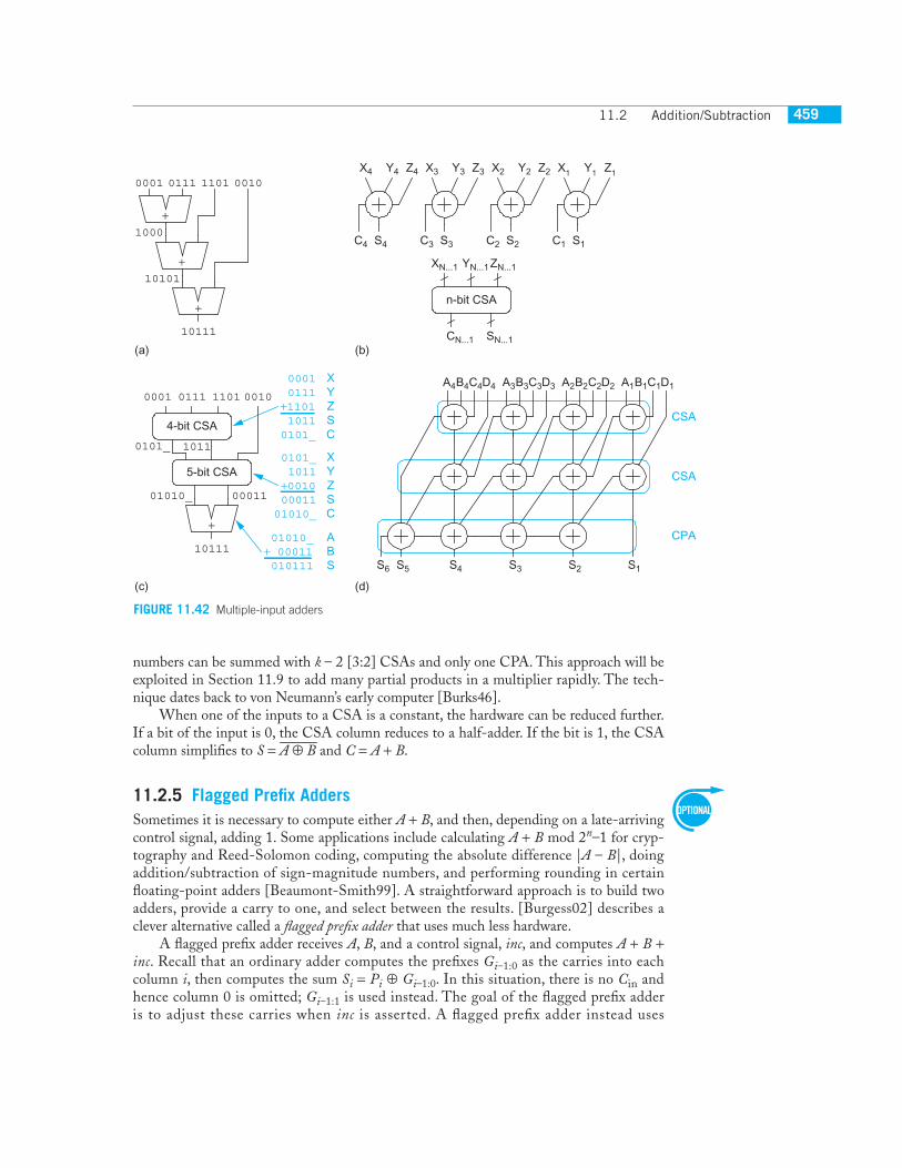
11.2.4 Multiple-Input AdditionThe most obvious method of adding k N-bit words is with k – 1 cascaded CPAs as illus-trated in Figure 11.42(a) for 0001 + 0111 + 1101 + 0010. This approach consumes a largeamount of hardware and is slow. A better technique is to note that a full adder sums threeinputs of unit weight and produces a sum output of unit weight and a carry output of dou-ble weight. If N full adders are used in parallel, they can accept three N-bit input wordsXN…1, YN…1, and ZN…1, and produce two N-bit output words SN…1 and CN…1, satisfyingX + Y + Z = S + 2C, as shown in Figure 11.42(b). The results correspond to the sums andcarries-out of each adder. This is called carry-save redundant format because the carry out-puts are preserved rather than propagated along the adder. The full adders in this applica-tion are sometimes called [3:2] carry-save adder (CSA) because they accept three inputsand produce two outputs in carry-save form. When the carry word C is shifted left by oneposition (because it has double weight) and added to the sum word S with an ordinaryCPA, the result is X + Y + Z. Alternatively, a fourth input word can be added to the carry-save redundant result with another row of CSAs, again resulting in a carry-save redundantresult. Such carry-save addition of four numbers is illustrated in Figure 11.42(c), wherethe underscores in the carry outputs serve as reminders that the carries must be shifted leftone column on account of their greater weight.
The critical path through a [3:2] adder is for the sum computation, which involvesone 3-input XOR, or two levels of XOR2. This is much faster than a CPA. In general, k
A B A B− = + + 1
0
1
2
3
4
5
6
0 20 40 60 80 100
32-bit64-bit
Prefix Tree
Carry Lookahead
Carry Select
Ripple Carry
Delay (FO4)
Are
a(Mλ2
)
FIGURE 11.40 Area vs. delay of synthesized adders
+
BN...1AN...1
SN...1 = A – B
1
(N)
(a)
+
BN...1AN...1
SN...1 A B
(N)
(b)
Sub/Add
+–=
FIGURE 11.41 Subtracters
11.2 Addition/Subtraction 459
numbers can be summed with k – 2 [3:2] CSAs and only one CPA. This approach will beexploited in Section 11.9 to add many partial products in a multiplier rapidly. The tech-nique dates back to von Neumann’s early computer [Burks46].
When one of the inputs to a CSA is a constant, the hardware can be reduced further.If a bit of the input is 0, the CSA column reduces to a half-adder. If the bit is 1, the CSAcolumn simplifies to S = A ⊕ B and C = A + B.
11.2.5 Flagged Prefix AddersSometimes it is necessary to compute either A + B, and then, depending on a late-arrivingcontrol signal, adding 1. Some applications include calculating A + B mod 2n–1 for cryp-tography and Reed-Solomon coding, computing the absolute difference |A – B|, doingaddition/subtraction of sign-magnitude numbers, and performing rounding in certainfloating-point adders [Beaumont-Smith99]. A straightforward approach is to build twoadders, provide a carry to one, and select between the results. [Burgess02] describes aclever alternative called a flagged prefix adder that uses much less hardware.
A flagged prefix adder receives A, B, and a control signal, inc, and computes A + B +inc. Recall that an ordinary adder computes the prefixes Gi–1:0 as the carries into eachcolumn i, then computes the sum Si = Pi ⊕ Gi–1:0. In this situation, there is no Cin andhence column 0 is omitted; Gi–1:1 is used instead. The goal of the flagged prefix adderis to adjust these carries when inc is asserted. A flagged prefix adder instead uses
+
(a)
(c) (d)
(b)
+
0001 0111
1000
+
1101 0010
10101
10111
Z4Y4X4
S4C4
Z3Y3X3
S3 C3
Z2Y2X2
S2C2
Z1Y1X1
S1C1
XN...1 YN...1 ZN...1
SN...1CN...1
n-bit CSA
4-bit CSA
5-bit CSA
0001 0111 1101 0010
+
10110101_
01010_ 00011
0001 0111+1101 10110101_
XYZSC
0101_ 1011 +0010 0001101010_
XYZSC
01010_+ 00011 010111
ABS
10111
A1B1C1D1A2B2C2D2A3B3C3D3A4B4C4D4
S1S2S3S4S5S6
CSA
CSA
CPA
FIGURE 11.42 Multiple-input adders

Chapter 11 Datapath Subsystems460
G ′i–1:1 = Gi–1:1 + Pi–1:1 · inc. Thus, if inc is true, it generates a carry into all of the low orderbits whose group propagate signals are TRUE. The modified prefixes, G ′i–1:1, are calledflags. The sums are computed in the same way with an XOR gate: Si = Pi ⊕ G ′i–1:1.
To produce these flags, the flagged prefix adder uses one more row of gray cells. Thisrequires that the former bottom row of gray cells be converted to black cells to produce thegroup propagate signals. Figure 11.43 shows a flagged prefix Kogge-Stone adder. The newrow, shown in blue, is appended to perform the late increment. Column 0 is eliminatedbecause there is no Cin, but column 16 is provided because applications of flagged adderswill need the generate and propagate signals spanning the entire n bits.
11.2.5.1 Modulo 2n – 1 Addition To compute A + B mod 2n – 1 for unsigned operands,an adder should first compute A + B. If the sum is greater than or equal to 2n – 1, the resultshould be incremented and truncated back to n bits. Gn:1 is TRUE if the adder will over-flow; i.e., the result is greater than 2n – 1. Pn:1 is TRUE if all columns propagate, whichonly occurs when the sum equals 2n – 1. Hence, modular addition can done with a flaggedprefix adder using inc = Gn:1 + Pn:1.
Compared to ordinary addition, modular addition requires one more row of blackcells, an OR gate to compute inc, and a buffer to drive inc across all n bits.
11.2.5.2 Absolute Difference |A – B| is called the absolute difference and is commonlyused in applications such as video compression. The most straightforward approach is tocompute both A – B and B – A, then select the positive result. A more efficient techniqueis to compute A + B and look at the sign, indicated by Gn:1. If the result is negative, itshould be inverted to obtain B – A. If the result is positive, it should be incremented toobtain A – B.
All of these operations can be performed using a flagged prefix adder enhanced toinvert the result conditionally. Modify the sum logic to calculate Si = (Pi ⊕ inv) ⊕ G ′i–1:1.Choose inv = Gn:1 and inc = Gn:1.
Compared to ordinary addition, absolute difference requires a bank of inverters toobtain B, one more row of black cells, buffers to drive inv and inc across all n bits, and arow of XORs to invert the result conditionally. Note that (Pi ⊕ inv) can be precomputedso this does not affect the critical path.
11.2.5.3 Sign-Magnitude Arithmetic Addition of sign-magnitude numbers involvesexamining the signs of the operands. If the signs agree, the magnitudes are added and the
2:13:24:35:46:57:68:79:810:911:1012:1113:1214:13
3:14:15:26:37:48:59:610:711:812:913:1014:11
5:16:17:18:19:210:311:412:513:614:7
15:1 14:1 13:1 12:1 11:1 10:1 9:1 8:1 7:1 6:1 5:1 4:1 3:1 2:1 1:1
inc
12345678910111213141516
15:1416:15
15:1216:13
15:816:9
16:1 9:110:111:112:113:114:115:1
P,Gi:1
G'i:1
FIGURE 11.43 Flagged prefix Kogge-Stone adder

11.3 One/Zero Detectors 461
sign is unchanged. If the signs differ, the absolute difference of the magnitudes must becomputed. This can be done using the flagged carry adder described in the previous sec-tion. The sign of the result is sign(A) ⊕ Gn:1.
Subtraction is identical except that the sign of B is first flipped.
11.3 One/Zero DetectorsDetecting all ones or zeros on wide N-bit words requires large fan-in AND or NOR gates.Recall that by DeMorgan’s law, AND, OR, NAND, and NOR are fundamentally thesame operation except for possible inversions of the inputs and/or outputs. You can build atree of AND gates, as shown in Figure 11.44(a). Here, alternate NAND and NOR gateshave been used. The path has log N stages. In general, the minimum logical effort isachieved with a tree alternating NAND gates and inverters and the path logical effort is
(11.24)
A rough estimate of the path delay driving a path electrical effort of H using staticCMOS gates is
(11.25)
where tFO4 is the fanout-of-4 inverter delay.
G N N NN
and ( ) =⎛⎝⎜
⎞⎠⎟
= =43
22
43 0 415
loglog .
D F t H N tFO FO≈ ( ) = +( )log log . log4 4 4 4 40 415
(a)
A0
A1
A2
A3
A4
A5
A6
A7
allones
allones
(b)
A0
A1
A2
A3
A4
A5
A6
A7
A0
A1
A2
A3
(c)
allzerosA0 A1 A2 A3
allzeros
FIGURE 11.44 One/zero detectors

Chapter 11 Datapath Subsystems462
If the word being checked has a natural skew in the arrival time of the bits (such as atthe output of a ripple adder), the designer might consider an asymmetric design thatfavors the late-arriving inputs, as shown in Figure 11.44(b). Here, the delay from the latestbit A7 is a single gate.
Another fast detector uses a pseudo-nMOS or dynamic NOR structure to performthe “wired-OR,” as shown in Figure 11.44(c). This works well for words up to about 16bits; for larger words, the gates can be split into 8–16-bit chunks to reduce the parasiticdelay and avoid problems with subthreshold leakage.
11.4 Comparators
11.4.1 Magnitude ComparatorA magnitude comparator determines the larger of two binary numbers. To compare twounsigned numbers A and B, compute B – A = B + A + 1. If there is a carry-out, A ≤ B;
otherwise, A > B. A zero detector indicates that the numbers are equal. Figure11.45 shows a 4-bit unsigned comparator built from a carry-ripple adder andtwo’s complementer. The relative magnitude is determined from the carry-out(C) and zero (Z) signals according to Table 11.4. For wider inputs, any of thefaster adder architectures can be used.
Comparing signed two’s complement numbers is slightly more complicatedbecause of the possibility of overflow when subtracting two numbers with dif-ferent signs. Instead of simply examining the carry-out, we must determine ifthe result is negative (N, indicated by the most significant bit of the result) andif it overflows the range of possible signed numbers. The overflow signal V istrue if the inputs had different signs (most significant bits) and the output signis different from the sign of B. The actual sign of the difference B – A isS = N ⊕ V because overflow flips the sign. If this corrected sign is negative(S = 1), we know A > B. Again, the other relations can be derived from the cor-rected sign and the Z signal.
11.4.2 Equality ComparatorAn equality comparator determines if (A = B). This can be done more simply and rapidlywith XNOR gates and a ones detector, as shown in Figure 11.46.
TABLE 11.4 Magnitude comparison
Relation Unsigned Comparison Signed Comparison
A = B Z Z
A ≠ B Z Z
A < B C · Z S · Z
A > B C S
A ≤ B C S
A ≥ B C + Z S + Z
A0
B0
A1
B1
A2
B2
A3
B3
A = BZ
C
A − B
NA − B>
<
FIGURE 11.45 Unsigned magnitude comparator

11.5 Counters 463
11.4.3 K = A + B ComparatorSometimes it is necessary to determine if (A + B = K ). For example, the sum-addressed memory [Heald98] described in Section 12.2.2.4 contains a decoderthat must match against the sum of two numbers, such as a register base addressand an immediate offset. Remarkably, this comparison can be done faster thancomputing A + B because no carry propagation is necessary. The key is that if youknow A and B, you also know what the carry into each bit must be if K = A + B[Cortadella92]. Therefore, you only need to check adjacent pairs of bits to verifythat the previous bit produces the carry required by the current bit, and then use aones detector to check that the condition is true for all N pairs. Specifically, if K =A + B, Table 11.5 lists what the carry-in ci – 1 must have been for this to be trueand what the carry-out ci will be for each bit position i.
From this table, you can see that the required ci–1 for bit i is
(11.26)
and the ci – 1 produced by bit i – 1 is
(11.27)
Figure 11.47 shows one bitslice of a circuit to perform this operation. The XNORgate is used to make sure that the required carry matches the produced carry at each bitposition; then the AND gate checks that the condition is satisfied for all bits.
11.5 CountersTwo commonly used types of counters are binary counters and linear-feedback shift registers.An N-bit binary counter sequences through 2N outputs in binary order. Simple designshave a minimum cycle time that increases with N, but faster designs operate in constanttime. An N-bit linear-feedback shift register sequences through up to 2N – 1 outputs inpseudo-random order. It has a short minimum cycle time independent of N, so it is usefulfor extremely fast counters as well as pseudo-random number generation.
TABLE 11.5 Required and generated carries if K = A + B
Ai Bi Ki ci–1(required)
ci(produced)
0 0 0 0 00 0 1 1 00 1 0 1 10 1 1 0 01 0 0 1 11 0 1 0 01 1 0 0 11 1 1 1 1
c A B Ki i i i− = ⊕ ⊕1
c A B K A Bi i i i i i− − − − − −= ⊕( ) +1 1 1 1 1 1·
A[0]B[0]
A = B
A[1]B[1]
A[2]B[2]
A[3]B[3]
FIGURE 11.46 Equality comparator

Chapter 11 Datapath Subsystems464
Some of the common features of counters include the following:
� Resettable: counter value is reset to 0 when RESET is asserted (essential for testing)� Loadable: counter value is loaded with N-bit value when LOAD is asserted� Enabled: counter counts only on clock cycles when EN is asserted� Reversible: counter increments or decrements based on UP/DOWN input� Terminal Count: TC output asserted when counter overflows (when counting up)
or underflows (when counting down)
In general, divide-by-M counters (M < 2N) can be built using an ordinary N-bitcounter and circuitry to reset the counter upon reaching M. M can be a programmableinput if an equality comparator is used. Alternatively, a loadable counter can be used torestart at N – M whenever TC indicates that the counter overflowed.
11.5.1 Binary CountersThe simplest binary counter is the asynchronous ripple-carry counter, as shown in Figure11.48. It is composed of N registers connected in toggle configuration, where the fallingtransition of each register clocks the subsequent register. Therefore, the delay can be quitelong. It has no reset signal, making it difficult to test. In general, asynchronous circuitsintroduce a whole assortment of problems, so the ripple-carry counter is shown mainly forhistorical interest and is not recommended for commercial designs.
A general synchronous up/down counter is shown in Figure 11.49(a). It uses a resettableregister and full adder for each bit position. The cycle time is limited by the ripple-carrydelay. While a faster adder could be used, the next section describes a better way to buildfast counters. If only an up counter (also called an incrementer) is required, the full adderdegenerates into a half adder, as shown in Figure 11.49(b). Including an input multiplexerallows the counter to load an initialization value. A clock enable is also often provided toeach register for conditional counting. The terminal count (TC) output indicates that thecounter has overflowed or underflowed. Figure 11.50 shows a fully featured resettableloadable enabled synchronous up/down counter.
clk
Q0
Q1
Q2
Q3
FIGURE 11.48 Asynchronous ripple-carry counter
Ki
AiBi
ci (Produced)
ci − 1
Equal
ci - 1
(Required)
(Produced)
FIGURE 11.47 A + B = K comparator

11.5 Counters 465
11.5.2 Fast Binary CountersThe speed of the counter in Figure 11.49 is limited by the adder. This can be overcome bydividing the counter into two or more segments [Ercegovac89]. For example, a 32-bitcounter could be constructed from a 4-bit prescalar counter and a 28-bit counter, as shownin Figure 11.51. The TC output of the prescalar enables counting on the more significantsegment. Now, the cycle time is limited only by the prescalar speed because the 28-bitadder has 24 cycles to produce a result. By using more segments, a counter of arbitrarylength can run at the speed of a 1- or 2-bit counter.
Prescaling does not suffice for up/down counters because the more significant seg-ment may have only a single cycle to respond when the counter changes direction. To solvethis, a shadow register can be used on the more significant segments to hold the previousvalue that should be used when the direction changes [Stan98]. Figure 11.52 shows themore significant segment for a fast up/down counter. On reset (not shown in the figure),the dir register is set to 0, Q to 0, and shadow to –1. When UP/DOWN changes, swap is
FIGURE 11.51 Fast binary counter
TC
clk
TC
clk
EN
TC
Q3:0 Q31:4
Least SignificantSegment
(prescalar)
Most SignificantSegment
4-Bit
Counter
28-Bit
Counter
Q0
Q1
Q2
clk
Q3
down/up
TC
r
r
r
r
reset
(a)
clkTC
r
r
r
r
reset
(b)
Q0
Q1
Q2
Q3
FIGURE 11.49 Synchronous counters
+ 0
1
load
D
Q
clk
TC
down/up
reseten
FIGURE 11.50 Synchronous up/down counter with reset, load, and enable
en en
en
+ 0
1
Q
shadow
en
clk clk
clkswap
dir
en
down/up
FIGURE 11.52 Fast binary up/down counter (most significant segment)
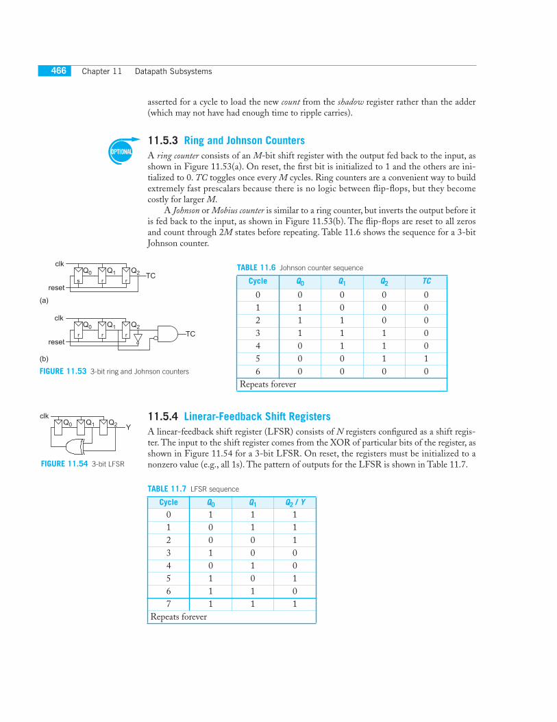
Chapter 11 Datapath Subsystems466
asserted for a cycle to load the new count from the shadow register rather than the adder(which may not have had enough time to ripple carries).
11.5.3 Ring and Johnson CountersA ring counter consists of an M-bit shift register with the output fed back to the input, asshown in Figure 11.53(a). On reset, the first bit is initialized to 1 and the others are ini-tialized to 0. TC toggles once every M cycles. Ring counters are a convenient way to buildextremely fast prescalars because there is no logic between flip-flops, but they becomecostly for larger M.
A Johnson or Mobius counter is similar to a ring counter, but inverts the output before itis fed back to the input, as shown in Figure 11.53(b). The flip-flops are reset to all zerosand count through 2M states before repeating. Table 11.6 shows the sequence for a 3-bitJohnson counter.
11.5.4 Linerar-Feedback Shift RegistersA linear-feedback shift register (LFSR) consists of N registers configured as a shift regis-ter. The input to the shift register comes from the XOR of particular bits of the register, asshown in Figure 11.54 for a 3-bit LFSR. On reset, the registers must be initialized to anonzero value (e.g., all 1s). The pattern of outputs for the LFSR is shown in Table 11.7.
TABLE 11.6 Johnson counter sequence
Cycle Q0 Q1 Q2 TC
0 0 0 0 01 1 0 0 02 1 1 0 03 1 1 1 04 0 1 1 05 0 0 1 16 0 0 0 0
Repeats forever
TABLE 11.7 LFSR sequence
Cycle Q0 Q1 Q2 / Y
0 1 1 11 0 1 12 0 0 13 1 0 04 0 1 05 1 0 16 1 1 07 1 1 1
Repeats forever
s r r
clk
reset
TCQ0 Q1 Q2
Q0 Q1 Q2
r r r
clk
resetTC
(a)
(b)
FIGURE 11.53 3-bit ring and Johnson counters
Q0 Q1 Q2 Y
clk
FIGURE 11.54 3-bit LFSR

11.5 Counters 467
This LFSR is an example of a maximal-length shift register because its outputsequences through all 2n – 1 combinations (excluding all 0s). The inputs fed to the XORare called the tap sequence and are often specified with a characteristic polynomial. For exam-ple, this 3-bit LFSR has the characteristic polynomial 1 + x 2 + x3 because the taps comeafter the second and third registers.
The output Y follows the 7-bit sequence [1110010]. This is an example of a pseudo-random bit sequence (PRBS). LFSRs are used for high-speed counters and pseudo-randomnumber generators. The pseudo-random sequences are handy for built-in self-test andbit-error-rate testing in communications links. They are also used in many spread-spectrum communications systems such as GPS and CDMA where their correlationproperties make other users look like uncorrelated noise.
Table 11.8 lists characteristic polynomials for some commonly used maximal-lengthLFSRs. For certain lengths, N, more than two taps may be required. For many values ofN, there are multiple polynomials resulting in different maximal-length LFSRs. Observethat the cycle time is set by the register and a small number of XOR delays. [Golomb81]offers the definitive treatment on linear-feedback shift registers.
Example 11.1
Sketch an 8-bit linear-feedback shift register.How long is the pseudo-random bit sequencethat it produces?
SOLUTION: Figure 11.55 shows an 8-bit LFSRusing the four taps after the 1st, 6th, 7th, and 8thbits, as given in Table 11.7. It produces a sequenceof 28 – 1 = 255 bits before repeating.
TABLE 11.8 Characteristic polynomials
N Polynomial
3 1 + x2 + x3
4 1 + x3 + x4
5 1 + x3 + x5
6 1 + x5 + x6
7 1 + x6 + x7
8 1 + x1 + x6 + x7 + x8
9 1 + x5 + x9
15 1 + x14 + x15
16 1 + x4 + x13 + x15 + x16
23 1 + x18 + x23
24 1 + x17 + x22 + x23 + x24
31 1 + x28 + x31
32 1 + x10 + x30 + x31 + x32
Y
clkQ0 Q1 Q2 Q3 Q4 Q5 Q6 Q7
FIGURE 11.55 8-bit LFSR

Chapter 11 Datapath Subsystems468
11.6 Boolean Logical OperationsBoolean logical operations are easily accomplished using a multiplexer-based circuit, asshown in Figure 11.56. Table 11.9 shows how the inputs are assigned to perform differentlogical functions. By providing different P values, the unit can perform other operationssuch as XNOR(A, B) or NOT(A). An Arithmetic Logic Unit (ALU) requires both arith-metic (add, subtract) and Boolean logical operations.
11.7 CodingError-detecting and error-correcting codes are used to increase system reliability. Memoryarrays are particularly susceptible to soft errors caused by alpha particles or cosmic raysflipping a bit. Such errors can be detected or even corrected by adding a few extra check bitsto each word in the array. Codes are also used to reduce the bit error rate in communica-tion links.
The simplest form of error-detecting code is parity, which detects single-bit errors.More elaborate error-correcting codes (ECC) are capable of single-error correcting anddouble-error detecting (SEC-DED). Gray codes are another useful alternative to thestandard binary codes. All of the codes are heavily based on the XOR function, so we willexamine a variety of CMOS XOR designs.
11.7.1 ParityA parity bit can be added to an N-bit word to indicate whether the number of 1s in theword is even or odd. In even parity, the extra bit is the XOR of the other N bits, whichensures the (N + 1)-bit coded word has an even number of 1s:
(11.28)
Figure 11.57 shows a conventional implementation. Multi-input XOR gates can alsobe used.
11.7.2 Error-Correcting CodesThe Hamming distance [Hamming50] between a pair of binary numbers is the number ofbits that differ between the two numbers. A single-bit error transforms a data word intoanother word separated by a Hamming distance of 1. Error-correcting codes add checkbits to the data word so that the minimum Hamming distance between valid wordsincreases. Parity is an example of a code with a single check bit and a Hamming distance
TABLE 11.9 Functions implemented by Boolean unit
Operation P0 P1 P2 P3
AND(A, B) 0 0 0 1OR(A, B) 0 1 1 1XOR(A, B) 0 1 1 0NAND(A, B) 1 1 1 0NOR(A, B) 1 0 0 0
A A A A An n= = ⊕ ⊕ ⊕ ⊕ −PARITY 0 1 2 1...
Y
0P0
1
0
1
0
1
B A
P1
P2
P3
FIGURE 11.56 Boolean logical unit
Y
A7A6
A5A4
A3A2
A1A0
FIGURE 11.57 8-bit parity generator

11.7 Coding 469
of 2 between valid words, so that single-bit errors lead to invalid words and hence aredetectable. If more check bits are added so that the minimum distance between validwords is 3, a single-bit error can be corrected because there will be only one valid wordwithin a distance of 1. If the minimum distance between valid words is 4, a single-bit errorcan be corrected and an error corrupting two bits can be detected (but not corrected). Ifthe probability of bit errors is low and uncorrelated from one bit to another, such singleerror-correcting, double error-detecting (SEC-DED) codes greatly reduce the overallerror rate of the system. Larger Hamming distances improve the error rate further at theexpense of more check bits.
In general, you can construct a distance-3 Hamming code of length up to 2c – 1 withc check bits and N = 2c – c – 1 data bits using a simple procedure [Wakerly00]. If the bitsare numbered from 1 to 2c – 1, each bit in a position that is a power of 2 serves as a checkbit. The value of the check bit is chosen to obtain even parity for all bits with a 1 in thesame position as the check bit, as illustrated in Figure 11.58(a) for a 7-bit code with 4 databits and 3 check bits. The bits are traditionally reorganized into contiguous data and checkbits, as shown in Figure 11.58(b). The structure is called a parity-check matrix and eachcheck bit can be computed as the XOR of the highlighted data bits:
(11.29)
The error-correcting decoder examines the check bits. If they all have even parity, theword is considered to be correct. If one or more groups have odd parity, an error hasoccurred. The pattern of check bits that have the wrong parity is called the syndrome andcorresponds to the bit position that is incorrect. The decoder must flip this bit to recoverthe correct result.
Example 11.2
Suppose the data value 1001 were to be transmitted using a distance-3 Hamming code.What are the check bits? If the data bits were garbled into 1101 during transmission,explain what the syndrome would be and how the data would be corrected.
SOLUTION: According to EQ (11.29), the check bits should be 100, corresponding to atransmitted word of 1001100. The received word is 1101100. The syndrome is 110,
C D D D
C D D D
C D D D
0 3 1 0
1 3 2 0
2 3 2 1
= ⊕ ⊕
= ⊕ ⊕
= ⊕ ⊕
1001
2010
3011
4100
5101
6110
7111
Bit Position
Che
ck G
roup
Che
ck G
roup
1
2
4
(a) (b)
1001
2010
3011
4100
5101
6110
7111
Bit Position
1
2
4
Check BitsData BitsCheck Bits
D3 D2 C2 C1 C0D1 D0
FIGURE 11.58 Parity-check matrix

Chapter 11 Datapath Subsystems470
i.e., odd parity on check bits C2 and C1, which indicates an error in bit position 110 =6. This position is flipped to produce a corrected word of 1001100 and the check bitsare discarded, leaving the proper data value of 1001.
A SEC-DED distance-4 Hamming code can be constructed from a distance-3 codeby adding one more parity bit for the entire word. If there is a single-bit error, parity willfail and the check bits will indicate how to correct the data. If there is a double-bit error,the check bits will indicate an error, but parity will pass, indicating a detectable but uncor-rectable double-bit error.
The parity check matrix determines the number of XORs required in the encodingand decoding logic. A SEC-DED Hamming code for a 64-bit data word has 8 check bits.It requires 296 XOR gates. The parity logic for the entire word has 72 inputs. The HsiaoSEC-DED achieves the same function with the same number of data and check bits but isingeniously designed to minimize the cost, using only 216 XOR gates and parity logicwith a maximum of 27 inputs. [Hsiao70] shows parity-check matrices for 16, 32, and 64-bit data words with 6, 7, and 8 check bits.
As the data length and allowable decoder complexity increase, other codes becomeefficient. These include Reed-Solomon, BCH, and Turbo codes. [Lin83, Sweeney02,Sklar01, Fujiwara06] and many other texts provide extensive information on a variety oferror-correcting codes.
11.7.3 Gray CodesThe Gray codes, named for Frank Gray, who patented their use on shaft encoders[Gray53], have a useful property that consecutive numbers differ in only one bit position.While there are many possible Gray codes, one of the simplest is the binary-reflected Graycode that is generated by starting with all bits 0 and successively flipping the right-most bitthat produces a new string. Table 11.10 compares 3-bit binary and binary-reflected Graycodes. Finite state machines that typically move through consecutive states can save powerby Gray-coding the states to reduce the number of transitions. When a counter value mustbe synchronized across clock domains, it can be Gray-coded so that the synchronizer iscertain to receive either the current or previous value because only one bit changes eachcycle.
Converting between N-bit binary B and binary-reflected Gray code G representationsis remarkably simple.
TABLE 11.10 3-bit Gray code
Number Binary Gray Code
0 000 0001 001 0012 010 0113 011 0104 100 1105 101 1116 110 1017 111 100

11.7 Coding 471
(11.30)
11.7.4 XOR/XNOR Circuit FormsOne of the chronic difficulties in CMOS circuit design is to construct a fast, compact,low-power XOR or XNOR gate. Figure 11.59 shows a number of common static single-rail 2-input XOR designs; XNOR designs are similar. Figure 11.59(a) and Figure11.59(b) show gate-level implementations; the first is cute, but the second is slightly moreefficient. Figure 11.59(c) shows a complementary CMOS gate. Figure 11.59(d) improvesthe gate by optimizing out two contacts and is a commonly used standard cell design. Fig-ure 11.59(e) shows a transmission gate design. Figure 11.59(f ) is the 6-transistor “invert-ible inverter” design. When A is 0, the transmission gate turns on and B is passed to theoutput. When A is 1, the A input powers a pair of transistors that invert B. It is compact,but nonrestoring. Some switch-level simulators such as IRSIM cannot handle this uncon-ventional design. Figure 11.59(g) [Wang94] is a compact and fast 4-transistor pass-gatedesign, but does not swing rail to rail.
XOR gates with 3 or 4 inputs can be more compact, although not necessarily fasterthan a cascade of 2-input gates. Figure 11.60(a) is a 4-input static CMOS XOR[Griffin83] and Figure 11.60(b) is a 4-input CPL XOR/XNOR, while Figure 9.20(c)showed a 4-input CVSL XOR/XNOR. Observe that the true and complementary treesshare most of the transistors. As mentioned in Chapter 9, CPL does not perform well atlow voltage.
Dynamic XORs pose a problem because both true and complementary inputs arerequired, violating the monotonicity rule. The common solutions mentioned in Section11.2.2.11 are to either push the XOR to the end of a chain of domino logic and build it
Binary Binary→ →= =
=− − − −
+
Gray Gray
G B B G
G BN N N N
i i
1 1 1 1
1 ⊕⊕ = ⊕ − > ≥+B B B G N ii i i i1 1 0
AY
B
A
B
A ABB
AA
BB
AY
B
A
B
A
A
B
B
AA
BB
A
BA
B
Y
AA
YA
A
B B
AB
Y
(a) (b)
BA Y
(c)
A
A
A
B
B
Y
AA
BB
(d) (e) (f) (g)
FIGURE 11.59 Static 2-input XOR designs

Chapter 11 Datapath Subsystems472
with static CMOS or to construct a dual-rail domino structure. A dual-rail domino2-input XOR was shown in Figure 9.30(c).
11.8 Shifters Shifts can either be performed by a constant or variable amount. Constant shifts are trivialin hardware, requiring only wires. They are also an efficient way to perform multiplicationor division by powers of two. A variable shifter takes an N-bit input, A, a shift amount, k,and control signals indicating the shift type and direction. It produces an N-bit output, Y.There are three common types of variable shifts, each of which can be to the left or right:
� Rotate: Rotate numbers in a circle such that empty spots are filled with bits shifted off the other end
○ Example: 1011 ROR 1 = 1101; 1011 ROL 1 = 0111� Logical shift: Shift the number to the left or right and fills empty spots with zeros.
○ Example: 1011 LSR 1 = 0101; 1011 LSL 1 = 0110 � Arithmetic shift: Same as logical shifter, but on right shifts fills the most significant
bits with copies of the sign bit (to properly sign, extend two’s complement num-bers when using right shift by k for division by 2k).
○ Example: 1011 ASR 1 = 1101; 1011 ASL 1 = 0110
Conceptually, rotation involves an array of N N-input multiplexers to select each ofthe outputs from each of the possible input positions. This is called an array shifter. Thearray shifter requires a decoder to produce the 1-of-N-hot shift amount. In practice, mul-tiplexers with more than 4–8 inputs have excessive parasitic capacitance, so they are fasterto construct from logv N levels of v-input multiplexers. This is called a logarithmic shifter.For example, in a radix-2 logarithmic shifter, the first level shifts by N/2, the second byN/4, and so forth until the final level shifts by 1. In a logarithmic shifter, no decoder isnecessary. The CMOS transmission gate multiplexer of Figure 9.47 is especially well-suited to logarithmic shifters because the hefty wire capacitance is driven directly by aninverter rather than through a pair of series transistors. 4:1 or 8:1 transmission gate multi-plexers reduce the number of levels by a factor of 2 or 3 at the expense of more wiring and
YA
B B
C C
D
A
B B
C C
D
D
C C
B B
A
D
C C
B B
A
(a) (b)
D
D
L
L Y
Y
C
C
C
C
B
B
B
B A
A
A
A
FIGURE 11.60 4-input XOR designs

11.8 Shifters 473
fanout. Pairs or triplets of the shift amount are decoded to drive one-hot mux selects ateach level. [Tharakan92] describes a domino logarithmic shifter using 3:1 multiplexers toreduce the number of logic levels.
A left rotate by k bits is equivalent to a right rotate by N – k bits. Computing N – krequires a subtracter in the critical path. Taking advantage of two’s complement arithmeticand the fact that rotation is cyclic modulo N, N – k = N + k + 1 = k + 1. Thus, the leftrotate can be performed by preshifting right by 1, then doing a right rotate by the comple-mented shift amount.
Logical and arithmetic shifts are similar to rotates, but must replace bits at one end orthe other with a kill value (either 0 or the sign bit). The two major shifter architectures arefunnel shifters and barrel shifters. In a funnel shifter, the kill values are incorporated at thebeginning, while in a barrel shifter, the kill values are chosen at the end. Each of thesearchitectures is described below. Both barrel and funnel shifters can use array or logarith-mic implementations. [Huntzicker08] examines the energy-delay trade-offs in staticshifters. For general-purpose shifting, both architectures are comparable in energy anddelay. Given typical parasitics capacitances, the theory of Logical Effort shows that loga-rithmic structure using 4:1 multiplexers is most efficient. If only shift operations(but not rotates) are required, the funnel architecture is simpler, while if onlyrotates (but not shifts) are required, the barrel is simpler.
11.8.1 Funnel ShifterThe funnel shifter creates a 2N – 1-bit input word Z from A and/or the kill val-ues, then selects an N-bit field from this input word, as shown in Figure 11.61. Itgets its name from the way the wide word funnels down to a narrower one. Table11.11 shows how Z is formed for each type of shift. Z incorporates the 1-bit pre-shift for left shifts.
The simplest funnel shifter design consists of an array of N N-inputmultiplexers accepting 1-of-N-hot select signals (one multiplexer for eachoutput bit). Such an array shifter is shown in Figure 11.62 using nMOS passtransistors for a 4-bit shifter. The shift amount is conditionally inverted anddecoded into select signals that are fed vertically across the array. The outputsare taken horizontally. Each row of transistors attached to an output formsone of the multiplexers. The 2N – 1 inputs run diagonally to the appropriatemux inputs. Figure 11.63 shows a stick diagram for one of the N 2 transistorsin the array. nMOS pass transistors suffer a threshold drop, but the problemcan be solved by precharging the outputs (done in the Alpha 21164[Gronowski96]) or by using full CMOS transmission gates.
TABLE 11.11 Funnel shifter source generator
Shift Type Z2N – 2:N ZN – 1 ZN – 2:0 Offset
Logical Right AN–2:0 AN–1 AN–2:0 k
Arithmetic Right 0 AN–1 AN–2:0 k
Rotate Right sign AN–1 AN–2:0 k
Logical/Arithmetic Left AN–1:1 A0 AN–1:1 k
Rotate Left AN–1:1 A0 0 k
Z
OffsetOffset + N − 1
02N − 2
Y
0N − 1
FIGURE 11.61 Funnel shifter function
k[1:0]
Left Inverters & Decoder
Y3
s3 s2 s1 s0
Y2
Y1
Y0
Z0Z1Z2Z3Z4
Z5
Z6
FIGURE 11.62 4-bit array funnel shifter

Chapter 11 Datapath Subsystems474
The array shifter works well for small shifters in transistor-level designs, but has highparasitic capacitance in larger shifters, leading to excessive delay and energy. Moreover,array shifters are not amenable to standard cell designs. Figure 11.64 shows a 4-bit loga-rithmic shifter based on multiple levels of 2:1 multiplexers (which, of course, can be trans-mission gates) [Lim72]. The XOR gates on the control inputs conditionally invert theshift amount for left shifts.
Figure 11.65 shows a 32-bit funnel shifter using a 4:1 multiplexer followed by an 8:1multiplexer [Huntzicker08]. The source generator selects the 63-bit Z. The first stage per-forms a coarse shift right by 0, 8, 16, or 24 bits. The second stage performs a fine shiftright by 0–7 bits. The mux decode block conditionally inverts k for left shifts, computesthe 1-hot selects, and buffers them to drive the wide multiplexers.
Conceptually, the source generator consists of a 2N – 1-bit 5:1 multiplexer controlled bythe shift type and direction. Figure 11.66 shows how the source generator logic can be sim-plified. The horizontal control lines need to be buffered to drive the high fanout and they areon the critical path. Even if they are available early, the sign bit is still critical. If only certaintypes of shifts or rotates are supported, the logic can be optimized down further.
Y
Z
ZS
FIGURE 11.63 Array funnel shifter cell stick diagram
leftZ0Z1Z2Z3
Y0
k1
k0Y1Y2Y3
Z4Z5Z6
FIGURE 11.64 4-bit logarithmic funnel shifter
Source Generator
A
32
63
39
32
Y
Z
5k
left
arithshift
4
8
4:1
8:1
Mux D
ecode
FIGURE 11.65 32-bit logarithmic funnel shifter
left
arith
shift
AN-1
AN − 2:0 AN − 1
ZN − 1
A0AN − 1:1 AN − 2:0 AN − 1:1
ZN − 2:N ZN − 2:0
(sign)left
leftshift
SignExt
RightRot
LeftRot
FIGURE 11.66 Optimized source generator logic

11.8 Shifters 475
The funnel shifter presents a layout problembecause the source generator and early stages of multi-plexers are wider than the rest of the datapath. Figure11.67 shows a floorplan in which the source generatoris folded to fit the datapath. Such folding also reduceswire lengths, saving energy. Depending on the layoutconstraints, the extra seven most significant bits of thefirst-level multiplexer may be folded into another rowor incorporated into the zipper.
11.8.2 Barrel ShifterA barrel shifter performs a right rotate operation[Davis69]. As mentioned earlier, it handles left rota-tions using the complementary shift amount. Barrelshifters can also perform shifts when suitable maskinghardware is included. Barrel shifters come in array andlogarithmic forms; we focus on logarithmic barrelshifters because they are better suited for large shifts.
Figure 11.68(a) shows a simple 4-bit barrel shifterthat performs right rotations. Notice how, unlike fun-nel shifters, barrel shifters contain long wrap-aroundwires. In a large shifter, it is beneficial to upsize orbuffer the drivers for these wires. Figure 11.68(b)shows an enhanced version that can rotate left by pre-rotating right by 1, then rotating right by k. Perform-ing logical or arithmetic shifts on a barrel shifterrequires a way to mask out the bits that are rotated offthe end of the shifter, as shown in Figure 11.68(c).
Figure 11.69 shows a 32-bit barrel shifter using a5:1 multiplexer and an 8:1 multiplexer. The first stagerotates right by 0, 1, 2, 3, or 4 bits to handle a prerotateof 1 bit and a fine rotate of up to 3 bits combined intoone stage. The second stage rotates right by 0, 4, 8, 12,16, 20, 24, or 28 bits. The critical path starts withdecoding the shift amount for the first stage. If the shiftamount is available early, the delay from A to Yimproves substantially.
While the rotation is taking place, the maskingunit generates an N-bit mask with ones where the killvalue should be inserted for right shifts. For a rightshift by m, the m most significant bits are ones. This iscalled a thermometer code and the logic to compute itis described in Section 11.10. When the rotation resultX is complete, the masking unit replaces the masked bits with the kill value. For left shifts,the mask is reversed. Figure 11.70 shows masking logic. If only certain shifts are sup-ported, the unit can be simplified, and if only rotates are supported, the masking unit canbe eliminated, saving substantial hardware, power, and delay.
31
0
38
31
31
1
0
Source Generator Bits
0-31
Source Generator Bits
32-62
mux4
mux8
0
FIGURE 11.67 Funnel shifter floorplans
left
Preshift
Mask arithmeticshift
sign
left
A3 A2 A1 A0
A3 A2 A1 A0
A3 A2 A1 A0
Y3 Y2 Y1 Y0 Y3 Y2 Y1 Y0
Y3 Y2 Y1 Y0
X3 X2 X1 X0
k0
k1
k0
k1
k0
k1
S0
S1
(a) (b)
(c)
FIGURE 11.68 Barrel shifters: (a) rotate right, (b) rotate left or right, (c) rotates and shifts

Chapter 11 Datapath Subsystems476
11.8.3 Alternative Shift FunctionsOther flavors of shifts, including shuffles, bit-reversals, interchanges, extraction, anddeposit, are sometimes required, especially for cryptographic and multimedia applications[Hilewitz04, Hilewitz07]. These are also built from appropriate combinations of multi-plexers.
11.9 MultiplicationMultiplication is less common than addition, but is still essential for microprocessors, dig-ital signal processors, and graphics engines. The most basic form of multiplication consists
of forming the product of two unsigned (positive) binary numbers. This canbe accomplished through the traditional technique taught in primary school,simplified to base 2. For example, the multiplication of two positive 6-bitbinary integers, 2510 and 3910, proceeds as shown in Figure 11.71.
M × N-bit multiplication P = Y × X can be viewed as forming N partialproducts of M bits each, and then summing the appropriately shifted partialproducts to produce an M + N-bit result P. Binary multiplication is equivalentto a logical AND operation. Therefore, generating partial products consists ofthe logical ANDing of the appropriate bits of the multiplier and multiplicand.Each column of partial products must then be added and, if necessary, anycarry values passed to the next column. We denote the multiplicand as
Y = {yM–1, yM–2, …, y1, y0} and the multiplier as X = {xN–1, xN–2, …, x1, x0}. For unsignedmultiplication, the product is given in EQ (11.31). Figure 11.72 illustrates the generation,shifting, and summing of partial products in a 6 × 6-bit multiplier.
(11.31)P y x x yjj
j
M
ii
i
N
i ji j=
⎛
⎝⎜⎜
⎞
⎠⎟⎟
⎛
⎝⎜
⎞
⎠⎟ =
=
−
=
−+∑ ∑2 2 2
0
1
0
1
jj
M
i
N
=
−
=
−
∑∑0
1
0
1
left
arithAN − 1
maskN − 2:0 XN − 1:0
YN − 1:0
(sign)
shift
Kill X
LeftShifts
RightShifts
SignExt
Reverse
FIGURE 11.70 Barrel shifter masking logic
multiplier
multiplicand
partial products
product
011001 : 2510 100111 : 3910 011001 011001 011001 000000 000000+011001001111001111 : 97510
FIGURE 11.71 Multiplication example
A
32
32
Masking
32
32
Y
5k
5
8
arith
leftshift
X
5:1
8:1
Mux D
ecode
FIGURE 11.69 32-bit logarithmic barrel shifter

11.9 Multiplication 477
Large multiplications can be more conveniently illustrated using dot diagrams. Figure11.73 shows a dot diagram for a simple 16 × 16 multiplier. Each dot represents a place-holder for a single bit that can be a 0 or 1. The partial products are represented by a hori-zontal boxed row of dots, shifted according to their weight. The multiplier bits used togenerate the partial products are shown on the right.
There are a number of techniques that can be used to perform multiplication. In gen-eral, the choice is based upon factors such as latency, throughput, energy, area, and designcomplexity. An obvious approach is to use an M + 1-bit carry-propagate adder (CPA) toadd the first two partial products, then another CPA to add the third partial product to therunning sum, and so forth. Such an approach requires N – 1 CPAs and is slow, even if afast CPA is employed. More efficient parallel approaches use some sort of array or tree offull adders to sum the partial products. We begin with a simple array for unsigned multi-pliers, and then modify the array to handle signed two’s complement numbers using theBaugh-Wooley algorithm. The number of partial products to sum can be reduced usingBooth encoding and the number of logic levels required to perform the summation can bereduced with Wallace trees. Unfortunately, Wallace trees are complex to lay out and havelong, irregular wires, so hybrid array/tree structures may be more attractive. For complete-ness, we consider a serial multiplier architecture. This was once popular when gates wererelatively expensive, but is now rarely necessary.
Multiplier
Multiplicand
PartialProducts
Productp11
x5y5 x5y4 x5y3 x5y2 x5y1 x5y0
x4y5 x4y4 x4y3 x4y2 x4y1 x4y0
x3y5 x3y4 x3y3 x3y2 x3y1 x3y0
x2y5 x2y4 x2y3 x2y2 x2y1 x2y0
x1y5 x1y4 x1y3 x1y2 x1y1 x1y0
x0y5
y5 y4 y3 y2 y1 y0
x5 x4 x3 x2 x1 x0
x0y4 x0y3 x0y2 x0y1 x0y0
p10 p9 p8 p7 p6 p5 p4 p3 p2 p1 p0
FIGURE 11.72 Partial products
Partial Products
x0
x15
Multiplier x
FIGURE 11.73 Dot diagram

Chapter 11 Datapath Subsystems478
11.9.1 Unsigned Array MultiplicationFast multipliers use carry-save adders (CSAs, see Section 11.2.4) to sum the partial prod-ucts. A CSA typically has a delay of 1.5–2 FO4 inverters independent of the width of thepartial product, while a carry-propagate adder (CPA) tends to have a delay of 4–15+ FO4inverters depending on the width, architecture, and circuit family. Figure 11.74 shows a4 × 4 array multiplier for unsigned numbers using an array of CSAs. Each cell contains a2-input AND gate that forms a partial product and a full adder (CSA) to add the partialproduct into the running sum. The first row converts the first partial product intocarry-save redundant form. Each later row uses the CSA to add the corresponding partialproduct to the carry-save redundant result of the previous row and generate a carry-saveredundant result. The least significant N output bits are available as sum outputs directlyfrom CSAs. The most significant output bits arrive in carry-save redundant form andrequire an M-bit carry-propagate adder to convert into regular binary form. In Figure11.74, the CPA is implemented as a carry-ripple adder. The array is regular in structureand uses a single type of cell, so it is easy to design and lay out. Assuming the carry outputis faster than the sum output in a CSA, the critical path through the array is marked onthe figure with a dashed line. The adder can easily be pipelined with the placement of reg-isters between rows. In practice, circuits are assigned rectangular blocks in the floorplan sothe parallelogram shape wastes space. Figure 11.75 shows the same adder squashed to fit arectangular block.
B
ASin Cin
SoutCout
BA
CinCout
Sout
Sin
CSAArray
CPA
Critical Path BA
Sout
Cout CinCout
Sout
=Cin
BA
y3
p7 p6
y2 y1 y0
x0
x1
x2
x3
p5 p4 p3 p2 p1 p0
=
FIGURE 11.74 Array multiplier

11.9 Multiplication 479
A key element of the design is a compact CSA. This not onlybenefits area but also helps performance because it leads to shortwires with low wire capacitance. An ideal CSA design has approxi-mately equal sum and carry delays because the greater of these twodelays limits performance. The mirror adder from Figure 11.4 iscommonly used for its compact layout even though the sum delayexceeds the carry delay. The sum output can be connected to thefaster carry input to partially compensate [Sutherland99, Hsu06a].
Note that the first row of CSAs adds the first partial product toa pair of 0s. This leads to a regular structure, but is inefficient. At aslight cost to regularity, the first row of CSAs can be used to add thefirst three partial products together. This reduces the number of rowsby two and correspondingly reduces the adder propagation delay. Yetanother way to improve the multiplier array performance is toreplace the bottom row with a faster CPA such as a lookahead or treeadder. In summary, the critical path of an array multiplier involvesN–2 CSAs and a CPA.
11.9.2 Two’s Complement Array MultiplicationMultiplication of two’s complement numbers at first might seemmore difficult because some partial products are negative and mustbe subtracted. Recall that the most significant bit of a two’s comple-ment number has a negative weight. Hence, the product is
In EQ (11.32), two of the partial products have negative weight and thus should besubtracted rather than added. The Baugh-Wooley [Baugh73] multiplier algorithm handlessubtraction by taking the two’s complement of the terms to be subtracted (i.e., inverting thebits and adding one). Figure 11.76 shows the partial products that must be summed. Theupper parallelogram represents the unsigned multiplication of all but the most significantbits of the inputs. The next row is a single bit corresponding to the product of the mostsignificant bits. The next two pairs of rows are the inversions of the terms to be subtracted.Each term has implicit leading and trailing zeros, which are inverted to leading and trail-ing ones. Extra ones must be added in the least significant column when taking the two’scomplement.
The multiplier delay depends on the number of partial product rows to be summed.The modified Baugh-Wooley multiplier [Hatamian86] reduces this number of partial prod-ucts by precomputing the sums of the constant ones and pushing some of the termsupward into extra columns. Figure 11.77 shows such an arrangement. The parallelogram-shaped array can again be squashed into a rectangle, as shown in Figure 11.78, giving adesign almost identical to the unsigned multiplier of Figure 11.75. The AND gates arereplaced by NAND gates in the hatched cells and 1s are added in place of 0s at two of the
P y y x xMM
jj
j
M
nN
ii
i
= − +⎛
⎝⎜⎜
⎞
⎠⎟⎟
− +−−
=
−
−−
=∑1
1
0
2
112 2 2 2
00
2
1 12
12 2 2
N
i ji j
N MM N
i Mi Mx y x y x y
−
+− −
+ −−
+
∑⎛
⎝⎜
⎞
⎠⎟
= + − −−
=
−
−+ −
=
−
=
−
=∑ ∑∑ +
⎛
⎝⎜⎜
⎞
⎠⎟⎟
1
0
2
11
0
2
0
2
2i
N
N jj N
j
M
j
M
i
x y00
2N −
∑
(11.32)
y3 y2 y1 y0
x0
x1
x2
x3
p7 p6 p5 p4
p3
p2
p1
p0
FIGURE 11.75 Rectangular array multiplier
(11.32)

Chapter 11 Datapath Subsystems480
1
1
p11
y5 y4 y3 y2 y1 y0
x5 x4 x3 x2 x1 x0
p10 p9 p8 p7 p6 p5 p4 p3 p2 p1
x5y5 x4y5 x3y5 x2y5 x1y5 x0y5
x5y4 x4y4 x4y3 x4y2 x4y1 x4y0
x5y3 x3y4 x3y3 x3y2 x3y1 x3y0
x5y2 x2y4 x2y3 x2y2 x2y1 x2y0
x5y1 x1y4 x1y3 x1y2 x1y1 x1y0
x5y0 x0y4 x0y3 x0y2 x0y1 x0y0
FIGURE 11.77 Simplified partial products for two’s complement multiplier
y3 y2 y1 y0
x0
x1
x2
x3
p7 p6 p5 p4
p3
p2
p1
p0
FIGURE 11.78 Modified Baugh-Wooley two’s comple-ment multiplier
unused inputs. The signed and unsigned arrays are so similar that a single array can be usedfor both purposes if XOR gates are used to conditionally invert some of the terms depend-ing on the mode.
11.9.3 Booth EncodingThe array multipliers in the previous sections compute the partial products in a radix-2manner; i.e., by observing one bit of the multiplier at a time. Radix 2r multipliers produce
11 11 11 1
11 11 11 1
1
1
∑∑ N − 2 M − 2
i = 0 j = 0
xi yj 2i + j
∑ M − 2
j = 0
xN − 1 yj 2j + N − 1
∑ N − 2
i = 0
xi yM − 1 2i + M − 1
xN − 1 yM −1 2M + N − 2
p11 p10 p9 p8 p7 p6 p5 p4 p3 p2 p1 p0
x5y4 x5y3 x5y2 x5y1 x5y0
x4y5 x3y5 x2y5 x1y5 x0y5
x4y4
x5y5
x4y3 x4y2 x4y1 x4y0
x3y4 x3y3 x3y2 x3y1 x3y0
x2y4 x2y3 x2y2 x2y1 x2y0
x1y4 x1y3 x1y2 x1y1 x1y0
x0y4 x0y3 x0y2 x0y1 x0y0
y5 y4 y3 y2 y1 y0
x5 x4 x3 x2 x1 x0
FIGURE 11.76 Partial products for two’s complement multiplier

11.9 Multiplication 481
N/r partial products, each of which depend on r bits of the multiplier. Fewer partial prod-ucts leads to a smaller and faster CSA array. For example, a radix-4 multiplier producesN/2 partial products. Each partial product is 0, Y, 2Y, or 3Y, depending on a pair of bits ofX. Computing 2Y is a simple shift, but 3Y is a hard multiple requiring a slow carry-propagate addition of Y + 2Y before partial product generation begins.
Booth encoding was originally proposed to accelerate serial multiplication [Booth51].Modified Booth encoding [MacSorley61] allows higher radix parallel operation without gen-erating the hard 3Y multiple by instead using negative partial products. Observe that3Y = 4Y – Y and 2Y = 4Y – 2Y. However, 4Y in a radix-4 multiplier array is equivalent to Yin the next row of the array that carries four times the weight. Hence, partial products arechosen by considering a pair of bits along with the most significant bit from the previouspair. If the most significant bit from the previous pair is true, Y must be added to the cur-rent partial product. If the most significant bit of the current pair is true, the current par-tial product is selected to be negative and the next partial product is incremented.
Table 11.12 shows how the partial products are selected, based on bits of the multi-plier. Negative partial products are generated by taking the two’s complement of themultiplicand (possibly left-shifted by one column for –2Y ). An unsigned radix-4 Booth-encoded multiplier requires partial products rather than N. Each partialproduct is M + 1 bits to accommodate the 2Y and –2Y multiples. Even though X and Y areunsigned, the partial products can be negative and must be sign extended properly. TheBooth selects will be discussed further after an example.
Example 11.3
Repeat the multiplication of P = Y × X = 0110012 × 1001112 from Fig-ure 11.71, applying Booth encoding to reduce the number of partialproducts.
SOLUTION: Figure 11.79 shows the multiplication. X is written verti-cally and the bits are used to select the four partial products. Each par-tial product is shifted two columns left of the previous one because ithas four times the weight. The upper bits are sign-extended with 1s fornegative partial products and 0s for positive partial products. The par-tial products are added to obtain the result.
TABLE 11.12 Radix-4 modified Booth encoding values
Inputs Partial Product Booth Selects
x2i+1 x2i x2i–1 PPi SINGLEi DOUBLEi NEGi
0 0 0 0 0 0 00 0 1 Y 1 0 00 1 0 Y 1 0 00 1 1 2Y 0 1 01 0 0 –2Y 0 1 11 0 1 –Y 1 0 11 1 0 –Y 1 0 11 1 1 –0 (= 0) 0 0 1
( ) /N +⎡⎢ ⎤⎥1 2
0
00
x−1x0x1x2x3x4x5x6x7
111001
X
111111100111
0000110010
11001110
011001+
001111001111
SignExtension PP0 = −Y
PP1 = 2Y
PP2 = −2Y
PP3 = Y
FIGURE 11.79 Booth-encoded example

Chapter 11 Datapath Subsystems482
In a typical radix-4 Booth-encoded multiplier design, each group of 3 bits (a pair,along with the most significant bit of the previous pair) is encoded into several select lines(SINGLEi, DOUBLEi, and NEGi, given in the rightmost columns of Table 11.12) anddriven across the partial product row as shown in Figure 11.80. The multiplier Y is distrib-uted to all the rows. The select lines control Booth selectors that choose the appropriatemultiple of Y for each partial product. The Booth selectors substitute for the AND gates ofa simple array multiplier to determine the ith partial product. Figure 11.80 shows a con-ventional Booth encoder and selector design [Goto92]. Y is zero-extended to M + 1 bits.Depending on SINGLEi and DOUBLEi, the A22OI gate selects either 0, Y, or 2Y. Nega-tive partial products should be two’s-complemented (i.e., invert and add 1). If NEGi isasserted, the partial product is inverted. The extra 1 can be added in the least significantcolumn of the next row to avoid needing a CPA.
Even in an unsigned multiplier, negative partial products must be sign-extended to besummed correctly. Figure 11.81 shows a 16-bit radix-4 Booth partial product array for anunsigned multiplier using the dot diagram notation. Each dot in the Booth-encoded mul-
0, YN − 1:0
PPi N:0
BoothSelector
x2i + 1
x2i
x2i − 1
NEGi
SINGLEi
DOUBLEi
BoothEncoder
<<1
FIGURE 11.80 Radix-4 Booth encoder and selector
x0
x15
0
00
x−1
x16x17
ssssssssssssssss
ssssssssssssss
ssssssssssss
ssssssssss
ssssssss
ssssss
ssss
ss
PP0
PP1
PP2
PP3
PP4
PP5
PP6
PP7
PP8
Multiplier x
FIGURE 11.81 Radix-4 Booth-encoded partial products with sign extension

11.9 Multiplication 483
tiplier is produced by a Booth selector rather than a simple AND gate. Partial products0–7 are 17 bits. Each partial product i is sign extended with si = NEGi = x2i+1, which is 1for negative multiples (those in the bottom half of Table 11.12) or 0 for positive multiples.Observe how an extra 1 is added to the least significant bit in the next row to form the 2’scomplement of negative multiples. Inverting the implicit leading zeros generates leadingones on negative multiples. The extra terms increase the size of the multiplier. PP8 isrequired in case PP7 is negative; this partial product is always 0 or Y because x16 and x17are 0. Hence, partial product 8 is only 16 bits.
Observe that the sign extension bits are all either 1s or 0s. If a single 1 is added tothe least significant position in a string of 1s, the result is a string of 0s plus a carry-outthe top bit that may be discarded. Therefore, the large number of s bits in each partialproduct can be replaced by an equal number of constant 1s plus the inverse of s added tothe least significant position, as shown in Figure 11.82(a). These constants mostly canbe optimized out of the array by precomputing their sum. The simplified result is shownin Figure 11.82(b). As usual, it can be squashed to fit a rectangular floorplan.
The critical path of the multiplier involves the Booth decoder, the select line drivers,the Booth selector, approximately N/2 CSAs, and a final CPA. Each partial product fillsabout M + 5 columns. 54 × 54-bit radix-4 Booth multipliers for IEEE double-precisionfloating-point units are typically 20–50% smaller (and arguably up to 20% faster) thannonencoded counterparts, so the technique is widely used. The multiplier requiresM × N/2 Booth selectors.
Because the selectors account for a substantial portion of the area and only a smallfraction of the critical path, they should be optimized for size over speed. For example,
ssss
ss1
ss1
ss1
ss1
ss1
ss1
ss
s111111111111111s
s1111111111111s
s11111111111s
s111111111s
s1111111s
s11111s
s111s
s1s
(a)
(b)
PP0PP1PP2PP3PP4PP5PP6PP7PP8
PP0
PP1
PP2
PP3
PP4
PP5
PP6
PP7
PP8
FIGURE 11.82 Radix-4 Booth-encoded partial products with simplified sign extension
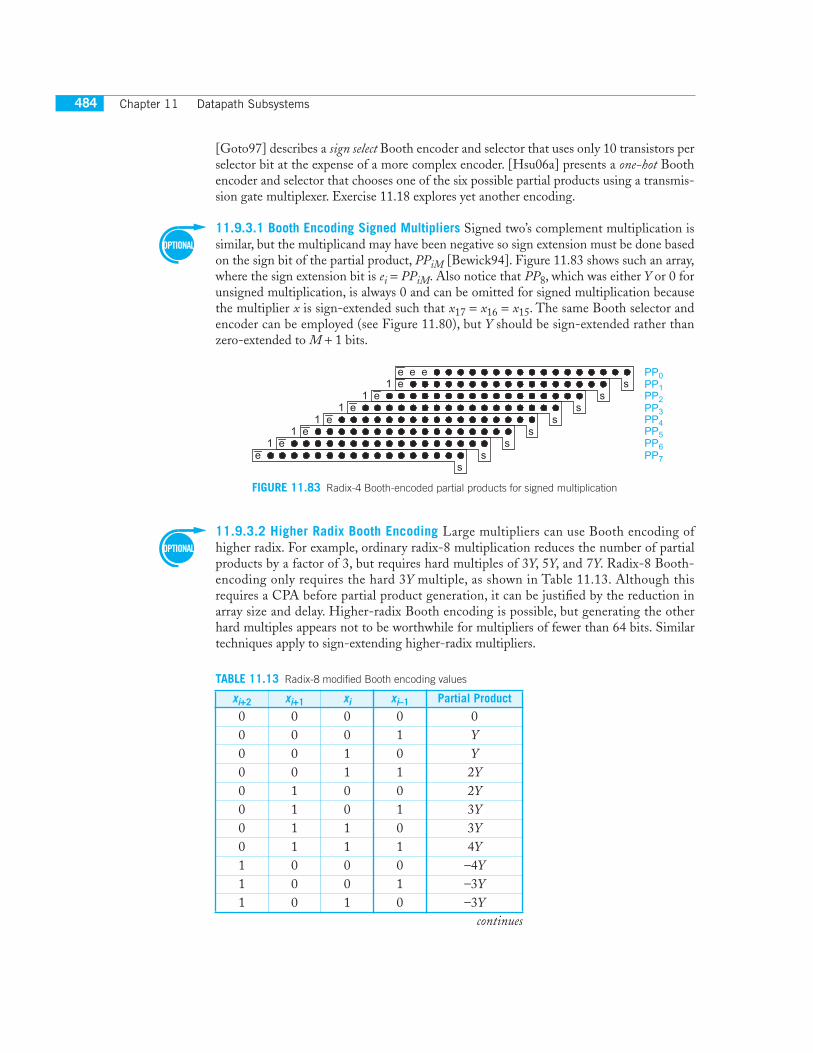
Chapter 11 Datapath Subsystems484
[Goto97] describes a sign select Booth encoder and selector that uses only 10 transistors perselector bit at the expense of a more complex encoder. [Hsu06a] presents a one-hot Boothencoder and selector that chooses one of the six possible partial products using a transmis-sion gate multiplexer. Exercise 11.18 explores yet another encoding.
11.9.3.1 Booth Encoding Signed Multipliers Signed two’s complement multiplication issimilar, but the multiplicand may have been negative so sign extension must be done basedon the sign bit of the partial product, PPiM [Bewick94]. Figure 11.83 shows such an array,where the sign extension bit is ei = PPiM. Also notice that PP8, which was either Y or 0 forunsigned multiplication, is always 0 and can be omitted for signed multiplication becausethe multiplier x is sign-extended such that x17 = x16 = x15. The same Booth selector andencoder can be employed (see Figure 11.80), but Y should be sign-extended rather thanzero-extended to M + 1 bits.
11.9.3.2 Higher Radix Booth Encoding Large multipliers can use Booth encoding ofhigher radix. For example, ordinary radix-8 multiplication reduces the number of partialproducts by a factor of 3, but requires hard multiples of 3Y, 5Y, and 7Y. Radix-8 Booth-encoding only requires the hard 3Y multiple, as shown in Table 11.13. Although thisrequires a CPA before partial product generation, it can be justified by the reduction inarray size and delay. Higher-radix Booth encoding is possible, but generating the otherhard multiples appears not to be worthwhile for multipliers of fewer than 64 bits. Similartechniques apply to sign-extending higher-radix multipliers.
TABLE 11.13 Radix-8 modified Booth encoding values
xi+2 xi+1 xi xi–1 Partial Product
0 0 0 0 00 0 0 1 Y0 0 1 0 Y0 0 1 1 2Y0 1 0 0 2Y0 1 0 1 3Y0 1 1 0 3Y0 1 1 1 4Y1 0 0 0 –4Y1 0 0 1 –3Y1 0 1 0 –3Y
seee
se1
se1
se1
se1
se1
se1
se
PP0PP1PP2PP3PP4PP5PP6PP7
FIGURE 11.83 Radix-4 Booth-encoded partial products for signed multiplication
continues

11.9 Multiplication 485
11.9.4 Column AdditionThe critical path in a multiplier involves summing the dots in each column. Observe thata CSA is effectively a “ones counter” that adds the number of 1s on the A, B, and C inputsand encodes them on the sum and carry outputs, as summarized in Table 11.14. A CSA istherefore also known as a (3,2) counter because it converts three inputs into a countencoded in two outputs [Dadda65]. The carry-out is passed to the next more significantcolumn, while a corresponding carry-in is received from the previous column. This iscalled a horizontal path because it crosses columns. For simplicity, a carry is represented asbeing passed directly down the column. Figure 11.84 shows a dot diagram of an arraymultiplier column that sums N partial products sequentially using N–2 CSAs. For exam-ple, the 16 × 16 Booth-encoded multiplier from Figure 11.82(b) sums nine partial prod-ucts with seven levels of CSAs. The output is produced in carry-save redundant formsuitable for the final CPA.
The column addition is slow because only one CSA is active at atime. Another way to speed the column addition is to sum partial prod-ucts in parallel rather than sequentially. Figure 11.85 shows a Wallace treeusing this approach [Wallace64]. The Wallace tree requires
levels of (3,2) counters to reduce N inputs down to two carry-save redun-dant form outputs.
Even though the CSAs in the Wallace tree are shown in two dimen-sions, they are logically packed into a single column of the multiplier.This leads to long and irregular wires along the column to connect theCSAs. The wire capacitance increases the delay and energy of multiplier,and the wires can be difficult to lay out.
1 0 1 1 –2Y1 1 0 0 –2Y1 1 0 1 –Y1 1 1 0 –Y1 1 1 1 –0
TABLE 11.14 An adder as a ones counter
A B C Carry Sum Number of 1s
0 0 0 0 0 00 0 1 0 1 10 1 0 0 1 10 1 1 1 0 21 0 0 0 1 11 0 1 1 0 21 1 0 1 0 21 1 1 1 1 3
TABLE 11.13 Radix-8 modified Booth encoding values
log /3 2 2N( )⎡⎢ ⎤⎥
abc
SumCarry
(3,2) CSA
Par
tial P
rodu
cts
RedundantOutput
FIGURE 11.84 Dot diagram for array multiplier
Par
tial P
rodu
cts
RedundantOutput
FIGURE 11.85 Dot diagram for Wallace tree multiplier
(continued)

Chapter 11 Datapath Subsystems486
11.9.4.1 [4:2] Compressor Trees [4:2] compressors can be used in a binary tree to producea more regular layout, as shown in Figure 11.86 [Weinberger81, Santoro89]. A [4:2] com-pressor takes four inputs of equal weight and produces two outputs. It can be constructedfrom two (3,2) counters as shown in Figure 11.87. Along the way, it generates an interme-
diate carry, ti, into the next column and accepts a carry, ti–1, from the previous col-umn, so it may more aptly be called a (5,3) counter. This horizontal path does notimpact the delay because the output of the top CSA in one column is the input ofthe bottom CSA in the next column. The [4:2] CSA symbol emphasizes only theprimary inputs and outputs to emphasize the main function of reducing fourinputs to two outputs. Only
levels of [4:2] compressors are required, although each has greater delay than aCSA. The regular layout and routing also make the binary tree attractive.
To see the benefits of a [4:2] compressor, we introduce the notion of fast andslow inputs and outputs. Figure 11.88 shows a simple gate-level CSA design. Thelongest path through the CSA involves two levels of XOR2 to compute the sum.X is called a fast input, while Y and Z are slow inputs because they pass through asecond level of XOR. C is the fast output because it involves a single gate delay,while S is the slow output because it involves two gate delays. A [4:2] compressormight be expected to use four levels of XOR2s. Figure 11.89 shows various [4:2]compressor designs that reduce the critical path to only 3 XOR2s. In Figure11.89(a), the slow output of the first CSA is connected to the fast input of the sec-ond. In Figure 11.89(b), the [4:2] compressor has been munged into a single cell,
log2 2N( )⎡⎢ ⎤⎥
WX Y Z
SC
MAJ
0 1
WX Y Z
MAJ
MAJ
ti − 1
ti − 1
ti
ti
ti − 1ti
SC
WX Y Z
SC
[3:2]CSA
[3:2]CSA
XN
OR
XN
OR
(a) (b) (c)
FIGURE 11.89 [4:2] compressors
Par
tial P
rodu
cts
RedundantOutput
FIGURE 11.86 Dot diagram for [4:2] tree multiplier
W X Y Z
SC
ti − 1ti
(a) (b)
W X Y Z
SC
FIGURE 11.87 [4:2] compressor (a) implementation with two CSAs (b) symbol
X Y Z
MAJ
SC
FIGURE 11.88 Gate-level carry-save adder

11.9 Multiplication 487
allowing a majority gate to be replaced with a multiplexer. InFigure 11.89(c), the initial XORs have been replaced with 2-levelXNOR circuits that allow some sharing of subfunctions, reduc-ing the transistor count [Goto92].
Figure 11.90 shows a transmission gate implementation of a[4:2] compressor from [Goto97]. It uses only 48 transistors,allowing for a smaller multiplier array with shorter wires. Notethat it uses three distinct XNOR circuit forms and two transmis-sion gate multiplexers.
Figure 11.91 compares floorplans of the 16 × 16 Booth-encoded array multiplier from Figure 11.84, the Wallace treefrom Figure 11.85, and the [4:2] tree from Figure 11.86. Eachrow represents a horizontal slice of the multiplier containing aBooth selector or a CSA. Vertical busses connect CSAs. TheWallace tree has the most irregular and lengthy wiring. In prac-tice, the parallelogram may be squashed into a rectangular formto make better use of the space. [Itoh01n] and [Huang05]describes floorplanning issues in tree multipliers.
11.9.4.2 Three-Dimensional Method The notion of connectingslow outputs to fast inputs generalizes to compressors with morethan four inputs. By examining the entire partial product array atonce, one can construct trees for each column that sum all of thepartial products in the shortest possible time. This approach is called the three-dimensionalmethod (TDM) because it considers the arrival time as a third dimension along with rowsand columns [Oklobdzija96, Stelling98].
Figure 11.92 shows an example of a 16 × 16 multiplier. The parallelogram at the topshows the dot diagram from Figure 11.82(b) containing nine partial product rowsobtained through Booth encoding. The partial products in each of the 32 columns must besummed to produce the 32-bit result. As we have seen, this is done with a compressor toproduce a pair of outputs, followed by a final CPA.
ti ti − 1
S C
WX Y Z
XNOR
XNOR
XNORX
NO
R
MUX
MUX
FIGURE 11.90 Transmission gate [4:2] compressor
Redundant Output
PP0
0Booth Selector(s)Booth Selector + CSA
PP8
Level 1CSA
Redundant Output Redundant Output
31 15
031 15PP2:0
PP5:3
PP8:6
PP3:0
PP7:4
PP8
[4:2] CSA
[4:2] CSA[4:2] CSA
[4:2] CSA
031 15
Level 2CSALevel 3CSALevel 4CSA
(a)
(b) (c)
FIGURE 11.91 16 × 16 Booth-encoded multiplier floorplans: (a) array, (b) Wallace tree, (c) [4:2] tree

Chapter 11 Datapath Subsystems488
In the three-dimensional method, each column is summed with a verticalcompressor slice (VCS) made of CSAs. In Figure 11.92, VCS 16 adds nine par-tial products. In this diagram, the horizontal carries between compressor slicesare shown explicitly.
Each wire is labeled with its arrival time. All partial product inputs arriveat time 0. The diagram assumes that an XOR2 and a majority gate each haveunit delay. Thus, a path through a CSA from any input to C or from X to Stakes one unit delay, and that a path from Y or Z to S takes two unit delays. Ahalf adder is assumed to have half the delay. Horizontal carries are representedby diagonal lines coming from behind the slice or pointing out of the slice.VCS 16 receives five horizontal carries in from VCS 15 and produces six hori-zontal carries out to VCS 17. The final carry out is also shifted by one columnbefore driving the CPA. The inputs to the CSAs are arranged based on theirarrival times to minimize the delay of the multiplier. Note how the CSA shapeis drawn to emphasize the asymmetric delays. Also, note that VCS 16 is notthe slowest; some of the subsequent slices have one unit more delay becausethe horizontal carries arrive later. [Oklobdzija96] describes an algorithm forchoosing the fastest arrangement of CSAs in each VCS given arbitrary CSAdelays. In comparison, Figure 11.93 shows the same VCS 16 using [4:2]CSAs; more XOR levels are required but the wiring is more regular.
ssss
ss1
ss1
ss1
ss1
ss1
ss1
ss
0 0 0 0 0 0 0 0
0.5
1
.52 2
2 2.5
2.5
3.5
1 1
221
1
2
3
4
55
43
3
5
3
To CPA
Final CPA
VCS 0
VCS 4
VCS 16VCS
32
VCS 26
CSA CSA
CSA
CSACSA
CSA
HA
CSA
X Y Z
CS
Legend
X, Y, Z arrive at same timeC ready faster than S
CSA
X Y Z
C S
X arrives slightly later than Y and ZC ready slightly faster than S
XY Z
C S
CSAX arrives much later than Y and ZC ready at same time as S
Tim
e
FIGURE 11.92 Vertical compressor slices in a TDM multiplier
4:2 4:2
4:2
11
0 0 0 0
33
1
10 0 0 0
33
33
334
46 6
6 0 6
88
FIGURE 11.93 Vertical compressor slice using [4:2] compressors

11.9 Multiplication 489
Table 11.15 lists the number of XOR levels on the critical path for various numbers ofpartial products. [4:2] trees offer a substantial improvement over Wallace trees in logic lev-els as well as wiring complexity. TDM generally saves one level of XOR over [4:2] trees, ormore for very large multiplies. This savings comes at the cost of irregular wiring, so [4:2]trees and variants thereof remain popular.
11.9.4.3 Hybrid Multiplication Arrays offer regular layout, but many levels of CSAs.Trees offer fewer levels of CSAs, but less regular layout and some long wires. A number ofhybrids have been proposed that offer trade-offs between these two extremes. Theseinclude odd/even arrays [Hennessy90], arrays of arrays [Dhanesha95], balanced delay trees[Zuras86], overturned-staircase trees [Mou90], and upper/lower left-to-right leapfrog(ULLRF) trees [Huang05]. They can achieve nearly as few levels of logic as the Wallacetree while offering more regular (and faster) wiring. None have caught on as distinctly bet-ter than [4:2] trees.
11.9.5 Final AdditionThe output of the partial product array or tree is an M + N-bit number in carry-saveredundant form. A CPA performs the final addition to convert the result back to nonre-dundant form.
The inputs to the CPA have nonuniform arrival times. As Figure 11.91 illustrated,the partial products form a parallelogram, with the middle columns having more partialproducts than the left or right columns. Hence, the middle columns arrive at the CPAlater than the others. This can be exploited to simplify the CPA [Zimmermann96,Oklobdzija96]. Figure 11.94 shows an example of a 32-bit prefix network that takesadvantage of nonuniform arrival times out of a 16 × 16-bit multiplier. The initial and finalstages to compute bitwise PG signals and the sums are not shown. The path from the lat-est middle inputs to the output involves only four levels of cells. The total number of cells
TABLE 11.15 Comparison of XOR levels in multiplier trees
# Partial Products Wallace Tree 4:2 Tree TDM
8 8 6 59 8 8 616 12 9 824 14 11 1032 16 12 1164 20 15 14
012345678910111213141516171819202122232425262728293031
Time
FIGURE 11.94 CPA prefix network with nonuniform input arrival times

Chapter 11 Datapath Subsystems490
and the energy consumption is much less than that of a conventional Kogge-Stone orSklansky CPA.
11.9.6 Fused Multiply-AddMany algorithms, particularly in digital signal processing, require computing P = X × Y +Z. While this can be done with a multiplier and adder, it is much faster to use a fusedmultiply-add unit, which is simply an ordinary multiplier modified to accept another inputZ that is summed just like the other partial products [Montoye90]. The extra partial prod-uct increases the delay of an array multiplier by just one extra CSA.
11.9.7 Serial MultiplicationThis section is available in the online Web Enhanced chapter at www.cmosvlsi.com.
11.9.8 SummaryThe three steps of multiplication are partial product generation, partial product reduction,and carry propagate addition. A simple M × N multiplier generates N partial productsusing AND gates. For multipliers of 16 or more bits, radix-4 Booth encoding is typicallyused to cut the number of partial products in two, saving substantial area and power. Someimplementations find Booth encoding is faster, while others find it has little speed benefit.The partial products are then reduced to a pair of numbers in carry-save redundant formusing an array or tree of CSAs. Trees have fewer levels of logic, but longer and less regularwiring; nevertheless most large multipliers use trees or hybrid structures. Pass transistorBooth selectors and CSAs were popular in the 1990s, but the trend is toward staticCMOS as supply voltage scales. Finally, a CPA converts the result to nonredundant form.The CPA can be simplified based on the nonuniform arrival times of the bits.
Table 11.16 compares reported implementations of 54 × 54-bit multipliers for double-precision floating point arithmetic. All of the implementations use radix-4 Booth encoding.
TABLE 11.16 54 × 54-bit multipliers
Design Process (mm)
PP Reduction
Circuits Area (mm × mm)
Area (Ml2)
Transistors Latency (ns)
Power (mW)
[Mori91] 0.5 4:2 tree Pass Transistor
XOR
3.6 × 3.5 200 82k 10 870
[Goto92] 0.8 4:2 tree Static 3.4 × 3.9 80 83k 13 875 [Heikes94] 0.8 array Dual-Rail
Domino2.1 × 2.2 28 20
(2-stage pipeline)[Ohkubo95] 0.25 4:2 tree Pass
Transistors3.7 × 3.4 805 100k 4.4
[Goto97] 0.25 4:2 tree Pass Transistors
1.0 × 1.3 84 61k 4.1
[Itoh01] 0.18 4:2 tree Static 1 × 1 100 3.2(2-stage pipeline)
[Belluomini05] 90 nm 3:2 and 4:2 tree
LSDL 0.4 × 0.3 61 1800 @ 8 GHz
[Kuang05] 90 nm 3:2 and 4:2 tree
Pass Transistor
and Domino
0.5 × 0.4 94 426 @ 4 GHz
WEBENHANCED

11.10 Parallel-Prefix Computations 491
11.10 Parallel-Prefix Computations Many datapath operations involve calculating a set of outputs from a set of inputs in whicheach output bit depends on all the previous input bits. Addition of two N-bit inputs AN…A1and BN…B1 to produce a sum output YN…Y1 is a classic example; each output Yi depends ona carry-in ci–1 from the previous bit, which in turn depends on a carry-in ci–2 from the bitbefore that, and so forth. At first, this dependency chain might seem to suggest that thedelay must involve about N stages of logic, as in a carry-ripple adder. However, we have seenthat by looking ahead across progressively larger blocks, we can construct adders that involveonly log N stages. Section 11.2.2.2 introduced the notion of addition as a prefix computationthat involves a bitwise precomputation, a tree of group logic to form the prefixes, and a finaloutput stage, shown in Figure 11.12. In this section, we will extend the same techniques toother prefix computations with associative group logic functions.
Let us begin with the priority encoder shown in Figure 11.95. A common applicationof a priority encoder circuit is to arbitrate among N units that are all requesting access to ashared resource. Each unit i sends a bit Ai indicating a request and receives a bit Yi indicat-ing that it was granted access; access should only be granted to a single unit with highestpriority. If the least significant bit of the input corresponds to the highest priority, thelogic can be expressed as follows:
(11.33)
We can express priority encoding as a prefix operation by defining a prefix Xi:j indi-cating that none of the inputs Ai…Aj are asserted. Then, priority encoding can be definedwith bitwise precomputation, group logic, and output logic with i ≥ k > j:
(11.34)
Any of the group networks (e.g., ripple, skip, lookahead, select, increment, tree) dis-cussed in the addition section can be used to build the group logic to calculate the Xi:0 pre-fixes. Short priority encoders use the ripple structure. Medium-length encoders may use askip, lookahead, select, or increment structure. Long encoders use prefix trees to obtain logN delay. Figure 11.96 shows four 8-bit priority encoders illustrating the different grouplogic. Each design uses an initial row of inverters for the Xi:i precomputation and a finalrow of AND gates for the Yi output logic. In between, ripple, lookahead, increment, andSklansky networks form the prefixes with various trade-offs between gate count and delay.Compare these trees to Figure 11.15, Figure 11.22, Figure 11.25, and Figure 11.29(b),respectively. [Wang00, Delgado-Frias00, Huang02] describe a variety of priority encoderimplementations.
An incrementer can be constructed in a similar way. Adding 1 to an input word con-sists of finding the least significant 0 in the word and inverting all the bits up to this point.The X prefix plays the role of the propagate signal in an adder. Again, any of the prefixnetworks can be used with varying area-speed trade-offs.
Y A
Y A A
Y A A A
Y A AN N N
1 1
2 2 1
3 3 2 1
1
=
= ⋅
= ⋅ ⋅
= ⋅ ⋅−
...
.... ⋅ A1
X A
X X Xi i i
i j i k k j
:
: : :
== ⋅ −
bitwise precomputation
gr1 ooup logic
output logicY A Xi i i= ⋅ −1 1:
A1A2
AN
Y1Y2
YN
Prio
rity
Enc
oder
FIGURE 11.95 Priority encoder

Chapter 11 Datapath Subsystems492
(11.35)
Decrementers and two’s complement circuits are also similar [Hashemian92]. The decre-menter finds the least significant 1 and inverts all the bits up to this point. The two’s comple-ment circuit negates a signed number by inverting all the bits above the least significant 1.
A binary-to-thermometer decoder is another application of a prefix computation. Theinput B is a k-bit representation of the number M. The output Y is a 2k-bit number withthe M most significant bits set to 1, as given in Table 11.17. A simple approach is to use anordinary k:2k decoder to produce a one-hot 2k-bit word A. Then, the following prefixcomputation can be applied:
X A
X X Xi i i
i j i k k j
:
: : :
== ⋅ −
bitwise precomputation
gr1 ooup logic
output logicY A Xi i i= ⊕ −1 1:
X2:1
X3:1
X4:1
X5:1
X6:5
X7:5
A8 A1A2A3A4A5A6A7
A8 A1A2A3A4A5A6A7
Y8 Y1Y2Y3Y4Y5Y6Y7
Y8 Y1Y2Y3Y4Y5Y6Y7
Y8 Y1Y2Y3Y4Y5Y6Y7
Y8 Y1Y2Y3Y4Y5Y6Y7
X1X2X3X4X5X6X7
A8 A1A2A3A4A5A6A7
A8 A1A2A3A4A5A6A7
X1X2X3X4X5X6X7
A8 A1A2A3A4A5A6A7
A8 A1A2A3A4A5A6A7
X1X2X3X4X5X6X7
A8 A1A2A3A4A5A6A7
A8 A1A2A3A4A5A6A7
X1X2X3X4X5X6X7
X2:1
X3:1
X4:1
X5:1
X6:1
X7:1
X6:1X7:1
X2:1
X4:3
X4:1
X
X6:5X7:5
X6:1X7:1
X2:1
X3:1
X4:1
X5:1
X6:1
X4:1
X7:1
(a) Ripple (b) Lookahead
(c) Increment (d) Sklansky
5:1
FIGURE 11.96 Priority encoder trees

11.11 Pitfalls and Fallacies 493
(11.36)
TABLE 11.17 Binary to thermometer decoder
B Y000 00000000001 10000000010 11000000011 11100000100 11110000101 11111000110 11111100111 11111110
X A
X X Xi i N i
i j i k k j
:
: : :
== +
−
−
bitwise precomputation
1 ggroup logic
output logicY Xi i= :0
3:8 DecoderB2:0
111110101100011010001000
0
B2B1B0
0
X1X2X4X6 X3X5X7
Y1 Y0Y2Y3Y4Y5Y6Y7
Y1 Y0Y2Y3Y4Y5Y6Y7
(a)
(b)
FIGURE 11.97 Binary-to-thermometer decoders
Figure 11.97(a) shows an 8-bit binary-to-thermometer decoder using aSklansky tree. The 3:8 decoder contains eight 3-input AND gates operating ontrue and complementary versions of the input. However, the logic can be signifi-cantly simplified by eliminating the complemented AND inputs, as shown inFigure 11.97(b)
In a slightly more complicated example, consider a modified priorityencoder that finds the first two 1s in a string of binary numbers. This might beuseful in a cache with two write ports that needs to find the first two free wordsin the cache. We will use two prefixes: X and W. Again, Xi:j indicates that noneof the inputs Ai…Aj are asserted. Wi:j indicates exactly one of the inputs Ai…Ajis asserted. We will produce two 1-hot outputs, Y and Z, indicating the firsttwo 1s.
(11.37)
11.11 Pitfalls and FallaciesEquating logic levels and delayComparing a novel design with the best existing design is difficult. Some engineers cut corners
by merely comparing logic levels. Unfortunately, delay depends strongly on the logical effort
of each stage, the fanout it must drive, and the wiring capacitance. For example, [Srinivas92]
claims that a novel adder is 20–28% faster than the fastest known binary lookahead adder, but
X AW A
X X X
i i i
i i i
i j i k
:
:
: :
==
= ⋅
bitwise precomputation
kk j
i j i k k j i k k j
i
W W X X W
Y
−
− −= ⋅ + ⋅1
1 1
:
: : : : : group logic
== ⋅= ⋅
−
−
A XZ A W
i i
i i i
1 1
1 1
:
: output logic
Chapter 11 Datapath Subsystems494
does not present simulation results. Moreover, it reports some of the speed advantages to three
or four significant figures. On closer examination [Dobson95], the adder proves to just be a hy-
brid tree/carry-select design with some unnecessary precomputation.
Designing circuits with threshold dropsIn modern processes, single-pass transistors that pull an output to VDD – Vt are generally un-
acceptable because the threshold drop (amplified by the body effect) results in an output with
too little noise margin. Moreover, when they drive the gate terminals of a subsequent stage,
the stage turns partially ON and consumes static power. Many 10-transistor full-adder cells
have been proposed that suffer from such a threshold drop problem.
Reinventing addersThere is an enormous body of literature on adders with various trade-offs among speed, area,
and power consumption. The design space has been explored fairly well and many designers
(one of the authors included) have spent quite a bit of time developing a “new” adder, only to
find that it is only a minor variation on an existing theme. Similarly, a number of recent pub-
lications on priority encoders reinvent prefix network techniques that have already been ex-
plored in the context of addition.
SummaryThis chapter has presented a range of datapath subsystems. How one goes about designingand implementing a given CMOS chip is largely affected by the availability of tools, theschedule, the complexity of the system, and the final cost goals of the chip. In general, thesimplest and least expensive (in terms of time and money) approach that meets the targetgoals should be chosen. For many systems, this means that synthesis and place & route isgood enough. Modern synthesis tools draw on a good library of adders and multiplierswith various area/speed trade-offs that are sufficient to cover a wide range of applications.For systems with the most stringent requirements on performance or density, customdesign at the schematic level still provides an advantage. Domino parallel-prefix trees pro-vide the fastest adders when the high power consumption can be tolerated. Domino CSAsare also used in fast multipliers. However, in multiplier design, the wiring capacitance isparamount and a multiplier with compact cells and short wires can be fast as well as smalland low in power.
Exercises11.1 Design a fast 8-bit adder. The inputs may drive no more than 30 λ of transistor
width each and the output must drive a 20/10 λ inverter. Simulate the adder and determine its delay.
11.2 When adding two unsigned numbers, a carry-out of the final stage indicates an overflow. When adding two signed numbers in two’s complement format, overflow detection is slightly more complex. Develop a Boolean equation for overflow as a function of the most significant bits of the two inputs and the output.

Exercises 495
11.3 Repeat Exercise 11.2 for a signed add/subtract unit like that shown in Figure 11.41(b). Your overflow output should be a function of the subsignal and the most significant bits of the two inputs and the output.
11.4 Develop equations for the logical effort and parasitic delay with respect to the C0 input of an n-stage Manchester carry chain computing C1…Cn. Consider all of the internal diffusion capacitances when deriving the parasitic delay. Use the transistor widths shown in Figure 11.98 and assume the Pi and Gi transistors of each stage share a single diffusion contact.
P1φ
G1
φ
G2
P2φ
Gn
Pn
C0 (G0)
C1 (G1:0)
Cn (Gn:0)
Cn − 1 (Gn − 1:0)
4 44
44
44
111
2/0.5 2/0.52/0.5
FIGURE 11.98 Manchester carry chain
11.5 Using the results of Exercise 11.4, what Manchester carry chain length gives the least delay for a long adder?
11.6 The carry increment adder in Figure 11.26(b) with variable block size requires five stages of valency-2 group PG cells for 16-bit addition. How many stages are required for 32-bit addition? For 64-bit addition?
11.7 Sketch the PG network for a modified 16-bit Sklansky adder with fanout of [8, 1, 1, 1] rather than [8, 4, 2, 1]. Use buffers to prevent the less-significant bits from loading the critical path.
11.8 Figure 11.29 shows PG networks for various 16-bit adders and Figure 11.30 illus-trates how these networks can be classified as the intersection of the l + f + t = 3 plane with the face of a cube. The plane also intersects one point inside the cube at (l, f, t) = (1, 1, 1) [Harris03]. Sketch the PG network for this 16-bit adder.
11.9 Sketch a diagram of the group PG tree for a 32-bit Ladner-Fischer adder.
11.10 Write a Boolean expression for Cout in the circuit shown in Figure 11.6(b). Simplify the equation to prove that the pass-transistor circuits do indeed compute the major-ity function.
11.11 Prove EQ (11.21).
11.12 Sketch a design for a comparator computing A – B = k.
11.13 Show how the layout of the parity generator of Figure 11.57 can be designed as a linear column of XOR gates with a tree-routing channel.
11.14 Design an ECC decoder for distance-3 Hamming codes with c = 3. Your circuit should accept a 7-bit received word and produce a 4-bit corrected data word. Sketch a gate-level implementation.
11.15 How many check bits are required for a distance-3 Hamming code for 8-bit data words? Sketch a parity-check matrix and write the equations to compute each of the check bits.

Chapter 11 Datapath Subsystems496
11.16 Find the 4-bit binary-reflected Gray code values for the numbers 0–15.
11.17 Design a Gray-coded counter in which only one bit changes on each cycle.
11.18 Table 11.12 and Figure 11.80 illustrated radix-4 Booth encoding using SINGLE, DOUBLE, and NEG. An alternative encoding is to use POS, NEG, and DOUBLE. POS is true for the multiples Y and 2Y. NEG is true for the multiples –Y and –2Y. DOUBLE is true for the multiples 2Y and –2Y. Design a Booth encoder and selector using this encoding.
11.19 Adapt the priority encoder logic of EQ (11.37) to produce three 1-hot outputs corresponding to the first three 1s in an input string.
11.20 Sketch a 16-bit priority encoder using a Kogge-Stone prefix network.
11.21 Use Logical Effort to estimate the delay of the priority encoder from Exercise 11.20. Assume the path electrical effort is 1.
11.22 Write equations for a prefix computation that determines the second location in which the pattern 10 appears in an N-bit input string. For example, 010010 should return 010000.
11.23 [ Jackson04] proposes an extension of the Ling adder formulation to simplify cells later in the prefix network. Design a 16-bit adder using this technique and com-pare it to a conventional 16-bit Ling adder.