
JUKKA VIINAMAKI¨ DESIGN AND IMPLEMENTATION OF A BOOST ...
63
TAMPERE UNIVERSITY OF TECHNOLOGY Department of Electrical Engineering JUKKA VIINAM ¨ AKI DESIGN AND IMPLEMENTATION OF A BOOST-POWER-STAGE CONVERTER FOR PHOTOVOLTAIC APPLICATION Master of Science Thesis Examiner: Teuvo Suntio The examiner and the topic were ap- proved in the Faculty of Computing and Electrical Engineering Council meeting on 3.10.2012 brought to you by CORE View metadata, citation and similar papers at core.ac.uk provided by Trepo - Institutional Repository of Tampere University
Transcript of JUKKA VIINAMAKI¨ DESIGN AND IMPLEMENTATION OF A BOOST ...

TAMPERE UNIVERSITY OF TECHNOLOGY
Department of Electrical Engineering
JUKKA VIINAMAKIDESIGN AND IMPLEMENTATION OF ABOOST-POWER-STAGE CONVERTER FORPHOTOVOLTAIC APPLICATIONMaster of Science Thesis
Examiner: Teuvo Suntio
The examiner and the topic were ap-
proved in the Faculty of Computing and
Electrical Engineering Council meeting
on 3.10.2012
brought to you by COREView metadata, citation and similar papers at core.ac.uk
provided by Trepo - Institutional Repository of Tampere University

ii
TIIVISTELMA
TAMPEREEN TEKNILLINEN YLIOPISTO
Sahkotekniikan diplomi-insinoorin tutkinto
JUKKA VIINAMAKI: Design and Implementation of a
Boost-Power-Stage Converter for
Photovoltaic Application
Diplomityo, 51 sivua, 4 liitesivua
Kesakuu 2013
Paaaine: Sahkokayttojen tehoelektroniikka
Tarkastaja: Prof. Teuvo Suntio
Avainsanat: aurinkosahkojarjestelma, mitoitus,
suunnittelu, saatosuunnittelu
Aurinkopaneeli muuttaa auringosta tulevan sahkomagneettisen sateilyn sahkoenergiak-
si, joka voidaan siirtaa sahkoverkkoon tehoelektroniikan avulla. Aurinkopaneelin suu-
rin lahtoteho, oikosulkuvirran arvo ja avoimen piirin jannite riippuvat ymparoivasta
lampotilasta ja sateilytehotiheyden arvosta. Niiden suurimmat mahdolliset arvot on
tarkeaa tietaa suunniteltaessa aurinkopaneeliin kytkettya hakkuriteholahdetta. Oiko-
sulkuvirran ja avoimen piirin jannitteen suurimmat mahdolliset arvot saatiin selville
ymparivuotisen sateilytehotiheyden ja lampotilan mittaustiedon perusteella.
Tassa tyossa suunniteltiin kaksi boost-tyyppista hakkuriteholahdetta, joista ensimmai-
sen mitoitus perustui kirjallisuudessa esitettyyn menetelmaan. Siina kelan ja puolijoh-
teiden mitoituksessa kaytettavan virran arvo laskettiin jakamalla teholahteeseen syo-
tetty teho sisaanmenojannitteen minimiarvolla. Toisen teholahteen mitoituksessa kelan
ja puolijohteiden mitoituksessa kaytettavan virran arvona kaytettiin suoraan tietoa au-
rinkopaneelin suurimmasta mahdollisesta oikosulkuvirran arvosta.
Teholahteet suunniteltiin siten, etta molemmissa on yhta suuri kytkentataajuinen tu-
lojannitteen aaltoisuus ja kyky vaimentaa lahtojannitteessa nakyvaa matalataajuista
aaltoisuutta siten, etta se ei nakyisi tulojannitteessa. Vaikka teholahteet toimivat tal-
ta osin sahkoisesti samalla tavalla, ensimmainen mitoitustapa johti suurempaan tulon
kapasitanssiin ja suurempaan kelan sydamen kokoon seka epatasaisempaan puolijoh-
dekomponenttien lampotilajakaumaan maksimitehpisteessa kuin jalkimmainen mitoi-
tustapa. Kirjallisuudessa esitetylla mitoitustavalla paadytaan siis ylimitoitukseen. Jos
mitoitus tehdaan tassa tyossa esitellylla uudella tavalla, voidaan saada aikaan huomat-
tavia kustannussaastoja varsinkin suuremmissa jarjestelmissa, joissa tehot ovat suuria.
Suunnitelluista teholahteista rakennettiin prototyypit, joita mittaamalla edella esitetyt
tulokset varmennettiin.
iii
ABSTRACT
TAMPERE UNIVERSITY OF TECHNOLOGY
Master’s Degree Programme in Electrical Engineering
JUKKA VIINAMAKI: Design and Implementation of a
Boost-Power-Stage Converter for
Photovoltaic Application
Master of Science Thesis, 51 pages, 4 Appendix pages
June 2013
Major: Power Electronics in Electrical Drives
Examiner: Prof. Teuvo Suntio
Keywords: photovoltaic, current-fed, boost converter, component sizing, PV, design
Photovoltaic generator is a device that converts solar radiation originated from the Sun
into electrical energy. Power electronics are used to feed this electrical energy into the
grid. In the design of a converter that is connected to the photovoltaic generator, it
is important to know the maximum values of the generator output: Maximum out-
put power, short-circuit current and open-circuit voltage, which are dependent on the
amount of incident radiation and the value of ambient temperature. Maximum value
for short-circuit current and open-circuit voltage were found based on the year-round
irradiation and temperature measurement data.
In this thesis, two boost-power-stage converters were designed. Design of the first con-
verter was based on the conventional method that was introduced in the literature. In
that method, the inductor and semiconductors were sized by using current that was
derived by dividing input power of the converter by input voltage. Value of the con-
verter input power was calculated by multiplying the standard test condition output
power of the selected photovoltaic generator by conventional sizing factor, which is the
ratio of the converter nominal input power to the nominal output power of the photo-
voltaic generator. The second converter was designed by using the information about
the real maximum output current of the selected photovoltaic generator, which is the
short-circuit current.
The converters were designed in such a way that both have the same amount of switch-
ing frequency input voltage ripple and equal ability to prevent the low frequency output
voltage ripple from affecting the input voltage. Even if the converters are electrically
similar, the conventional design method leads to higher input capacitance, larger induc-
tor core size and more uneven temperature distribution of the power semiconductors at
the maximum power point than the new design method. Thus, the conventional design
method leads to unnecessary oversizing. Significant cost savings can be achieved by
applying the new design method, which is presented in this thesis for the first time.
The results were verified by experimental measurements.

iv
PREFACE
This Master of Science thesis was done for the Department of Electrical Engineering at
Tampere University of Technology. The examiner of the thesis was Prof. Teuvo Suntio.
I want to express my gratitude to Prof. Teuvo Suntio for the interesting topic and
guidance through the project. I also want to thank M.Sc. Tuomas Messo and M.Sc.
Juha Jokipii for helping me with the converter model and with all kind of practical
issues. Finally I want to thank the rest of the working group, especially M.Sc. Anssi
Maki for the information about the measurement system and the discussions about the
properties of a photovoltaic generator.
Tampere 17.05.2013
Jukka Viinamaki

v
CONTENTS
1. Introduction . . . . . . . . . . . . . . . . . . . . . . . . . . . . . . . . . . . . 1
2. Properties of a Photovoltaic Module . . . . . . . . . . . . . . . . . . . . . . . 3
2.1 Modeling of a Photovoltaic Module . . . . . . . . . . . . . . . . . . . . . 3
2.2 Effect of Climate Conditions on the PV Module . . . . . . . . . . . . . . 6
2.3 Limit Values of NAPS NP190GKg PV Module Output . . . . . . . . . . 8
3. Operation of a Boost-Power-Stage Converter . . . . . . . . . . . . . . . . . . 12
3.1 Dynamic Modeling . . . . . . . . . . . . . . . . . . . . . . . . . . . . . . 13
3.2 The Effect of Nonideal Source . . . . . . . . . . . . . . . . . . . . . . . . 18
4. Converter Design . . . . . . . . . . . . . . . . . . . . . . . . . . . . . . . . . . 20
4.1 Maximum Input Current and Voltage . . . . . . . . . . . . . . . . . . . 20
4.2 Inductor Design . . . . . . . . . . . . . . . . . . . . . . . . . . . . . . . 21
4.3 Selection of MOSFET and Diode . . . . . . . . . . . . . . . . . . . . . . 26
4.4 Thermal Design . . . . . . . . . . . . . . . . . . . . . . . . . . . . . . . 33
4.5 Control Design and Selection of Input Capacitor . . . . . . . . . . . . . 34
5. Measurements . . . . . . . . . . . . . . . . . . . . . . . . . . . . . . . . . . . 39
5.1 Prototypes . . . . . . . . . . . . . . . . . . . . . . . . . . . . . . . . . . 39
5.2 Thermal Distribution . . . . . . . . . . . . . . . . . . . . . . . . . . . . 40
5.3 Input Voltage Ripple . . . . . . . . . . . . . . . . . . . . . . . . . . . . . 44
5.4 Frequency Response Measurements . . . . . . . . . . . . . . . . . . . . . 44
6. Conclusions . . . . . . . . . . . . . . . . . . . . . . . . . . . . . . . . . . . . . 48
References . . . . . . . . . . . . . . . . . . . . . . . . . . . . . . . . . . . . . . . 49
A.Impedance Measurement of The Inductors . . . . . . . . . . . . . . . . . . . . 52
B.Schematics of The Prototype Converters . . . . . . . . . . . . . . . . . . . . . 54

vi
TERMS AND SYMBOLS
NOTATION
A System matrixAe Cross-sectional area of the coreAw Cross-sectional area of the wirea Diode ideality factorB Input matrixBAC,PEAK Peak value of alternating fluxBmax Maximum flux densityC Output matrixC Capacitance∆ Characteristic polynomial∆iL,pp Inductor current peak-to-peak rippled Duty ratiod′ Complement of duty ratioD Input-output matrixD Steady-state value of duty ratiofs Switching frequencyG IrradianceGn Irradiance in standard test conditionGa Gain of pulse width modulatorGc Controller transfer functionGci−o Open-loop control-to-input transfer functionGS
ci−o Source-affected open-loop control-to-input transfer functionGco−o Open-loop control-to-output transfer functionGS
co−o Source-affected open-loop control-to-output transfer functionGri Reference-to-input transfer functionGro Reference-to-output transfer functionG Matrix containing transfer functions of a converterGio−o Open-loop input-to-output transfer functionGio−∞ Ideal forward current gainGio-c Closed-loop input-to-output transfer functionGS
io-o Source-affected input-to-output transfer functionH Magnetic field strengthId,rms Root mean square of the diode currentiin Converter input currentio Converter output currentisc,n Short-circuit current in standard test conditionIsw,rms Root mean square of switch currentIL Steady-state value of inductor currentiinS Input current of non-ideal sourceiph Photocurrenti0 Saturation currentIL,p Peak value of inductor currentIMPP,STC Current in standard test conditionJ Flux densityK Window utilization factor

vii
lw Length of wirem MassI Identity matrixk Bolzmann constantKI Temperature coefficient of short-circuit currentKV Temperature coefficient of open-circuit voltageL InductanceLin Input voltage loop gainlm Core magnetic path lengthµ0 Permeability of free spaceµe Core permeabilityN Number of turnsNs Number of series connected cells in a photovoltaic modulePCU,DC Copper loss caused by direct currentPCORE Inductor core lossPd,cond Conduction loss of the diodePd,rev Power loss of the diode caused by reverse leakage currentPd,tot Total power loss of the diodePMPP,STC Power in standard test conditionPsw,c Conduction losses of power switchPsw,sw Switching losses of power switchPsw,tot Total power loss of power switchPTOT Total power loss of inductorq Electron chargeRth Thermal resistances Laplace variableT TemperatureTs Switching periodToi−o Open-loop reverse voltage transfer ratioToi-c Closed-loop reverse voltage transfer ratioT Soi-o Source-affected reverse voltage transfer ratio
UMPP,STC Voltage in standard test conditionuoc,n Open-circuit voltage in standard test conditionWaAc Core area productx AC-perturbation around a steady-state operation pointYo-o Open-loop output admittanceYo-c Closed-loop output admittanceY So-o Source-affected output admittance
Zin-o Open-loop input impedanceZin-c Closed-loop input impedanceZS
in-o Source-affected input impedanceYo−∞ Ideal output admittanceYS Output admittance of a non-ideal sourceZin−oco Open circuit input impedanceZin−∞ Ideal input impedance

viii
Zin−o Open-loop input impedanceZin−c Closed-loop input impedance
ABBREVIATIONS
CC Constant currentCCM Continous conduction modeCM Conventional methodCF Current-fedCV Constant voltageCO2 Carbon-dioxideDC Direct currentESR Equivalent series resistanceGM Gain marginMPP Maximum power pointMPPT Maximum power point trackingNM New methodOC Open-circuitPM Phase marginPV PhotovoltaicPV G Photovoltaic generatorPWM Pulse width modulationRMS Root mean squareSC Short-circuitSF Sizing factor

1
1. INTRODUCTION
Modern society is dependent on energy. Energy consumption is increasing mainly
because of growing world population and improvement of our standard of living. In
2010, 87% of the total energy was produced from non-renewable fuels such as oil, coal
and natural gas. About 6% was generated by nuclear power and the remaining 7%
came from renewable resources such as hydro, biofuel, wind, solar and geothermal.
With the present consumption, resources of non-renewable energy will run out in the
near future. In addition, burning of fossil fuels generates pollutant gases such as CO2,
which is proved to be the main reason for the global warming problem. Long-term
effect of global warming is very serious, since it will accelerate the gradual melting of
the world’s glaciers, which will increase the sea level. This has serious effect, since
100 million people live within 3ft above the sea water level. Global warmig will also
cause damage to vegetation and agriculture because of droughts. Extreme weather
conditions will happen more often and gulf stream might change substantially causing
freezing weather in some parts of the world [1].
This trend could be affected by covering greater part of the energy production by
renewable alternatives. It has been stated that 100% of the world’s energy demand
could be covered by hydro, wind and solar technologies [1]. Solar energy is one of the
most promising alternatives, since it is abundantly available. Solar insolation could be
used for heating but also conversion directly into electrical energy is possible using solar
cells. A solar cell is a special kind of semiconductor diode, which causes DC current to
flow when it is exposed to the light. Since the voltage of a single photovoltaic (PV) cell
is low, a number of cells have to be connected together to form a PV module. Typical
PV module includes tens of series connected PV cells. PV modules could be connected
in series to form strings and parallel to form arrays and this kind of entity is generally
called photovoltaic generator (PVG). Due to above mentioned reasons and because of
decreased price of PV modules, the number of annual PV installations is increasing
by the rate of 70%. As an example, installed annual global PV power reached about
30GW in 2011 [2].
Electrical energy that is produced by PVG can be fed into the grid or stored to an
energy storage. This could be done by means of power electronics, which is important
part of a PV power plant. As the amount of PV installations increases, it becomes more
and more important to develop the power converters to be energy efficient, economical
and reliable. All this means that the properties of the PVG should be taken into
account when designing power converters for PV applications.
In a typical case of building the PV power plant, system integrator buys the PV
modules and the power electronics from different manufacturers. Selection of the PV

1. Introduction 2
generator is mainly based on the standard test condition (STC) power that the manu-
facturer provides in the datasheet. Power electronic devices are further selected based
on the STC power of the PVG. In this stage, it is also checked that the maximum input
current and maximum input voltage of the selected converter are high enough for the
PVG. This leads to a situation, where the manufacturer of the converter would like to
make it as universal as possible.
References [3] and [4] show explicitly that the component sizing of an interleaved-
boost-power-stage for the PV application is based on the maximum input current that is
calculated by dividing the input power of the converter by minimum input voltage. This
sizing method leads to higher current than is possible to feed from the corresponding
PV generator leading to oversizing. By inspecting the datasheets of the solar inverters,
such a method seems to be commonly used [5],[6],[7]. These inverters are single-stage
inverters where the level of the dc voltage is directly determined by the grid voltage.
Therefore, the required dc voltage is much higher than defined in [3] and [4] leading to
lower generator current.
The main goal of the thesis is to study how the PV generator affects the design of
a power electronics converter connected directly to it. Two boost-power-stage DC/DC
converters have been used as design example. One is designed based on the conventional
design method and the other taking into account the special characteristics of a PV
generator. The designs are done by using the same electrical characteristics in terms
of input and output terminal ripple and power.
The rest of of the thesis is organized as follows: Chapter 2 presents the properties
of a PVG and the limiting values for the terminal characteristics of the selected PV
module are evaluated. Chapter 3 introduces the properties of a boost-power-stage
converter in PV application and also the results of dynamic analysis are presented.
Chapter 4 contains the complete design process starting from the specification and
ending to the control design. Chapter 5 presents the measurements of the prototypes
by illustrative graphs and the final chapter aggregates the most important results of
the study.

3
2. PROPERTIES OF A PHOTOVOLTAIC MODULE
2.1 Modeling of a Photovoltaic Module
Electrical characteristics of an ideal PV cell can be represented by a parallel connection
of a current source and a diode. The current source describes a photovoltaic current
iph, which is directly proportional to the incident radiation and the diode represent the
properties of a p−n junction. Practical PV cells also contain losses, which are included
in the model as shunt resistance rsh and series resistance rs as presented in Fig. 2.1. In
Fig. 2.1, id is the diode current, ud is the diode voltage, ish is the current through the
shunt resistance, ipv is the output current of the cell and upv is the terminal voltage of
the PV cell [8].
phi pvu
pvisr
shr
shidi
du
Figure 2.1: Single-diode model of a photovoltaic cell.
In addition to a single PV cell, single-diode model in Fig. 2.1 could also represent
a PV module, which constitutes of several cells connected in series. Equation that
mathematically describes the I-U characteristics of the practical PV module is presented
in (2.1) [8].
ipv = iph − i0
[
exp
(
upv + rsipvNsakT/q
)
− 1
]
−upv + rsipv
rsh, (2.1)
where iph is the photocurrent generated by the incident light, i0 is the saturation
current, Ns is the number of series connected cells, a is the diode ideality factor, k is
the Bolzmann constant, T is the temperature of the p−n junction and q is the electron
charge. More sophisticated models have been developed but the single-diode model
offers good compromise between accuracy and complexity.
When the current ipv is zero, PV cell is said to operate in open-circuit condition
(OC). Respectively, when the voltage upv is zero, PV cell operate in short-circuit con-
dition (SC). In both of these conditions, the output power of the PV cell is zero and
the maximum output power is found to be in between of these conditions, which is

2. Properties of a Photovoltaic Module 4
called the maximum power point (MPP).
Typical current-voltage (I-U) curve of a PV module, the output power and the
dynamic resistance are presented with normalized values in Fig. 2.2. The dynamic
resistance includes the effect of the diode, shunt resistance and series resistance. It
represents the low-frequency value of the PV module output impedance and is defined
as the slope ∆upv/∆ipv of an I-U curve. As shown in Fig. 2.2, the dynamic resistance
is non-linear and dependent on the operating point. [9]
The operating range between SC and MPP is called constant current (CC) region,
since the output current is relatively constant and the value of the dynamic resistance
is high. Respectively, the operating range between MPP and OC is called constant
voltage (CV) region, since the output voltage stays relatively constant and the value
of the dynamic resistance is rather low.
Output voltage of a PV module should be kept precisely at the MPP, since even a
small change will decrease the output power. Maximum power point tracking (MPPT)
algorithm is generally used in the converter to locate the MPP, since its location is
affected by incident radiation and ambient temperature. Voltage ripple at the output
of a PV module caused by power converter connected to it, might also cause significant
decrease in energy yield. According to [10], the effect of voltage ripple on eneregy
yield is even more severe in partial shading condition, when I-U curve is sharper. This
means that the power converter connected to a PVG should be designed to have as
small voltage ripple as possible.
0.0 0.2 0.4 0.6 0.8 1.0 1.20.0
0.2
0.4
0.6
0.8
1.0
1.2
Voltage (p.u.)
Curr
ent,
pow
er a
nd r
esis
tance
(p.u
.) ipv
ppv
rpv
MPP
CV
Figure 2.2: Typical I-U curve and dynamical resistance of a PV module.
Only electrical parameters that PV module manufacturers usually give in their
datasheets are open-circuit voltage, short-circuit current, MPP voltage and power at
the MPP. These values are measured in so called standard test condition (STC) of
1000W/m2 solar irradiance, 25C cell temperature and air mass (AM) of 1.5. Air mass
means the mass of air between the PV module and the sun, which affects the spectral
distribution and intensity of sunlight. Because of limited data from the manufacturer,
the parameters in (2.1) have to be solved by other means.
2. Properties of a Photovoltaic Module 5
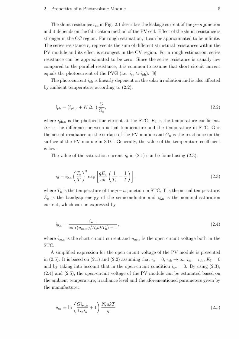
The shunt resistance rsh in Fig. 2.1 describes the leakage current of the p−n junction
and it depends on the fabrication method of the PV cell. Effect of the shunt resistance is
stronger in the CC region. For rough estimation, it can be approximated to be infinite.
The series resistance rs represents the sum of different structural resistances within the
PV module and its effect is strongest in the CV region. For a rough estimation, series
resistance can be approximated to be zero. Since the series resistance is usually low
compared to the parallel resistance, it is common to assume that short circuit current
equals the photocurrent of the PVG (i.e. isc ≈ iph). [8]
The photocurrent iph is linearly depenent on the solar irradiation and is also affected
by ambient temperature according to (2.2).
iph = (iph,n +KI∆T)G
Gn
, (2.2)
where iph,n is the photovoltaic current at the STC, KI is the temperature coefficient,
∆T is the difference between actual temperature and the temperature in STC, G is
the actual irradiance on the surface of the PV module and Gn is the irradiance on the
surface of the PV module in STC. Generally, the value of the temperature coefficient
is low.
The value of the saturation current i0 in (2.1) can be found using (2.3).
i0 = i0,n
(
Tn
T
)3
exp
[
qEg
ak
(
1
Tn
−1
T
)]
, (2.3)
where Tn is the temperature of the p−n junction in STC, T is the actual temperature,
Eg is the bandgap energy of the semiconductor and i0,n is the nominal saturation
current, which can be expressed by
i0,n =isc,n
exp (uoc,nq/NsakTn)− 1, (2.4)
where isc,n is the short circuit current and uoc,n is the open circuit voltage both in the
STC.
A simplified expression for the open-circuit voltage of the PV module is presented
in (2.5). It is based on (2.1) and (2.2) assuming that rs = 0, rsh → ∞, isc = iph, KI = 0
and by taking into account that in the open-circuit condition ipv = 0. By using (2.3),
(2.4) and (2.5), the open-circuit voltage of the PV module can be estimated based on
the ambient temperature, irradiance level and the aforementioned parameters given by
the manufacturer.
uoc = ln
(
Gisc,nGnio
+ 1
)
NsakT
q(2.5)

2. Properties of a Photovoltaic Module 6
2.2 Effect of Climate Conditions on the PV Module
The simulated I-U curve of NAPS NP190Gkg PV module, which is used in this thesis,
is shown in Fig. 2.3 at two different temperature and irradiance levels. The linear
depency of the short-circuit current on irradiance level was expressed mathematically
in (2.2) and it is also visible in this graph. The dashed curve crosses the y-axis almost at
the same point as the solid line, which means that the effect of ambient temperature on
short-circuit current is low, complying to the information given by (2.2). Respectively,
the dashed and solid lines cross the x-asis as pairs, which means that the open-circuit
voltage is affected more by ambient temperature than irradiance level.
0 5 10 15 20 25 30 35 400
2
4
6
8
10
12
Voltage (V)
Curr
ent
(A)
1.9 °C
40.0 °C
1400 W/m²
600 W/m²
Figure 2.3: Simulated I-U curve of the NAPS NP190GKg PV module
According to Fig. 2.3 and Ref. [8], it is reasonable to assume that the effect of
ambient temperature on short-circuit current is negligible. In this case, the short-
circuit current of the PV panel is solely determined by incident radiation. Thus, the
maximum value for the short-circuit current is found according to the maximum value
of incident radiation.
When the sunlight passes through the atmosphere, a part of the radiation is ab-
sorbed and scattered. On a clear day approximately 75% of the solar irradiation coming
from the sun passes through the atmosphere without scattering or absorbtion. This
part of the irradiation is called direct irradiance. Some of the scattered sunlight is
not scattered into space, but ends up on the surface of the earth. This part of the
radiation is called diffuse radiation. Route of the scattered sunlight might be quite
complicated. For example in snowy areas, sunlight might scatter first from the snow
and then rescatter from the atmospere to the PVG. All of the scattered components
are included in diffuse radiation. Sum of the direct irradiance and diffuse radiation is
called global irradiance. [11]
Scattering of the sunlight from the edge of a cloud causes significant increase in
diffuse radiation and further an increase in global radiation. This phenomenon is
called the cloud enhancement. During the cloud enhancement, global radiation might
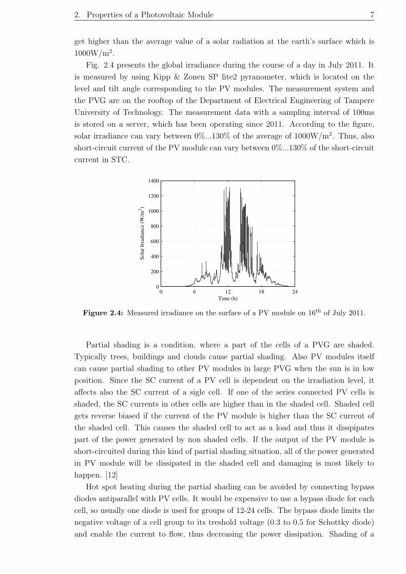
2. Properties of a Photovoltaic Module 7
get higher than the average value of a solar radiation at the earth’s surface which is
1000W/m2.
Fig. 2.4 presents the global irradiance during the course of a day in July 2011. It
is measured by using Kipp & Zonen SP lite2 pyranometer, which is located on the
level and tilt angle corresponding to the PV modules. The measurement system and
the PVG are on the rooftop of the Department of Electrical Engineering of Tampere
University of Technology. The measurement data with a sampling interval of 100ms
is stored on a server, which has been operating since 2011. According to the figure,
solar irradiance can vary between 0%...130% of the average of 1000W/m2. Thus, also
short-circuit current of the PV module can vary between 0%...130% of the short-circuit
current in STC.
0 6 12 18 240
200
400
600
800
1000
1200
1400
Time (h)
Sola
r Ir
radia
nce (
W/m
2)
Figure 2.4: Measured irradiance on the surface of a PV module on 16th of July 2011.
Partial shading is a condition, where a part of the cells of a PVG are shaded.
Typically trees, buildings and clouds cause partial shading. Also PV modules itself
can cause partial shading to other PV modules in large PVG when the sun is in low
position. Since the SC current of a PV cell is dependent on the irradiation level, it
affects also the SC current of a sigle cell. If one of the series connected PV cells is
shaded, the SC currents in other cells are higher than in the shaded cell. Shaded cell
gets reverse biased if the current of the PV module is higher than the SC current of
the shaded cell. This causes the shaded cell to act as a load and thus it disspipates
part of the power generated by non shaded cells. If the output of the PV module is
short-circuited during this kind of partial shading situation, all of the power generated
in PV module will be dissipated in the shaded cell and damaging is most likely to
happen. [12]
Hot spot heating during the partial shading can be avoided by connecting bypass
diodes antiparallel with PV cells. It would be expensive to use a bypass diode for each
cell, so usually one diode is used for groups of 12-24 cells. The bypass diode limits the
negative voltage of a cell group to its treshold voltage (0.3 to 0.5 for Schottky diode)
and enable the current to flow, thus decreasing the power dissipation. Shading of a

2. Properties of a Photovoltaic Module 8
single cell causes the whole group to be bypassed meaning that also the non shaded cells
in the group are bypassed and the output power of the PVG decreases by a large step.
Thus, the group size is a tradeoff between price and sensivity to partial shading.[13]
2.3 Limit Values of NAPS NP190GKg PV Module Output
Maximum and minimum values of the current, voltage and power of the PV module
output are needed in the design of a PV converter. The converter should be able to
control its input voltage between the minimum and maximum MPP voltages of the PV
module. Maximum value of the MPP voltage appears when the whole PV module is
evenly illuminated and when the temperature is low and irradiance high. Respectively,
the minimum value appears when the PV module is partially shaded so that only one
group of the series connected cells is not bypassed and when the temperature is high
and irradiance low.
The minimum and maximum values of NAPS NP190GKg PV module are of concern,
since it is used in this thesis. Electrical characteristics of the module given in the
manufacturer datasheet in STC are given in Table 2.1. These values are used in the
calculations later on.
Table 2.1: Electrical characteristics of NAPS NP190GKg PV Module in STC
Parameter Value
UOC,STC 33.1 VISC,STC 8.02 APMPP,STC 190 WUMPP,STC 25.9 VIMPP,STC 7.33 A
The internal connection of the PV cells inside NAPS NP190GKg PV module is
presented in Fig. 2.5. The module consist of 54 series connected cells, which are
divided into three groups, each of which has antiparallel bypass diode. These diodes
are located in a module junction box.
pvu
pvi
Figure 2.5: Internal connection of the PV cells inside NAPS NP190GKg PV module
The MPP voltage reaches its minimum value when two out of three of the bypass-
diode groups are shaded. In this situation, current flows through two bypass diodes
and 18 cells of non shaded group. Open-circuit voltage of a Si solar cell decreases by

2. Properties of a Photovoltaic Module 9
rate of 2.3mV/K when temperature increases[13]. If the effect of irradiance on OC
voltage is neglected, minimum MPP voltage UMPP,MIN can be approximated by (2.6).
UMPP,MIN =UMPP,STC − (TMAX − TSTC)NsKV
3− 2Ud, (2.6)
where UMPP,STC is the MPP voltage in STC, TMAX is maximum cell temperature, TSTC
is the cell temperature in STC, which is 25C, KV is the temperature coefficient of
the cell voltage and Ud is the forward voltage drop of the bypass diode. Minimum
MPP voltage is 5.8 V, when the following values are used: TMAX = 60C, Ns = 54,
Ud = 0.7V . This value is used in Chapter 3 as the minimum input voltage of the
converter.
Maximum output voltage of the PV module was found by substituting the measure-
ment data of the irradiance and the backplate temperature of NAPS NP190GKg PV
module to the simplified equation (2.5). The same measurement setup has been used
here as it was used to produce Fig. 2.4. Temperature was measured by using PT100
temperature sensor located on the back of the PV module. It was predicted, that the
maximum peak of the OC voltage would take place in the spring when temperature is
low and a peak in diffuse radiation would be formed due to cloud enhancement.
By studying the measurement data from June 2011 to May 2012, it was observed
that the highest peak in OC voltage and in glogal irradiance took place on 5th of April
2012. Measured irradiance during the course of that day is shown in Fig. 2.6. As it
is shown, the irradiance level fluctuates heavily and the peak takes place around noon,
caused most likely by the cloud enhancement.
0 6 12 18 240
200
400
600
800
1000
1200
1400
Time (h)
Sola
r Ir
radia
nce (
W/m
2)
Figure 2.6: Measured irradiance on the surface of PV module on 5th of April 2012.
An extended view of the global irradiance peak value is shown in Fig. 2.7. The
irradiance level stays above 1000W/m2 for several minutes, around 1300W/m2 for a
minute and around 1400W/m2 for several seconds. Backplate temperature of NAPS
NP190GKg PV module is presented in Fig. 2.8 measured at the same time as global

2. Properties of a Photovoltaic Module 10
irradiance. Backplate temperature is quite low and increases slowly. Actually the
temperature stays almost constant compared to irradiance during the measurement
period.
0 100 200 300 400 500 600 700 8000
200
400
600
800
1000
1200
1400
Time (s)
Sola
r Ir
radia
nce (
W/m
2)
Figure 2.7: Measured peak in the irradiance on the surface of PV module during the cloudpassing conditions.
0 100 200 300 400 500 600 700 8000.0
0.2
0.4
0.6
0.8
1.0
1.2
1.4
1.6
1.8
2.0
Time (s)
Tem
per
ature
(°C
)
Figure 2.8: Measured temperature on the back of PV module during the cloud passingconditions.
Open-circuit voltage in Fig. 2.9 was calculated by substituting the data of Fig. 2.7
and Fig. 2.8 to equation (2.5). As it is shown, OC voltage stays around 35 V during
the whole measurement period. Because this graph was achieved by the simplified
model that neglects the effect of shunt and series resistance, the maximum OC voltage
was also simulated by Matlab R© Simulink model based on (2.1). This model is already
verified to be valid for the same PV module in the prior research [12]. Temperature
of 1.9C and irradiance of 1400W/m2 were used in the simulation. As it is visible in
the simulated I-U curve of Fig. 2.10, maximum open-circuit voltage is 36.5V, which
is one volt higher than the value achieved by the simplified model. Simulated value is
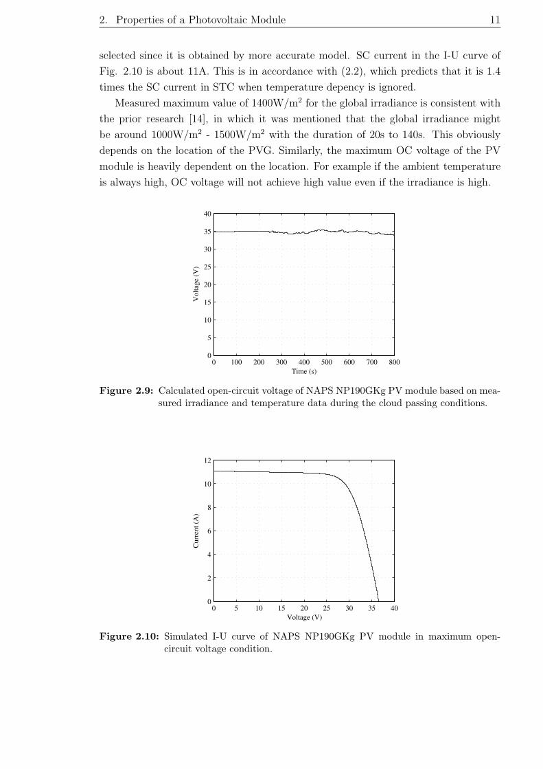
2. Properties of a Photovoltaic Module 11
selected since it is obtained by more accurate model. SC current in the I-U curve of
Fig. 2.10 is about 11A. This is in accordance with (2.2), which predicts that it is 1.4
times the SC current in STC when temperature depency is ignored.
Measured maximum value of 1400W/m2 for the global irradiance is consistent with
the prior research [14], in which it was mentioned that the global irradiance might
be around 1000W/m2 - 1500W/m2 with the duration of 20s to 140s. This obviously
depends on the location of the PVG. Similarly, the maximum OC voltage of the PV
module is heavily dependent on the location. For example if the ambient temperature
is always high, OC voltage will not achieve high value even if the irradiance is high.
0 100 200 300 400 500 600 700 8000
5
10
15
20
25
30
35
40
Time (s)
Volt
age
(V)
Figure 2.9: Calculated open-circuit voltage of NAPS NP190GKg PV module based on mea-sured irradiance and temperature data during the cloud passing conditions.
0 5 10 15 20 25 30 35 400
2
4
6
8
10
12
Voltage (V)
Curr
ent
(A)
Figure 2.10: Simulated I-U curve of NAPS NP190GKg PV module in maximum open-circuit voltage condition.

12
3. OPERATION OF A BOOST-POWER-STAGE
CONVERTER
In the grid connected solar energy systems, one common approach is to use double-
stage conversion, in which there is the single-phase or three-phase inverter after the
boost-power stage converter. In this way, greater variances in input voltage can be
tolerated and the maximum input voltage can be smaller compared to the single-stage
conversion consisting only the inverter [13]. It is also possible that the losses caused
by partial shading are smaller due to less series connected PV modules [12].
Other benefits of the boost topology in photovoltaic applications are that the input
current is continuous and that blocking diode is included in the topology so no addi-
tional diode is needed. Blocking diode is needed to prevent current from flowing back
to the PVG during the night or other times of low irradiation. [15]
The maximum power point tracking is carried out in the DC/DC converter and the
DC/AC converter controls its output current and input voltage as the grid connection
requires. The DC/DC converter can operate at open or closed loop. In the open loop
operation, duty ratio is directly controlled by MPPT. In the closed loop operation,
MPPT-algorithm calculates the input voltage reference, which is then used as a ref-
erence value for the closed loop controller of the converter. The block diagram of the
double-stage inverter is presented in Fig. 3.1 [16]
MPPT
DC-DC DC-ACPVGrid
pvi ref
pvu
pvu
in,invu gridi
Figure 3.1: Double-Stage Inverter [16].
In this thesis, the DC/DC converter of the double-stage conversion scheme is imple-
mented by taking into account that it is a part of the double-stage inverter presented
above. This means that the effects of PVG and inverter on the dynamics of the DC/DC
converter are taken into account. Closed-loop control scheme is used and the reference
value for the controlled variable is provided manually, which means that the MPP
tracking is not implemented.
Controlling of the input-side variable is compulsory for maximizing power transfer
[17]. Output current of the PVG is directly proportional to the irradiance, which
varies in large scale and fast. Controlling of the PVG output current thus requires fast
3. Operation of a Boost-Power-Stage Converter 13
dynamics to follow the MPP and it could easily lead to saturation of the controller.
On the other hand, the change in irradiance only slightly affects on the output voltage
of the PVG. Instead, it is directly proportional on the temperature, which has slow
dynamics and hence the output voltage control of the PVG is preferred. [15]
Based on this information, input-voltage-based feeback control is implemented in
the DC/DC converter. As inverter controls its input voltage, it behaves as a voltage
type load for the DC/DC converter. This means that the DC/DC converter in this
application should be considered as current-fed current output(CF-CO) converter.
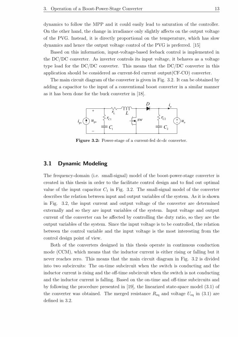
The main circuit diagram of the converter is given in Fig. 3.2. It can be obtained by
adding a capacitor to the input of a conventional boost converter in a similar manner
as it has been done for the buck converter in [18].
pvi
Lr L
D
oupvu
oi
C1r
1C
C2r
2C
Figure 3.2: Power-stage of a current-fed dc-dc converter.
3.1 Dynamic Modeling
The frequency-domain (i.e. small-signal) model of the boost-power-stage converter is
created in this thesis in order to the facilitate control design and to find out optimal
value of the input capacitor C1 in Fig. 3.2. The small-signal model of the converter
describes the relation between input and output variables of the system. As it is shown
in Fig. 3.2, the input current and output voltage of the converter are determined
externally and so they are input variables of the system. Input voltage and output
current of the converter can be affected by controlling the duty ratio, so they are the
output variables of the system. Since the input voltage is to be controlled, the relation
between the control variable and the input voltage is the most interesting from the
control design point of view.
Both of the converters designed in this thesis operate in continuous conduction
mode (CCM), which means that the inductor current is either rising or falling but it
never reaches zero. This means that the main circuit diagram in Fig. 3.2 is divided
into two subcircuits: The on-time subcircuit when the switch is conducting and the
inductor current is rising and the off-time subcircuit when the switch is not conducting
and the inductor current is falling. Based on the on-time and off-time subcircuits and
by following the procedure presented in [19], the linearized state-space model (3.1) of
the converter was obtained. The merged resistance Req and voltage Ueq in (3.1) are
defined in 3.2.

3. Operation of a Boost-Power-Stage Converter 14
diLdt
= −Req
LiL +
1
LuC1 +
rC1
Liin −
D′
Luo +
Ueq
Ld
duC1
dt= −
1
C1
iL +1
C1
iin
duC2
dt= −
1
rC2C2
uC2 +1
rC2C2
uo
uin = −rC1iL + uC1 + rC1iin
io = D′iL +1
rc2uC2 −
1
rC2
uo − Iind,
(3.1)
Req = rC1 + rL +DrSW +D′rD
Ueq = [rD − rSW] Iin + Uo + UD,(3.2)
The linearized state-space model in (3.1) can also be presented in the matrix form
as in (3.3) and (3.4).
diLdt
duC1
dt
duC2
dt
=
−Req
L
1L
0
− 1C1
0 0
0 0 − 1rC2C2
iL
uC1
uC2
+
rC1
L−D′
L
Ueq
L
1C1
0 0
0 1rC2C2
0
iin
uo
d
(3.3)
[
uin
io
]
=
[
−rC1 1 0
D′ 0 1rc2
]
iL
uC1
uC2
+
[
rC1 0 0
0 − 1rC2
−Iin
]
iin
uo
d
(3.4)
Linearized state-space in (3.3) and (3.4) is now in the standard state-space form
as given in (3.5). Inductor current and capacitor voltages are state variables, input
current, duty ratio and output voltage are the input variables as well as input voltage
and output current are output variables, respectively. The standard linearized state-
space representation (3.5) can be transformed in to the frequency domain by Laplace
transform, which yields (3.6).
du(t)
dt= Ax(t) +Bu(t)
y(t) = Cx(t) +Du(t)
(3.5)
sX(s) = AX(s) +BU (s)
Y (s) = CX(s) +DU (s)(3.6)
3. Operation of a Boost-Power-Stage Converter 15
Solving the relation between input and output variables from (3.6) yields
Y (s) = (C(sI−A)-1B+D)U (s) = GU(s), (3.7)
MatrixG in (3.7) contains the transfer functions of the converter. Thus, (3.7) describes
how to calculate the transfer functions when linearized state-space matrices are solved.
Transfer function set of the boost-power-stage converter are as given in 3.8.
[
uin
io
]
=
[
Zin-o Toi-o Gci-o
Gio-o −Yo-o Gco-o
]
iin
uo
d
(3.8)
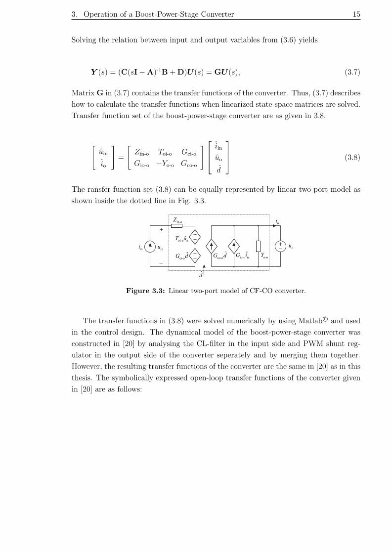
The ransfer function set (3.8) can be equally represented by linear two-port model as
shown inside the dotted line in Fig. 3.3.
ini ouinu
oiin-oZ
oi-o oˆT u
co-oˆG d io-o in
ˆG i o-oY
d
ci-oˆG d
Figure 3.3: Linear two-port model of CF-CO converter.
The transfer functions in (3.8) were solved numerically by using Matlab R© and used
in the control design. The dynamical model of the boost-power-stage converter was
constructed in [20] by analysing the CL-filter in the input side and PWM shunt reg-
ulator in the output side of the converter seperately and by merging them together.
However, the resulting transfer functions of the converter are the same in [20] as in this
thesis. The symbolically expressed open-loop transfer functions of the converter given
in [20] are as follows:

3. Operation of a Boost-Power-Stage Converter 16
Zin-o =1
LC1
(Req − rC1 + sL) (1 + srC1C1)1
∆
Toi-o =D′
LC1
(1 + srC1C1)1
∆
Gci-o = −Ueq
LC1
(1 + srC1C1)1
∆
Gio-o = −D′
LC1
(1 + srC1C1)1
∆
Gco-o = −Iin
(
s2 − s
(
D′Ueq
LIin−
Req
L
)
+1
LC1
)
1
∆
Yo-o =D’2
L·
s
s2 + sReq
L+ 1
LC1
+sC2
1 + srC2C2
,
(3.9)
where
∆ = s2 + sReq
L+
1
LC1
, (3.10)
Steady-state duty cycle D of the converter is as given in (3.11).
D =(rL + rD) Iin − Uin + Uo + UD
(rD − rSW) Iin + Uo + UD
, (3.11)
The closed-loop transfer functions of the input-voltage-controlled converter were also
solved in [20] based on the control-block diagrams in Fig. 3.4 and Fig. 3.5 and are as
follows
Zin-c =uin
iin=
Zin-o
1− Lin
Toi-c =uin
uo
=Toi-o
1− Lin
Gri =uin
urefin
= −Lin
1− Lin
·1
Gse-in
Gio-c =io
iin=
Gio-o
1− Lin
−Lin
1− Lin
Gio-∞
Yo-c =iouo
=Yo-o
1− Lin
−Lin
1− Lin
Yo-∞
Gro =iourefin
= −Lin
1− Lin
·Gco-o
Gci-o
·1
Gse-in
,
(3.12)
where

3. Operation of a Boost-Power-Stage Converter 17
Lin = Gse-inGcGaGci-o,
Gio-∞ = Gio-o −Zin-oGco-o
Gci-o
, Yo-∞ = Yo-o +Toi-oGco-o
Gci-o
,(3.13)
where Lin is called input-voltage loop gain, Gse-in is the input-voltage sensing gain, Gc
is the input-voltage controller transfer function, Ga is the modulator gain, Gio-∞ is ideal
forward current gain and Yo-∞ is the ideal output admittance, respectively.
in-oZ
oi-oT
ci-oG
aG cG
se-inG
ini
ou inu
ref
inud
Figure 3.4: Control-block diagram of input dynamics [20].
io-oG
o-oY
co-oG
aG cG
se-inG
ini
ou oi
ref
inud
inu
Figure 3.5: Control-block diagram of output dynamics [20].
Output power of a single-phase inverter fluctuates at twice the grid fequency, which
causes a ripple component at the input voltage of the inverter. The requency of the
ripple is also twice the grid frequency which is assumed to be 100 Hz in this thesis. If
this ripple voltage ends up to the input side of the dc-dc converter, the voltage of the
PV module will fluctuate around MPP reducing the energy yield.
Prevention of the output power fluctuation from affecting the input power is called
power decoupling. Common power decoupling method is to add large capacitor parallel
to the PV module or to the output of the DC/DC converter. Greatest drawback in
this method is that the high-capacitance electrolytic capacitors, which are typically
used, have limited lifetime and high price. Also various more complicated methods to
implement power decoupling in the PV application are presented in the literature [21].
Transfer function Toi-c describes the relation between input and output voltages of
the converter meaning that if Toi-c is smaller than unity, the converter will prevent
output voltage ripple from affecting the input voltage. According to (3.12), Toi-c de-
pends on the loop gain meaning that it can be affected by controller design. The higher

3. Operation of a Boost-Power-Stage Converter 18
the controller gain, the greater the attenuation. Thus, the controller design should be
implemented so that the loop gain is high enough at the frequency of 100 Hz. Small
input capacitor can be used if the fluctuating power is handeled by the capacitor in the
output of the dc-dc converter. The value of the output capacitor can be lower because
the ripple in the output can be higher due to the attenuation of the converter. Great
benefit is also that no additional components are needed as in some of the presented
methods in [21].
3.2 The Effect of Nonideal Source
The closed-loop transfer functions of the converter in (3.9) were calculated by assuming
that the source and load are ideal. However, PVG is not ideal and thus its effect on
the converter dynamics shall be taken into account. Nonideal source can be modelled
by adding admittance YS parallel to the input current source as shown in Fig. 3.6.
inSi ouinu
oiin-oZ
oi-o oˆT u
co-oˆG d io-o in
ˆG i o-oY
d
ci-oˆG dSY
ini
Si
Figure 3.6: Linear two-port model of CF-CO converter with nonideal source.
Now, the input current of the converter is the input current iinS subtracted by the
current through the admittance iS. When this new input current is substituted to
(3.8), the source affected transfer functions of the converter (3.14) can be solved as
instructed in [20].
[
uin
io
]
=
[
ZSin-o T S
oi-o GSci-o
GSio-o −Y S
o-o GSco-o
]
iinS
uo
d
=
Zin-o
1 + YsZin-o
Toi-o
1 + YsZin-o
Gci-o
1 + YsZin-o
Gio-o
1 + YsZin-o
−1 + YsZin-oco
1 + YsZin-o
Yo-o
1 + YsZin-∞
1 + YsZin-o
Gco-o
iinS
uo
d
(3.14)
where Zin-oco denotes the input impedance of the converter when the output of the
converter is open-circuited and Zin−∞ denotes the so called ideal input impedance
given in Equations (3.15) and (3.16), respectively.
Zin-oco = Zin +GioToi
Yo
, (3.15)

3. Operation of a Boost-Power-Stage Converter 19
Zin−∞ = Zin −GioGci
Gco
(3.16)
In the case of very low admittance YS, the current through the admittance would
be negligible and the situation would be as in Fig. 3.3. Because the admittance is
the inverse of impedance, this situation would mean that the output impedance of
the source would be high. As it was discussed in the previous chapter, the output
impedance of the PV module is high when the output voltage of the PV module is low.
This means that the effect of the PV module on the converter dynamics is more severe
in the CV region than in the CC region of the PV module.
The final closed-loop model of the converter can be solved by first calculating the
open-loop transfer functions of the converter as in (3.7), then adding the effect of the
PV module by using (3.14) and finally by solving the closed-loop transfer functions by
(3.12).

20
4. CONVERTER DESIGN
In this chapter, two different boost-power-stage converters are designed. First one
is named as Converter CM, because its design is based on the conventional design
methods presented in [3] and [4]. The second converter is named as Converter NM,
because its design is based on the charasteristics of the solar panel during the different
climatic conditions including peaks in incident radiation. In [3], the designed converter
is an interleaved boost, whereas in [4] it is a three-level boost converter. In this thesis,
the design is based on a basic boost converter but comparison with the aforementioned
publications is relevant since the basic principles in component sizing are the same.
4.1 Maximum Input Current and Voltage
Sizing factor (SF ) is the ratio of solar inverter nominal power Pnom to the dc power
of a PVG in STC PPVG-STC as in (4.1). Depending on the source, Pnom might be
input [22] or output [14] power of the inverter. Input power is used in this thesis.
Inverter might have one or two conversion stages, in which case both of the conversion
stages must have the same power rating. So in the case of double-stage conversion,
input power of a solar inverter is also the input power of a DC/DC converter. When
0 < SF < 1, the inverter is undersized and for SF > 1, the inverter is oversized
compared to the PVG. Optimal SF value has been studied widely, and there are various
publications concerning it [22],[14],[23]. The main factors that affect the optimal value
of SF are ambient temperature and irradiance patterns, incentives, protection method
and efficiency of the inverter.
SF =Pnom
PPVG-STC
(4.1)
Protection of a solar inverter can be implemented in several ways. One way is
to shut down the inverter immediately when over-current is detected. Other way is to
have a time delay before entering into protection mode and the power can be limited to
acceptable level, e.g to nominal power. Protection can also be based on the temperature
measurement of power semicodunctors. The immediate shutdown decreases energy
yield substantially if the inverter is undersized and incident radiation fluctuates heavily
as in Fig. 2.3. On the other hand, if time delay and power limiting are used, it is
possible to achieve greater energy yield by the same inverter. Power limiting can be
done by moving the operation point away from the MPP by changing the input voltage
to a higher level. [22]

4. Converter Design 21
The value of 0.7 for SF is used in this thesis since it is the widely used rule-of-
thumb and thus represents the typical case. It is also assumed that the protection
of the converter is implemented by limiting the output power to the level of nominal
power. By using the sizing method presented in [3] and [4], the maximum input current
of the converter for NAPS NP190Gkg PV module would be as follows:
IIN,MAX =PPVG-STCSF
UMPP,MIN
(4.2)
The maximum input current is 22.9 A when the values given in Chapter 2 and (4.2)
are used. On the other hand, the maximum current that is possible to get from the
NAPS NP190Gkg PV module in any climate condition is about 1.4 times the short-
circuit current in STC, which equals to 11.2 A. This is the input current value used in
the new design method. The difference between the current values of these two design
methods is remarkable and it would be even greater if the higher value of SF would
be used. For example by using unity SF , which is also a commonly used value, the
maximum input current would be 32.8 A [22]. It is also essential to remember that
by using the conventional design method, the output power of the converter is limited
to be lower than the nominal output power of the PV module, whereas in the new
design method the converter is designed to handle the maximum output power of the
PV module.
In Chapter 2, the maximum OC output voltage of NAPS NP190Gkg PV module
was found to be 36.5 V. Even if the output voltage mainly stays below this value when
operating at the MPP, the converter should be able to handle the OC voltage as well.
By adding some safety margin, the voltage rating of the components in both of the
converters should be 50 V. Output voltage of the converter was selected to be 40V,
because it is higher than the highest input voltage but still safe to handle. It should
be noted that the input voltage of the inverter, which is connected to the grid, should
have higher input voltage than the peak value of the grid voltage. However, the results
presented in this thesis are also valid in the converters with higher voltage levels.
4.2 Inductor Design
First of all, the minimum value for the inductance to produce specified amount of
current ripple is defined. Inductor voltage can be approximated by (4.3).
uL = LdiLdt
≈ L∆iL,pp∆t
, (4.3)
where uL is the inductor voltage, L is the inductance, iL is the inductor current, ∆iL,pp is
the inductor current peak-to-peak ripple value and ∆t is the rising time of the inductor
current, which is on-time of the switch. During the on-time, the inductor voltage equals
to the input voltage in boost converter. The expression for inductor current ripple can

4. Converter Design 22
be solved by substituting (3.11) without parasitics into (4.3) yielding
∆iL,ppL = uL∆t = UinDTs =Uin
fs−
U2in
fsUo
(4.4)
The inductor current ripple is at its highest value when the input voltage is half the
output voltage, which can be found by calculating the partial derivative of (4.4) in
respect to the input voltage. By substituting this information back to (4.4) and by
solving the inductance, the minimum value of the inductance is found:
L =Uo
4∆iL,ppfs(4.5)
Core material was selected to be Metglas, which is made of amorphous metal having
high saturation flux density and low core losses. Maximum inductor current ripple was
set to be 10% of the maximum input current. The maximum peak flux density was set
to be 90% of the saturation flux density of the core. These selections were made to be
consistent with [3] and [4]. Values that were used as a specification for the inductor
design are presented in Table 4.1.
Table 4.1: Inductor Design Specification
Symbol Description Value Unit
J Current density 500 A/cm2
K Window utilization factor 0.4BMAX Maximum peak flux density 1.4 T
Core selection was based on the core area product WaAc, which is defined in (4.6).
The complete derivation of this equation is presented in [24]
WaAc =LI2L,p10
4
BmaxJK, (4.6)
where IL,p is the peak value of the inductor current. With 10% ripple, the inductor
current peak value is 1.05 times maximum input current. L is the minimum inductance
value according to (4.5). The result of (4.6) is in cm4, which is the same unit as in
Metglass datasheets. Few metglass microlite toroidial cores with distributed airgap
were selected as core candidates. Cores of Metglass C-series that were used in [3] and
[4] are too large to be used in this application.
After core selection, the preliminary number of turns was calculated by using (4.7).
It is called preliminary, because the permeability of the core decreases when the mag-
netic flux in the core increases, which is dependent on the DC current through the
winding and on the number of turns. This means that selecting the number of turns is
an iterative process. Nominal relative permeability of 245 given in the datasheet [25]

4. Converter Design 23
was selected to be the preliminary relative core permeability. [4]
Ni =
√
Llmµ0µeAe
, (4.7)
where lm is the core magnetic path length, µ0 is the permeability of free space, µe
is the relative core permeability and Ae is the cross-sectional area of the core. The
preliminary number of turns was substituted in (4.8), which gives the magnetic field
strength in Oersteds (Oe).
H =0.4NIdc
lm, (4.8)
where N is the number of turns and Idc is the dc bias current through the coil. In this
case, it equals to IIN,MAX
By using the graph that is presented in the Mircolite datasheet, where core perme-
ability is presented as a function of magnetic field strength, new and more accurate
value for the core permeability was found. Aforementioned steps should be repeated
as many times as it is required to find the value of the core permeability. In practice,
this means that last two iteration rounds must lead to the same number of turns. In
this case three iteration rounds was sufficient. Also higher temperature decreases the
inductance of the inductor but this was not taken into account in the calculations. [25]
Required cross-sectional area Aw of the wire was calculated directly from the current
density J specification given in Table 4.1 as
Aw =IL,pJ
(4.9)
Calculated cross-sectional area was then rounded to the closest standard value. Now
the dc resistance RDC of the wire can be calculated as
RDC = ρlwAw
, (4.10)
where ρ is the conductivity of wire material, lw is the length of the wire. Six
inductors was designed based on Equations (4.1) - (4.10) and the results are presented
in Table 4.2. First three rows are calculated by using the conventional design method
and three latter rows are calculated by using the new design method.
As it is visible from the Table 4.2, the conventional design method leads to lower
inductance value and to higher wire gauge than the new design method. On the
other hand, DC resistance of the inductors that are designed by using the conventional
method are lower, due to the less number of turns with larger wire gauge. This leads to
lower power losses as presented later. MP3310LDGC and MP2510LDGC were selected,

4. Converter Design 24
Table 4.2: Results of the inductor design
Core Vcore (cm3) IIN,MAX (A) L (µH) N Rdc (mΩ) Aw (mm2)
MP3210LDGC 3.52 22.9 43 20 6 4MP3310LDGC 5.34 22.9 43 13 4 4MP3505MDGC 5.34 22.9 43 13 4 4
MP2610LDGC 2.48 11.2 89 25 11 2.5MP2510LDGC 1.89 11.2 89 32 14 2.5MP2310MDGC 2.38 11.2 89 25 11 2.5
because they were the only cores in Table 4.2 available from the manufacturer.
Power losses of the inductor are distributed within the core and winding. Thus, the
total power loss consists of core and copper losses. Core losses are the sum of hysteresis,
eddy current and residual losses [26]. Copper losses can be further divided into the
losses caused by the direct current flowing through the resistance of the winding and
into the losses caused by the alternating current due to skin and proximity effects.
At high frequencies, the current density is higher in the outer layer of the conductor.
This phenomenon is called skin effect. Alternating current flowing through a conductor
causes traverse field into other conductor that is located next to it. This phenomenon
is called proximity effect. The losses caused by alternating current was calculated by
using the methods presented in [4], but since its share of the total power loss was only
about 0.5%, it was omitted from the loss calculation. The equations needed to calculate
the total power loss of the inductor are presented next. The peak value of the AC flux
BAC,PEAK can be calculated as given in (4.11) [4].
BAC,PEAK =µ0µreal∆iL,ppN
2lm, (4.11)
where µreal and N are final values from the iterative inductor design and the rest are
predefined quantities. The result is substituted to (4.12) in order to find the value for
inductor core loss PCORE.
PCORE = m(
275B2.6AC,PEAKfs + 0.114B2
AC,PEAKfs)
, (4.12)
where m is the mass of the core. Eq. (4.12) is given in the Microlite datasheet [25]
including all of the aforementioned core loss components. The DC part of the copper
losses can be simply calculated by (4.13).
PCU,DC = I2DCRDC, (4.13)
where IDC is the direct current flowing through the winding, which is the input current
in the case of a boost-power-stage converter.

4. Converter Design 25
By summing the core and copper losses and by neglecting the copper losses caused
by alternating current, the total power loss is as given in (4.14).
PTOT = PCORE + PCU,DC (4.14)
The power loss calculation was made for both of the selected inductors in STC.
The results are presented in Table 4.3. As it is shown, the conventional design method
leads to a larger core, and thus also higher core loss than the new design method. On
the other hand, the copper loss is lower due to the less number of turns with larger
wire gauge. By using these values and cores, it seems that total power losses in STC
are higher when the new design method is used.
Table 4.3: Results of power loss calculation in STC
Core PCORE (W) PCU,DC (W) PTOT (W)
MP3310LDGC 0.50 0.27 0.77MP2510LDGC 0.26 0.88 1.14
According to Table 4.3, if the cost is the most important factor, then the new design
method should be used. But if the efficiency is the most important factor, then the
conventional design method might be better option.
The inductors were built based on the design results presented in Table 4.2 by
using the selected cores MP3310LDGC and MP2510LDGC. The winding of the 43-µH
inductor was divided into two parellel wires with the wire diameter of 1.6mm, because
the wire thicker than 1.8mm was not available from the distributor. It was also easier
to wind two thin wires instead of one thick wire. The inductance value of both of the
inductors was measured to verify the design. The value of the inductance was measured
by the means of the frequency response analyser Model 3120 of Venable Instruments
with an impedance measurement kit.
The measurement setup is presented in Appendix A. 12V/120Ah lead acid bat-
tery was used to produce high enough bias current through the inductor winding and
Chroma DC electric load was used to keep the bias current constant. The impedance
was measured with four different bias current values. The value of the inductance
was found by fitting the impedance graph of the RL circuit model to the measured
impedance graph.
The inductance measurements revealed that the inductance value dropped steeply as
a function of bias current, steeper than it was predicted in the datasheet. Two similarly
designed inductors were connected in series to get enough inductance and this solution
was also used in the converter prototypes. The measured and fitted impedance curves
of the series connected inductors are presented in Appendix A and the resulting values
of the inductances are presented in Table 4.4 and Table 4.5, respectively.

4. Converter Design 26
Table 4.4: Measurement from 89-µH inductor
Measurement current (A) Resistance (mΩ) Inductance (µH)
2.6 19.7 173
7.33 19.7 120
7.89 19.7 110
11 19.7 68
Table 4.5: Measurement from 43-µH inductor
Measurement current (A) Resistance (Ω) Inductance (µH)
2.6 6.4 85
7.33 6.4 72
7.89 6.4 69
23 6.4 38.2
As it is shown in Table 4.4, the inductance value of the 89-µH inductor is still not as
large as it was designed to be when the DC current is 11A. On the other hand, when
the DC current is 2.6A, inductance is much larger than expected. The inductor core
with an air gap might give less variation on inductance. That might be one of the
reasons, why such cores are commonly used in power converters. Such an alternative
for the core would have been Microlite 100u serie of Metglass.
The current values of 2.6A, 7.33A and 7.89A in Table 4.4 corresponds the operating
points, which are used in the frequency response measurements presented in Chapter
5. The measured inductance values are substituted to the model to fit the predicted
frequency responses to the measurements. As the inductance is larger than the desired
value of 89-µH at the operating points that are used in the measurements, the inductor
is adequate for the purposes of this thesis. Similar observations can be made on the
43-µH inductor based on Table 4.5 as for the 89-µH inductor.
4.3 Selection of MOSFET and Diode
In this thesis, the selection of the power semiconductors for the converter prototypes
was made as follows: First, a group of component cadidates was selected by their
voltage and current ratings, case type and availability. Then the component with the
lowest total power loss was selected from the group. As it was mentioned in the previous
chapter, the minimum voltage rating for the components in both of the converters was
specified to be 50 volts. The power switch was selected to be MOSFET, since it is the
best option for the used switching frequency and power range. The Schottky diode
was selected, because it has low forward voltage drop and negligible reverse recovery
loss even though it has larger reverse leakage current than the silicon pn-junction diode
[27].

4. Converter Design 27
The typical waveforms of the driver output voltage udri, inductor current iL, MOS-
FET current isw and diode current id are presented in Fig. 4.1. Inductor current flows
through the switch when it is on and through the diode when the switch is off.
LI
LI
LI
SDT ' SD T
driu
swi
di
Li
,L ppiD
,L ppiD
maxI
minI
Figure 4.1: Current waveforms in semiconductors.
The root mean square (RMS) value of the switch current Isw,rms can be calculated
as given in (4.15) based on the current waveform presented in Fig. 4.1 [19]. The
replacement of the duty ratio D in (4.15) by the complement of the duty ratio D′
yields to the RMS value of the diode current Id,rms as presented in (4.16).
Isw,rms = IL√D
√
1 +1
3
(
∆iL,pp2IL
)2
, (4.15)
Id,rms = IL√D′
√
1 +1
3
(
∆iL,pp2IL
)2
, (4.16)
where IL is the average value of the inductor current, which equals to the input current
of the boost-power-stage converter. D′ is the complementary duty ratio. The peak-to-

4. Converter Design 28
peak ripple of the inductor current ∆iL,pp can be solved from (4.4) yielding
∆iL,pp =UinDTs
L, (4.17)
where D is the duty cycle at the operation point where the RMS value of the current
is determined. The power loss of the semiconductor is quadratically dependent on the
RMS value of the current, which means that higher current produces higher loss. It
was stated in [3] that both of the semiconductors produce the highest loss when the
input voltage of the converter is in its minimum value. Small value of input voltage
means that the duty cycle has a large value and the complementary duty cycle D′ is
has a small value. The current waveforms in Fig. 4.1 corresponds to this situation.
According to (4.15), the RMS value of the current is heavily affected by the duty
cycle and average inductor current but the effect of inductor current ripple is not that
significant. If the average inductor current, i.e. the input current of the converter, is
constant, the RMS value of the current is mainly determined by the duty cycle. This
is a realistic assumption when operating in the CC region of the PV module. In the
case of a large value of D and a small value of D′, the power loss of the switch is higher
than the power loss of the diode. Respectively, if D has a small value and D′ has a
large value, the power loss of the diode is higher than the power loss of the switch.
The power loss of the diode increases when the duty ratio decreases, which means
that the input voltage of the converter, i.e. the output voltage of the PV module
increases. This is valid in the CC region and in the MPP but not anymore in CV
region, since the output current of the PV module starts to decrease. This means that
the power loss of the diode increases up to the MPP and starts to decrease if the voltage
is still increased. The diode power loss was calculated at different operation points of
the curve in Fig. 2.10 and it was verified that the maximum power loss of the diode
occurs at the MPP.
As a summary, the MOSFET power loss should be calculated at the minimum input
voltage and the power loss of the diode should be calculated at the MPP. The power
losses of Converter NM was calculated this way. The power losses of Converter CM
were calculated in the minimum input voltage for both of the semiconductors. The
calculated RMS current values of both of the design methods are presented in Table
4.6.
Table 4.6: Calculated RMS currents of the switch and diode
IIN,MAX (A) Isw,rms (A) Id,rms (A)
22.9 21.3 8.711.2 10.4 8.7
The current values obtained according to the conventional design method are pre-
sented in the first row of Table 4.6. The current values obtained according to the new
design method are presented in the second row, respectively. As it can be seen, there

4. Converter Design 29
is a significant difference in the RMS current of the switch between the two design
methods. Surprisingly, the diode RMS current became the same in both of the design
methods. Reason for this is that the higher input current is used in the conventional
design method but the diode current is calculated at the same operation point as the
current of the switch.
Now when the RMS values of the currents through the semiconductors are known,
the power losses can be approximated. The power loss calculations of the switch are
based on [28] and the detailed derivation of (4.18)-(4.26) can be found from there. The
total power loss Psw,tot of MOSFET switch is the sum of conduction losses Psw,sw and
switching losses Psw,c [28].
Psw,tot = Psw,c + Psw,sw (4.18)
MOSFET power switch conducts during the on-time. It can be modelled as a
resistor Rds,on. Resistance of Rds,on is given in the datasheet being dependent on the
drain-souce voltage and junction temperature. When the resistance and current is
known, the power loss during on-time can be estimated as follows
Psw,c = Rds,onI2sw,rms, (4.19)
In reality, the power switch turns on and off in finite time, introducing power losses.
The switch-on process of MOSFET can be divided into two parts: During the first
part, the drain-source voltage is the same as during the off-time and the drain current
is rising. This time period is called the current rise time tri given in the datasheet.
During the second part, the current is in the level defined by the other circuit elements
and the drain-source voltage is falling. This time period is called voltage fall time tfu
and it can be calculated as presented in (4.20)-(4.22). The voltage fall time is further
divided into two parts tfu1 and tfu2 since the drain-source voltage is approximated to
have two linear slopes. The idea is to take into account the non-linear behavior of the
drain-source voltage by simpification [28].
tfu =tfu1 + tfu2
2(4.20)
tfu1 = (Uo −RdsId,on)Rg
Cgd1
Udr − Uplateau
, (4.21)
where Uo is the output voltage of the converter, Rg is the gate resistor, Cgd1 is the
capacitance value of Crss read from the datasheet when Uds = Uo, Udr is the output
voltage of the driver circuit and Uplateau is the plateau voltage, which is also given in

4. Converter Design 30
the datasheet [28]. The second part of the voltage can be given as follows
tfu2 = (Uo −RdsId,on)Rg
Cgd2
Udr − Uplateau
(4.22)
where Cgd2 is the capacitance value of Crss given in the datasheet when Uds = Uo/2.
The switch-off process of MOSFET corresponds to the switch-on process in the reverse
order and so the time period tru during which the drain current is constant and drain-
source voltage is rising can be calculated as in (4.23)-(4.25). The other part of the
switch-off period is called current fall time tfi also given in the datasheet [28].
tru =tru1 + tru2
2, (4.23)
tru1 = (Uo −RdsId,on)Rg
Cgd1
Uplateau
(4.24)
tru2 = (Uo −RdsId,on)Rg
Cgd2
Uplateau
(4.25)
The switching losses can be calculated according to the defined switch-on and switch-off
events as given in (4.26).
Psw,sw = UoIdrain,ontri + tfu
2fs + UoIdrain,off
tru + tfi2
fs, (4.26)
where Idrain,on is the drain current in the beginning of tfu time period and Idrain,off is the
drain curren in the beginning of tfi time period [28].
The following criteria was used to select a group of power switch candidates: Max-
imum voltage rating at least 50V, maximum current ratings as given in Table 4.6, a
case that is easy attach to a heat sink and the switch should also be available from
the component distributors. The power loss calculations of the MOSFET candidates
for the converter designed by using the new design method are presented in Table 4.7.
The worst-case junction temperature was selected to be 100C as proposed in [27].
As it is shown in Table 4.7, IPA057N06N3 has lowest total power loss and thus
it was selected to the converter which was designed by using the new design method.
Similar comparison was also made for the converter that was designed by using the
conventional design method leading to the same MOSFET as with the new design
method. Thus, IPA057N06N3 was used in both of the converters with calculated total
power loss of 4.7 W by using the conventional design method and 2.6 W by using the
new design method. These values were used in the thermal design. Note that if more

4. Converter Design 31
Table 4.7: Results of MOSFET power loss calculation
Component Psw,c (W) Psw,sw (W) Psw,tot (W)
STD30NF06 2.9 3.6 6.5SI7478DP 0.9 4.0 4.9FDP42AN15A0 6.7 1.2 7.9IPD400N06N 5.2 1.5 6.7IPA057N06N3 0.7 1.9 2.6STP16NF06L 11.8 1.5 13.3IPD250N06N3 3.0 0.2 3.2
detailed component optimization would be used, the result might be quite different
than in this case. For example, the cost of the component might be included to the
optimization and a greater group of component candidates could have been evaluated.
Schottky diodes turns on and off faster than p−n junction diodes and have negligible
reverse recovery loss [27]. For this reason, the total power loss of the diode Pd,tot was
calculated by taking account only the conduction loss Pd,cond and the power loss caused
by reverse leakage current during the diode off time Pd,rev as follows
Pd,tot = Pd,cond + Pd,rev (4.27)
The conduction loss of the diode can be calculated as defined in (4.28), which has also
been used in [3].
Pd,c = Id,rmsUd, (4.28)
where Id,rms is the RMS current of the diode given in Table 4.6 and Ud is the forward
voltage drop of the diode given in the datasheet. Reverse current loss Pd,rev can be
calculated as presented in (4.29) [29].
Pd,rev = Ud,revId,revD, (4.29)
where Ud,rev is the reverse voltage, which in this case equals to output voltage of the
converter Uo, Id,rev is the reverse leakage current of the diode given in the datasheet
and D is the duty cycle of the MOSFET. Multiplication with D is needed, because the
reverse current loss occurs only during the off time, which occurs during the on time of
the switch. If the conventional design method would be used, the input voltage would
be 5.8 V meaning that the duty cycle is 0.86. If the new design method would be used,
input voltage would be 28.5 V, because that is the MPP voltage of the I − U curve
of Fig. 2.10 meaning that the duty cycle is 0.29. The reverse current of the selected
diode is so small that it will lead to the same total power loss despite of the duty cycle
used and this is why the same diode and heat sink was used in both of the converters.

4. Converter Design 32
The same criteria was used to select a group of diode candidates as with the power
switch. The power loss calculations of the diode candidates are presented in Table 4.8
by using the duty cycle of 0.86 and the junction temperature of 100C.
Table 4.8: Results of the diode power loss calculation
Component Pd,cond (W) Pd,rev (W) Pd,tot (W)
10WT10FN 5.729 0.003 5.7SS10P6 4.601 0.017 4.630PT100 4.340 0.021 4.4DSSK 40-008B 3.559 1.060 4.6STPS20L60CT 4.688 0.274 5.0STPS10L60D 4.774 0.274 5.0STPS20M60S 3.472 0.068 3.5
As it is shown in Table 4.8, STPS20M60S has the smallest total power loss and thus it
was selected to be used in both of the converters. Result was verified by calculating the
conduction loss of the selected component according to following equation provided in
the STPS20M60S datasheet
Pd,c = 0.380Id,avg + 0.0063I2d,rms, (4.30)
where Id,avg is the average value of the diode current. (4.30) is a commonly used
equation where 0.380 is the treshold voltage of the diode and 0.0063 is the dynamic
resistance of the diode. Average value of the diode current can be calculated as shown
in (4.31) by using the notation of Fig. 4.1 [30, 231].
Id,avg =D′ (Imax + Imin)
2, (4.31)
where Imax is the maximum value of the inductor current and Imin is the minimum
value of the inductor current. The conduction loss of the diode was calculated by using
the conventional design method, where the input current was 22.9 A and the input
voltage was 5.8 V. The conduction loss was calculated also by using the new design
method where the input current was 11.2 A and the input voltage was the MPP value
of 28.5 V. The results of the calculations are presented in Table 4.9.
Table 4.9: Calculated conduction loss of STPS20M60S diode
IIN,MAX (A) Id,avg (A) Pd,c (W)
22.9 3.3 1.711.2 7.3 3.2
As it can be seen from the calculated values in Table 4.9, the diode conduction loss in
the lower row obtained by the new method is quite close to the value presented in Table

4. Converter Design 33
4.8. It is not mentioned in the datasheet at which junction temperature the constant
values in (4.31) are given. Those values are probably given at higher temperature than
at 100C, which gives a good explanation to the difference. The power loss was also
calculated at the temperatures 110C and 125C by using (4.28). The results were 3.4
W and 3.3 W respectively, which is close to the 3.2 W in Table 4.9.
The result that was obtained by using the conventional design method is interesting,
since it predicts 50% smaller power loss if (4.30) is used insted of (4.28). The reason for
the small power loss is the small average value of the current which further is caused
by using a large value of D and a small value of D′ in the conventional design method.
Conclusion is that using (4.30) with the conventional design method will lead to the
underestimation of the diode conduction loss and thus (4.28) should rather be used.
The power loss of 3.5 W was used as a baseline value for the heat sink sizing of the
diode.
4.4 Thermal Design
Heat transfer from a semiconductor to ambient air through a heat sink can be de-
scribed by thermal equivalent circuit, which is analogous to an electric circuit. The
temperature difference is equivalent to the voltage difference, the dissipated power is
equivalent to the electric current and the thermal resistance is equivalent to the electri-
cal resistance. The goal is to find a proper value for the thermal resistance of the heat
sink which gurantees that the p − n junction temperature of the semiconductor will
not be excessively high. The thermal equivalent circuit including the power loss of the
semiconductor Ptot and the thermal resistances from the p−n junction of the semicon-
ductor to the ambient air is presented in Fig. 4.2. The thermal equivalent circuits of
the diode and MOSFET are the same in this thesis, but of course the numerical values
are different. [27]
totP juncTsinkT ambT
th,jcR th,csR th,saR
caseT
Figure 4.2: Thermal equivalent circuit [27].
In Fig. 4.2, Rth,jc is the thermal resistance between the p − n junction and the
semiconductor case, Rth,cs is the thermal resistance between the case and the heat
sink, Rth,sa is the thermal resistance between the heat sink and the ambient tempera-
ture Tamb, Tjunc is the p − n junction temperature and Tcase is the temperature of the
semiconductor case.
The diode and MOSFET are both directly attached to their heat sinks with only
thermal grease in between. In this case, the value of Rth,cs is very small and thus it is

4. Converter Design 34
approximated to be zero. Rth,jc is given in the semiconductor manufacturer datasheet,
Tjunc is selected to be 110C for the diode and 100C for the MOSFET, Tamb is specified
to be 50C. Ptot of the diode and MOSFET were calculated in the previous chapter.
Only unknown value Rth,sa can be solved from the circuit of Fig. 4.2 yielding
Rth,sa =Tjunc − Tamb − PtotRth,jc
Ptot
. (4.32)
Maximum allowable value of the thermal resistance Rth,sa was calculated by using
(4.32). The calculated thermal resistances and the values used in the calculations are
presented in Table 4.10.
Table 4.10: Results of the thermal design
Method 1 Method 2 Both convertersIPA057N06N3 IPA057N06N3 STPS20M60S
Tamb (C) 50 50 50Tjunc (
C) 100 100 110Ptot (W) 4.7 2.6 3.4Rth,jc (
C/W) 4 4 1Rth,sa (C/W) 6.6 15.2 16.6Selected heat sink 530402B00150G 534202B03453G 581102B02500GRth,sa,sel (
C/W) 6.5 14.7 15.4
The heat sinks were selected from the Aavid Thermalloy heat sink catalog and the
number series in the 6th row are part numbers. Rth,sa,sel in the last row is the thermal
resistance of the selected heat sink given in the catalog. As it is shown in Table 4.10, the
heat sinks were selected to have lower thermal resistance than the maximum allowable
values. This way it is guranteed that the temperature of the p−n junction stays below
the specified limit. The diode was allowed to have higher temperature than MOSFET,
because this particular heat sink was designed to be used.
4.5 Control Design and Selection of Input Capacitor
The specification of the control design and the selection of the input capacitor for both
of the converters is to have at least 15dB attenuation from the output voltage to the
input voltage at the frequency of 100Hz, low input voltage ripple and stable design.
It was also required that the input capacitor should be ceramic, because it has longer
lifetime expectancy than an electrolytic capacitor. The control design of the converter
implemented by using the new design method is presented next. The principles of the
control design is similar for both of the converters.
As it is shown in Fig. 5.8, the low-frequency phase of the control-to-input voltage
transfer function starts from 180 degrees, which means that the conventional way of
subtracting the measured input voltage from the reference voltage would lead to insta-
bility. This problem can be solved by interchanging the signs of input voltage reference

4. Converter Design 35
and feedback signal, which means that the phase and gain margins have to be read
from the zero degree level of the bode plot instead of -180 degrees.
The control design was carried out by assuming that the component values would
be constant despite the changes in the operating point, because usually the detailed
values of the parasitic resistances etc. are not known in this stage. More accurate bode
plots are provided in Chapter 5, where it is taken into account that the inductance and
capacitance values are heavily affected by the operating point.
The loop gain of the input voltage control loop Lin is presented in Fig. 4.3, when
the gain of the integral controller is unity and the capacitance of the input capacitor is
10µF. The dotted line represents the maximum input voltage condition and the solid
line represents the minimum input voltage condition. As it can be seen, peaking in the
CC region causes difficulties in control design. It is also visible that the control design
should be carried out by using the minimum input voltage because of highest gain.
On the other hand, closed-loop reverse voltage transfer ratio Toi-c has highest value
when the input voltage is highest. This means that both the minimum and maximum
input voltage conditions should be considered in control design. The reason for the
high peaking is the high output impedance of the PV module in the CC region, low
ESR value of the input capacitor and low DC resistance value of the inductor.
101
102
103
104
−120
−80
−40
0
Mag
nit
ude
(dB
)
101
102
103
104
−90
−45
0
45
90
Phas
e (d
eg)
Frequency (Hz)
cccv
cccv
Figure 4.3: Loop gain of the input voltage control loop Lin.
The damping circuit consisting of series connected resistor and capacitor was added
in parallel with the input capacitor. The capacitance value of the damping circuit was
selected to equal the input capacitance and resistance value was selected to equal the
characteristic impedance Zo of the converter resonant circuit, which can be calculated
by using (4.33) [31].
Zo =
√
L
C1
(4.33)
The damping network was added to the model by using the information that the

4. Converter Design 36
soure admittance YS equals to the sum of PV module output admittance and damping
network admittance. Lin and Toi-c was plotted with different input capacitor values and
the optimal value was found to be 10µF.
The loop gain of the input voltage control loop Lin is presented in Fig. 4.4, after
the addition of the damping circuit. The dotted line represents the maximum input
voltage condition and the solid line represents the minimum input voltage condition.
Also the gain of 35dB of the integral controller is included leading to the phase margin
of 83 degrees and the gain margin of 16 decibels predicting stable design.
101
102
103
104
−80
−60
−40
−20
0
20
Mag
nit
ude
(dB
)
101
102
103
104
−90
−45
0
45
90
Phas
e (d
eg)
Frequency (Hz)
cccv
MINGM =16dB
MINPM =83o
cccv
Figure 4.4: Loop gain of the input voltage control loop Lin when the damping circuit isadded.
The closed-loop reverse voltage transfer ratio Toi-c is presented in Fig. 4.5 after
addition of the damping circuit and the gain of 35dB of the integral controller. The
dotted line represents the maximum input voltage condition and the solid line repre-
sents the minimum input voltage condition. As it is visible, the attenuation from the
output voltage to the input voltage is 13dB at the frequency of 100Hz when the input
voltage is 5 volts, and 25dB when the input voltage is 31 volts. Thus, the attenuation
is varying between these limits being close to the specification.
The reduction of the PV module power output due to the input voltage ripple of the
converter can be calculated by means of (4.34), which has been derived in [10] based
on (2.1).
Pr = U2r,rms
IMPP
UMPP
(
1 +UMPP
2NsakT/q
)
, (4.34)
where Ur,rms is the rms value of the ripple voltage, IMPP is the output current of the
PV module at the MPP and UMPP is the output voltage of the PV module at the
MPP. The reduction at NAPS NP190GKg PV module power output was calculated at
the MPP in the STC by using the rms value of the switching frequency ripple voltage
component obtained by simulation and measurement. The result was 20 mW, which
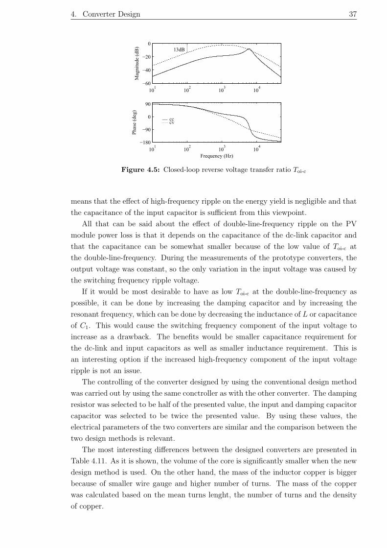
4. Converter Design 37
101
102
103
104
−60
−40
−20
0
Mag
nit
ude
(dB
)
101
102
103
104
−180
−90
0
90
Phas
e (d
eg)
Frequency (Hz)
cccv
13dB
cccv
Figure 4.5: Closed-loop reverse voltage transfer ratio Toi-c
means that the effect of high-frequency ripple on the energy yield is negligible and that
the capacitance of the input capacitor is sufficient from this viewpoint.
All that can be said about the effect of double-line-frequency ripple on the PV
module power loss is that it depends on the capacitance of the dc-link capacitor and
that the capacitance can be somewhat smaller because of the low value of Toi-c at
the double-line-frequency. During the measurements of the prototype converters, the
output voltage was constant, so the only variation in the input voltage was caused by
the switching frequency ripple voltage.
If it would be most desirable to have as low Toi-c at the double-line-frequency as
possible, it can be done by increasing the damping capacitor and by increasing the
resonant frequency, which can be done by decreasing the inductance of L or capacitance
of C1. This would cause the switching frequency component of the input voltage to
increase as a drawback. The benefits would be smaller capacitance requirement for
the dc-link and input capacitors as well as smaller inductance requirement. This is
an interesting option if the increased high-frequency component of the input voltage
ripple is not an issue.
The controlling of the converter designed by using the conventional design method
was carried out by using the same conctroller as with the other converter. The damping
resistor was selected to be half of the presented value, the input and damping capacitor
capacitor was selected to be twice the presented value. By using these values, the
electrical parameters of the two converters are similar and the comparison between the
two design methods is relevant.
The most interesting differences between the designed converters are presented in
Table 4.11. As it is shown, the volume of the core is significantly smaller when the new
design method is used. On the other hand, the mass of the inductor copper is bigger
because of smaller wire gauge and higher number of turns. The mass of the copper
was calculated based on the mean turns lenght, the number of turns and the density
of copper.

4. Converter Design 38
If MP3210LDGC core would be used instead of the selected MP3310LDGC, the
volume of the core would be 3.52cm2 as presented in Table 4.2. In this case, the
number of turns should be 20 leading to 41 grams as a mass of the inductor copper.
Thus, the percentage decrease of the core volume would be 46%, and the percentage
decrease of the inductor copper mass 25%. Thus, it cannot be denied that the new
design method leads to cost savings. Unfortunately this core was not available from
the manufacturer, so MP3310LDGC had to be used in the prototype converter.
Table 4.11: Summary of the main differences between the converter prototypes.
CM NM Decrease in %
Volume of the core (cm2) 5.34 1.89 65Mass of the inductor copper (g) 29 31 -8.4Thermal resistance of the heat sink (K/W) 6.5 14.7 -126Capacitance of input capacitor (µF) 20 10 50Capacitance of damping capacitor (µF) 20 10 50Width of the PCB copper (mm) 9.6 4.8 50Current rating of the connectors (A) 23 12 47.8
As it is shown in Table 4.11, the heat sink of the MOSFET have to be much bigger
when the conventional design method is used. Also capacitance requirement is higher
as discussed earlier. The width requirement of the PCB copper was calculated by
specifying that the tolerable increase in temperature is to be 30 degrees and that the
copper thickness is 35µm. Also the connectors were selected to the converters according
the values presented in Table 4.11.

39
5. MEASUREMENTS
All measurements presented in this chapter has been made by using agilent E4360A
solar array simulator (SAS) as a source and three series connected 12V batteries in
parallel with Chroma 63103A current sink as a load. The same SAS is proved to
emulate the dynamical properties of NAPS NP190GKg PV module accurately enough
in the prior research [9]. The values of NAPS NP190GKg PV module in STC presented
in Table 2.1 was used in the SAS. The measurements were made in the CC region, at
the MPP and in the CV region with the voltage and current values of 5V/7.98A,
25.9V/7.33A and 31V/2.6A, respectively.
5.1 Prototypes
Both prototypes of the designed converters are divided into two circuit boards. The first
circuit board includes the power-stage, the driver circuit, and the measurement circuit.
The second circuit board is the DSP development platform eZdsp TMS320F28335,
which handles the controlling. The controller was implemented in the DSP by using C
programming language.
The circuit diagram of the power-stage is presented for both of the converters in
Appendix B. There are differences in the damping network, inductor and input capac-
itor as discussed earlier. Also the circuit diagram of the measurement circuit for the
input voltage is presented, which is basically a differential amplifier with a low-pass
filter. The purpose of this circuit is to scale the input voltage to a level acceptable for
the AD converter and to remove high-frequency disturbances. The last circuit diagram
in Appendix B includes the driver circuit and the voltage regulator of the measurement
circuit.
The control signal of the PWM output of the DSP is connected to the input of
the driver circuit and the output of the measurement circuit is connected to the AD
converter of the DSP. The supply voltage of 10V for the driver is provided from the
laboratory power supply.
Photograph of the converter prototypes is presented in Fig. 5.1. The upper con-
verter is Converter CM and the lower is Converter NM. As it is clearly visible, the
inductor, connectors and the heat sink of the MOSFET are heavier when the conven-
tional design method is used. It should be noted that only the other of the two similar
inductors is visible in Fig. 5.1, the other one is under the PCB.

5. Measurements 40
a)
b)
Inductor
Inductor
Diode
Diode
MOSFET
MOSFET
Figure 5.1: Prototypes: a) Converter CM, and b) Converter NM.
As the difference in the size of these two converters is remarkable, it is clear that
the second design method might be desirable in the applications, where the cost and
size are determining factors in design.
5.2 Thermal Distribution
Temperature distribution of the converters was measured at three operating points
by using NEC TH7800 Thermo Tracer. It was first waited that the converter under
measurement reached its final temperature before the thermal image was taken. The
thermal distribution of the prototype converters is presented in Fig. 5.2 when they
operate at the MPP in the STC. The upper image corresponds to Converter CM and
the lower image corresponds to Converter NM.
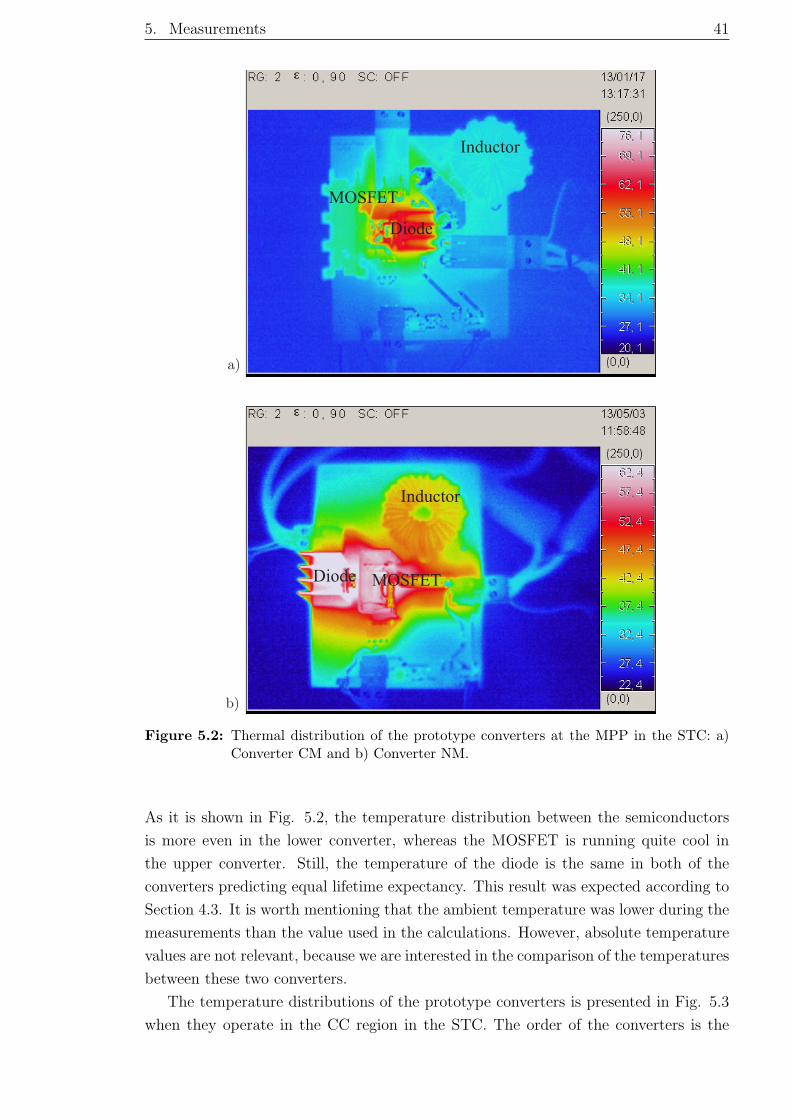
5. Measurements 41
Inductor
MOSFET
Diode
Inductor
Diode MOSFET
a)
b)
Figure 5.2: Thermal distribution of the prototype converters at the MPP in the STC: a)Converter CM and b) Converter NM.
As it is shown in Fig. 5.2, the temperature distribution between the semiconductors
is more even in the lower converter, whereas the MOSFET is running quite cool in
the upper converter. Still, the temperature of the diode is the same in both of the
converters predicting equal lifetime expectancy. This result was expected according to
Section 4.3. It is worth mentioning that the ambient temperature was lower during the
measurements than the value used in the calculations. However, absolute temperature
values are not relevant, because we are interested in the comparison of the temperatures
between these two converters.
The temperature distributions of the prototype converters is presented in Fig. 5.3
when they operate in the CC region in the STC. The order of the converters is the

5. Measurements 42
same as in Fig. 5.2.
Inductor
Inductor
Diode
MOSFET
MOSFETDiode
a)
b)
Figure 5.3: Thermal distribution of the prototype converters in the CC region in the STC:a) Converter CM and b) Converter NM.
As it is shown in Fig. 5.3, the temperature distribution between the semiconductors
is more even in the upper converter. This was expected, because the semiconductor
power losses of the upper converter were calculated at this operating point and the
calculated values were used in the heat sink selection. The temperature distribution of
the lower converter is more uneven, but the most important thing is that the temper-
ature of the MOSFET is not higher than the temperature of the diode at the MPP.
This implies that the MOSFET is not overheated in the lower converter even if its
temperature is higher than in the upper converter.
As it is visible in Figs. 5.2 and 5.3, the maximum power loss of the MOSFET occurs

5. Measurements 43
at the minimum input voltage, and the maximum power loss of the diode occurs at the
MPP. This verifies the results that were presented in Section 4.3. The thermal image of
the prototype converters was also taken in the CV region in the STC and is presented
in Fig. 5.4. The order of the converters is the same as in Fig. 5.2.
Inductor
Inductor
MOSFET
MOSFET
Diode
Diode
a)
b)
Figure 5.4: Thermal distribution of the prototype converters in the CV region in the STC:a) Converter CM and b) Converter NM.
As it is shown in Fig. 5.4, the temperature levels in both of the converters are low,
which is caused by the low output power and current of the PV module in the CV region.
This is also consistent with the discussion in Section 4.3. The overload protection of
the converter connected to PV module can be made my moving the operating point
away from the MPP. According to Fig. 5.3 and Fig. 5.4, the operating point should
be moved towards the CV region instead of the CC region for more efficient cooling.

5. Measurements 44
As a summary, it can be said that the converter, which is designed by using the
conventional design method, is oversized, because the MOSFET and inductor are run-
ning cool, whereas in the converter, which is designed by using the new design method
the MOSFET is as hot as the diode.
5.3 Input Voltage Ripple
The input voltage ripple of the converters was measured at the MPP in the STC by
using LeCroy104MXi oscilloscope. The measured input voltages are presented in Figs.
5.5 and 5.6. As it is shown, the amplitude of the ripple component at the input voltage
is approximately equal, which verifies that the converters operate similarly from this
point of view and thus, the comparison is reasonable. The peak-to-peak value of the
voltage ripple is approximately 250mV. This value was used when the effect of the
voltage ripple on power output of the PV module was calculated in Section 4.5.
2μs
in (100mV/div)u
Figure 5.5: The input voltage ripple of Converter CM.
in (100mV/div)u
2μs
Figure 5.6: The input voltage ripple of Converter NM.
5.4 Frequency Response Measurements
The frequency responses of the converter prototypes were measured by using the fre-
quency response analyzer Model 3120 of Venable Instruments. Every open-loop and
closed-loop transfer functions were measured at three operating points in order to ver-
ify the converter model and the control design. Also the impedance of the ceramic

5. Measurements 45
capacitor was measured to determine its ESR and capacitance values for the model at
these operating points. The output impedance of the SAS was also measured and its
effect on the model was taken into account. The final tuning of the model parameters
was made so that all of the predicted and measured transfer functions matched as well
as possible.
As it is shown in Figs. 5.7 and 5.8, the control to input transfer function of the
converters are quite similar with phase starting from 180 degrees and gain from 30
decibels. The resonance peak is smooth in the CC region because of the added damping
circuit as explained in Section 4.5. The predicted transfer functions (dots) correlate
well with the measurements in the CC region (solid) and in the CV region (dotted).
101
102
103
104
−20
0
20
40
60
Mag
nit
ude
(dB
)
101
102
103
104
−180
−90
0
90
180
Phas
e (d
eg)
Frequency (Hz)
predicted
cccvpredicted
cccv
Figure 5.7: Control to input transfer function of Converter CM.
101
102
103
104
−20
0
20
40
60
Mag
nit
ude
(dB
)
101
102
103
104
−180
−90
0
90
180
Phas
e (d
eg)
Frequency (Hz)
cccvpredictedpredicted
cccv
Figure 5.8: Control to input transfer function of Converter NM.
The input-voltage loop gain Lin can be solved from (3.9) by taking into account that
the sensing gain is set to unity in the program of the DSP. Thus, Lin can be calculated
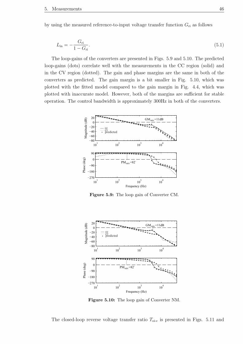
5. Measurements 46
by using the measured reference-to-input voltage transfer function Gri as follows
Lin = −Gri
1−Gri
. (5.1)
The loop-gains of the converters are presented in Figs. 5.9 and 5.10. The predicted
loop-gains (dots) correlate well with the measurements in the CC region (solid) and
in the CV region (dotted). The gain and phase margins are the same in both of the
converters as predicted. The gain margin is a bit smaller in Fig. 5.10, which was
plotted with the fitted model compared to the gain margin in Fig. 4.4, which was
plotted with inaccurate model. However, both of the margins are sufficient for stable
operation. The control bandwidth is approximately 300Hz in both of the converters.
101
102
103
104
−80
−60
−40
−20
0
20
Mag
nit
ud
e (d
B)
101
102
103
104
−270
−180
−90
0
90
Ph
ase
(deg
)
Frequency (Hz)
predicted
cccv
MINGM =11dB
MINPM =82o
predicted
cccv
Figure 5.9: The loop gain of Converter CM.
101
102
103
104
−80
−60
−40
−20
0
20
Mag
nit
ude
(dB
)
101
102
103
104
−270
−180
−90
0
90
Phas
e (d
eg)
Frequency (Hz)
predicted
cccv
MINGM =11dB
MINPM =82o
predicted
cccv
Figure 5.10: The loop gain of Converter NM.
The closed-loop reverse voltage transfer ratio Toi-c is presented in Figs. 5.11 and

5. Measurements 47
5.12. The predicted transfer functions (dots) correlate well with the measurements in
the CC region (solid) and in the CV region (dotted). As it is shown, the magnitude at
100Hz is -13dB in both of the converters in the CC region, which verifies the similarity
of the attenuation behavior of the converters. It is also visible that the magnitude
of Toi-c is usually lower than -13dB at 100Hz, because the operation point is varying
between the lowest and highest input voltage. The attenuation is most important in
the MPP, because the ripple at the PV module voltage would cause highest losses.
According to the input-voltage ripple and frequency response measurements, it can
be said that both of the converters operate electrically similarly in terms of the given
quantities. Because Converter NM offers the same performance as Converter CM with
a lower inductor core size and smaller capacitors, converter NM is more optimal. Thus,
the measurements verify the claims that are presented earlier in this thesis.
101
102
103
104
−60
−40
−20
0
Mag
nit
ude
(dB
)
101
102
103
104
−180
−90
0
90
Phas
e (d
eg)
Frequency (Hz)
predicted
cccv
13dB
predicted
cccv
Figure 5.11: Closed-loop reverse voltage transfer ratio Toi-c of Converter CM.
101
102
103
104
−60
−40
−20
0
Mag
nit
ud
e (d
B)
101
102
103
104
−180
−90
0
90
Ph
ase
(deg
)
Frequency (Hz)
cccvpredicted
13dB
predicted
cccv
Figure 5.12: Closed-loop reverse voltage transfer ratio Toi-c of Converter NM.

48
6. CONCLUSIONS
Two differently designed boost-power-stage converters were implemented and compared
to each other in this thesis. The first converter was designed by using the conventional
method and the second converter was designed by using the new method taking into
account the maximum values of the PV module output.
In the conventional design method, it was assumed that the maximum power loss
of the diode and power switch would occur in the minimum input voltage condition.
However, it was theoretically explained and verified by the measurements that the max-
imum power loss of the power switch occurs in the minimum input voltage condition,
whereas the maximum power loss of the diode occurs when the PV module is at the
maximum power point.
The converters were designed in such a way that both have the same amount of
switching frequency input-voltage ripple and equal ability to prevent low frequency
output voltage ripple from affecting the input voltage. Despite of this electrical simi-
larity, which was also verified by the measurements, the converter that was designed by
using the second design method has smaller core size, less capacitance in the input and
damping capacitors as well as has smaller heat sink of MOSFET. Thus, it is possible
to obtain significant cost savings if the second design method is used.
In the new design method, it was taken into account that the output power of the
PV module is momentarily high due to peaks in solar irradiance. This way it can
be ensured that the inductor will not saturate in any circumstances. If the inductor
saturation and semiconductor overheating can be prevented by some kind of protection
method, it would be possible to undersize the components and the difference between
the presented design methods would be even more significant. However, this requires
more research on different protection methods and thus might be a possible topic in
the future.
The results presented in this thesis are most valuable for a manufacturer, who
delivers both the PV generator and the power electronic devices, because the properties
of a PV generator are known when the converter or inverter is designed. On the other
hand, it might be interesting for a manufacturer, who produces only PV inverters to
know how much oversizing the conventional sizing method causes. Even if the converter
prototypes were designed for a PVG consisting only one PV module, the results are
applicable also for a string of modules. Only the voltages are scaled but the current
remains the same.

49
REFERENCES
[1] B. K. Bose, “Global warming: energy, environmental pollution, and the impact of
power electronics,” IEEE Industrial Electronics Magazine, pp. 6–17, March 2010,
dOI: 10.1109/MIE.2010.935860.
[2] “Global market outlook for pv until 2016,” [Cited 13/5/2013]. [Online]. Available:
http://www.epia.org/
[3] C. Ho, H. Breuninger, S. Pettersson, G. Escobar, L. Serpa, and A. Coccia, “Prac-
tical design and implementation procedure of an interleaved boost converter using
sic diodes for pv applications,” IEEE Transactions on Power Electronics, vol. 27,
no. 6, pp. 2835–2845, June 2012.
[4] S. Mattila, “Kolmitasoisen nostavan hakkuriteholahteen kuristimen suunnittelu ja
optimointi,” Master’s thesis, Tampere University of Technology, 2009, tampere.
[5] “Danfoss dlx ul inverter series datasheet,” [Cited 13/5/2013].
[Online]. Available: http://www.danfoss.com/NR/rdonlyres/
91638FD3-9A30-410A-9C2D-404B62FE75B4/0/Danfoss DLX DataSheet lowres.
[6] “Vacon 8000 solar inverter series datasheet,” [Cited 13/5/2013].
[Online]. Available: http://www.vacon.com/ImageVaultFiles/id 3122/cf 2/
Vacon-8000-Solar-Brochure-BC00414F-EN.PDF?634852861613100000
[7] “Siemens sinvert solar inverter series datasheet,” [Cited 13/5/2013]. [Online].
Available: http://www.automation.siemens.com/mcms/solar-inverter/en/pvm/
Pages/Default.aspx?tabcardname=Technical20Features
[8] M. Villalva, J. Gazoli, and E. Ruppert, “Comprehensive approach to modeling
and simulation of photovoltaic arrays,” IEEE Transactions on Power Electronics,
vol. 24, no. 5, pp. 1198–1208, May 2009.
[9] J. Puukko, A. Maki, T. Messo, J. Huusari, J. Jokipii, J. Viinamaki, D. Lobera,
S. Valkealahti, and T. Suntio, “Photovoltaic generator as an input source for power
electronic converters,” IEEE Transactions on Power Electronics, vol. 28, no. 6, pp.
3028–3038, June 2013.
[10] C. Sullivan, J. Awerbuch, and A. Latham, “Decrease in photovoltaic power output
from ripple: Simple general calculation and the effect of partial shading,” IEEE
Transactions on Power Electronics, vol. 28, no. 2, pp. 740–747, February 2013.
[11] C. Balafas, M. Athanassopoulou, T. Argyropoulos, P.Skafidas, and C.T.Dervos,
“Effect of the diffuse solar radiation on photovoltaic inverter output,”MELECON
2010 - 2010 15th IEEE Mediterranean Electrotechnical Conference, pp. 58–63,
2010.
REFERENCES 50
[12] A. Maki and S. Valkealahti, “Power losses in long string and parallel-connected
short strings of series-connected silicon-based photovoltaic modules due to partial
shading conditions,” IEEE Transactions on Energy Conversion, vol. 27, no. 1, pp.
173–183, March 2012.
[13] E. Haberlin, Photovoltaics: System Design and Practice. Wiley, 2012, iSBN:
978-1-119-99285-1.
[14] J. Luoma, J. Kleissl, and K. Murray, “Optimal inverter sizing considering cloud
enhancement,” Solar energy, vol. 86, no. 1, pp. 421–429, January 2012.
[15] W. Xiao, N. Ozog, and W. Dunford, “Topology study of photovoltaic interface for
maximum power point tracking,” IEEE Transactions on Industrial Electronics,
vol. 54, no. 3, pp. 1696–1704, June 2007.
[16] T. Messo, J. Puukko, and T. Suntio, “Effect of mpp-tracking dc/dc converter on
vsi-based photovoltaic inverter dynamics,” 6th IET International Conference on
Power Electronics, Machines and Drives (PEMD 2012), pp. 1–6, 2012.
[17] J. Wyatt and L. Chua, “Nonlinear resistive maximum power theorem, with solar
cell application,” IEEE Transactions on Circuits and Systems, vol. 30, no. 11, pp.
824–828, November 1983.
[18] J. Leppaaho, L. Nousiainen, J. Puukko, J. Huusari, and T. Suntio, “Implementing
current-fed converters by adding an input capacitor at the input of voltage-fed
converter for interfacing solar generator,” 14th Int. Power Electronics and Motion
Control Conf. (EPE/PEMC), pp. T12–81–T12–88, 2010.
[19] R. Erickson and D. Maksimovic, Fundamentals of Power Electronics. Springer
Science+Business Media, 2004, iSBN: 978-0-7923-7270-7.
[20] T. Messo, J. Jokipii, and T. Suntio,“Steady-state and dynamic properties of boost-
power-stage converter in photovoltaic applications,” 3rd IEEE International Sym-
posium on Power Electronics for Distributed Generation Systems (PEDG 2012),
pp. 34–40, 2012.
[21] H. Hu, S. Harb, N. Kutkut, I. Batarseh, and Z. J. Shen, “Power decoupling tech-
niques for micro-inverters in pv systems-a review,” Energy Conversion Congress
and Exposition (ECCE), pp. 3235–3240, 2010.
[22] S. Chen, P. Li, D. Brady, and B. Lehman, “Optimal inverter sizing considering
cloud enhancement,” Solar energy, vol. 87, no. 1, pp. 96–116, January 2013.
[23] J. Mondol, Y. Yohanis, and B. Norton, “Optimal sizing of array and inverter for
grid-connected photovoltaic systems,”Solar energy, vol. 80, no. 12, pp. 1517–1539,
December 2006.

REFERENCES 51
[24] “Power factor correction inductor design for switched mode power supplies using
metglas powerlite c-cores - application guide,” [Cited 20/10/2012]. [Online].
Available: http://www.metglas.com/downloads/apps/pfc.pdf
[25] “Metglass microlite technical datasheet,” [Cited 13/5/2013]. [On-
line]. Available: http://www.hitachimetals.com/product/amorphous/
microliteinductorcores/documents/Micorlite technical bulletin opt.pdf
[26] A. V. Bossche and V. C. Valchev, Inductors and Transformers for Power Elec-
tronics. Taylor & Francis, 2005, iSBN: 978-1-57444-679-1.
[27] N. Mohan, T. Undeland, and W. Robbins, Power Electronics. John Wiley &
Sons, Inc, 2003, iSBN: 0-471-42908-2.
[28] “Mosfet power losses calculation using the datasheet
parameters - infineon application note,” [Cited
13/5/2013]. [Online]. Available: http://www.scribd.com/doc/34308439/
MOSFET-Power-Losses-Calculation-Using-the-Data-Sheet-Parameters
[29] “Calculation of reverse losses in a power diode - st
microelectronics application note,” [Cited 13/5/2013]. [Online].
Available: http://www.st.com/st-web-ui/static/active/jp/resource/technical/
document/application note/DM00044087.pdf
[30] “Magnetics designer user manual,” [Cited 13/5/2013]. [Online]. Available: http://
www.intusoft.com/lit/Magdes.pdf
[31] “Venable technical paper #4 minimizing input filter requirements in military
power supply design,” [Cited 13/5/2013]. [Online]. Available: http://www.
venable.biz/tp-04.pdf

52
A. IMPEDANCE MEASUREMENT OF THE
INDUCTORS
Frequency response analyzer Amplifier
Injection trasformer
12VBattery
Chroma in CCH mode
CL
LuLi
Ch1 Ch2INJ out INOUT
Figure A.1: Inductor impedance measurement setup.
101
102
103
104
−40
−20
0
20
Mag
nit
ude
(dB
)
101
102
103
104
0
45
90
Phas
e (d
eg)
Frequency (Hz)
2.6A7.33A23Afitted curve
Figure A.2: Measured impedances of the 43-µH inductor for different bias currents withfitted curves.

A. Impedance Measurement of The Inductors 53
101
102
103
104
−40
−20
0
20
40
Mag
nit
ude
(dB
)
101
102
103
104
0
45
90
Phas
e (d
eg)
Frequency (Hz)
2.6A7.33A11Afitted curve
Figure A.3: Measured impedances of the 89-µH inductor for different bias currents withfitted curves.
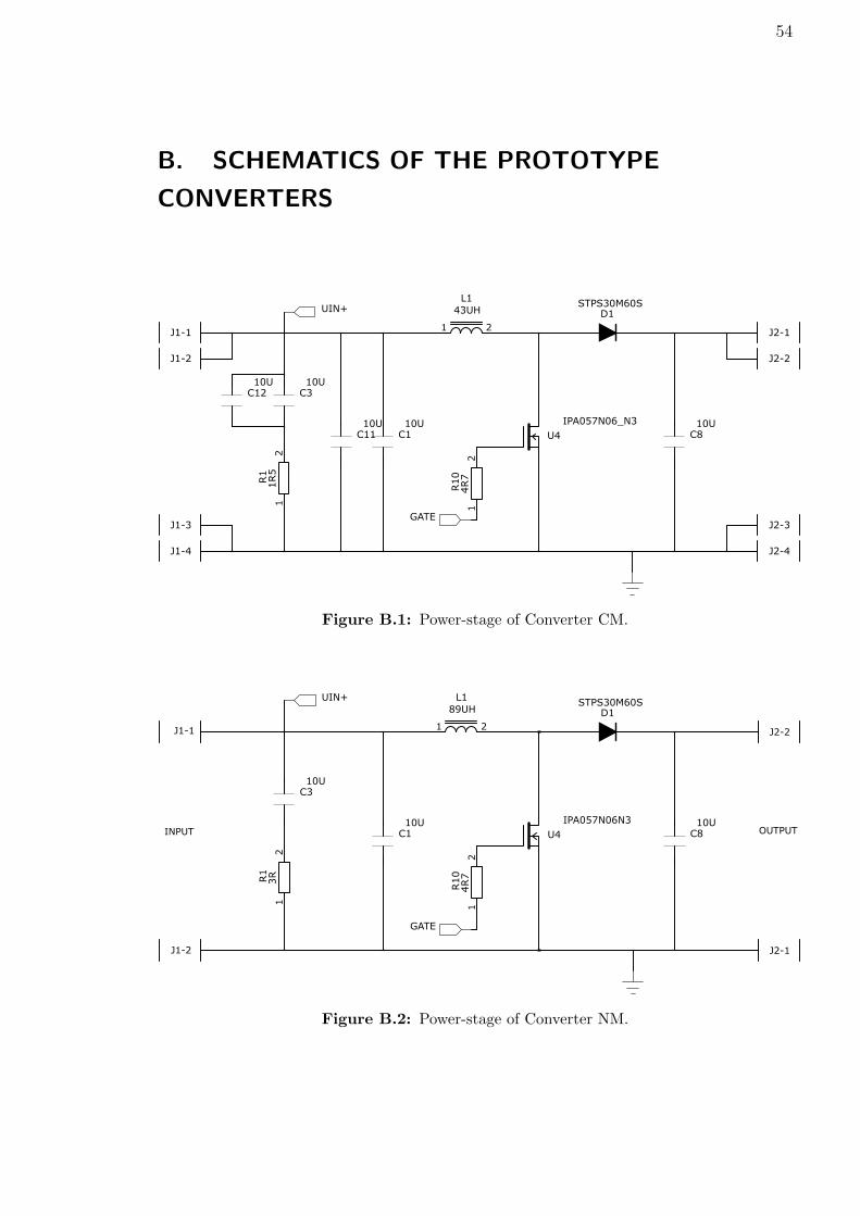
54
B. SCHEMATICS OF THE PROTOTYPE
CONVERTERS
C1
10U
12
R1
1R5
12
R10
4R7
C3
10U
C8
10U
D1STPS30M60S
1 2
L1
43UH
C11
10U
U4
IPA057N06_N3
J1-1
J1-2
J1-3
J1-4
J2-1
J2-2
J2-3
J2-4
C12
10U
UIN+
GATE
Figure B.1: Power-stage of Converter CM.
INPUT OUTPUT
J1-1
J1-2 J2-1
J2-2
C1
10U
12
R1
3R
1 2
L1
89UH
U4
IPA057N06N3
12
R10
4R7
C3
10U
C8
10U
D1STPS30M60S
UIN+
GATE
Figure B.2: Power-stage of Converter NM.
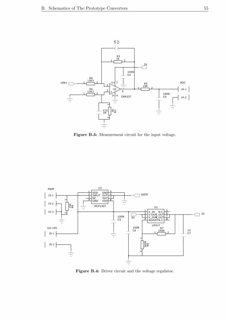
B. Schematics of The Prototype Converters 55
ADC
J4-1
J4-2
-
+
2
3
4V-
6
7V+
U2
OPA337
1 2
R510R
C9
100N
1 2
R31K
1 2
R613K3
12
R2
1K
C2
1N
C101N
1 2
R413K3
C4
100N
3V
UIN+
Figure B.3: Measurement circuit for the input voltage.
PWM
Uin 10V
J3-1
J3-2
J3-3
1VDD
2INPUT
3NC
4GND
5GND
6OUT
7OUT
8VDD
U3
MCP1407
1V_IN
2V-OUT
3V_OUT
4ADJUST
5N.C.
6V_OUT
7V_OUT
8N.C.
U1
LM317
C5
100N
C6
100N
C7
1U1 2
R7240R
12
R8
360R
12
R9
10K
J5-1
J5-2
3V
3V
GATE
Figure B.4: Driver circuit and the voltage regulator.