Analysis and Implementation of Buck Boost Voltage Source ... · Analysis and Implementation of Buck...
7
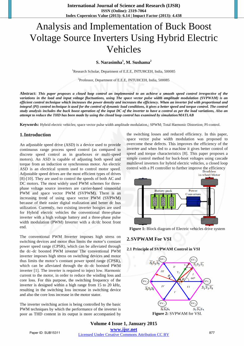
International Journal of Science and Research (IJSR) ISSN (Online): 2319-7064 Index Copernicus Value (2013): 6.14 | Impact Factor (2013): 4.438 Volume 4 Issue 1, January 2015 www.ijsr.net Licensed Under Creative Commons Attribution CC BY Analysis and Implementation of Buck Boost Voltage Source Inverters Using Hybrid Electric Vehicles S. Narasimha 1 , M. Sushama 2 1 Research Scholar, Department of E.E.E, JNTUHCEH, India, 500085 2 Professor, Department of E.E.E, JNTUHCEH, India, 500085 Abstract: This paper proposes a closed loop control an implemented to an achieve a smooth speed control irrespective of the variations in the load and input voltage fluctuations, using The space vector pulse width amplitude modulation (SVPWAM) is an efficient control technique which increases the power density and increases the efficiency. When an inverter fed with proportional and integral (PI) control technique is used for the control of dynamic load conditions, it gives a better speed and torque control. The control study analysis includes the buck boost operation of the input DC of the inverter to have a control as per the load variations, Also an attempt to reduce the THD has been made by using the closed loop control has examined by simulation/MATLAB Keywords: Hybrid electric vehicles; space vector pulse width amplitude modulation,; SPWM; Total Harmonic Distortion; PI-control. 1. Introduction An adjustable speed drive (ASD) is a device used to provide continuous range process speed control (as compared to discrete speed control as in gearboxes or multi-speed motors). An ASD is capable of adjusting both speed and torque from an induction or synchronous motor. An electric ASD is an electrical system used to control motor speed. Adjustable speed drives are the most efficient types of drives [8]-[10]. They are used to control the speeds of both AC and DC motors. The most widely used PWM schemes for three- phase voltage source inverters are carrier-based sinusoidal PWM and space vector PWM (SVPWM). There is an increasing trend of using space vector PWM (SVPWM) because of their easier digital realization and better dc bus utilization. Currently, two existing inverter boogies are used for Hybrid electric vehicles the conventional three-phase inverter with a high voltage battery and a three-phase pulse width modulation (PWM) Inverter with a dc/dc boost front end. The conventional PWM Inverter imposes high stress on switching devices and motor thus limits the motor’s constant power speed range (CPSR), which can be alleviated through the dc–dc boosted PWM inverter The conventional PWM inverter imposes high stress on switching devices and motor thus limits the motor’s constant power speed range (CPSR), which can be alleviated through the dc–dc boosted PWM inverter [1]. The inverter is required to inject low. Harmonic current to the motor, in order to reduce the winding loss and core loss. For this purpose, the switching frequency of the inverter is designed within a high range from 15 to 20 kHz, resulting in the switching loss increase in switching device and also the core loss increase in the motor stator. The inverter switching action is being controlled by the basic PWM techniques by which the performance of the inverter is poor as THD content in its output is more accompanied by the switching losses and reduced efficiency. In this paper, space vector pulse width modulation was proposed to overcome these defects. This improves the efficiency of the inverter and when fed to a machine it gives better control of speed and torque characteristics [8]. This paper proposes a simple control method for buck-boot voltages using cascade multilevel inverters for hybrid electric vehicles, a closed loop control with a PI controller to further improve the efficiency Figure 1: Block diagram of Electric vehicles drive system 2. SVPWAM For VSI 2.1 Principle of SVPWAM Control in VSI Figure 2: SVPWAM for VSI. Paper ID: SUB15311 877
Transcript of Analysis and Implementation of Buck Boost Voltage Source ... · Analysis and Implementation of Buck...
International Journal of Science and Research (IJSR) ISSN (Online): 2319-7064
Index Copernicus Value (2013): 6.14 | Impact Factor (2013): 4.438
Volume 4 Issue 1, January 2015 www.ijsr.net
Licensed Under Creative Commons Attribution CC BY
Analysis and Implementation of Buck Boost Voltage Source Inverters Using Hybrid Electric
Vehicles
S. Narasimha1, M. Sushama2
1Research Scholar, Department of E.E.E, JNTUHCEH, India, 500085
2Professor, Department of E.E.E, JNTUHCEH, India, 500085 Abstract: This paper proposes a closed loop control an implemented to an achieve a smooth speed control irrespective of the variations in the load and input voltage fluctuations, using The space vector pulse width amplitude modulation (SVPWAM) is an efficient control technique which increases the power density and increases the efficiency. When an inverter fed with proportional and integral (PI) control technique is used for the control of dynamic load conditions, it gives a better speed and torque control. The control study analysis includes the buck boost operation of the input DC of the inverter to have a control as per the load variations, Also an attempt to reduce the THD has been made by using the closed loop control has examined by simulation/MATLAB Keywords: Hybrid electric vehicles; space vector pulse width amplitude modulation,; SPWM; Total Harmonic Distortion; PI-control. 1. Introduction
An adjustable speed drive (ASD) is a device used to provide continuous range process speed control (as compared to discrete speed control as in gearboxes or multi-speed motors). An ASD is capable of adjusting both speed and torque from an induction or synchronous motor. An electric ASD is an electrical system used to control motor speed. Adjustable speed drives are the most efficient types of drives [8]-[10]. They are used to control the speeds of both AC and DC motors. The most widely used PWM schemes for three-phase voltage source inverters are carrier-based sinusoidal PWM and space vector PWM (SVPWM). There is an increasing trend of using space vector PWM (SVPWM) because of their easier digital realization and better dc bus utilization. Currently, two existing inverter boogies are used for Hybrid electric vehicles the conventional three-phase inverter with a high voltage battery and a three-phase pulse width modulation (PWM) Inverter with a dc/dc boost front end. The conventional PWM Inverter imposes high stress on switching devices and motor thus limits the motor’s constant power speed range (CPSR), which can be alleviated through the dc–dc boosted PWM inverter The conventional PWM inverter imposes high stress on switching devices and motor thus limits the motor’s constant power speed range (CPSR), which can be alleviated through the dc–dc boosted PWM inverter [1]. The inverter is required to inject low. Harmonic current to the motor, in order to reduce the winding loss and core loss. For this purpose, the switching frequency of the inverter is designed within a high range from 15 to 20 kHz, resulting in the switching loss increase in switching device and also the core loss increase in the motor stator. The inverter switching action is being controlled by the basic PWM techniques by which the performance of the inverter is poor as THD content in its output is more accompanied by
the switching losses and reduced efficiency. In this paper, space vector pulse width modulation was proposed to overcome these defects. This improves the efficiency of the inverter and when fed to a machine it gives better control of speed and torque characteristics [8]. This paper proposes a simple control method for buck-boot voltages using cascade multilevel inverters for hybrid electric vehicles, a closed loop control with a PI controller to further improve the efficiency
Figure 1: Block diagram of Electric vehicles drive system
2. SVPWAM For VSI 2.1 Principle of SVPWAM Control in VSI
Figure 2: SVPWAM for VSI.
Paper ID: SUB15311 877
International Journal of Science and Research (IJSR) ISSN (Online): 2319-7064
Index Copernicus Value (2013): 6.14 | Impact Factor (2013): 4.438
Volume 4 Issue 1, January 2015 www.ijsr.net
Licensed Under Creative Commons Attribution CC BY
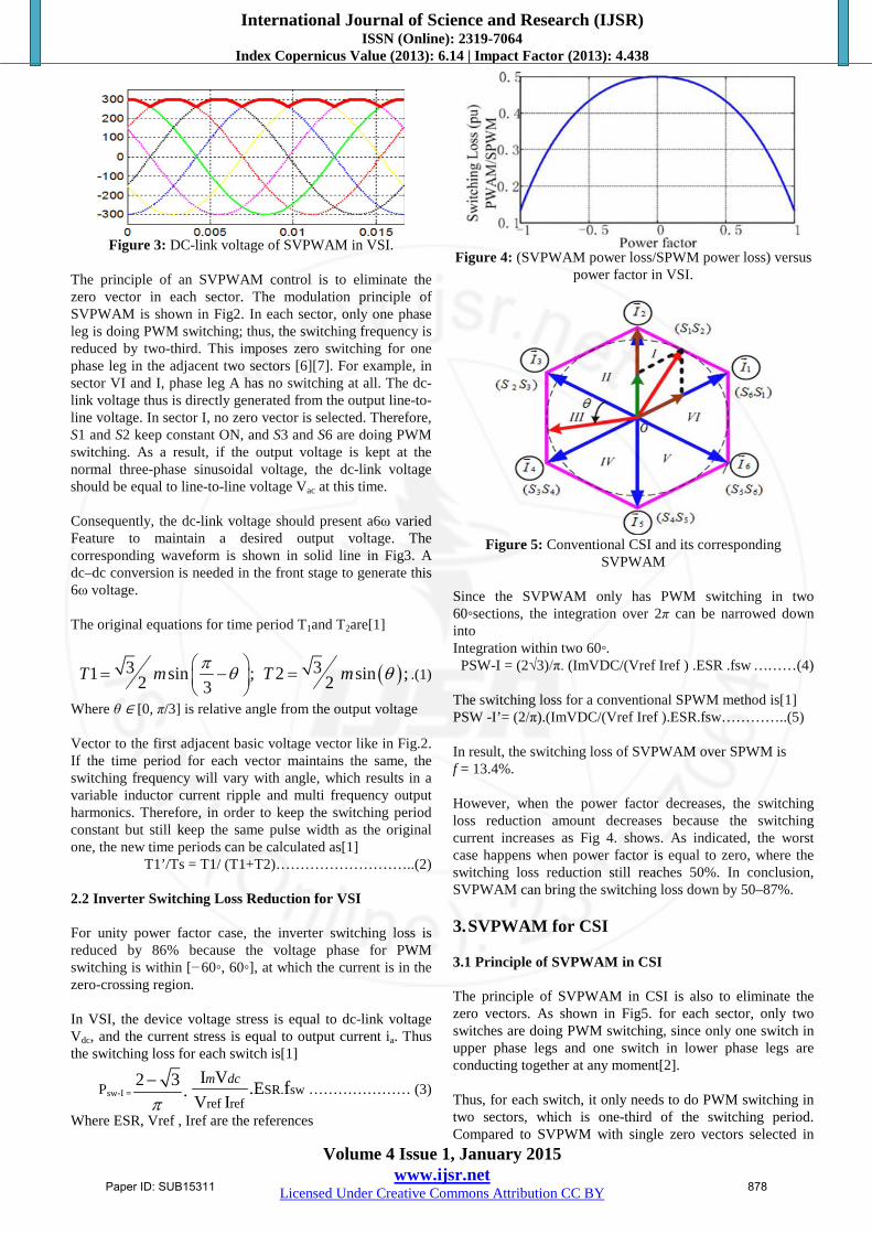
Figure 3: DC-link voltage of SVPWAM in VSI.
The principle of an SVPWAM control is to eliminate the zero vector in each sector. The modulation principle of SVPWAM is shown in Fig2. In each sector, only one phase leg is doing PWM switching; thus, the switching frequency is reduced by two-third. This imposes zero switching for one phase leg in the adjacent two sectors [6][7]. For example, in sector VI and I, phase leg A has no switching at all. The dc-link voltage thus is directly generated from the output line-to-line voltage. In sector I, no zero vector is selected. Therefore, S1 and S2 keep constant ON, and S3 and S6 are doing PWM switching. As a result, if the output voltage is kept at the normal three-phase sinusoidal voltage, the dc-link voltage should be equal to line-to-line voltage Vac at this time. Consequently, the dc-link voltage should present a6ω varied Feature to maintain a desired output voltage. The corresponding waveform is shown in solid line in Fig3. A dc–dc conversion is needed in the front stage to generate this 6ω voltage. The original equations for time period T1and T2are[1]
31 sin ;2 3T m π θ = −
( )32 sin ;2T m θ= .(1)
Where θ ∈ [0, π/3] is relative angle from the output voltage Vector to the first adjacent basic voltage vector like in Fig.2. If the time period for each vector maintains the same, the switching frequency will vary with angle, which results in a variable inductor current ripple and multi frequency output harmonics. Therefore, in order to keep the switching period constant but still keep the same pulse width as the original one, the new time periods can be calculated as[1]
T1’/Ts = T1/ (T1+T2)………………………..(2) 2.2 Inverter Switching Loss Reduction for VSI For unity power factor case, the inverter switching loss is reduced by 86% because the voltage phase for PWM switching is within [−60◦, 60◦], at which the current is in the zero-crossing region. In VSI, the device voltage stress is equal to dc-link voltage Vdc, and the current stress is equal to output current ia. Thus the switching loss for each switch is[1]
Psw-I =2 3 .π−
SR. swref ref
I V .EV I
fm dc………………… (3)
Where ESR, Vref , Iref are the references
Figure 4: (SVPWAM power loss/SPWM power loss) versus
power factor in VSI.
Figure 5: Conventional CSI and its corresponding
SVPWAM
Since the SVPWAM only has PWM switching in two 60◦sections, the integration over 2π can be narrowed down into Integration within two 60◦.
PSW-I = (2√3)/π. (ImVDC/(Vref Iref ) .ESR .fsw ………(4) The switching loss for a conventional SPWM method is[1] PSW -I’= (2/π).(ImVDC/(Vref Iref ).ESR.fsw…………..(5) In result, the switching loss of SVPWAM over SPWM is f = 13.4%. However, when the power factor decreases, the switching loss reduction amount decreases because the switching current increases as Fig 4. shows. As indicated, the worst case happens when power factor is equal to zero, where the switching loss reduction still reaches 50%. In conclusion, SVPWAM can bring the switching loss down by 50–87%. 3. SVPWAM for CSI 3.1 Principle of SVPWAM in CSI The principle of SVPWAM in CSI is also to eliminate the zero vectors. As shown in Fig5. for each sector, only two switches are doing PWM switching, since only one switch in upper phase legs and one switch in lower phase legs are conducting together at any moment[2]. Thus, for each switch, it only needs to do PWM switching in two sectors, which is one-third of the switching period. Compared to SVPWM with single zero vectors selected in
Paper ID: SUB15311 878

International Journal of Science and Research (IJSR) ISSN (Online): 2319-7064
Index Copernicus Value (2013): 6.14 | Impact Factor (2013): 4.438
Volume 4 Issue 1, January 2015 www.ijsr.net
Licensed Under Creative Commons Attribution CC BY
each sector, this method brings down the switching frequency by one-third.
Figure 6: Switching voltage and current when pf = 1.
Similarly, the dc-link current in this case is a 6ω varied current. It is the maximum envelope of six output currents: Ia, Ib, Ic ,−Ia ,−Ib ,−Ic , as shown in Fig 6. For example, in sector I, S1 always keeps ON, so the dc-link current is equal to Ia . The difference between dc-link current in CSI and dc-link voltage in VSI is dc-link current in CSI is overlapped with the phase current, but dc-link voltage in VSI is overlapped with the line voltage, not the phase voltage[2]. The time intervals for two adjacent vectors can be calculated in the same way as equation (1) and (2). 3.2 Inverter Switching Loss Reduction for CSI In CSI, the current stress on the switch is equal to the dc link current, and the voltage stress is equal to output line-to-line voltage, as shown the shadow area in Fig 6. Thus, the switching loss for a single switch is determined by[1] PSW -CSI =(2 −√3)/π ( idc¯ ・ V1−lpeak)/Vref Iref . ESR.fsw………………..(6)
Figure 7: (SVPWAM power loss/SPWM power loss) versus
power factor in VSI. When compared to discontinuous SVPWM, if the half switching frequency is utilized, then the switching loss of it becomes half of the result in equation (6). The corresponding switching loss ratio between SVPWAM and discontinuous SVPWM is shown in Fig 7. 4. Topologies for SVPWAM Basically, the topologies that can utilize SVPWAM have two stages: dc–dc conversion which converts a dc voltage or current into a 6ω varied dc-link voltage or current; VSI or CSI for which SVPWAM is applied[8]. One typical example
of this structure is the boost converter inverter discussed previously. However, the same function can also be implemented in a single stage, such as Z/quasi-Z/trans-Z source inverter [1].The front stage can also be integrated with inverter to form a single stage. Take current-fed quasi-Z-source inverter as an example. Instead of controlling the dc-link current Ipn to have a constant average value, the open zero state duty cycle Dop will be regulated instantaneously to control Ipm to have a 6ω fluctuate average value, resulting in a pulse type 6ω waveform at the real dc-link current Ipn, since I1 is related to the input dc current Iin by a transfer function [1] I1 =[(1 – Dop) / (1 − 2Dop)] Iin………………….(7) 5. Case Study: 1-Kw Boost-Converter Inverter
for EV Motor Drive Application 5.1 Basic Control Principle The circuit schematic and control system for a 1-kW boost converter inverter motor drive system is shown in Fig. 8. A 6ω dc-link voltage is generated from a constant dc voltage by a boost converter, using open-loop control. Inverter then could be modulated by a SVPWAM method. The specifications for t he system are input voltage is 100–200V; the average dc-linkvoltage is 300 V; output line-to-line voltage rms is 230 V; and frequency is from 60 Hz to 1 kHz.
Figure 8: SVPWAM-based boost converter-inverter motor
drive system 5.2 Voltage Constraint and Operation Region The constraint is determined by the minimum point of the 6ω Dc-link voltage. Beyond this region, conventional SPWM can be implemented. However, the dc-link voltage in this case still varies with 6ω because of the small film capacitor we selected. Thus, a modified SPWM with varying dc-link voltage will be adopted during the motor start up as shown in Fig 8. Hence, the system will achieve optimum efficiency when the motor is operating a little below or around nominal voltage. When the motor demands a low voltage during start up, efficiency is the same as the conventional SPWM-controlled inverter.
Paper ID: SUB15311 879
International Journal of Science and Research (IJSR) ISSN (Online): 2319-7064
Index Copernicus Value (2013): 6.14 | Impact Factor (2013): 4.438
Volume 4 Issue 1, January 2015 www.ijsr.net
Licensed Under Creative Commons Attribution CC BY
Figure 9: Operation region of boost-converter-inverter EV
traction drive.
Figure 10: Variable carrier SPWM control in buck mode
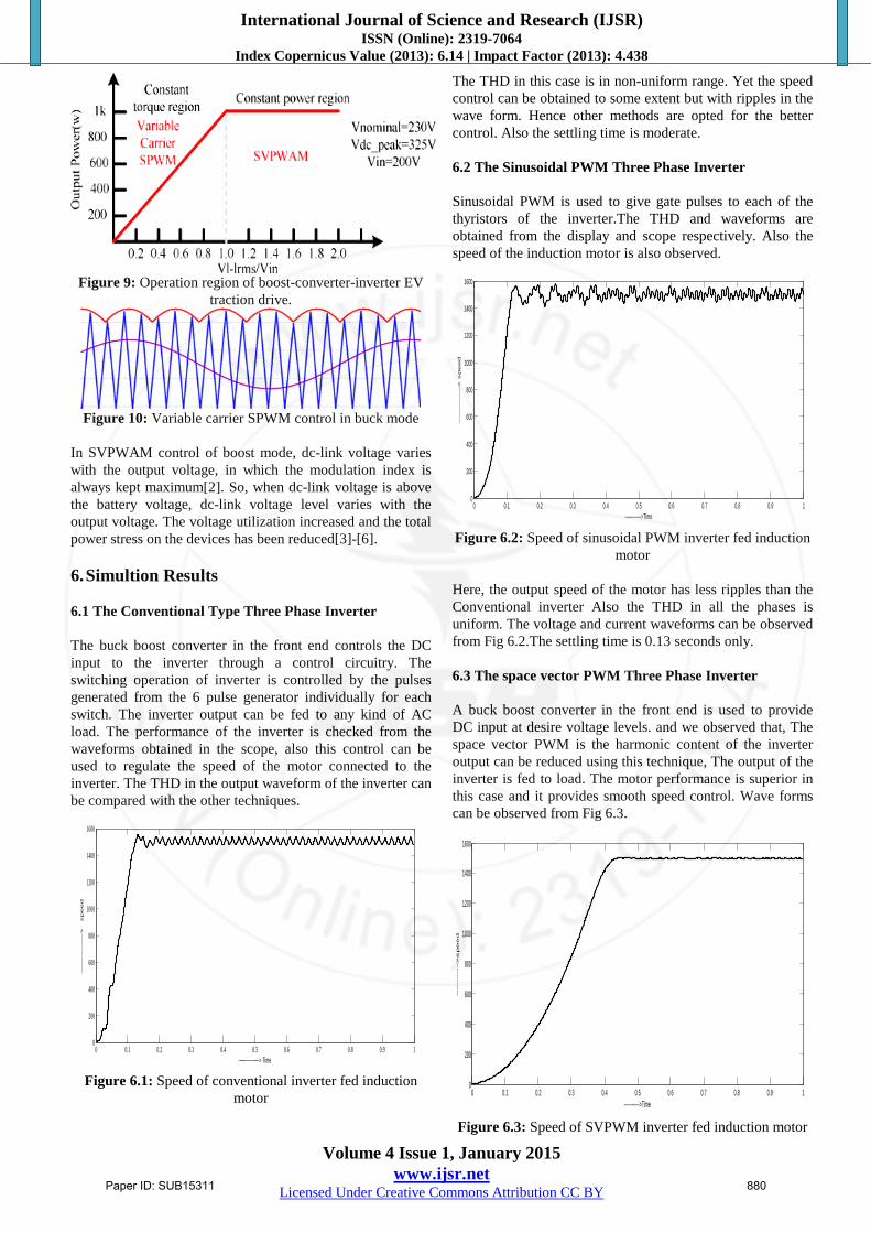
In SVPWAM control of boost mode, dc-link voltage varies with the output voltage, in which the modulation index is always kept maximum[2]. So, when dc-link voltage is above the battery voltage, dc-link voltage level varies with the output voltage. The voltage utilization increased and the total power stress on the devices has been reduced[3]-[6]. 6. Simultion Results 6.1 The Conventional Type Three Phase Inverter The buck boost converter in the front end controls the DC input to the inverter through a control circuitry. The switching operation of inverter is controlled by the pulses generated from the 6 pulse generator individually for each switch. The inverter output can be fed to any kind of AC load. The performance of the inverter is checked from the waveforms obtained in the scope, also this control can be used to regulate the speed of the motor connected to the inverter. The THD in the output waveform of the inverter can be compared with the other techniques.
0 0.1 0.2 0.3 0.4 0.5 0.6 0.7 0.8 0.9 10
200
400
600
800
1000
1200
1400
1600
-----------------> Time
----
----
----
----
>
speed
Figure 6.1: Speed of conventional inverter fed induction
motor
The THD in this case is in non-uniform range. Yet the speed control can be obtained to some extent but with ripples in the wave form. Hence other methods are opted for the better control. Also the settling time is moderate. 6.2 The Sinusoidal PWM Three Phase Inverter Sinusoidal PWM is used to give gate pulses to each of the thyristors of the inverter.The THD and waveforms are obtained from the display and scope respectively. Also the speed of the induction motor is also observed.
0 0.1 0.2 0.3 0.4 0.5 0.6 0.7 0.8 0.9 10
200
400
600
800
1000
1200
1400
1600
------------->Time
----
----
----
--->
speed
Figure 6.2: Speed of sinusoidal PWM inverter fed induction
motor Here, the output speed of the motor has less ripples than the Conventional inverter Also the THD in all the phases is uniform. The voltage and current waveforms can be observed from Fig 6.2.The settling time is 0.13 seconds only. 6.3 The space vector PWM Three Phase Inverter A buck boost converter in the front end is used to provide DC input at desire voltage levels. and we observed that, The space vector PWM is the harmonic content of the inverter output can be reduced using this technique, The output of the inverter is fed to load. The motor performance is superior in this case and it provides smooth speed control. Wave forms can be observed from Fig 6.3.
0 0.1 0.2 0.3 0.4 0.5 0.6 0.7 0.8 0.9 10
200
400
600
800
1000
1200
1400
1600
------------>Time
------------>
speed
Figure 6.3: Speed of SVPWM inverter fed induction motor
Paper ID: SUB15311 880
International Journal of Science and Research (IJSR) ISSN (Online): 2319-7064
Index Copernicus Value (2013): 6.14 | Impact Factor (2013): 4.438
Volume 4 Issue 1, January 2015 www.ijsr.net
Licensed Under Creative Commons Attribution CC BY
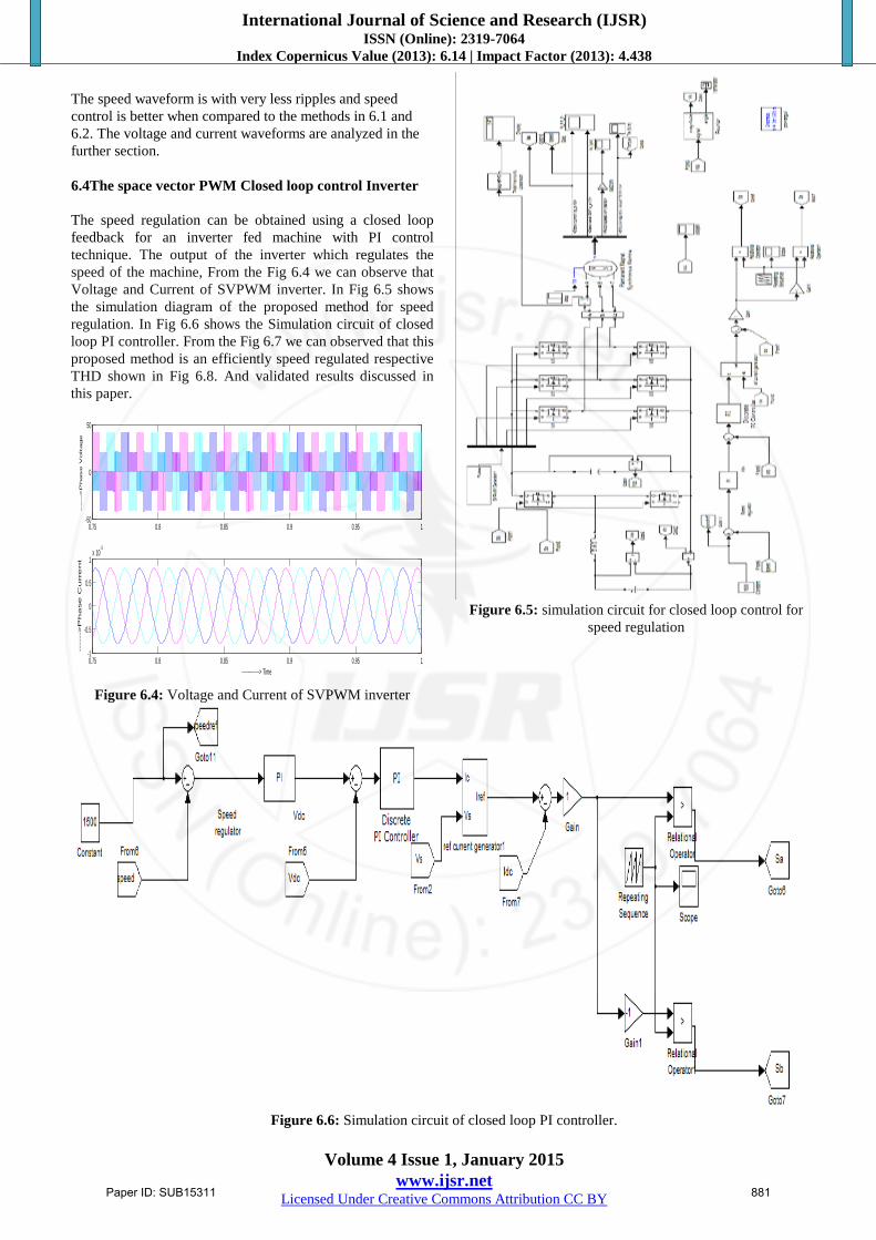
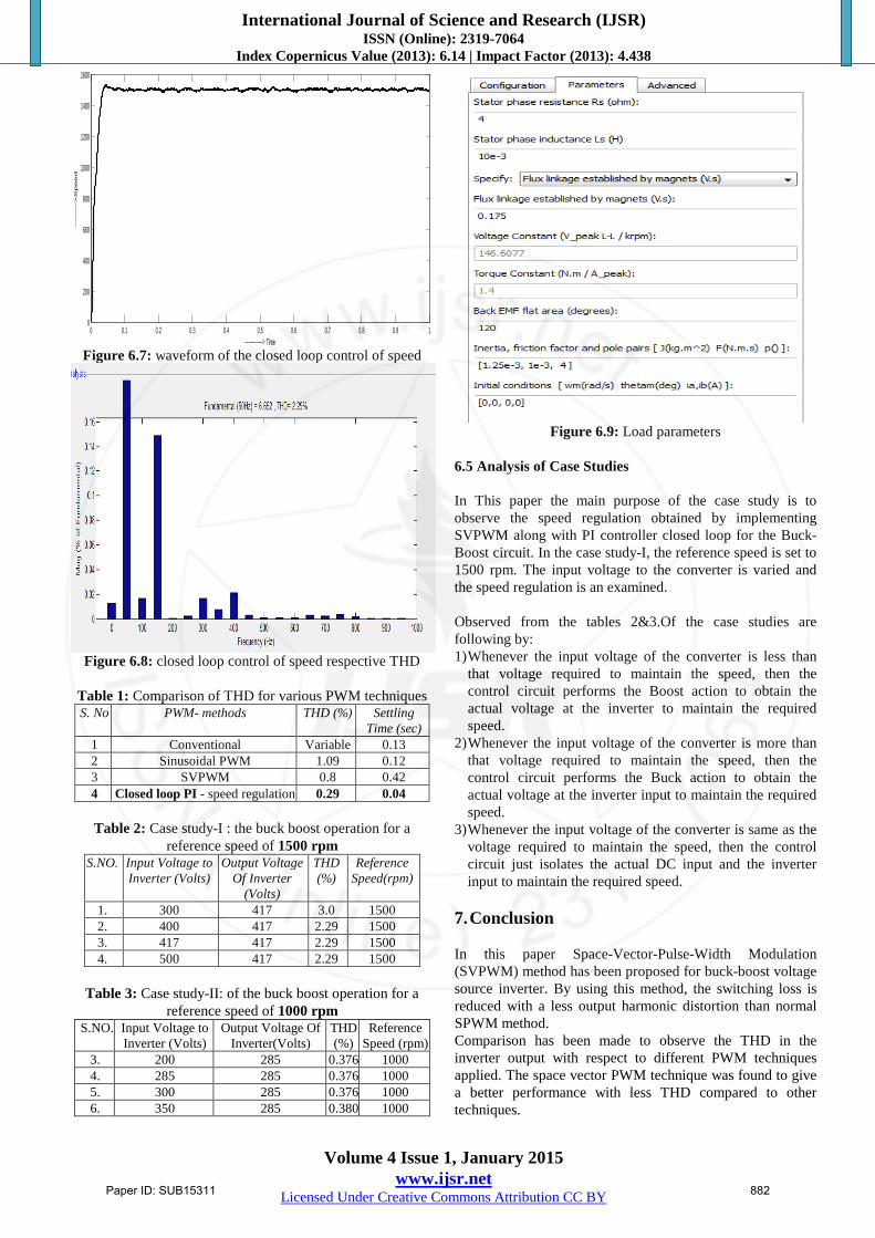
The speed waveform is with very less ripples and speed control is better when compared to the methods in 6.1 and 6.2. The voltage and current waveforms are analyzed in the further section. 6.4The space vector PWM Closed loop control Inverter The speed regulation can be obtained using a closed loop feedback for an inverter fed machine with PI control technique. The output of the inverter which regulates the speed of the machine, From the Fig 6.4 we can observe that Voltage and Current of SVPWM inverter. In Fig 6.5 shows the simulation diagram of the proposed method for speed regulation. In Fig 6.6 shows the Simulation circuit of closed loop PI controller. From the Fig 6.7 we can observed that this proposed method is an efficiently speed regulated respective THD shown in Fig 6.8. And validated results discussed in this paper.
0.75 0.8 0.85 0.9 0.95 1-50
0
50
----
-->
Phase V
oltage
0.75 0.8 0.85 0.9 0.95 1-1
-0.5
0
0.5
1x 10
-3
--------------> Time
----
-->
Ph
ase
Cu
rre
nt
Figure 6.4: Voltage and Current of SVPWM inverter
Figure 6.5: simulation circuit for closed loop control for
speed regulation
Figure 6.6: Simulation circuit of closed loop PI controller.
Paper ID: SUB15311 881
International Journal of Science and Research (IJSR) ISSN (Online): 2319-7064
Index Copernicus Value (2013): 6.14 | Impact Factor (2013): 4.438
Volume 4 Issue 1, January 2015 www.ijsr.net
Licensed Under Creative Commons Attribution CC BY
0 0.1 0.2 0.3 0.4 0.5 0.6 0.7 0.8 0.9 10
200
400
600
800
1000
1200
1400
1600
--------------> Time
----
----
->S
peed
Figure 6.7: waveform of the closed loop control of speed
Figure 6.8: closed loop control of speed respective THD
Table 1: Comparison of THD for various PWM techniques S. No PWM- methods THD (%) Settling
Time (sec) 1 Conventional Variable 0.13 2 Sinusoidal PWM 1.09 0.12 3 SVPWM 0.8 0.42 4 Closed loop PI - speed regulation 0.29 0.04
Table 2: Case study-I : the buck boost operation for a
reference speed of 1500 rpm S.NO. Input Voltage to
Inverter (Volts) Output Voltage
Of Inverter (Volts)
THD (%)
Reference Speed(rpm)
1. 300 417 3.0 1500 2. 400 417 2.29 1500 3. 417 417 2.29 1500 4. 500 417 2.29 1500
Table 3: Case study-II: of the buck boost operation for a
reference speed of 1000 rpm S.NO. Input Voltage to
Inverter (Volts) Output Voltage Of
Inverter(Volts) THD (%)
Reference Speed (rpm)
3. 200 285 0.376 1000 4. 285 285 0.376 1000 5. 300 285 0.376 1000 6. 350 285 0.380 1000
Figure 6.9: Load parameters
6.5 Analysis of Case Studies In This paper the main purpose of the case study is to observe the speed regulation obtained by implementing SVPWM along with PI controller closed loop for the Buck-Boost circuit. In the case study-I, the reference speed is set to 1500 rpm. The input voltage to the converter is varied and the speed regulation is an examined. Observed from the tables 2&3.Of the case studies are following by: 1) Whenever the input voltage of the converter is less than
that voltage required to maintain the speed, then the control circuit performs the Boost action to obtain the actual voltage at the inverter to maintain the required speed.
2) Whenever the input voltage of the converter is more than that voltage required to maintain the speed, then the control circuit performs the Buck action to obtain the actual voltage at the inverter input to maintain the required speed.
3) Whenever the input voltage of the converter is same as the voltage required to maintain the speed, then the control circuit just isolates the actual DC input and the inverter input to maintain the required speed.
7. Conclusion In this paper Space-Vector-Pulse-Width Modulation (SVPWM) method has been proposed for buck-boost voltage source inverter. By using this method, the switching loss is reduced with a less output harmonic distortion than normal SPWM method. Comparison has been made to observe the THD in the inverter output with respect to different PWM techniques applied. The space vector PWM technique was found to give a better performance with less THD compared to other techniques.
Paper ID: SUB15311 882
International Journal of Science and Research (IJSR) ISSN (Online): 2319-7064
Index Copernicus Value (2013): 6.14 | Impact Factor (2013): 4.438
Volume 4 Issue 1, January 2015 www.ijsr.net
Licensed Under Creative Commons Attribution CC BY
Instead of using a constant DC input to the inverter, a buck boost converter has been connected at the front end of the inverter. Therefore the same circuit can be employed for different AC loads connected to the inverter. The inverter output voltage can be varied according to the load requirements by varying the input to the inverter. The PWM technique along with the closed loop control using the PI controller has lead to the reduction of the THD. By implementing this technique to the inverter which feed the AC machines so as to control the speed and torque. The ripples in the speed waveform are very less and also in this compared to open loop PWM techniques. This paper validated results are an examined with less settling time and less harmonics in the output. 8. Future Scope The proposed SVPWAM modulation method has only been verified on the voltage source inverter, thus the future work should be done with the buck-boost current source inverter for multilevel, such as current-fed quasi-Z-source inverter topology. The discontinuous operation mode needs to be explored further to see if it can be utilized in order to bring some good features for the inverter. References
[1] Q. Lei and F. Z. Peng, “Space Vector Pulsewidth
Amplitude Modulation for a Buck-Boost Voltage/Current Source Inverter,” IEEE transactions on power electronics, vol 29, no. 1, Jan 2014.
[2] D. M. Divan and G. Skibinski, “Zero-switching-loss inverters for high power applications,” IEEE Trans. Ind. Appl., vol. 25, no. 4, pp. 634–643, Jul./Aug. 1989.
[3] W.McMurray, “Resonant snubbers with auxiliary switches,” IEEE Trans. Ind. Appl., vol. 29, no. 2, pp. 355–362, Mar./Apr. 1993.
[4] J.-S. Lai, R. W. Young, Sr., G. W. Ott, Jr., J. W. McKeever, and F. Z. Peng, “A delta-configured auxiliary resonant snubber inverter,” IEEE Trans. Ind.Appl., vol. 32, no. 3, pp. 518–525, May/Jun. 1996.
[5] J. S. Kim and S. K. Sul, “New control scheme for ac-dc-ac converter without dc link electrolytic capacitor,” in Proc. 24th Annu. IEEE PowerElectron. Spec. Conf., Jun. 1993, pp. 300–306.
[6] K. Rigbers, S. Thomas, U. Boke, and R. W. De Doncker, “Behavior and loss modeling of a three-phase resonant pole inverter operating with 120°A double flattop modulation,” in Proc. 41st IAS Annu. Meeting IEEE Ind.Appl. Conf., Oct. 8–12, 2006, vol. 4, pp. 1694–1701.
[7] J. Shen, K Rigbers, C. P. Dick, and R. W. De Doncker, “A dynamic boost converter input stage for a double 120◦ flattop modulation based three phase inverter,” in Proc. IEEE Ind. Appl. Soc. Annu. Meeting, Oct. 5–9, 2008, pp. 1–7.
[8] H. Fujita, “A three-phase voltage-source solar power conditioner using a single-phase PWM control method,” in Proc. IEEE Energy Convers.Congr.Expo., 2009, pp. 3748–3754.
[9] H. Haga, K. Nishiya, S. Kondo, and K. Ohishi, “High power factor control of electrolytic capacitor less current-fed single-phase to three-phase power converter,” in Proc. Int. Power Electron. Conf., Jun. 21–24, 2010, pp. 443–448.
[10] X.Chen and M. Kazerani, “Space vectormodulation control of an ac-dc-ac converter with a front-end diode rectifier and reduced dc-link capacitor,” IEEE Trans. Power Electron., vol. 21, no. 5, pp. 1470–1478, Sep. 2006.
[11] M. Hinkkanen and J. Luomi, “Induction motor drives equipped with diode rectifier and small dc-link capacitance,” IEEE Trans. Ind. Electron., vol. 55, no. 1, pp. 312–320, Jan. 2008.
Author Profile
S. Narasimha born on 10th Aug 1979, obtained B.Tech degree in 2003 and M.Tech degree in 2009 with a specialization in Power Electronics & Industrial Drives from JNTUHCEH, INDIA. Research Scholar in Dept Of EEE, JNTUH.
M. Sushama, born on 8th Feb 1973, .Obtained her B.Tech degree in 1993 and M.Tech degree in 2003 with a specialization in Electrical Power Systems from JNTU, INDIA. She obtained her Ph.D. from JNTU Hyderabad, India in 2009 in the area of “Power
Quality” using Wavelet Transforms Presently she is working as Professor in the Department of EEE, JNTUH College of Engineering, Kukatpally, Hyderabad.
Paper ID: SUB15311 883