CHAPTER 3 DESIGN, MODELLING AND IMPLEMENTATION OF BOOST...
25
70 CHAPTER 3 DESIGN, MODELLING AND IMPLEMENTATION OF BOOST CONVERTER WITH OBSERVER CONTROLLER 3.1 OVERVIEW In this chapter the derivation of state feedback gain matrix for Boost converter under both continuous time domain and discrete time domain are explained using pole placement method. Similar to the Observer controller for Buck converter, the derivation of the observer controller for the Boost converter under both the continuous and discrete time domain is derived. The simulation and results are also presented. 3.2 DESIGN AND MODELLING OF BOOST CONVERTER In this section the design and state space modelling of the Boost converter is explained and the schematic diagram of a Boost converter is shown in the Figure 3.1. In this converter, the output voltage is always greater than the input voltage. It has a very simple structure, continuous input current, step up conversion ratio and it also has a clamped voltage stress and more over clamped switch voltage stress to the output voltage. Figure 3.1 Schematic diagram of the Boost converter
Transcript of CHAPTER 3 DESIGN, MODELLING AND IMPLEMENTATION OF BOOST...

70
CHAPTER 3
DESIGN, MODELLING AND IMPLEMENTATION OF
BOOST CONVERTER WITH OBSERVER CONTROLLER
3.1 OVERVIEW
In this chapter the derivation of state feedback gain matrix for
Boost converter under both continuous time domain and discrete time domain
are explained using pole placement method. Similar to the Observer controller
for Buck converter, the derivation of the observer controller for the Boost
converter under both the continuous and discrete time domain is derived. The
simulation and results are also presented.
3.2 DESIGN AND MODELLING OF BOOST CONVERTER
In this section the design and state space modelling of the Boost
converter is explained and the schematic diagram of a Boost converter is
shown in the Figure 3.1. In this converter, the output voltage is always greater
than the input voltage. It has a very simple structure, continuous input current,
step up conversion ratio and it also has a clamped voltage stress and more over clamped switch voltage stress to the output voltage.
Figure 3.1 Schematic diagram of the Boost converter

71
The output voltage is given by,
= (3.1)
The inductor and capacitor values of the Boost converter are
derived by having the same assumption as that of the Buck converter. Now
the critical value of the inductor LC which decides the condition for the
continuous current mode of the operation is given by,
= ( ) (3.2)
where fs is the switching frequency. The inductor value is determined by using
the following equation,
= (3.3)
Similarly the capacitor value can be determined by assuming
appropriate ripple voltage and by substituting the necessary values in the
following equation,
= (3.4)
In this type of converter, a very high peak current flows through the
switch. It is very difficult to attain the stability of this converter due to high
sensitivity of the output voltage to the duty cycle variations. When compared
to Buck converter the inductor and capacitor sizes are larger since high RMS
current would flow through the filter capacitor.
Based on the above discussion the parameters designed for Boost
Converter is shown in Table 3.1.

72
Table 3.1 Design values of Boost converter
Sl.No Parameters Design Values
1 Input Voltage 24 V
2 Output Voltage 50 V
3 Inductance, L 72 µH
4 Capacitance, C 216.9X10⁻⁶ F
5 Load Resistance, R 23
6 Switching frequency, fs 20 kHz
The design details of Boost converter are perceived above and
using the designed values the open loop response of the Boost converter is
obtained and shown in the Figure 3.2, where the peak overshoot and steady
error are found to be maximum. The voltage ripples are also observed which
requires the design of closed loop control.
Figure 3.2 Open loop response of Boost converter

73
The differential equations describing the Boost converter can be
explained in the following section by assuming two modes of operation. The
inductor current, iL and the capacitor voltage, Vo are the state variables. The
semiconductor Switch is in on condition for the time interval , 0 t Ton and
hence the inductor L gets connected to the supply and stores the energy. Since
the diode is in off condition, the output stage gets isolated from the supply.
Here the inductor current flows through the inductor and completes its path
through the source. The equivalent circuit for this mode is shown in the
Figure 3.3.
Figure 3.3 Equivalent circuit of Boost converter for mode 1
Applying Kirchoff’s laws, the following equations describing
mode1 are obtained as,
=
= (3.5)
Now the coefficient matrices for this mode are obtained as,
0 00 (3.6)
0 (3.7)

74
During the time interval Ton t T, the diode is in on state and the
switch is in off state and hence the energy from the source as well as the
energy stored in the inductor is fed to the load. The inductor current flows
through the inductor L, the capacitor C, the diode and the load. The equivalent
circuit for this mode is shown in Figure 3.4.
Figure 3.4 Equivalent circuit of Boost converter for mode 2
Applying Kirchoff’s laws, the following equations describing
mode 2 are obtained,
=
= (3.8)
The coefficient matrices for this mode is defined as follows,
0 (3.9)
0 (3.10)
The output voltage Vo (t) across the load is expressed as,
( ) = [0 1] ) (3.11)

75
Thus the design and modelling of the Boost converter has been
done which further leads to the design of Observer controller. In the next
section, the derivation of the state feedback matrix for the Boost converter is
carried out which is the first step for the design of Observer controller transfer
function. By substituting the values of L and C thus designed, the state
coefficient matrices for the Boost converter is obtained as follows:
= 0 6944.336944.33 200 (3.12)
= 13.8887 × 100
(3.13)
= [0 1] (3.14)
= [0] (3.15)
3.3 DERIVATION OF STATE FEEDBACK MATRIX FOR THE
BOOST CONVERTER
The general derivation of the state feedback matrix for the DC-DC
converter has already been discussed in detail in chapter 2. Now in this
section, the state feedback gain matrix for the Boost converter is explained as
follows. The root locus of the Boost converter under continuous time is drawn
as shown in the Figure 3.5. The open loop poles of the Boost converter is
shown by cross in the figure. The desired poles are arbitrarily placed in order
to obtain the state feedback matrix.

76
Figure 3.5 Root locus of Boost converter in s-domain
The derivation of the state feedback matrix for the Boost converter
is carried out in the same manner as that for the Buck converter using pole
placement technique which has already been explained in the second chapter.
Now, the state feedback matrix for the Boost converter is derived as follows:
Step1: The characteristic polynomial to find the unknown values of
[ ] is formed as follows:
| ( )| = + (200 + 13.8887 × 10 )
+2.7777 × 10 + 96.4470 × 10 + 48.2237 × 10 = 0 (3.16)
Step 2: The desired characteristic equation is formed by arbitrarily placing
the poles as follows:
+ 14.2042 × 10 + 57.97459 × 10 = 0 (3.17)
By equating the like powers of s in the Equations (3.16) and (3.17),
the state feedback matrices are obtained as k1 = 1.008 and k2 = 0.07206.

77
In order to check the robustness of the control law, the step input is
used and the output response has been illustrated in the Figure 3.6. From the
Figure 3.6, it is very well understood that the system settles down faster and
the state feedback matrix is capable enough to realize the stability of the
Boost converter.
Figure 3.6 Step response of the Boost converter in continuous time domain
A similar case can be derived for the Boost converter under discrete
time domain also and it is explained now. The state equations for the Boost
converter under discrete time domain is defined as,
= 0.9405 0.33860.3386 0.9308 (3.18)
= 0.68060.1190 (3.19)
= [0 1] (3.20)
= [0] (3.21)

78
As per the Nyquist criterion which states that sampling frequency
of the analog signal should be atleast twice the maximum signal frequency,
the sampling frequency is assumed as 1 MHz. The digital state feedback
matrix can be derived in the same method as that for the continuous domain
excepting the domain considered here is z. The root locus of Boost converter
in z domain is drawn as shown in the Figure 3.7. The desired poles are chosen
arbitrarily in order to find the digital state feedback matrix. The open loop
poles are shown by cross in the figure. The stability of the converter is
obtained in such a way by moving the poles towards the left half of the
z-plane. More the poles are moved towards the left hand side, more stability
of the converter is obtained.
Figure 3.7 Root locus of the Boost converter in z-domain
The digital state feedback matrix can be obtained by substitution
method and is explained as follows:
Step1: The characteristic polynomial to find the unknown values of
[ ] is formed as follows:

79
| ( )| = + (0.6806 1.8713)
0.6335 + 0.04029 + 0.99007 = 0 (3.22)
Step 2: The desired characteristic equation is formed by arbitrarily placing
the poles as follows:
0.6094 0.1442 = 0 (3.23)
By equating the like powers of s in the Equations (3.22) and (3.23),
the state feedback matrices are obtained as kd1 = 1.854 and kd2 = 1.
In order to check the robustness of the control law, the step input is
used and the output response has been demonstrated in the Figure 3.8. It is
clear that the system settles down faster and the digital state feedback matrix
is efficient enough to obtain the stability of the Boost converter.
Figure 3.8 Step response of the Boost converter in discrete time domain
Thus the state feedback matrix for the Boost converter under both
continuous time and discrete time domain are derived and also the suitability
of these matrices to obtain the stability of the Boost converter is illustrated

80
clearly in this section. Now the derivation of the observer gain matrix for the
Boost converter under both continuous and discrete time domain has been
dealt in the following section.
3.4 DERIVATION OF OBSERVER GAIN MATRIX FOR BOOST
CONVERTER
The general derivation of full order state observer gain matrix for
DC-DC converter has already been explained in the second chapter. Now, for
the Boost converter this matrix can be derived by the substitution method by
assuming appropriate natural frequency of oscillation and damping ratio as
per the thumb rule. By assuming the damping ratio, = 0.6 and the natural
frequency of oscillation, n = 12.02788 x 10³ rad/sec, the desired
characteristic equation can be obtained as follows,
+ 173.2015 × 10 + 2.08324 × 10 = 0 (3.24)
The polynomial equation with unknown values of observer poles is
given by,
+ (200 + ) + (48.2237 × 10 + 6944.33 ) = 0 (3.25)
Comparing the Equations (3.24) and (3.25), the observer gain matrix
is obtained. The values are = 2992.9 × 10 = 173.0015 × 10 .
Since the observer poles are mainly designed to check the
robustness of the control law, it is essential that the estimated state variables
and error variables of the Boost converter should converge at zero from any
non-zero initial value. This ensures the asymptotic stability of the converter
under consideration with the desired pole locations. It is demonstrated in the
Figures 3.9 to 3.12 respectively. All the variables such as x1, x2, e1 and e2
under consideration attain zero value from any non zero value thereby
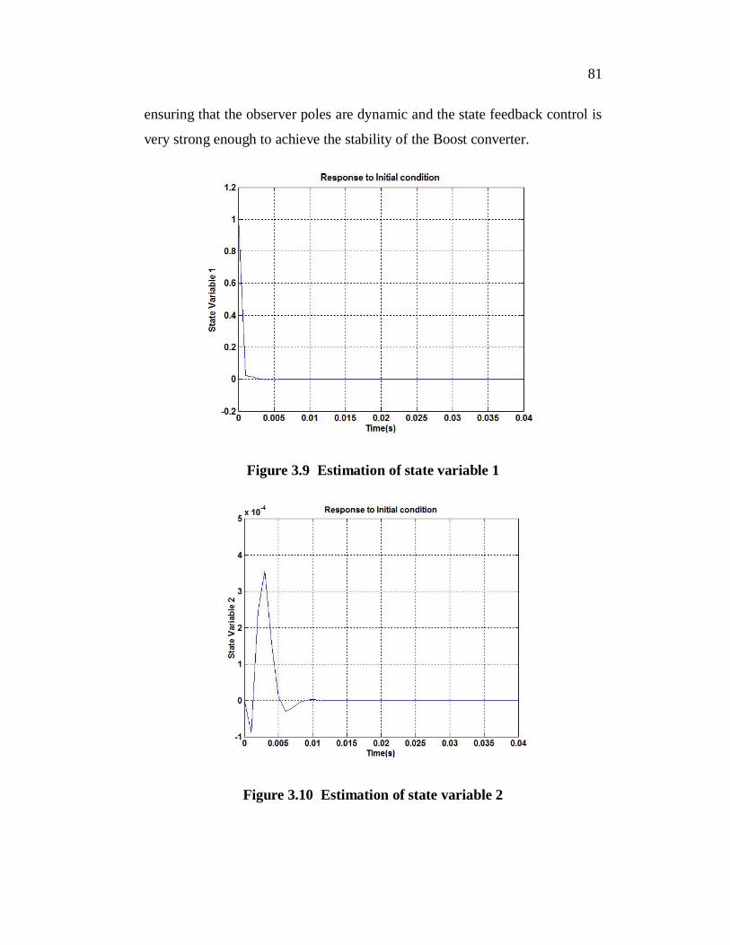
81
ensuring that the observer poles are dynamic and the state feedback control is
very strong enough to achieve the stability of the Boost converter.
Figure 3.9 Estimation of state variable 1
Figure 3.10 Estimation of state variable 2

82
Figure 3.11 Estimation of error variable 1
Figure 3.12 Estimation of error variable 2
Thus the observer gain matrix for the Boost converter is designed
and it also has been checked for its dynamic constancy. Now, by using the
Separation principle which has already been explained in chapter 2, the
transfer function of the observer controller for the Boost converter under

83
continuous time domain is obtained by the substitution of the state feedback
gain matrix, k and observer gain matrix, g in the appropriate observer
controller transfer function given by Equation (2.76) as follows,
( ) = . × . ×. . ×
(3.26)
Similar case can be derived for the discrete time system and it is
discussed now. By assuming the damping ratio, = 0.5, sampling time Ts = 1 µs
and the natural frequency of oscillation, n = 192.4461 x 10³ rad/sec, the
desired characteristic equation can be obtained as follows,
= ± = . × . × × ×
× (± . × × × × . ) (3.27)
The above equation can be simplified as,
7.50449 × 10 + 6.6235 × 10 = 0 (3.28)
The polynomial equation with unknown values of observer poles is
given by
+ ( 1.8713) + (0.3386 0.9405 + 0.990067) = 0 (3.29)
Comparing the Equations (3.28) and (3.29), the observer gain
matrix is obtained. The values are = 2.2948 = 1.8788.
By using the Separation principle which has already been explained
in chapter 2, the transfer function of the prediction observer controller for the
Boost converter under discrete time domain is obtained by substituting the
values of digital state feedback control matrix and observer gain matrix in the
Equation (2.84) as follows,

84
( ) = . .. .
(3.30)
3.5 RESULTS AND DISCUSSION
3.5.1 Boost Converter (Continuous Time Domain)
The previous sections clearly explain the derivation of the Observer
controller for the Boost converter under both continuous and discrete time
domain. Now the simulation results are exemplified and are discussed in
detail. The design and the performance of Boost converter is accomplished in
continuous conduction mode and simulated using MATLAB/ Simulink. The
ultimate aim is to achieve a robust controller for the Boost converter inspite of
uncertainty and large load disturbances. The performance parameters of the
Boost converter under consideration are rise time, settling time, maximum
peak overshoot and steady state error, which are shown in the Table 3.2. It is
evident that the converter settles down at 0.015 s and the rise time of the
converter is 0.01s. No overshoots or undershoots are evident and no steady
state error is observed. The simulation of the Boost converter is also carried
out by varying the load, not limiting it to R load and it is illustrated in the
Table 3.3.
Table 3.2 Performance parameters of Boost converter (Continuous time domain)
Sl.No Parameters Values
1 Settling Time (s) 0.015
2 Peak Overshoot (%) 0
3 Steady State Error (V) 0
4 Rise Time (s) 0.01
5 Output Ripple Voltage 0

85
Table 3.3 Output response of Boost converter for load variations (Continuous time domain)
Sl. No Load Reference
Voltage (V)
Output Voltage
(V)R( ) L(H) E(V)
1 25 -- -- 50 50.002 30 -- -- 50 50.013 25 1 x 10⁻⁶ -- 50 50.004 25 100 x 10-6 -- 50 50.055 20 1 x 10⁻⁶ 5 50 50.046 20 50 x 10-6 5 50 50.20
It is obviously understood that the Boost converter with observer
controller is efficient enough to track the output voltage irrespective of the
load variations. When the load resistance is varied as 25 and 30 , the
converter is able to track the output voltages as 50 V and 50.01 V respectively
for the reference voltage of about 50 V. Again when the inductance of 1µH
and 100 µH are added to the resistance of 25 , the output thus obtained is of
the order of 50 V and 50.05 V respectively. The steady state error observed is
of very minimum of about 0.05 V. The simulation is also carried out again
using RLE load with a resistance of 20 , two different inductances of 1 µH
and 50 µH and an ideal voltage source of about 5 V. The response of the
converter is such that the controller is capable to work under all the load
transients thereby tracking the voltage as 50.04 V and 50.20 V respectively.
The simulation is also carried out by varying the input voltage and
load resistance and the corresponding, input voltage, load resistance, output
voltage, inductor current and load current are shown in the Figure 3.13. The
input voltage is first set as 24 V until 0.4 s and again varied from 24 V to
22 V upto 0.6 s. Again at 0.6 s it is varied to 24 V and at 0.8 s it has been
varied to 26 V respectively.

86
Figure 3.13 Output response of Boost converter with observer controller (Vs – Input Voltage, Ro – Load resistance, Vo – Output Voltage,
IL – Inductor current, Io – Load Current)
Simultaneously the load resistance is also varied from 20 to 19
and again to 18.5 respectively at 0.3 s and 0.6 s. The corresponding output
response of the Boost converter shows fixed output voltage regulation.
Undershoots and Overshoots are not observed and the steady state error is
also not apparent. The inductor current and load current are also shown in the
Figure 3.13, which shows minimum amount of current ripples. In order to
check the dynamic performance of the system, the L and C parameters of the
Boost converter are varied and the output response of the system is shown in
the Table 3.4.

87
Table 3.4 Output response of Boost converter with variable converter parameters (Continuous time domain)
Sl.No Inductance, L Capacitance, CReference Voltage(V)
Output Voltage (V)
1 100 µH 220 µF 50 49.852 150 µH 200 µF 50 50.343 200 µH 150 µF 50 49.964 250 µH 100 µF 50 50.105 250 µH 250 µF 50 50.24
The inductance of the Boost converter is varied as, 100 µH,
150 µH, 200 µH and 250 µH and the corresponding capacitor values are set
as 220 µF, 200 µF, 150 µF, 100 µF and 250 µF respectively. It is understood
from the Table 3.4 that the system is very much dynamic in tracking the
reference voltages inspite of the variations in the inductance and capacitance
values. The system does not show any overshoots or undershoots and it settles
down fast with a settling time of about 0.015 s for all the values. The steady
state error thus noticeable ranges between 0.3% and 0.6% which is considered
as within the tolerable limits. The load current, output power, losses and
efficiency of the Boost converter with Observer controller is determined and
is illustrated in Table 3.5.
Table 3.5 Efficiency of the Boost converter with analog observer controller
Sl. No. IO(A) PO(W) Losses(W) Efficiency (%) 1 1.5455 77.3368 1.9098 97.5902 1.9723 98.7136 2.3662 97.6593 2.1755 108.8185 3.5067 96.8784 2.3750 118.6313 4.2135 96.5705 2.5170 126.1017 5.6936 95.6806 4.4590 222.8608 12.7787 94.577

88
The efficiency of the Boost converter remains more or less same
with the increase in the load current. It is very well understood that the Boost
converter with Observer controller is highly efficient and the highest
efficiency is obtained as 97.659% at a load current of about 1.9723 A and the
corresponding output power is 98.7136 W. The simulation for Boost
converter with prediction observer controller is carried out in the same
manner as explained in the above section and is presented in the following
section.
3.5.2 Boost Converter (Discrete Time Domain)
Simulation has been carried out for the Boost converter with
prediction observer controller under discrete time domain and the
performance parameters are tabulated in Table 3.6. The system settles down
much faster at 0.0075 s and the rise time is only 0.004 s as shown in the
Table 3.6. The overshoots and undershoots are not seen and there is no peak
overshoot.
Table 3.6 Performance parameters of Boost converter (Discrete time domain)
Sl. No. Parameters Values
1 Settling Time (s) 0.0075
2 Peak Overshoot (%) 0
3 Steady State Error (V) 0
4 Rise Time (s) 0.004
5 Output Ripple Voltage 0
The output response with load variations is shown in the Table 3.7.
When the load resistance is varied as 25 and 30 , the Boost converter with

89
discrete controller is capable to track the output voltages as 50.02 V and
49.95 V respectively for the reference voltage of about 50 V. Again when the
inductance of 1 µH and 100 µH are added to the resistances of 25 , the
output thus obtained is of the order of 49.99 V and 49.79 V respectively. The
steady state error observed is of very lesser of the order of about 0.01 V and
0.21 V respectively. The simulation is also carried out again using RLE load
with a resistance of 20 , two inductances of 1 µH and 50 µH and an ideal
voltage source of about 5 V. The response of the converter is such that the
controller is proficient to work under all the load transients thereby tracking
the voltage as 50.03 V and 49.89 V respectively.
Table 3.7 Output response of Boost converter for load variations (Discrete time domain)
Sl.NoLoad Reference
Voltage(V)Output
Voltage (v)R( ) L(H) E(V)1 25 -- -- 50 50.02
2 30 -- -- 50 49.95
3 25 1x10⁻⁶ -- 50 49.99
4 25 100x 10-6 -- 50 49.79
5 20 1x10⁻⁶ 5 50 50.03
6 20 50x10-6 5 50 49.89
The simulation is also carried out by varying the input voltage and
load resistance and the corresponding, input voltage, load resistance, output
voltage, inductor current and load current are shown in the Figure 3.14. The
input voltage is first set as 24 V until 0.01 s and again varied to 22 V upto
0.02 s. Again at 0.02 s it is varied to 24 V and at 0.03 s it has been varied to
26 V up to 0.04 s and again varied to 24 V respectively till 0.05 s.
Simultaneously the load resistance is also varied as 22 , 20 and 10

90
respectively and the corresponding output response of the Boost converter
thus obtained shows tight output voltage regulation. Undershoots and
Overshoots are not observed and the steady state error is also not evident. The
inductor current and load current which are also shown, shows no evidence of
current ripples. In order to check the dynamic performance of the system, the
L and C parameters of the Boost converter are varied and the output response
of the system is shown in the Table 3.8.
Table 3.8 Output response of Boost converter with variable converter parameters (Discrete time domain)
Sl.NoInductance,
LCapacitance,
CReference Voltage(V)
Output Voltage (V)
1 100 µH 220 µF 50 49.95
2 150 µH 200 µF 50 50.04
3 200 µH 150 µF 50 49.89
4 250 µH 100 µF 50 50.10
5 250 µH 250 µF 50 50.06
The inductance and the capacitance values are changed in the same
manner as that for the analog controller as shown in the Table 3.8. It is
obvious from the Table 3.8 that the system is very much dynamic in tracking
the reference voltages inspite of the variations in the inductance and
capacitance values. The system does not show any overshoots or undershoots
and it settles down fast with a settling time of about 0.01 s for all the values.
The steady state error thus noticeable is within the tolerable limits ranging
from 0.2% to 0.6%.

91
Figure 3.14 Output response of Boost converter with prediction observer controller (Vs – Input Voltage, Ro – Load resistance, Vo – Output Voltage, IL – Inductor current, Io – Load Current)
The load current, output power, losses and efficiency of the Boost
converter is determined and is illustrated in Table 3.9. The efficiency of the
Boost converter with Prediction Observer controller remains more or less
same with the increase in the load current. It is very well understood that the
system is highly efficient and the highest efficiency is obtained as 98.659% at
a load current of about 1.342 A and the corresponding output power is
98.674 W.

92
Table 3.9 Efficiency of the Boost converter with prediction observer controller
Sl. No. Io(A) Po(W) Losses(W) Efficiency(%)
1 1.5455 77.04 1.1018 98.590
2 1.9723 98.674 1.3412 98.659
3 2.1755 108.775 2.3582 97.878
4 2.3750 118.798 2.9587 97.570
5 2.5170 125.850 4.3217 96.680
6 4.4590 223.396 7.9179 96.577
The efficiency of the Boost converter under both continuous and
discrete time domain drawn against the load current is shown compared in the
Figure 3.15. The efficiency of the Boost converter with prediction observer
controller shows improved results when compared with its analog counterpart.
Figure 3.15 Comparison of efficiencies of Boost converter
The Boost converter with prediction controller has been efficient
enough in such a way that it is capable of tracking the reference voltages of
50 V and 60 V inspite of the input voltage variations. The input voltage is
75
80
85
90
95
100
1.5 2.5 3.5 4.5
Effic
ienc
y(%
)
Load Current (A)
Analog controller
DiscreteController

93
varied as 24 V till 0.01 s and at 0.01 s it is varied as 22 V and again it is
varied as 24 V and 26 V at 0.02 s and 0.03 s respectively. Finally it is varied
as 24 V at 0.04 s. The reference values are varied as 50 V and 60 V and it is
illustrated in the Figure 3.16. In this figure green line represents the set value
and the blue line represents the actual output voltage.
Figure 3.16 Output response of Boost converter for variation in the reference voltages
3.6 CONCLUSION
A state feedback control approach has been designed for the Boost
converter under both continuous time domain and discrete time domain using
pole placement technique and separation principle. The full order state
observer has been designed to ensure robust control for the converter. The
separation principle allows designing a dynamic compensator which very
much looks like a classical compensator since the design is carried out using
simple root locus technique. The mathematical analysis and simulation study
show that the Boost converter with both analog and digital controller thus

94
designed achieves tight output voltage regulation, good dynamic
performances and higher efficiency.
In the next chapter the Observer controller for interleaved Buck
converter is designed.