Interconnect Metallization - Applied Materials
16
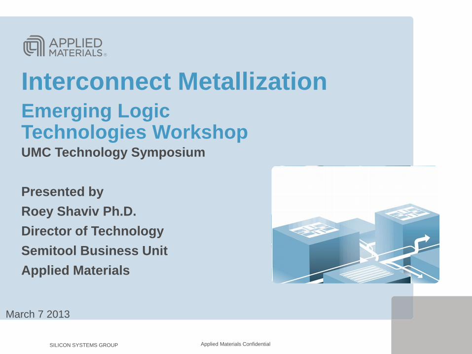
Applied Materials Confidential SILICON SYSTEMS GROUP Interconnect Metallization Emerging Logic Technologies Workshop UMC Technology Symposium Presented by Roey Shaviv Ph.D. Director of Technology Semitool Business Unit Applied Materials March 7 2013
Transcript of Interconnect Metallization - Applied Materials
Applied Materials Confidential SILICON SYSTEMS GROUP
Interconnect Metallization Emerging Logic Technologies Workshop UMC Technology Symposium
Presented by
Roey Shaviv Ph.D.
Director of Technology
Semitool Business Unit
Applied Materials
March 7 2013
Applied Materials Confidential
R 140
G 140
B 140
R 220
G 220
B 220
R 69
G 153
B 195
R 254
G 203
B 0
R 255
G 121
B 1
R 234
G 40
B 57
R 155
G 238
B 255
R 146
G 212
B 0
R 75
G 75
B 75
R 6
G 30
B 60
SILICON SYSTEMS GROUP
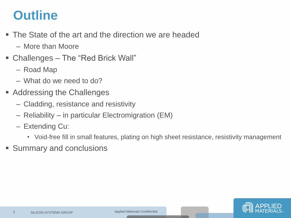
Outline
The State of the art and the direction we are headed
– More than Moore
Challenges – The “Red Brick Wall”
– Road Map
– What do we need to do?
Addressing the Challenges
– Cladding, resistance and resistivity
– Reliability – in particular Electromigration (EM)
– Extending Cu:
• Void-free fill in small features, plating on high sheet resistance, resistivity management
Summary and conclusions
2
Applied Materials Confidential
R 140
G 140
B 140
R 220
G 220
B 220
R 69
G 153
B 195
R 254
G 203
B 0
R 255
G 121
B 1
R 234
G 40
B 57
R 155
G 238
B 255
R 146
G 212
B 0
R 75
G 75
B 75
R 6
G 30
B 60
SILICON SYSTEMS GROUP
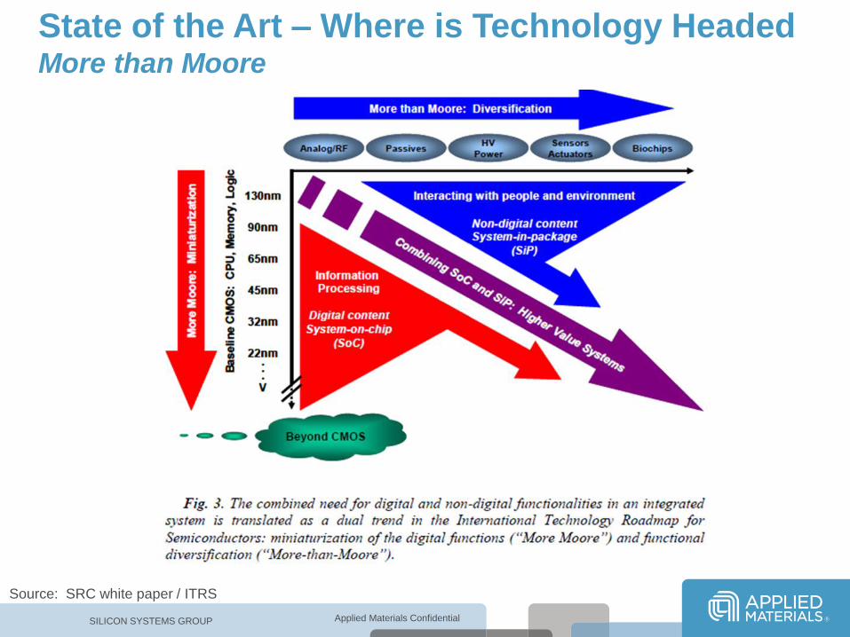
State of the Art – Where is Technology Headed More than Moore
Source: SRC white paper / ITRS
Applied Materials Confidential
R 140
G 140
B 140
R 220
G 220
B 220
R 69
G 153
B 195
R 254
G 203
B 0
R 255
G 121
B 1
R 234
G 40
B 57
R 155
G 238
B 255
R 146
G 212
B 0
R 75
G 75
B 75
R 6
G 30
B 60
SILICON SYSTEMS GROUP
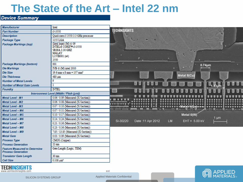
The State of the Art – Intel 22 nm
Applied Materials Confidential
R 140
G 140
B 140
R 220
G 220
B 220
R 69
G 153
B 195
R 254
G 203
B 0
R 255
G 121
B 1
R 234
G 40
B 57
R 155
G 238
B 255
R 146
G 212
B 0
R 75
G 75
B 75
R 6
G 30
B 60
SILICON SYSTEMS GROUP
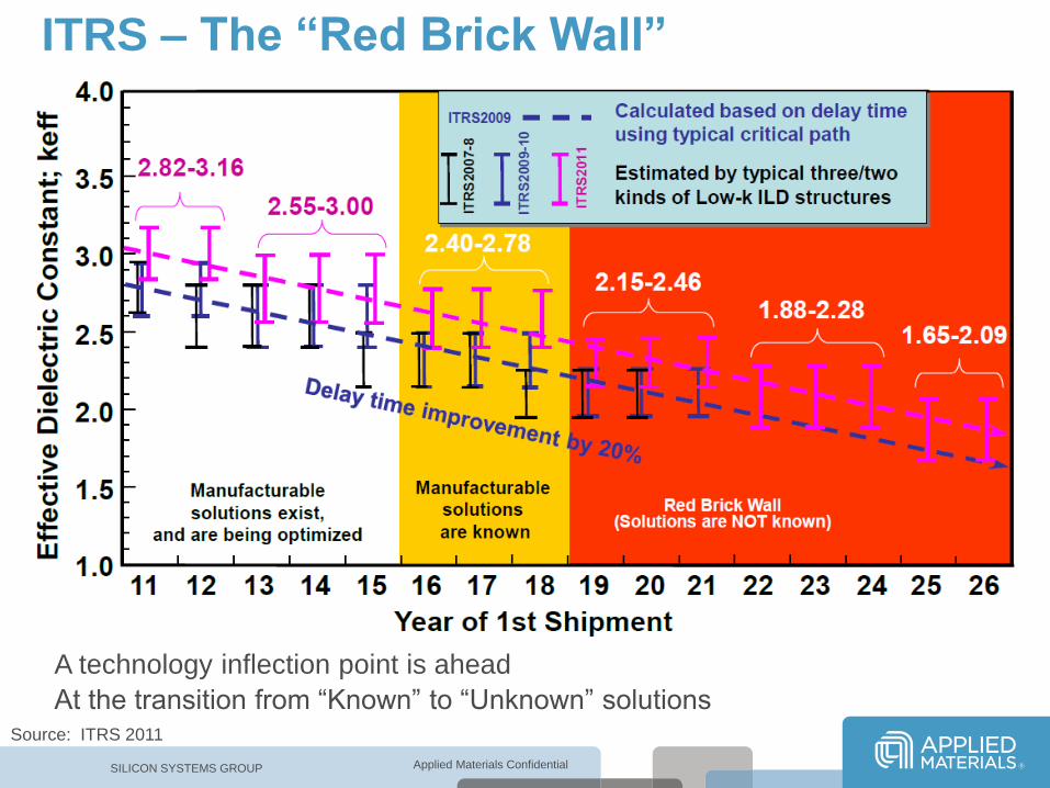
ITRS – The “Red Brick Wall”
Source: ITRS 2011
A technology inflection point is ahead
At the transition from “Known” to “Unknown” solutions
Applied Materials Confidential
R 140
G 140
B 140
R 220
G 220
B 220
R 69
G 153
B 195
R 254
G 203
B 0
R 255
G 121
B 1
R 234
G 40
B 57
R 155
G 238
B 255
R 146
G 212
B 0
R 75
G 75
B 75
R 6
G 30
B 60
SILICON SYSTEMS GROUP 6
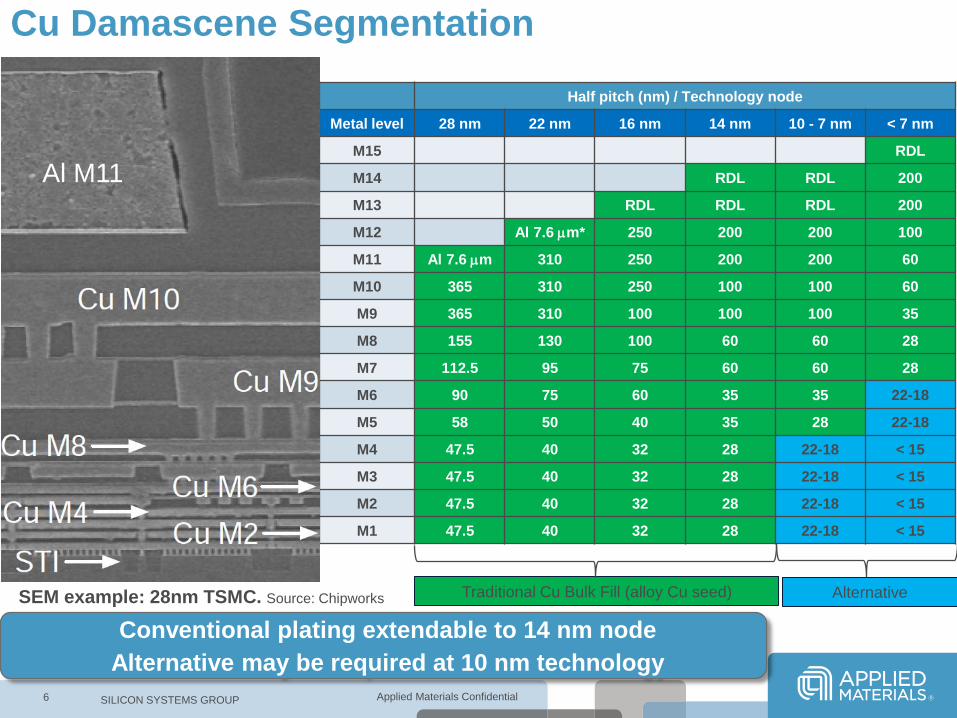
SEM example: 28nm TSMC. Source: Chipworks
Cu Damascene Segmentation
Half pitch (nm) / Technology node
Metal level 28 nm 22 nm 16 nm 14 nm 10 - 7 nm < 7 nm
M15 RDL
M14 RDL RDL 200
M13 RDL RDL RDL 200
M12 Al 7.6 mm* 250 200 200 100
M11 Al 7.6 mm 310 250 200 200 60
M10 365 310 250 100 100 60
M9 365 310 100 100 100 35
M8 155 130 100 60 60 28
M7 112.5 95 75 60 60 28
M6 90 75 60 35 35 22-18
M5 58 50 40 35 28 22-18
M4 47.5 40 32 28 22-18 < 15
M3 47.5 40 32 28 22-18 < 15
M2 47.5 40 32 28 22-18 < 15
M1 47.5 40 32 28 22-18 < 15
Traditional Cu Bulk Fill (alloy Cu seed) Alternative
Al M11
Conventional plating extendable to 14 nm node
Alternative may be required at 10 nm technology
Applied Materials Confidential
R 140
G 140
B 140
R 220
G 220
B 220
R 69
G 153
B 195
R 254
G 203
B 0
R 255
G 121
B 1
R 234
G 40
B 57
R 155
G 238
B 255
R 146
G 212
B 0
R 75
G 75
B 75
R 6
G 30
B 60
SILICON SYSTEMS GROUP 7
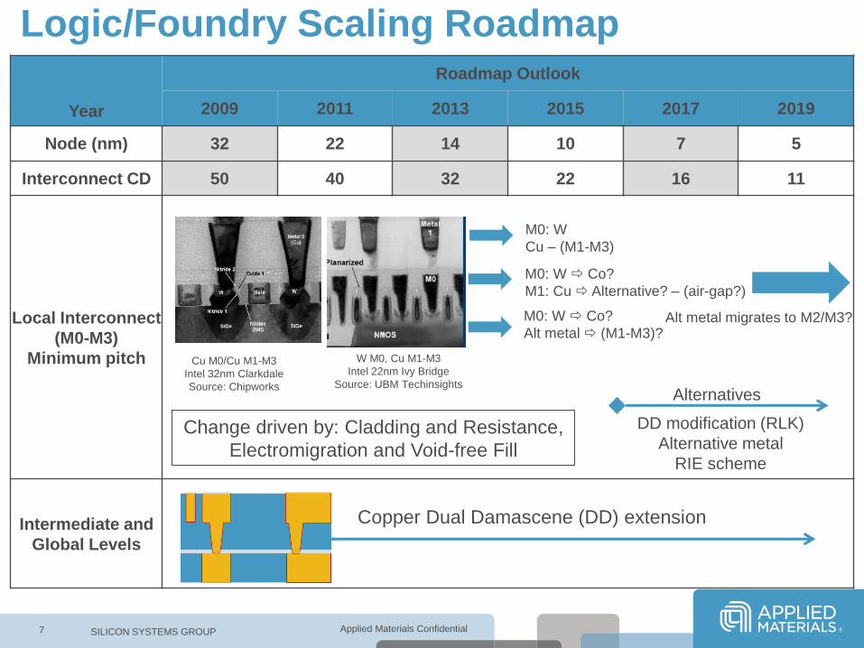
Year
Roadmap Outlook
2009 2011 2013 2015 2017 2019
Node (nm) 32 22 14 10 7 5
Interconnect CD 50 40 32 22 16 11
Local Interconnect
(M0-M3)
Minimum pitch
Intermediate and
Global Levels
Logic/Foundry Scaling Roadmap
Cu M0/Cu M1-M3
Intel 32nm Clarkdale
Source: Chipworks
W M0, Cu M1-M3
Intel 22nm Ivy Bridge
Source: UBM Techinsights
M0: W Co?
M1: Cu Alternative? – (air-gap?)
M0: W
Cu – (M1-M3)
M0: W Co?
Alt metal (M1-M3)? Alt metal migrates to M2/M3?
DD modification (RLK)
Alternative metal
RIE scheme
Alternatives
Copper Dual Damascene (DD) extension
Change driven by: Cladding and Resistance,
Electromigration and Void-free Fill
Applied Materials Confidential
R 140
G 140
B 140
R 220
G 220
B 220
R 69
G 153
B 195
R 254
G 203
B 0
R 255
G 121
B 1
R 234
G 40
B 57
R 155
G 238
B 255
R 146
G 212
B 0
R 75
G 75
B 75
R 6
G 30
B 60
SILICON SYSTEMS GROUP 8
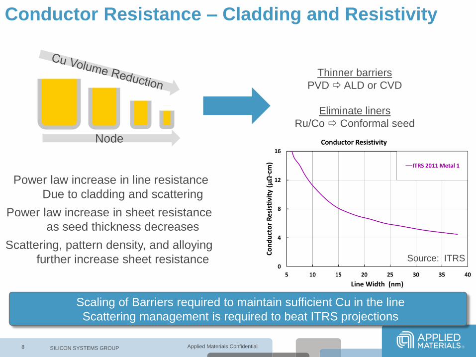
Conductor Resistance – Cladding and Resistivity
Thinner barriers
PVD ALD or CVD
Eliminate liners
Ru/Co Conformal seed
Scaling of Barriers required to maintain sufficient Cu in the line
Scattering management is required to beat ITRS projections
Power law increase in line resistance
Due to cladding and scattering
Power law increase in sheet resistance
as seed thickness decreases
Scattering, pattern density, and alloying
further increase sheet resistance
Node
Source: ITRS
Applied Materials Confidential
R 140
G 140
B 140
R 220
G 220
B 220
R 69
G 153
B 195
R 254
G 203
B 0
R 255
G 121
B 1
R 234
G 40
B 57
R 155
G 238
B 255
R 146
G 212
B 0
R 75
G 75
B 75
R 6
G 30
B 60
SILICON SYSTEMS GROUP
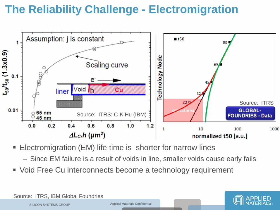
The Reliability Challenge - Electromigration
Electromigration (EM) life time is shorter for narrow lines
– Since EM failure is a result of voids in line, smaller voids cause early fails
Void Free Cu interconnects become a technology requirement
Source: ITRS, IBM Global Foundries
Source: ITRS: C-K Hu (IBM)
Source: ITRS
Applied Materials Confidential
R 140
G 140
B 140
R 220
G 220
B 220
R 69
G 153
B 195
R 254
G 203
B 0
R 255
G 121
B 1
R 234
G 40
B 57
R 155
G 238
B 255
R 146
G 212
B 0
R 75
G 75
B 75
R 6
G 30
B 60
SILICON SYSTEMS GROUP
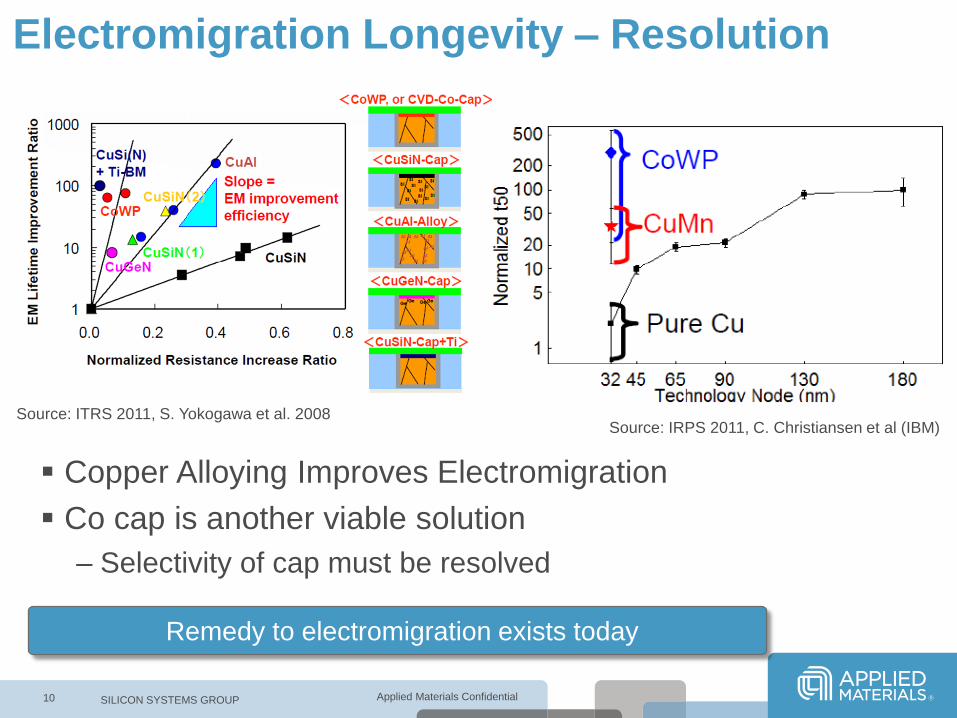
Electromigration Longevity – Resolution
10
Source: IRPS 2011, C. Christiansen et al (IBM)
Copper Alloying Improves Electromigration
Co cap is another viable solution
– Selectivity of cap must be resolved
Source: ITRS 2011, S. Yokogawa et al. 2008
Remedy to electromigration exists today
Applied Materials Confidential
R 140
G 140
B 140
R 220
G 220
B 220
R 69
G 153
B 195
R 254
G 203
B 0
R 255
G 121
B 1
R 234
G 40
B 57
R 155
G 238
B 255
R 146
G 212
B 0
R 75
G 75
B 75
R 6
G 30
B 60
SILICON SYSTEMS GROUP
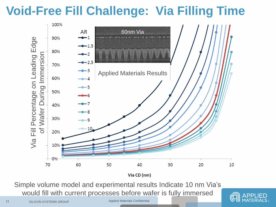
Void-Free Fill Challenge: Via Filling Time
11
0.59 seconds of plating
(2.94 Coulombs)
60nm Via
Simple volume model and experimental results Indicate 10 nm Via’s
would fill with current processes before wafer is fully immersed
Via
Fill
Perc
enta
ge o
n L
eadin
g E
dge
of
Wafe
r D
uring I
mm
ers
ion
Applied Materials Results
Applied Materials Confidential
R 140
G 140
B 140
R 220
G 220
B 220
R 69
G 153
B 195
R 254
G 203
B 0
R 255
G 121
B 1
R 234
G 40
B 57
R 155
G 238
B 255
R 146
G 212
B 0
R 75
G 75
B 75
R 6
G 30
B 60
SILICON SYSTEMS GROUP
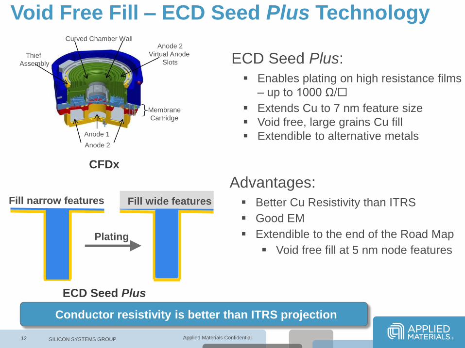
Fill narrow features Fill wide features
CFDx
ECD Seed Plus:
Enables plating on high resistance films
– up to 1000 Ω/
Extends Cu to 7 nm feature size
Void free, large grains Cu fill
Extendible to alternative metals
Plating
Conductor resistivity is better than ITRS projection
Void Free Fill – ECD Seed Plus Technology
Anode 2
Anode 1
Membrane
Cartridge
Anode 2
Virtual Anode
Slots
Curved Chamber Wall
Thief
Assembly
Advantages:
Better Cu Resistivity than ITRS
Good EM
Extendible to the end of the Road Map
Void free fill at 5 nm node features
12
ECD Seed Plus
Applied Materials Confidential
R 140
G 140
B 140
R 220
G 220
B 220
R 69
G 153
B 195
R 254
G 203
B 0
R 255
G 121
B 1
R 234
G 40
B 57
R 155
G 238
B 255
R 146
G 212
B 0
R 75
G 75
B 75
R 6
G 30
B 60
SILICON SYSTEMS GROUP
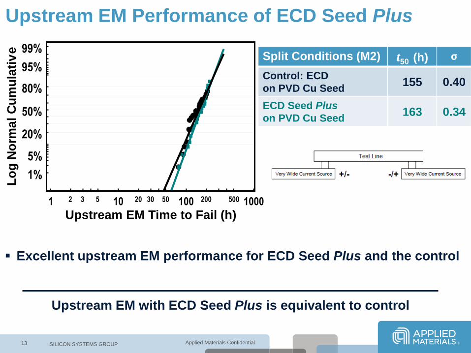
Upstream EM Performance of ECD Seed Plus
13
Split Conditions (M2) t50 (h) σ
Control: ECD
on PVD Cu Seed 155 0.40
ECD Seed Plus
on PVD Cu Seed 163 0.34
Excellent upstream EM performance for ECD Seed Plus and the control
Upstream EM with ECD Seed Plus is equivalent to control
50%
80%
20%
5%
1%
95%
99%
L o
g N
o r m
a l
C u
m u
l a t i
v e
1 10 5 3 2 100 50 30 20 1000 500 200
Upstream EM Time to Fail (h)
Applied Materials Confidential
R 140
G 140
B 140
R 220
G 220
B 220
R 69
G 153
B 195
R 254
G 203
B 0
R 255
G 121
B 1
R 234
G 40
B 57
R 155
G 238
B 255
R 146
G 212
B 0
R 75
G 75
B 75
R 6
G 30
B 60
SILICON SYSTEMS GROUP
Conductor resistivity is better than ITRS projection
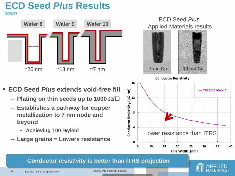
ECD Seed Plus Results 2/28/13
Wafer 8
~20 nm ~13 nm ~7 nm
Wafer 9 Wafer 10
7 nm Cu 10 nm Cu
No
rma
l P
rob
ab
ility
ECD Seed Plus
Applied Materials results
14
Lower resistance than ITRS
ECD Seed Plus extends void-free fill
– Plating on thin seeds up to 1000 W/
– Establishes a pathway for copper
metallization to 7 nm node and
beyond
• Achieving 100 %yield
– Large grains = Lowers resistance
Applied Materials Confidential
R 140
G 140
B 140
R 220
G 220
B 220
R 69
G 153
B 195
R 254
G 203
B 0
R 255
G 121
B 1
R 234
G 40
B 57
R 155
G 238
B 255
R 146
G 212
B 0
R 75
G 75
B 75
R 6
G 30
B 60
SILICON SYSTEMS GROUP
Conclusion and Summary
Scaling poses major challenges to Interconnect Integration
– Defects, Cladding, Reliability, Void-Free, High Sheet Resistance, Resistance
– Will Cu extend or will there be a paradigm change?
• We present a pathway to extending Cu to the end of the road map
Doped or caped Cu resolve the electromigration challenge
Barrier evolution resolves the cladding challenge
ECD Seed Plus extends void-free fill to the end of the road map
– Plating on thin seeds up to 1000 W/
– Establishes a pathway for copper metallization to 7 nm node and beyond
– Widens the process window for high aspect ratios
– Lowers resistance due to larger grain growth
– Good interconnect reliability
Thanks you
15
Interconnect metallization extends