Interconnections: Aluminum Metallization - … Aluminum Metallization Advances in the multilevel...
25
EE 311 /Prof Saraswat Spring 2003 Interconnections: Aluminum Metallization Advances in the multilevel interconnect technology 70’s Poly-Si Aluminum 80’s Local planarization Aluminum alloys Silicide contacts Polycide gates 90’s Global planarization Salicides CVD tungsten plugs Low K dielectrics last and present decades: Copper Low k dielectrics
-
Upload
nguyenkhanh -
Category
Documents
-
view
226 -
download
0
Transcript of Interconnections: Aluminum Metallization - … Aluminum Metallization Advances in the multilevel...
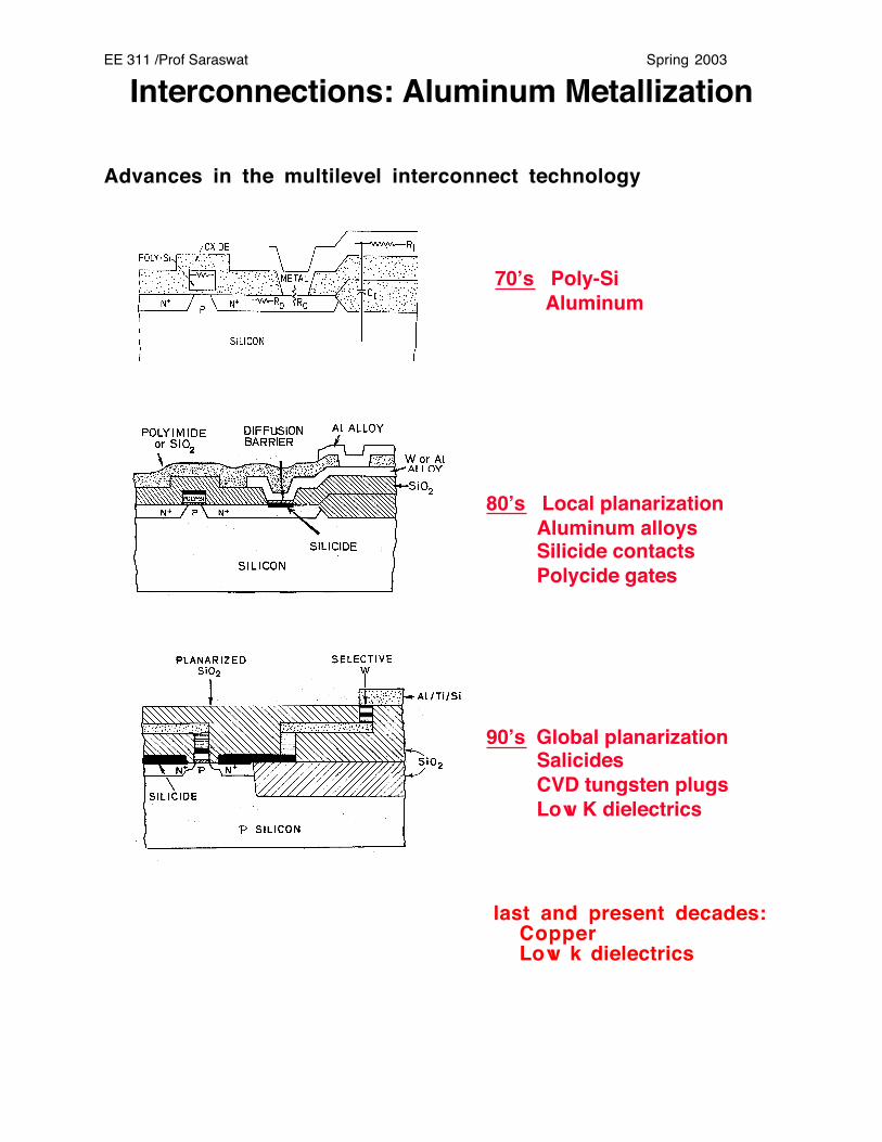
EE 311 /Prof Saraswat Spring 2003
Interconnections: Aluminum Metallization
Advances in the multilevel interconnect technology
70’s Poly-SiAluminum
80’s Local planarizationAluminum alloysSilicide contactsPolycide gates
90’s Global planarizationSalicidesCVD tungsten plugsLow K dielectrics
last and present decades:CopperLow k dielectrics
EE 311 /Prof Saraswat Al Interconnect
2
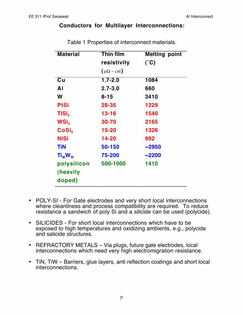
Conductors for Multilayer Interconnections:
Table 1 Properties of interconnect materials.
Material Thin filmresistivity(µΩ − cm)
Melting point(˚C)
Cu 1.7-2.0 1084Al 2.7-3.0 660W 8-15 3410PtSi 28-35 1229TiSi2 13-16 1540WSi2 30-70 2165CoSi2 15-20 1326NiSi 14-20 992TiN 50-150 ~2950Ti30W70 75-200 ~2200polysilicon(heavilydoped)
500-1000 1410
• POLY-SI - For Gate electrodes and very short local interconnectionswhere cleanliness and process compatibility are required. To reduceresistance a sandwich of poly Si and a silicide can be used (polycide).
• SILICIDES - For short local interconnections which have to beexposed to high temperatures and oxidizing ambients, e.g., polycideand salicide structures.
• REFRACTORY METALS – Via plugs, future gate electrodes, localinterconnections which need very high electromigration resistance.
• TiN, TiW – Barriers, glue layers, anti reflection coatings and short localinterconnections.
EE 311 /Prof Saraswat Al Interconnect
3
ALUMINUM and COPPER - For those layers where low resistivity isrequired, i.e., global and semi global interconnections.
• Al has been used widely in the past and is still used− Low resistivity− Ease of deposition,− Dry etching− Does not contaminate Si− Ohmic contacts to Si but problem with shallow junctions− Excellent adhesion to dielectrics− Problems with Al
• Electromigration=> lower life time• Hillocks=> shorts between levels
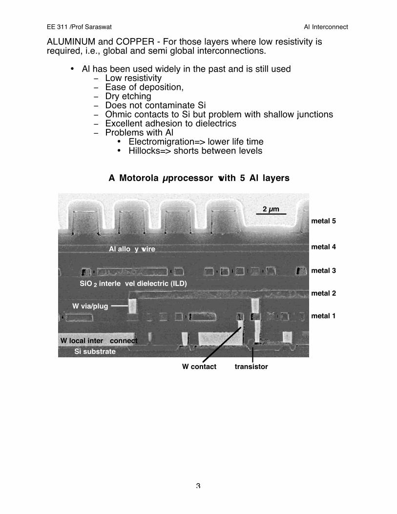
A Motorola µprocessor with 5 Al layers
Al allo y wire
SiO 2 interle vel dielectric (ILD)
W via/plug
transistor
W local inter connect
metal 1
metal 2
metal 3
metal 4
metal 5
Si substrate
2 µm
W contact
EE 311 /Prof Saraswat Al Interconnect
4
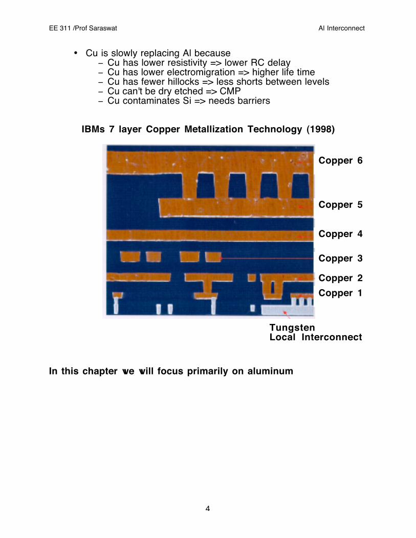
• Cu is slowly replacing Al because− Cu has lower resistivity => lower RC delay− Cu has lower electromigration => higher life time− Cu has fewer hillocks => less shorts between levels− Cu can't be dry etched => CMP− Cu contaminates Si => needs barriers
IBMs 7 layer Copper Metallization Technology (1998)
In this chapter we will focus primarily on aluminum
Copper 6
Copper 1
TungstenLocal Interconnect
Copper 3
Copper 5
Copper 4
Copper 2
EE 311 /Prof Saraswat Al Interconnect
5
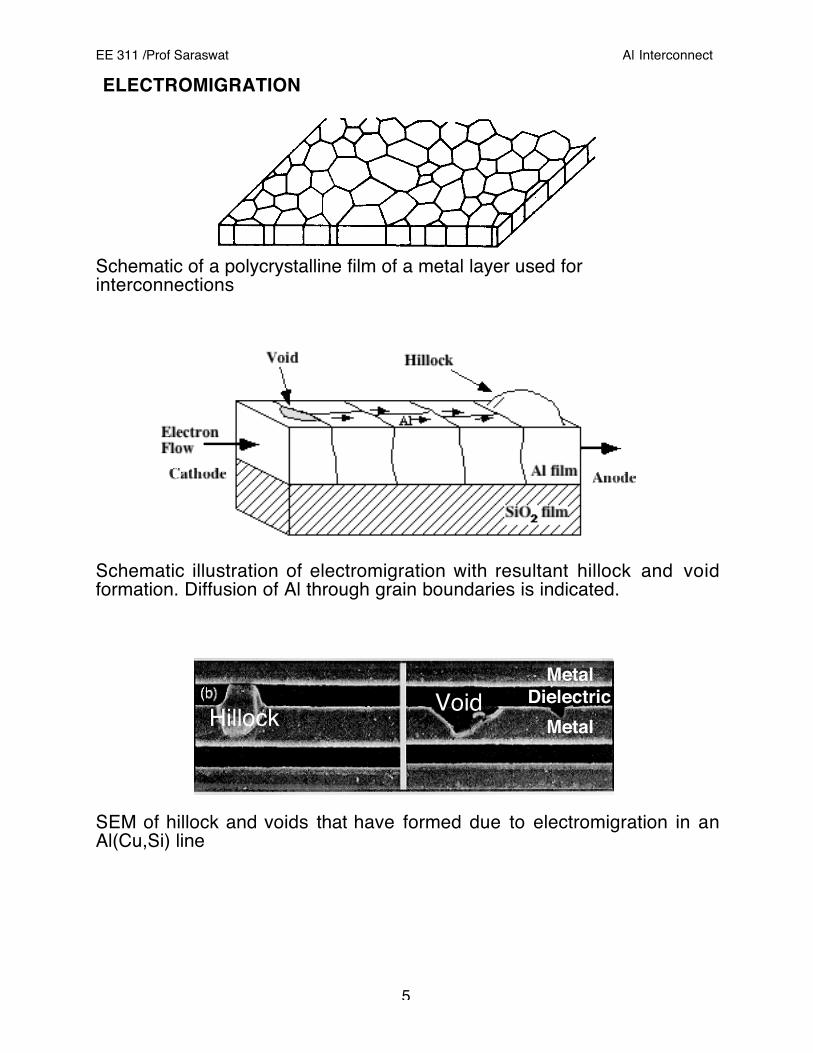
ELECTROMIGRATION
Schematic of a polycrystalline film of a metal layer used forinterconnections
Schematic illustration of electromigration with resultant hillock and voidformation. Diffusion of Al through grain boundaries is indicated.
voidHillock Void
Metal
MetalDielectric
SEM of hillock and voids that have formed due to electromigration in anAl(Cu,Si) line
EE 311 /Prof Saraswat Al Interconnect
6
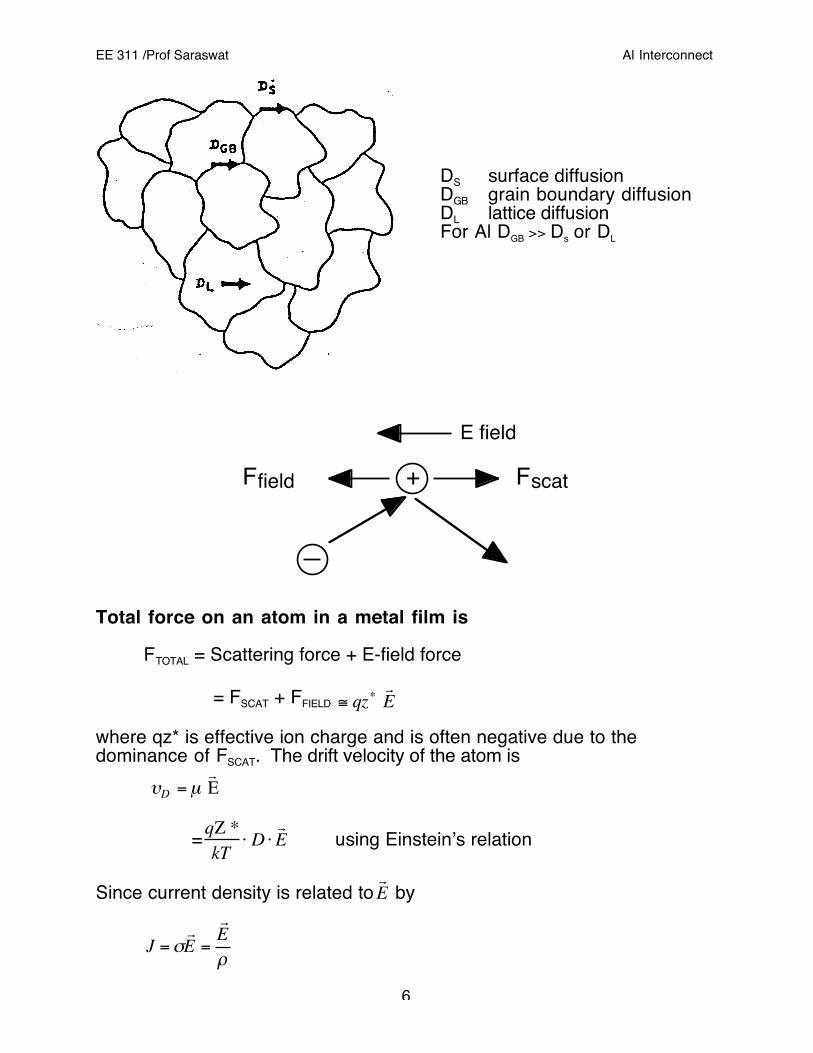
FscatFfield +
E field
Total force on an atom in a metal film is
FTOTAL = Scattering force + E-field force
= FSCAT + FFIELD
€
≅ qz∗r E
where qz* is effective ion charge and is often negative due to thedominance of FSCAT. The drift velocity of the atom is
€
υD = µr Ε
=
qΖ *kT
⋅ D ⋅r E using Einstein’s relation
Since current density is related to r E by
€
J =σr E =
r E ρ
DS surface diffusionDGB grain boundary diffusionDL lattice diffusionFor Al DGB >> Ds or DL
EE 311 /Prof Saraswat Al Interconnect
7
And diffusivity is in general given by
D = Do e−kTEa
€
υD = J ρ qZ *kT
D0 e−Ea
kT
Meantime to failure (MTF) is thus
MTF ∝ e EakT
A phenomenological model for MTF is
MTF = A
γ m JneEa kT
Where A is a materials related factor, γ is the duty factor, m and n areconstants and T is the operation temperature. Constant n is generallybetween 1 and 3
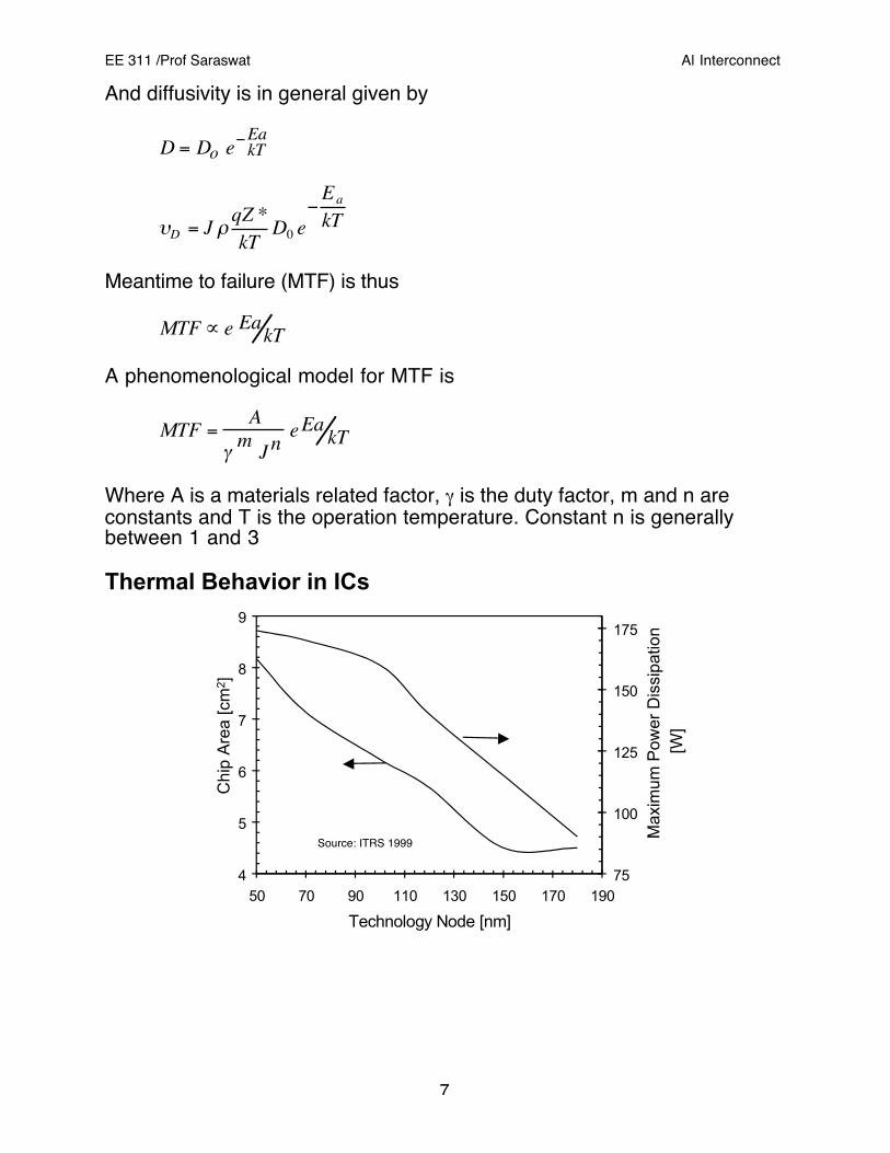
Thermal Behavior in ICs
4
5
6
7
8
9
50 70 90 110 130 150 170 190
Technology Node [nm]
Chi
p A
rea
[cm
2 ]
75
100
125
150
175
Max
imum
Pow
er D
issi
patio
n [W
]
Source: ITRS 1999
EE 311 /Prof Saraswat Al Interconnect
8
• In addition to the power dissipated by devices there is power dissipationdue to interconnects:
• Joule heating due to I2R loss• Energy dissipated (CV2f) is increasing as performance improves
Average chip and interconnect temperature is rising
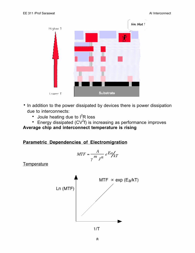
Parametric Dependencies of Electromigration
MTF = A
γ m JneEa kT
Temperature
EE 311 /Prof Saraswat Al Interconnect
9
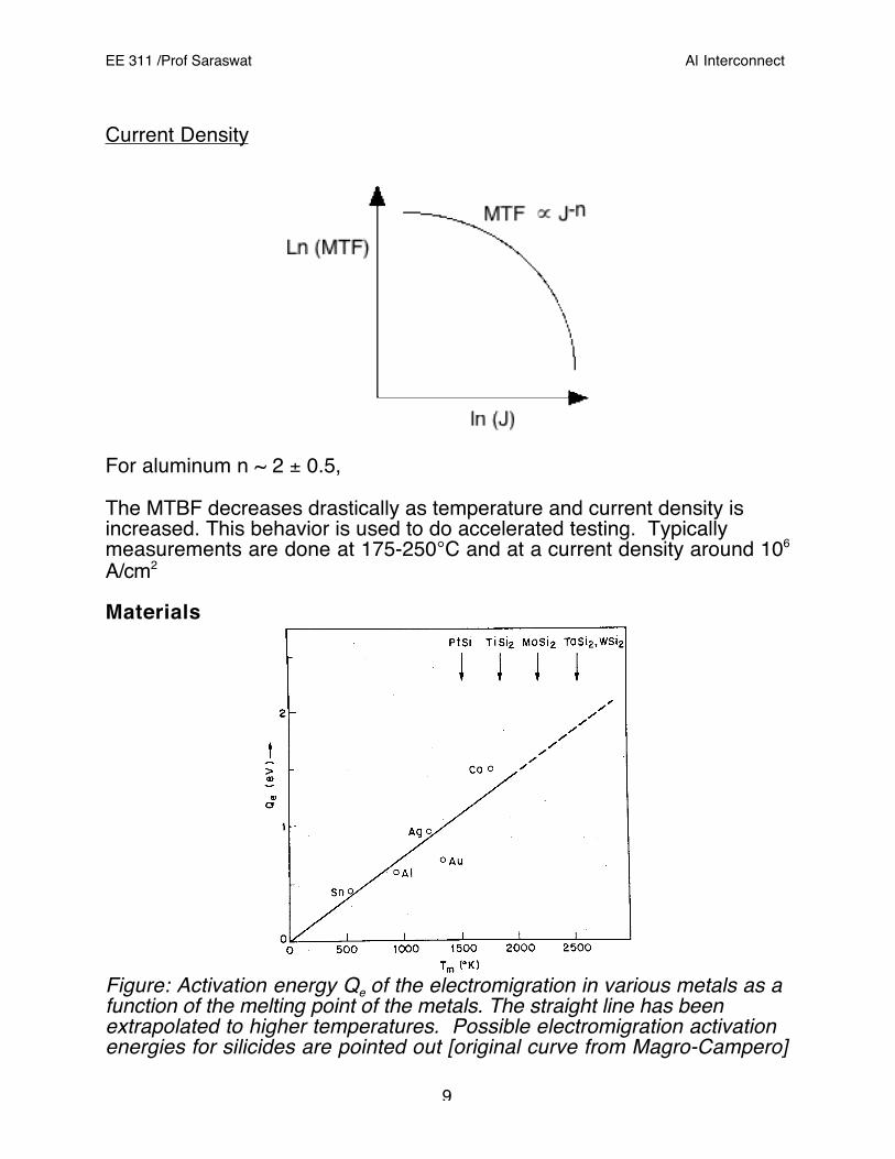
Current Density
For aluminum n ~ 2 ± 0.5,
The MTBF decreases drastically as temperature and current density isincreased. This behavior is used to do accelerated testing. Typicallymeasurements are done at 175-250°C and at a current density around 106
A/cm2
Materials
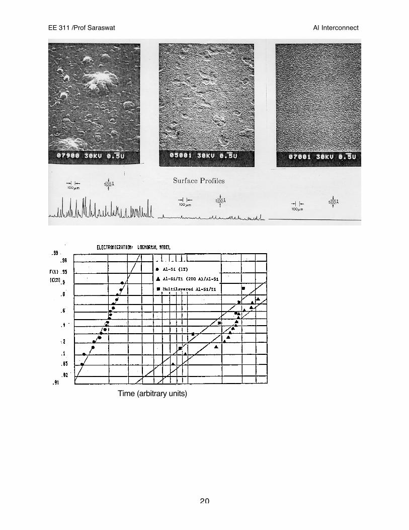
Figure: Activation energy Qe of the electromigration in various metals as afunction of the melting point of the metals. The straight line has beenextrapolated to higher temperatures. Possible electromigration activationenergies for silicides are pointed out [original curve from Magro-Campero]
EE 311 /Prof Saraswat Al Interconnect
10
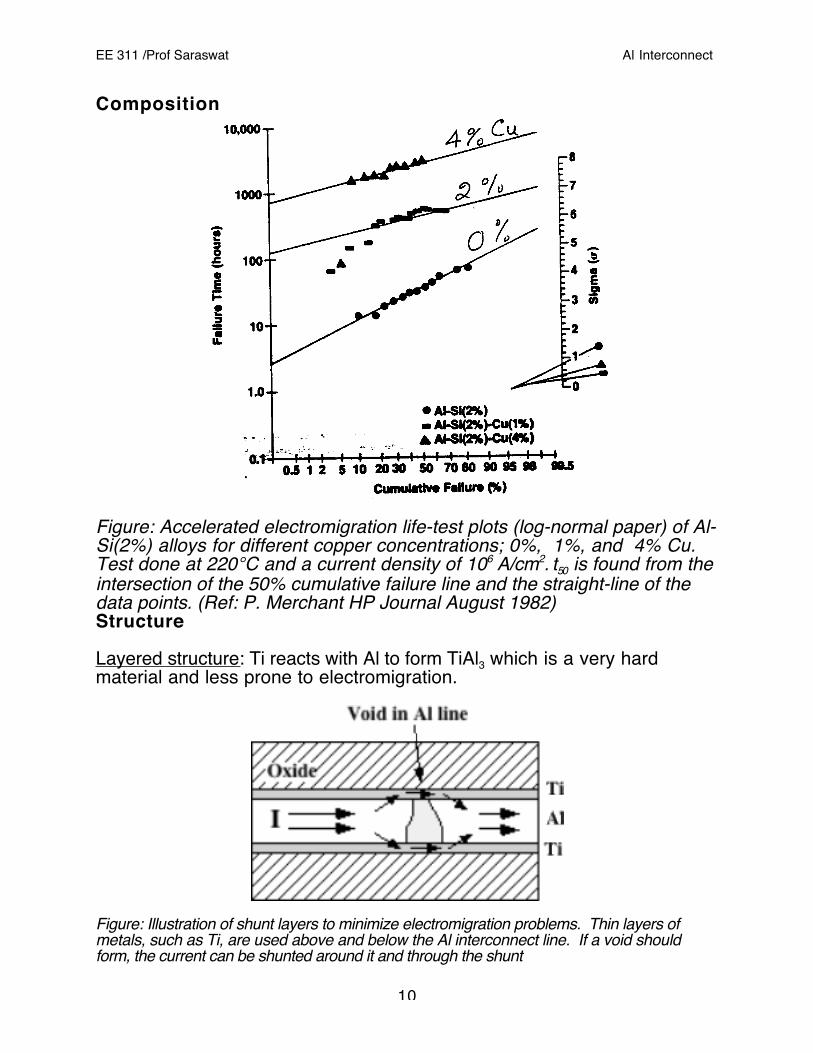
Composition
Figure: Accelerated electromigration life-test plots (log-normal paper) of Al-Si(2%) alloys for different copper concentrations; 0%, 1%, and 4% Cu.Test done at 220°C and a current density of 106 A/cm2. t50 is found from theintersection of the 50% cumulative failure line and the straight-line of thedata points. (Ref: P. Merchant HP Journal August 1982)Structure
Layered structure: Ti reacts with Al to form TiAl3 which is a very hardmaterial and less prone to electromigration.
Figure: Illustration of shunt layers to minimize electromigration problems. Thin layers ofmetals, such as Ti, are used above and below the Al interconnect line. If a void shouldform, the current can be shunted around it and through the shunt
EE 311 /Prof Saraswat Al Interconnect
11
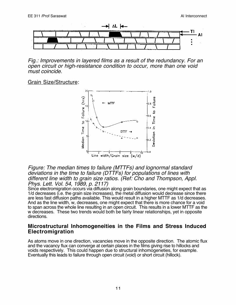
Fig.: Improvements in layered films as a result of the redundancy. For anopen circuit or high-resistance condition to occur, more than one voidmust coincide.
Grain Size/Structure:
Figure: The median times to failure (MTTFs) and lognormal standarddeviations in the time to failure (DTTFs) for populations of lines withdifferent line width to grain size ratios. (Ref: Cho and Thompson, Appl.Phys. Lett. Vol. 54, 1989, p. 2117)Since electromigration occurs via diffusion along grain boundaries, one might expect that as1/d decreases (i.e. the grain size increases), the metal diffusion would decrease since thereare less fast diffusion paths available. This would result in a higher MTTF as 1/d decreases.And as the line width, w, decreases, one might expect that there is more chance for a voidto span across the whole line resulting in an open circuit. This results in a lower MTTF as thew decreases. These two trends would both be fairly linear relationships, yet in oppositedirections.
Microstructural Inhomogeneities in the Films and Stress InducedElectromigrationAs atoms move in one direction, vacancies move in the opposite direction. The atomic fluxand the vacancy flux can converge at certain places in the films giving rise to hillocks andvoids respectively. This could happen due to structural inhomogeneties, for example.Eventually this leads to failure through open circuit (void) or short circuit (hillock).
EE 311 /Prof Saraswat Al Interconnect
12
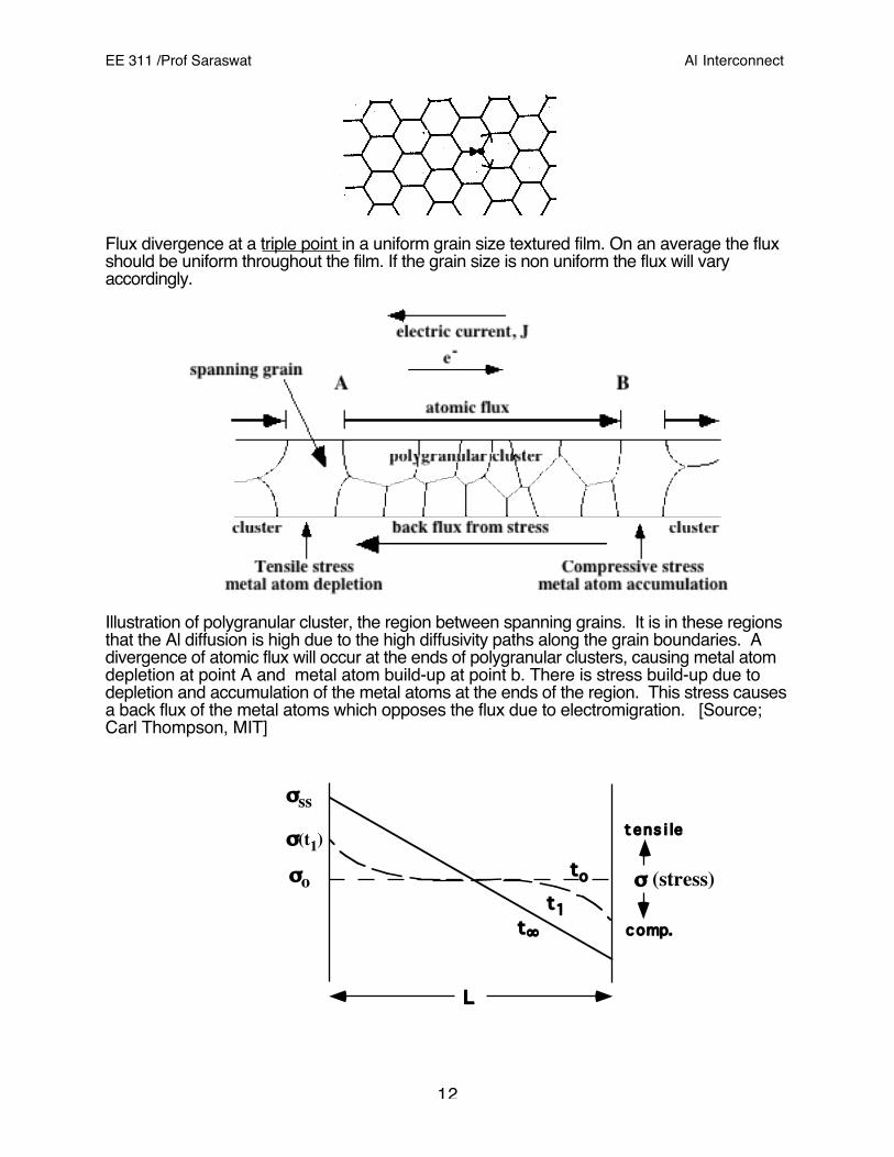
Flux divergence at a triple point in a uniform grain size textured film. On an average the fluxshould be uniform throughout the film. If the grain size is non uniform the flux will varyaccordingly.
Illustration of polygranular cluster, the region between spanning grains. It is in these regionsthat the Al diffusion is high due to the high diffusivity paths along the grain boundaries. Adivergence of atomic flux will occur at the ends of polygranular clusters, causing metal atomdepletion at point A and metal atom build-up at point b. There is stress build-up due todepletion and accumulation of the metal atoms at the ends of the region. This stress causesa back flux of the metal atoms which opposes the flux due to electromigration. [Source;Carl Thompson, MIT]
e-
σ (stress)tot1
t∞
σss
σo
σ(t1)
L
comp.
t ens i le
EE 311 /Prof Saraswat Al Interconnect
13
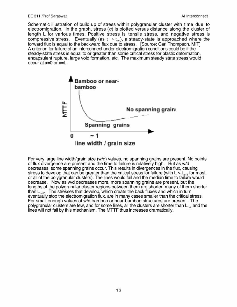
Schematic illustration of build up of stress within polygranular cluster with time due toelectromigration. In the graph, stress (σ) is plotted versus distance along the cluster oflength L for various times. Positive stress is tensile stress, and negative stress iscompressive stress. Eventually (as t → t∞ ), a steady-state is approached where theforward flux is equal to the backward flux due to stress. [Source; Carl Thompson, MIT]A criterion for failure of an interconnect under electromigration conditions could be if thesteady-state stress is equal to or greater than some critical stress for plastic deformation,encapsulent rupture, large void formation, etc. The maximum steady state stress wouldoccur at x=0 or x=L
For very large line width/grain size (w/d) values, no spanning grains are present. No pointsof flux divergence are present and the time to failure is relatively high. But as w/ddecreases, some spanning grains occur. This results in divergences in the flux, causingstress to develop that can be greater than the critical stress for failure (with L > Lcrit for mostor all of the polygranular clusters). The lines would fail and the median time to failure woulddecrease. Now as w/d decreases more, more spanning grains are present, but thelengths of the polygranular cluster regions between them are shorter, many of them shorterthan Lcrit. The stresses that develop, which create the back fluxes and which in turneventually stop the electromigration flux, are in many cases smaller than the critical stress.For small enough values of w/d bamboo or near-bamboo structures are present. Thepolygranular clusters are few, and for some lines, all the clusters are shorter than Lcrit and thelines will not fail by this mechanism. The MTTF thus increases dramatically.
EE 311 /Prof Saraswat Al Interconnect
14
(a)
(b)
(c)
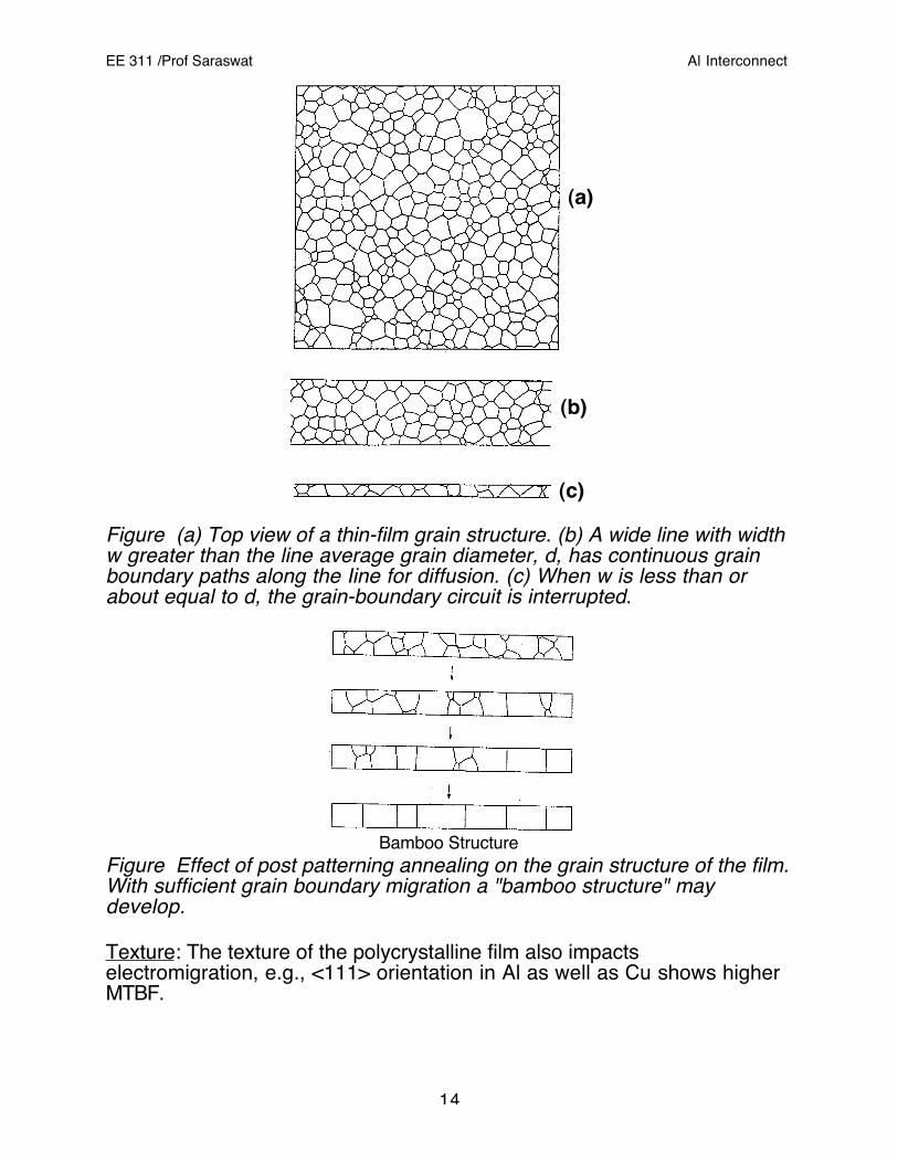
Figure (a) Top view of a thin-film grain structure. (b) A wide line with widthw greater than the line average grain diameter, d, has continuous grainboundary paths along the Iine for diffusion. (c) When w is less than orabout equal to d, the grain-boundary circuit is interrupted.
Bamboo StructureFigure Effect of post patterning annealing on the grain structure of the film.With sufficient grain boundary migration a "bamboo structure" maydevelop.
Texture: The texture of the polycrystalline film also impactselectromigration, e.g., <111> orientation in Al as well as Cu shows higherMTBF.
EE 311 /Prof Saraswat Al Interconnect
15
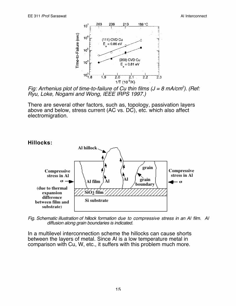
Fig: Arrhenius plot of time-to-failure of Cu thin films (J = 8 mA/cm2). (Ref:Ryu, Loke, Nogami and Wong, IEEE IRPS 1997.)
There are several other factors, such as, topology, passivation layersabove and below, stress current (AC vs. DC), etc. which also affectelectromigration.
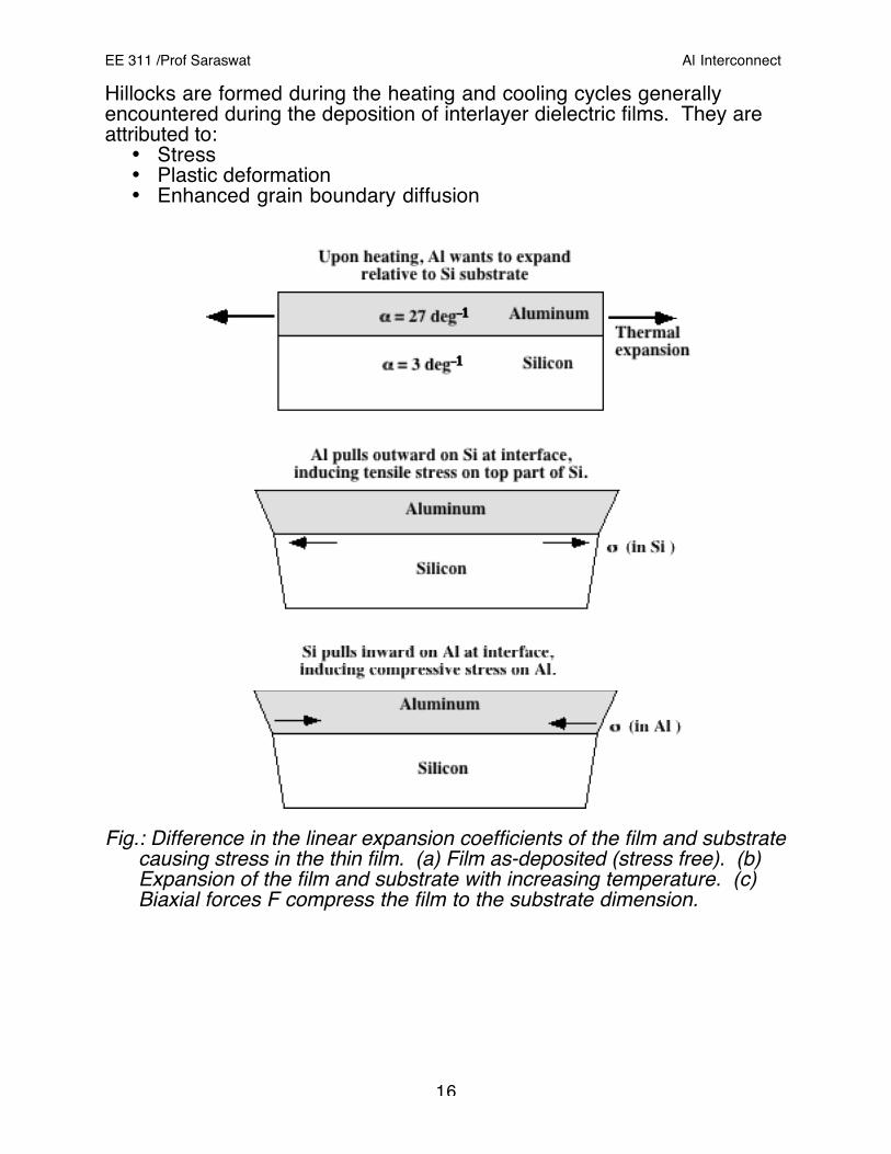
Hillocks:
Fig. Schematic illustration of hillock formation due to compressive stress in an Al film. Aldiffusion along grain boundaries is indicated.
In a multilevel interconnection scheme the hillocks can cause shortsbetween the layers of metal. Since Al is a low temperature metal incomparison with Cu, W, etc., it suffers with this problem much more.
EE 311 /Prof Saraswat Al Interconnect
16
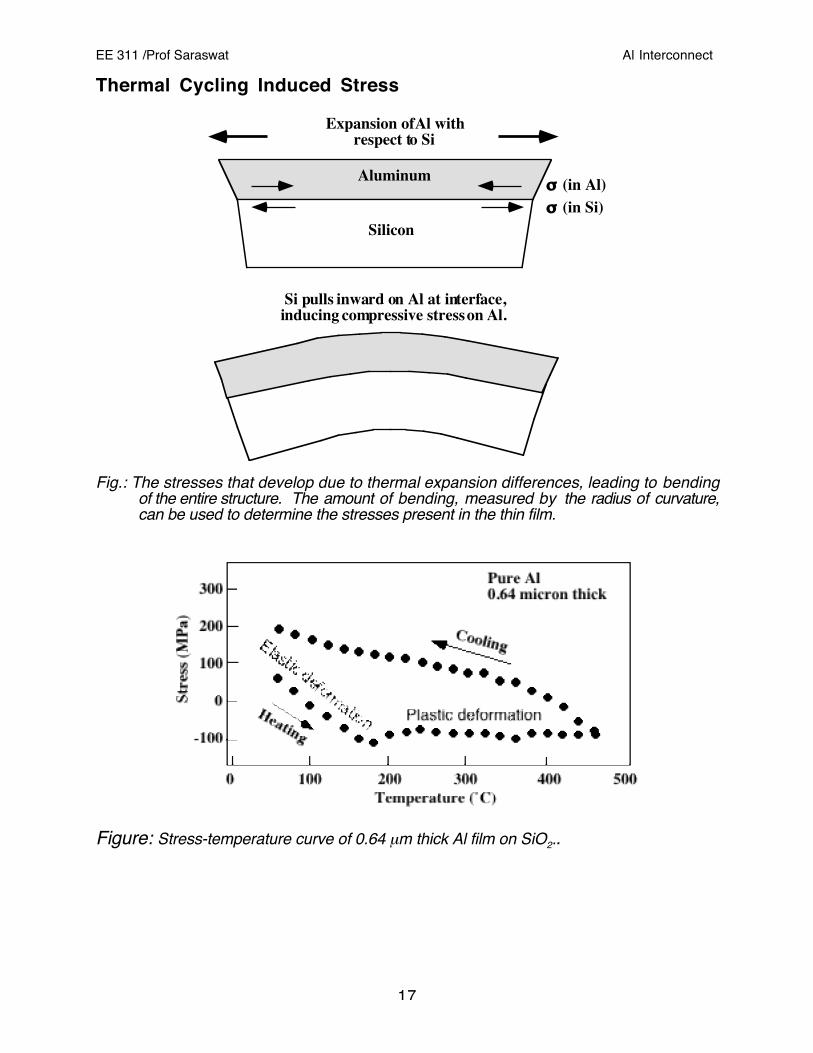
Hillocks are formed during the heating and cooling cycles generallyencountered during the deposition of interlayer dielectric films. They areattributed to:
• Stress• Plastic deformation• Enhanced grain boundary diffusion
Fig.: Difference in the linear expansion coefficients of the film and substratecausing stress in the thin film. (a) Film as-deposited (stress free). (b)Expansion of the film and substrate with increasing temperature. (c)Biaxial forces F compress the film to the substrate dimension.
EE 311 /Prof Saraswat Al Interconnect
17
Thermal Cycling Induced Stress
Silicon
Aluminum
σ (in Si)
Si pulls inward on Al at interface,inducing compressive stress on Al.
σ (in Al)
Expansion of Al withrespect to Si
Fig.: The stresses that develop due to thermal expansion differences, leading to bendingof the entire structure. The amount of bending, measured by the radius of curvature,can be used to determine the stresses present in the thin film.
Figure: Stress-temperature curve of 0.64 µm thick Al film on SiO2..
EE 311 /Prof Saraswat Al Interconnect
18
LASER
rotating mirror
lens
film on wafer
Photodetector
Furnace
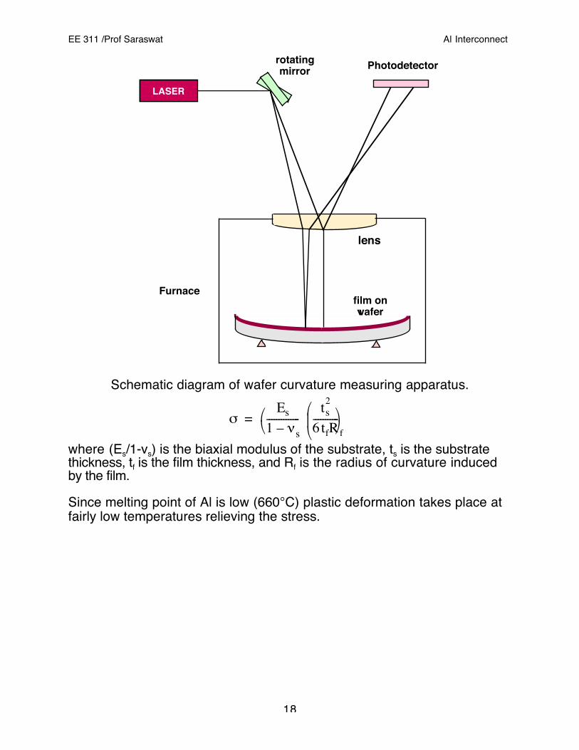
Schematic diagram of wafer curvature measuring apparatus.
σEs
1 νs–-------------- ts
2
6 tfR-----------
f
=
where (Es/1-vs) is the biaxial modulus of the substrate, ts is the substratethickness, tf is the film thickness, and Rf is the radius of curvature inducedby the film.
Since melting point of Al is low (660°C) plastic deformation takes place atfairly low temperatures relieving the stress.
EE 311 /Prof Saraswat Al Interconnect
19
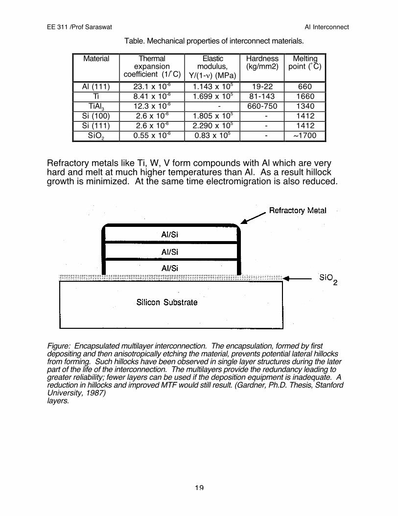
Table. Mechanical properties of interconnect materials.
Material Thermalexpansion
coefficient (1/˚C)
Elasticmodulus,
Y/(1-ν) (MPa)
Hardness(kg/mm2)
Meltingpoint (˚C)
Al (111) 23.1 x 10⁻⁶ 1.143 x 10⁵ 19-22 660Ti 8.41 x 10⁻⁶ 1.699 x 10⁵ 81-143 1660
TiAl3 12.3 x 10⁻⁶ - 660-750 1340Si (100) 2.6 x 10⁻⁶ 1.805 x 10⁵ - 1412Si (111) 2.6 x 10⁻⁶ 2.290 x 10⁵ - 1412
SiO2 0.55 x 10⁻⁶ 0.83 x 10⁵ - ~1700
Refractory metals like Ti, W, V form compounds with Al which are veryhard and melt at much higher temperatures than Al. As a result hillockgrowth is minimized. At the same time electromigration is also reduced.
Figure: Encapsulated multilayer interconnection. The encapsulation, formed by firstdepositing and then anisotropically etching the material, prevents potential lateral hillocksfrom forming. Such hillocks have been observed in single layer structures during the laterpart of the life of the interconnection. The multilayers provide the redundancy leading togreater reliability; fewer layers can be used if the deposition equipment is inadequate. Areduction in hillocks and improved MTF would still result. (Gardner, Ph.D. Thesis, StanfordUniversity, 1987)layers.
EE 311 /Prof Saraswat Al Interconnect
20
Time (arbitrary units)
EE 311 /Prof Saraswat Al Interconnect
21
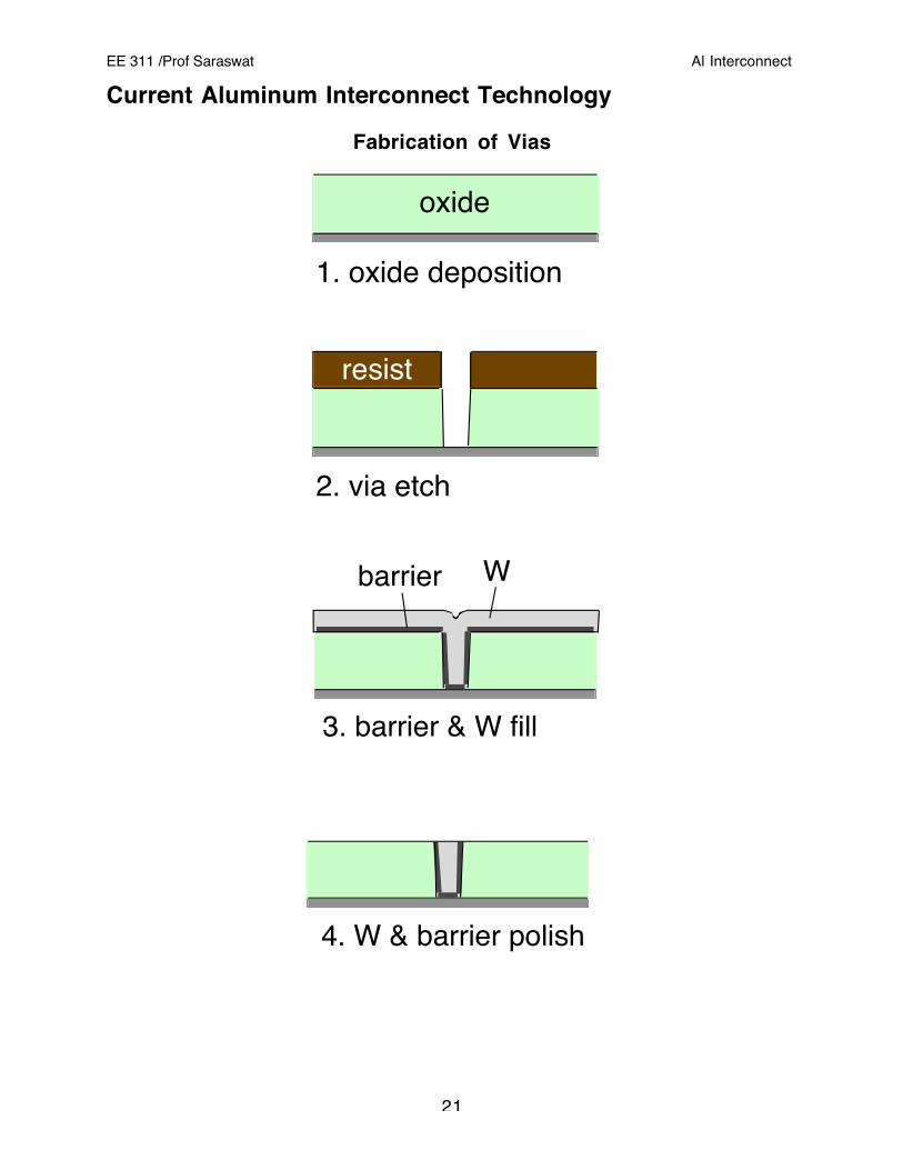
Current Aluminum Interconnect Technology
Fabrication of Vias
oxide
1. oxide deposition
2. via etch
resist
barrier W
4. W & barrier polish
3. barrier & W fill
EE 311 /Prof Saraswat Al Interconnect
22
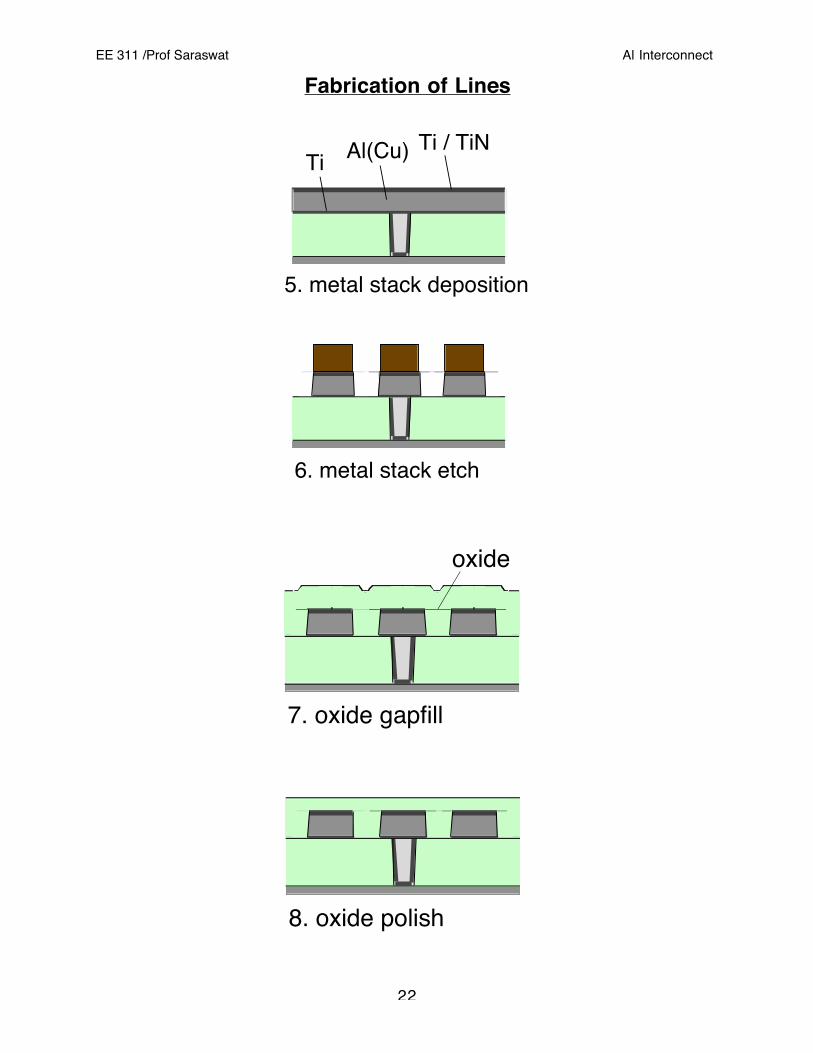
Fabrication of Lines
Ti / TiNAl(Cu)Ti
5. metal stack deposition
6. metal stack etch
8. oxide polish
7. oxide gapfill
oxide
EE 311 /Prof Saraswat Al Interconnect
23
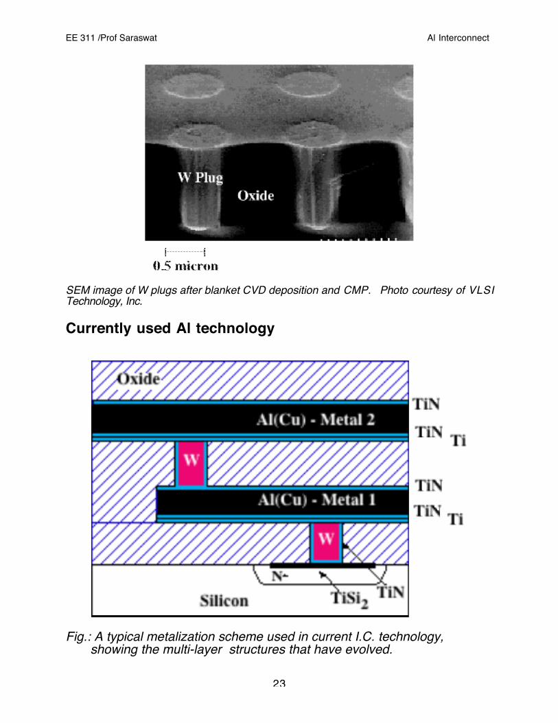
SEM image of W plugs after blanket CVD deposition and CMP. Photo courtesy of VLSITechnology, Inc.
Currently used Al technology
Fig.: A typical metalization scheme used in current I.C. technology,showing the multi-layer structures that have evolved.
EE 311 /Prof Saraswat Al Interconnect
24
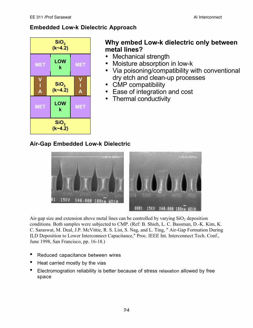
Embedded Low-k Dielectric Approach
VIA
VIA
METMETLOWk
METMETLOWk
SiO2(k~4.2)
SiO2(k~4.2)
SiO2(k~4.2)
Air-Gap Embedded Low-k Dielectric
1µm
L/S=0.30µm L/S=0.30µm
Air-gap size and extension above metal lines can be controlled by varying SiO2 depositionconditions. Both samples were subjected to CMP. (Ref: B. Shieh, L. C. Bassman, D.-K. Kim, K.C. Saraswat, M. Deal, J.P. McVittie, R. S. List, S. Nag, and L. Ting, " Air-Gap Formation DuringILD Deposition to Lower Interconnect Capacitance," Proc. IEEE Int. Interconnect Tech. Conf.,June 1998, San Francisco, pp. 16-18.)
• Reduced capacitance between wires
• Heat carried mostly by the vias
• Electromogration reliability is better because of stress relaxation allowed by freespace
Why embed Low-k dielectric only betweenmetal lines?• Mechanical strength• Moisture absorption in low-k• Via poisoning/compatibility with conventional
dry etch and clean-up processes• CMP compatibility• Ease of integration and cost• Thermal conductivity
EE 311 /Prof Saraswat Al Interconnect
25
2.0
2.5
3.0
3.5
4.0
4.5
0.2 0.4 0.6 0.8 1Line/Space (um)
Kef
f
Experimental
Simulated
Keff vs. Feature Size
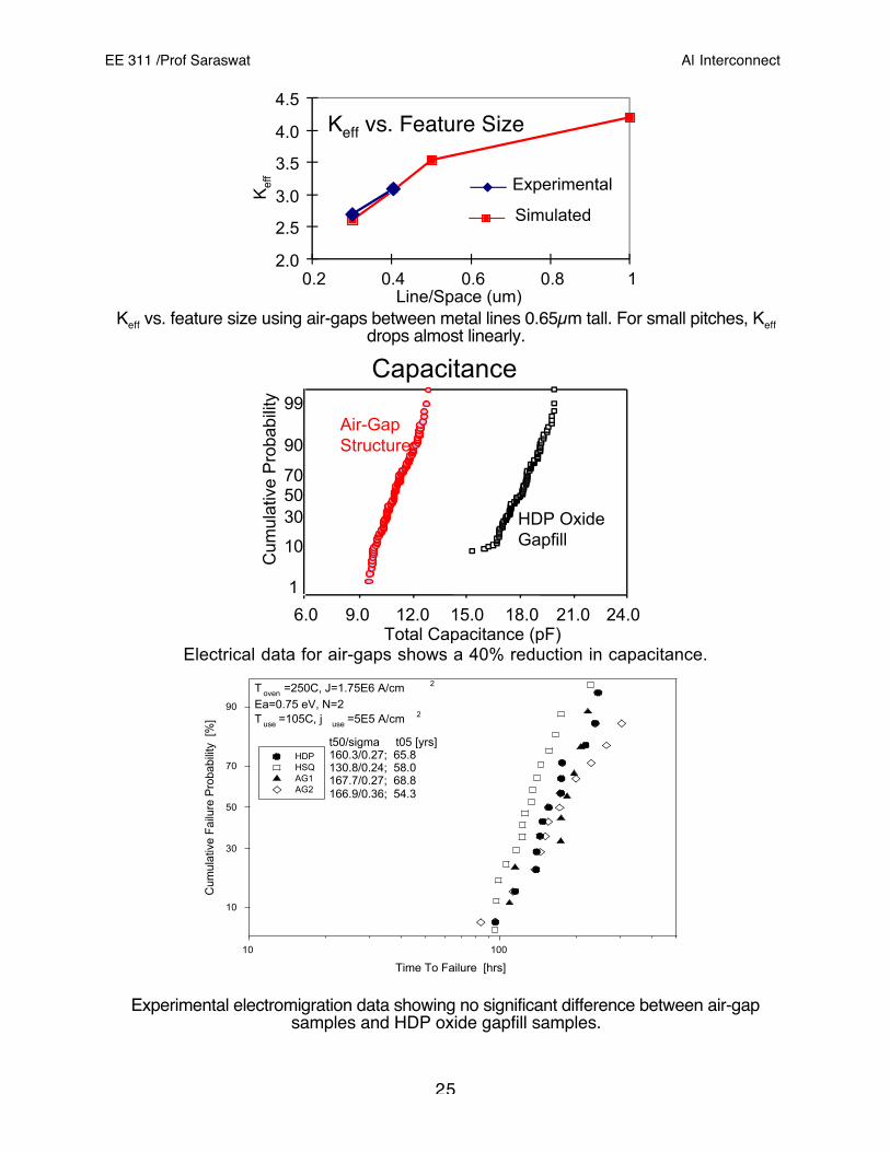
Keff vs. feature size using air-gaps between metal lines 0.65µm tall. For small pitches, Keffdrops almost linearly.
Capacitance
Total Capacitance (pF)6.0 9.0 12.0 15.0 18.0 21.0 24.0
1
10
305070
90
99Air-GapStructure
HDP OxideGapfill
Cum
ulat
ive
Pro
babi
lity
Electrical data for air-gaps shows a 40% reduction in capacitance.Bow-Tie Lead EM (CMP2, W=10um)
Time To Failure [hrs]
10 100
Cum
ulat
ive
Fai
lure
Pro
babi
lity
[%]
10
30
50
70
90
HDPHSQAG1AG2
t50/sigma t05 [yrs]160.3/0.27; 65.8130.8/0.24; 58.0167.7/0.27; 68.8166.9/0.36; 54.3
T oven =250C, J=1.75E6 A/cm 2
Ea=0.75 eV, N=2T use =105C, j use =5E5 A/cm 2
Experimental electromigration data showing no significant difference between air-gapsamples and HDP oxide gapfill samples.