Inside the Box: A New Hope for Optics? - RLE at MIT Institute of Technology Inside the Box: A New...
16
Integrated Systems Group Massachusetts Institute of Technology Inside the Box: A New Hope for Optics? Vladimir Stojanović
Transcript of Inside the Box: A New Hope for Optics? - RLE at MIT Institute of Technology Inside the Box: A New...

Integrated Systems GroupMassachusetts Institute of Technology
Inside the Box: A New Hope for Optics?
Vladimir Stojanović
Integrated Systems Group 2
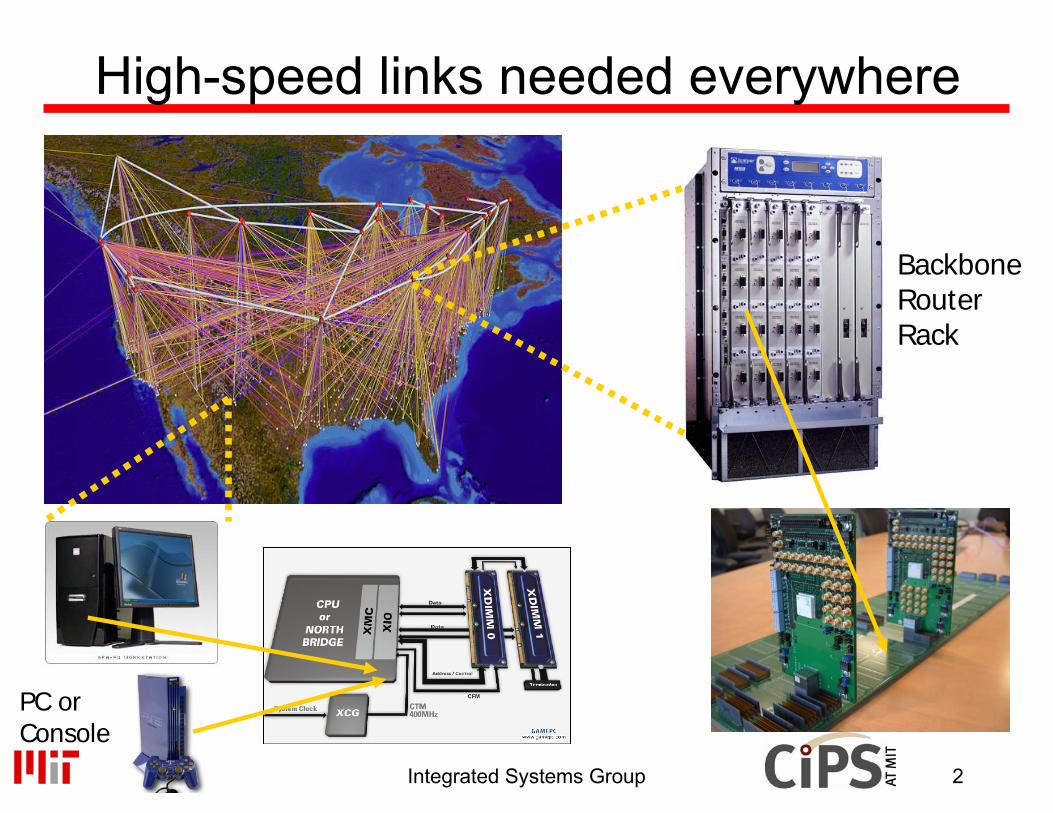
High-speed links needed everywhere
Backbone Router Rack
PC or Console
Integrated Systems Group 3
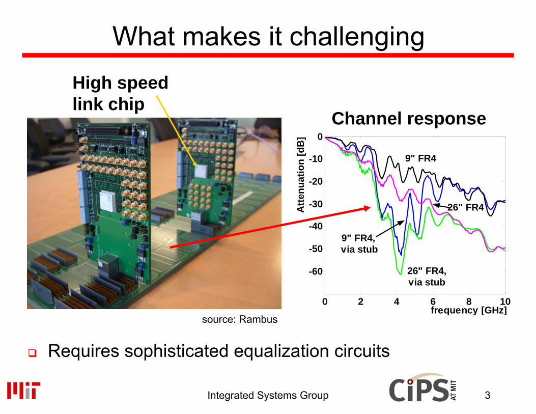
What makes it challenging
Requires sophisticated equalization circuits
High speed link chip
source: Rambus
0 2 4 6 8 10
-60
-50
-40
-30
-20
-10
0
frequency [GHz]A
ttenu
atio
n [d
B]
9" FR4, via stub
26" FR4,via stub
26" FR4
9" FR4
Channel response

Integrated Systems Group 4
Chip-to-chip I/O scaling problem
Bandwidth need grows faster than energy/bit dropsCreates exponentially increasing I/O power consumption
In power constrained systems (like processors and anything inside the box) – this limits the available bandwidth
9078
6859
5245
4036
3228
2522
2018
1614
y = 10800x-2.1
1
10
100
10 100
#I/O padsOff-chip fclkAggr BWAggr BW (Fit)
Technology (nm)N
orm
aliz
ed u
nit t
o 90
nm n
ode
9078
6859
5245
4036
3228
2522
2018
1614
y = 10800x-2.1
1
10
100
10 100
#I/O padsOff-chip fclkAggr BWAggr BW (Fit)
Technology (nm)N
orm
aliz
ed u
nit t
o 90
nm n
ode
y = 399.17x1.157
1
10
100
1000
0.01 0.1 1
Erg/bit (2-PAM)
Erg/bit Trend (2-PAM)
Technology (μm)
Ene
rgy/
bit (
pJ)
y = 399.17x1.157
1
10
100
1000
0.01 0.1 1
Erg/bit (2-PAM)
Erg/bit Trend (2-PAM)
Technology (μm)
Ene
rgy/
bit (
pJ)
[Ken Yang, UCLA]
Integrated Systems Group 5
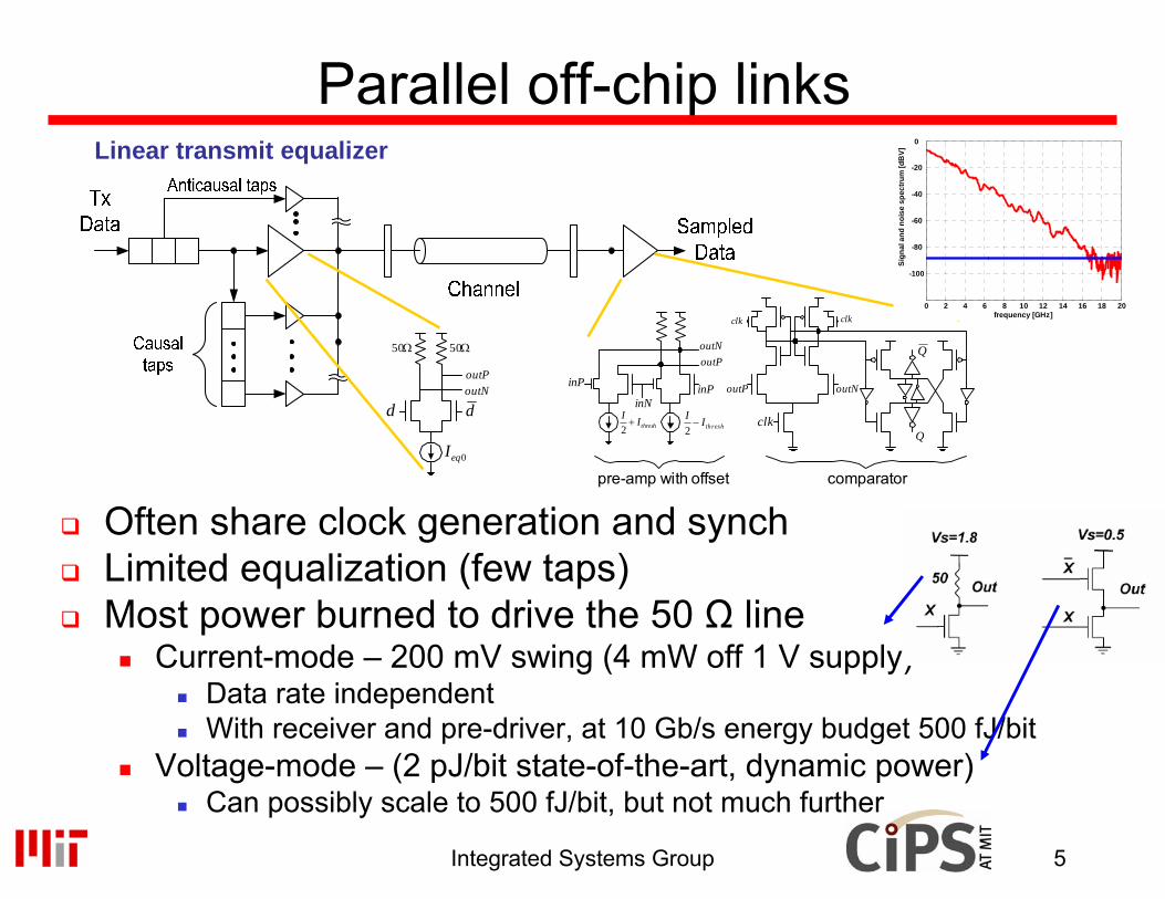
Parallel off-chip links
Often share clock generation and synchLimited equalization (few taps)Most power burned to drive the 50 Ω line
Current-mode – 200 mV swing (4 mW off 1 V supply)Data rate independentWith receiver and pre-driver, at 10 Gb/s energy budget 500 fJ/bit
Voltage-mode – (2 pJ/bit state-of-the-art, dynamic power)Can possibly scale to 500 fJ/bit, but not much further
Linear transmit equalizer
0eqI
doutNoutP
d
Ω50Ω50
inP
inNclkthreshII
+2 threshII
−2
inP
outNoutP
clkclk
outP outN
Q
Q
pre-amp with offset comparator
0 2 4 6 8 10 12 14 16 18 20
-100
-80
-60
-40
-20
0
frequency [GHz]
Sign
al a
nd n
oise
spe
ctru
m [d
BV]

Integrated Systems Group 6
Convergence of platformsOnly way to meet future system feature set, design cost, power, and performance requirements is by programming a processor array
Multiple parallel general-purpose processors (GPPs)Multiple application-specific processors (ASPs)
“The Processor is the new Transistor”
[Rowen]
Intel 4004 (1971): 4-bit processor,2312 transistors,
~100 KIPS, 10 micron PMOS,
11 mm2 chip
Sun Niagara8 GPP cores (32 threads)
Intel®XScale
™Core
32K IC32K DC
MEv210
MEv211
MEv212
MEv215
MEv214
MEv213
Rbuf64 @ 128B
Tbuf64 @ 128BHash48/64/
128Scratch
16KBQDR
SRAM2
QDRSRAM
1
RDRAM1
RDRAM3
RDRAM2
GASKET
PCI
(64b)66
MHz
IXP280IXP28000 16b16b
16b16b
1188
1188
1188
1188
1188
1188
1188
64b64b
SPI4orCSIX
Stripe
E/D Q E/D Q
QDRSRAM
3E/D Q1188
1188
MEv29
MEv216
MEv22
MEv23
MEv24
MEv27
MEv26
MEv25
MEv21
MEv28
CSRs-Fast_wr-UART-Timers-GPIO-BootROM/SlowPort
QDRSRAM
4E/D Q1188
1188
Intel Network Processor1 GPP Core
16 ASPs (128 threads)
IBM Cell1 GPP (2 threads)
8 ASPs
Picochip DSP1 GPP core248 ASPs
Cisco CSR-1188 Tensilica GPPs
1000s of processor cores per
die

Integrated Systems Group 7
On-chip network opportunities
Multiple cores on chip need to communicateOn and off-chipNeed short latency and large bandwidthCurrent throughputs up to 1-2Tb/s
Need to be extremely energy-efficient since CPU power limitedNeed to be area efficient as well
CELL Niagara

Integrated Systems Group 8
Electrical solutions not easy to beat
Example – 90nm CMOS, 10mm wireConventional repeaters ~ 2-5pJ/bitEqualized point-to-point links ~ 0.2-0.5pJ/bit (10x better)
Latency < 1 clock cycle for 20 mm x 20 mm die and <10 GHz clocksSets the on-chip photonic link budget to <100 fJ/bit
Metal 6Repeated wireEqualized wire

Integrated Systems Group 9
Si-photonics may be more efficient
Modulation speeds approaching 10Gb/sEnergy-efficiency 1-2pJ/bitPotential for high-density WDM
Off-chipGreat if coupled into optical backplanes
On-chipNeed to improve energy-efficiency by 10-100x
Big challenges:Impact of thermal controlProcess variationCoupling to external waveguides
Lipson, Cornell Luxtera, ISSCC06
Integrated Systems Group 10
Target system - year 2010
32 x 32 core chipEach core has a GPU+vector unit+local storage
Optional L2 cache slice
45 nm CMOS technology30 Tb/s available data throughput
60 waveguides, 50 wavelengths per waveguide, 10 Gb/s per wavelength3000 addressable DRAM banks (total >200 GB)
0.1 mm waveguide pitch for I/OA single pad

Integrated Systems Group 11
Link 1: Fixed L2 slice-to-DRAM channel
Tile-to-off-chip-DRAM link with dedicated photonic networkThe core-to-core network is electrical
Message/packet routing network

Integrated Systems Group 12
Link 2: Multiple-access L1 slice-to-DRAM network
Tile-to-off-chip-DRAM with multiple-access photonic networkNetwork has to resolve multiple access problem
Many cores to same DRAM bank (wavelength channel)Remove L2 cache (hit rate only 50%)
Add more coresOn-chip and off-chip networks are aggregated into one

Integrated Systems Group 13
Photonic DRAM interface
1 single-mode fiber per DIMM50 wavelengths per DIMM (50 DRAM banks)
Hope to spread the traffic uniformly to get maximum from dedicated links

Integrated Systems Group 14
Density comparisonOn-chip
Assume 10µm pitch per modulated waveguide2µm for waveguide, 8um for modulator/add-drop filterMaximum 10Gb/s channel data rate (avoid SerDes)Photonic link data rate density 1Gb/s/um x WDM factor
Photonic links have higher density by the WDM factor (number of wavelengths per waveguide)
Example – aggregate throughput 30 Tb/sFrom 1000 cores to I/O or shared L2 cacheRequires 30 mm of electrical wiring (1 Gb/s/um density)
Almost two full metal layersRequires 0.6 mm of photonic bus (with 50 wavelengths per waveguide) –Link 19 mm for Link 2,3
Off-chipFiber V-groove pitch 0.1mm – same as wirebond pad
Best density improvement WDM factorLess with C4 balls – but still > 10x with 50 wavelengths per waveguide

Integrated Systems Group 15
Summary
Inside the box battleAll about density and energy-efficiency
Discrete photonics does not stand a chance
Si-photonics is the biggest hopeNeed to see if it can be scaled
Integrated Systems Group 16
PerspectivePath to a 30 Tb/s, 200 GB+ kiloprocessor on-a-chip interconnect system
Density and throughput advantage over electricalCircuit-switched vs. packet switched trade-offs
Network topology tied to device performanceDevice designs show promise to scale
100-500 fJ/bit energy budgets at 10 Gb/s/channelDevice design driven by process information
Critical to adopt a mainstream process for high-volume applications
Processors and DRAM