In-line, Non-destructive Electrical Metrology of Nitrided ...
24
® In-line, Non-destructive Electrical Metrology of Nitrided Silicon Dioxide and High-k Gate Dielectric Layers Robert J. Hillard, P.Y. Hung*, William Chism*, Robert G. Mazur, C.Win Ye, William H. Howland, Louison C. Tan and Christine E. Kalnas Solid State Measurements, Inc. Pittsburgh, PA *International Sematech Corp.(ISMT) Austin, TX
Transcript of In-line, Non-destructive Electrical Metrology of Nitrided ...
®
In-line, Non-destructive Electrical Metrology of Nitrided Silicon Dioxide and High-k Gate Dielectric Layers
Robert J. Hillard, P.Y. Hung*, William Chism*, Robert G. Mazur, C.Win Ye, William H. Howland, Louison C.
Tan and Christine E. Kalnas
Solid State Measurements, Inc.Pittsburgh, PA
*International Sematech Corp.(ISMT)Austin, TX
2
®
©20YY Solid State Measurements ALL RIGHTS RESERVEDSlide YYMMDDSS
Electrical Characterization for MOSDevice performance depends heavily on electrical properties of MOS structure• Bias dependence• Current dependence
Atomic Profiles(SIMS), physical measurements(TEM) and optical measurements(Ellipsometry) do not correlate to final device behavior as well as electrical measurements
Electrical data can be used for• Rapid monitoring of semiconductor processes• Monitoring Product Wafers• Predicting device performance• Determining reliability issues

3
®
©20YY Solid State Measurements ALL RIGHTS RESERVEDSlide YYMMDDSS
Primary ParametersGate Engineering• On-state Drive Current
• Capacitance Effective Thickness(CET)• Equivalent Oxide Thickness(EOT)• Effective Dielectric Constant
• Off-state Leakage Current• Gate Leakage Current(ILK)
• Interface Trap Density(DIT)• Gate Dielectric Charge and Stability• Current-Voltage Behavior
• Current Transport Mechanisms– Current-Voltage(IV) Profile
• Stress Induced Leakage Current(SILC)• Reliability
– Time Dependent Dielectric Breakdown(TDDB)– Time Zero Dielectric Breakdown and Defect Density
• Alternate High-k Dielectrics

4
®
©20YY Solid State Measurements ALL RIGHTS RESERVEDSlide YYMMDDSS
Ultra-thin (<3 nm) Leakage Effects on CV
Modeling Approach:• Henson, EDL-20, Apr (1999)• Choi, EDL-20, June (1999)
Dual Frequency Approach:• Yang, TED-46, July (1999)
C
V
ILK , RS ↑

5
®
©20YY Solid State Measurements ALL RIGHTS RESERVEDSlide YYMMDDSS
Multi-frequency CV Dispersion
3.5 2.5 1.5 0.5Gate Voltage (V)
0
5
10
15
20
C (p
F)EM-gate Multi-frequency Comparison
Thin High K HfO2
Note: HP-4284A Used
Frequency Range: 5 KHz to 1 MHz

6
®
©20YY Solid State Measurements ALL RIGHTS RESERVEDSlide YYMMDDSS
Series/Parallel Model Comparison
-1.5 -1.0 -0.5 0.0 0.5 1.0Gate Voltage(V)
0
4
8
12
16
20
24
C(p
F)
EM-gate MOS CV Parallel / Series Model ComparisonSlot 6 Wafer #9719PIC-22A0(Nominal 35 A HfO2/7 A Native Oxide )
Parallel ModelSeries Model

7
®
©20YY Solid State Measurements ALL RIGHTS RESERVEDSlide YYMMDDSS
Evolution of Alternate Gate Formations
Poly Gate Corona Biasing EM-gate
SiO2
Si
SiO2
Si
SiO2
Si
++++++
Introduced in 1995:1. COS gate formed
through deposition of corona charge
2. charge formation time: 5 min. for 1 Q-V sweep.
3. Smallest test area:5 mm diameter
4. For monitor wafers only
1. MOS gate formed throughelastic deformation of non-invasive probe.
2. Gate Formation Time:2 seconds
3. Small diameter gate forscribe line positioning
4. Measures Product Wafers
Conventional Method:1. MOS gate formed by
depositing polysilicon 2. Gate formation time:
6 hours to days3. Processing required
to form gate4. For monitor wafers only

8
®
©20YY Solid State Measurements ALL RIGHTS RESERVEDSlide YYMMDDSS
High Frequency MOS CV Curve
VT
COX
Delta VFB
VFB
[Forward CV]
[Reverse CV]
Gate Voltage
Capacitance

9
®
©20YY Solid State Measurements ALL RIGHTS RESERVEDSlide YYMMDDSS
Conductance-Voltage(GV) Curve
G(uS)
Gate Voltage(V)
Sensitive to LeakageAnd Series Resistance
Sensitive to Interface Trap Density(DIT)
Series Resistance Corrected G

10
®
©20YY Solid State Measurements ALL RIGHTS RESERVEDSlide YYMMDDSS
Calibration: Contact Models
Interface Layer
Series ModelCI
COX
CM = 1/((1/COX) + (1/CI))
SiO2
Metal Probe
DTDT
Series/Parallel Model
COX1COX2
CI
SiO2
Metal Probe
CM = COX1 + 1/((1/COX2) + (1/CI))

11
®
©20YY Solid State Measurements ALL RIGHTS RESERVEDSlide YYMMDDSS
CET Short Term Repeatability
-1.8 -1.6 -1.4 -1.2 -1.0 -0.8 -0.6 -0.4 -0.2Gate Voltage (V)
0
10
20
30
40
C (p
F)EM-gate Short Term Repeatability Test
8 Angstrom SiON Wafer
Mean = 9.83 Ang.Sigma = 0.051 Ang.

12
®
©20YY Solid State Measurements ALL RIGHTS RESERVEDSlide YYMMDDSS
EM-gate Repeatability
•Short Term•CET: <0.1 Ang.•VFB: ~ 6 mV •DIT: ~ 1 %
•Multiple Day•CET: ~0.1 Ang. •VFB: ~12 mV•DIT: ~ 2 %
EM-gate CET 3 Day repeatability
19.4
3
19.3
8
19.9
7
19.8
7
20.4
2
19.8
2
19.5
9
19.7
1
19.0
319.4
0
19.6
3
19.8
1 20.0
7
20.5
9
19.6
3
19.5
8
19.6
5
19.2
2
19.4
0
19.5
8 19.8
6
19.9
9 20.3
6
19.6
6
19.6
3
19.6
8
19.4
0
0.016 0.106 0.067 0.083 0.100 0.083 0.023 0.024 0.150
15.00
16.00
17.00
18.00
19.00
20.00
21.00
22.00
1 2 3 4 5 6 7 8 9
CET
(Å)
Day 1
Day 2
Day 3
Std DEv

13
®
©20YY Solid State Measurements ALL RIGHTS RESERVEDSlide YYMMDDSS
EM-gate CV and GV: ~13.5 Ang. SiO2
CV - 13.6A and 13.5A
0
1
2
3
4
5
6
7
8
9
10
-2 -1.8 -1.6 -1.4 -1.2 -1 -0.8 -0.6 -0.4 -0.2
V
pFC2XA - 13.6AC4UA - 13.5A
No Anneal
Annealed
EM-gate CV
C(pF)
Vg(V)
GV - 13.6A and 13.5A
0
1
2
3
4
5
6
7
8
9
10
-2 -1.8 -1.6 -1.4 -1.2 -1 -0.8 -0.6 -0.4 -0.2
V
µSC2XA - 13.6AC4UA - 13.5A
No Anneal
Annealed
EM-gate GV
G(uS)
Vg(V)
Un-annealed Oxides Exhibit lower COX , Higher DIT and VFB ShiftNo Leakage Effects Present
14
®
©20YY Solid State Measurements ALL RIGHTS RESERVEDSlide YYMMDDSS
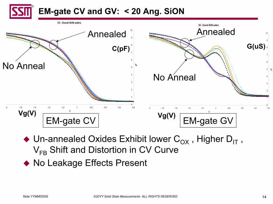
EM-gate CV and GV: < 20 Ang. SiONCV - Overall SiON wafers
0
1
2
3
4
5
6
7
8
9
10
-2 -1.8 -1.6 -1.4 -1.2 -1 -0.8 -0.6 -0.4 -0.2
V
pF
C2UA - SiONCBFA - SiONCBHA - SiONCBGA - SiONC2WA - SiONC2VA - SiONC2ZA - SiONC2YA - SiON
No Anneal
Annealed
EM-gate CV
C(pF)
Vg(V)
GV - Overall SiON wafers
0
1
2
3
4
5
6
7
8
9
10
-2 -1.8 -1.6 -1.4 -1.2 -1 -0.8 -0.6 -0.4 -0.2
V
µS
C2UA - SiONCBFA - SiONCBHA - SiONCBGA - SiONC2WA - SiONC2VA - SiONC2ZA - SiONC2YA - SiON
Annealed
No Anneal
EM-gate GV
G(uS)
Vg(V)
Un-annealed Oxides Exhibit lower COX , Higher DIT , VFB Shift and Distortion in CV CurveNo Leakage Effects Present

15
®
©20YY Solid State Measurements ALL RIGHTS RESERVEDSlide YYMMDDSS
EM-gate CV: EOT Comparison
Annealed SiON Tox Comparison
10
12
14
16
18
20
22
13 14 15 19 20 21 25
Wafer #
Tox(
Ang
.)
Specified OTox
EM-gate EOT

16
®
©20YY Solid State Measurements ALL RIGHTS RESERVEDSlide YYMMDDSS
EM-gate GV Comparison: 21 Ang. Oxides
-1.0 -0.9 -0.8 -0.7 -0.6 -0.5 -0.4 -0.3 -0.2
Vg(V)
0
1
2
3
4
5
6
7
8
9
10
Gs(
uS)
EM-gate Series GV21 Ang. SiO2 Gate Ox Preclean Matrix
Clean 1(Std): Dit = 1.11E11 cm-2 eV-1Clean 2: Dit = 3.81E11 cm-2 eV-1 Clean 3: Dit = 4.89E11 cm-2 eV-1Clean 4: Dit = 7.00E11 cm-2 eV-1
17
®
©20YY Solid State Measurements ALL RIGHTS RESERVEDSlide YYMMDDSS
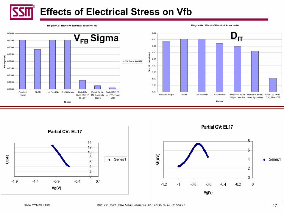
Effects of Electrical Stress on VfbEM-gate CV: Effects of Electrical Stress on Vfb
0.0000
0.0050
0.0100
0.0150
0.0200
0.0250
0.0300
0.0350
0.0400
StandardRecipe
No PB Use Fixed Nb R = 300 mV/s Partial CV,Fixed Cfb(-1.1
to -.5V)
Partial CV, NoPB, 0 sec light
delays
Partial CV(-.95to -.7 V), Fixed
CFB
Recipe
Vfb
Sigm
a(V)
5 Pt Same Site RPT
EM-gate GV: Effects of Electrical Stress on Dit
5.00
5.50
6.00
6.50
7.00
7.50
8.00
8.50
9.00
9.50
Standard Recipe No PB Use Fixed Nb R = 300 mV/s Partial CV, FixedCfb(-1.1 to -.5V)
Partial CV, No PB,0 sec light delays
Partial CV(-.95 to -.7 V), Fixed CFB
Recipe
Dit(
x 1E
11 c
m-2
eV-
1
VFB Sigma DIT
Partial GV: EL17
0
2
4
6
8
-1.2 -1 -0.8 -0.6 -0.4 -0.2 0
Vg(V)
G(u
S)Series1
Partial CV: EL17
02468
101214
-1.9 -1.4 -0.9 -0.4 0.1
Vg(V)
C(pF
)
Series1

18
®
©20YY Solid State Measurements ALL RIGHTS RESERVEDSlide YYMMDDSS
MOSCAP IV: SiON Leakage Current Comparison
1000 C Anneal SiON Wafers
1.00E-08
1.00E-07
1.00E-06
1.00E-05
1.00E-040 5 10 15 20 25 30
Nitridization Time(sec)
Leak
age
Cur
rent
(A
Vg = -2.0 VVg = -1.0 V
Un-annealed Leakage Current(Vg = -1.0 V)

®
MOSCAP IV Example A: 8 to 17 Ang. SiO2
-2.0 -1.8 -1.6 -1.4 -1.2 -1.0 -0.8 -0.6 -0.4 -0.2 -0.0
Vg(V)-10
-9
-8
-7
-6
-5
-4
-3
I(Am
ps)
EM-gate IV Comparison
EOT = 8.2 Ang.EOT = 10.2 Ang.EOT = 13.2 Ang.EOT = 16.7 Ang.

®
EM-gate IV Example A: 8 to 17 Ang. SiO2 & SiON
EM-gate Leakage Current, (Vg = -1.8 V)50 % Cumulative Probability for SiO2 & SiON groups
y = 0.0269e-0.6921x
R2 = 0.9988(3.33 Ang./Decade)
y = 0.0388e-0.6548x
R2 = 0.9975(3.52 Ang./Decade)
1.E-08
1.E-07
1.E-06
1.E-05
1.E-04
1.E-03
5 10 15 20
OTox(Ang.)
Leak
age
Cur
rent
(Am
ps)
SiO2 SiON Expon. (SiO2) Expon. (SiON)
slot 1
slot 2
slot 3
slot 5
slot 8
slot 7
slot 6
slot 4

21
®
©20YY Solid State Measurements ALL RIGHTS RESERVEDSlide YYMMDDSS
EM-gate vs Polysilicon Gate IV Leakage Correlation
Polysilicon Gate
EM-g
ate

22
®
©20YY Solid State Measurements ALL RIGHTS RESERVEDSlide YYMMDDSS
EM-gate CV, GV: Scribe Line Test Areas on Patterned Wafer
80 µm x 120 µm Test Area
CG-V curve of patterned wafer
0
1
2
3
4
5
6
7
8
-2.5 -2 -1.5 -1 -0.5 0Vg(V)
C(p
F), G
(uS)
Capacitance in pF
Conductance in uS
CV and GV Measurements
CMOS Product Wafer

23
®
©20YY Solid State Measurements ALL RIGHTS RESERVEDSlide YYMMDDSS
EM-gate MOS CV: High k Dielectrics
Page 2
50 A Al2O3
-3 -2 -1 0 1 2 3
Gate Voltage(V)
0
2
4
6
8
10
12
14
16
18
20
C(p
F)Elastic Probe CV Curve ComparisonHigh K Dielectrics(25 to 200 Angstroms)
30 A Al2O3
200 A ZrO2
25 A HfO2
50 A HfO2

24
®
©20YY Solid State Measurements ALL RIGHTS RESERVEDSlide YYMMDDSS
Summary
FastGateTM Technology • Is Rapid(60 Wafers/Hr)• Is Repeatable• is Non-damaging and non-contaminating• Can measure Oxides and Oxynitrides as thin as 7 Ang.• Can measure Product Wafers
EM-gate CV and IV Capability Includes• CET, EOT• VFB and VT,CV• DIT• Delta VFB Hysteresis• NSURF and Carrier Density Profile• Leakage Current• IV Profile
Applications on thin SiO2 , SiON with EOT values between 8 Ang. and 20 Ang. have been shown