IMPROVING ELECTRONICS ASSEMBLY PROCESS … Presentations/C/C1.pdfIMPROVING ELECTRONICS ASSEMBLY...
21
IMPROVING ELECTRONICS ASSEMBLY PROCESS THROUGH ORGANIC-METAL FINAL FINISH Rita Mohanty 401-265-0360 1
Transcript of IMPROVING ELECTRONICS ASSEMBLY PROCESS … Presentations/C/C1.pdfIMPROVING ELECTRONICS ASSEMBLY...
IMPROVING ELECTRONICS ASSEMBLY PROCESS THROUGH ORGANIC-METAL
FINAL FINISH
Rita Mohanty
401-265-0360
1
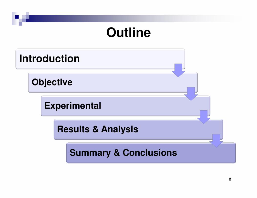
Outline
Introduction
Objective
Experimental
Results & Analysis
Summary & Conclusions
2
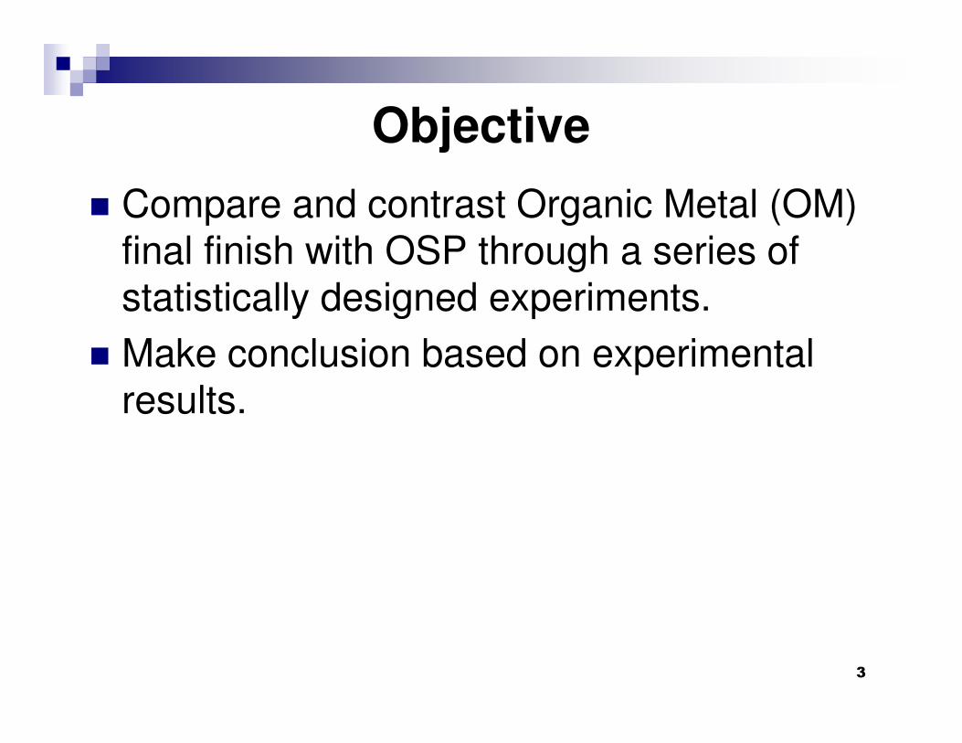
Objective
� Compare and contrast Organic Metal (OM) final finish with OSP through a series of statistically designed experiments.
� Make conclusion based on experimental results.
3
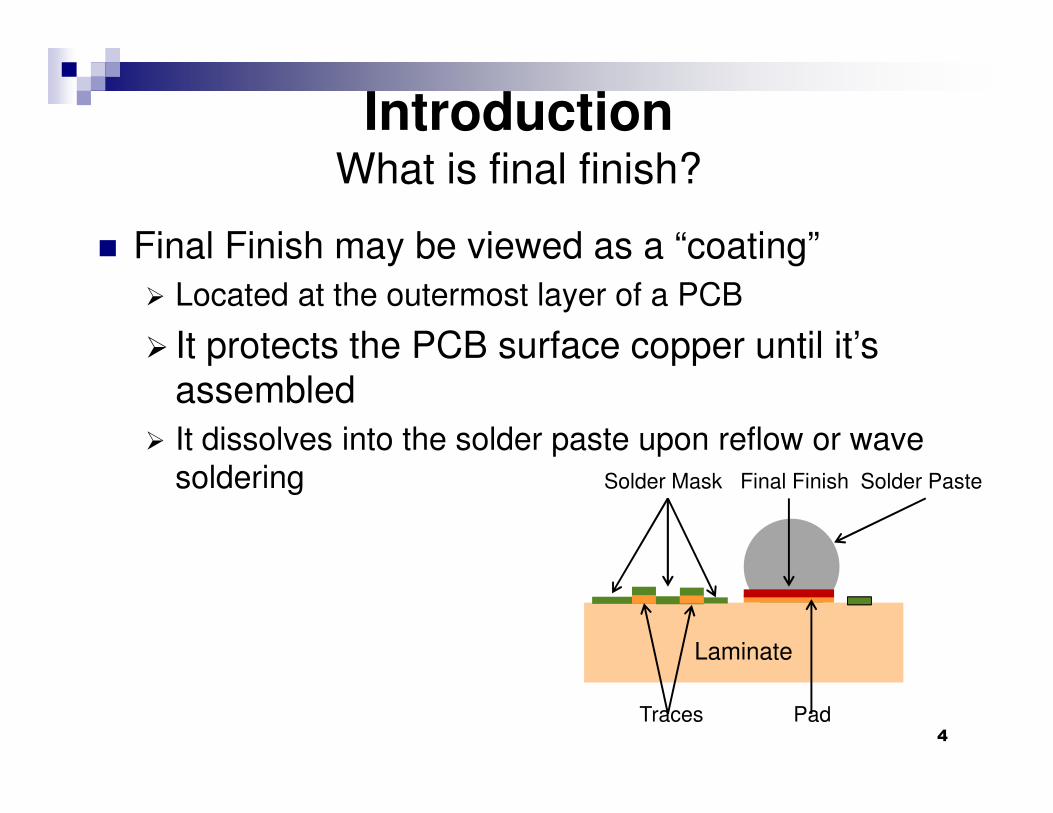
IntroductionWhat is final finish?
� Final Finish may be viewed as a “coating”
� Located at the outermost layer of a PCB
� It protects the PCB surface copper until it’s assembled
� It dissolves into the solder paste upon reflow or wave soldering
Laminate
Solder Mask Final Finish Solder Paste
Traces Pad4
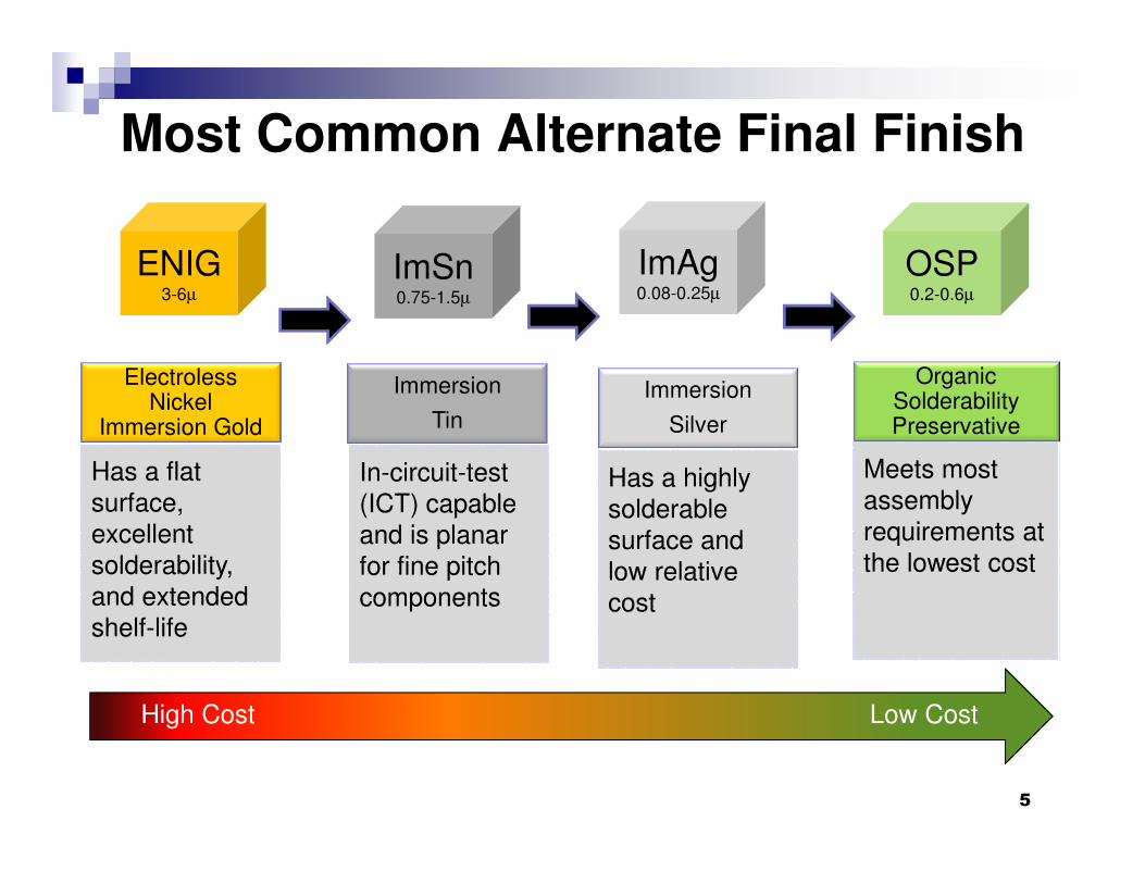
Organic SolderabilityPreservative
Meets most assembly requirements at the lowest cost
Meets most assembly requirements at the lowest cost
ElectrolessNickel
Immersion Gold
Most Common Alternate Final Finish
Immersion
Silver
Immersion
Tin
Has a flat surface, excellent solderability, and extended shelf-life
Has a flat surface, excellent solderability, and extended shelf-life
Has a highly solderablesurface and low relative cost
Has a highly solderablesurface and low relative cost
In-circuit-test (ICT) capable and is planar for fine pitch components
In-circuit-test (ICT) capable and is planar for fine pitch components
High Cost Low Cost
5
OSP0.2-0.6µ
ENIG3-6µ
ImAg0.08-0.25µ
ImSn0.75-1.5µ
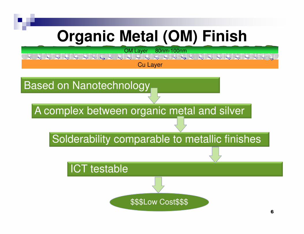
Organic Metal (OM) Finish
Based on Nanotechnology
Cu Layer
OM Layer 80nm-100nm
A complex between organic metal and silver
Solderability comparable to metallic finishes
ICT testable
$$$Low Cost$$$6
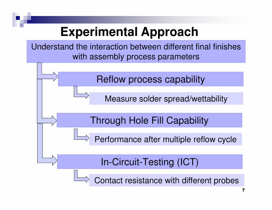
Experimental ApproachUnderstand the interaction between different final finishes
with assembly process parameters
Reflow process capability
Measure solder spread/wettability
Through Hole Fill Capability
Performance after multiple reflow cycle
In-Circuit-Testing (ICT)
Contact resistance with different probes7
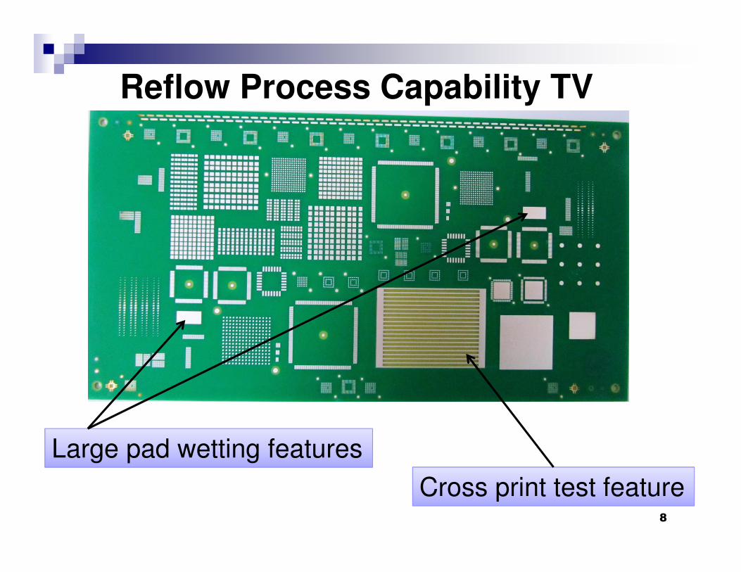
Reflow Process Capability TV
Cross print test feature
Large pad wetting features
8
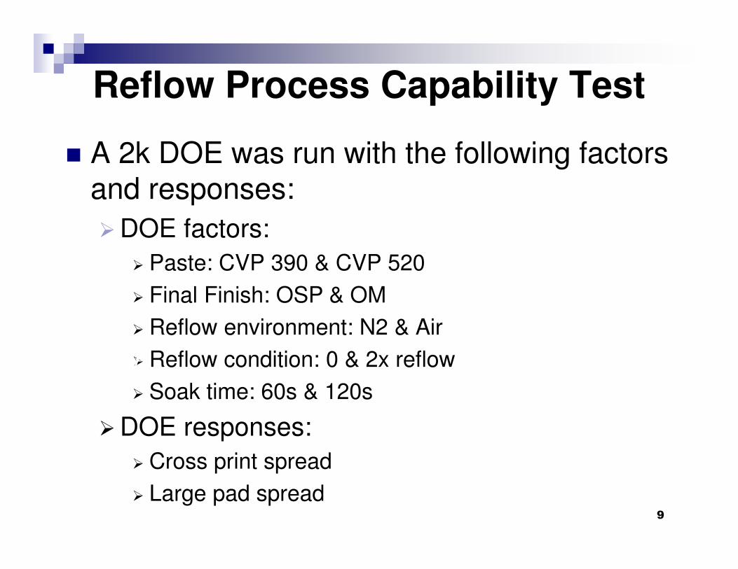
Reflow Process Capability Test
� A 2k DOE was run with the following factors and responses:
�DOE factors:
� Paste: CVP 390 & CVP 520
� Final Finish: OSP & OM
� Reflow environment: N2 & Air
� Reflow condition: 0 & 2x reflow
� Soak time: 60s & 120s
�DOE responses:
� Cross print spread
� Large pad spread
TV1
TV3
9
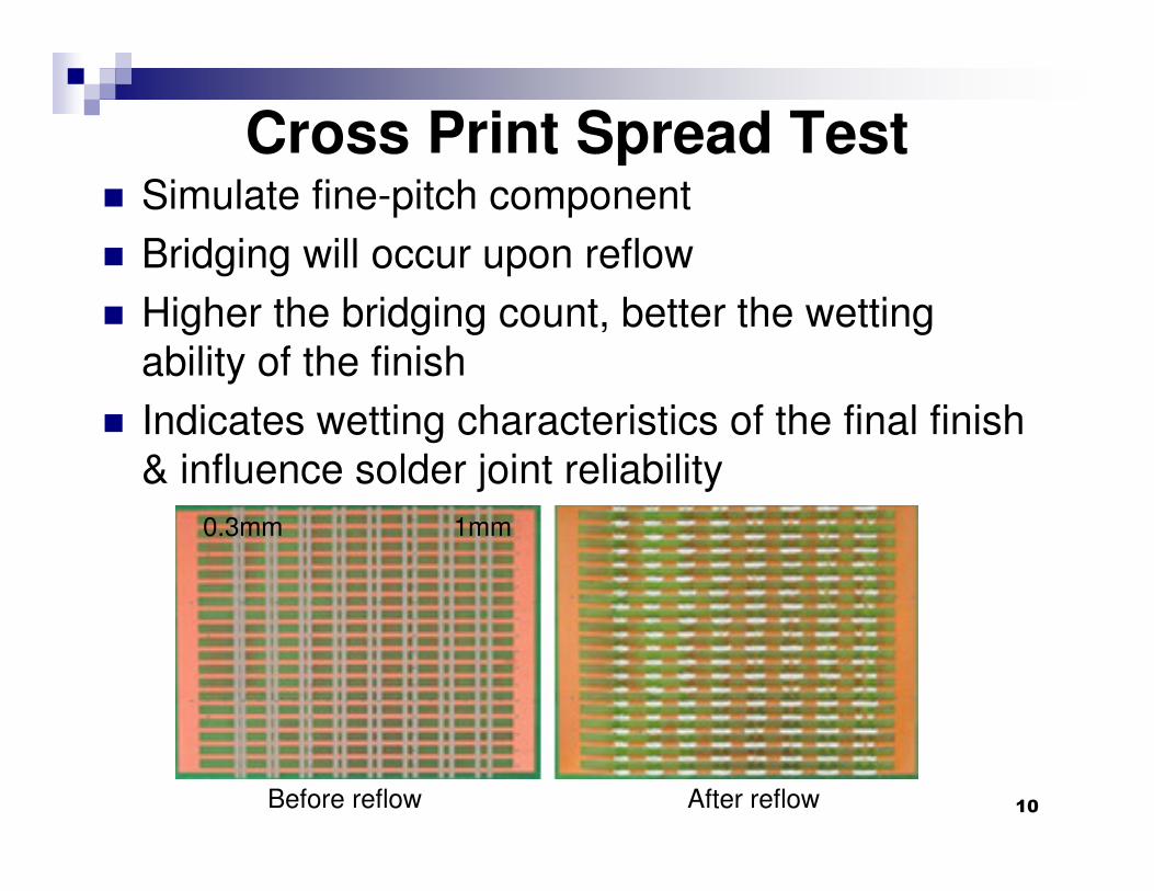
Cross Print Spread Test� Simulate fine-pitch component
� Bridging will occur upon reflow
� Higher the bridging count, better the wetting ability of the finish
� Indicates wetting characteristics of the final finish & influence solder joint reliability
TV1
TV3
0.3mm 1mm
Before reflow After reflow 10
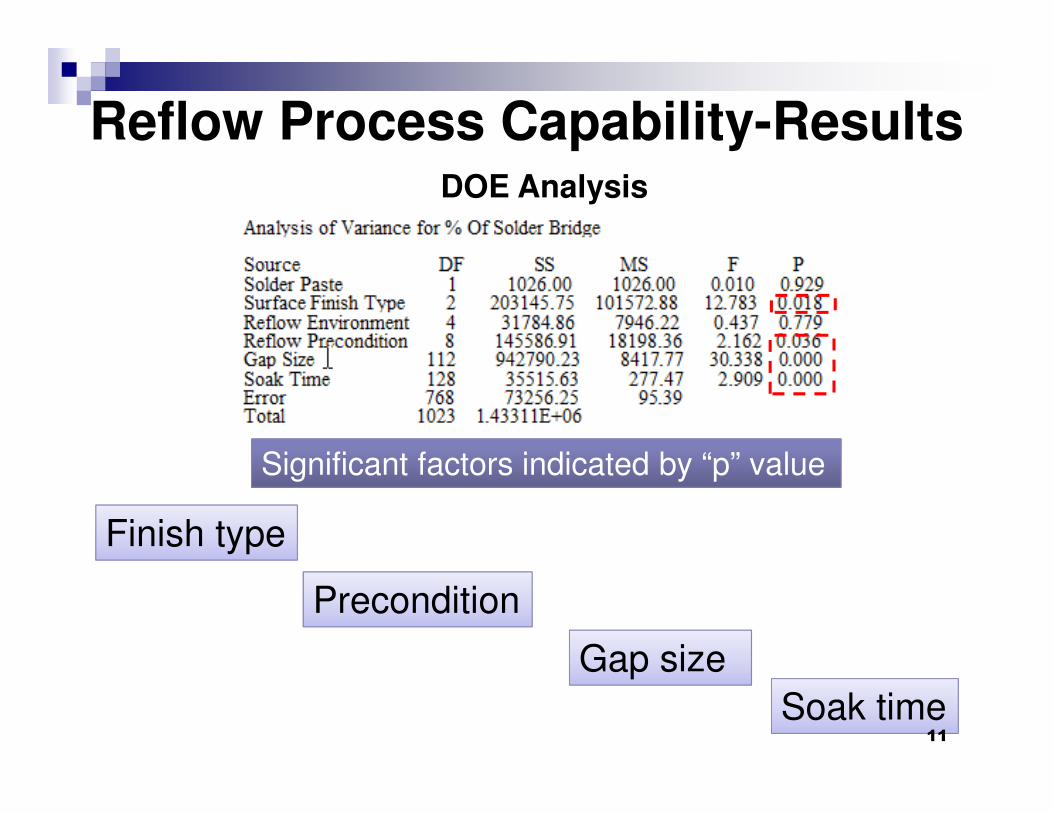
Reflow Process Capability-ResultsDOE Analysis
Significant factors indicated by “p” value
Finish type
Precondition
Gap size
Soak time11
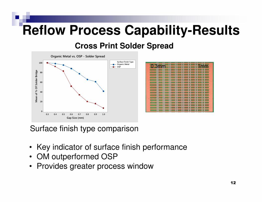
Reflow Process Capability-Results
1.00.90.80.70.60.50.40.3
100
80
60
40
20
0
Gap Size (mm)
Mean
of
% O
f S
old
er
Bri
dg
e
Organic Metal
OSP
Surface Finish Type
Organic Metal vs. OSP - Solder Spread
• Key indicator of surface finish performance• OM outperformed OSP • Provides greater process window
Surface finish type comparison
Cross Print Solder Spread
12
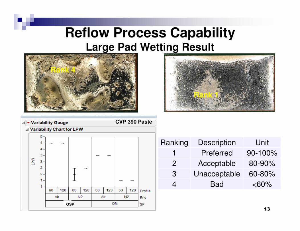
Reflow Process CapabilityLarge Pad Wetting Result
Rank 1
Rank 4
Ranking Description Unit
1 Preferred 90-100%
2 Acceptable 80-90%
3 Unacceptable 60-80%
4 Bad <60%
OSP
CVP 390 Paste
13
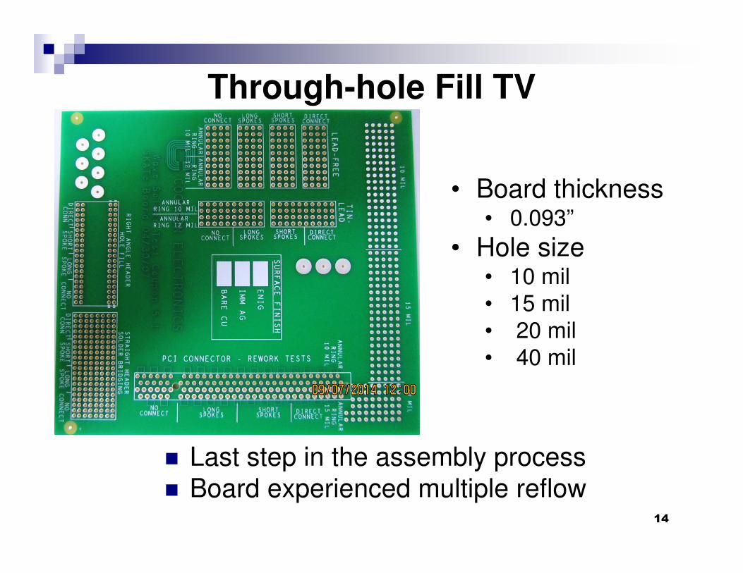
Through-hole Fill TV
• Board thickness • 0.093”
• Hole size• 10 mil• 15 mil• 20 mil• 40 mil
� Last step in the assembly process� Board experienced multiple reflow
14
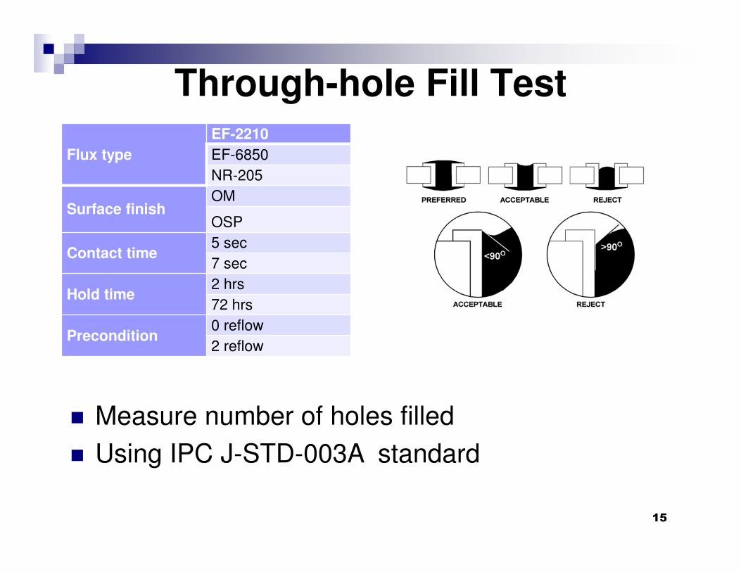
Through-hole Fill Test
Flux type
EF-2210
EF-6850
NR-205
Surface finishOM
OSP
Contact time5 sec
7 sec
Hold time2 hrs
72 hrs
Precondition0 reflow
2 reflow
� Measure number of holes filled
� Using IPC J-STD-003A standard
15
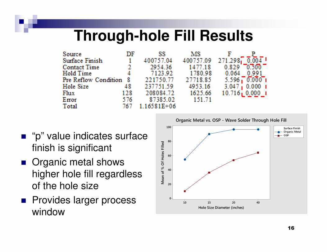
Through-hole Fill Results
40201510
100
80
60
40
20
0
Hole Size Diameter (inches)
Mean
of
% O
f H
ole
s Fil
led
Organic Metal
OSP
Surface Finish
Organic Metal vs. OSP - Wave Solder Through Hole Fill
� “p” value indicates surface finish is significant
� Organic metal shows higher hole fill regardless of the hole size
� Provides larger process window
16
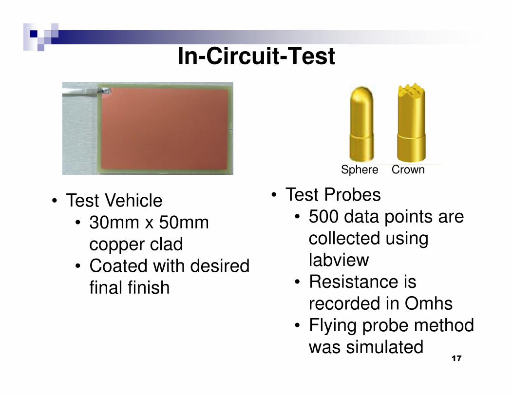
In-Circuit-Test
Sphere Crown
• Test Vehicle• 30mm x 50mm
copper clad• Coated with desired
final finish
• Test Probes• 500 data points are
collected using labview
• Resistance is recorded in Omhs
• Flying probe method was simulated
17
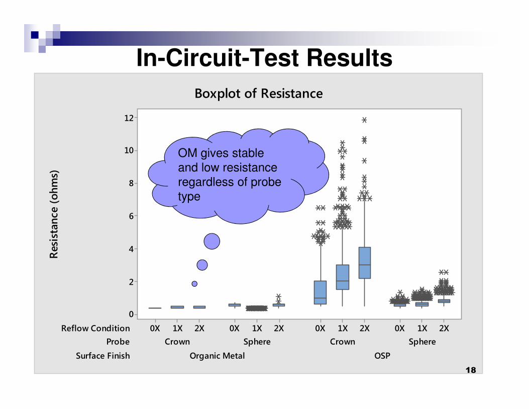
Surface Finish
Probe
Reflow Condition
OSPOrganic Metal
SphereCrownSphereCrown
2X1X0X2X1X0X2X1X0X2X1X0X
12
10
8
6
4
2
0
Resi
stan
ce (
oh
ms)
Boxplot of Resistance
In-Circuit-Test Results
OM gives stable and low resistance regardless of probe type
18
Summary
� A series of statistically designed experiments were carried out to compare OSP performance with OM
� Based on this study we can say OM has many advantages over OSP� Better wetting characteristic leading to greater solderability
� Better visual characteristic
� Wider process window
� Better ICT performance leading to elimination of false positive
� ICT performance makes OM final finish a highly desired finish as compare to OSP
� Lower cost point make OM highly desired over other metal finish without compromising performance
19
Conclusion
� PCB final finish has significant effect on the reliability, process yield, and ultimately, cost
� Choice of final finish depends on many factors
� When a visible and conductive finish is desirable, OM provides a low cost alternative to metal finish
20
Acknowledgement
I like to acknowledge my co-authors, John Fudala and Sathiya Narayanan for their relentless support in in preparing this presentation. Without their support, this paper and presentation would not have happened.
21