Improvements of Electro-optis Deflectors minimum width required at the exit, Dexit must satisfies...
47
CARNEGIE MELLON Department of Electrical and Computer Engineering~ Improvements of Electro-optic Deflectors Jie Zou 1996 Advisor: Prof. Lambeth
Transcript of Improvements of Electro-optis Deflectors minimum width required at the exit, Dexit must satisfies...

CARNEGIE MELLONDepartment of Electrical and Computer Engineering~
Improvements of Electro-opticDeflectors
Jie Zou
1996
Advisor: Prof. Lambeth

Improvements to Electro-optic Deflectors
Jie Zou
Departmentof Electrical and Computer EngineeringCarnegie Mellon University
Fall 1996
Advisor: Dr. T.E. Schlesinger
Co-advisor: Dr. D.D. Stancil
Submitted in partial fulfillment of the requirements of the degree of Master of Science in ElectricalEngineering

Acknowledgments
Personal thanks is given to my advisors, Prof. T.E. Schlesinger and Prof. D.D. Stancil for their
knowledge, advice, encouragement, and guidance. Special thanks goes to Yi Chiu, Anna Chernakova,
Venkat Gopalan, Matthew Kawas, and Jun Li for the invaluable discussion, suggestion and assistance. I
would like to thank Prof. S. Tan for his assistance and suggestions regarding lithium tantalate
deposition. Special thanks is given to Mark Mescher and Takeshi Abe for their assistance in using the
sputtering machine. I would also like to thank many graduate students and postdoctors who provided
technical assistance, suggestions, and help, especially Wei Yang and Jing Zhang. Finally, I would like to
thank Betty, Anne, Meg, Elaine, Lynn and all the others for the tremendous help and kindness which
they have given.
This project was supported in part by the Advanced Technology Program of the Department of
Commerce through a cooperative grant to the National Storage Industry Consortium (NSIC), the
National Science Foundation, and Carnegie Mellon University.

Abstract
Towards improving the performance of electro-optic (EO) beam deflectors, three major topics have been
addressed. First, theoretical analysis of an EO deflector with an arbitrary geometry has been presented.
Design of an optimal horn-shaped deflector for a given input Gaussian beam has been achieved. Horn-
shaped and trapezoidal deflectors have been shown to have better performance than traditional
rectangular ones. The effect of external optics on the number of resolvable spots for a given deflector has
also been discussed. Second, thin f’dm waveguide EO deflectors have been shown to have the potential
to increase the deflection sensitivities and to lower the operating voltages. C-orientation dominated
lithium tantalate thin films have been deposited by rf magnetron sputtering on silicon substrates. The
silicon nitride underlayers have been shown to be critical to control the lithium tantalate texture. Finally,
the optical modes and losses for deposited c-oriented lithium niobate thin film planar waveguides on
silicon substrates have been examined. A theoretical model for multi-layer planar waveguide structures
with complex propagation constants has been established and used for the numerical calculation of the
optical losses due to substrate coupling.

Table of Contents
Section
Section
2.1
1 Introduction ................................................................................. 12 Nonrectangular EO Deflectors ........................................................ 2
Analysis of an EO Prism Deflector .............................................................. 2
2.1.1 Analysis Using Snell’s Law .............................................................. 2
2.1.2 Analysis Using an Equivalent Index-graded Deflector Model ...................... 4
2.2 Rectangular Deflectors ............................................................................ 5
2.3 Trapezoidal Deflectors ............................................................................ 9
2.4 Optimal Horn-shaped Deflectors ................................................................. 12
2.5 Discussion of the Number of Resolvable Spots ............................................... 15
2.5.1 Maximum Number of Resolvable Spots ................................................ 15
2.5.2 Effect of External Optics .................................................................. 16
2.5.3 Pivot Point ...................... , ............................................................ 18
2.5.4 Maximum Number of Resolvable Spots for a Horn-shaped Deflector ............. 21
Section 3 Lithium Tantalate Thin Films for EO Deflectors ............................... 23
3.1 Thin Film Waveguide EO Deflectors ............................................................ 23
3.2 Deposition of Lithium Tantalate Thin Films .................................................... 24
3.2.1 Experiments ................................................................................ 24
3.2.2 Results and Discussion ................................................................... 25
Section 4 Optical Waveguide Characteristic of Deposited Lithium Niobate
Thin Films ................................................................................... 28
4.1 Theoretical Calculations of Complex Propagation Constants of Multi-layer
Planar Waveguides on High Index Substrates ................................................. 28
4.1.1 Theoretical Model .......................................................................... 28
4.1.2 Numerical Calculations .................................................................... 32
4.2 Measurements of Propagation Constants ....................................................... 36
4.3 Measurements of Propagation Losses ........................................................... 37
4.3.1 Sliding Prism Method ..................................................................... 37
4.3.2 Scattering Detection Method .............................................................. 38
Section 5 Summary ..................................................................................... 40

Section 1 Introduction
Optical beam deflectors are of interests for applications such as displays, switching, printing and data
storage. Among different categories, electro-optic (EO) deflectors have high bandwidth, low insertion
loss and low power consumption, which make them suitable for applications that require high speed and
modest deflection.
EO deflectors are typically rectangular in shape. This geometry limits the maximum deflection of an EO
scanner because the deflected beam has to be confined within the device. Performance can be increased
by using a nonrectangular geometry such as a trapezoidal or horn-shaped deflector, which has a wider
aperture at the exit to accommodate the displaced beam while maintaining a narrower input aperture for
higher deflection sensitivity [1], and this is presented in Section 2. The concept of pivot point and the
maximum number of resolvable spots for a deflector are also discussed in Section 2.
The earliest EO beam deflectors using bulk EO crystals were generally large, heavy, and required very
high driving voltage [2]-[4]. Significant improvements have been achieved by using wafer substrates
[5][6]. However, the thickness of the substrates cannot be very small because thin wafers are hard to
handle in processing. Therefore, these EO deflectors based on wafer materials still require relatively high
voltage to operate. Thin film waveguide EO scanners, in contrast, are capable of achieving much higher
deflection sensitivities and lower operating voltages due to their very thin structures. C-oriented lithium
niobate (LiNbO3) and lithium tantalate (LiTaO3), both of which are excellent EO materials, have
deposited on sapphire or bare silicon substrates [7]-[9]. However, the insulating sapphire substrates
cannot achieve electrically thin structures and LiNbO3 or LiTaO3 optical waveguides cannot be formed
on bare silicon substrates. Recently, the deposition of c-oriented LiNbO3 planar waveguides on silicon
substrates using a combined silicon dioxide/silicon nitride cladding layer has been reported [10]. This
structure is ideal for thin film EO deflectors. The optical properties of these waveguides are analyzed in
Section 4. Deposition of LiTaO3 thin films using a similar method is discussed in Section 3.

Section 2 Nonrectangular EO Deflectors
2.1 Analysis of an EO Prism Deflector
2.1.1 Analysis Using Snell’s Law
A simple formula for the deflection angle for a rectangular EO deflector is given by Yariv [11]. This
formula is applicable to linearly-graded index deflectors and is derived using a model based on the phase
retardation associated with straight paths through the deflector at different locations along the width of
the device. This formula is often assumed to apply for prism deflectors also. EO prism deflectors can
also be analyzed by using Snell’s law. When the maximum difference between the refractive indices of
adjacent prisms is small, which means the deflection angle is small, a simple formula can be derived.
Considering one interface first, as shown in Fig. 2.1, we have
(no + An) sin(~ - 0) = nsin~ (2.1)
Fig. 2.1 Deflection of a beam at a dielectric interface
where 0 is the deflection angle, ~x is the supplementary angle of q~ which is the angle between the
interface and the input beam, no is the refractive index in the absence of the electric field and An is the
maximum refractive index difference across the interface. Using sin0 = 0 and cos0 = 1 as 0 is small,
and q~ + o~ = 90°, the deflection angle is found as
0 = Ancot (p (2.2)

For a prism scanner with m interfaces, in the paraxial approximation, the total deflection angle inside the
crystal isAnm
0 = m ~cot tpi (2.3)no i=l
where (Pi is the angle between the ith interface and the input light. This formula can be applied for prism
deflectors with any geometry in the paraxial condition. The external deflection angle 0’ is related to 0 by
Snell’s law sin0 0----=no.sin0 0
The number of resolvable spots of the deflector is defined by Yariv as [11]
O (2.4)NO = 20div
where 0div is the far-field divergence angle of the input Gaussian beam given by
(2.5)7~0
~ is the free space wavelength and 2o~ is the waist of the Gaussian beam. Eq. (2.4) gives the number
of resolvable spots for a deflector in the far field. One should notice that Eq. (2.4) differs from Yariv’s
definition by a factor of 2 because we assume here that single-polar voltages are applied while Yariv
assumed that bipolar voltages were used.
no+An
Fig. 2.2 Rectangular prism deflector
For a rectangular prism deflector, as shown in Fig. 2.2, the internal deflection angle is related to the total
length L and the width D of the scanner as

m m AnL0=~ cotcpi= ="
no no i=~D =~-= no D
which is the same as Yariv’s formula.
(2.6)
2.1.2 Analysis Using an Equivalent Index-graded Deflector Model
It has been shown, both analytically and by simulation, that a rectangular prism deflector with a width of
D and a maximum refractive index difference of z~, is equivalent in performance to a rectangular index-
graded deflector with a linear transverse gradient of refractive index [4][12]
- (2.7)dx D
A prism deflector with an arbitrary contour W(z) as shown in Fig. 2.3 can be viewed as the combination
of many small rectangular deflectors and thus is equivalent to an index-graded deflector with a transverse
index distribution ofdn_ An (2.8)ax 2W(z)
The original input beam is along the z-axis. It is obvious that for the condition for Eq. (2.8) to
accurate one must have as many interfaces in the prism deflector as possible.
dnThe optical ray trajectory X(z) through a medium having a transverse gradient of refractive index ~-
the paraxial condition is determined by a differential equation [13]
(2.9)dz z ndx
Therefore, the ray trac~ X(z) in a prism deflector with a shape W(z) follows
Fig. 2.3 A prism deflector with an arbitrary contour
4

dX2(z)_ An 1 (2.10)dz2 no 2W(z)
and the deflection angle 0(z) at each position z inside the scanner is given
O(z) dX(z) (2.11)
F_~1. (2.10) and (2.11) are more convenient when solving deflector problems with complicated contours,
while F~. (2.3) is more accurate when the number of interfaces in a deflector is not large.
2.2 Rectangular Deflectors
From Eq. (2.6), it is clear that the width of a rectangular scanner should be as small as possible
increase the deflection. On the other hand, the scanner has to be wide enough to contain the deflected
beam. Otherwise, only the part of the beam that is inside the prism region is deflected, and this will cause
wavefront distortion. Therefore, it is important to determine the optimum width for a rectangular
deflector.
We consider the input light to be a Gaussian beam, whose 1/e2 half width inside the deflector with a
refractive index of no satisfies
co(z) = co0~]l + I ~(z’~ ~ (2.12)L ncoono j
where 2 o0 is the lie 2 waist of the beam and zo is the position of the waist.
Using Eq. (2.10), the ray trace in a rectangular prism deflector with a width D and length L 2
X(z) = 1 an (2.13)2n0 D
Thus the displacement of the beam in the exit plane of the deflector is
X(L) = 1 An 2 _10L (2.14)2n o D 2
which implies the output beam has a pseudo-pivot point, the center of the deflector. To contain the beam,
the minimum width required at the exit, Dexit must satisfies
Dexit = X(L)+ co(L)2
Using Eq. (2.6), (2.14), and (2.15), we
= co(L)+ Jco~ (L)+ An L2Dex~tno
(2.15)
(2.16)
Eq. (2.16) was initially suggested by Matthew Kawas. The minimum width required at the entrance
the deflector can be easily seen as
Dentrance = 2(0(0)
The width of the rectangular scanner must beD = max(D~,,~.~ce ,Dexit
(2.17)
(2.18)
It has been found by BPM simulations that a deflector designed by using the above calculations suffers
from wavefront distortion. This problem can be avoided by adding a factor of 1.25 to Eq. (2.12)
actually define a 4.4% beam width which leads to a wider width of the scanner using the same
subsequent calculations.
Since the width of a deflector is related to the parameters of the input Gaussian beam, the waist 2o3o and
its position zo, the deflection angle is also a function of these parameters. Fig. 2.4 shows Dentranee,
Dexit, and the deflection angle 0, as functions of o30, for a rectangular scanner with a length of 1, 2, or 3
cm. The typical parameters of a lithium tantalate EO deflector are used: no = 2.1807 and Z~n = 0.0021
(obtained by applying 1000 V across a thickness of 150 um along c-axis of the crystal). ),0 is chosen
0.6328 um and the input light is focused at the exit plane of the scanner which means zo = L.
When o30 is very large, the divergence of the Gaussian beam is very small, and the width of the beam in
the input plane of the deflector is almost the same as that in the output plane, but both values are large.
Therefore, a wide scanner is required and the deflection angle is small. This is consistent with the fact
that Dexit is very close to Dentrance because the displacement at the exit is small. Dexit is affected by both
the waist and the displacement of the beam at the exit. As o30 becomes smaller, Dexit gets smaller when
the displacement is small. But as the displacement becomes bigger, the two factors begin to compensate
each other, which leads Dexit to eventually level off. Dentrance is just the beam width at the entrance,
which is determined by two competing factors, the waist and divergence of the beam. As o30 decreases
and 0div is not large enough, Dentranee decreases. However as o30 becomes further smaller, the
divergence eventually becomes the dominant factor and Dentrance increases.
When Dexit is larger than Dentrance, the deflection angle 0 is inversely proportional to Dexit, which
increases as o30 decreases. The maximum value of 0 occurs at the turning points when Dentrance equals to
Dexit. After that, 0 drops quickly because Dentrance increases quickly.
ff the input beam is focused at the entrance of the scanner, Dentrance will be always smaller than Dexit, as
shown in Fig. 2.5 (a). Therefore, the deflection angle 0 is always inversely proportional to Dexit, and no
sharp turning point will occur in the curve of 0 vs. o30 (Fig. 2.5 (b)). The maximum values of 0 are
than these in the case that the waist of the beam is at the exit of the deflector.
6

7.0 103
6.0 103
5.0 103
=I. 4.0 103
3.0 l0s
2.0 103
1.0 l0s
0.0
Dentranc. (L=lcm)......... Dexit (L=lcm)-- -- - D (L=2cm)..... Dexit (L=2cm)- - Dtnt~=¢~ (L=3cm)
..... Dcxit (L=3cm)
(a)
0.070
0.060
0.050
0.040
0.030
0.020
0.010
0.010 100 1000
¢-oo (lam)
(b)
Fig. 2.4 (a) the minimum entrance and exit width, (b) the external deflection angle as functions of 0,for a rectangular scanner with a length of 1, 2, or 3 cm. no = 2.1807, An = 0.0021, Xo = 0.6328 um,and the input light is focused at the exit plane of the scanner.

8.0 10~
7.0 10~
6.0 10~
5.0 103
4.0 103
3.0 10a
2.0 103
1.0 103
0.0
D_entranceLL=I, 2. & 3cm,)
......... D_exlt (L=lcm)
...... D._exit (L=2cm)-- -- - D_exit (L=3cm)
" ........;..-_ i .-_ .-..-..-_-: ....: :.:_.-.:.:.-.-.:.r.:.’.-1 10 100 1000
¢oo (~tm)
(a)
0.070
0.060
0.050
0.040
0.030
0.020
0.010
0.0
........--..-..-..’- . .
10 100 1000
o)o (~m)
(b)
Fig. 2.5 (a) the minimum entrance and exit width, (b) the external deflection angle as functions o,for a rectangular scanner with a length L of 1, 2, or 3 cm. no = 2.1807, An = 0.0021, 2to = 0.6328 um,and the input light is focused at the entrance of the scanner.

In both cases, at large values of co0, 0 is nearly proportional to L. However, at small values of coo,
increasing L doesn’t increase 0 much, because the width must be larger for a longer scanner due to the
divergence of the Gaussian beam.
The far-field number of resolvable spots, No as a function of coo is presented in Fig. 2.6. As coodecreases, No monotonically decreases despite the increase of the deflection angle, 0 before reaching its
maximum because the divergence angle, 0air increases faster than 0.
60
o 50
~ 4o
~ 30
~ 20
2; 10
, ,, I, ~ , I ~ ~ I 1 ~ I ~ I I I ~00 200 400 600 800 1000 1200 1400
coo (~m)
Fig. 2.6 Far-field number of resolvable spots for a rectangular deflector with a length of 1, 2, or 3 cm.
no = 2.1807, An = 0.0021, ~o = 0.6328 urn, and the input light is focused at the exit of the deflector.
2.3 Trapezoidal Deflectors
From the discussion in the previous section, it is clear that the rectangular deflector suffers from a less
optimal design in the sense that the constant width along the device unnecessarily reduces the deflecting
power at the front and central part of the deflector. This can be improved by using a trapezoidal
geometry, where the entrance aperture is small for large deflection and the exit aperture is large to contain
the deflected beam.
As shown in Fig. 2.7, a trapezoidal deflector has an entrance aperture of 2W0, an exit aperture of 2W1,
and m interfaces. Considering the ith interface, point (zi, xi) is on the upper boundary of the trapezoidal
deflector, which satisfies

Xi -- W0 = Wl - W0L zi
(2.19)
and point (zi-1, xi-1) is on the lower boundary of the trapezoidal deflector, which satisfies
xi_l + Wo = - Wl - W0 (2.20)L zi-~
(zi-1, xi-1) and (zi, xi) are also on the interface which intersects with the original input beam or the z-axis
at an angle 9i and thus obeys the equation
Xi -- Xi_I -" tan 9i(zi -- zi_1) (2.21)
The recurrence formula for xi can be derived from Eq. (2.19), (2.20) and (2.21)
1 -b wl -- W0 cot t~iL xi_~ (2.22)xi = 1- WI - W° cot 9i
L
Assuming every interface has the same angle with the z-axis which means 9i =9 for i = 0,1, ..., m, we
have
1+ W~ -Wo cotg/mL __ /1 W~-Woc otg/
L
(2.23)
Fig. 2.7 Trapezoidal prism deflector
Noticing Ix0 = W0 and Ix m = WI , the number of interfaces is given by
10
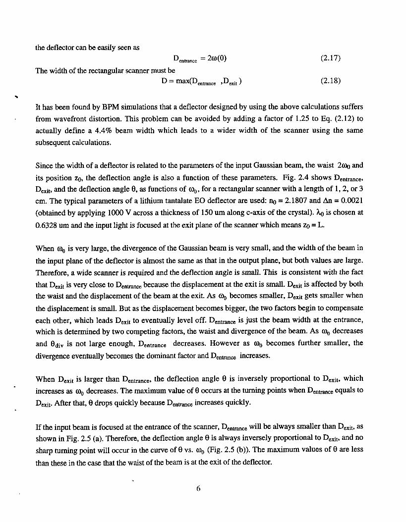
If the condition
is satisfied, we have
lnIl+
(2.24)
W~- Wo cot ~p << 1L
(2.25)
2(W~2(W’- W°)cot~ -W°) cot~L = L
1 Wl- w°cotq~ 1 W~-WocottpL L
-- 2(Wi- W0) cottp (2.26)L
Using Eq. (2.3), (2.24), and (2.26), the internal deflection angle for a trapezoidal deflector is determined
by
0 = An mcottp = An L ln(__W.l) (2.27)no no W1 - Wo w0
The approximation condition (2.25) for the above derivation implies that the more interfaces there are
the deflector, the more accurate is Eq. (2.27). This is consistent with BPM simulation results [12]. Eq.
(2.27) can also be derived by using a model of an equivalent index-graded deflector and Eq. (2.10)
(2.11) [1].
It is interesting to compare the performance of a trapezoidal deflector with a rectangular one whose width
is the average width of the trapezoidal device, i.e. D = W0 + W1. Substituting Wl with D, Eq. (2.27)
can be rewritten as
2 2w°
O~p = An L 1 ln(. D .) (2.28)no D 2- 22W° 2W°
D D
The ratio of the deflection angle for a trapezoidal deflector to that of rectangular one is thus given by
2- 2W°0~v _ 1 In( D0feet 2- 2 2W° 2W°
D D
) (2.29)
BPM simulation is used to verify Eq. (2.29) [1]. Ten interfaces are used in the simulated structure,
which are constructed such that the spacing between the two vertices of the adjacent triangular prism are
equal. The parameters for the simulation are no = 1.85012, An = 1.1xl0-4, D = 600 um, L = 1 cm, and
11

2W° from 1.0 to 0.15. The BPM simulation results are compared with Eq. (2.29) and by calculating theD
sum of the contribution from each interface using Eq. (2.3) for the trapezoidal deflector, as shown
Fig. 2.8. The agreement of the three results is quite good. As 2W----~° gets small, the curve calculated fromD
Eq. (2.3) is more consistent with the simulation than Eq. (2.29) because the condition (2.25) for
(2.29) is no longer satisfied. The deviation of the curve calculated from Eq. (2.3) from the BPM result
occurs at small 2W----9-° because the paraxial condition for Eq. (2.3) does not hold. In the context of thisD
comparison, the trapezoidal deflector has a larger deflection than a rectangular one, especially when the
input aperture is significantly reduced.
1.5
1.°I0.50
0
i I I I
o BPMEq. (2.3)
......... Eq. (2.29)
0.2 0.4 0.6 0.8 1
2W/D0
Fig. 2.8 Comparison of the deflection angle of a trapezoidal deflector and a rectangular one. The line iscalculated from Eq. (2.3), the dash line is obtained from Eq. (2.29), and the cycles are results of simulation.
2.4 Optimal Horn-shaped Deflectors
An efficient scanner requires it to be as narrow as possible and at the same time avoiding wavefront
distortion requires it to totally contain the beam. Therefore, an optimal deflector can be achieved by
designing the contour of the deflector such that the beam profile at the maximum deflection can just fit
into it, which can be expressed as
W(z) = X(z) + o(z)
12

where X(z) is the beam trace at the maximum deflection and ~(z) is the half width of the input Gaussian
beam given by Eq. (2.12). A factor of 1.25 is added to Eq. (2.12) in the following calculations to avoid
wavefront distortion. This is a coupled problem since changing the shape W(z) of the scanner will vary
the deflection and thus the ray trajectory X(z) of the beam which in turn determines W(z).
Using Eq. (2.10) and (2.30), we have a differential equation for
d2X(z) = zSm (2.31)dz2 2no X(z) + o(z)with the initial condition X(0) = 0 and ~z~ = 0. Eq. (2.31) was solved numerically and the results
shown in Fig. 2.9.
400
300
200
100
0
-100
-200
-300
-400
......... W(z) Deflector contour . __
0 2000 4000 6000 8000 10000
z (ttm)
Fig. 2.9 The optimum deflector contour for an input beam focused at the exit of the deflector with mo=
30 gm, and the corresponding ray trace and lie :~ width of the beam at the maximum deflection, no =
2.1807, An = 0.0021, ~ = 0.6328 um, and L = 1 cm.
The calculated deflection angle as a function of to0, for a horn-shaped scanner optimized for each too, are
shown in Fig. 2.10. At small values of m0, the horn-shaped deflector designed for focusing the beam at
the entrance has a better performance than the one for focusing the beam at the exit. Comparing with Fig.
2.4 and 2.6, it is clear that horn-shaped scanners have larger deflection angles than rectangular ones.
13

0.14
0.12
0.10
0.080
0.060
0.040
0.020
0.0
coo (pm)
Fig. 2.10 The calculated external deflection angle as a function of o)0, for a horn-shaped scanner
optimized for each o30, with a length of 1, 2, or 3 cm. Two cases are shown: the input beam is focused atthe entrance and exit of the scanner respectively.
70 -
> 40
~ 30
~ 20
2; 10
-- hom, L=lcm......... horn, L=2cm..... hom, L=3cm
- rect, L=lcm t- - rect, L=2cm
- rect, L=3cm
0 , , I , , , I , , ~ I ~ , , I , , , I I I i I200 400 600 800 I000 1200
Fig. 2.11 Far-field number of resolvable spots for an optimal horn-shaped deflector with a length of 1,
2, or 3 cm. no = 2.1807, An = 0.0021, Xo = 0.6328 um, and the input light is focused at the entrance.
14

Fig. 2.1 1 shows the comparison of the far-field number of resolvable spots, No as a function of 030,
between a horn-shaped scanner and a rectangular one. The horn-shaped deflector extends the range of too
that has the near maximum value of No. To obtain the maximum No at large 030, 0~iv must be very small
which requires the output beam from the deflector to have a perfect wavefront. In practice, wavefront
distortion inside a deflector cannot be totally avoided. Therefore, a horn-shaped scanner can achieve a
number of spots closer to the theoretical maximum than a rectangular one.
2.5 Discussion of the Number of Resolvable Spots
2.5.1 Maximum Number of Resolvable Spots
The number of resolvable spots depends on where it is measured. Yariv’s definition [ 1 1] as Eq. (2.4)
actually describes the far-field situation and is theoretically measured at a plane that is infinitely far from
the deflector. There may be a plane in the near-field where the number of spots is larger than the far-field
value.
We construct a moder as shown in Fig. 2.12. The effect of the deflector is simplified as scanning the
input Gaussian beam through a virtual pivot point. The original direction of the beam is along the z-axis.
The beam waist is at z = 0, the pivot point is at z = z0, and the maximum deflection angle is 0.
X
Fig. 2.12 Model for the maximum number of resolvable spots of a deflector
The lie 2 half width of the Gaussian beam at a specific location is given by
15

where ao is defined as
o~(z) = o30
2
Under the paraxial approximation, the distance from the axis of the beam to the z-axis is
Therefore, the number of resolvable spots using lie 2 criterion at a particular z plane is
= = 0(z-z0)2m0 1+
Using 0N(z) = 0 to maximize N(z), we can f’md that at an optimal planeaz
N(z) reaches the maximum
2
(2.32)
(2.33)
(2.34)
(2.35)
(2.36)
(2.37)
where No is the far-field number of spots defined by Eq. (2.4). For zo = 0, Nmax = NO, but for zoO:0,
Nmax > NO. We must note that if z0 > 0, which means that the pivot point is behind the waist of the2
_aobeam, the optimal plane for Nmax, z = < 0, implying that it is located before the pivot point and thus
is unreachable in reality.
2.5.2 Effect of External Optics
This section will discuss how external optics affects the performance of a deflector. In particular, the
effect of lenses on the number of resolvable spots for a given scanner.
As shown in Fig. 2.13, a thin lens with a focal length of f is located after the deflector. Its maximum
deflection angle is 0 and the waist of the input beam is 200. The distances from the waist and the pivot
point of the input beam to the lens are ll and 12 respectively. The waist and the maximum deflection angle
of the output beam past the lens are 200’ and 0’. The distances from the waist and the pivot point of the
output beam to the lens are ll’ and 12’ respectively. Under the paraxial and thin lens approximation, the
16

relations between 0, 0’, 12, and 12’ can be obtained by using ABCD matrices as
0=1- 0
12 -- ~12-f
Fig. 2.13 Effect of adding a lens after a deflector
(2.38)
(2.39)
Using the ABCD law and q-parameters for Gaussian beams, we havef
(00 =t’Oo/(~ __f~2 211 ~ + ao
11 =f+(ll -- f)2 + a20
The far-field divergence angle of the output beam is
, _ + aoOdiv = 7"-
f~{0o
Thus the number of spots in the far-field after the lens is
¯ 1~ - flN= =NO
20div ~/(1,- f)2 + a20
0div
To maximize N’
11 =f
is required, which minimizes 0div’, and we have
N=N0 -ao
(2.40)
(2.41)
(2.42)
(2.43)
(2.44)
(2.45)
17

If
is satisfied, we have N’ > N, which means the far-field number of resolvable spots is increased.
Combining Eq. (2.44) and Eq. (2.46), one condition for improvement in far-field number of spots
actually
Ill- 121 > a0 (2.47)
which means the waist and the pivot point of the input beam must be well separated compared to the
parameter a0. Another condition, which is expressed by Eq. (2.44), requires that the waist is located
the focal plane of the lens.
The scanning distance of the output beam at the its waist plane is given by
1 ’ ’10’d= ~ -12 (2.48)
The near-field number of spots using lie 9- criterion at this plane is
= = _ (1’ - f)(l:z-f), ..,
If we put the pivot point of the input beam in the front focal plane of the lens, which means
12 = f
we have
(2.49)
(2.50)
N = 1+ (2.51)
Eq. (2.51) is actually equivalent to Eq. (2.37), which implies that adding a lens does not change
maximum number of resolvable spots for a deflector. However, it still provides the following
advantages: first, the optimal plane can be translated to the plane where the spot size is the minimum,
which is desirable for most near-field applications; second, in the case that the optimal plane for Nraax is
unreachable when the pivot point is behind the waist of the beam, adding a lens is necessary to translate
it to a reachable location; and finally, it has the potential to increase the far-field number of resolvable
spots under appropriate conditions for far-field applications.
2.5.3 The Pivot Point
The discussion in Section 2.5.1 and 2.5.2 is based on the assumption that there exists a pivot point for a
deflector, which must be verified. This issue is also important in system considerations in EO deflector
18

applications. It has been shown in Section 2.2 that the pivot point for a rectangular deflector is at the
center.
For a horn-shaped deflector, the same equivalent index-graded deflector model for a prism deflector is
used to solve this problem. Fig. 2.14 shows the normalized distance from the intersection between the
reverse extension line of the deflected output beam and the original input beam, to the entrance, of the
scanner, as a function of the deflection angle, we can see that there indeed exists a pivot point for the
deflection and its position is very stable as the deflection angle changes.
0.340
0.335
0.330
0.325
0.320
0.315
0.310
0.305
~ L=lcm
- -- - L=2cm
......... L=3cm
0.01 0.02 0.03 0.04 0.05
0 (rad)
Fig. 2.14 Normalized distance to the length of the scanner, L, from the intersection between the reverseextension line of the deflected output beam and the original input beam, to the entrance of the scanner, asa function of the deflection angle, in a horn-shaped deflector with a length of 1, 2, or 3 cm. no = 2.1807,z~a = 0.0021, 9~o = 0.6328 um, and 03o= 30 um which is at the exit plane of the scanner.
Fig. 2.15 presents the normalized distance from the pivot point to the entrance, for a horn-shaped
deflector as a function of 030. For large 030, the pivot positions are almost at the center of the scanner,
which is because the horn-shape optimized for a large waist is actually very close to rectangular. In the
case that the beam waist is at the entrance, as 030 decreases, the entrance becomes narrower and the exit
gets wider, thus more and more of the total deflection happens near the entrance and the pivot point gets
closer to the entrance. In the case that the beam is focused at the exit of the deflector, as 030 initially gets
smaller, the same happens as above. But as 030 keeps decreasing, eventually the entrance of the scanner
must be wider than the exit to confine the beam due to the divergence, thus more and more of the
deflection power comes from the region near the exit and the pivot point moves closer towards the exit.
19

0.80
0.70
0.60
0.50
0.40
0.30
0.20
0.10
~ ......... Entrance L=lcm..... Entrace L=2cm-- Entrance L=3cm-- -- - Exit L=lcm
- - Exit L=2cm- Exit L=3cm
. _ .........~-:- ?~
10 1~
0)0 (~tm)
Fig. 2.15 Normalized distance from the pivot point to the entrance, for a horn-shaped deflector with alength of 1, 2, or 3 cm, optimized for each o)0, as a function of o)0. Two cases are shown: o)0 is at the
entrance and exit of the scanner, no = 2.1807, An = 0.0021, and ~o = 0.6328 um.
If the pivot point of deflection and the waist of the beam are in a medium with a refractive index of no,
such as the case of an EO deflector, the virtual positions of the pivot point and the waist viewed in the air
will change. As shown in Fig. 2.16, the pivot point and its virtual image are away from the interface by
distances of 11 and 11’ respectively. Using Snell’s law, we have
11 tan(0 ) 0
no Air
11
Fig.2.16 The virtual pivot point of a deflected beam passing through a medium/air interface
2O

As shown in Fig. 2.17, the q-parameters of the beam are2
qo = i~----~
~2
qo=1 ~
From Eq. (2.53b) and (2.53d), we
ql = q0 + 122 p
q~ = -ql- = i~--~ + l-z- = qo +12
O30 = O30
= l-z-
(2.53a)
(2.53b)
(2.53c)
(2.53d)
(2.54a)
(2.54b)
Fig. 2.17
no
qo qo’
o3o
Air
The virtual waist of a Gaussian beam passing through a medium/air interface
2.5.4 The Maximum Number of Resolvable Spots for a Horn-shaped Deflector
If the waist of the beam and the pivot point are separated by a distance of ls inside a scanner, using Eq.
(2.37), (2.52), and (2.54b), the maximum number of resolvable spots is given
N~_~x = N0 1+ (2.55)n0a0
Using this equation and the data of the position of the pivot point, we can calculate Nmax as a function of
o30 for a horn-shaped deflector, as shown in Fig. 2.18. For large o30, a0 is very large and the factor of
-~/1 +(-’-ILIA is close to 1, thus Nmax is close to the far-field number or spots, N0 and follows its trend,knoao)
decreasing as ~oo decreases. However, as o3o becomes smaller, ao becomes smaller, the factor of
21

1 + increases, and eventually Nmax will begin to increase. Only at very small values of r.o0,
Nmax becomes larger than the maximum value of No.
100
80-- entrance, lcm......... entrance, 2cm..... entrance, 3cm-- -- - exit, lcm
~oo (lxm)
lOO{
Fig. 2.18 Maximum number of resolvable spots as a function of ~o0, for a horn-shaped deflector with a
length of 1, 2, or 3 cm, optimized for each o~o. Two cases are shown: o~o is at the entrance or exit of the
scanner, no = 2.1807, An = 0.0021, and )~o = 0.6328 um.
22

Section 3 Lithium Tantalate Thin Films for EO Deflectors
3.1 Thin Film Waveguide EO Deflectors
Conventional EO deflectors are based on bulk EO materials such as lithium tantalate (LiTaO3) and lithium
niobate (LiNbO3) bulk single crystals or wafers [2]-[6]. The thicknesses of the substrates cannot be very
small because thin wafers are hard to handle in processing. Therefore, these EO deflectors require high
voltage to operate. A thin film waveguide EO scanner, in contrast, is capable of achieving much higher
deflection sensitivities and lower operating voltages due to its very thin structure.
One possible geometry for a thin film EO deflector employs a multi-layer planar waveguide structure, as
shown in Fig. 3.1. Lithium tantalate is both the guiding layer to confine the optical modes and the active
layer to deflect the beam. The top metal electrode is patterned
TM Light In
SiO2 (0.2 um)
TM Light In
LiTaO3 (0.5
SiNx (0.2 urn)
Fig. 3.1
I L I
~ TM Light Out
PatternedElectrode
,=~ TM Light Out
SiO2 (1.0 um)
Si Substrate
Lithium tantalate thin f’drn planar waveguide EO deflector
to have triangular shapes and the silicon substrate acts as the bottom electrode. When a voltage is applied
between the two electrodes, the refractive index change is induced inside the lithium tantalate layer in the
triangular regions underneath the top electrode, which leads to the deflection of light as it passes through
these prisms. The silicon dioxide layers are the cladding layers to isolate the optical guided mode profiles
from the high index silicon substrate and the lossy metal electrode layer. The silicon nitride layer controls
,23

the texture of the LiTaO3 fdm and acts as a barrier layer to prevent Li from diffusing into the Sit2 [10].
When a given voltage V is applied across this structure, the electric field in the lithium tantalate layer can
be shown to be
E = V (3.1)
d,+~d2+~d~
where d1 and d2 are the thicknesses of the lithium tantalate and silicon nitfide layer respectively, d3 is the
total thicknesses of the two silicon dioxide layers, and el, e2, and e3 are the permitivities of lithium
tantalate, silicon nitride and silicon dioxide respectively. The deflection angle is proportional to the
electric field E. We can define an effective thickness, deft for this multi-layer structure as
deer = d~ +~d2 +~d3 (3.2a)
E = ___V (3.2b)do.Using a set of parameters as dl= 0.5 urn, d2 = 0.2 um, d3 = 1.2 um, el = 44, e2 =6.5, and e3 = 3.9,
deft is calculated as 15.4 urn. Comparing deff with a thickness of hundreds of microns for a wafer device,
a thin fflrn deflector has the potential to increase the deflection sensitivity by an order of magnitude.
3.2 Deposition of Lithium Tantalate Thin Films
3.2.1 Experiments
C-axis-oriented lithium niobate has been deposited on silicon substrates by magnetron sputtering and the
silicon nitdde underlayers have been shown to be critical to control the texture of LiNbO3 [10]. LiTaO3
has the same crystal structure and very similar lattice constants as LiNbO3 (Table 3.1) [14]. It is expected
that the deposition mechanics for LiNbO3 may also be applicable to LiTaO3.
Table 3.1 Lattice parameters of LiTaO3 and LiNbO3 [ 14]I
Crystal I cqhex (nm)
LiTaO3
I
0.5154
LiNbO3 0.5147
Ch x (rim)1.3784
1.3856
RF magnetron sputtering was used to deposit LiTaO3 thin films. A 2-inch cold-pressed powder target
was used in our experiment. The powder for the target was a mixture of congruent lithium tantalate
(Li:Ta = 48.75:51.25) and 3wt% extra Li20. The silicon nitride underlayers were predeposited by
reactive sputtering on (111) Si substrates using a silicon target and a mixture of Ar and N2 gases. The
24

sputtering parameters for depositing lithium tantalate and silicon nitride films are summarized in Table
3.2 and 3.3 respectively.
Table 3.2 Sputterin~
Target composition
Target-substrate distance
Gas content
Gas pressure
RF power
Substrate temperature
Deposition time
conditions for LiTaO3
LiTaO3 congruent powder
containing 3wt% Li20 powder
3.5 cm
Ar (75%) + 02 (25%)
5 mTorr
25 W/~ 2 in.
500 - 600 oC
10 - 20 hr.
Table 3.3
Target
Target-substrate distance
Gas content
Gas pressure
N2 flow rate
RF power
Deposition time
Sputtering conditions for silicon nitride
silicon
3.5 cm
Ar +N2
4 mTorr
variable
100 W/¢ 2 in.
35 min.
After sputtering for a predetermined time, the ~ms were cooled to room temperature at a rate of about 10
°C/min inside the sputtering chamber at an 02 flow of 58 seem and a pressure of 10 mTorr. The
resulting f’dms were analyzed by 0/20 x-ray diffraction (XRD) and atomic force microscope (AF/vl).
3.2.2 Results and Discussion
Fig. 3.2 shows the XRD patterns of three lithium tantalate films which were deposited under the same
conditions but with the silicon nitdde films deposited using different nitrogen flow rates. The XRD
spectra of LiTaO3 films deposited on silicon nitride underlayers which were deposited with N2 flow rates
of 4.0, 4.5, and 5.0 seem display peaks similar to that of LiTaO3 powder which means random
orientation, a strong (006) texture, and peaks similar to that of a random oriented texture plus a high
(006) peak respectively.
25
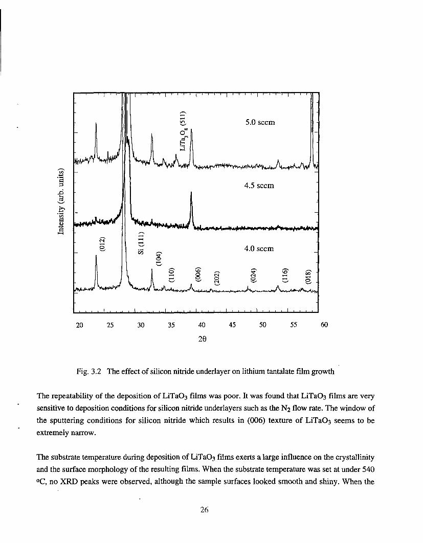
~ 5 0 sccm -
4.5 sccm
¯ .. 4.0 sccm
20 25 30 35 40 45 50 55
2O
Fig. 3.2 The effect of silicon nitride underlayer on lithium tantalate f’dm growth
The repeatability of the deposition of LiTaO3 films was poor¯ It was found that LiTaO3 films are very
sensitive to deposition conditions for silicon nitride underlayers such as the N2 flow rate¯ The window of
the sputtering conditions for silicon nitride which results in (006) texture of LiTaO3 seems to
extremely narrow.
The substrate temperature during deposition of LiTaO3 films exerts a large influence on the crystallinity
and the surface morphology of the resulting films. When the substrate temperature was set at under 540
oC, no XRD peaks were observed, although the sample surfaces looked smooth and shiny¯ When the
26

temperature of the substrate was set around 600 oC, prominent XRD peaks with narrow intrinsic widths
were observed while at the same time cracks and other defects appeared in the films. 570 oC was found
to be the optimal substrate temperature.
Fig. 3.3 shows 3-D AFM images for the LiTaO3 films grown at substrate temperatures of 540 oC and
570 °C respectively. Most features shown in the AFM image for the LiTaO3 film deposited at 540 oC are
small with a size of about 20 nm and a height of about 30 nm although afew features approach 60 nm in
size and 100 nm in height, which implies that the film just begins to crystallize. This film has a mean
roughness of 4.6 nm and a peak-to-valley value of 89 nm. The typical feature in the LiTaO3 film
deposited at 570 °C is much larger with a size of 200 nm and a height of 250 nm. The mean roughness is
67 nm and the peak-to-valley value is 300 nm for this film.
(a) (b)
Fig. 3.3 3-D AFM images for the lithium tantalate thin films deposited at the substratetemperatures of (a) 570 °C and (b) 540
27

Section 4 Optical Waveguide Characteristic of LiNbO3 Deposited Thin
Films
It is essential to characterize the optical properties of LiNbO3 sputter deposited thin film waveguides to
apply them in thin film electro-optic scanners or other optical devices.
The c-oriented LiNbO3 film, which is the guiding layer, is deposited by RF magnetron sputtering on top
of a silicon nitride undedayer that controls its orientation on silicon substrates[10]. Silicon has a higher
refractive index than that of LiNbO3 and is absorbing at the wavelength of interest (e.g. 0.6328 um).
Thus, a cladding layer is required between the LiNbO3 guiding layer and silicon substrate. Silicon nitride
could act as the buffer layer if a thick enough film could be easily grown. However, because of the stress
in the silicon nitride film primarily due to the disparity between its thermal expansion coefficient and that
of the silicon substrate, it is very difficult to grow high quality thick silicon nitride films on silicon.
Thus, another isolating layer with an index of refraction lower than that of silicon nitride is required.
Silicon dioxide is the natural choice. The whole structure is thus a five-layer slab waveguide as the air
and silicon substrate are considered to be semi-infinite. If a metal electrode on top of the LiNbO3 layer is
needed as in the structure of a thin film electro-optic scanner, another buffer layer is required to isolate
the optical modes from the lossy metal layer, and thus an even more complex seven-layer planar
waveguide structure must be analyzed.
4.1 Theoretical Calculations of Complex Propagation Constants of Multi-layer
Planar Waveguides on High Index Substrates
4.1.1 Theoretical Model
Since one of the two outer semi-infinite layers, the Si substrate in the five-layer structure that is
considered in this section has a larger refractive index than those of the other layers, the waveguide
modes are not strictly bound modes, but instead leaky modes or weakly-guiding modes. The modes are
thus characterized by complex propagation constants, with the imaginary parts corresponding to
attenuation due to optical energy radiating away from the guiding layers into the substrate [15]. If the
cladding layer is thick enough, the optical field profiles are well isolated from the higher refractive index
substrate, which means the energy loss due to the substrate can be ignored. In this situation, the solution
of the boundary value problem yields propagation constants that can be accurately approximated by the
corresponding solutions for the waveguide structure consisting of the first four layers, that is, by
omitting the high index substrate and assuming the buffer layer is semi-infinite. The propagation
constants for this four-layer structure are real, corresponding to strictly bound modes. The thicker the
28

buffer layer is, the more accurate the four-layer approximation is, and thus the smaller the loss due to the
high index substrate. However, as shown in Section 2, in order to obtain a higher electric field inside the
LiNbO3 layer by applying a particular voltage, it is desirable to have a buffer layer as thin as possible.
Therefore, one of the main tasks of this calculation is to determine the minimum thickness of the cladding
layer required which still results in a reasonably low attenuation.
The actual waveguide geometry that we consider is shown in Fig. 4.1. The refractive index of LiNbO3
used here is the accepted value for single crystal material and might be slightly different from the actual
value for a deposited thin film. The Z-axis is the light propagation direction, and the X-axis is
perpendicular to the waveguide surface.
X
air no = 1.0
lithium niobate n~ = 2.2 dl= 0.5 um
silicon niU’ide n2 = 2.0 d2 = 0.2 um
silicon dioxide n3 = 1.46 d3 variable
silicon n4 = 3.85 - 0.02i
,- (dI + d2)
,-(d I +d2+d3)
Fig. 4.1 Geometry of LiNbO3 thin film planar optical waveguide
To describe the modal behavior here, Maxwell’s equations must be solved in the five regions with the
appropriate boundary conditions applied at each interface. Since the structure is composed only of planar
layers that are considered homogenous and isotropic in the Y and Z directions, we consider propagation
in the Z direction and ignore the field variations in the Y direction. TM modes are considered here, since
with these the electro-optic deflectors can make use of the largest electro-optic coefficient r33 assuming
the LiNbO3 film is c-oriented.
TM modes are specified by solutions for the y component of magnetic field, which have the form
Hy(X, z, t) = Hy (x)e -i(l~z-t°t) (4.1)
where 13 is the complex propagation constant. For fields of this form, the scalar wave equation is reduced
to
29

d2Hy(X)dx2 + (k2n~ _ ~2)Hy(x)
Ex = ~0~i2 Hy.
1 dHy
lO~oni
(4.2a)
(4.2b)
(4.2c)
where k = 2x/% is the free-space wavenumber, % is the free space wavelength, and ni is the refractive
index of the ith layer. It is convenient to define an effective index of refraction, neff as
n¢ff = ~J/k (4.3)
We seek solutions of (4.2a) in two different ranges:
(i) z <Re(heir) < (4.4a)
which means the lightwave is guided inside layer 1, or
(ii) 3 <Re(nen,) < n2 (4.4b)
which means the lightwave is guided inside both layer 1 and 2. We consider these solutions because they
correspond to the strictly bound modes for the four-layer structure in the limiting situation where the fifth
layer is omitted and the forth layer becomes semi-inf’mite. For the situation where the real part of neff is
within range (i) stated above and where we impose radiation conditions at x = -00, solution of (4.2a)
have the form [15]
where
T, -r0xHy = rt0e ,x > 0 (4.5a)
Hy = HlCOSklX+H 1 sinklX,0 > x> -dI (4.5b)
- -r2xHy = H2e-r2x + H2 e ,-d I > x > -(d I + d2) (4.5e)
_ -r3x = -r3x . ¯Hy = H3e +1-13 e ,--(01 +d2)> x> -(dl +d2+d3) (4.5d)
= -ik4xHy = H4e ,-(,01 + 2 +d3) < x (4.5e)
r0 = k4n2etr- n20 (4.6a)
k~ = k nI - n~tr (4.6b)
2 2r2 = k4nefr - n2 (4.6c)
r 3 = k4n~fr- n~ (4.6d)
~]~ 2 (4.6e)k4 = k n - neff
kl and k4 are the transverse wavevectors in layer 1 and 4 respectively, and r0, r2 and r3 are the transverse
attenuation coefficients in layer 0, 2 and 3 respectively. The boundary conditions require the continuities
30

,,~ ldHyof tangential components of magnetic and electric fields, Hy and Ez n2 dx ’ at each dielectric
i
interface. These boundary conditions are expressed as a set of linear equations for H0, HI, H1 , H2,
H2, H3, H3, and H4, which can be written down in a matrix form
A. It = 0 (4.7)whereIt=[H 0H1 HI H2H2 H3H3 H4]Tand
1 -1 o o or-9-° 0 k--L 0 02 2no nl
0 gOskld1 -sin kld I -er2dl -e-r2dl
kl k1 r2 r2dl r20 ---~-sinkld 1 -~-cOskld1 ---~-e 2 e-r2dlnl nl n2 n2
0 0 0 er2(dl+d2) e-r2(dl+d2)
0 0 0 -- r--~-2~ er2(dl +d2)r22 e-r2
(dl+d2)
n2 n2
0 0 0 0 00 0 0 0 0
0 0 oo o o
o o oo o o
_er3 (d1 +d2 ) _e-r3 (dl +d2 0r32 er3(dl+d2)
r’~t~-r3(dl +d2) 0n3 n3
-r3 (d1 +d2 +d3 ) -ik4 (dI +d2 +d3 )er3(dl+d2+d3) e --er3 r 3 -~3(dl+d2+d3) k4 -ik4(dl+d2+d3)
2 er3(dl+d2+d3) --~-e --~-en3 n3 n4
For Eq. (4.7) to have non-zero solutions, the determinant of A must be zero
(4.8)
(4.9)
This is the eigenvalue equation for the waveguide structure. With the help of matrix operations provided
by commercial mathematical software such as MATLAB, Eq. (4.9) can be easily solved, if all the
elements of A are real, which is only true for the limiting waveguide structure. One can see that the
above method is very convenient and systematic for solving multi-layer slab waveguide problems.
For the situation where the real part of neff is within range (ii), equation (4.5) and (4.6) hold except
(4.5c) changes
Hy = H2 cosk2x+ H2 sink2x,-d~ > x > -(da + d2) (4.10c)
where2 2k2 = k4n2 - neff (4.1 lc)
Similar boundary conditions are applied and written in the same matrix form and a similar eigenvalue
equation as (4.9) is obtained, except that the elements of A are different
31

1 -1 0r--q-0 0 k--L2 2
no n10 cos kid 1 - sin kid1
0 -~-sinkld I ~-cOskld1n1 nl
0 0 0
0 0 0
0 0 0
0 0 0
k ...
0 0 0 0 0
0 0 0 0 0
-cos k2d1 sin k2d1k2 k2
--T sin k2d1 ~- cos k2d1n2 n2
cosk2(d 1 +d2) -sin k2 (d I +d2)
-~sink2(d 1 + d2) -~cOSkE(dl + E)n2 n2
0 0
0 0
4.1.2 Numerical Calculations
0 0 0
0 0 0
er3 (dl +d2 -r3 (dl +d2 -- --e 0r3 r3(dl+d2) r3 ¢-r3(dl+d2)¯ --~e 2 0
n3 n3-r3 (dI +d2 +d3) -ik 4 (dl +d2 +d3
er3(dl+d2+d3) e --er3 r 3 -r3(dl+d2+d3) k4 -ik4(dl+d2+d3)
2 er3(dl+d2+d3) -~-e--~-e
n3 n3 n4
(4.12)
The complex eigenvalue equation that must be solved can be divided into real and imaginary
components, yielding two equations with two unknowns, neffr and neffi, the real and imaginary parts of
neff. These simultaneous equations suggest a numerical solution using the Newton-Raphson method,which allows an iterative search for concurrent zeros by the first-order terms of the Taylor
expansion[16]. The system of equations
may then have approximate zeros
(4.13a)
(4.13b)
n~m = n~fno + a (4.14a)
n~ffi = ncfro + b (4.14b)
where neffr0 and neffi0 are the initial estimates, and a and b are the corrections. Using the abbreviated
Taylor expansion gives
0ReIAII 9ReIAII
In~A(nem, n~ni)l=In~A(n~,nc~)l+a Oneffr ,~om.nomo+b--~m nora.nora. (4.15b)
Solving the above equations yields the first corrections:
,0ReIAII , ,0I Alt,n ,o
32

These formulas are then applied iteratively until the zeros are determined to a desired degree of accuracy.
The initial estimate of the real part, neffr0, is provided by the eigenvalue of the limiting four-layer
waveguide structure using a similar matrix method; the initial estimate of the imaginary part, neffi0, is
taken as zero. For a waveguide structure with a relatively thick cladding layer, these initial estimates are
good enough to allow for a fast convergence. However, for a waveguide with a relatively thin buffer
layer, neffi may be quite large and the above estimates may be too far from the actual solutions, which
leads to slow convergence or even divergence. In this case, a series of pseudo-problems are artificially
created, which have a decreasing series of buffer layer thicknesses from a reasonably large one to the
actual thickness of the real problem needed to be solved. The first waveguide structure in this series with
a thick cladding layer can be solved using the above estimates. The solutions are used as the estimates for
the subsequent problem that has a little thinner isolating layer. This process is repeated until the actual
problem is solved.
For the specific waveguide structure shown in Fig. 4.1, the above method is applied to calculate the
complex effective index for each TM mode as a function of the cladding layer thickness. This waveguide
supports altogether four TM modes. Fig. 4.2 shows the real parts of neff for all TM modes. TM0 is
guided inside the LiNbO3 layer, because its Re(neff) are higher than the refractive index of silicon nitride
and lower than that of LiNbO3. TM1, TM2 and TM3 are bounded within both LiNbO3 and silicon nitride
layer, because their Re(neff)s are between the refractive index of silicon dioxide and that of silicon
nitride. The real part of neff for every TM mode remains constant until the buffer layer becomes very thin
as the disturbance of the high refractive index substrate is no longer negligible. The turning point for a
higher mode is at a larger value of cladding layer thickness, since the optical field profile of a higher
mode is less confined within the guiding layer. However, the variations of the effective indices for all the
TM modes for thin buffer layer are still very small.
Imaginary parts of neff and the corresponding losses due to the high refractive index substrate are shown
in Fig. 4.3a. As the thickness of the buffer layer decreases, the Im(neff) and corresponding loss for each
TM mode increase dramatically. At the same cladding layer thickness, the higher modes have higher
substrate coupling losses, because the optic field profiles of higher modes are less confined within the
guiding layers and thus more energy is coupled into the substrate. The loss for TM3, which is very near
cutoff (Re(neff)----~n3), is much higher than those of the other three TM modes because a
33

2.1382
2.1380
2.1378
2.1376
2.1374
2.13720.001 0.01 0.1 1
d3 (urn)
(a)1.97001 Z,.
1.96801.9670
1.96601.9650
1.96401.9630
1.9620 ........0.001 .0.01 0.1
d3 (um)
1.7700
1.7600
1.7500
1.7400
1.7300
(b)
1 10
1.7200 ........ ~ ........ ~ ........ v .......0.001 0.01 O. 1 1 10
d3 (urn)
(C)
1.4850
1.4800 --
1.4750 --
~ 1.4700
1.4650
1.4600
1.4550
0.001 0.01 0.1 1 10d3 (urn)
(d)Fig. 4.2 Real parts of effective indices for (a) TM0, (b) TM1, (c) TM2, and (d) TM3 mode waveguide structure as shown in Fig. 4.1 as functions of the buffer layer thickness.
34

approaching cutoff has the most spread optical field profile. From Fig. 4.3b, it can be seen that about 3.6
um cladding layer is required for all the TM modes to have reasonably low substrate coupling loss (<
dB) and only about 0.3 um is required for TM0 mode.
10°
10-2
10-8
~TM3
(a)
10s
103
10~
10-~
0 1 2 3 4 5d3 (um)
(b)
Fig. 4.3 (a) Imaginary parts of effective indices and (b) substrate coupling losses for TM0, TM1, and TM3 mode of the waveguide structure as shown in Fig. 4.1 as functions of the buffer layerthickness.
35

4.2 Measurements of Propagation Constants
The propagation constants of the guided modes are measured by using the prism coupling method,
which enables selective excitation of an arbitrary guided mode [17][18]. A prism with a refractive index
of np, which is higher than that of the guiding layer, is put in close proximity to a y~aveguide, with a thin
air gap between the prism and the waveguide, as shown in Fig. 4.4. A guiding wave is selectively
excited by phase matching between the incident beam and the guided mode with a propagation constant
13, which requires
~ = npksinOi (4.17)
where Oi is the angle in the prism, that is related to the angle outside the prism, 0 through Snell’s law as
sin(90° - 0 - t~) =np sin(Oi -- 0~) (4.18)
where t~ denotes the toe angle of the prism.
Fig. 4.4 Prism coupling
Fig. 4.5 illustrates the experimental setup for propagation constant measurement using prism coupling. A
45°-45°-90° mtile prism with a refractive index of 2.584 is used as the input coupling prism. The
waveguide and the prism are mounted on a rotation stage. The collimated and polarized input beam
emitted from a He-Ne laser illuminates a position near the comer of the prism. The input beam angle and
position are adjusted to excite the desired guided mode. A scattering light streak can be seen on the
waveguide surface when guided-wave excitation happens. The propagation constant of the mode is then
determined by the input angle through (4.17) and (4.18). The guided wave can be taken out by using
output coupling prism. If the output prism is the same type as the input prism, the angle of each output
beam corresponding to a guided mode will be the same as the input coupling angle for the mode. Thus
the propagation constant of each mode can also be determined by examining the output beam pattern, or
m-line. The experimental results are consistent with the theoretical calculations described in the early part
of this section, shown in Table. 4.1.
Table 4.1 Coupling angles for TM modes of the waveguide structure show asFig. 4.1 with a silicon dioxide buffer layer thickness of 8 um.
neff TM0 TM1 TM2 TM3
Measured 2.138+0.005 1.968+0.02 1.790+0.02 1.462+0.005
Theoretical 2.1373 1.9627 1.7284 1.4648
36

Fig. 4.5 Experimental setup for propagation constant measurement
4.3 Measurements of Propagation Losses
The propagation loss of the waveguide, an important parameter, can be measured by two different
methods: sliding prism method and scattering detection method.
4.3.1 Sliding Prism Method
Measurement of transmission losses by the sliding-prism method is shown in Fig. 4.6 [17]. Guided
modes are excited by a fixed input prism and the intensity of the output light coupled out by an output
prism is measured as the output prism slides toward the input prism. The output light intensity is plotted
in dB as a function of the transmission distance L in cm, and the slope of the fit is the loss in dB/cm.
Matching liquid (1-Bromonaphthalene and 1-Iodonaphthalene) with a refractive index of 1.700 + 0.002 is
used to enhance and maintain the coupling efficiency, and to reduce friction during the sliding process.
Detector
Input prism Output prism / \~
~ ~ Sliding ~
I ~ ~ I Matching liquid
Fig. 4.6 Measurement of transmission losses by the sliding prism method
A plot of normalized TM light intensity coupled out of the waveguide versus the transmission distance
for a waveguide structure as shown in Fig. 4.1 with a 8 um silicon dioxide buffer layer is present in Fig.
37

4.7. The slope of the straight line corresponds to a loss of 17.7 +0.2 dB/cm. The LiNbO3 guiding layer
is a polycrystalline film deposited by sputtering. Therefore the relatively high transmission loss of the
waveguide is probably primarily due to scattering at the grain boundaries.
30
Loss = 17.7+ 0.2dB/cm
15 , , , , | , , , , I , ~ , , I ~ , , , I , , , , I i ~ i ~
0 0.05 0.1 0.15 0.2 0.25 0.3
Distance (cm)
Fig. 4.7 Plot of normalized light intensity coupled out of the waveguide as a function of transmissiondistance for the waveguide structure as shown in Fig. 4.1 with a 8 um silicon dioxide buffer layer. Thecircles correspond to measured data using the sliding prism method and the straight line is a linear meansquare fit of the data.
4.3.2 Scattering Detection Method
The brightness of a guided wave scattered light streak is proportional to the guided mode intensity at each
point, provided that the waveguide is uniform. Measurement of the scattered light intensity distribution
along the propagation of guiding modes therefore enables determination of transmission losses [ 17]. To
detect the scattered light, a video camera is used to capture the image of the streak, as illustrated in Fig.
4.8. The field aberration of the lens system of the camera can seriously affect the measurement accuracy
of the scattered light intensity distribution. An improved method can be used, in which a series of images
of the streak are taken as the camera slides along the streak and the average of the intensities of several
central pixels in each image is used as the scattered light intensity at each position.
38

Fig. 4.8
Input prism
Sliding
JCamera
Measurement of transmission losses by the scattering detection method
Fig. 4.9 shows a plot of normalized scattered light intensity measured by the camera as a function of
transmission distance for the same waveguide measured by the sliding prism method. This data
corresponds to a loss of 18.5 +2.0 dB/cm, which is very consistent with the result obtained by using the
sliding prism method. The deviation of the data points is due to the inhomogeneity of the scattered light.
Loss = 18.5+ 2.0dB/cm
.... .... .... ....I I I I , , , | I i | | | I |
0.05 0.1 0.15 0.2 0.25 0.3Distance (cm)
Fig. 4.9 Plot of normalized scattering light intensity as a fuhction of transmission distance for thewaveguide as shown in Fig. 4.1 with a 8 um silicon dioxide buffer layer. The circles correspond tomeasured data using the scattering detection method and the straight line is a linear mean square fit of thedata.
39

Section 5 Summary
The analysis of an EO prism deflector by using an equivalent index-gradient deflector model is consistent
with the method using Snell’s law. An optimal horn-shaped deflector for a given input Gaussian beam
has been designed such that the beam at the maximum deflection just fits into the device contour.
Theoretical calculations have shown that a trapezoidal or horn-shaped deflector has a better performance
than a rectangular one. Rectangular or horn-shaped EO deflectors have been shown to have scanning
pivot points by theoretical analysis. Thin film planar waveguide EO deflectors have been shown to have
a big potential to increase the deflection sensitivities and to lower the operating voltages. C-orientation
dominated lithium tantalate thin films have been deposited on silicon substrates by RF sputtering. The
silicon nitride underlayer has been shown to be critical to determine the texture of lithium tantalate. The
lithium tantalate films were very sensitive to the deposition conditions of the silicon nitride underlayers
and the repeatability was poor. A feature size of about 200 nm on the film surfaces has been observed by
AFM. The propagation constants of TM modes for c-axis oriented lithium niobate thin film planar
waveguides on silicon substrates were measured by prism coupling and the results were consistent with
the theoretical calculation. The optical loss of this waveguide has been examined by the sliding prism
method and scattering light detection method respectively. An attenuation for TM modes of about 18
dB/cm has been obtained.
40

References
[10]
[11]
[1] Y. Chiu, "Material and optical device characterization in potassium titanyl phosphate (KTiOPO4,
KTP)," Ph.D. thesis, Chap. 2.4, Dept. of Electrical and Computer Engineering, Carnegie Mellon
Univ., 1996.
[2] V.J. Fowler, C.F. Buhrer, and L.R. Bloom, "Electro-optic light beam deflector," Proc. IEEE, vol.
52, pp. 193-4, 1964.
[3] V.J. Fowler and J. Schlafer, "A survey of laser beam deflection techniques," Appl. Optics, vol. 5,
pp. 1675-82, 1966.
[4] J.F. Lotspeich, "Electrooptic light-.beam deflection," IEEE Spectrum, pp. 45-52, 1968.
[5] Q. Chen, Y. Chiu, D.N. Lambeth, T.E. Schlesinger, and D.D. Stancil, "Guided-wave electro-
optic beam deflector using domain reversal in LiTaO3," J. Lightwave Tech., vol. 12, pp. 1401-4,
1994.
[6] J. Li, H.C. Cheng, M.J. Kawas, D.N. Lambeth, T.E. Schlesinger, and D.D. Stancil, "Electro-
optic wafer beam deflector in LiTaO3," Nonlinear Frequency Generation and Conversion, San
Jose, CA., 29-31 Jan. 1996, pp. 73-7.
[7] Y. Saito and T. Shiosaki, "Heteroepitaxial rowth of LiTaO3 single-crystal films by RF magnetron
sputtering," Jap. J. Appl. Phys., vol. 30, pp. 2204-7, 1991.
[8] N. Fujimura and T. Ito, "Heteroepitaxy of LiNbO3 and LiNb308 thin films on c-cut sapphire," J.
Cryst. Growth, vol. 115, pp 821-5, 1991.
[9] T.A. Rost, H. Lin, T.A. Rabson, R.C. Baumann, and D.L. Callahan, "Deposition and analysis of
lithium niobate and other lithium niobium oxides by rf magnetron sputtering," J. Appl. Phys., vol.
72, pp 4336-43, 1992.
S. Tan, J. Zou, D.D. Stancil, T.E. Schlesinger, and M. Migliuolo, "Sputter-deposited c-axis-
oriented LiNbO3 thin films on silicon," Nonlinear Frequency Generation and Conversion, San
Jose, CA., 29-31 Jan. 1996, pp. 170-7.
A. Yariv, Introduction to Optical Electronics, New York: Holt, Rinehart and Winston Inc., 1971,
pp 243-5.
[12] Y. Chiu, R.S. Burton, D.D. Stancil, and T.E. Schiesinger, "Design and simulation of waveguide
electrooptic beam deflectors," J. Lightwave Tech., vol. 13, pp 2049-52, 1995.
[13] M. Born and W. Wolf, Principles of Optics, 6th ed. Pergamon Press, 1986, pp 121-4.
[14] E. Nakamura, etc., Landolt-Bernstein, New Series, Band 16, Berlin: Springer-Verlag, 1981, pp.
150 and 157.
[15] W.C. Borland, D.E. Zelmon, C.J. Radens, J.T. Boyd, and H.E. Jackson, "Properties of four-

layer planar optical waveguides near cutoff," IEEE J. Quantum Elec., vol. QE-23, pp 1172-9,
1987.
[16] J.B. Scarborough, Numerical Mathematical Analysis, 6th ed. Baltimore, MD: Johns Hopkins
Press, 1966, pp. 215-23.
[17] H. Nishihara, M. Haruna, and T. Suhara, Optical Integrated Circuits, New York: McGraw-Hill
Book Company, 1989, pp 224-44.
[18] R. Syms and J. Cozens, Optical Guided Waves and Devices, New York: McGraw-Hill Book
Company, 1992, pp 145-57.