FREEFORM-BASED OPTOFLUIDIC DEVICES TOWARDS …
243
Thesis submitted in fulfilment of requirements for the award of the degree of Doctor of Engineering Sciences (Doctor in de Ingenieurswetenschappen) FREEFORM-BASED OPTOFLUIDIC DEVICES TOWARDS SURFACE-ENHANCED RAMAN SPECTROSCOPY (SERS) QING LIU Academic Year 2019-2020 Promotors: Prof. dr. ir. Heidi Ottevaere Prof. dr. ir. Hugo Thienpont Faculty of Engineering Department of Applied Physics and Photonics, Brussels Photonics
Transcript of FREEFORM-BASED OPTOFLUIDIC DEVICES TOWARDS …

Thesis submitted in fulfilment of requirements for the award of the degree of Doctor
of Engineering Sciences (Doctor in de Ingenieurswetenschappen)
FREEFORM-BASED OPTOFLUIDIC DEVICES TOWARDS
SURFACE-ENHANCED RAMAN SPECTROSCOPY (SERS)
QING LIU
Academic Year 2019-2020
Promotors:
Prof. dr. ir. Heidi Ottevaere
Prof. dr. ir. Hugo Thienpont
Faculty of Engineering
Department of Applied Physics and Photonics, Brussels Photonics


Members of the Jury
Prof. Dr. Dominique Maes, president
Department of Bio-engineering Sciences,
Vrije Universiteit Brussel, Belgium
Prof. Dr. Roger Vounckx, vice-president
Department of Electronics and Informatics,
Vrije Universiteit Brussel, Belgium
Prof. Dr. Ir. Heidi Ottevaere, promotor
Department of Applied Physics and Photonics,
Vrije Universiteit Brussel, Belgium
Prof. Dr. Ir. Hugo Thienpont, promotor
Department of Applied Physics and Photonics,
Vrije Universiteit Brussel, Belgium
Prof. Dr. Ir. Jürgen Van Erps, Secretary
Department of Applied Physics and Photonics,
Vrije Universiteit Brussel, Belgium
Dr. Ir. Michael S. Schmidt
Silmeco ApS
Copenhagen, Denmark
Prof. Dr. Eric Ziemons
Centre Interdisciplinaire de Recherche sur le Médicament (CIRM),
Université de Liège, Belgium
Prof. Dr. Peter Vandenabeele
Department of Archaeology,
Universiteit Gent, Belgium


Acknowledgements
I still remember the day when I first time met my promoter prof. Heidi Ottevaere in
Beijing in 2014. The sky was a bit grey and traffic was bad, but we had a pleasant
conversation and one year later, my PhD story began. After 4+ years, at the moment
when I am about to finalize my PhD thesis, I would like to express my sincere
gratitude to those who have helped and supported me from all aspects during my PhD.
First of all, I would like to thank my promotors prof. Heidi Ottevaere and prof. Hugo
Thienpont who have guided me through these years of my doctoral degree. Heidi,
thank you for giving me the opportunity to join your team as a PhD student. You
inspired me to come up with a lot of new ideas and encouraged me to investigate them
in depth and implement them. Your excellent organization and coordination ability
have not only promoted the progress of my project, but also taught me to work in close
liaison with international people. I deeply appreciate the time that you have spent and
the effort you have made to shape me into a scientist. Hugo, thank you for your
consultations and your critical remarks which gave me a deeper insight into the
problem I was facing, as well as proposing many new solutions. This work would not
have been possible without your guidance.
I would like to thank the jury members prof. Dominique Maes, prof. Roger Vounckx,
prof. Jürgen Van Erps, dr. Michael S. Schmidt, prof. Eric Ziemons and prof. Peter
Vandenabeele, who have provided me with relevant comments and advices on how to
improve the quality of my doctoral dissertation. I would like to express my gratitude
to the members of the guidance committee prof. Peter Dubruel and prof. Gert Desmet,
which yearly evaluated my work and they gave me advices to make sure that my thesis
progressed in the right direction.
I would like to thank my colleagues in the Photonics Innovation Center in Gooik for
their help with the fabrication and metrology, and for their precious suggestions to my
research based on their expertise. Thank you, Koen Vanmol, Michael Vervaeke, Kurt

Rochlitz, Dries Rosseel and Julie Verdood. I would also like to acknowledge my
fellow PhD students, colleagues and friends, especially Jens De Pelsmaeker, who
helped me to adapt in a new environment and to deal with scientific and technological
problems in the beginning of my PhD.
Last but not the least, I would like to thank my family and my beloved parents for
their unconditional love, trusts and support. And I would like to thank my beloved
wife Yangzi He for understanding, for supporting and motivating me in the most
difficult moments. Thank you!
Qing Liu
Brussels, May 2020

I
Abstract
Material identification is of great importance in industrial production, scientific
research and daily life of human beings. Optical detection technologies, among all
physical and chemical methods, have become indispensable tools to qualitatively and
quantitatively characterize the composition, concentration and properties of the
sample under test by analyzing the light emitted by the substances, or by refraction,
reflection, scattering or absorption of external sources. Laser induced Raman
spectroscopy, one of the common optical detection technologies, achieve the detection
purposes by providing fingerprint information of the molecular vibrational modes in
a label-free and non-invasive approach, which is essential in various application
domains to eliminate the interference from external factors.
Today, Raman spectroscopy has made a splash in identifying mycotoxins, which are
toxic secondary metabolite compounds naturally produced by certain types of fungi
(molds) in food and have adverse effects on human health ranging from acute
poisoning to long-term effects such as cancers and immune deficiency. Raman
spectroscopy is also a powerful tool in clinical diagnostics such as tumor detection, as
well as biological research of single-cell analysis. Today, many Raman spectroscopy
setups are already commercially available, but most of them are traditional bulky
instruments with considerable requirements in terms of time, volume consumption
and manual sampling of substances of interest. Today, there is a growing demand for
compact, integrated and intelligent Raman spectroscopy systems for various
application domains.
In this PhD, we aim for the miniaturization of traditional bulky Raman spectroscopy
setups and for the integration of several laboratory functionalities in a polymer-based
lab-on-chip for microfluidic detection with high sensitivity. First, a Raman probe
design for a lab-on-chip was developed by miniaturizing and optimizing the optical
components, which allowed remote and robust Raman detection. In addition, freeform
reflector embedded lab-on-chips have been designed for hot embossing mass

II
manufacturing, which could substantially reduce the sample consumption,
experimental complexity and the cost of detection. The performance of the Raman
probe working in combination with the lab-on-chip were assessed by a non-sequential
ray tracing simulation approach, and the simulation results showed a good agreement
with the experimental results. In addition, we fabricated different nanostructures by
two-photon polymerization (2PP) 3D lithography for Surface-Enhanced Raman
Spectroscopy (SERS) applications, such as mycotoxin detection. The performance of
our 2PP printed SERS substrates were evaluated by Finite-Difference Time-Domain
(FDTD) simulations and experimental approaches respectively. Furthermore, we
implemented a segmented freeform reflector-based tunable Raman spectroscopy
setup for microfluidic lab-on-chips that allows both conventional and surface-
enhanced Raman detection. Our tunable Raman spectroscopy setup is compatible with
our mass fabricated polymer lab-on-chips as well as many commercial microfluidic
chips.

III
List of Abbreviations
2PP/TPP Two-Photon Polymerization
AEF Analytical Enhancement Factor
AFM Atomic Force Microscopy
ALD Atomic Layer Deposition
AOM Acousto-Optical Modulator
AOTF Acousto-Optic Tunable Filter
ASAP Advanced Systems Analysis Program
BPF Bandpass Filter
BZMA Benzyl Methacrylate Monomer
CAD Computer-Aided Design
CAM Computer-Aided Manufacturing
CB Conduction Band
CCD Charge-Coupled Device
CL Collection Lens
CLVF Circular Linear Variable Filter
CMOS Complementary Metal–Oxide–Semiconductor
COC Cyclic Olefin Copolymer
CPA Close-Packed Arrays
CRM Confocal Raman Microspectrometer
CTAB Cetyltrimethyl Ammonium Bromide
CV Cyclic Voltammetry
DM Dichroic Mirror
DMF Dimethylformamide
DON Deoxynivalenol
EG Ethylene Glycol
EL Excitation Lens
FDTD Finite-Difference Time-Domain
FEP Fluorinated Ethylene Propylene
FIA Flow Injection Analyses
FT Fourier Transform
FUM Fumonisin
FWHM Full Width at Half Maximum
GC Gas Chromatography
GPC Gel Permeation Chromatography

IV
HCP Hexagonal Close Packed
HDMA Hexanediol Dimethacrylate Crosslinker
HDT Heat Deflection Temperature
HOMO Highest Occupied Molecular Orbital
IC Integrated Circuit
IC Integrated Circuit
IERS Interference Enhancement of Raman Spectra
IR Infrared
LCTF Liquid Crystal Tunable Filter
LED Light-Emitting Diode
LoC Lab-on-Chip
LPF Long-Pass Filter
LSPR Localized Surface Plasmon Resonance
LUMO Lowest Unoccupied Molecular Orbital
LVF Linear Variable Filter
MEMS Micro-Electro-Mechanical System
MF Merit Functions
MFON Metal Film Over Nanospheres
MIP Molecularly Imprinted Polymer
MMF Multi-Mode Fiber
µPAD Micro paper-based analytical device
NEC Noise-Equivalent-Concentration
NF Notch Filter
NiP Nickel Phosphorus
NIR Near-Infrared
NSC Non-Sequential Component
ORC Oxidation-Reduction Cycle
PC Polycarbonate
PCA Principal Component Analysis
PDMS Polydimethylsiloxane
PET Polyethylene Terephthalate
PMMA Poly(Methyl Methacrylate)
PoC Proof-of-Concept
POCT Point-of-care test
PS Polystyrene
PT Plasma Treatment
PVP Polyvinylpyrrolidone

V
R2R Roll-to-Roll
RhB Rhodamine B
RI Refractive Index
RRS Resonance Raman Spectroscopy
SA Sparse Array
SEM Scanning Electron Microscopy
SERRS Surface-Enhanced Resonance Raman Spectroscopy
SERS Surface-Enhanced Raman Scattering/Spectroscopy
SF Suppression Factor
SMEF Single-Molecule Enhancement Factor
SMF Single-Mode Fiber
SNR Signal-to-Noise Ratio
SOP Standard Operating Procedure
SP Surface Plasmon
SR Spheres Removal
STM Scanning Tunneling Microscope
TAS Total Analysis Systems
Tg Transition Temperature
TIR Total-Internal Reflection
TIS Total Integrated Scatter
UV Ultraviolet
VB Valence Band
VIS Visible
VLSI Very-large-scale integration
WCRS Waveguide Confined Raman Spectroscopy
WD Working Distance

VI

Table of Contents
1
Table of Contents
Abstract ......................................................................................................................................................I
List of Abbreviations ............................................................................................................................. III
Table of Contents ...................................................................................................................................... 1
1 General Introduction ...................................................................................................................... 1
1.1 Rationale of this PhD ............................................................................................................ 1
1.2 Objectives and methods of this PhD work ............................................................................. 2
1.2.1 Objectives of this PhD ..................................................................................................... 2
1.2.2 Methods of this PhD ........................................................................................................ 4
1.3 Microfluidic Lab-on-chip Raman State-of-the-Art ................................................................ 5
1.3.1 History of microfluidic Raman spectroscopy lab-on-chip ................................................ 5
1.3.2 LoC materials ................................................................................................................ 14
1.3.3 LoC fabrication methods ................................................................................................ 17
1.4 Overview of this PhD .......................................................................................................... 21
References ........................................................................................................................................... 24
2 Introduction to Raman and Surface-Enhanced Raman Spectroscopy...................................... 31
2.1 Introduction to electromagnetic radiation ............................................................................ 31
2.2 Introduction to Raman spectroscopy ................................................................................... 34
2.2.1 Diatomic molecule: Harmonic oscillator........................................................................ 34
2.2.2 Diatomic molecule under an external electromagnetic field .......................................... 37
2.2.3 Vibrational modes of molecules ..................................................................................... 40
2.2.4 Selection rules of Raman scattering and IR absorption .................................................. 44
2.2.5 Raman spectrum ............................................................................................................ 45
2.2.6 Raman cross section ....................................................................................................... 47
2.2.7 Pros and Cons of Raman spectroscopy .......................................................................... 48
2.3 Instrumentation for Raman spectroscopy ............................................................................ 49
2.3.1 Light source ................................................................................................................... 50
2.3.2 Filters ............................................................................................................................. 51
2.3.3 Lenses ............................................................................................................................ 51
2.3.4 Spectrometer .................................................................................................................. 51
2.4 Surface Enhanced Raman Spectroscopy (SERS) ................................................................. 52
2.4.1 History of SERS ............................................................................................................ 52
2.4.2 Electromagnetic Enhancement ....................................................................................... 54
2.4.3 Chemical Enhancement mechanism ............................................................................... 57

Table of Contents
2
2.4.4 SERS substrates ............................................................................................................. 58
2.5 A brief overview on Raman and SERS applications ........................................................... 67
References ........................................................................................................................................... 70
3 Two-Photon Polymerized Nanostructures for SERS Analysis................................................... 79
3.1 Fabrication of nanostructures with two-photon polymerization and simulations ................. 80
3.1.1 Two-photon polymerization process .............................................................................. 80
3.1.2 Electromagnetic field enhancement simulation of nanostructures with FDTD method .. 82
3.1.3 Influence of fabrication errors ........................................................................................ 87
3.2 Experiments with the printed SERS substrates .................................................................... 89
3.2.1 SERS enhancement analysis .......................................................................................... 89
3.2.2 SERS substrate calibration ............................................................................................. 92
3.3 An application of two-photon polymerized SERS substrates .............................................. 93
3.3.1 Mycotoxin detection with 2PP polymerized SERS substrates ........................................ 93
3.3.2 Principal Component Analysis (PCA) for the spectra of mycotoxins............................. 94
3.4 Conclusions ......................................................................................................................... 96
References ........................................................................................................................................... 97
4 Integrated Confocal Raman Probe Combined with a Freeform Reflector Embedded Lab-on-
Chip ...................................................................................................................................................... 103
4.1 Introduction to a freeform reflector-based confocal Raman spectroscopy lab-on-chip system
103
4.1.1 Confocal principle........................................................................................................ 104
4.1.2 Design of the confocal Raman spectroscopy LoC setup .............................................. 104
4.1.3 Implementation of the confocal Raman spectroscopy LoC setup ................................. 106
4.1.4 Conclusion ................................................................................................................... 107
4.2 Integrated Confocal Raman probe optimized for microfluidic lab-on-chip ....................... 108
4.2.1 Concept of Raman probe and state-of-the-art ............................................................... 108
4.2.2 Design considerations of an integrated Raman probe for confocal Raman lab-on-chip
measurements................................................................................................................................ 111
4.2.3 Experimental performance of the Raman probe combined with a LoC ........................ 119
4.2.4 Conclusion ................................................................................................................... 120
4.3 Mass manufacturing of the LoC ........................................................................................ 121
4.3.1 Drawbacks of our previous Raman LoCs and solutions ............................................... 121
4.3.2 TOPAS COC polymers ................................................................................................ 122
4.3.3 Design of the freeform reflector-based LoC for mass manufacturing .......................... 125
4.3.4 Double-sided hot embossing for the 50µm focus G2 LoC ........................................... 130
4.3.5 Mass fabrication of the COC-based 100µm focus G3 LoC .......................................... 136
4.3.6 Bonding and shear strength tests .................................................................................. 140

Table of Contents
3
4.4 Mass manufactured LoCs in combination with the developed Raman probe .................... 142
4.4.1 Implementation of the proof-of-concept demonstration for confocal measurements.... 142
4.4.2 System calibration........................................................................................................ 142
4.4.3 Proof-of-concept for mycotoxin detection ................................................................... 145
4.5 Conclusion ........................................................................................................................ 147
References ......................................................................................................................................... 149
5 A Tunable Freeform Segmented Reflector in a Microfluidic System for Conventional Raman
and SERS Spectroscopy ....................................................................................................................... 155
5.1 Design of the freeform segmented reflector ...................................................................... 157
5.1.1 An overview of the segmented reflector ...................................................................... 157
5.1.2 The middle concave segment design ............................................................................ 158
5.1.3 The center and marginal segment design ..................................................................... 160
5.2 Non-sequential simulation of the Raman spectroscopy with segmented reflector ............. 162
5.3 Fabrication of the segmented reflector and the microfluidic chip ...................................... 167
5.4 Preparation of the SERS substrates and SERS chip........................................................... 169
5.5 Experiments with the microfluidic Raman setup ............................................................... 170
5.5.1 Suppression factor of microfluidic Raman setup .......................................................... 170
5.5.2 Alignment tolerances ................................................................................................... 172
5.5.3 Limit of detection for conventional Raman analysis .................................................... 173
5.6 Using the microfluidic chip and segmented reflector in combination with a SERS substrate
175
5.7 Conclusions ....................................................................................................................... 176
References ......................................................................................................................................... 177
6 A Compact Conical Beam Shaper and Freeform Segmented Reflector for SERS Analysis .. 183
6.1 Design and fabrication of the freeform segmented reflector and beam shaper .................. 184
6.1.1 Working principle of the conical beam shaper and segmented reflector ...................... 184
6.1.2 Numerical approaches to calculate the surface profile of the segmented reflector ....... 185
6.1.3 Fabrication of the conical beam shaper and segmented reflector ................................. 189
6.2 Optical system design and simulation ............................................................................... 190
6.2.1 Non-sequential ray tracing simulations for the Raman system ..................................... 190
6.2.2 Confocal behavior of the Raman system ...................................................................... 191
6.3 Proof-of-concept demonstration of the Raman system ...................................................... 192
6.3.1 Performance of the beam shaper .................................................................................. 193
6.3.2 SERS measurements for the Rhodamine B .................................................................. 194
6.3.3 Misalignment tolerances of the setup ........................................................................... 195
6.4 Conclusion ........................................................................................................................ 197
References ......................................................................................................................................... 199

Table of Contents
4
7 Conclusions and Perspectives ..................................................................................................... 203
7.1 Conclusions ....................................................................................................................... 203
7.1.1 3D printed nanostructures by two-photon polymerization for SERS analysis .............. 203
7.1.2 Mass fabricated lab-on-chip with integrated freeform reflector in combination with a
Raman probe for microfluidic analysis ......................................................................................... 204
7.1.3 Freeform segmented reflector design for conventional Raman and SERS analysis...... 205
7.2 Perspectives ....................................................................................................................... 206
7.2.1 Optimization of the nanostructures for SERS analysis and mass manufacturing of the
nanostructure ................................................................................................................................. 206
7.2.2 Towards a 2PP fabricated optofluidic lab-on-chip for SERS analysis .......................... 207
7.2.3 Towards a lab-on-chip with integrated micro-excitation source and micro-spectrometer.
208
References ......................................................................................................................................... 209
List of Publications ............................................................................................................................... 213
Appendix 1 List of Tables ..................................................................................................................... 215
Appendix 2 List of Figures ................................................................................................................... 217

Chapter 1
1
Chapter 1
1 General Introduction
1.1 Rationale of this PhD
Material identification is of great importance in industrial production, scientific
research and daily lives of human beings. Optical detection technologies, among all
physical and chemical methods, have become indispensable tools to qualitatively and
quantitatively characterize the composition, concentration and properties of a sample
under test by analyzing the light emitted by the substance itself, or by refraction,
reflection, scattering or absorption of external light. In particular, laser induced
Raman scattering has made a splash in application domains such as biotechnology,
polymer chemistry, life-sciences, clinical diagnostics, drug development, archaeology
and art history, as it can provide the fingerprint information of the molecular
vibrational modes of the sample by non-invasive and label-free detection. In recent
decades, with the rapid development of computer sciences, Very-Large-Scale
Integration (VLSI) and information technologies, material science and other applied
sciences, as well as the in-depth exploration in the field of theoretical physics and
chemistry, there is a growing demand for highly compact, integrated and intelligent
Raman spectroscopy setups in various application domains especially in biochemical
research, since the high energy and sample consumption, high financial cost and
complexity in operation of the traditional bulky Raman spectroscopy setups have
limited the applications of Raman spectroscopy. As a result, it comes down to
miniaturize traditional Raman devices and integrate some of the main components
and key functionalities into a single milli- and micro-scale chip, meanwhile
combining with microfluidic approaches. The main components and functions that
can be integrated include optical components such as objective lenses, optical fibers
and optical filters for collecting, transmitting and splitting lights, and/or mechanical
parts such as translation stages, sample holder, chemical reaction chamber, fluidic
channel for transporting, mixing or sorting analytes, and/or detectors and electronic
circuits for signal acquisition and processing. We refer to these types of miniaturized

Chapter 1 General Introduction
2
and integrated systems for Raman analysis as “Microfluidic Raman spectroscopy lab-
on-chips (LoC)” or “Optofluidic Raman spectroscopy systems”.
Figure 1.1 Sum of times cited per year for 945 results on TOPIC (Raman) AND TOPIC
(microfluidic) from 1989-2019 on the Web of Science data base. (Accessed on Mar. 25, 2020)
Microfluidic lab-on-chip Raman spectroscopy has attracted a great deal of attention
in recent years, as is shown in Figure 1.1 that depicts the sum of times cited per year
for papers on topics of “Raman” and “microfluidic”. However, there are many
challenges to implement in such a microfluidic lab-on-chip Raman spectroscopy setup,
prior to bringing it to the market. How to reduce the overall size of the device while
ensuring the sensitivity and stability of the Raman signal, as well as the choice of
materials and processing methods to manufacture the lab-on-chips must be considered.
This PhD work discusses the key issues in each step of the whole process of
implementing microfluidic lab-on-chip Raman spectroscopy systems, from system
design and fabrication, to application and evaluation. In the process of solving
problems and optimizing the methodology, this dissertation establishes a preliminary
Standard Operating Procedure (SOP) that paves the way for designing and
implementing microfluidic LoC systems for Raman detection.
1.2 Objectives and methods of this PhD work
1.2.1 Objectives of this PhD
The main objectives of this PhD include miniaturization and integration of the optics,
Raman signal enhancement, optimization of the microfluidic lab-on-chips, mass-
manufacturing of the lab-on-chips and the use of microfluidic lab-on-chips in specific
application domains.

Chapter 1
3
Miniaturization and Integration
The philosophy of LoC research is to reduce the cost and complexity of laboratory
analysis by miniaturizing and integrating multiple laboratory processes on a single
device. Conventional Raman spectroscopy for biomedical analysis mainly consists of
an excitation source, the optics, the sample chamber and a spectral analyzer. In the
first step of this PhD work, we aim for the miniaturization and integration of the optics
that collects, transmits or splits light, and the fluidic chamber, channels and in/outlets
to an optofluidic lab-on-chip device. This is one of the major tasks of our ultimate
vision towards a microfluidic Raman spectroscopy system that miniaturizes and
integrates the laser source for Raman excitation, the optics and fluidics, and the
spectral analyzer and all other functionalities in a single device.
Signal Enhancement
Although Raman spectroscopy enables non-invasive and label-free detection to
provide fingerprint information of the molecules, the drawback of poor signal
intensity has drastically restricted its promotion in various application domains.
Raman spectroscopy is a spectral technique that analyzes the inelastic scattered light
absorbed and re-emitted by the molecules. Briefly, the Raman process consists of
three steps including excitation, absorption and re-emitting, and signal acquisition.
Based on the working principle of Raman spectroscopy, the Raman response can be
enhanced during each of the three phases of the Raman process. The direct approaches
are either to increase the power of the laser during excitation or extend the exposure
time during signal acquisition. However, both aforementioned methods will increase
the risk of sample degradation. The intensity of the laser is also restricted by the pump
sources, the gain mediums, the optical coupling process and so on. The good thing is
that we can also boost the Raman signal during the absorption and re-emitting process
by applying various approaches including Surface-Enhanced Raman Spectroscopy
(SERS), interference enhancement of Raman spectra (IERS) and Resonance Raman
Spectroscopy (RRS).1 In this PhD work, we explore the feasibility of the SERS
technique for biochemical applications. The details of SERS will be discussed in
Chapters 2 and 3.
Optimization
The optimization of the Raman spectroscopy setup refers to the action of making
effective use of the existing materials, components, structures and other resources.
With the help of computer-aided design (CAD) software simulation, we can optimize
the optical and mechanical structures and characteristics of the components to obtain
higher excitation and collection efficiencies within a compact structure. Selecting the
proper materials for lab-on-chip manufacturing enables biochemical analysis of more

Chapter 1 General Introduction
4
types of analytes in a wide range of solvents. As there exists many factors and
variables that will influence the performance of the whole system, we can still make
a trade-off by allocating the resources between e.g. chemical resistance, detection
efficiencies and SNR.
Mass fabrication
One of the important reasons that limit the popularization of Raman spectroscopy is
its high cost for analysis. The idea of modern industrial design advocates mass
manufacturing to reduce the unit price. To reach this objective, we must consider the
possibility of mass manufacturing from the draft design and allow improvement and
innovation on the product structure and technological process. This also brings the
possibility of reproducible and disposable Raman measurements for biochemical
research and especially for mycotoxin detection.
Applications
Microfluidic lab-on-chip Raman spectroscopy has been used in a great variety of
application domains such as material science, drug development and medical
diagnostics. The main goal of my PhD thesis was to set up a platform for conventional
Raman and SERS detection. The detection of mycotoxins was chosen as an
application to demonstrate the proof-of-concept of the developed optofluidic devices.
1.2.2 Methods of this PhD
The general steps of this PhD can be summarized as illustrated in Figure 1.2. We first
establish some reasonable and yet basic level performance goals for the PhD topic.
Then we investigate the related concepts and theories and discuss the overall frame,
modules and functions of the microfluidic Raman spectroscopy LoC setup. Later we
build up the models for different modules by using relative CAD platforms
respectively and perform the simulations. The simulation results in a specific CAD
platform are introduced as feedback for the internal and inter-platform optimizations.
For instance, we design and calculate the surface profile of a freeform lens via a
numerical approach with the help of Matlab. The data points and fitted polynomial
functions of the freeform lens are introduced to SpaceClaim, a commonly used solid
modeling CAD software for mechanical engineering, and converted to a
stereolithography (STL) file, which can be inserted to Zemax OpticStudio as a Non-
Sequential Component (NSC) for the optical performance simulations. The
dimensions, optical properties, positions, etc. of the other NSCs optimized and
assessed by the Merit Functions (MF) in Zemax OpticStudio are used as references

Chapter 1
5
for the mechanical structure design via SpaceClaim. If there is a misalignment of the
mechanical structure design regarding the optical simulation results, we make an
adjustment and repeat the optical simulations until we reach a trade-off between
different modules and CAD platforms. Once the draft design of the lab-on-chip
Raman spectroscopy system is done, we select the proper materials and tools to
fabricate different parts of the system. A proof-of-concept (PoC) demonstration setup
is implemented by assembling and aligning the mechanical, optical and electronic
parts fabricated after the previous step. Later we conduct the calibration experiments
to assess the preliminary performances of the PoC setup, such as the system response,
signal-to-noise ratio (SNR), limit of detection for certain analytes and so on. In the
end, we introduce our PoC setup to real application domains as set from the beginning
of the workflow and evaluate the work to see if we reach our target.
Figure 1.2 Workflow of this PhD work.
1.3 Microfluidic Lab-on-chip Raman State-of-the-Art
1.3.1 History of microfluidic Raman spectroscopy lab-on-chip
The history of microfluidic lab-on-chip analysis can be traced back to the concept of
flow analysis that emerged in the early 1970s. In 1970, E. Pungor, Z. Feher and G.
Nagy initially developed silicone rubber-based graphite electrodes for analysis in
continuous flowing media through a capillary tube2,3, as shown in Figure 1.3.

Chapter 1 General Introduction
6
Figure 1.3 (Left)The first apparatus of flow analysis setup for determination of organic and in-
organic compounds by using (Right) silicone rubber-based graphite electrodes. (C) Valve,
(E1) Indicator electrode, (E2) Reference electrode. Presented by E. Pungor et al.2,3
In 1975, J. Ruzicka and E. Hansen firstly presented the concept of Flow Injection
Analyses (FIA),4 which aim to develop automated and compact analytical systems
that integrate the sample preparation, separation and sensing by injecting continuous
flow to form a Total Analysis Systems (TAS), as shown in Figure 1.4.
Figure 1.4 The first actual FIA system described by J. Ruzicka and E. Hansen.4 (a) Polymer
blocks; (b) Silicone rubber wall; (c) polyethylene tubing.
Since then, with the fast development of micromechanics and microfabrication
technologies, there came the tendency to reduce the size of the TASs towards the
miniaturized TASs (µ-TAS).5 In 1979, C.T. Stephen and co-workers implemented a
miniature gas chromatography (GC) system where the major parts of the capillary
column were fabricated in silicon using photolithography and chemical etching,6 as
shown in Figure 1.5. This is the first reported actual lab-on-chip system, as C.T.
Stephen presented that

Chapter 1
7
“With the addition of a powerful one-chip, battery-powered microcomputer, a
complete gas analysis system can be contained in a volume similar to that of early
pocket calculators”.
Figure 1.5 (Left) Block diagram of the first LoC system developed by C.T. Stephen et al.6
(Right) Photograph of micro capillary column and gas chromatographic system on a 5-cm-
diameter silicon wafer.
The miniaturization of the analytical systems, especially the optical analytical systems,
has continuously been ongoing since then based on the principles of total-internal
reflection (TIR),7 optical interference,8 chemiluminescence,9 fluorescence10 and other
optical processes. In 1982, B. Barry and R. Mathies demonstrated the first
miniaturized Resonance Raman platform for in situ detection of single visual pigment
cells.11 The Raman microprobe consists of a quartz glass sealed chamber and a liquid
nitrogen cold stage for trapping the labelled cells. The Raman setup was also equipped
with dry nitrogen flow to reduce the condensation during cooling, as shown in Figure
1.6.
Figure 1.6 Cross-section of the Raman detection chamber and liquid nitrogen cold stage for in
situ detection, presented by B. Barry and R. Mathies.11
The miniaturization of Raman spectroscopy systems has continuously attracted
increasing but relatively low degree of attention in the 1980s and 1990s.12–14 However,

Chapter 1 General Introduction
8
with the rapid development of nanotechnology in the 21st century and the growing
demand for material characterization in biological, chemical and other fields, the
research output of LoC showed an explosive growth. L. Moonkwon and co-workers
demonstrated the feasibility of using glass-based microfluidic Raman chips for in situ
monitoring of imine formation in 200315, as shown in Figure 1.7. The microfluidic
chip was fabricated via photolithography and wet etching and has three inlets for
injecting the chemical reagents and one outlet for dumping. Chemical reagents
including benzaldehyde, aniline and chloroform were injected into a 400µm width,
20µm height microfluidic channel through 3 inlets simultaneously using a micro
pump. The chemical reaction was monitored continuously by focusing a 514.5nm
wavelength laser inside the microfluidic channel using a 10× objective lens. The
experimental results of time-dependent Raman measurements proved that Raman
spectroscopy combined with careful in-depth focusing in a microfluidic channel is a
powerful tool for chemical reaction analysis.
Figure 1.7 (a) Layout of the glass microfluidic chip and (b) photograph of the microfluidic
Raman spectroscopy setup, demonstrated by L. Moonkwon et al.15
In 2006, S. Barnes demonstrated a thiolene-based microfluidic Raman spectroscopy
device for analysis of polymer droplets composition and conversion.16 The structure
of the microfluidic chip is similar to that of Moonkwon’s glass-based microfluidic
chip but with 4 inlets. Benzyl methacrylate monomer (BZMA) and hexanediol
dimethacrylate crosslinker (HDMA) were used as reagents for organic droplet
formation. The polymerization of the droplets was initiated by a UV lamp and
monitored by a Raman probe with 785nm wavelength excitation, as shown in Figure
1.8. The combination of a microfluidic lab-on-chip with fiber optics Raman probe has
allowed real-time screening of polymeric reactions with a relatively low cost and
versatile instrument. However, because of the low Raman response, this application
required a comparatively long acquisition time (3 minutes) to obtain high quality
signals.

Chapter 1
9
Figure 1.8 (Left) schematics of the thiolene-based microfluidic lab-on-chip and (right)
photograph of the Raman spectroscopy system for droplet formulation analysis presented by
S. Barnes et al.16
To overcome the aformentioned low sensitivity and long acquisition time drawbacks
of regular Raman spectroscopy, R. Keir and co-workers presented their work of a
glass-based Surface-Enhanced Resonance Raman Spectroscopy (SERRS) lab-on-chip
device for microflow cell analysis in 200217, as shown in Figure 1.9. The fluidic
channels were fabricated by photolithographic techniques. The inlets and outlets on
the cover glass plate were fabricated by a diamond engraving tool. The flow inside
the channel was characterized with mixing the Ag colloid as SERS substrate and
excited by a 15mW argon ion laser working at 514nm wavelength. Later in 2004, they
developed the first polymer-based Surface-Enhanced Resonance Raman
Spectroscopy (SERRS) microfluidic lab-on-chip for the detection of three dye-
labelled oligonucleotides.18 They fabricated the lab-on-chip by using PDMS material
with a silicon mask fabricated by photolighography and etching. This SERRS lab-on-
chip system enables the Raman detection of oligonucleotides labelled with R6G dye
at a concentration of 0.1mM. The use of PDMS has greatly reduced the cost of sample
analysis, and also paves the way for mass manufacturing of signal-enhanced Raman
lab-on-chip systems.

Chapter 1 General Introduction
10
Figure 1.9 Schematic of the glass-based SERRS microfluidic lab-on-chip demonstrated by R.
Keir et al.17
The main function of the early stage microfluidic lab-on-chips is to transport, mix or
separate the analyte flows. The Raman excitation and detection processes of these lab-
on-chip systems are largely dependant on the external optics such as confocal Raman
microscope or Raman probe. One solution to reduce the overall size of the
microfluidic lab-on-chip systems is to integrate the fiber optics in the chip as the key
functional components in the excitation and collection paths. In 2010, P. Ashok and
his co-workers reported on the demonstration of an optical probe-based microfluidic
Raman spectroscopy lab-on-chip.19 The microfluidic device was fabricated with
PDMS using a soft lithography approach. It contains a set of fiber probe channels and
a set of fluidic channels respectively. The diameter of the optical fibers and the fluidic
channels are both 200µm. The physical dimension of the lab-on-chip with inserted
probe heads is approximatly 30mm × 25mm, as shown in Figure 1.10.
Figure 1.10 (a) Schematic and (b) photograph of the optical probe-based PDMS Raman lab-
on-chip device demonstrated by P. Ashok et al.19
The noise-equivalent-concentration (NEC) - the concentration of the analyte when the
signal from the sample of interest is equal to the noise - of this lab-on-chip device is
estimated to be 150mM for urea solution under the 200mW laser excitation at 785nm
wavelength, with an integration time of 5 seconds. In the next year, they reported the

Chapter 1
11
first implementation of a Waveguide Confined Raman Spectroscopy (WCRS) lab-on-
chip with optimized fluidic and fiber channel layout.20 The new configuration further
miniaturized the chip size by replacing the optical probe with directly inserted optical
fibers, as shown in Figure 1.11. The new lab-on-chip setup showed a better NEC
(80mM) compared with their previous optical probe-based lab-on-chip device. The
WCRS lab-on-chip enables bioanalytes detection with minimal sample preparation
and low cost due to the optimized configuration and fabrication process. Microfluidic
lab-on-chip with integrated fiber optics was also investigated by many other
researchers.21–23
Figure 1.11 Schematic of the PDMS-based WCRS microfluidic chip presented by P. Ashok et
al.20
Although integration of fiber-optics with microfluidic chips can greatly reduce the
size and cost of Raman spectroscopy devices, one of the main disadvantages of this
type of devices is their low sensitivity resulting from the low excitation and collection
efficiencies. Generally, there are two approaches to solve this problem to implement
a sensitive microfluidic Raman spectroscopy system.
The first one involves embedding miniaturized lenses and other optics in the system
to increase the excitation and collecting efficiency.24–27 Fiber optics in combination
with other optical components such as mirrors and lenses can be placed on the sample
directly or work in combination with microfluidic chips, as shown in Figure 1.12.25
The integration of a freeform lens with a microfluidic chip enables a high numerical
aperture (NA=1.28), resulting in high excitation and collection efficiencies, and the
possibility of optical trapping applications27, as shown in Figure 1.13. Various types
of tunable lenses with variable foci have been investigated for microfluidic Raman
spectroscopy applications. Unlike the traditional zoom lens with a bundle of lenses,
which controls the focus by changing the relative distance between the individual
lenses, the variable lenses integrated on the microfluidic lab-on-chip systems are
usually made from flexible material, and the dynamic changes of the focal length are

Chapter 1 General Introduction
12
realized by controlling the geometries of the lenses according to the change of surface
tensions, as shown in Figure 1.14.26
Figure 1.12 Design of a fiber Raman probe with miniaturized mirrors and lenses for a
microfluidic lab-on-chip system. (a) Non-sequential ray tracing of the microfluidic system. (b)
Schematic drawing of a mold for PDMS probe fabrication. (c) Schematic (left) and
photograph (right) of the PDMS probe. Demonstrated by T. Ngernsutivorakul.25
Figure 1.13 Freeform reflector embedded microfluidic lab-on-chip demonstrated by D. De.
Coster et al.27

Chapter 1
13
Figure 1.14 Schematics of different types of on-chip variable lens systems. (A) Pneumatically
tuned lens. (B) Lens geometry controlled by electrowetting induced changes. (C)
Hydrodynamic or electrokinetic lens. (D) Environmentally responsive lens. (ITO) indium tine
oxide. The dashed lines refer to the limits of physical tunability. Presented by K. Bates el al.26
The second approach to increase the sensitivity of Raman LoC detection involves
incorporating SERS with microfluidic devices by either mixing SERS sensitive
nanoparticles with analytes28–30 or integration of fixed SERS substrates inside the
microfluidic channel31–34, as shown in Figure 1.15 and Figure 1.16. Unlike the first
method, which is only a few times of reinforcement compared to conventional Raman
spectroscopy, the use of SERS is able to enhance the Raman scattering by a typical
factor of 104-109 due to localized surface plasmon resonance (LSPR).35 Besides,
optical fiber-based Raman probes with integrated nanostructures on the fiber facets
are also utilized for fluidic detection.36–39 The principle and other details of SERS will
be discussed in Chapter 2.

Chapter 1 General Introduction
14
Figure 1.15 Schematic of a PDMS-based microfluidic channel for the analysis of cyanide
water pollutant with silver colloids presented by K. Yea et al.29
Figure 1.16 Schematics of tip coated multimode fibers (TCMMF) as Raman probe presented
by (left) C. Shi et al.36 and (right) M. Fan et al.,37 respectively.
1.3.2 LoC materials
One of the essential objectives of lab-on-chip systems is to reduce the cost of
equipment through miniaturization and integration. To do this, it is very important to
choose the proper materials and processing approaches to fabricate lab-on-chip
devices.40 In terms of material selection, the main considerations involve a variety of
physical and chemical properties, as well as the cost of the materials. Typical materials
utilized for microfluidic lab-on-chip fabrication include silicon, soda-lime and quartz
glass, and a variety of polymer resins. The general characteristics of some typical
materials used for microfluidic lab-on-chip fabrication are listed in Table 1.1.

Chapter 1
15
Table 1.1 General characteristics of some materials for microfluidic LoC fabrication.
Si Glass Quartz COC PC PMMA PDMS
cured
PS
Transmission
(%)
(400-800nm)
- 91 93 91 88-89 92 93 90
Refractive Index 3.98 1.52 1.46 1.53 1.15-
1.2
1.49 1.38-
1.40
1.59
Glass transition
Temperature Tg
(°C)
- - - 80-180 160-
200
115 - 100
Melting point
Tm (°C)
1700 1400-
1700
1650 290-
310
280-
320
170-190 - 210-
249
Heat Deflection
Temperature
HDT under
1.8MPa load
(°C)
- - - 130-
170
140-
180
99 - 78
Dielectric
constant
11.7 7.86 3.8 2.35 2.8-3 2.8-3.6 2.75 2.56
Density (g/cm3) 2.65 2.48 2.20 1.02 1.15-
1.2
1.18 0.970 1.05
Moulding
Shrinkage (%)
0.5-
0.8
0.2-0.8 0.4-0.7
Tensile Strength
(MPa)
165 70 48 46-63 55-77 69 1.55-9 16
Elongation at
break (%)
- 2.2-2.5 - 1.7-2.7 50-
120
4.5 430-725 >35
Water
absorption (%)
(23°C, 24h)
- 0.0 0.0 <0.01 0.1-
0.2
0.2 0.7 0.03-
0.1
Mohs Hardness
Scale
7 5-7 7 2-3 1.5-2 2.5-3 <141 1.5-2
(The table is a summary based on the data manuals provided by various glass and
polymer material suppliers.)
Since Raman spectroscopy is an optical detection technique that analyzes the
interaction of light with sample molecules42, there is no doubt that the first
consideration is the optical properties of the material for the channel, chamber, seal
and other parts of the chip, such as its transmission and refractive index. Besides, the
Raman responses of the materials should be as weak as possible, or at least avoid
overlap with the main Raman bands of the sample molecules under test. Otherwise,
the Raman scattering of the materials will result in vital interference to the qualitative

Chapter 1 General Introduction
16
and quantitative analysis of the sample analytes. The Raman bands and relative
intensities of some polymers are listed in the table below.
Table 1.2 Raman peaks and relative intensities of different types of polymers. (s: strong; m:
medium; w: weak; The bold numbers refer to the main Raman peaks)
Raman Shift (cm-1) COC* PMMA* PC43,44 PS45 PDMS46
0-500 307 (m) 336 (w) 393 (w)
425 (w) 486 (w) 492 (s)
500-1000 512 (w) 602 (m) 636 (m) 621 (w) 618 (w)
747 (w) 814 (s) 705 (m) 796 (w) 689 (w)
837 (w) 988 (m) 734 (w) 711 (m)
889 (m) 829 (w) 791 (w)
932 (s) 888 (s) 862 (w)
919 (w)
1000-2000 1042 (w) 1065 (m) 1006 (w) 1001 (s) 1265 (w)
1072 (w) 1131 (m) 1111 (s) 1032 (m) 1414 (w)
1119 (m) 1297 (s) 1178 (m) 1115 (w)
1225 (m) 1444 (s) 1235 (m) 1451 (w)
1308 (m) 1725 (w) 1445 (w) 1583 (w)
1449 (s) 1464 (w) 1602 (m)
1603 (s)
1774 (w)
2000-3500 2871 (m) 2849 (w) 2472 (w) 2852 (w) 2161 (w)
2952 (m) 2883 (w) 2718 (w) 2904 (w) 2791 (w)
3129 (w) 2766 (w) 3054 (m) 2880 (s)
2873 (m) 2941 (s)
2914 (m)
2942 (m)
2972 (m)
3075 (s)
(*: Raman spectra measured with Bruker Senterra confocal Raman microscope at the Department of
Analytical Chemistry, Ghent University)
Considering the environment of the applications, one should also take into account
the thermal properties or electrical properties of the materials. Especially for the lab-
on-chip systems used in the field of biology and chemistry, the non-negligible
consideration of chip materials involves the chemical resistance and biocompatibility.
The chemical resistance refers to the ability of the material to protect against chemical
attack or solvent reactions. Most of the polymers are stable when directly in contact
with mild aqueous solutions of inorganic chemicals, fats and oils. However, exposure
with some organic solvents will attack the polymers gradually or acutely, resulting in
stress cracking or corrosion of the materials.47,48 The degradation of polymers will
either decay the optical and mechanical performance of the system or contaminate the

Chapter 1
17
samples, which we do not accept. Biocompatibility is of vital importance when
developing a lab-on-chip system for in vitro or in vivo studies, because the
microorganisms, cells or biological molecules have direct contact with the material
for a length of time. The chemical resistances and biocompatibilities of some materials
are listed in Table 1.3.
Table 1.3 Chemical resistance and biocompatibility of some typical materials for lab-on-chip
fabrication.
Si Glass Quartz COC PC PMMA PDMS PS
Soap solution o + + + + + + o
Sodium Hydroxide - - - + - + o +
Ammonia solution o + + + - + + +
Hydrochloric acid (36%) + + + + + + + o
Sulphur acid (40%) + + + + + o - +
Acetic acid (10%) + + + + + + + +
Nitric acid (35%) + + + + + o - o
Methanol + + + + - - + o
Ethanol + + + + + o + +
Isopropanol + + + + + - + +
Acetone + + + + - - - -
Hexane + + + - o + - o
Benzaldehyde + + + o - - - -
Benzene + + + - - - - -
Oleic Acid + + + + + + + +
Biocompatibility Poor Poor Poor Good Good Good Good Good
(+: resistant; o: limited resistant; -: not resistant, @20°C. The table is a summary based on the data manuals
provided by various glass and polymer material suppliers.)
1.3.3 LoC fabrication methods
Fabrication processes are closely in line with the types and properties of the materials.
Commonly used fabrication approaches include conventional photolithography,49–51
chemical etching,52,53 hot embossing,41,54–56 injection molding,40,57–60 soft
lithography,61–64 CNC machining,27 laser printing,32,65 laser etching/engraving,66,67 etc.
Figure 1.17 compares the cost and volume of some common lab-on-chip fabrication
technologies.68

Chapter 1 General Introduction
18
Figure 1.17 Cost and volume comparison for common lab-on-chip fabrication technologies.68
(POCT: point-of-care testing, µPAD: micro paper-based analytical device.)
In the early times, photolithography for conventional silicon-based two-dimensional
integrated circuits (IC) has been investigated to fabricate microfluidic devices.6
However, photolithography has high requirements for its processing environment and
equipment because it is very expensive and can only be implemented in specific
institutes with cleanrooms and UV/X-ray lithography infrastructure available. Now it
is mostly used to produce silicon-based master molds for other processes.69 The
master molds can also be produced by micro milling or turning depends on the
roughness of the sidewalls and bottom of the channel required, as shown in Figure
1.18.
Figure 1.18 Illustrations of the typical fabrication techniques: (a) micro-milling, (b) UV
lithography, and (c) X-ray lithography.69

Chapter 1
19
Hot embossing is a widely used chip fabrication technique for rapid replication of
microstructures: the micro- and nano-patterns can be stamped into a thermoplastic by
raising the temperature of the polymer above its glass transition temperature (Tg).54–
56 Hot embossing is very suitable for small batch production of large-scale polymer
wafers with micron-scale features. Injection molding is another replication method
that fabricates microfluidic chips by feeding the material into a heated barrel, then
mixing and forcing material flow into a mold cavity where it cools and hardens to the
structure of the cavity.40,57–59 Micro injection molding can sustainably reduce the
production cost of mass fabricated microfluidic chips. Figure 1.19 illustrates the
scheme of hot embossing and injection molding. Soft lithography, or polymer casting
is the most commonly used fabrication method for the fast prototyping of microfluidic
lab-on-chip setups in a laboratory setting owning to its short lead time, low cost and
low requirements to infrastructure.61–63 The typical materials for soft lithography are
UV sensitive photoresists and PDMS, as shown in Figure 1.20.
Figure 1.19 Schematic illustrations of (left) hot embossing and (right) injection molding.70
Figure 1.20 Main processes of soft lithography for SERS sensor fabrication, presented by S.Z.
Oo et al.71

Chapter 1 General Introduction
20
The roll-to-roll (R2R) technique can be regarded as a modified cost-efficient and
compatible hot embossing process for the mass fabrication of microfluidic Raman
spectroscopy lab-on-chips.33,72,73 A. Habermehl et al. presented a custom-made R2R
embossing scheme where the master structures for microfluidic channels on the
pressing cylinders can be transferred to the PS foil by rolling and heating the
cylinders.33 They also introduced the aerosol jet printing approach that allows
deposition of Au nanoparticles for SERS functionality. The fabricated bottom layer
of the microfluidic SERS chip and the polymer lid can be sealed together by another
pair of rolling cylinders, as shown in Figure 1.21.
Figure 1.21 Fabrication process of a microfluidic SERS lab-on-chip by R2R approach,
presented by A. Habermehl el al.33
Fabrication of microfluidic lab-on-chips using laser related techniques have been
investigated with increasing interest recently. Laser cutting and engraving for
microfluidic channel fabrication can be easily completed by commercial laser cutting
machines.74 Femtosecond laser induced two-photon polymerization (2PP) is a novel
3D printing technique that can be used for micro- and nanostructures for microfluidic
lab-on-chips, as shown in Figure 1.22.32 Laser assisted wet etching is a powerful tool
for microstructure fabrication of glass or quartz to generate various optical elements
and microfluidic channels, and to delineate the edge of the glass element, as shown in
Figure 1.23.65

Chapter 1
21
Figure 1.22 Fabrication procedure of a 3D microfluidic SERS lab-on-chip by femtosecond-
laser direct writing, demonstrated by S. Bai et al.32
Figure 1.23 Schematics of (left) femtosecond laser writing and (right) femtosecond laser
assisted wet etching presented by A. Scott et al.65
The post-fabrication procedure, bonding and packaging, should also be considered for
microfluidic lab-on-chip fabrication in line with the material selected. Typically, the
fabricated lab-on-chip parts can be bonded via ultrasonic welding,57,58 laser welding,75
thermal bonding,62 plasma oxidation sealing61,63 and UV curing27.
1.4 Overview of this PhD
In this chapter we have introduced the concept of a microfluidic-based Raman
spectroscopy lab-on-chip in which bulky traditional Raman spectroscopy laboratory
processes are miniaturized and integrated into a single-chip, in combination with
microfluidic techniques for application domains such as material characterization and
clinical diagnostics. The microfluidic Raman spectroscopy lab-on-chip can
substantially reduce the sample consumption and lead time of experiments in terms of

Chapter 1 General Introduction
22
the size and structure of the device. We have presented the tendency of the scientific
research in this field with statistical data of journal citations. We have briefly
discussed the steps we have followed for this PhD work and presented the objectives
of our research, including miniaturization and integration of LoCs as well as signal
enhancement, optimization, mass fabrication and their use in applications. We briefly
introduced the history and state-of-the-art of microfluidic Raman lab-on-chip systems.
Finally, the main considerations when developing a Raman-based LoC system are
given in terms of material selection and fabrication processes.
Chapter 2 starts by introducing Raman spectroscopy – electromagnetic radiation –
and the molecular vibrational modes from a classical harmonic oscillator picture. The
process of Raman scattering, where an external electromagnetic radiation interacts
with a vibrational molecule, is explained by introducing the ‘virtual energy states’
using the simplified Jablonski diagram. We also compare the Raman scattering
process with IR absorption and fluorescence in terms of selection rules, cross-sections,
sample applicability, etc. We introduce experimental equipment required for
obtaining a Raman signal. In addition, we introduce the history of surface-enhanced
Raman spectroscopy for acquiring highly sensitive Raman detection. The mechanisms
of SERS including the electromagnetic enhancement and chemical enhancement are
elaborated. We discuss the electromagnetic enhancement factor that measures the
degree of Raman signal boosting of a SERS substrate in terms of permittivity of the
metals and the effective distance. Moreover, we summarize the characteristics of the
commonly used SERS substrates and the fabrication approaches. At the start of this
PhD, SERS was a new topic in our research group, hence part of this chapter is
intended to help future researchers with tentative work on SERS.
Chapter 3 opens with an introduction to two-photon polymerization (2PP)
lithography by which 3D micro- and nanostructures can be printed via two-photon
absorption of the photoresist. In a next step, we discuss the feasibility of 3D printed
nanostructures for SERS applications by the Finite-Difference Time-Domain (FDTD)
approach to mimic the electromagnetic enhancement process. Then we build the
nominal shape modes and the voxel-based modes for the FDTD simulations. Next, we
fabricate the nanostructures by 2PP lithography, and the fabricated nanostructures are
coated with Au layers to make them SERS active. We characterize the surface profiles
of the nanostructures. The CAD models based on the surface data measured are built
and introduced to the FDTD simulations. We also conduct SERS experiments with
Rhodamine B solutions to access the enhancement factors of the nanostructures. As
benchmark, we conduct SERS experiments using some commercial SERS substrates.
The experimental results are compared with the FDTD simulation results, and show
good agreement. Moreover, we perform mycotoxin detection for the discrimination

Chapter 1
23
of Fumonisin b1 (FUM) and Deoxynivalenol (DON) with our 2PP printed SERS
substrates.
Chapter 4 starts by introducing our previously developed optofluidic Raman
spectroscopy setup. In a first step, we optimize the external optics of our previous
Raman spectroscopy system by miniaturizing and integrating the lenses and filters
into a fiber-based Raman probe. The internal tolerances and external tolerances of the
Raman probe are analyzed via a non-sequential ray tracing approach. We implement
a proof-of-concept demonstration setup of the Raman probe. In a next step, we
develop a fabrication process flow for the mass production of the freeform reflector
based microfluidic lab-on-chips by using double-sided hot embossing to reduce the
cost and complexity of Raman detection. The key considerations of this process,
including the material selection for the molds and chips, the structural design of the
molds and chips, the hot embossing parameters and the bonding methods, are
discussed. We conduct the confocal Raman experiments by using our mass fabricated
microfluidic lab-on-chip in combination with the fiber-based Raman probe we
optimized and analyze the experimental results.
In Chapter 5, we further improve our freeform reflector-based lab-on-chip Raman
spectroscopy setup into a tunable segmented freeform reflector-based microfluidic
Raman spectroscopy setup. We calculate the shape of the segmented freeform
reflector by means of numerical approaches. The shape of the segmented reflector, as
well as the flat polymer plate-based microfluidic lab-on-chip are introduced into non-
sequential ray tracing simulations to evaluate the confocality and tolerances of the
system. Next, we fabricate the segmented freeform reflector with ultra-precision
diamond tooling and implement a proof-of-concept demonstration setup. We perform
the confocal Raman measurements with our setup and analyze the experimental
results to access the tolerances and detection limit of our setup. Finally, the concepts
of microfluidic lab-on-chip and SERS that are respectively introduced and
investigated in the previous chapters, are combined in one microfluidic device. We
perform the microfluidic SERS measurements and discuss the experimental results
briefly. In addition to this chapter, we discuss the possibility of using a conical beam-
shaper in combination with an optimized segmented freeform reflector for SERS
measurements.
In Chapter 6, we present a Raman spectroscopy setup containing a conical beam
shaper in combination with a freeform segmented reflector for surface enhanced
Raman scattering (SERS) analysis. The freeform segmented reflector and the conical
beam shaper are designed by numerical approaches and fabricated by means of ultra-
precision diamond tooling. The segmented reflector has a numerical aperture of 0.984

Chapter 1 General Introduction
24
and a working distance of 1mm for SERS measurements. We perform systematic
simulations using non-sequential ray tracing to assess the detecting abilities of the
designed SERS-based system. We implement a proof-of-concept setup and
demonstrate the confocal behavior by measuring the SERS signal of Rhodamine B
solution. The experimental results agree well with the simulations concerning the
misalignment tolerances of the beam shaper with respect to the segmented reflector
and the misalignment tolerances of the collecting fiber. In addition, we conduct
benchmark SERS measurements by using a 60× commercial objective lens with a
numerical aperture of 0.85. We find that the main Raman intensity of Rhodamine B
at 1503cm-1 obtained by our segmented reflector working together with the conical
beam shaper is approximately 30% higher compared to the commercial objective lens.
In Chapter 7, we give a summary of the original contributions in this PhD work and
describe the most promising directions of this PhD work for future research.
References
1. Friedrich, D. M. & Exarhos, G. J. Raman Enhancement Methods for
Molecular Structure Characterization Of Optical Thin Films. Thin Solid Films
54, 257–270 (1987).
2. Nagy, G., Feher, Z. & Pungor, E. Application of Silicone Rubber-based
Graphite Electrodes for Continuous Flow Measurements. Part II. Anal. Chim.
Acta 52, 47–54 (1970).
3. Pungor, E., Feher, Z. & Nagy, G. Application of Silicone Rubber-based
Graphite Electrodes for continuous flow measurements. Part I. Anal. Chim.
Acta 51, 417–424 (1970).
4. Ruzicka, J. & Hansen, E. H. Flow Injection Analyses: Part I. A New Concept
of Fast Continuous Flow Analysis. Anal. Chim. Acta 78, 145–157 (1975).
5. Reyes, D. R., Iossifidis, D., Auroux, P. & Manz, A. Micro Total Analysis
Systems . 1 . Introduction , Theory , and Technology. Anal. Chem. 74, 2623–
2636 (2002).
6. Goldstein, Y. et al. A Gas Chromatographic Air Analyzer Fabricated. IEEE
Trans. Electron Devices 26, 1880–1886 (1979).

Chapter 1
25
7. Geddes, J. J. & Hocker, G. B. Fiber Optic Temperature Sensor Using Liquid
Component Fiber. (1980).
8. Fabricius, N., Gauglitz, G. & Ingenhoff, J. A gas sensor based on an integrated
optical Mach-Zehnder interferometer. Sensors Actuators B Chem. 7, 672–676
(1992).
9. Baeyens, W. R. G., Schulman, S. G., Calokerinos, A. C. & Zhao, Y.
Chemiluminescence-based detection : principles and analytical applications
in flowing streams and in immunoassays. J. Pharm. Biomed. Anal. 17, 941–
953 (1998).
10. Kamholz, A. E., Weigl, B. H., Finlayson, B. A. & Yager, P. Quantitative
Analysis of Molecular Interaction in a Microfluidic Channel : The T-Sensor.
Anal. Chem. 71, 5340–5347 (1999).
11. Barry, B. & Mathies, R. Resonance Raman Microscopy of Rod and Cone
Photoreceptors. J. Cell Biol. 94, 479–482 (1982).
12. Dubessy, J., Poty, B. & Ramboz, C. Advances in C-O-H-N-S fluid
geochemistry based on micro-Raman spectrometry analysis of fluid
inclusions. Eur. J. Mineral. 1, 517–534 (1989).
13. Myrick, M. L., Angel, S. M. & Desiderio, R. Comparison of some fiber optic
configurations for measurement of luminescence and Raman scattering. Appl.
Opt. 29, 1333–1344 (1990).
14. Cooper, J. B. Remote Fiber-Optic Raman Analysis of Xylene Isomers in
Mock Petroleum Fuels Using a Low-Cost Dispersive Instrument and Partial
Least-Squares Regression Analysis. Appl. Spectrosc. 49, 586–592 (1995).
15. Lee, M. et al. Applicability of laser-induced Raman microscopy for in situ
monitoring of imine formation in a glass microfluidic chip. J. Raman
Spectrosc. 34, 737–742 (2003).
16. Barnes, S. E., Cygan, Z. T., Yates, J. K., Beers, K. L. & Amis, E. J. Raman
spectroscopic monitoring of droplet polymerization in a microfluidic device.
Analyst 131, 1027–1033 (2006).
17. Keir, R. et al. SERRS . In Situ Substrate Formation and Improved Detection
Using Microfluidics. Anal. Chem. 74, 1503–1508 (2002).
18. Docherty, F. T., Monaghan, P. B., Keir, R., Graham, D. & Ewen, W. The first

Chapter 1 General Introduction
26
SERRS multiplexing from labelled oligonucleotides in a microfluidics lab-
on-a-chip. Chem. Commun. 118–119 (2004).
19. Ashok, P. C., Singh, G. P., Tan, K. M. & Dholakia, K. Fiber probe based
microfluidic Raman spectroscopy. Opt. Express 18, 7642–9 (2010).
20. Ashok, P. C., Singh, G. P., Rendall, H. A., Krauss, T. F. & Dholakia, K.
Waveguide confined Raman spectroscopy for microfluidic interrogation. Lab
Chip 11, 1262 (2011).
21. Neugebauer, U. et al. Diagnostics of tumor cells by combination of Raman
spectroscopy and microfluidics. Clin. Biomed. Spectrosc. Imaging II 8087,
80870J (2011).
22. Dochow, S. et al. Raman-on-chip device and detection fibres with fibre Bragg
grating for analysis of solutions and particles. Lab Chip 13, 1109 (2013).
23. Krafft, C. & Popp, J. The many facets of Raman spectroscopy for biomedical
analysis. Anal. Bioanal. Chem. 407, 699–717 (2015).
24. Watson, D. A. et al. A Flow Cytometer for the Measurement of Raman
Spectra. Cytom. Part A 73, 119–128 (2008).
25. Ngernsutivorakul, T. et al. Design and Microfabrication of a miniature fiber
optic probe with integrated lenses and mirrors for Raman and fluorescence
measurements. Anal Bioanal Chem 409, 275–285 (2017).
26. Bates, K. E. & Lu, H. Biophysical Perspective Optics-Integrated Microfluidic
Platforms for Biomolecular Analyses. Biophys. J. 110, 1684–1697 (2016).
27. De Coster, D. et al. Free-form optics enhanced confocal Raman spectroscopy
for optofluidic lab-on-chips. IEEE J. Sel. Top. Quantum Electron. 21, 1–9
(2015).
28. Park, T. et al. Highly sensitive signal detection of duplex dye-labelled DNA
oligonucleotides in a PDMS microfluidic chip : Confocal surface-enhanced
Raman spectroscopic study. Lab Chip 5, 437–442 (2005).
29. Yea, K. et al. Ultra-sensitive trace analysis of cyanide water pollutant in a
PDMS microfluidic channel using surface-enhanced Raman spectroscopy.
Analyst 130, 1009 (2005).
30. Pallaoro, A., Hoonejani, M. R., Braun, G. B., Meinhart, C. D. & Moskovits,
M. Rapid Identification by Surface-Enhanced Raman Spectroscopy of Cancer

Chapter 1
27
Cells at Low Concentrations Flowing in a Microfluidic Channel. ACS Nano
9, 4328–4336 (2015).
31. Liu, J., Devoe, D. L. & White, I. M. Microfluidic SERS Using a 3-
Dimensional Porous Monolith as a SERS-Active Solid Phase in a
Microchannel. OSA Conf. 1, 6–7 (2010).
32. Bai, S., Serien, D., Hu, A. & Sugioka, K. 3D Microfluidic Surface-Enhanced
Raman Spectroscopy ( SERS ) Chips Fabricated by All-Femtosecond-Laser-
Processing for Real-Time Sensing of Toxic Substances. Adv. Funct. Mater.
28, 1706262 (2018).
33. Habermehl, A. et al. Lab-on-chip, surface-enhanced Raman analysis by
aerosol jet printing and roll-to-roll hot embossing. Sensors 17, 1–11 (2017).
34. Focsan, M., Craciun, A. M., Astilean, S. & Baldeck, P. L. Two-photon
fabrication of three-dimensional silver microstructures in microfluidic
channels for volumetric surface-enhanced Raman scattering detection. Opt.
Mater. Express 6, 1587–1593 (2016).
35. Huang, T. & Xu, X.-H. N. Synthesis and characterization of tunable rainbow
colored colloidal silver nanoparticles using single-nanoparticle plasmonic
microscopy and spectroscopy. J. Mater. Chem. 20, 9867 (2010).
36. Shi, C. S. C. et al. Fiber surface enhanced Raman scattering (SERS) sensors
based on a double substrate ‘Sandwich’ structure. 2008 Conf. Lasers Electro-
Optics 2008 Conf. Quantum Electron. Laser Sci. 9–10 (2008).
37. Fan, M., Escobedo, C. R., Sinton, D. & Brolo, A. G. Surface-enhanced Raman
scattering (SERS) optrodes for multiplexed on-chip sensing of nile blue A and
oxazine. Lab Chip 12, 1554 (2012).
38. Pisco, M. et al. Nanosphere lithography for advanced all fiber Sers probes.
Proc. SPIE 9916, 99161S–2 (2016).
39. Pisco, M. et al. Nanosphere lithography for optical fiber tip nanoprobes. Light
Sci. Appl. 6, e16229 (2017).
40. Ren, K. N., Zhou, J. & Wu, H. Materials for Microfluidic Chip Fabrication.
Acc. Chem. Res. 46, 2396–2406 (2013).
41. Kim, M., Moon, B.-U. & Hidrovo, C. Enhancement of the thermo-mechanical
properties of PDMS molds for the hot embossing of PMMA microfluidic

Chapter 1 General Introduction
28
devices. J. Micromechanics Microengineering 23, 095024 (2013).
42. Calin, M. A., Parasca, S. V., Savastru, R., Calin, M. R. & Dontu, S. Optical
techniques for the noninvasive diagnosis of skin cancer. J. Cancer Res. Clin.
Oncol. 139, 1083–1104 (2013).
43. Zimmerer, C. et al. Nondestructive characterization of the polycarbonate -
octadecylamine interface by surface enhanced Raman spectroscopy. Polym.
Test. 73, 152–158 (2019).
44. Pan, Z. et al. Depolymerization of polycarbonate with catalyst in autoclave
reactors. RSC Adv. 4, 19992–19998 (2014).
45. Serafim, A., Mallet, R., Pascaretti-grizon, F., Stancu, I. & Chappard, D.
Osteoblast-Like Cell Behavior on Porous Scaffolds Based on Poly(styrene)
Fibers. J. Biomed. Mater. Res. B 4, 609319 (2014).
46. Cai, D., Neyer, A., Kuckuk, R. & Heise, H. M. Raman , mid-infrared , near-
infrared and ultraviolet – visible spectroscopy of PDMS silicone rubber for
characterization of polymer optical waveguide materials. J. Mol. Struct. 976,
274–281 (2010).
47. Arnold, J. C. The effects of diffusion on environmental stress crack initiation
in PMMA. J. Mater. Sci. 33, 5193–5204 (1998).
48. Neogi, P. & Zahedi, G. Environmental Stress Cracking of Glassy Polymers.
Ind. Eng. Chem. Res. 53, 672–677 (2014).
49. Lau, A. Y., Lee, L. P. & Chan, J. W. An integrated optofluidic platform for
Raman-activated cell sorting. Lab Chip 8, 1116 (2008).
50. Zhang, Q., Lee, Y. H., Phang, I. Y., Lee, C. K. & Ling, X. Y. Hierarchical 3D
SERS substrates fabricated by integrating photolithographic microstructures
and self-assembly of silver nanoparticles. Small 10, 2703–2711 (2014).
51. Zahra, A. et al. Thermally Actuat ted Microfluidic System for Lab on Chip
Applications. in XVIII AISEM Annual Conference 1–4 (2015).
52. Bu, M., Melvin, T., Ensell, G. J., Wilkinson, J. S. & Evans, A. G. R. A new
masking technology for deep glass etching and its microfluidic application.
Sensors and Actuators 115, 476–482 (2004).
53. Iliescu, C., Chen, B. & Miao, J. On the wet etching of Pyrex glass. Sensors
and Actuators 143, 154–161 (2008).

Chapter 1
29
54. Koerner, T., Brown, L., Xie, R. & Oleschuk, R. D. Epoxy resins as stamps for
hot embossing of microstructures and microfluidic channels. Sensors
Actuators B 107, 632–639 (2005).
55. Goral, V. N., Hsieh, Y., Petzold, O. N., Faris, R. A. & Yuen, P. K. Hot
embossing of plastic microfluidic devices using poly(dimethylsiloxane)
molds. in 14th International Conference on Miniaturized Systems for
Chemistry and Life Sciences 1214–1216 (2010).
56. Gan, Z., Yu, Z., Chen, Z. & Chen, G. Hot embossing of electrophoresis
microchannels in PMMA substrates using electric heating wires. Anal.
Bioanal. Chem. 396, 2715–2720 (2010).
57. Viehrig, M. et al. Injection-Molded Micro fluidic Device for SERS Sensing
Using Embedded Au-Capped Polymer Nanocones. Appl. Mater. Interfaces 10,
37417–37425 (2018).
58. Alessandra, F. et al. Injection molded lab-on-a-disc platform for screening of
genetically modified E. coli using liquid-liquid extraction and surface
enhanced Raman scattering. Lab Chip 18, 869–877 (2018).
59. Matteucci, M. et al. Fiber-Based , Injection-Molded Optofluidic Systems :
Improvements in Assembly and Applications. Micromachines 6, 1971–1983
(2015).
60. Rivet, C., Lee, H., Hirsch, A., Hamilton, S. & Lu, H. Microfluidics for
medical diagnostics and biosensors. Chem. Eng. Sci. 66, 1490–1507 (2011).
61. Duffy, D. C., Mcdonald, J. C., Schueller, O. J. A. & Whitesides, G. M. Rapid
Prototyping of Microfluidic Systems in Poly ( dimethylsiloxane ). Anal. Chem.
70, 4974–4984 (1998).
62. Perozziello, G. et al. Microfluidic device for continuous single cells analysis
via Raman spectroscopy enhanced by integrated plasmonic nanodimers. Opt.
Express 24, 180–190 (2016).
63. Lu, H. et al. Highly uniform SERS-active microchannel on hydrophobic
PDMS : a balance of high reproducibility and sensitivity for detection of
proteins †. RSC Adv. 7, 8771–8778 (2017).
64. Lin, B., Yang, Y., Ho, C., Yang, H. & Wang, H. A PDMS-Based Cylindrical
Hybrid Lens for Enhanced Fluorescence Detection in Microfluidic Systems.
Sensors 14, 2967–2980 (2014).

Chapter 1 General Introduction
30
65. Scott, A. J. et al. Optical microsystem for analyzing engine lubricants. Proc.
SPIE 5590, 122–127 (2004).
66. Hnatovsky, C. et al. Polarization-Selective Etching in Femtosecond Laser-
Assisted Microfluidic Polarization-selective etching in femtosecond laser-
assisted microfluidic channel fabrication. Opt. Lett. 30, 1867–1869 (2005).
67. Malek, C. K. et al. Femtosecond laser machining and lamination for large-
area flexible organic microfluidic chips. Eur. Phys. Journal-Applied Phys. 46,
(2010).
68. Jenkins, G., Wang, Y., Lei, Y. & Qiong, X. Printed electronics integrated with
paper-based microfluidics : new methodologies for next-generation health
care. Microfluid. Nanofluidics 19, 251–261 (2015).
69. Wu, J. & Min Gu. Microfluidic sensing : state of the art fabrication and. J.
Biomed. Opt. 16, 080901–1 (2011).
70. What is injection moulding. A Plus Plastics (2019). Available at:
https://aplusplastics.com.au/about/what-is-injection-moulding/.
71. Oo, S. Z. et al. Disposable plasmonic plastic SERS sensor. Opt. Express 21,
18484 (2013).
72. Dixon, C., Ng, A. H. C., Fobel, R., Miltenburg, M. B. & Wheeler, A. R. An
inkjet printed, roll-coated digital microfluidic device for inexpensive,
miniaturized diagnostic assays. Lab Chip 16, 4560–4568 (2016).
73. Lewis, G. G., Ditucci, M. J., Baker, M. S. & Phillips, S. T. High throughput
method for prototyping three-dimensional, paper-based microfluidic devices.
Lab Chip 12, 2630–2633 (2014).
74. Focke, M., Kosse, D., Claas, M., Reinecke, H. & Von, F. Lab-on-a-Foil :
microfluidics on thin and flexible films. Lab Chip 10, 1365–1386 (2010).
75. Pelsmaeker, J. De et al. Clear to clear laser welding for joining thermoplastic
polymers: a comparative study based on physicochemical characterization. J.
Mater. Process. Technol. 255, 808–815 (2017).

Chapter 2
31
Chapter 2
2 Introduction to Raman and Surface-Enhanced
Raman Spectroscopy
2.1 Introduction to electromagnetic radiation
Spectroscopy began with the discovery of the dispersion of the visible (VIS) light by
using a glass prism. It is the study of the interaction of electromagnetic radiation with
matter1 to qualitatively and quantitatively identify the substances and characterize
their chemical compositions, atomic/molecular structures or relative content.
Spectroscopy can mainly be divided into absorption spectroscopy, emission
spectroscopy and scattering spectroscopy according to the principle of analytical
methods. It can also be classified into atomic spectroscopy and molecular
spectroscopy according to the morphology of the sample analytes. Actually, human
beings are performing spectroscopic analyses all the time in their life, for example the
human eyes, working as detectors, are constantly receiving and processing visible
light emitted, scattered or reflected by objects. However, visible light counts only a
small section of the electromagnetic (EM) radiation band. All electromagnetic
radiations are transverse waves consisting of electric field 𝑬 and magnetic field 𝑩 that
are vibrating perpendicular to each other and the vibration of each field is
perpendicular to the direction of propagation.2
The electric and magnetic fields are mainly characterized by three properties, namely
the amplitude, periodicity and the phase. As the electric/magnetic vectors and the
propagation vector are orthogonal, an EM radiation can be expressed by the wave
equation of either the electric field or its magnetic field. Normally, the propagation of
the electric field and magnetic field are given respectively by3
(𝜐𝑝ℎ2 ∇2 −
𝜕2
𝜕𝑡2) 𝑬 = 0 (2.1)

Chapter 2 Introduction to Raman and Surface-Enhanced Raman Spectroscopy
32
(𝜐𝑝ℎ2 ∇2 −
𝜕2
𝜕𝑡2) 𝑩 = 0 (2.2)
Where, 𝜐𝑝ℎ =1
√𝜇𝜀 is the speed of light in a medium with permeability 𝜇 and
permittivity 휀.
For a monochromatic wave, the EM radiation is given by the sinusoidal solution
𝑬(𝒓, 𝑡) = 𝑬𝟎 cos(𝜔𝑡 − 𝒌 ∙ 𝒓 + 𝜑0) (2.3)
𝑩(𝒓, 𝑡) = 𝑩𝟎 cos(𝜔𝑡 − 𝒌 ∙ 𝒓 + 𝜑0) (2.4)
Where, 𝒓 = (𝑥, 𝑦, 𝑧) is the position vector, t is the time, 𝜔 is the angular frequency in
radians, 𝒌 is the wave vector and 𝜑0 is the initial phase angle in radians. |𝑬𝟎| and
|𝑩𝟎| are the amplitude of the electric and magnetic fields which refers to the
maximum amount of displacement the wave makes away from its propagation axis.
The absolute value of wave vector is related to the frequency of the wave:
𝑘 = |𝒌| =𝜔
𝑐=
2𝜋
𝜆 (2.5)
Here 𝑐 is the propagation speed of the wave in vacuum, which is approximately 3 ×
108 m/s. The wavelength 𝜆 is a measurement of the periodicity refering to the distance
between any two consecutive points with the same phase, such as two successive
troughs or crests. The periodicity can also be characterized by the frequency of the
oscillation 𝜈𝑠 or wavenumber 𝜈, which are defined as the number of waves that passes
through a particular point in a unit time and the number of complete wavelengths
contained in a unit length, respectively. Figure 2.1 illustrates the electric and magnetic
fields oscillation in fixed planes in free space.
𝜈𝑠 =𝑐
𝜆 (2.6)
𝜈 =1
𝜆 (2.7)

Chapter 2
33
Figure 2.1 The propagation of radiation.2
In the quantum mechanics theory, the electromagnetic radiation is also described as
photons with certain electromagnetic energy. The energy of each photon 𝐸 is
proportional to its frequency 𝜈:
𝐸 = ℎ𝜈 (2.8)
Where, ℎ is Planck’s constant. A weak ray of electromagnetic radiation can be
regarded as a few photons, while an intense ray consists of a huge number of photons.
Regions of the spectrum
Table 2.1 The electromagnetic spectrum.3
γ-ray X-ray UV Visible Infrared Microwave Radio
𝜆/m 10-11 10-9 10-7 10-6 10-4-10-5 10-3 10-2-10
𝜈/Hz 1019 1017 1015 1014 1012-1013 1011 106-107
The entire electromagnetic radiation band is typically divided into various regions of
the spectrum depending upon its wavelength or frequency as shown in Table 2.1. Each
region is corresponding to a specific energy level of the molecule or atom that interacts
with the light.4
The regions in ascend order of wavelength and the assignments with respect to matter
are:
1. Gamma-ray (γ-ray) radiation: energy changes arise from the nuclear decay or other
nuclear and subnuclear processes.
2. X-ray radiation: energy changes arise from the highly energetic inner atomic
electrons.

Chapter 2 Introduction to Raman and Surface-Enhanced Raman Spectroscopy
34
3. Ultraviolet radiation (UV): energy changes involve the excitation of molecular and
atomic valence electrons.
4. Visible radiation: energy changes involve the excitation of molecular electrons and
plasma oscillations.
5. Infrared radiation (IR): energy changes involve molecular vibration and rotation.
This region can be further divided into the near-IR, mid-IR and far-IR bands.
6. Microwave radiation: energy changes involve molecular rotation.
7. Radio waves: energy changes involve the reversal of nucleus or electron spin.
The boundaries between different regions are not precisely defined since they may
fade into each other just like the bands of the rainbow. The atomic/molecular process
associated with each region is intrinsically different regarding the methodologies and
equipment of the spectroscopic analysis, types of matter under test, etc. Therefore,
spectroscopy can be classified into spectroscopy of relative regions, such as X-ray
spectroscopy, UV spectroscopy or IR spectroscopy, taking into account the band of
the spectrum. In this dissertation, we focus specifically on visible and IR spectroscopy
induced by the vibrational modes of molecules, called Raman spectroscopy (named
after Indian physicist C. V. Raman3).
2.2 Introduction to Raman spectroscopy
2.2.1 Diatomic molecule: Harmonic oscillator
An isolated molecule has various forms of energy due to its different types of motions
and intramolecular interactions. The total energy of a molecule 𝐸𝑡𝑜𝑡𝑎𝑙 is the sum of
the constituent energies3
𝐸𝑡𝑜𝑡𝑎𝑙 = 𝐸𝑡𝑟𝑎𝑛𝑠 + 𝐸𝑟𝑜𝑡 + 𝐸𝑣𝑖𝑏 + 𝐸𝑒𝑙 + ⋯ (2.9)
Where 𝐸𝑡𝑟𝑎𝑛𝑠 is the translational energy due to the motion of the molecule as a whole.
𝐸𝑟𝑜𝑡 is the rotational energy by virtue of the rotation of the molecule around its center
of gravity. 𝐸𝑣𝑖𝑏 is the vibrational energy by virtue of the periodic displacement of the
atoms away from the equilibrium position. 𝐸𝑒𝑙 is the potential and kinetic energy of
the electrons. The molecule also possesses nuclear energy and other forms of
subnuclear energies. The research area in this dissertation, Raman spectroscopy, is the
technology based on the Raman scattering which arises from the interaction of
electromagnetic radiation with vibrations of molecules.

Chapter 2
35
To better understand the vibrational modes of the molecule, we will first discuss the
simplest diatomic molecule consisting of two atoms A-B. The diatomic molecule can
be described as a harmonic oscillator5, as shown in Figure 2.2.
Figure 2.2 Ball and spring model of a diatomic molecule.
The chemical bond between two atoms can be considered as a spring that obeys
Hook’s law with a spring constant 𝐾 for limited dislocations of the atoms. Assume
that the displacements of the two atoms from their equilibrium position are 𝛿𝑥1
and 𝛿𝑥2 , respectively. The restoring force 𝑓 to the displacement 𝑞 from the
equilibrium position of the molecule is
𝑓 = −𝐾𝑞 (2.10)
Here, 𝑞 = 𝛿𝑥1 + 𝛿𝑥2. For the displacement of the two atoms, we have
𝛿𝑥1 ∙ 𝑚1 = 𝛿𝑥2 ∙ 𝑚2 (2.11)
The potential energy 𝐸 of the molecule is then given by
𝐸 = − ∫ 𝑓 𝑑𝑞 = ∫ 𝐾𝑞 𝑑𝑞 =1
2𝐾𝑞2 (2.12)
According to Newton’s second law, we obtain the equation of the harmonic motion
𝑚𝑑2𝑞
𝑑𝑡2= −𝐾𝑞 (2.13)
Where,
𝑚 =𝑚1𝑚2
𝑚1 + 𝑚2
(2.14)
The harmonic motion equation (2.13) has a general solution3
𝑞 = 𝑞0 cos 2𝜋𝜈0𝑡 (2.15)

Chapter 2 Introduction to Raman and Surface-Enhanced Raman Spectroscopy
36
Where 𝑞 is the displacement, 𝑞0 is the amplitude of the vibration that refers to the
maximum extension or contraction of the displacement. The fundamental frequency
of the harmonic oscillator is given by
𝜈 =1
2𝜋√
𝐾
𝑚 (2.16)
According to the potential well equation (2.12), the vibrational energy of the molecule
only depends on the force constant 𝐾 and the displacement 𝑞, apparently any energy
value could be possible. However, the quantum theory states that the interval between
any two adjacent levels is ℎ𝜈 . Therefore, the vibrational energy of a harmonic
oscillator in discrete potential energy level is given by6
𝐸𝑣 = (𝑉 +1
2) ℎ𝜈 = (𝑉 +
1
2) ℎ𝑐𝜈 (2.17)
Where, 𝑉 (𝑉 = 0, 1, 2, …) is the vibrational quantum number. The vibrational energy
levels of a quantum mechanical harmonic oscillator are depicted in Figure 2.3.
Figure 2.3 Potential well of a diatomic harmonic oscillator (dashed red) and the Morse
potential (solid blue) that better approximate the vibrational energy of an actual molecule.
(Figure adapted from en.wikipedia.org/wiki/Morse_potential)
In reality, the potential energy of any diatomic molecule is much more complex than
that of a simple harmonic oscillator. For instance, the displacement of the atoms with
larger value will result in the dissociation of the molecule, therefore there should be a
threshold energy at least. Figure 2.3 also compares the vibrational potential energy of

Chapter 2
37
the diatomic molecule in the classical harmonic oscillator and the actual vibrational
potential energy stated empirically by the Morse function.6
𝐸(𝑟) = 𝐷𝑒[1 − exp(−𝑎(𝑟 − 𝑟𝑒))]2 (2.18)
Where 𝐷𝑒 refers to the dissociation energy of the molecule. 𝑎 is a constant as a
measurement of the internuclear bond in a specific electronic state. It controls the
‘width’ of the potential.
The vibrational energy level of a harmonic oscillator is given by the Schrodinger
approximation5,7 in terms of the frequency 𝜈𝑒 and the anharmonicity constant 𝑥𝑒.
𝐸 = (𝑉 +1
2) ℎ𝜈𝑒 − (𝑉 +
1
2)
2
ℎ𝜈𝑒𝑥𝑒 (2.19)
The potential well of an actual diatomic molecule increases faster when the
internuclear distance decreases from the equilibrium position than that of the classic
harmonic oscillator. On the other hand, the potential energy tends to a constant value
asymptotically at large internuclear distances. The curve of the actual potential well
is asymmetric compared to the harmonic oscillator.
2.2.2 Diatomic molecule under an external electromagnetic field
Assume that a diatomic molecule is located in an electromagnetic field 𝐸 with angular
frequency 𝜔
𝑬 = 𝑬𝟎 cos 2𝜋𝜔𝑡 (2.20)
The electromagnetic radiation will result in the oscillation of dipoles inside the
molecule. The induced dipole moment 𝑷 is given by
𝑷 = 𝛼𝑬 = 𝛼𝑬𝟎 cos 2𝜋𝜔𝑡 (2.21)
Where 𝛼 is the polarizability tensor depending on the displacement of the atoms given
by
𝛼 = 𝛼0 +𝑑𝛼
𝑑𝑞𝑞 + ⋯ (2.22)
As discussed before, the displacement of atoms is given by

Chapter 2 Introduction to Raman and Surface-Enhanced Raman Spectroscopy
38
𝑞 = 𝑞0 cos 2𝜋𝜈0𝑡 (2.23)
Therefore, the dipole moment 𝑷 can be expressed as
𝑷 = 𝛼0𝑬𝟎 cos 2𝜋𝜔𝑡 +𝑑𝛼
𝑑𝑞𝑞𝑬𝟎 cos 2𝜋𝜔𝑡 cos 2𝜋𝜈0𝑡
= 𝛼0𝑬𝟎 cos 2𝜋𝜔𝑡
+1
2𝑬𝟎𝑞0
𝑑𝛼
𝑑𝑞[cos 2𝜋(𝜔 − 𝜈0)
+ cos 2𝜋(𝜔 + 𝜈0)]
(2.24)
We find that there are three frequency components related to the dipole moment,
which are
𝑷 = 𝑷𝒓(𝜔) + 𝑷𝒔(𝜔 − 𝜈0) + 𝑷𝒂𝒔(𝜔 + 𝜈0) (2.25)
The first component represents the Rayleigh scattering, which is an elastic process of
the interaction between incident light and the molecule.8 The frequency of the
Rayleigh scattering is identical with that of the incident electromagnetic radiation.
Rayleigh scattering is the dominant scattering when a molecule interacts with the
electromagnetic radiation.
The second and third terms represent Raman scattering - where the reemitted photons
have different frequencies from the incident radiation - which is an inelastic process.
The process of the second component is called Stokes scattering. When the molecule
interacts with the incident photons, the molecule is excited from the ground
vibrational state to a virtual energy state. The molecule is then falling back instantly
from the virtual energy state to the vibrational energy state but with a higher energy
level. Therefore, the Stokes scattering possesses a lower frequency (𝜔 − 𝜈0). If the
molecule falls back to the vibrational energy state with a lower energy level, the
scattering is called anti-Stokes scattering whereby the re-emitted photon shifts its
frequency to (𝜔 + 𝜈0), as stated by the third term of the equation. The processes of
Rayleigh scattering, Stokes and Anti-Stokes scattering are demonstrated in Figure 2.4.
Figure 2.5 shows the energy levels of Rayleigh scattering and Raman scattering. The
virtual energy state is used to explain the quantum state of Raman scattering because
the absorption and re-emitting of the photons occur almost simultaneously. The
excited-state lifetime of Raman scattering usually lasts less than a picosecond9.

Chapter 2
39
Figure 2.4 A molecule interacting with an incident photon results in Rayleigh scattering,
Raman Stokes and Anti-Stokes scattering.
Figure 2.5 Simplified Jablonski diagram of different transition processes occurring upon the
interaction of an incident photon with a molecule. ‘Virtual energy states’ do not exist in
reality, but they are used to describe the Raman scattering. In reality the electron falls back to
the ground instantaneously.
If the frequency of the incident photon matches the specific transition energy from the
ground vibrational state to a higher vibrational state, the molecule will be excited to
the higher vibrational state directly, and the photon will be absorbed by the molecule
without re-emitting. This process is denoted as infrared absorption (IR absorption),
since it mainly happens when the incident electromagnetic radiation is in the infrared
region.10 The IR absorption spectrum is typically divided into three regions, namely
the near infrared region (0.75~2.5µm), mid-infrared region (2.5~25µm) and far
infrared region (25~300µm). The mid-infrared absorption associated with the
fundamental vibrations of most organic and inorganic molecules, is widely utilized in

Chapter 2 Introduction to Raman and Surface-Enhanced Raman Spectroscopy
40
various research areas. The mid-IR absorption occurs by overtone or harmonic
vibrations of the fundamental vibrations. The far-infrared absorption lying adjacent to
the microwave region is associated with the rotational modes of most molecules.
Resonance Raman scattering occurs when the excitation energy is tuned to a specific
electronic transition of a molecule from the ground vibrational state to the high-level
electronic state.11 The Raman scattering sometimes happens together with
fluorescence, which is another type of absorption and re-emitting process of photons
with molecules. The basic difference between Raman scattering and fluorescence is
related to the intermediate states and the time scale involved. Unlike in the Raman
scattering that the molecule is excited to a virtual state, the molecule will be at the
electronic energy state first for fluorescence. The frequency of the re-emitted photon
is close to the transition energy between two electronic states. The excited energy
states for fluorescence typically last more than one nanosecond.12
2.2.3 Vibrational modes of molecules
In reality, only a small portion of matter consists of diatomic molecules. Even the
simplest protein in a human body, insulin, is composed of 51 amino acids with 788
atoms in total. The deoxyribonucleic acid molecule can be composed of billions of
atoms. The vibrational modes of polyatomic molecules are much more complex than
that of the diatomic molecules, but we can extend the harmonic oscillator model of
the diatomic molecules to understand the vibrational modes of polyatomic molecules.
For a nonlinear molecule containing n atoms, there are 3n-6 degrees of vibrational
freedom, in which the internuclear distance between different atoms change.13 A
linear molecule has 3n-5 degrees of vibrational freedom.4 For example, CH4, as a non-
linear molecule possesses (3×5)-6=9 degrees of vibrational freedom. These degrees
of vibrational freedom can be classified into six basic categories, which are bond
stretching, angle deformation, rocking, wagging, out of plane deformation, and
twisting, as shown in Figure 2.6.

Chapter 2
41
Figure 2.6 Schematic diagram of different vibrational modes of a -CH2 group. The yellow ball
represents the carbon atom and the blue ball represents the hydrogen atom (Figure adapted
from https://en.wikipedia.org/wiki/Molecular_vibration)
a. Bond stretching
Bond stretching is the simplest and general vibrational mode of any molecule. It
denotes the changing in the bond length of a diatomic group during a vibration. The
stretching vibrations are generally denoted by the symbol 𝑣.
The stretching mode can be divided into symmetrical stretching and asymmetrical
stretching depending on the direction of the displacement vectors with respect to the
terminal atom. In a cyclic system such as benzene or pyridine, the symmetrical
expansion or contraction of the bonds may be referred to as a ring stretching mode.14
Figure 2.7 Scheme of the ring breathing vibration.
b. Scissoring (in plane bending, angle deformation or symmetrical bending)
Angle deformation denotes the change of the interbond angle. The displacement
vectors of angle deformation at the terminal atoms are perpendicular to the bond. The
symbol 𝛿 is typically used to indicate the angle deformation of the molecules.

Chapter 2 Introduction to Raman and Surface-Enhanced Raman Spectroscopy
42
c. Rocking (Asymmetrical bending)
The rocking represents the moves of a chemical group as a whole with respect to
another atom. Rocking mode is denoted by the symbol 𝑟.
d. Wagging (symmetrical out-of-plane bending)
The wagging mode represents the change in angle between a bond and a plane, or the
folding of a plane about a line through it. Wagging vibration is typically denoted by
the symbol 𝜔.
f. Twisting (asymmetrical out-of-plane bending)
Twisting mode denotes the restricted rotation of a chemical group with respect to the
overall molecular skeleton, and is indicated by the symbol 𝜏 . An example is the
rotation of -CH3 group in ethanoic acid along the C-C axis.
e. Out of plane bending
Out of plane bending is another basic vibration mode in molecules with multiple
atoms. It represents the movement of an atom perpendicular to the molecular plane as
shown in Figure 2.8. For a planar cyclic molecule with n atoms, there are n-3 out of
plane bending vibrational modes.
Figure 2.8 Schematics of out of plane bending. The yellow, green and blue balls represent
different types of atoms.
Because of the compexity of the vibrational modes of many organic macromolecules,
it is clear that scissoring, rocking, wagging and twisting vibrations are always summed
up as deformation vibrations in literature. Each vibrational mode has its specific
frequency and energy, which corresponds to certain frequency shifts of Raman
scattering. Therefore, Raman scattering can be ultilized to determine the structure of
a molecule. This is also the fundamental principle of Raman spectroscopic analysis.
Table 2.2 lists some typical vibrational modes with respect to the frequency shift of

Chapter 2
43
Raman scattering.15 The vibrational frequency of the same bond can be different for
different molecules. A structural change in the molecule is normally the cause of
frequency shifts, but changes in temperature and stress within the sample may also
affect the band position and shape. The shorter bond length causes a shift towards a
higher wavenumber or vice versa. If a Raman band is sufficiently narrow, the peak
position can be seen to shift with temperature. As the temperature increases, the bond
length will increase and consequently one can expect a decrease in the energy of the
vibrational mode based on a Boltzmann distribution of the ground and first excited
state populations.
Table 2.2 Vibrational modes of some chemical bonds and their spectra intensity.15
Vibrational modea Frequency
(cm-1)
Intensityb
Raman IR
𝜐(𝑂 − 𝐻) 3650 – 3000 w s
𝜐(𝑁 − 𝐻) 3500 – 3300 m m
𝜐(−𝐶 − 𝐻) 3000 – 2800 s s
𝜐(= 𝐶 − 𝐻) 3100 – 2800 s m
𝜐(≡ 𝐶 − 𝐻) 3300 w s
𝜐(−𝑆 − 𝐻) 2600 – 2500 s w
𝜐(𝐶 ≡ 𝑁) 2255 – 2220 m-s 0-s
𝜐(𝐶 ≡ 𝐶) 2250 – 2100 vs 0-w
𝜐(𝐶 = 𝑂) 1820 – 1680 w-s vs
𝜐(𝐶 = 𝑂) 1680 – 1610 s m
𝜐(𝑁 = 𝑁) aliph. derivat 1580 – 1550 m 0
𝜐(𝑁 = 𝑁) arom. derivat 1440 – 1410 m 0
𝜐𝑎((𝐶 −)𝑁𝑂2) 1590 – 1530 m s
𝜐𝑠((𝐶 −)𝑁𝑂2) 1380 – 1340 vs m
𝜐𝑎((𝐶 −)𝑆𝐶2(−𝐶)) 1350 – 1310 0-w s
𝜐𝑠((𝐶 −)𝑆𝑂2(−𝐶)) 1160 – 1120 s s
𝜐((𝐶 −)𝑆𝑂2(−𝐶)) 1070 – 1020 m s
𝜐(𝐶 = 𝑆) 1250 – 1000 s w
𝛿(𝐶𝐻2), 𝛿𝑎(𝐶𝐻3) 1470 – 1400 m m
𝛿𝑠(𝐶𝐻3) 1380 w-m m-s
𝜐(𝐶 − 𝐶) 𝑎𝑟𝑜𝑚𝑎𝑡𝑖𝑐𝑠 1600, 1580
1500, 1450
m-s
w-m
m-s
m-s
𝜐(𝐶 − 𝐶) 𝑎𝑙𝑖𝑐𝑦𝑐𝑙𝑒𝑠
𝑎𝑙𝑖𝑝ℎ𝑎𝑡𝑖𝑐 𝑐ℎ𝑎𝑖𝑛𝑠
1300 – 600 m-s w-m
𝜐𝑎(𝐶 − 𝑂 − 𝐶) 1150 – 1060 w s
𝜐𝑠(𝐶 − 𝑂 − 𝐶) 970 – 800 m-s 0-w
𝜐𝑎(𝑆𝑖 − 𝑂 − 𝑆𝑖) 1110 – 1000
550 – 450
0-w
vs
vs
0-w
𝜐(𝑂 − 𝑂) 900 – 845 s 0-w
𝜐(𝑆 − 𝑆) 550 – 430 s 0-w

Chapter 2 Introduction to Raman and Surface-Enhanced Raman Spectroscopy
44
𝜐(𝑆𝑒 − 𝑆𝑒) 330 – 290 s 0-w
𝜐(𝐶 − 𝑆) 𝑎𝑟𝑜𝑚𝑎𝑡𝑖𝑐𝑠 1100 – 1080 s s-m
𝜐(𝐶 − 𝑆) 𝑎𝑙𝑖𝑝ℎ𝑎𝑡𝑖𝑐 790 – 630 s s-m
𝜐(𝐶 − 𝐶𝑙) 800 – 550 s s
𝜐(𝐶 − 𝐵𝑟) 700 – 500 s s
𝜐(𝐶 − 𝐼) 660 – 480 s s
(a) 𝜐: streching, 𝛿: bending/deformation, 𝜐𝑠: symmetrical stretching, 𝜐𝑎: asymmetrical
stretching, 𝛿𝑠: symmetrical bending/deformation, 𝛿𝑎: asymmetrical
bending/deformation.
(b) vs: very strong, s: strong, m: medium, w: weak, 0: very weak or inactive
2.2.4 Selection rules of Raman scattering and IR absorption
The molecular vibrational theory reveals that the Raman and IR absorption arising is
determined by selection rules.1 The selection rule for IR absorption suggests that if
the oscillations of the atoms in a molecule under external electromagnetic radiation
result in a periodic alternating of the electric and magnetic dipole moments, the
molecule is IR active. If the oscillation of the atoms in a molecule under external
electromagnetic radiation results in changes of the polarizability tensor, the molecule
is Raman active. The changes of the polarizability tensor are associated with the
distortion of electron cloud geometry of a molecule with respect to the displacement
of the atoms from their equilibrium positions.
Figure 2.9 shows the stretching vibration of a diatomic molecule and the changes of
the dipole moment.
Figure 2.9 Stretching vibration of a diatomic molecule and the related fluctuating dipole
moment.3
We take the triatomic molecule CO2 with a center of symmetry as an example, as
shown in Figure 2.10. According to the 3n-5 rule4 for a linear molecule, there are four

Chapter 2
45
fundamental vibrational modes, namely symmetrical stretching, asymmetrical
stretching, in plane bending, out of plane bending v1, v2, v3, v4, respectively, where v3
and v4 are coincident with each other. When the CO2 molecule vibrates at v1, the
shapes of the electron cloud at the inverse locations are different. Therefore, CO2 is
Raman active at v1 because its polarizability changes during this vibrational motion.
In contrast, the charge distributions of CO2 are the same at the inverse dislocations,
but the dipole moments are different. Therefore, the CO2 molecule is IR active at v2,
v3 and v4. This is a special case of the so-called principle of mutual exclusion, where
in molecules with a center of symmetry, the vibrational modes are Raman-active but
are IR-inactive and vice versa. In molecules with different elements of symmetry,
certain vibrational modes may be active in Raman, IR, both or neither. For molecules
with no symmetry, all the normal vibrational modes are active in both IR and Raman.
A general rule is that the symmetric modes have a higher response in Raman scattering,
whereas the asymmetric modes usually have lower intensities in Raman scattering.
Figure 2.10 Changes of the dipole moment or the polarizability of the CO2 molecule during
vibrations. At the symmetrical stretching mode v1, there is a change in the polarizability but
no change in the dipole moment, the molecule is Raman active and IR inactive. At the
asymmetrical stretching mode v2, there is a change in dipole moment, so the molecule is IR
active but Raman inactive. At the deformation modes v3 and v4, there are only changes in
dipole moment, so the molecule is Raman inactive.
2.2.5 Raman spectrum
Raman scattering can be detected by a spectrum analyzer and plotted as Raman
spectrum. The full pattern of a spectrum typically consists of an excitation line and a
set of lines in the lower and higher frequencies. An excitation line is the result of the
Rayleigh scattering that has a peak far more intense than the other lines, the lines in

Chapter 2 Introduction to Raman and Surface-Enhanced Raman Spectroscopy
46
the lower and higher frequencies refer to the Anti-Stokes and Stokes Raman scattering.
The frequencies, or the Raman shift can be calculated by the following equation.16
𝑅𝑎𝑚𝑎𝑛 𝑆ℎ𝑖𝑓𝑡 [𝑐𝑚−1] =107
𝜆𝑒𝑥[𝑛𝑚]−
107
𝜆𝑟[𝑛𝑚] (2.26)
Where 𝜆𝑒𝑥 is the wavelength of the excitation radiation, and 𝜆𝑟 is the wavelength of
the Raman scattering.
The anti-Stokes lines are a mirror of the Stokes lines but the intensities are much lower
than those of the Stokes lines, as shown in Figure 2.11. Therefore, Stokes Raman lines
are preferably utilized to analyze the molecular vibration modes. Figure 2.12 shows
the energy level diagram of all the lines appearing in Figure 2.11.
Figure 2.11 Complete Raman spectrum of carbon tetrachloride (CCl4) excited by a 488nm
wavelength laser.17
Figure 2.12 Jablonski diagram showing the origin of Stokes Raman and Anti-Stokes Raman
lines in the Raman spectrum of CCl4.
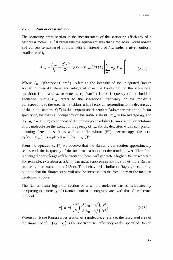
Chapter 2
47
2.2.6 Raman cross section
The scattering cross section is the measurement of the scattering efficiency of a
particular molecule.18 It represents the equivalent area that a molecule would absorb
and convert to scattered photons with an intensity of 𝐼𝑚𝑛 under a given uniform
irradiance of 𝐼0
𝜎𝑚𝑛 =
𝐼𝑚𝑛
𝐼0
=27𝜋5
32𝜈0(𝜈0 − 𝜈𝑚𝑛)3𝑔𝑓(𝑇) |∑ 𝛼𝜌𝜎(𝜈0)
𝜌𝜎
|
2
(2.27)
Where, 𝐼𝑚𝑛 ( photons/s ∙ cm2 ) refers to the intensity of the integrated Raman
scattering over 4𝜋 steradians integrated over the bandwidth of the vibrational
transition from state 𝑚 to state 𝑛 . 𝜈0 (cm−1) is the frequency of the incident
excitation, while 𝜈𝑚𝑛 refers to the vibrational frequency of the molecule
corresponding to the specific transition. 𝑔 is a factor corresponding to the degeneracy
of the initial state 𝑚. 𝑓(𝑇) is the temperature dependent Boltzmann weighting factor
specifying the thermal occupancy of the initial state 𝑚. 𝛼𝜌𝜎 is the average 𝜌𝑡ℎ and
𝜎𝑡ℎ (𝜌, 𝜎 = 𝑥, 𝑦, 𝑧) component of the Raman polarizability tensor over all orientations
of the molecule for the excitation frequency of 𝜈0. For the detection with a non-photon
counting detector, such as a Fourier Transform (FT) spectroscopy, the term
𝜈0(𝜈0 − 𝜈𝑚𝑛)3 is replaced with (𝜈0 − 𝜈𝑚𝑛)4.
From the equation (2.27) we observe that the Raman cross section approximately
scales with the frequency of the incident excitation to the fourth power. Therefore,
reducing the wavelength of the excitation beam will generate a higher Raman response.
For example, excitation at 532nm can induce approximately five times more Raman
scattering than excitation at 785nm. This behavior is similar to Rayleigh scattering,
but note that the fluorescence will also be increased as the frequency of the incident
excitation reduces.
The Raman scattering cross section of a sample molecule can be calculated by
comparing the intensity of a Raman band in an integrated area with that of a reference
molecule19
𝜎𝑅𝑆 = 𝜎𝑅
𝑟 (𝐼𝑆
𝐼𝑟) [
𝐸(𝜈0 − 𝜈𝑗𝑟)
𝐸(𝜈0 − 𝜈𝑗𝑆)
](𝑐𝑟
𝑐𝑆) (2.28)
Where 𝜎𝑅 is the Raman cross section of a molecule. 𝐼 refers to the integrated area of
the Raman band. 𝐸(𝜈0 − 𝜈𝑗) is the spectrometer efficiency at the specified Raman

Chapter 2 Introduction to Raman and Surface-Enhanced Raman Spectroscopy
48
shift frequency of 𝜈0 − 𝜈𝑗 . 𝑐 refers to the concentration of the sample molecule.
Superscripts 𝑟 and 𝑠 represent the reference and sample, respectively.
Table 2.3 A comparison of cross sections between different types of spectroscopy.
Transition of the spectroscopy Typical absolute cross section
Electronic (UV-VIS) absorption20 10-20 m2
Fluorescence21 10-20 m2
Vibrational (IR) absorption22 10-23 m2
Resonance Raman scattering23 10-29 m2
Non-resonant Raman scattering19,24 10-33 m2
Surface Enhanced Raman Scattering25 10-21 m2 to 10-27 m2
2.2.7 Pros and Cons of Raman spectroscopy
Raman spectroscopy is sensitive to molecules with homo-nuclear bonds. For example,
C-C, C=C and C≡C bonds can be easily distinguished by Raman spectroscopy.10 IR
spectroscopy, on the other hand, is sensitive to the vibrations of hetero-nuclear
functional groups and polar bonds, especially OH stretching. Fluorescence, however,
is only sensitive to the fluorescent bonds, such as Rhodamine B, Rhodamine 6G,
Dihydrorhodamine, Fluorescein, etc.
Raman spectroscopy can be applied to characterize bulky solids, granular solids, clear
and scattering solutions and gases. It requires little sample preparation, while the
fluorescent method has constraints on the labeling of samples, and the IR method is
limited to sample thickness, uniformity, dilution etc. However, Raman spectroscopy
is not applicable to metals and alloys and it becomes difficult to measure samples with
dark colors or high fluorescence. In Table 2.4 we have summarized the main features
and sample applicability of Raman, IR and fluorescence spectroscopy. Table 2.5
compares the sample applicability of different spectroscopy approaches.
Table 2.4 Features of Raman, Near-IR absorption and fluorescence spectroscopy.
Raman Near-IR absorption Fluorescence
Assignments Molecular
vibrations
Molecular vibrations &
rotations
Fluorescent bonds
Spectral band width Narrow Medium Wide
Intensity Low Low High
Source Laser Xenon arc lamp
Silicon Carbide/Silicon
Nitride emitter
Laser
LED
Mercury-vaper lamp
Labeling Label-free Label-free Labeling required

Chapter 2
49
Table 2.5 Sample applicability of Raman, IR absorption and fluorescence spectroscopy.26–28
Raman IR absorption Fluorescence
Sample applicability ★★★★✰ ★★★★★ ★✰✰✰✰
Sample preparation ★★★★★ ★★★✰✰ ★✰✰✰✰
Darkly colored sample ★✰✰✰✰ ★★★★✰ ★★★★★
Gas, Vaper ★★★✰✰ ★★★★★ ★★★✰✰
Aqueous solutions ★★★★★ ✰✰✰✰✰ ★★★★★
Clear Fluids ★★★★★ ★★★✰✰ ★★★★★
Scattering Fluids ★★★★★ ★★★✰✰ ★★★★✰
Granular Solids ★★★★★ ★✰✰✰✰ ★★★★★
Bulk Solids, Clear ★★★★★ ★★★★✰ ★★★★★
Bulk Solids, Scattering ★★★★★ ★✰✰✰✰ ★★★★★
(1=Poor 5=Excellent)
2.3 Instrumentation for Raman spectroscopy
The original Raman scattering was observed by utilizing the sun light or a mecury
lamp as excitation, and a few colored filters and photographic plates to record the
spectra for hours.29,30 Thanks to technological development, modern Raman
spectroscopic systems provide ways to obtain Raman spectra with tremendous higher
sensitivity and spectral resolution. In general, a Raman spectroscopy system consists
of a light source, an excitation optical path, a sample under test, a collection optical
path and a spectrometer, as shown in Figure 2.13. The optical paths are constructed
with several optical lenses, filters, mirrors, and other optical components.

Chapter 2 Introduction to Raman and Surface-Enhanced Raman Spectroscopy
50
Figure 2.13 Schematic of a dispersive Raman spectroscopy setup.31
2.3.1 Light source
Nowadays most of the Raman spectroscopy systems use lasers as excitation source
because of their high intensity, directionality and monochromatic properties. Table
2.6 lists some laser sources used for Raman detection.
Table 2.6 Typical lasers used in Raman spectroscopy.
Laser
wavelength
(nm)
Laser type Maxium
Power
Raman wavelengths
(nm)
Stokes region,
100~3000 cm-1
Comments
Near-IR
1064 Nd: YAG 3 W 1075~1563 FT spectrometer, risk
of sample thermal
degradation
830 Semi-conductor 300mW 827~980
785 Semi-conductor 500mW 791~1027 Most widely used
excitation source for
Raman spectroscopy
VIS
632.832,33 He-Ne 500mW 637~781 High Raman signal,
high fluorescence 532 Semi-conductor
or Nd: YAG
1.5W 535~632.8

Chapter 2
51
514.5 Argon 517~608 influence, risk of
sample degradation 405-510 Semi-conductor 1W 406~602
UV
213-400 Semi-conductor 1W 213~455 Resonance Raman
spectroscopy
According to equation (2.27) for the Raman cross section and the (𝜈0 − 𝜈𝑚𝑛)4
approximation, incident light with higher frequences will give rise to a higher Raman
response. However, an excitation with higher frequences will result in a higher
fluorescense that interferes with the Raman signal. Nowdays, most of the commercial
Raman spectroscopy setups are equiped with 785nm laser as excitation light to make
a trade-off between the intensity of the Raman signal and the influence of fluorescence.
2.3.2 Filters
As mentioned before, the intensity of Rayleigh scattering is dominant over Raman
scattering. Therefore, the use of a notch filter or long-pass optical filter at the end of
the collection path is usally necessary to reduce the Rayleigh scattering. In some
Raman spectroscopy systems, band-pass optical filters with a narrow full-width half-
maxium (FWHM) bandwidth are placed next to the exciation source to suppress the
ambient light as well as the secondary laser lines. Besides, a dichroic mirror or laser
line mirror with different reflection and transmission characteristics at two different
wavelengths is used to split the excitation and the collection path.
2.3.3 Lenses
The lenses in a conventional Raman spectroscopy system include an excitation lens
for focusing the laser onto the sample and collimating the scattered light emitted by
the sample after excitation, and a collection lens for collecting the Raman signal into
the entrance of the detector. Most of the Raman spectroscopy systems use objective
lenses with a large NA as excitation lenses in order to achieve a high excitation
efficiency. The main rule of thumb for selecting the collection lens is to match the
dimension and the NA of the detector’s entrance, such as the facets of the optical
fibers or the slit of the spectrometer.
2.3.4 Spectrometer
Raman scattering typically can be captured and detected by a dispersion-based or
Fourier Transform (FT) spectrometer.10 As the name suggests, a dispersion-based
spectrometer applies a stationary or dynamic dispersive element to generate spectra
of the incoming radiation. The typical stationary dispersive elements are refraction
prisms and diffraction gratings. The dynamic dispersive elements include acousto-

Chapter 2 Introduction to Raman and Surface-Enhanced Raman Spectroscopy
52
optic tunable filters (AOTF), liquid crystal tunable filters (LCTF), linear variable
filters (LVF) and circular linear variable filters (CLVF).34 Among these elements, the
diffraction grating is the most widely used in modern compact spectrometers in the
visible and NIR region with high spectral resolution and fast response. The dispersed
signal can be measured by a CCD or CMOS array.
A Fourier-transform spectrometer detects the spectra by modulating the radiation in
the time domain through interference and then Fourier-transforming the interferogram.
The Fourier-transform spectrometers with Germanium or InGaAs detectors have
overwhelming advantages over the dispersive spectrometers in the IR region because
of their wide spectral range, high throughput, signal-to-noise ratio and spectral
resolution.
2.4 Surface Enhanced Raman Spectroscopy (SERS)
2.4.1 History of SERS
Although Raman scattering is widely considered to have great advantages for the
study of vibrational and rotational modes of molecules, in the early days, the
advantages of Raman spectroscopy only stayed at the theoretical phase. From
discovery35 to practical applications, Raman spectroscopy was far from being
developed compared with other optical detection techniques, such as X-ray,
fluorescence and infrared spectroscopy. There are many reasons for this, but the key
point is that the Raman scattering intensity itself is very weak. As mentioned in the
previous sections, the intensity of Raman scattering is only one out of thousands to
millions of the Rayleigh scattering. The previous excitation sources used to observe
Raman scattering were usually mercury lamps with monochromatic and poor
directional energy and low intensity, which led to the slow progress of research in
Raman in the 30 years after 1928.36 In the 1960s, with the invention of lasers and the
development of computer technology, the study of Raman spectroscopy began to
accelerate. Especially in 1974, Fleischman et al. accidentally discovered that Pyridine
molecules adsorbed on the surface of electrochemically roughened silver electrodes
produced very strong Raman scattering.37 This phenomenon did not attract special
attention at the beginning but was understood as the roughening of the silver
electrodes resulted in an increase in total surface area, which adsorbed more Pyridine
molecules and led to the increase of the Raman scattering intensity. However, Van
Duyne et al. pointed out that the Raman signal can be enhanced to 106 times which
couldn’t simply be explained by the increment of the surface area.38 They believed
that there must be some connection between the surface properties and the Raman

Chapter 2
53
enhancement, which is now known as Surface Enhanced Raman Scattering. The
discovery of the SERS phenomenon not only greatly expanded the researchers’
perception of Raman scattering, but also brought new impetus to the development of
Raman spectroscopy. However, in the following decades, the use of Raman
spectroscopy in practical applications was still relatively low.39 One of the main
reasons is that SERS is a type of surface sensitive technology where sample molecules
need to be adsorbed on a specific surface but developing a reliable and stable SERS
substrate was quite challenging at that time. More importantly, the understanding of
SERS mechanisms had not been well explored.
Only until the 1990s, with the rapid development of nanotechnologies and
nanomaterials, and the emergence and extensive study of various SERS substrates,
Raman spectroscopy and SERS have been widely utilized in more and more
application domains. The theoretical research on Raman and SERS mechanisms have
also stepped into an entirely new stage.
With the generation and extensive study of various SERS substrates, Raman
spectroscopy and SERS have becoming popular not only in applications, but also in
theoretical research. The combination of SERS with micro/nano sensors has
enormously improved the accuracy, sensitivity and reliability of molecular
characterization both qualitatively and quantitatively.
There have been many assumptions and controversies regarding the mechanisms of
SERS, but nowadays, it is widely accepted that the dominant contributor to most of
the SERS phenomena is the electromagnetic enhancement mechanism. In addition,
the chemical mechanism also explains some of the SERS processes. According to the
equation for Raman response mentioned previously (equation (2.24)), the magnitude
of the induced dipole moment which characterizes the Raman scattering, is relevant
to the electric field E0 and the molecular polarizability. Among these two factors, the
electromagnetic enhancement mechanism corresponds to the local electric field, and
the chemical enhancement corresponds to the molecular polarizability respectively.

Chapter 2 Introduction to Raman and Surface-Enhanced Raman Spectroscopy
54
2.4.2 Electromagnetic Enhancement
Figure 2.14 (a) An Au nanoparticle acts as an antenna by excitation of a dipolar localized
surface plasmon resonance (LSPR).40 (b) FDTD simulated Electromagnetic field enhanced of
an Au nanoparticle due to the LSPR, excited by 785nm wavelength radiation.
Figure 2.14 depicts the electromagnetic enhancement schematically for the case of an
Au nanoparticle. The electromagnetic mechanism is the main enhancement effect of
the electromagnetic field amplification induced by resonance excitations based on
localized condition-electron oscillation on the surface of metallic nanostructures,
which is called surface plasmon (SP).41 This type of resonance, known as dipolar
localized surface plasmon resonance (LSPR), can be derived from the optical
extinction spectrum, including absorption and elastic scattering of specific metallic
nanostructures.16 The oscillation frequency 𝜔𝑚𝑎𝑥 of the plasmons in the metallic
structure depends on the dielectric function of the metal 휀𝑚𝑒𝑡𝑎𝑙(𝜔) and the
surrounding dielectric 휀𝑚(𝜔). The electromagnetic enhancement has two key features.
First of all, the coupling state of the photon and localized surface plasmons associate
with a sharp increase in the amplitude of the electromagnetic field near the rough
metallic surface. Therefore, the molecules adsorbed on the surface are subjected to
much stronger electromagnetic fields. In addition, the molecular dipole radiates
Raman scattering in close vicinity of metal rather than in free space.16 Virtually, not
only the incoming radiation from the excitation source, but also the Stokes Raman
scattering at a frequency of 𝜔𝑠 = 𝜔𝑖𝑛𝑐 − 𝜔𝑣𝑏 can induce LSPR of the metallic
nanostructure for a specific vibration mode. Both the local field enhancement and the
Raman radiation enhancement originating from the electromagnetic field can be
coupled into the metal substrate LSPR. Although the coupling may not be the same
for the two enhancements, the resonance should be at least similar in quality. The
overall intensity of SERS is given by Equation (2.29). It depends on the

Chapter 2
55
electromagnetic field of both the incident radiation 𝜔𝑖𝑛𝑐 and the induced Raman
scattering 𝜔𝑠
𝐼𝑆𝐸𝑅𝑆 = 𝐼𝑖𝑛𝑐(𝜔𝑖𝑛𝑐) ∙ 𝐼(𝜔𝑠) = |𝐸𝑖𝑛𝑐(𝜔𝑖𝑛𝑐)|2 ∙ |𝐸(𝜔𝑠)|2 (2.29)
Therefore, the optimal SERS enhancement requires that the incident EM radiation at
𝜔𝑖𝑛𝑐 and the Raman scattering radiate at 𝜔𝑠 are in resonance with the LSPR peak of
the nanostructure. In general, in order to fulfill the conditions for visible and NIR
excitation sources, it is necessary to utilize nanostructures with typical dimensions
between 20nm and 100nm. LSPR is strongly dependent on the size and shape of the
nanostructures. Due to the coupling from the interaction of LSPR of the individual
nanostructures, LSPR is also stronger for the nanostructures with smaller spaces. The
degree of enhancement by LSPR on the metallic nanostructures compared to
conventional Raman scattering is called the SERS enhancement factor (EF). For a
small metallic nanosphere, the electromagnetic enhancement factor can be explicitly
described as42,43
𝐸𝐹𝑒𝑚(𝜔𝑠) ≅ |
휀(𝜔𝑖𝑛𝑐) − 휀0
휀(𝜔𝑖𝑛𝑐) + 2휀0
|
2
|휀(𝜔𝑠) − 휀0
휀(𝜔𝑠 + 2휀0)|
2
(𝑟
𝑟 + 𝑑)12
(2.30)
Where, 휀(𝜔)is the dielectric function of the metal associated with its frequency, and
휀0 represents the dielectric constant of the surrounding medium. 𝑟 is the radius of the
nanosphere, and 𝑑 is the distance between the molecule and the surface. Index 𝑖𝑛𝑐
represents the incident light and 𝑠 stands for the scattered light. Noble metals such as
Au, Ag and Cu are the proper materials for SERS under the typical visible and NIR
excitation44, as the real part of 휀(𝜔) is close to −2휀0, and the imaginary part is small.
The enhanced local field of a 100nm diameter nanosphere with different base
materials according to the FDTD simulations are listed in Table 2.7. The real part
Re(휀) and imaginary part Im(휀) of the dielectric function of the materials at certain
wavelengths (𝜆) are extracted from the Lumerical FDTD database.
Table 2.7 Permittivity of some materials and maximum amplitude of the electromagnetic field
of a 100nm diameter nanosphere under 785nm excitation. (Lumerical FDTD database &
Simulation results)
Metal 𝜆 (nm) Re(휀) Im(휀) |E|/|E0|
Au 775 -20.787 0.729 4.15
Ag 756 -33.451 3.127 3.88
Pt 775 -15.808 26.716 3.59
Cu 729 -19.686 1.949 4.04
Al 775 -67.017 45.134 3.53

Chapter 2 Introduction to Raman and Surface-Enhanced Raman Spectroscopy
56
Fe 775 -3.96 21.6 3.45
Ni 775 -12.671 20.946 3.64
Ti 775 -3.3824 18.084 3.43
Si 785 13.726 0.0518 2.27
SiO2 707 2.117 0 1.47
(Re(ε): real part, and Im(ε): imaginary part of the dielectric function of the materials)
Figure 2.15 The normalized EF of a nanosphere drops fast down when the distance of the
molecule from the surface increases. The legends refer to the radius of the nanosphere.
According to equation (2.30), the electromagnetic enhancement factor also largely
depends on the radius of the nanosphere and the distance of the molecule from the
surface, as shown in Figure 2.15. The enhancement decreases fast as the distance of
the molecule from the surface becomes larger than 50nm for nanoparticles with a
radius smaller than 100nm. This implies that the sample molecule must be near the
metallic surface to induce the highest Raman scattering. Normally, a maximum
enhancement factor, or single molecule enhancement factor (SMEF) is defined to
characterize the optimal enhancement of the SERS substrate, which is given by the
|𝐸𝑙𝑜𝑐(𝜔𝑖𝑛𝑐)|4 approximation, since the shifted frequency of Raman scattering is not
far from that of the excitation16
𝑆𝑀𝐸𝐹(𝜔𝑖𝑛𝑐 , 𝜔𝑠) ≅|𝐸𝑙𝑜𝑐(𝜔𝑖𝑛𝑐)|2
|𝐸0(𝜔𝑖𝑛𝑐)|2
|𝐸𝑙𝑜𝑐(𝜔𝑖𝑛𝑐)|2
|𝐸𝑙𝑜𝑐(𝜔𝑠)|2
≅|𝐸𝑙𝑜𝑐(𝜔𝑖𝑛𝑐)|4
|𝐸0(𝜔𝑖𝑛𝑐)|4
(2.31)
The electromagnetic field tend to be enhanced more according to the localized surface
plasmon resonance in the area that is close to the sharp tips, edges, in the pitch area
between two nanostructures and other sub-structures on top of the smooth structure,
as illustrated in Figure 2.16.

Chapter 2
57
Figure 2.16 FDTD simulated electric fields of an Au nano-pyramid, cube and nanospheres in
an external EM radiation at 785nm wavelength.
2.4.3 Chemical Enhancement mechanism
The chemical enhancement mechanism refers to the Raman scattering enhanced by
the analyte molecules rather than the interaction of the incident radiation with SERS
substrates. The polarizability of the molecule binding on a noble-metal surface can be
changed owing to different transitions and processes45. This change can be induced
by either the charge transfer transition between the Fermi level of metal and the
highest occupied molecular orbital (HOMO) of sample molecules, or the charge
transfer transition between the valence band (VB) or conduction band (CB) of the
dielectric substrate and lowest unoccupied molecular orbital (LUMO) of analyte
molecules.42 In addition, the charge transfer transition between HOMO and LUMO or
between VB and CB of the substrate material is also helpful to the enhancement of
the Raman signal due to the resonance Raman scattering. These transitions and
processes can be understood as changes in the shape of the internal electron structures,
which leads to altering of the relative strength and frequencies of the molecular
vibrational modes, or even give rise to new vibrational modes. It is obvious that the

Chapter 2 Introduction to Raman and Surface-Enhanced Raman Spectroscopy
58
chemical enhancement has different effects on different molecular-substrate
combinations and each vibrational band within that molecule. The chemical
enhancement generally contributes to an additional enhancement factor of 10-100
accordingly.36
2.4.4 SERS substrates
The SERS phenomenon mainly originates from the electromagnetic enhancement
ascribed to the LSPR. Therefore, to perform a SERS experiment, it is essential to
choose or fabricate proper SERS substrates with an optimal LSPR effect and thus with
a high enhancement factor. The most critical aspects of a SERS substrate are the
shapes and dimensions of surface structures and the type of noble-metal that covers
or forms the surface structures. The typical SERS substrates include conventional
roughened electrodes, colloidal nanoparticles, metal island films and modern
periodical nanostructures.
Roughened electrodes
Electrochemically roughened silver electrodes were the initial type of SERS
substrates in history.37 In 1974, M. Fleischmann and his colleagues discovered that
Pyridine adsorbed on the electrode of an electrochemical cell generated an
enormously high intensity Raman signal. Their electrode was fabricated by the
electrochemical Oxidation-Reduction Cycle (ORC). The process of fabrication is to
put a polished silver plane in a cell and to apply a cyclic linear potential sweeping for
15 minutes. The formation and reduction of silver chloride during each cycle finally
resulted in a fully etched silver surface. The surface area of the silver plane by the
ORC process can be increased by at least a factor of 10. Some kinds of metal
electrodes, such as Cu, Al and Ni can also be easily roughened by chemical corrosion
to be used as SERS substrates.46 But these methods are problematic when treating
other noble metals such as Au, Pt and Rh, because they tend to generate a compact
oxide layer that hinders further dissolution and deposition of the surface.47 To
overcome this obstacle, A.J. Ariva and co-workers implemented a unique roughening
procedure such that a Pt electrode with a large surface area and controlled roughness
can be produced in acidic electrolytes due to the reduction of a previously generated
hydrous Pt oxide layer by applying a high-frequency periodic potential.48 The
roughening can also be realized by controlling the oxidation and a reduction of the
current rather than the potential. The typical surface protrusion of electrochemically
roughened surfaces is 25 to 500nm depending on the electrolyte, the metal and the
ORC potential or current.47 The enhancement factors of typical noble and transition
metal electrodes vary very much, ranging from 1 to 6 orders of magnitude, in terms

Chapter 2
59
of the surface morphology and the nature of the metal. Figure 2.17 shows the STM
image of a Pt electrode and the SEM image of a Rh electrode after an ORC procedure.
Figure 2.17 (Left) The Scanning Tunneling Microscope (STM) image of a Pt electrode
roughened by controlled a ORC potential, (Right) the AFM image of a Rh electrode
roughened by a controlled ORC current.47
Colloidal nanoparticles
Au and Ag nanoparticles in colloids are widely used as SERS substrates in chemical
and biological research.49 These colloidal nanoparticles can easily be synthesized via
chemical reaction without sophisticated lab equipment and processes. C. G.
Blatchford et al. developed a synthesis method for Au colloids by mixing a solution
of 0.27mM gold chloride acid and 17mM tri-sodium citrate solution with a volume
ratio of 19:1. It was rapidly mixed with vigorous stirring and then gentle stirring at
90°C for 40 minutes. The Au nanoparticles in the colloid fabricated by this approach
are between 12nm to 18nm.50 The dimension range of the Au nanoparticles can be
adapted by controlling for example the concentrations of the gold chloride acid and
the tri-sodium, the pH of the solvents, the reaction temperature and the stirring time,
resulting in an average diameter of more than 30nm.51 The synthesis of colloidal Ag
nanoparticles has been reported in many papers. Briefly, an ethylene glycol solution
of 0.25M AgNO3 and an ethylene glycol (EG) solution of 0.25M
Polyvinylpyrrolidone (PVP) were mixed with 1:6 volume ratio at room temperature.
The reaction was taking place at 160°C for 60 minutes with vigorous stirring and
resulted in colloidal Ag nanoparticles with diameters ranging from 100nm to 300nm.52
Adapting the molar ratio of AgNO3 and PVP close to 1:1 can even create Ag
nanowires and nanocubes.53 Silver triangular nanoplates can also be synthesized by
replacing the PVP solution with N,N-dimethylformamide (DMF) solution. In addition
to the chemical approaches, Ag nanoparticles can also be produced physically by a
granular-film approach.54

Chapter 2 Introduction to Raman and Surface-Enhanced Raman Spectroscopy
60
Figure 2.18 (A) SEM image of silver nanowires, (B) Transmission Electron Microscopy
(TEM) image of an individual Ag nanowire, (C) SEM image of silver triangular nanoplates,
(D) TEM image of silver triangular nanoplates, (E) SEM image of Ag nanoparticles, (F) TEM
image of Ag nanoparticles. 52
In recent years, some composite nanoparticles with multilayers and unconventional
shapes have been utilized as SERS substrates. Jin-Qun Xue and co-workers explored
surface-imprinted core-shell Au nanoparticles as a specific functional SERS
substrate.55 The two-layer nanoparticles were fabricated by a method based on a sol-
gel process where a 2nm thick molecularly imprinted polymer (MIP) layer was capped
on top of each Au core with a diameter of 50nm. The MIP material has shown high
affinity for the target molecules thus resulting in a stronger SERS signal than that of
the bare Au nanoparticles. I.I.S Lim and co-workers investigated Au and magnetic
nanoparticles coated with gold shells as bio-functional SERS nanoprobes. The
magnetic core could be either Fe2O3 or MnZn ferrite.56 The diameter of the core-shell
nanoparticles ranges from 30nm to 90nm depending on the conditions during
synthesis. Qiao An et al. developed the process for the fabrication of Ag nanoparticles
towards modified Fe3O4@carbon core-shell nanospheres as SERS probes for organic
pollutants detection.57 The size and shape of the core-shell nanospheres can be

Chapter 2
61
controlled by modifying the concentration of stock AgNO3 solution during the
synthesis.
Figure 2.19 TEM images of (A) AuNPs and (B) MIP-AuNPs.55
Figure 2.20 TEM images of Fe3O4@C@Ag nanospheres with different sizes.57
The enhancement factor of colloidal nanoparticles typically ranges from 104 to 109
accordingly.58–61
Metal island films
Metal island films on substrates are commonly used SERS substrates as they can be
fabricated in large areas at relatively low cost. Physical methods for the fabrication of
metal island films including vacuum thermal evaporation62 and sputtering coating63
are based on the self-assembly of the metal particles, as shown in Figure 2.21 and
Figure 2.22. The mass thicknesses of the metal island film and the dimensions of the
individual metal islands can be controlled by tuning the deposition speed of the
evaporation or sputtering process. Ag island films can also be deposited onto stainless
steel substrates by multiple scan cyclic voltammetry (CV) using an electrolyte
containing 0.1M KNO3, 0.1M KCN and 0.01M AgNO3 in a conventional three-
electrode cell.64 Adjusting the potential scan rate gives rise to Ag island films with
different thicknesses and dimensions.

Chapter 2 Introduction to Raman and Surface-Enhanced Raman Spectroscopy
62
Figure 2.21 Ag island films with mass thicknesses of 5nm, 10nm, 15nm and 20nm on
crystalline silicon substrates. Each image shows an area of 1µm × 1µm.62
Figure 2.22 SEM images of different Ag island films on a stainless steel substrate at potential
CV rates of 50mV/s, 100mV/s, 150mV/s and 200mV/s, respectively. 64 The scale bar is 1µm.
The analytical enhancement factor of electrochemically deposited Ag island films can
be as high as 3.7 × 10¹² corresponding to a detection limit of 5 × 10-16 M for R6G
according to the literature.64 But considering the affinity of the molecules with the
SERS substrate and taken into account that the molecules were distributed unevenly
at low concentration, an enhancement factor up to a 9th order of magnitude is
reasonable.
Periodical nanostructures / nanostructure arrays
The progress of modern nanotechnology and nanomaterial science has brought
enormous possibilities for the fabrication of SERS substrates with higher stability,
sensitivity and reproducibility. As suggested by the electromagnetic enhancement
mechanism, periodical nanostructures tend to produce higher and more homogeneous
LSPR compared to unevenly distributed nanostructures in space. The periodical
nanostructures can be fabricated by various approaches such as electrodeposition,
nanoimprinting lithography, e-beam lithography, chemical etching or a combination
of different approaches.
The self-assembly nature of the metal nanoparticles provides a relatively easy way of
fabricating periodical nanostructures. Hui Wang and co-workers reported a
specifically designed approach to deposit Au nanoshells into a 2D periodic array with
sub-10nm interparticle gaps65, as shown in Figure 2.23. The synthesized Au

Chapter 2
63
nanospheres were functionalized with surfactant cetyltrimethyl ammonium bromide
(CTAB) into colloidal nanoshells first. A droplet of this colloidal nanoshells were
placed on a substrate and dried, and finally organized into a hexagonal close packed
(hcp) pattern. Jian Feng Li et al. also reported self-assembled Au nanoparticles as
SERS substrates. But unlike the work of Hui Wang et al. where the Au nanoparticles
were covered with CTAB, Jian Feng Li isolated the Au nanoparticles with a transition
metal shell or silica shell.66
Figure 2.23 (a) Scheme of the nanoshell array fabrication and (b) SEM image of the nanoshell
array. 65
Wonjoo Lee reported self-assembled Au nanospheres with a controlled diameter and
spacing. The fabrication process involved solvent annealing, quaternization, colloid
adsorption and overgrowth, as shown in Figure 2.24.67
Figure 2.24 (a) AFM of the P4VP arrays, and SEM images of AuNP arrays on the quaternized
PS-b-P4VP films after overgrowth time of (b) 0 minutes, (c) 1 minute, (d) 3 minute. And (e)
the scheme of AuNP array fabrication. (i) Solvent annealing. (ii) Quaternization, (iii) Colloid
adsorption, (iv) Overgrowth. (Blue: substrate, green: P4VP, yellow: Polystyrene; red: Au). 67
Metal film over nanospheres (MFON), especially AgFON surfaces (Figure 2.25) are
very robust plasmonic materials for SERS detection.68,69 The procedure is to apply a

Chapter 2 Introduction to Raman and Surface-Enhanced Raman Spectroscopy
64
monolayer of self-assembled polystyrene or a SiO2 nanospheres mask on top of a
substrate, and then covered with a thin layer of noble metal via thermal evaporation
or sputtering. Polystyrene nanobeads and silica nanoparticles can be synthesized via
a half seeded emulsion polymerization method70 and Sol-Gel process respectively.71
The diameter of the nanospheres of the MFON are typically large (400-600nm), but
the atomic scale roughness behavior in combination with this large scale
nanostructures results in an enhancement factor up to 107.
Figure 2.25 SEM images of the AgFON SERS substrate from (A) side and (B) top-down.
J. Haes Amanda and co-workers combined the AgFON method based on self-
assembly of polystyrene nanobeads and nanolithography technique, and fabricated a
nano triangular array as SERS substrate (Figure 2.26).72 To produce the triangular
footprint, the nanospheres and the atomic Ag layer were removed by sonicating the
sample in a solvent. Nanospheres with a diameter of 400nm result in nanotriangles
with an in-plane width of 100nm and interparticle distance of 230nm approximately.
The enhancement factor of the periodical nanotriangles is up to 9 × 10⁷ characterized
by Raman scattering of benzenethiol.
Figure 2.26 (a) AFM image of the nanotriangle array; (b) Raman spectrum benzenethiol from
the nanotriangle arrays enhancement.72

Chapter 2
65
The above method can be further developed to fabricate close-packed arrays (CPA),
sparse arrays (SA), spheres removal (SR) structures on substrate or optical fibers as
SERS sensors,73,74 as shown in Figure 2.27.
Figure 2.27 SEM image of nanostructures on the fiber tip with (A) CPA, (B, C) SA, (D) CPA-
SR and (E) SA-SR patterns using 1µm diameter PS nanospheres. Scale bars are 3µm.73
H. Schneidewind and co-workers investigated Ag-covered polymer based
nanogratings as SERS substrates.75 A 70nm thick electro-sensitive resist layer was
spin coated on top of a quartz substrate and then polymerized by electron-beam
lithography into polymer nanogratings. An Al2O3 layer with a thickness of around
1nm was deposited and then covered with 20nm thick Ag film as effective metal for
SERS. The enhancement factor of this polymer-based SERS substrate is 4 orders of
magnitude.
Figure 2.28 (a) Scheme of the fabrication process of polymer-based nanogratings as SERS
substrate; (1) spin coating and E-beam lithography, (2) Atomic Layer Deposition (ALD), (3)
Sputtering. (b) SEM image of the nanogratings.

Chapter 2 Introduction to Raman and Surface-Enhanced Raman Spectroscopy
66
Applying nano-imprinting lithography with or without chemical etching can also give
rise to periodical nanostructures.76–78 The enhancement factors of the typical
nanopillar arrays are in the order of 104 to 106, as shown in Figure 2.29.
Figure 2.29 Nanopillar arrays fabricated by (a) nano-imprinting lithography76 and (b)
chemical etching.77
Two-photon polymerization (2PP) additive printing is a new technology suitable for
the fabrication of arbitrary 3D micro- and nano-structures. The typical spatial
resolution of the 2PP technique is between 150nm to 200nm, however minimum
feature sizes of 52nm can be realized under specific conditions.79 2PP 3D printed
nanostructures such as a nanocorral complex and nanocorral array80 and a
nanopyramid81 with Ag coating give rise to a SERS enhancement factor in the order
of 104 to 106.
Figure 2.30 SEM image of 2PP printed (a) nanocorral complex, (b) nanocorral array, and (c)
nanopyramid.
In Table 2.8 we have summarized the characteristics of different types of SERS
substrates including the enhancement factors, synthesis and fabrication methods and
typical dimensions.

Chapter 2
67
Table 2.8 Comparison of different types of SERS substrates.
SERS substrate EF/ log Synthesis / Fabrication dimensions
Roughened
electrodes46–48
1 - 6 Electrochemical ORC
Chemical etching
25 – 500nm (surface
protrusion)
Colloidal nanoparticles,
nanocore-shells50-61
4 - 9 Chemosynthesis 10 – 300nm
(diameter)
Metal island films62–64 2 - 12 Thermal evaporation,
Sputtering, Electrochemical deposition
5 - 20nm (thickness)
Periodical
nanostructures65-81
4 - 9 Lithography, Chemical etching, Chemical
deposition, Self-assembly deposition,
ALD, 2PP and etc.
10 – 500nm
(diameter, pitch)
2.5 A brief overview on Raman and SERS applications
In the past decades, the number of publications on topics such as Raman spectroscopy
and Surface Enhanced Raman spectroscopy have grown tremendously, as shown in
Figure 2.31. It is almost unfeasible to provide a comprehensive overview of the fields,
not even in the subfields of Raman and SERS for toxicity or single cell detection.
Nevertheless, it is instructive to get insight into the different applications of Raman
spectroscopy and SERS from various angles rather than specific domains.
Figure 2.31 Number of publications on Raman OR Surface Enhanced Raman spectroscopy
(SERS) per year from 1999 to 2019. (Statistic data extracted from the Web of Science,
accessed on April 7, 2020)

Chapter 2 Introduction to Raman and Surface-Enhanced Raman Spectroscopy
68
Table 2.9 Number of publications on Raman OR Surface Enhanced Raman spectroscopy
(SERS) from 1999 to 2019 categorized according to the fields of application. (Statistic data
extracted from the Web of Science, accessed on April 7, 2020)
Field: Web of Science Categories Record
Count
% of
245,817
MATERIALS SCIENCE MULTIDISCIPLINARY 66,683 27.127
CHEMISTRY PHYSICAL 51,069 20.775
PHYSICS APPLIED 50,893 20.704
PHYSICS CONDENSED MATTER 31,205 12.694
CHEMISTRY MULTIDISCIPLINARY 28,175 11.462
OPTICS 24,594 10.005
NANOSCIENCE NANOTECHNOLOGY 24,422 9.935
SPECTROSCOPY 16,090 6.546
PHYSICS ATOMIC MOLECULAR CHEMICAL 13,140 5.345
ENGINEERING ELECTRICAL ELECTRONIC 12,400 5.044
CHEMISTRY ANALYTICAL 11,262 4.581
MATERIALS SCIENCE COATINGS FILMS 10,199 4.149
ELECTROCHEMISTRY 7,691 3.129
PHYSICS MULTIDISCIPLINARY 7,479 3.043
ENGINEERING CHEMICAL 7,287 2.964
CHEMISTRY INORGANIC NUCLEAR 7,127 2.899
MATERIALS SCIENCE CERAMICS 6,252 2.543
INSTRUMENTS INSTRUMENTATION 5,875 2.39
ENERGY FUELS 5,509 2.241
POLYMER SCIENCE 5,444 2.215
METALLURGY METALLURGICAL
ENGINEERING
5,288 2.151
BIOCHEMISTRY MOLECULAR BIOLOGY 4,169 1.696
CRYSTALLOGRAPHY 3,955 1.609
MULTIDISCIPLINARY SCIENCES 3,733 1.519
CHEMISTRY APPLIED 3,606 1.467
Table 2.9 lists the application domains of Raman and SERS grouped in the Web of
Science Categories. More than 90% of the research output is in the field of chemistry,
materials science, physics and nano-science and technology. Conventional Raman and

Chapter 2
69
SERS Raman spectroscopy can be applied to characterize the structure of the materials
based on their fingerprint frequencies of specific chemical groups or measure the
concentration of certain analytes by analyzing the intensity of the Raman signal.
Raman and SERS spectroscopy are very useful tools for online monitoring the
progress of chemical reactions.82
In crystallography, single crystals can be detected by utilizing Raman spectroscopy
because Raman signals provide unique information about folding, substrate binding
and catalysis of the biomolecules.83 Gergely Katona and co-workers reveal the end-
on peroxide intermediates in a nonheme iron enzyme via Raman-assisted
crystallography.84 Bo Gong et al. detected the innersphere interactions between the
Phosphate backbone of the hepatitis delta virus (HDV) ribozyme and the magnesium
hydrate.85
The advantage of being label-free makes Raman spectroscopy a powerful tool for
toxin detection. Various types of mycotoxins, such as fumonisin, deoxynivalenol and
citrinin in maize, wheat, barley, corn or beverage can be identified by SERS.86–89 K.
Samir and co-workers also traced thiram pesticide residues from fruits by confocal
SERS spectroscopy.90 J. Hongquan and his co-worker investigated the feasibility of
antimicrobial characterization by a Ag nanoparticles based SERS approach.91
Confocal Raman spectroscopy is widely used in biological and medical research. With
the maturity of confocal Raman micro spectrometers (CRM), the field of single cell
investigation has been extended significantly. Intracellular contents, such as
DNA/RNA information from precisely defined positions in living or fixed cells can
be obtained.92,93 The chemical fingerprints of cells by Raman spectroscopy can be
used as evidence for cancer diagnositics.94–96
Raman spectroscopy is becoming an increasingly important analytical tool in the field
of art and archaeology. A. Sanchez et al. combined micro Raman spectroscopy and
X-ray microfluorescence to analyze the pigments in glass and ceramic vessel
fragments found in the Iberian cemetery Tutugi (4th-3rd century, BC).97 R. Wang and
L. Yuesheng investigated multi excitation Raman spectroscopy for identifying
Chinese jade.33 The study of pigments, dyes and binders in antique art paintings by
non-contacting Raman spectroscopy gave new indications of painting techniques in
ancient times.98
Out of the fields discussed here, there is no doubt that Raman spectroscopy and SERS
have been widely used in a lot of other application domains. There is also no doubt
that Raman and SERS will pave the way towards a lot of other applications in the
future.

Chapter 2 Introduction to Raman and Surface-Enhanced Raman Spectroscopy
70
References
1. Pérez‐Juste, I. & Faza, O. N. Interaction of radiation with matter. in Structure
Elucidation in Organic Chemistry: The Search for the Right Tools 1, 1–26
(Wiley, 2014).
2. Born, M. & Wolf, E. Principles of Optics: electromagnetic theory of
propagation, interference and diffraction of light. (Pergamon Press, 1970).
3. Sathyanarayana, D. N. Vibrational spectroscopy: theory and applications.
(New Age International, 2015).
4. Pieczonka, N. P. W. & Aroca, R. F. Inherent complexities of trace detection
by surface-enhanced Raman scattering. ChemPhysChem 6, 2473–2484 (2005).
5. Ikhdair, S. M. Rotation and vibration of diatomic molecule in the spatially-
dependent mass Schrodinger equation with generalized q -deformed Morse
potential. Chem. Phys. 361, 9–17 (2009).
6. Sage, M. L. Morse Oscillator Transition Probabilitles for Molecular Bond
Modes. Chem. Phys. 35, 375–380 (1978).
7. D.Louck, J. Derivation of the Molecular Vibration-Rotation Hamiltonian
from the Schrodinger Equation for the Molecular Model. J. Mol. Spectrosc.
61, 107–137 (1976).
8. Wang, W. & Paliwal, J. Vibrational Spectroscopy for Food Processing. in
Introduction to Advanced Food Process Engineering (ed. Sahu, J. K.) 497–
534 (CRC Press, 2014).
9. Meiselman, S., Cohen, O., DeCamp, M. F. & Lorenz., V. O. Measuring
vibrational coherence lifetimes in liquid methanol using transient coherent
Raman scattering Measuring. J. Phys. Conf. Ser. 497, 012004 (2014).
10. Khan, S. A. et al. Fourier Transform Infrared Spectroscopy: Fundamentals
and Application in Functional Groups and Nanomaterials Characterization. in
Handbook of Materials Characterization 317–344 (SPRINGER, 2018).
doi:https://doi.org/10.1007/978-3-319-92955-2_9
11. Robert, B. Resonance Raman spectroscopy. Photosynth. Res. 101, 147–155

Chapter 2
71
(2009).
12. Lacksberg, J. O. B., Lerstam, E. R. I. K. A., Aruyama, Y. U. K. I. M., Ochrane,
C. O. J. C. & Ossman, G. E. R. R. Miniaturized time-resolved Raman
spectrometer for planetary science based on a fast single photon avalanche
diode detector array. Appl. Opt. 55, 739–748 (2020).
13. Shipp, D. W., Sinjab, F. & Notingher, I. Raman spectroscopy: techniques and
applications in the life sciences. Adv. Opt. Photonics 9, 315 (2017).
14. Berg, E. R., Freeman, S. A., Green, D. D. & Ulness, D. J. Effects of Hydrogen
Bonding on the Ring Stretching Modes of Pyridine. J. Phys. Chem. 110,
13434–13446 (2006).
15. Lin-na, Z., Lin-Jie, H., Su-Hua, C. & Bo, C. Molecular vibrational
Spectroscopy and its Applications in Chemistry. Fujian Anal. Test. 4, 258–
275 (1995).
16. Prochazka, M. Basics of Surface-Enhanced Raman Scattering (SERS). in
Surface-Enhanced Raman Spectroscopy. Biological and Medical Physics,
Biomedical Engineering 21–59 (SPRINGER, 2015).
doi:https://doi.org/10.1007/978-3-319-23992-7_3
17. Musso, M. Raman Spectroscopy: Comparison of Infrared Spectra with those
gathered by Raman Spectroscopy of selected substances. (2000).
18. Meyer, S. A., Ru, E. C. Le & Etchegoin, P. G. Quantifying Resonant Raman
Cross Sections with SERS. J. Phys. Chem. 114, 5515–5519 (2010).
19. Wilcox, P. G., Emmons, E. D. & Pardoe, I. J. Raman Spectra and Cross
Sections of Chemical Warfare Agents, Agent Simulants, and Explosives Using
213nm Deep-Ultraviolet Laser Excitation. ARMY EDGEWOOD CHEMICAL
BIOLOGICAL CENTER APG MD ABERDEEN PROVING GROUND United
States (2018).
20. Volkamer, R., Spietz, P., Burrows, J. & Platt, U. High-resolution absorption
cross-section of glyoxal in the UV – vis and IR spectral ranges. J. Photochem.
Photobiol. A Chem. 172, 35–46 (2005).
21. Faris, G. W., Copeland, R. A., Mortelmans, K. & Bronk, B. V. Spectrally
resolved absolute fluorescence cross sections for bacillus spores. Appl. Opt.
36, 958–967 (1997).

Chapter 2 Introduction to Raman and Surface-Enhanced Raman Spectroscopy
72
22. Burkholder, J. B., Ravishankara, A. R. & Solomon, S. UV/visible and IR
absorption cross sections of BrONO2. J. Geophys. Res. 100, 16793–16800
(1995).
23. Johnson, C. R. & Asher, S. A. Wavelength dependence of the preresonance
Raman cross sections of CH3CN , Wavelength dependence of the
preresonance Raman cross sections of CH3CN ,. J. Chem. Phys. 82, 1985
(1985).
24. Aggarwal, R. L. et al. Measurement of the absolute Raman cross section of
the optical phonon in silicon. Solid State Commun. 151, 553–556 (2011).
25. Kneipp, K. et al. Single Molecule Detection Using Surface-Enhanced Raman
Scattering (SERS). Phys. Rev. Lett. 78, 1667–1670 (1997).
26. Doyle, W. M. & Stage, E. Comparison of Near-IR and Raman Analysis for
potential process applications. Tech. note AN-922, IFPAC-2001 1–20 (2001).
27. Mahadevan-Jansen, A. et al. Optical techniques for diagnosis of cervical
precancers: a comparison of Raman and fluorescence spectroscopies. in
Advances in Fluorescence Sensing Technology II 2388, 110–120 (1995).
28. Dieing, T., Hollricher, O. & Toporski, J. Confocal Raman Microscopy.
(SPRINGER, 2009).
29. Bhagavantam, S. The carbon isotope in Raman scattering. Part I. Proc. Indian
Acad. Sci. A 2, 86–92 (1935).
30. Pattabhiramayya, P. The study of the Raman effect in sodium nitrate. Proc.
Math. Sci. 7, 229–235 (1938).
31. Schmid, T. Raman Microspectroscopic Imaging of Binder Remnants in
Historical Mortars Reveals Processing Conditions. Heritage 2, 1662–1683
(2019).
32. Windom, B. C. & David, W. G. S. A Raman Spectroscopic Study of MoS2
and MoO3 : Applications to Tribological A Raman Spectroscopic Study of
MoS 2 and MoO 3 : Applications to Tribological Systems. Tribol. Lett. 42,
301–310 (2011).
33. Wang, R. Multiexcitation Raman Spectroscopy in Identification of Chinese
Jade. Spectrosc. Lett. 44, 432–439 (2011).
34. Ford, B. K., Volin, C. E., Murphy, S. M., Lynch, R. M. & Descour, M. R.

Chapter 2
73
Computed tomography-based spectral imaging for fluorescence microscopy.
Biophys. J. 80, 986–993 (2001).
35. Raman, C. V. A new radiation. India J. Phys 2, 387–398 (1928).
36. Mosier-Boss, P. Review of SERS Substrates for Chemical Sensing.
Nanomaterials 7, 142 (2017).
37. Fleischmann, M., Hendra, P. J. & McQuillan, A. J. Raman Spectra of Pyridine
Adsorbed at a Silver Electrode. Chem. Phys. Lett. 26, 163–166 (1974).
38. Duyne, V., P., R., L., D., Jeanmaire & Shriver., D. F. Mode-Locked Laser
Raman Spectroscopy-A New Technique for the Rejection of Interfering
Background Luminescence Signals. Anal. Chem. 46, 213–222 (1974).
39. Baia, M., Astilean, S. & Iliescu, T. Raman and SERS investigations of
pharmaceuticals. (SPRINGER, 2008). doi:10.1007/978-3-540-78283-4
40. Schlücker, S. Surface-enhanced raman spectroscopy: Concepts and chemical
applications. Angew. Chemie - Int. Ed. 53, 4756–4795 (2014).
41. Le Ru, E. C., Blackie, E. J., Meyer, M. & Etchegoin, P. G. Surface Enhanced
Raman Scattering Enhancement Factors: A Comprehensive Study. J. Phys.
Chem. C 111, 13794–13803 (2007).
42. Le Ru, E. & Etchegoin, P. Principles of Surfance Enhanced Raman
Spectroscopy and related plasmonic effets. Elsevier 1, (2009).
43. Pilot, R., Signorini, R., Durante, C. & Orian, L. A Review on Surface-
Enhanced Raman Scattering. Biosensors 9, 1–100 (2019).
44. Yang, X., Yang, M., Pang, B., Vara, M. & Xia, Y. Gold Nanomaterials at
Work in Biomedicine. Chem. Rev. 115, 10410–10488 (2015).
45. Kim, J. et al. Study of Chemical Enhancement Mechanism in Non-plasmonic
Surface Enhanced Raman Spectroscopy ( SERS ). Front. Chem. 7, 1–7 (2019).
46. Carron, K. T., Xue, G. & Lewis, M. L. A Surface Enhanced Raman
Spectroscopy Study of the Corrosion-Inhibiting Properties of Benzimidazole
and Benzotriazole on Copper. 7, 2–4 (1991).
47. Tian, Z., Ren, B. & Wu, D. Surface-Enhanced Raman Scattering: From Noble
to transition Metals and From Rough Surface to Ordered Nanostructures. J.
Phys. Chem. B 106, (2002).

Chapter 2 Introduction to Raman and Surface-Enhanced Raman Spectroscopy
74
48. Arvia, A. J., Salvarezza, R. C. & Triaca, W. E. The Development of Metal
overlays with smooth and rough topographies. Electrochim. Acta 34, 1051–
1071 (1989).
49. Wang, A. X. & Kong, X. Review of recent progress of plasmonic materials
and nano-structures for surface-enhanced raman scattering. Materials (Basel).
8, 3024–3052 (2015).
50. Blatchford, C. G. & Campbell, J. R. Plasma resonance - enhanced adsorbates
on gold colloids: aggregation c.g. blatchford,. Surf. Sci. 120, 435–455 (1982).
51. Dou, X., Jung, Y. M., Yamamoto, H., Doi, S. & Ozaki, Y. Near-Infrared
Excited Surface-Enhanced Raman Scattering of Biological Molecules on
Gold Colloid I: Effects of pH of the Solutions of Amino Acids and of Their
Polymerization. Appl. Spectrosc. 53, 133–138 (1999).
52. Zhang, J., Li, X., Sun, X. & Li, Y. Surface Enhanced Raman Scattering
Effects of Silver Colloids with Different Shapes. J. Phys. Chem. B 109,
12544–12548 (2005).
53. Banchelli, M. et al. Controlled Veiling of Silver Nanocubes with Graphene
Oxide for Improved Surface-Enhanced Raman Scattering Detection. ACS
Appl. Mater. Interfaces 8, 2628–2634 (2016).
54. Kawabata, S., Ishikawa, N., Mitsui, M. & Nakajima, A. Fabrication and
characterization of a granular film consisting of size-selected silver
nanoparticles : application to a SERS. Eur. Phys. J. D 158, 155–158 (2007).
55. Xue, J. Q., Li, D. W., Qu, L. L. & Long, Y. T. Surface-imprinted core-shell
Au nanoparticles for selective detection of bisphenol A based on surface-
enhanced Raman scattering. Anal. Chim. Acta 777, 57–62 (2013).
56. Lim, I. I. S. et al. Gold and magnetic oxide/gold core/shell nanoparticles as
bio-functional nanoprobes. Nanotechnology 19, 305102 (2008).
57. An, Q. et al. Silver-coated magnetite–carbon core–shell microspheres as
substrate-enhanced SERS probes for detection of trace persistent organic
pollutants. Nanoscale 4, 5210 (2012).
58. Knauer, M., Ivleva, N. P., Niessner, R. & Haisch, C. Optimized surface-
enhanced Raman scattering (SERS) colloids for the characterization of
microorganisms. Anal. Sci. 26, 761–766 (2010).

Chapter 2
75
59. Kuroda, K., Ishida, T. & Haruta, M. Reduction of 4-nitrophenol to 4-
aminophenol over Au nanoparticles deposited on PMMA. J. Mol. Catal. A
Chem. 298, 7–11 (2009).
60. Huang, T. & Xu, X.-H. N. Synthesis and characterization of tunable rainbow
colored colloidal silver nanoparticles using single-nanoparticle plasmonic
microscopy and spectroscopy. J. Mater. Chem. 20, 9867 (2010).
61. Lee, B. S., Lin, D. Z. & Yen, T. J. A low-cost, highly-stable surface enhanced
raman scattering substrate by si nanowire arrays decorated with au
nanoparticles and Au backplate. Sci. Rep. 7, 1–7 (2017).
62. Santbergen, R. et al. Application of plasmonic silver island films in thin-film
silicon solar cells. J. Opt. 14, (2012).
63. Mondt, R. De, Baert, K., Geuens, I., Vaeck, L. Van & Hubin, A. Study of the
Affinity of Thermographic Additives for Silver by Time-of-Flight Static
Secondary Ion Mass Spectrometry and Surface-Enhanced Raman
Spectroscopy on Silver Nanoparticles. Langmuir 22, 11360–11368 (2006).
64. Oriňáková, R. et al. Electrochemical deposition of SERS active
nanostructured silver films. Int. J. Electrochem. Sci. 8, 80–99 (2013).
65. Wang, H., Kundu, J. & Halas, N. J. Plasmonic nanoshell arrays combine
surface-enhanced vibrational spectroscopies on a single substrate. Angew.
Chemie - Int. Ed. 46, 9040–9044 (2007).
66. Li, J. F. & Tian, Z. Q. Shell-Isolated Nanoparticle-Enhanced Raman
Spectroscopy (SHINERS). Nature 464, 392–395 (2010).
67. Lee, W., Lee, S. Y., Briber, R. M. & Rabin, O. Self-assembled SERS
substrates with tunable surface plasmon resonances. Adv. Funct. Mater. 21,
3424–3429 (2011).
68. Dick, L. A., McFarland, A. D., Haynes, C. L. & Van Duyne, R. P. Metal film
over nanosphere (MFON) electrodes for surface-enhanced Raman
spectroscopy (SERS): Improvements in surface nanostructure stability and
suppression of irreversible loss. J. Phys. Chem. B 106, 853–860 (2002).
69. Masango, S. S. et al. High-Resolution Distance Dependence Study of Surface-
Enhanced Raman Scattering Enabled by Atomic Layer Deposition. Nano Lett.
16, 4251–4259 (2016).
Chapter 2 Introduction to Raman and Surface-Enhanced Raman Spectroscopy
76
70. Nuruzatulifah, A. M., Nizam, A. A. & Ain, N. M. N. Synthesis and
characterization of polystyrene nanoparticles with covalently attached
fluorescent dye. Mater. Today 3S, 112–119 (2016).
71. Rahman, I. A. & Padavettan, V. Synthesis of Silica Nanoparticles by Sol-Gel :
Size-Dependent Properties , Surface Modification , and Applications in
Silica-Polymer Nanocomposites — A Review. J. Nanomater. 2012, 1–15
(2012).
72. Haes, A. J., Haynes, C. L., Mcfarland, A. D. & Schatz, G. C. Plasmonic
materials for surface-enhanced sensing and spectroscopy. MRS Bull. 30, 368–
375 (2005).
73. Pisco, M. et al. Nanosphere lithography for advanced all fiber Sers probes.
Proc. SPIE 9916, 99161S–2 (2016).
74. Pisco, M. et al. Nanosphere lithography for optical fiber tip nanoprobes. Light
Sci. Appl. 6, e16229 (2017).
75. Schneidewind, H. et al. The effect of silver thickness on the enhancement of
polymer based SERS substrates. Nanotechnology 25, (2014).
76. Gartia, M. R. et al. Rigorous surface enhanced Raman spectral
characterization of large-area high-uniformity silver-coated tapered silica
nanopillar arrays. Nanotechnology 21, 395701 (2010).
77. Schmidt, M. S., Hübner, J. & Boisen, A. Large area fabrication of leaning
silicon nanopillars for Surface Enhanced Raman Spectroscopy. Adv. Mater.
24, OP11–OP18 (2012).
78. Schmidt, M. S., Boisen, A. & Jörg, H. Towards Easily Reproducible Nano-
structured SERS substrates. in IEEE Sensors Conference 1763–1767 (2009).
doi:10.1109/ICSENS.2009.5398468
79. Gan, Z., Cao, Y., Evans, R. A. & Gu, M. Three-dimensional deep sub-
diffraction optical beam lithography with 9 nm feature size. Nat. Commun. 4,
1–7 (2013).
80. Mu, J. et al. Direct laser writing of symmetry-broken nanocorrals and their
applications in SERS spectroscopy. Appl. Phys. B Lasers Opt. 117, 121–125
(2014).
81. Zhang, Q., Lee, Y. H., Phang, I. Y., Lee, C. K. & Ling, X. Y. Hierarchical 3D

Chapter 2
77
SERS substrates fabricated by integrating photolithographic microstructures
and self-assembly of silver nanoparticles. Small 10, 2703–2711 (2014).
82. Leung, S., Winkle, R. F., Wootton, R. C. R. & Andrew, J. A method for rapid
reaction optimisation in continuous-flow microfluidic reactors using online
Raman spectroscopic detection. Analyst 130, 46–51 (2005).
83. Gong, B. et al. Detection of Innersphere Interactions between Magnesium
Hydrate and the Phosphate Backbone of the HDV Ribozyme Using Raman
Crystallography. J. Am. Chem. Soc. 130, 9670–9672 (2008).
84. Katona, G. et al. Raman-Assisted Crystallography Reveals End-On Peroxide
Intermediates in a Nonheme Iron Enzyme. Science (80-. ). 316, 449–454
(2007).
85. Gong, B. et al. Detection of Innersphere Interactions between Magnesium
Hydrate and the Phosphate Backbone of the HDV Ribozyme Using Raman
Crystallography. Methods 49, 101–111 (2010).
86. Lee, K. & Herrman, T. J. Determination and Prediction of Fumonisin
Contamination in Maize by Surface – Enhanced Raman Spectroscopy
( SERS ). Food Bioprocess Technol 9, 588–603 (2016).
87. Lee, K., Herrman, T. J., Nansen, C. & Yun, U. Application of Raman
spectroscopy for qualitative and quantitative detection of fumonisins in
ground maize samples. IJRS 1, 1–14 (2013).
88. Yuan, J. et al. A rapid Raman detection of deoxynivalenol in agricultural
products. Food Chem. 221, 797–802 (2017).
89. Singh, D. K. et al. Detection of the mycotoxin citrinin using silver substrates
and Raman spectroscopy. J. Hazard. Mater. 265, 89–95 (2014).
90. Kumar, S., Goel, P. & Singh, J. P. Sensors and Actuators B : Chemical
Flexible and robust SERS active substrates for conformal rapid detection of
pesticide residues from fruits. Sensors Actuators B. Chem. 241, 577–583
(2017).
91. Jiang, H., Manolache, S., Wong, A. C. L. & Denes, F. S. Plasma-enhanced
deposition of silver nanoparticles onto polymer and metal surfaces for the
generation of antimicrobial characteristics. J. Appl. Polym. Sci. 93, 1411–
1422 (2004).

Chapter 2 Introduction to Raman and Surface-Enhanced Raman Spectroscopy
78
92. Puppels, G. J. et al. Laser irradiation and Raman spectroscopy of single living
cells and chromosomes: Sample degradation occurs with 514.5 nm but not
with 660 nm laser light. Exp. Cell Res. 195, 361–367 (1991).
93. Kudo, T., Wang, S. F., Yuyama, K. I. & Masuhara, H. Optical Trapping-
Formed Colloidal Assembly with Horns Extended to the Outside of a Focus
through Light Propagation. Nano Lett. 16, 3058–3062 (2016).
94. Agenant, M. et al. Clinical superficial Raman probe aimed for epithelial tumor
detection: Phantom model results. Biomed. Opt. Express 5, 1203 (2014).
95. Neugebauer, U. et al. Diagnostics of tumor cells by combination of Raman
spectroscopy and microfluidics. Clin. Biomed. Spectrosc. Imaging II 8087,
80870J (2011).
96. Pallaoro, A., Hoonejani, M. R., Braun, G. B., Meinhart, C. D. & Moskovits,
M. Rapid Identification by Surface-Enhanced Raman Spectroscopy of Cancer
Cells at Low Concentrations Flowing in a Microfluidic Channel. ACS Nano
9, 4328–4336 (2015).
97. Sánchez, A., Tuñón, J. & Parras, D. Micro Raman spectroscopy (MRS) and
energy dispersive x-ray micro fluorescence (µEDXRF) analysis of pigments
in the Iberian cemetery of Tutugi. J. Raman Spectrosc. 43, 1788–1795 (2012).
98. Bersani, D. & Madariaga, J. M. Applications of Raman spectroscopy in art
and archaeology. J. Raman Spectrosc. 43, 1523–1528 (2012).

Chapter 3
79
Chapter 3
3 Two-Photon Polymerized Nanostructures for
SERS Analysis
Surface Enhanced Raman Spectroscopy (SERS) is a surface sensitive detection
technique that can enhance the Raman scattering of molecules substantially due to the
oscillation of localized surface plasmons by using rough metal surfaces or
nanostructures. Nowadays, SERS has been employed in a variety of application
domains. The enhancement of Raman scattering makes SERS a powerful tool for
chemists to analyse the vibrational and rotational modes of single molecules1,2. SERS
has also been increasingly utilized in biological research and life sciences such as
cancer diagnostics3–5, DNA/RNA identification6–8, toxin and drug detection9–11. To
achieve these detection goals, SERS substrates with specific surface profiles having a
boosted electromagnetic field under laser excitation should be considered.
Electrochemically roughened metal electrodes have been used as SERS substrate
since 1974, but the low level of enhancement and lack of reproducibility has restricted
their applications12. Noble metal nanospheres ranging from 10-200nm in colloids or
as deposition are typical SERS substrates which can be synthesized by chemical
approaches13–15. Other kinds of irregularly shaped nanoparticles, such as nano-rod,
nano-triangles, nano-cubes, nano-stars, nano-cookies and core-shells are increasingly
investigated as SERS substrates since they can generate stronger plasmonic oscillation
due to the sharp tips or edges, therefore resulting in higher Raman enhancement16–21.
However, the repeatability and reproducibility of SERS measurements with
This chapter is based on a published article:
Liu, Q.; Vanmol, K.; Lycke, S.; Van Erps, J.; Vandenabeele, P.; Thienpont, H.; Ottevaere, H.
SERS using two-photon polymerized nanostructures for mycotoxin detection. RSC
Advances 2020, 10, 14274.

Chapter 3 Two-Photon Polymerized Nanostructures for SERS Analysis
80
nanoparticles can hardly be guaranteed because of the inhomogeneity of the particles’
distributions and shapes. Therefore, nano-pillar arrays, hemisphere arrays, triangle
arrays, and other periodical nanostructures have been developed as SERS substrates
by means of electrodeposition9 and nanoimprinting lithography22,23 to improve the
repeatability and reproducibility. However, these methods are time consuming and
less flexible. To fabricate these periodic nanostructures with different dimensions,
new polymer or silicon masks must be produced in advance. Chemical/plasma etching
provides a fast approach for large area SERS substrates manufacturing24,25, but only
nano-pillar arrays can be fabricated with this method.
In this chapter we present an additive manufacturing method employing two-photon
polymerization to fabricate periodic nanostructures as SERS sensing platform.
Multiple nano-pillar arrays with different dimensions are printed and characterized.
This approach allows fast and flexible prototyping of SERS substrates26,27. The use of
two-photon polymerization lithography can also greatly reduce the complexity and
lead time of the nanostructure manufacturing for SERS applications by computer-
aided design (CAD) and computer-aided manufacturing (CAM). We simulate the
boosting of electromagnetic fields for different nano-pillar arrays by the Finite-
Difference Time-Domain (FDTD) method.28 The simulation output is compared with
experimental results of Rhodamine B (RhB) solutions. In a proof-of-concept
experiment, we performed SERS measurements on a mix of Fumonisin b1 and
Deoxynivalenol. The spectra of these two types of mycotoxins are analysed with PCA
methods and with respect to their vibrational modes.
3.1 Fabrication of nanostructures with two-photon
polymerization and simulations
3.1.1 Two-photon polymerization process
Two-photon polymerization lithography is a novel 3D additive fabrication technique
based on two-photon absorption of photo resins29. When an ultrashort laser pulse is
highly focused onto the photoresist, it will initiate two-photon polymerization via two-
photon absorption in a small region where the energy is higher than a threshold. This
region is the so called ‘voxel’ which represents the minimum feature size we can
achieve by two-photon polymerization lithography. Typically, the voxel is defined as
an ellipsoid with a specified diameter and aspect ratio which are determined by
parameters such as the physical and chemical properties of the photoresist, the
intensity and illumination time of the femtosecond laser, the magnification and

Chapter 3
81
numerical aperture of the objective lens for focusing. The typical resolution of two-
photon polymerization is between 150nm to 200nm, but a resolution of 52nm can be
realized under certain circumstances with a newly developed photoresin with high
mechanical strength30. By moving the relative spatial position of the voxel with a
galvanometric mirror scanner and piezo stages, periodic or complex 3D structures can
be printed31.
Figure 3.1 Scheme of the two-photon polymerization system we used for manufacturing
nanostructures. (AOM: acousto-optical modulator).
In our process, we employ the Nanoscribe Photonic Professional GT 3D printer to
fabricate our SERS substrates. Figure 3.1 shows the schematic diagram of the GT 3D
printer. The GT printer has a 780nm wavelength femtosecond laser with about 100 fs
pulses. The minimum XY feature size we can achieve with the Nanoscribe GT with
IP-dip photoresin is about 200nm. The typical printing range is 300 × 300 µm2, and
the accessible writing area can be up to 100 × 100 mm2 using stitching. The 3D
printing of an individual nano-pillar array with an area of 50µm × 50µm takes 3 to 5
minutes. The fabrication process can be divided into three steps. First, we use CAD
software to design the nanostructures with nominal shapes, such as the ideal nano-
pillar arrays. These designs can be exported as general stereolithography (STL) files
and be imported to the workstation of the Nanoscribe GT. Next, according to the
system parameters of the 3D printer, such as the magnification of the objective lens,
the type of photoresin and the dimensions of the voxel, the workstation compiles the
STL files into CNC programs which contain the instructions and parameters the
printer will follow. The workstation runs the CNC programs virtually to simulate the
two-photon polymerization process. Finally, the Nanoscribe GT runs the CNC
programs such that the 3D nanostructures are fabricated. We use a 50× objective lens

Chapter 3 Two-Photon Polymerized Nanostructures for SERS Analysis
82
and IP-dip photoresin (Nanoscribe, Eggenstein-Leopoldshafen/BW, Germany) for the
two-photon polymerization manufacturing of the nanostructures.
3.1.2 Electromagnetic field enhancement simulation of nanostructures with
FDTD method
As explained in Chapter 2, it is generally accepted that the enhancement of SERS
stems from two major mechanisms, namely chemical and electromagnetic
enhancement.32 Chemical enhancement corresponds to the intrinsic properties of the
molecule adsorbed on the metallic surface, including the chemical polarity,
chemisorption, orientation with respect to the surface, etc33. The chemical mechanism
is explained only in specific occasions with low Raman enhancement contribution,
and it occurs jointly with the electromagnetic enhancement which is much more
dominant34.
According to the electromagnetic enhancement hypothesis, the interaction of incident
light with the metallic surface of a SERS substrate will generate oscillations of
localized plasma dipoles, thereby boosting the electromagnetic field in the region near
the surface35. The boosted region is interpreted as a ‘hotspot’ of the SERS substrate.
The electromagnetic enhancement factor, or single-molecule enhancement factor
(SMEF) for a molecule located at the hotspot can be expressed in the |𝐸𝑅|2|𝐸𝑆|2
approximation36 as discussed in equation (2.31):
𝑆𝑀𝐸𝐹(𝜔𝑅 , 𝜔𝑆) ≅|𝐸𝑙𝑜𝑐(𝜔𝑅)|2|𝐸𝑙𝑜𝑐(𝜔𝑅)|2
|𝐸0(𝜔𝑅)|2|𝐸𝑙𝑜𝑐(𝜔𝑆)|2 (3.1)
Where 𝜔𝑅 is the frequency of incident light, and 𝜔𝑆 is the Stokes frequency of Raman
radiation enhanced by the local field. 𝐸0 refers to the field of incident light, and 𝐸𝑙𝑜𝑐
refers to the local field induced by the incident light, respectively.
Normally, the Stokes frequency 𝜔𝑆 is quite close to the incident frequency 𝜔𝑅. The
expression can be further simplified to:
𝑆𝑀𝐸𝐹 ≅|𝐸𝑙𝑜𝑐(𝜔𝑅)|4
|𝐸0(𝜔𝑅)|4 (3.2)
This implies that the SMEF is proportional to the 4th power of the local field, which
provides a simple estimation to mimic the SERS performance via a numerical
approach. In this PhD we verify the feasibility of two-photon polymerized SERS
substrates both theoretically with the FDTD method using Lumerical software and
experimentally with Rhodamine B detection.

Chapter 3
83
The key parameters of the nano-pillar arrays are the height (H) and diameter (D) of
each pillar, and the pitch (P) between them, as shown in Figure 3.2. In a preliminary
study, nanopillar arrays with an aspect ratio of 1, i.e. having identical values of height
and diameter, are considered for a range from 200nm to 600nm by taking into account
the ~200nm resolution of two-photon polymerization. We built three different
simulation models and investigate them for their FDTD electromagnetic solutions,
whereby each model corresponds to one step of the nanostructure manufacturing
process. The first nominal shape model consists of cylindrical pillars, whereas the
second is a voxel-based model, in line with the 3D printing process flow of two-
photon polymerization manufacturing, and the third model reflecting the true
fabricated shape as measured by Veeco Dimension 3100 Atomic Force Microscopy
(AFM). FDTD solves Maxwell’s equations in the time domain by calculating the
electromagnetic field values changes at discrete steps (grid or mesh) in time28. We
started the FDTD simulations from 2D models, which ran very fast (<1 minutes) with
Lumerical software. Later we built 3D models of the nanostructures and performed in
depth simulations to assess the Raman enhancement performances, which took a
much longer time for each model as the operand increased exponentially with the
amount of meshes defined in the simulation. For example, the FDTD simulation for
the 200nm pillar array took several minutes, but the 600nm pillar array took several
hours.
Figure 3.2(a) and Figure 3.3(a) are illustrations of nano-pillar arrays for the nominal
shape model and the voxel-based model, respectively. Figure 3.2.(b, c, d) show the
induced electric field |𝐸|/|𝐸0| with 200nm, 400nm and 600nm nano-pillar arrays in
the nominal shape model under 785nm excitation after FDTD simulations. Figure
3.3.(b, c, d) show the induced electric field |𝐸|/|𝐸0| with 200nm, 400nm and 600nm
nano-pillar arrays in the voxel-based model under 785nm excitation after FDTD
simulations. Here 𝐸0 is the amplitude of the excitation electric field, and 𝐸 is the
amplitude of the induced electric field. In the nominal shape model, the leading
enhancement of the electric field appears in the edge of the nanostructures. Basically,
such perfect shapes are difficult to obtain via two-photon polymerization. In contrast,
we notice that the voxel-based model gives rise to complex discrete shapes with
cavities and bulges on top of a smoother profile. These complex structures induce
extended hotspot sections and higher electric field values in general. But it should be
mentioned that the complex structures may also destruct the enhancement in some
local areas which we will discuss later. The maximum electric field of the 200nm
pillar array in both the nominal shape model and the voxel-based model is larger than
the ones of the 400nm and 600nm pillar-arrays, suggesting that the 200nm pillar array
has a higher SMEF according to our FDTD simulations.

Chapter 3 Two-Photon Polymerized Nanostructures for SERS Analysis
84
Figure 3.2. (a) Drawing of a nominal shape model, and (b, c, d) electric field distribution of
the 200nm, 400nm and 600nm pillar arrays using the nominal shape model and simulated by
the FDTD method.

Chapter 3
85
Figure 3.3. (a) Drawing of a voxel-based model, and (b, c, d) electric field distribution of the
200nm, 400nm and 600nm pillar arrays using voxel-based model and simulated by the FDTD
method.
After two-photon polymerization fabrication, we employ a 20nm thick Au layer with
a sputtering coater such that the front surfaces as well as the sides of the nano-pillars
are covered with metal where localized enhancement can be induced by excitation.
The fabricated nano-pillar arrays are characterized with Scanning Electron
Microscopy (SEM) and Atomic Force Microscopy (AFM). Some of the nano-pillar
arrays are shown in Figure 3.4. Each of the periodic nanostructure arrays has an
effective area of 50µm×50µm and a 1µm thick base layer to increase the adhesion to
the silica glass and its stability. The silica glass has been silanized with 3-
(Trimethoxysilyl)propyl methacrylate before two-photon polymerization to further
improve the adhesiveness. The periodic lines visible in both the SEM and AFM
images are due to a stitching process that was used during the 3D fabrication to reduce
the size of the STL files. This effect should not deteriorate the SERS signal in the
experiments as the detection area is within the center area of each block, but will be
avoided by systematic optimization of the two-photon polymerization process in
future work.
Figure 3.4. Morphologies of 200nm, 400nm and 600nm nano-pillar arrays. Measured with
SEM (column 1 and 2) and AFM (column 3).
We obtained the morphological characteristics of the nano-pillar arrays based on an
analysis of SEM images and AFM data, shown in Table 3.1. The measured values of

Chapter 3 Two-Photon Polymerized Nanostructures for SERS Analysis
86
height, diameter and pitch are in good agreement with the designed values. Although
the homogeneity of the 200nm nano-pillar array looks visually less than the ones of
the 400nm and 600nm nano-pillar arrays, the standard errors of the height, diameter
and pitch of the different nanostructures caused by the fabrication errors are similar
according to the SEM and AFM measurements. We also notice that, although the
heights of the 200nm and 300nm structures are still within the confidence interval of
the measurements, they are a little bit smaller than the nominal values. This is
probably due to the limit of the AFM probe which cannot reach the bottom of the
trough when the pitch is very narrow. We build the fabricated shape model based on
the 3D data obtained from the AFM.
Table 3.1 Dimensions of nano-pillar arrays measured with SEM and AFM. (all units in nm)
Pillar/nm Height Diameter Pitch
200 179.7 ± 50.5 217.3 ± 38.1 228.8 ± 36.1
300 275.3 ± 54.5 287.5 ± 21.8 304.5 ± 22.4
400 431.1 ± 76.9 381.9 ± 35.2 358.0 ± 32.0
500 564.4 ± 67.6 474.0 ± 43.0 473.0 ± 46.6
600 625.0 ± 96.2 579.4 ± 35.2 573.1 ± 32.3
(The average and standard deviation for each pillar array are obtained over the measurements
within a 20µm by 20µm area.)
We performed the FDTD simulation on the fabricated shape model and investigated
its electromagnetic enhancement. Figure 3.5 illustrates the fabricated shape model and
the simulated electric field of one cross-section of 200nm, 400 and 600nm nano-pillar
arrays. Unlike the other two models in which the periodic pattern and induced hotspots
are homogeneously distributed, the fabricated model shows a poorer uniformity of the
hotspots because the oscillation of localized plasmonic dipoles is much more intricate
due to fabrication errors. In this case, the location of molecular adsorption and the
detection area are of great importance from a practical point of view. For instance, if
a molecule is adsorbed on the region of the middle pillar in Figure 3.5.(c), a stronger
Raman scattering will be induced compared to the other regions.

Chapter 3
87
Figure 3.5 (a) Drawing of a nominal shape model, and (b, c, d) electric field distribution of the
200nm, 400nm and 600nm pillar arrays using the fabricated model and simulated by the
FDTD method.
3.1.3 Influence of fabrication errors
During the actual fabrication process, displacement of voxel tracks and distortion of
the voxel shape is inevitable due to mechanical vibrations and the accuracy of the
printing device, fluctuation of the femtosecond laser power, a change of
environmental temperature, etc. To understand the influence of fabrication errors, we
performed FDTD simulations considering changes of pitch, height and diameter
values of the nano-pillar array, as shown in Figure 3.6. For a 400nm pillar array, a
pitch of 50nm less (b) than the original design (a) will increase the amplitude of the
electric field from 7 to 7.5, whereas 100nm less pitch (c) will increase the amplitude
of the electric field to 9.6. As a result, according to the |𝐸𝑙𝑜𝑐(𝜔𝑅)|4 approximation,
the SMEF for 400nm pillar array with 50nm and 100nm displacement in pitch are 1.3
times and 3.5 times more than that of the original, respectively. The errors in the height
of the pillar will also change the distribution and intensity of the electric field (d, e
and f). If there is a displacement between two adjacent layers in the fabrication
process, the diameters of the pillars will be different than our expectation. In some
cases, the electric field pattern is similar to that of the pitch errors (g and h), while in
other cases the distribution of hotspots is totally relocated from the troughs to the top

Chapter 3 Two-Photon Polymerized Nanostructures for SERS Analysis
88
areas (i). The simulation results indicate that the SMEF of the nano-pillar arrays is
more sensitive to horizontal fabrication errors than to vertical errors.
Figure 3.6. Electric fields of 400nm pillar array in voxel-based model without (a) and with
fabrication errors (b-i). 50nm and 100nm closer pitch (b, c) increase the electric field. 50nm
height error (d) and 100nm height error (e) of one pillar, and all pillars with 50nm height error
(f) have little impact on the electric field. Diameter errors due to displacement of different
adjacent layers (g-i) have big impact to the relocation and intensity change of electric fields,
as these also reduce the pitch values.
In addition to the errors of the macro profile, the substructures such as nano-cavities,
bulges or spikes on top of the nanostructures may result in much more complex
enhancement patterns.

Chapter 3
89
3.2 Experiments with the printed SERS substrates
3.2.1 SERS enhancement analysis
To experimentally verify the enhancement factors of the two-photon polymerized
SERS substrates, we prepared 10µM Rhodamine B solutions in ethanol and water
respectively and performed Raman measurements utilizing a confocal Raman
microscope (Bruker Optics - Senterra). This spectrometer is equipped with a 785nm
laser which is the same wavelength as has been used in our FDTD simulations. The
experimental enhancement factor, or the analytical enhancement factor (AEF) can be
calculated according to the following equation36:
𝐴𝐸𝐹 = (𝐼𝑆𝐸𝑅𝑆/𝑁𝑆𝐸𝑅𝑆)/(𝐼𝑅𝑒𝑓/𝑁𝑅𝑒𝑓) (3.3)
Where 𝐼𝑆𝐸𝑅𝑆 and 𝐼𝑅𝑒𝑓 are the intensities of the SERS signal and conventional Raman
signal respectively. 𝑁𝑆𝐸𝑅𝑆 stands for the number of molecules that induce a SERS
signal, and 𝑁𝑅𝑒𝑓 is the number of molecules that generate normal Raman scattering.
Figure 3.7. (a) Raman background of the 200nm pillar array; (b) Average Raman spectra of
10µM RhB obtained with 200nm pillar arrays. Baselines are corrected by subtracting the
background Raman signal. Spectra are obtained under a 785nm wavelength and 2.5mW laser
excitation with 1 second integration time. The dashed lines refer to the upper and lower range
of the spectra. Average spectrum is obtained over 16 measurements.
We obtained the background spectrum of the 200nm pillar array for a reference, as
shown in Figure 3.7(a). Next, we placed 30µL of the Rhodamine B ethanol solution
on the SERS substrates, and measured the Raman spectra in the dry state under a
2.5mW excitation with a 50× objective lens. The sample deposited area (glass plate)
is much larger than the SERS sensitive area (50µm by 50µm) and the SERS sensitive
area is in the middle of the base plate where the concentration of the molecule under
test is lower compared to the ring but more uniform. We can estimate 𝑁𝑆𝐸𝑅𝑆 with
reference to the laser spot size and deposition area under the assumption that the

Chapter 3 Two-Photon Polymerized Nanostructures for SERS Analysis
90
Rhodamine B molecules are evenly delivered on the overall SERS substrate. The
reference measurements are conducted by analyzing the Raman scattering of a
Rhodamine B aqueous solution since water gives very weak Raman background. We
calculated the 𝑁𝑅𝑒𝑓 inside the interaction probe volume of the 50× objective lens
under the same excitation. However, we must be aware that the local AEF with
inhomogeneous distribution of the molecules may be different than the overall AEF
of the SERS substrate, which may be influenced by parameters such as the uniformity
of the nano-pillar array, the adsorption of the molecules and the surface tension of the
SERS substrate. Figure 3.7(b) shows the SERS spectra of Rhodamine B on a 200nm
nano-pillar array after subtracting the background of the SERS substrate. Rhodamine
B molecules present distinct enhancement features at 629cm-1, 1203cm-1, 1287cm-1,
1363cm-1, 1511cm-1 and 1600cm-1. The peaks of the Rhodamine B’s spectra
correspond to the molecular vibrational modes as listed in Table 3.2.
Table 3.2 The intensities and peak assignments of main Raman bands of Rhodamine B.
Literature37–39 Raman (cm-1) SERS (cm-1) Assignment
619 S 622.5 S 629.5 S ν (Aromatic C-C)
965-980 W 978 W 969 W δ (Ethylene C-H)
1065-1085 W 1080 M 1086 M δ (Aromatic C-H)
1130 W 1115 W 1126 W δ (Aromatic C-H)
1199 M 1198 S 1203 S δ (Aromatic C-H)
1284 S 1281 S 1287 S δ (C-C)
1360 S 1359 S 1363 S ν (Aromatic C-C)
1508 S 1508 S 1511 S ν (Aromatic C-C)
1591 W 1595 W 1600 S ν (C=C)
1644 S 1647 S 1652 W ν (Aromatic C-C)
(ν: stretching, δ: deformation; W: weak; M: medium; S: strong)
The Raman peak of Rhodamine B at 1363cm-1 shows the highest intensity. Therefore,
we calculate the AEF corresponding to the 𝐼𝑆𝐸𝑅𝑆 and 𝐼𝑅𝑒𝑓 at 1363cm-1. Figure 3.8 is
the comparison of enhancement factors for the three different models obtained by
FDTD simulations and the experimental results. A maximum enhancement factor
close to 104 is achieved by our 200nm nano-pillar array. It is reasonable that smaller
structures give rise to a higher enhancement as they can induce stronger oscillation of
localized surface plasmons. The voxel-based model shows the best consistency with
experimental results. However, one interesting phenomenon we can observe is that
the experimental EFs are larger than the simulated EFs except for the 200nm and
300nm voxel-based models. This can be explained by the relocation and intensity
changes of hotspots due to the fabrication errors mentioned before. It is hard to predict
the precise influence of the fabrication errors over the entire SERS substrate, but we

Chapter 3
91
believe that the FDTD simulation of the fabricated shape model can give rise to a
better reflection of SERS performance if an AFM with higher resolutions and smaller
probe size can be used. In addition, because the major boosted electric field of them
is generated in the edge area, the EFs of the 300nm to 600nm nano-pillar arrays in the
nominal shape model show less differences.
Figure 3.8. Comparison of enhancement factors for the different models obtained by FDTD
simulations and the experimental result. The average and standard deviation of each
enhancement factor are obtained over 16 measurements on a different detection area of a
nano-pillar array.
Figure 3.9. Comparison of 10µM RhB Raman spectra on different substrates and the Raman
spectrum of pure RhB.
We also performed benchmark measurements of Rhodamine B with two types of
commercial SERS substrates from Silmeco (Copenhagen, Denmark) and Horiba, Ltd
(Kyoto, Japan) respectively, see Figure 3.9. The enhancement factor of our 200nm
pillar array is two orders of magnitude less than the 106 EF of Silmeco, which can be
proven by the spectra. It’s noteworthy that our SERS substrate is comparable with

Chapter 3 Two-Photon Polymerized Nanostructures for SERS Analysis
92
Horiba’s substrate and performs even better with a higher sensitivity. Therefore, our
two-photon polymerized SERS substrate can be used as a powerful tool to study the
vibrational modes of molecules.
Additionally, other types of periodic nanostructures, including nano-hemisphere
arrays and nano-grids have been printed by two-photon polymerization as well, as
shown in Figure 3.10. But the Raman performance of these SERS substrates is less
than that of the nano-pillar arrays both in simulations and experiments. Therefore, in
our later experiments we utilize only the 200nm pillar arrays.
Figure 3.10. SEM images of 200nm, 400nm and 600nm hemisphere arrays (a-c) and nano-
grids with 200nm, 400nm and 600nm spacing (d-f).
3.2.2 SERS substrate calibration
In order to further evaluate the performance of our two-photon polymerized SERS
substrates, we measured the Raman spectra of Rhodamine B with different
concentrations from 0.5µM to 1000µM. The calibration curves of the peak intensity
with respect to the concentration are shown in Figure 3.11(a). The peak intensity rises
as the concentration increases, but the rate of increment gradually falls off. From a
certain threshold of concentration (~750µM), the peak stops increasing and starts to
decrease. Because the SERS effective area is just within a few hundred nanometers,
the number of hotspots is limited. The molecules can quickly fill the hotspots of the
SERS substrate and emit enhanced Raman scattering under low concentrations.
However, as the concentration increases, the number of remaining hot spots begins to
decrease with the accumulation of molecules on the metallic surface. And eventually
a thick layer is formed that prevents the SERS signal underneath. This can be proved
by the microscope images of the original SERS substrate and the SERS substrate with
1mM Rhodamine B deposition in Figure 3.11(b, c).

Chapter 3
93
Figure 3.11. Calibration curves of the 200nm nano-pillar array showing the peak intensities at
629cm-1, 1287cm-1 and 1363cm-1 with respect to the RhB concentrations (a). Molecules can
easily adsorb on the SERS substrate in the low concentration condition (b), but a thick layer
of molecules with high concentration will restrain the SERS signal (c). The RhB molecules
cover both the nanostructures and the surrounding flat surfaces, for which the interaction of
molecules with nanostructures has changed the color of the RhB from red violet to green
under white light illumination due to a higher reflectivity at the green light band.
The detection limit of our 200nm pillar array for Rhodamine B is estimated to be
0.55µM (5.7 ppm) according to the linear regression of the calibration curve in the
low concentration region40.
3.3 An application of two-photon polymerized SERS substrates
3.3.1 Mycotoxin detection with 2PP polymerized SERS substrates
SERS is an ideal technique for biochemistry and toxicology because of its low laser
intensity, short integration time and small sampling volume required. As proof of
concept for our two-photon polymerized SERS substrate, we tested two types of
mycotoxins, Deoxynivalenol (DON) and Fumonisin b1 (FUM). Deoxynivalenol, also
known as vomitoxin, is a metabolite of fusarium graminearum which can cause
anorexic effects on humans41. Fumonisin is a metabolite of fusarium verticillioides,
one of the most prevalent seed-borne fungi associated with maize42. Long-term intake
of Fumonisin contaminated food can greatly increase the risk of esophageal cancer.
According to the EU’s Mycotoxins Factsheet43, the limit of deoxynivalenol in
unprocessed cereals is 1.25ppm, and the limit of Fumonisin in unprocessed maize is
4ppm. We measured the Raman spectra of 1ppm deoxynivalenol and 1.25ppm

Chapter 3 Two-Photon Polymerized Nanostructures for SERS Analysis
94
Fumonisin b1 in acetonitrile with the same equipment under the same excitation as
for Rhodamine B. The average spectra of Fumonisin b1 and Deoxynivalenol obtained
with our 200nm pillar arrays are shown in Figure 3.12.
Figure 3.12. Raman spectra of 1ppm DON and 1.25ppm FUM obtained with our 200nm pillar
array SERS substrate under a 785nm wavelength and 2.5mW laser excitation with 1 second
integration time. The concentrations of mycotoxins are close to the detection limit of our
SERS substrates and therefore it is difficult to recognize the mycotoxins directly.
3.3.2 Principal Component Analysis (PCA) for the spectra of mycotoxins
The concentrations of mycotoxins are close to the detection limit of our SERS
substrates. Therefore, it is difficult to recognize the DON and FUM directly by
comparing the spectra, although there are some distinguishing peaks present, such as
the 1452cm-1 and 1140cm-1 peaks of the DON spectrum, and the 873cm-1 and 1775cm-
1 peaks of the FUM spectrum respectively. We employed Principal Component
Analysis (PCA) towards a set of Raman spectra observed to discriminate them44. PCA
is one of the most common methods of multivariate analysis for classification
purposes which uses the spectral decomposition of a correlation coefficient. After
PCA transformation, we find that the first three principal components represent 85.9%
of the variance, and the two mycotoxins can be clearly distinguished by the second
and third principal components, as shown in Figure 3.13 (a). Raman spectra of DON
and FUM show good repeatability with groups of replies, which allow to detect
sensible between-sample differences.

Chapter 3
95
Figure 3.13. (a) Spectra of DON and FUM are clustered by the scores of the second and third
principal components. (b)-(c) Coefficients of principal components 1-3 which represent
85.9% of the variance.
By analyzing the coefficients of the second and third principal components which contains
fingerprint Raman shifts information of the two mycotoxins, as shown in Figure 3.13 (b),
combined with literature results, we obtained the characteristic peaks of the two mycotoxins
and the corresponding assignments, see Table 3.3.
Table 3.3 The characteristic peaks and assignments of main Raman bands of FUM and DON
according to PCA.
Mycotoxin Literature45–47 (cm-1) SERS (cm-1) assignment
FUM 760 754 ν (C-C)
868 873 ν (C-O-C)
1460 1466 δ (-CH3)
1488 1482 δ (C-H)
1776 1775 ν (C=O)
DON 780 787 ν (O-H) + ν (C-H)
855 852 ν (C-H)
923 927 ν (-CH3) + ν (C-H)
1139 1140 ν (C-H)
1293 1287 ν (C-H)
1430 1435 δ (C=C) + ν (-CH3) + ν (C-H)
1449 1452 ν (-CH3)
(ν: stretching, δ: deformation)

Chapter 3 Two-Photon Polymerized Nanostructures for SERS Analysis
96
3.4 Conclusions
We designed and fabricated a series of nano-pillar arrays as SERS substrates ranging
from 200nm to 600nm by using two-photon polymerization and gold sputtering. To
verify the feasibility of these nano-arrays as SERS substrates, we setup a nominal
shape model, a voxel-based model, and simulated the induced electric field under
785nm excitation alongside the nanostructures with the FDTD method. We
characterized the morphologies of the different nano-pillar arrays from a
comprehensive analysis of SEM images and AFM 3D data. The fabricated shape
model based on AFM data is defined as input for the FDTD simulations to determine
the induced electric field. The single molecule enhancement factor (SMEF) of
different models are calculated based upon the FDTD results.
We estimated the experimental enhancement factor (AFE) by analyzing the Raman
scattering of 10µM Rhodamine B solutions in ethanol and water. A maximum
enhancement factor closes to 104 is achieved with the 200nm pillar array. Benchmark
measurements have shown that obtained results of our two-photon polymerized SERS
substrates are comparable with the ones obtained with the commercial SERS
substrates. We compared the experimental enhancement factor with the SMEFs
obtained using different models for FDTD simulations, finding that the voxel-based
model gives the best consistency with the experimental results. In addition, we
analyzed the reasons for the differences between simulations and experiments.
Moreover, we evaluated the detection limit of the 200nm nano-pillar array SERS
substrates using different concentrations of Rhodamine B solutions and found the
limit to be 0.55µM. To demonstrate the proof-of-concept of our SERS substrates in
an application, we detected the Raman spectra of 1ppm deoxynivalenol and 1.25ppm
fumonisin b1 solutions. The two types of mycotoxin are discriminated by principal
component analysis (PCA). Our two-photon polymerized nano-pillar arrays pave the
way for fast prototyping of SERS substrates for biochemical and toxicological
research.
The limitation of two-photon polymerization is the restricted structure-sizes of the
nano-pillar arrays. But the enhancement factor of the SERS substrates can still be
increased by optimizing the nanostructures. Increasing the homogeneity of the
nanostructures should be further investigated with respect to parameters such as the
optimization of femtosecond laser power fluctuations, the photoresins and the voxel
path compiling. Finally, the quantitative analysis capabilities of our 2PP printed SERS
substrates should in future be investigated using other analytes such as crystal violet
(CV), p-mercaptobenzoic acid (p-MBA), 1,2-bis (4-pyridyl)-ethylene (BPE) and
biological samples.

Chapter 3
97
References
1. Michaels, A. M., Nirmal, M. & Brus, L. E. Surface enhanced Raman
spectroscopy of individual rhodamine 6G molecules on large Ag nanocrystals.
J. Am. Chem. Soc. 121, 9932–9939 (1999).
2. Le Ru, E. C., Meyer, M. & Etchegoin, P. G. Proof of single-mokeule
sensitivity in surface enhanced Raman scattering (SERS) by means of a two-
analyte technique. J. Phys. Chem. B 110, 1944–1948 (2006).
3. Lee, S. et al. Rapid and sensitive phenotypic marker detection on breast
cancer cells using surface-enhanced Raman scattering (SERS) imaging.
Biosens. Bioelectron. 51, 238–243 (2014).
4. Chon, H., Lee, S., Son, S. W., Oh, C. H. & Choo, J. Highly sensitive
immunoassay of lung cancer marker carcinoembryonic antigen using surface-
enhanced raman scattering of hollow gold nanospheres. Anal. Chem. 81,
3029–3034 (2009).
5. Sha, M. Y., Xu, H., Natan, M. J. & Cromer, R. Surface-Enhanced Raman
Scattering Tags for Rapid and Homogeneous Detection of Circulating Tumor
Cells in the Presence of Human Whole Blood. J. Am. Chem. Soc. 130, 17214–
17215 (2008).
6. Song, H., Lee, S., Kang, T. & Kim, K. Silver nanoislands based SERS-active
substrates for DNAs detection. Prog. Biomed. Opt. Imaging - Proc. SPIE
9340, (2015).
7. Kang, T., Yoo, S. M., Yoon, I., Lee, S. Y. & Kim, B. Patterned Multiplex
Pathogen DNA Detection by Au Particle-on-Wire SERS Sensor. Nano Lett.
10, 1189–1193 (2010).
8. Bell, S. E. J. & Sirimuthu, N. M. S. Surface-Enhanced Raman Spectroscopy
( SERS ) for Sub-Micromolar Detection of DNA / RNA Mononucleotides. J.
Am. Chem. Soc. 128, 15580–15581 (2006).
9. Zhou, Y., Chen, J., Zhang, L. & Yang, L. Multifunctional TiO2-coated Ag
nanowire arrays as recyclable SERS substrates for the detection of organic
pollutants. Eur. J. Inorg. Chem. 2012, 3176–3182 (2012).
10. Aoki, P. H., Furini, L. N., Alessio, P., Aliaga, A. E. & Constantino., C. J.
Surface-enhanced Raman scattering ( SERS ) applied to cancer diagnosis and
detection of pesticides , explosives , and drugs. Rev. Anal. Chem. 32, 55–76
(2013).

Chapter 3 Two-Photon Polymerized Nanostructures for SERS Analysis
98
11. Li, J. F. & Tian, Z. Q. Shell-Isolated Nanoparticle-Enhanced Raman
Spectroscopy (SHINERS). Nature 464, 392–395 (2010).
12. Fleischmann, M., Hendra, P. J. & McQuillan, A. J. Raman Spectra of Pyridine
Adsorbed at a Silver Electrode. Chem. Phys. Lett. 26, 163–166 (1974).
13. Dou, X., Jung, Y. M., Cao, Z. Q. & Ozaki, Y. Surface-enhanced Raman
scattering of biological molecules on metal colloid II: Effects of aggregation
of gold colloid and comparison of effects of pH of glycine solutions between
gold and silver colloids. Appl. Spectrosc. 53, 1440–1447 (1999).
14. Knauer, M., Ivleva, N. P., Niessner, R. & Haisch, C. Optimized surface-
enhanced Raman scattering (SERS) colloids for the characterization of
microorganisms. Anal. Sci. 26, 761–766 (2010).
15. Dou, X., Jung, Y. M., Yamamoto, H., Doi, S. & Ozaki, Y. Near-Infrared
Excited Surface-Enhanced Raman Scattering of Biological Molecules on
Gold Colloid I: Effects of pH of the Solutions of Amino Acids and of Their
Polymerization. Appl. Spectrosc. 53, 133–138 (1999).
16. Huang, T. & Xu, X.-H. N. Synthesis and characterization of tunable rainbow
colored colloidal silver nanoparticles using single-nanoparticle plasmonic
microscopy and spectroscopy. J. Mater. Chem. 20, 9867 (2010).
17. Guo, H., Xing, B., Hamlet, L. C., Chica, A. & He, L. Surface-enhanced
Raman scattering detection of silver nanoparticles in environmental and
biological samples. Sci. Total Environ. 554–555, 246–252 (2016).
18. Reznickova, A., Novotna, Z., Kasalkova, N. S. & Svorcik, V. Gold
nanoparticles deposited on glass: Physicochemical characterization and
cytocompatibility. Nanoscale Res. Lett. 8, 1–8 (2013).
19. Zhang, Z., Liao, F., Ma, S., Gao, S. & Shao, M. SERS and FDTD simulation
of gold nanoparticles grafted on germanium wafer via galvanic displacement.
Surf. Interface Anal. 47, 398–402 (2015).
20. Rodrıiguez-Lorenzo, L. et al. Intracellular mapping with SERS-encoded gold
nanostars. Integr. Biol. 3, 922–926 (2011).
21. An, Q. et al. Silver-coated magnetite–carbon core–shell microspheres as
substrate-enhanced SERS probes for detection of trace persistent organic
pollutants. Nanoscale 4, 5210 (2012).
22. Wang, H., Lai, K., Lin, Y., Lin, C. & He, J. Periodic Si Nanopillar Arrays
Fabricated by Colloidal Lithography and Catalytic Etching for Broadband and

Chapter 3
99
Omnidirectional Elimination of Fresnel Reflection. Langmuir 26, 12855–
12858 (2010).
23. Kuo, C., Shiu, J., Cho, Y. & Chen, P. Fabrication of Large-Area Periodic
Nanopillar Arrays for Nanoimprint Lithography Using Polymer Colloid
Masks. Adv. Mater. 13, 1065–1068 (2003).
24. Schmidt, M. S., Boisen, A. & Jörg, H. Towards Easily Reproducible Nano-
structured SERS substrates. in IEEE Sensors Conference 1763–1767 (2009).
doi:10.1109/ICSENS.2009.5398468
25. Schmidt, M. S., Hübner, J. & Boisen, A. Large area fabrication of leaning
silicon nanopillars for Surface Enhanced Raman Spectroscopy. Adv. Mater.
24, OP11–OP18 (2012).
26. Mu, J. et al. Direct laser writing of symmetry-broken nanocorrals and their
applications in SERS spectroscopy. Appl. Phys. B Lasers Opt. 117, 121–125
(2014).
27. Zhang, Q., Lee, Y. H., Phang, I. Y., Lee, C. K. & Ling, X. Y. Hierarchical 3D
SERS substrates fabricated by integrating photolithographic microstructures
and self-assembly of silver nanoparticles. Small 10, 2703–2711 (2014).
28. Zhou, Q. et al. A Surface-Enhanced Raman Scattering Sensor Integrated with
Battery-Controlled Fluidic Device for Capture and Detection of Trace Small
Molecules. Sci. Rep. 5, 12865 (2015).
29. Cumpston, B. H. et al. Two-photon polymerization initiators for three-
dimensional optical data storage and microfabrication. Nature 398, 51–54
(1999).
30. Gan, Z., Cao, Y., Evans, R. A. & Gu, M. Three-dimensional deep sub-
diffraction optical beam lithography with 9 nm feature size. Nat. Commun. 4,
1–7 (2013).
31. Obata, K., El-tamer, A., Koch, L., Hinze, U. & Chichkov, B. N. High-aspect
3D two-photon polymerization structuring with widened objective working
range ( WOW-2PP ). Light Sci. Appl. 12, 8–11 (2013).
32. Maher, R. C., Cohen, L. F., Le Ru, E. C. & Etchegoin, P. G. On the
experimental estimation of surface enhanced raman scattering (SERS) cross
sections by vibrational pumping. J. Phys. Chem. B 110, 19469–19478 (2006).
33. Davies, R. A., Chong, N. S. & Ooi, B. G. Chemical Enhancement of the
Surface Enhanced Raman Scattering Signals of Anilines via Their Ortho-

Chapter 3 Two-Photon Polymerized Nanostructures for SERS Analysis
100
Substituents. Opt. Photonics J. 03, 13–23 (2013).
34. Lombardi, J. R., Birke, R. L., Lu, T. & Xu., J. Charge-transfer theory of
surface enhanced Raman spectroscopy : Herzberg-Teller contributions. J.
Chem. Phys. 84, 4174 (1986).
35. Creighton, J. A. Surface raman electromagnetic enhancement factors for
molecules at the surface of small isolated metal spheres: The determination of
adsorbate orientation from sers relative intensities. Surf. Sci. 124, 209–219
(1983).
36. Le Ru, E. C., Blackie, E. J., Meyer, M. & Etchegoin, P. G. Surface Enhanced
Raman Scattering Enhancement Factors: A Comprehensive Study. J. Phys.
Chem. C 111, 13794–13803 (2007).
37. Zhang, J., Li, X., Sun, X. & Li, Y. Surface Enhanced Raman Scattering
Effects of Silver Colloids with Different Shapes. J. Phys. Chem. B 109,
12544–12548 (2005).
38. Luo, Z., Fang, Y. & Yao, J. A New Approach for Non-destructive Detection
of Dye Molecules by Combination of Terahertz Time-domain Spectra and
Raman Spectra. Trends Appl. Sci. Res. 2, 295–303 (2007).
39. Bio-Rad. KnowItAll ® AnalyzeIt MVP. (2019). Available at: http://www.bio-
rad.com/webroot/web/pdf/spectroscopy/global/english/literature/docs/95392
-Bio-Rad_KnowItAll_Software_AnalyzeIt_MVP_PCA_Datasheet.pdf.
40. Shrivastava, A. & Gupta, V. B. Methods for the determination of limit of
detection and limit of quantitation of the analytical methods. Chronicles
young Sci. 2, 21–25 (2011).
41. Pestka, J. J. & Smolinski, A. T. Deoxynivalenol : Toxicology and Potential
Effects on Humans. J. Toxicol. Environ. Health 8, 39–69 (2015).
42. Marasas, W. F. O. Discovery and Occurrence of the Fumonisins : A Historical
Perspective. Environ. Health Perspect. 109, 239–243 (2001).
43. Lerda, D. Mycotoxins Factsheet. (European Union, 2011).
44. Emge, D. et al. Bacillus Spore Classification via Surface-Enhanced Raman
Spectroscopy and Principal Component Analysis. Appl. Spectrosc. 62, 267–
272 (2008).
45. Lee, K. & Herrman, T. J. Determination and Prediction of Fumonisin
Contamination in Maize by Surface – Enhanced Raman Spectroscopy

Chapter 3
101
( SERS ). Food Bioprocess Technol 9, 588–603 (2016).
46. Lee, K., Herrman, T. J., Nansen, C. & Yun, U. Application of Raman
spectroscopy for qualitative and quantitative detection of fumonisins in
ground maize samples. IJRS 1, 1–14 (2013).
47. Yuan, J. et al. A rapid Raman detection of deoxynivalenol in agricultural
products. Food Chem. 221, 797–802 (2017).

Chapter 3 Two-Photon Polymerized Nanostructures for SERS Analysis
102

Chapter 4
103
Chapter 4
4 Integrated Confocal Raman Probe Combined with a
Freeform Reflector Embedded Lab-on-Chip
4.1 Introduction to a freeform reflector-based confocal Raman
spectroscopy lab-on-chip system
Miniaturized optical components, such as lenses, filters, optical fibers and mirrors can
be integrated to a microfluidic Raman lab-on-chip device to increase the excitation
and collecting efficiencies.1–4 Diane De Coster, a former PhD student in our research
group has developed a freeform reflector-based confocal Raman spectroscopy lab-on-
chip system for material characterization.4 As discussed in Chapter 1, one of the
objectives in this PhD is to further miniaturize this Raman spectroscopy experimental
setup and to enhance the Raman signal. To start with, this section gives an overview
of the confocal Raman spectroscopy lab-on-chip system developed by Diane De
Coster.
Part of this chapter has been submitted as:
Liu, Q., Barbieri, G., Thienpont, H., Ottevaere, H. (2017). Integrated confocal Raman probe
combined with a free-form reflector based lab-on-chip. In Optical System Alignment,
Tolerancing, and Verification XI (Vol. 10377). [1037706] SPIE. DOI: 10.1117/12.2274936
Liu, Q., De Coster, D., Loterie, D., Van Erps, J. A., Vervaeke, M., Missinne, J., Ottevaere, H.
(2016). Proof-of-concept demonstration of free-form optics enhanced confocal Raman
spectroscopy in combination with optofluidic lab-on-chip. In Micro-Optics 2016 (Vol. 9888).
[UNSP 98880E] SPIE. DOI: 10.1117/12.2227386
De Coster, D., Liu, Q., Vervaeke, M., Van Erps, J.A., Missine, J., Thienpont, H., Ottevaere, H.
(2017). Optofluidic chip for single-beam optical trapping of particles enabling confocal Raman
measurements. IEEE J. Sel. Top. Quantum Electron., 23(2), [5500109].

Chapter 4 Integrated Confocal Raman Probe Combined with a Freeform Reflector Embedded Lab-on-Chip
104
4.1.1 Confocal principle
Confocal microscopes are widely used in biological research for studying cell
structures as they can provide background-free images with high resolution by
rejecting the out-of-focus light. Typically, in a confocal system, a pinhole is placed at
the image plane of the lens, as shown in Figure 4.1. Light emitted from a source in the
focal plane can be focused by the lens to a spot and collected inside the pinhole. The
out-of-focus emissions will be strongly attenuated or rejected by the pinhole.
Therefore, a confocal system can suppress the background signals from the out-of-
focus regions to increase the quality of the wanted signal for a sample under test.
Figure 4.1 Illustration of confocal principle.4
4.1.2 Design of the confocal Raman spectroscopy LoC setup
The confocal Raman spectroscopy setup Diane De Coster has developed consists of a
freeform reflector embedded LoC and external optics for microfluidic measurements4,
as shown in Figure 4.2. The LoC on the bottom of the setup consists of three PMMA
layers. The 200µm thick bottom PMMA layer is embedded with a freeform reflector
coated with a reflective gold layer. The diameter and sag of the reflector are 1.684mm
and 300µm respectively. The 500µm thick middle layer consists of a 500µm width
fluidic channel and a chamber with a diameter slightly bigger than that of the reflector.
The focal point of the reflector is located in the center of the fluidic chamber, and
50µm above the bottom of the channel layer. The 500µm thick top layer is the sealing
layer for the fluidic channel. All the three layers are bonded together by UV curing
adhesive. The LoC enables a very high numerical aperture with aqueous flow filled
inside the chamber (NA=1.28) and allows a high collection efficiency of the Raman
scattering.
In this setup, the freeform reflector in the LoC and the collection lens work together
as the lens, and the core facet of the collection fiber works as the pinhole during the
confocal measurement, respectively. The confocal Raman spectroscopy setup consists
of an excitation and a collection path. In the excitation path, a 785nm wavelength laser
coming out of the single-mode fiber is collimated and reshaped by a set of lenses (L1)

Chapter 4
105
to a light beam of which its diameter is in line with that of the freeform reflector. The
collimated beam is then reflected by a laser line mirror to the LoC, and focused by the
freeform reflector to the focal point inside the fluidic chamber. The Raman scattering
will be induced where the laser light excites the sample under test due to the
vibrational modes of the molecules of the analytes in the flow. In the collection path,
the scattered Raman signal collimated by the freeform reflector passing through the
laser line mirror can be collected into the multi-mode collection fiber by the collection
lens (L2). A notch filter is placed in front of the collection lens to attenuate the
Rayleigh scattering of the laser light. The light bundle of the Raman scattering
originating from out-of-focus sources cannot pass through the fiber facet because of
the confocal principle. In this case, the Raman scattering of the out-of-focus regions,
especially from the polymer layers will be suppressed significantly.
Figure 4.2 (Left) schematic of the confocal Raman spectroscopy setup with a freeform
reflector embedded LoC. (Right) Geometrical parameters of the LoC.4
The shape of the freeform reflector is a derivation of a parabolic mirror by taking into
account the refractive transition between the polymer layer and the fluids inside the
chamber according to Fermat’s principle. The surface profile of the freeform reflector
is calculated by a numerical approach. The calculated shape is then introduced in the
Advanced Systems Analysis Program (ASAP) to perform non-sequential ray tracing
simulations together with the three PMMA layers and the other external optical
components. In the non-sequential ray tracing, the sensing area is defined as an area
with a length of 80µm in the z-direction around the focal point. Each ray from the
excitation is supposed to generate multiple Raman scattering sources homogenously
along its optical path in the sensing area. The positions of the Raman sources for all
excitation rays are selected randomly using a Poisson distribution as the position of
each Raman source should be independent of that of the other Raman sources. Figure

Chapter 4 Integrated Confocal Raman Probe Combined with a Freeform Reflector Embedded Lab-on-Chip
106
4.3 shows a non-sequential ray tracing simulation of excitation and the generation of
Raman scattering. The non-sequential ray tracing simulations demonstrate the
confocal behavior and give us the alignment tolerances of the Raman spectroscopy
system, which are used as input in the implementation phase of the setup.
Figure 4.3 ASAP simulation of the (a) excitation and (b) generation of Raman scattering in
the microfluidic channel.4
4.1.3 Implementation of the confocal Raman spectroscopy LoC setup
Chip fabrication
After designing the freeform reflector and performing non-sequential ray tracing
simulations, the freeform reflector is fabricated in PMMA with in-house ultra-
precision diamond tooling using a Nanotech 350FG CNC machine. The convex
surface of the fabricated reflector is coated with a 200nm thick reflective Au layer by
thermal evaporation coating, performed at the Center for Microsystems Technology
(CMST) of UGent (Prof. J. Missine). In a next step, the channel layer and sealing layer
of the optofluidic chip are fabricated by micro-milling and bonded together with the
reflector embedded bottom layer by a UV curing adhesive. The PMMA in- and outlet
connections for the fluidics are UV cured, the fused silica tubing is used to transfer
the sample flow. The final chip is shown in Figure 4.4.
Figure 4.4 (a) Schematic drawing and (b) photograph of the LoC with integrated freeform
reflector. 4

Chapter 4
107
Proof-of-concept demonstration
A proof-of-concept demonstration setup is built in our lab by aligning the freeform
reflector embedded microfluidic LoC and the external optics including the lenses,
fibers, filters and mirrors, as shown in Figure 4.5. A single-mode fiber with a core size
of 5µm and a NA of 0.12 is used to couple the 785nm wavelength diode laser light
into the setup. Raman signals are captured through a multi-mode fiber with a core
diameter of 200µm, connected to a spectrometer with a slit width of 25µm. The noise-
equivalent concentration (NEC) that corresponds to a SNR of 1 is approximately
20mM for the detection of urea aqueous solution when using an integration time of
15 seconds and a laser power of 190mW.
Figure 4.5 Photographs of the confocal Raman spectroscopy setup. (a) side view; (b) front
view.4
4.1.4 Conclusion
Diane De Coster designed a freeform reflector embedded microfluidic LoC for
confocal Raman measurements. The confocal performance and alignment tolerances
were assessed by non-sequential ray tracing simulations using ASAP®. The shape of
the freeform reflector was calculated via a numerical approach and fabricated by an
ultra-precision diamond tooling approach. The fabricated LoC was integrated with
external optics to implement a proof-of-concept demonstration setup for microfluidic
Raman spectroscopy measurements. The experiments with this original confocal
Raman spectroscopy LoC setup demonstrate that this Raman system allows robust
confocal measurements with a NEC of 20mM.
Although PMMA polymer as material for the LoC is considerably more cost-efficient
compared to the quartz chip used in the literature5,6, the direct fabrication approach

Chapter 4 Integrated Confocal Raman Probe Combined with a Freeform Reflector Embedded Lab-on-Chip
108
with ultra-precision diamond tooling is still relatively expensive in terms of labor and
equipment costs. In addition, the NEC of this setup is a bit higher compared with the
one of the quartz chip. This difference can be a result of a higher excitation power and
a spectrometer with a higher sensitivity they utilized in combination with the quartz
chip.4 Therefore, in the next steps, we work, as part of this PhD, on the optimization
of the external optics to implement an integrated Raman probe to further lower the
detection limit and allow mass fabrication of the LoCs to reduce the cost of a
microfluidic LoC analysis.
4.2 Integrated Confocal Raman probe optimized for microfluidic
lab-on-chip
4.2.1 Concept of Raman probe and state-of-the-art
Many application domains require remote sampling by using compact and portable
devices, and often optical instruments are the best choice. A good example hereof are
endoscopes for the diagnosis of diseases and minimally invasive or non-invasive
surgeries in a clinical setting.7–9 Endoscopes are generally utilized by imaging the
morphological features of organs or cells. Typically, an endoscope consists of an
illumination and an imaging path, similar to a Raman spectroscopy setup that also
consists out of an excitation and a collection path. In fact, Raman probes have already
been investigated and utilized occasionally for the in vivo diagnosis of cancers since
the Raman spectra obtained with label-free and contactless detection approaches
provide much more useful information of the status of the human body.10–19 The
dimensions of the Raman probe for clinical applications are strictly constrained by the
anatomical requirements, which are usually less than 2mm. In addition, Raman probes
for diagnosis and non-invasive surgeries require a flexible probe head and body as to
penetrate through the natural orifices and tracts such as esophagus and intestinal tracts.
Undeniably, fiber optic-based Raman probes can best meet these requirements. Figure
4.6 shows the schematics of a Raman probe configured with optical fibers. The
minimum size of a Raman probe can be achieved by using a single multi-mode optical
fiber with flat-tip to propagate the excitation light and collect the Raman signals.10,11,20
A dichroic filter is used to split the excitation and collection paths in this configuration.
On the other hand, two flat-tipped optical fibers can be employed for the excitation
and collection paths respectively. However, the collection efficiency of any of the
above configurations is very low. A common way to reinforce the collection
efficiency is to surround the excitation fiber with a bunch of fibers so that the
overlapping areas of the excitation path and collection path on the sample can be

Chapter 4
109
increased14,17, as shown in Figure 4.7. Beveled-tip fiber probes are reported to have
significantly higher collection efficiencies compared with the flat-tipped fiber probes
in virtue of the best overlapping between the excitation beam spot and the detection
areas.12 Another way to reinforce the collection efficiency is to place a lens in front of
the probe tip to focus the excitation beam as well as collect the Raman scattering16,17,
as shown in Figure 4.8.
Figure 4.6 Layouts of various fiber optic-based Raman probes10.
Figure 4.7 (A) Schematic of a Raman endoscopy setup for in vivo diagnostics. (B)
Photograph of the Raman probe. (C) The Raman probe used during clinical examination.14

Chapter 4 Integrated Confocal Raman Probe Combined with a Freeform Reflector Embedded Lab-on-Chip
110
Figure 4.8 Cross-sections of a fiber-based Raman probe with a ball lens to enhance the
collection efficiency.16
Besides of the fiber optic-based Raman probe, Raman probes with miniaturized
optical components and optimized layouts have also been reported for clinical
diagnosis and other application domains.18,19,21 The fundamental optical components
are optical fibers and filters, lenses and mirrors, as shown in Figure 4.9 and Figure
4.10. Typically, the dimensions of these types of Raman probe with miniaturized
optical components are a bit larger than the fiber optic-based probes, but they allow
Raman detection with higher excitation and collection efficiencies, as well as higher
external and internal tolerances. In addition, the working distance of a miniaturized
optics-based Raman probe is much longer, which makes remote detection possible.
Fiber optics with micro-lenses and filters have been investigated to achieve the Raman
detection goals with minimal sizes and high efficiencies.21
Figure 4.9 Schematic of a Raman probe design for epithelial tissue detection. EP: Epithelium;
ST: Stroma.19

Chapter 4
111
Figure 4.10 Layout of a handheld Raman probe.21
In our case, we aim for developing a compact Raman probe for a microfluidic LoC
analysis. Although the Raman spectrum can provide “fingerprint” information of a
sample under test, the intensity of the induced Raman scattering is rather low
compared to the excitation light which indicates that the Raman signal could easily be
obscured by the background noise.22 A way to enhance the Raman efficiency is to
optimize both the excitation and the collection path. Our Raman probe design is based
on an existing Raman lab-on-chip made out of polymer material as described in the
previous sections. By combining the Raman probe and LoC we achieve a “confocal
structure” in which the back-ground noise outside the interesting area can be
suppressed significantly. The fiber tip works as a pinhole and the reflector works as a
confocal lens in a confocal system.
Although there are constrains on the dimensions of a Raman probe in virtue of the
functional area of the LoC, the requirement to the Raman probe’s size is not that strict
compared to clinical endoscopic devices. We determine to utilize miniaturized optics
in our design as it allows robust Raman measurements which can be introduced to
microfluidic devices when needing high excitation and collection efficiencies, high
internal and external tolerances, long working distances and large freedoms in
maintenance.
4.2.2 Design considerations of an integrated Raman probe for confocal
Raman lab-on-chip measurements
Different layouts of a miniaturized optics-based Raman probe exist and each one may
be distinguished from each other by the properties of the optical and mechanical
components.18,19,21 In general, they can be classified into two types: the collection-
prioritized configuration and the excitation-prioritized configuration. The type of

Chapter 4 Integrated Confocal Raman Probe Combined with a Freeform Reflector Embedded Lab-on-Chip
112
optical components used in the two configurations are almost the same. The main
difference between them involves the dichroic mirrors and optical path lengths of the
excitation and collection paths. In the collection-prioritized configuration, a long-pass
dichroic mirror is used, and the optical path length of the excitation path is longer than
that of the collection path due to an additional optical path length of the excitation
path between the mirror and dichroic mirror. While in the excitation-prioritized
configuration, a short-pass dichroic mirror is used, and the optical path length of the
excitation path is shorter than that of the collection path. The shorter the optical path
length and the lower the number of optical surfaces or optical components, the lower
the energy losses due to absorption and scattering of the optical components and
media, and the better the alignment tolerances. Therefore, the excitation-prioritized
configuration has a higher excitation efficiency and lower collection efficiency
compared with the ones of the collection-prioritized configuration and vice versa. The
two configurations of the Raman probe design for our microfluidic lab-on-chips are
shown in Figure 4.11. We investigate both configurations to find an optimal layout
for the Raman probe.
Figure 4.11 (a) Collection-prioritized configuration and (b) excitation-prioritized
configuration of the Raman probe for the freeform reflector-based microfluidic chip. The red
and blue rays refer to the excitation and collection path respectively.
The Raman probe performance largely depends on the quality of the selected optical
components and their characteristics. The role of optical fibers is to guide the
excitation light from the laser source to the sensing area (excitation fiber), and to carry
the Raman signal originated in the sensing area towards the spectrometer (collection

Chapter 4
113
fiber). Materials of the fiber core and cladding, profile dimensions of the fiber and the
length will largely influence the propagation performance of the light inside the fiber.
The major drawback of light propagation through an optical fiber is the background
noise generated from the fiber medium23,24. In this regard, optical filters are employed
for noise reduction according to their operation wavelength range25. Long-pass and
notch filters are the most commonly used filters present in the probe design. A band-
pass filter is employed along the excitation path to suppress the noise generated by
the light travelling through the excitation fiber and the side bands of the laser light.
On the other hand, either a notch filter for reducing Rayleigh scattering or a long-pass
filter for suppressing other sources of noise may be employed along the collection
path. For filtering the entire incoming radiation, these optical components need to
work properly over the range of angles covered by the NA of the fiber. The lens placed
in front of the excitation fiber works for collimating the laser light towards the sensing
area while the lens in front of the collection fiber focuses the Raman scattered light
into the collection fiber. In some cases, light collimated by the collimation lens
directly interacts with the sample under test to induce the Raman scattering. However,
detection lenses are always necessary in front of the sample to increase the Raman
scattering and enhance the collection efficiency. Thus, a proper lens selection allows
an efficient delivery and collection of light from the excitation path to the collection
path. To better understand the two layouts and the influences of the optical
components of the Raman probe, we performed non-sequential ray tracing simulations.
Non-sequential ray tracing simulations for the Raman probe
The optimum layout, the characteristics of the best optical components and the
tolerances of the Raman probe are simulated and determined using Breault Advanced
Systems Analysis Program (ASAP) and Matlab. ASAP is suited for performing non-
sequential ray-tracing simulations of the entire optical path: a light beam propagation
through each defined surface, its collimation and flux variations are monitored. Once
the incident light has reached the sensing area, then the ray position, direction and flux
are exported to Matlab. The latter software tool works only for simulating the effect
of the Raman scattering in the sensing area and it creates one Raman scattering source
for any location of the light rays. The generated Raman scattering is then imported
back into ASAP where the non-sequential ray tracing continues. The simulation
mechanism of Raman scattering including the definition of the sensing area, the
distribution and selection of the Raman sources are the same as described in the
previous section. The specifications of the optical components in our probe design are
listed in Table 4.1. We keep the excitation and collection fibers of the initial confocal
Raman LoC system as described in section 4.1 of Chapter 4, and modify the other

Chapter 4 Integrated Confocal Raman Probe Combined with a Freeform Reflector Embedded Lab-on-Chip
114
optical components such as the lenses and filters to further reduce the size of the
external optics towards a probe design.
Table 4.1 List of the optical components modelled in the simulation model and present in the
final probe design.
Optics Geometrical features Main features
Excitation fiber Core-size = 4.9 µm, NA = 0.12 Single mode fiber
Collection fiber Core-size = 200 µm, NA = 0.5 Multimode fiber
Excitation lens (EL) Clear aperture = 5.5 mm, Thickness =
2.17 mm, NA = 0.15
Aspheric lens
Collection lens (CL) Clear aperture = 8 mm, Thickness =
3.69 mm, NA = 0.5
Aspheric lens
Long-pass dichroic
mirror (DM)
Clear aperture = 8 mm, Thickness =
1.05 mm, Tilt = 45°
Average transmissivity>93%
@ (804 - 1600 nm)
Absolute reflectivity>94%
@ (780 - 790 nm)
Short-pass dichroic
mirror
(DM)
Clear aperture = 8 mm, Thickness =
1.05 mm, Tilt = 45°
Average reflectivity>93%
@ (804 - 1600 nm)
Absolute transmissivity >94%
@ (780 - 790 nm)
Mirror (M) Clear aperture = 8.6 mm, Thickness = 2
mm
Average reflectivity>98%
@ (500 - 2000) nm
Bandpass filter
(BPF)
Diameter = 12.5 mm, Thickness = 3 mm OD = 3 @ (300 - 1200 nm),
Average transmissivity>98% @
785 nm
Notch filter (NF) Diameter = 12.5 mm, Thickness = 3 mm OD = 6 @ 785 nm (FWHM = 20
nm)
Long-pass filter
(LPF)
Clear aperture = 10 mm, Thickness = 2
mm
Average transmissivity>96%
@ (815 - 1650 nm)
The simulation starts from a circular aperture, which simulates the core of the
excitation fiber in terms of NA, geometrical dimensions and material. The excitation
wavelength is 785nm and the power of each ray corresponds to 1 unit, an internal
parameter of the software which may be read as the maximum power available. The
two basic types of layout, excitation-prioritized and collection-prioritized
configuration, are simulated respectively. In the excitation-prioritized or short-pass
configuration, the 785nm wavelength excitation laser is collimated by the excitation
lens to a collimated beam and passes through a band-pass filter to narrow its band.
The beam then passes through the short-pass dichroic mirror and the three layers of
the microfluidic chip. Thanks to the freeform reflector embedded on the bottom layer
of the microfluidic chip, the collimated excitation beam is focused inside the fluidic
channel, where the Raman scattering is generated. The Raman sources in the sensing

Chapter 4
115
area are collimated by the freeform reflector and collected along the collection path
to the collection fiber. In the collection-prioritized or long-pass configuration, the
collimated 785nm wavelength laser beam is reflected by the reflective mirror and a
long-pass dichroic mirror successively to the microfluidic chip. The collimated Stokes
Raman scattering with longer wavelengths can pass through the long-pass dichroic
mirror and be collected along the collection path.
By adding a detection plane in the optical path, the ASAP software can calculate the
direction and the flux of each ray interacting with the optical components. Here we
define the excitation efficiency 𝜂𝑒𝑥𝑐𝑖𝑡𝑎𝑡𝑖𝑜𝑛 and collection efficiency 𝜂𝑐𝑜𝑙𝑙𝑒𝑐𝑡𝑖𝑜𝑛 as
suitable parameters for discussing and comparing the simulation results for the two
configurations.
𝜂𝑒𝑥𝑐𝑖𝑡𝑎𝑡𝑖𝑜𝑛 =𝜙𝑐ℎ𝑎𝑛𝑛𝑒𝑙
𝜙𝑖𝑛𝑐𝑖𝑑𝑒𝑛𝑡
× 100 % (4.1)
𝜂𝑐𝑜𝑙𝑙𝑒𝑐𝑡𝑖𝑜𝑛 =𝜙𝑓𝑖𝑏𝑒𝑟
𝜙𝑐ℎ𝑎𝑛𝑛𝑒𝑙
× 100 % (4.2)
Where, 𝜙𝑖𝑛𝑐𝑖𝑑𝑒𝑛𝑡 is the flux of incident light from the excitation fiber, 𝜙𝑐ℎ𝑎𝑛𝑛𝑒𝑙 is the
flux of incident light at the focus in the fluidic channel, 𝜙𝑓𝑖𝑏𝑒𝑟 is the flux of the Raman
scattering collected by the multi-mode fiber.
The total efficiency in the simulation is given by
𝜂𝑡𝑜𝑡𝑎𝑙 = 𝜂𝑒𝑥𝑐𝑖𝑡𝑎𝑡𝑖𝑜𝑛 × 𝜂𝑐𝑜𝑙𝑙𝑒𝑐𝑡𝑖𝑜𝑛 =𝜙𝑓𝑖𝑏𝑒𝑟
𝜙𝑖𝑛𝑐𝑖𝑑𝑒𝑛𝑡
× 100 % (4.3)
Figure 4.12 and Figure 4.13 show the excitation and collection path of the excitation-
prioritized and collection-prioritized configuration using non-sequential ray tracing
simulations, respectively. For the excitation path of the excitation-prioritized
configuration, the collimated excitation laser light passes thought the two surfaces of
the dichroic mirror and enters the chip, as shown in Figure. 4.12(a). For the excitation
path of the collection-prioritized configuration, the collimated excitation laser light is
reflected by the mirror and the reflective surface of the dichroic mirror successively
and then enters the chip, as shown in Figure 4.13(a). For the collection paths in Figure
4.12(b) and Figure 4.13(b), the light beams are slightly deviated because the Raman
sources from the out-of-focus regions are also considered in the non-sequential ray
tracing simulations. However, due to the confocality of the setup, these out-of-focus
Raman sources will be blocked by the apertures of the optical components, especially
by the core of the collection fiber.

Chapter 4 Integrated Confocal Raman Probe Combined with a Freeform Reflector Embedded Lab-on-Chip
116
Figure 4.12 (a) The excitation path and (b) collection path of the excitation-prioritized
configuration using non-sequential ray tracing simulations.
Figure 4.13 (a) The excitation path and (b) collection path of the collection-prioritized
configuration using non-sequential ray tracing simulations.
In the simulation for each configuration, 106 rays with 1-unit flux per ray are initiated
from the excitation fiber. The numerical simulations and the excitation and collection
efficiencies for both layouts are reported in Table 4.2.
Table 4.2 Simulation results of different layouts and the calculated efficiencies.
Configuration 𝜙𝑖𝑛𝑐𝑖𝑑𝑒𝑛𝑡 𝜙𝑐ℎ𝑎𝑛𝑛𝑒𝑙 𝜙𝑓𝑖𝑏𝑒𝑟 𝜂𝑒𝑥𝑐𝑖𝑡𝑎𝑡𝑖𝑜𝑛 𝜂𝑐𝑜𝑙𝑙𝑒𝑐𝑡𝑖𝑜𝑛 𝜂𝑡𝑜𝑡𝑎𝑙
Excitation-prioritized 100,000 88,281 3,241 88.28 % 3.67 % 3.24 %
Collection-prioritized 100,000 67,423 3,892 67.42 % 5.77 % 3.89 %
From the simulation results, the excitation efficiency 𝜂𝑒𝑥𝑐𝑖𝑡𝑎𝑡𝑖𝑜𝑛 of the excitation-
prioritized configuration is 88.28%, which is approximately 21% higher than the

Chapter 4
117
efficiency of the collection-prioritized configuration (67.42%). However, the
collection efficiency 𝜂𝑐𝑜𝑙𝑙𝑒𝑐𝑡𝑖𝑜𝑛 of the excitation-prioritized configuration is 3.67%,
which is around 2% lower than the efficiency of the collection-prioritized
configuration (5.77%). In addition, according to the simulation results, the overall
efficiency 𝜂𝑡𝑜𝑡𝑎𝑙 of the collection-prioritized configuration is 3.89% compared to 3.24%
of the overall efficiency of the excitation-prioritized configuration.
Based on these results, the collection-prioritized configuration is the most performant
and it is the optimum layout for the fiber optic-based Raman probe, as shown in Figure
4.14.
Figure 4.14 Optimal layout of the integrated Raman probe for the microfluidic lab-on-chip,
inside the dashed oval is the reflector based LoC.
Misalignment tolerances
The misalignment tolerances can be determined such that the overall efficiency varies
no more than 20% (-1dB loss) of the nominal value26, being 3.89 % as reported in
Table 4.2. We investigate the internal and external tolerances of the confocal Raman
probe by shifting the positions and angles of the components and detect the flux
change of the Raman signals in the non-sequential ray tracing simulations. The
internal tolerances refer to the misalignment tolerances between the optical
components inside the Raman probe, while the external tolerances refer to the
misalignments between the lab-on-chip and the Raman probe. The internal and

Chapter 4 Integrated Confocal Raman Probe Combined with a Freeform Reflector Embedded Lab-on-Chip
118
external misalignment tolerances of our confocal Raman probe are reported in Table
4.3 and Table 4.4.
Table 4.3 Misalignment tolerances between the optical components within the probe. (d: the
distance between the dichroic mirror DM and the mirror M; L: the length of the probe refers
to the vertical distance between the fiber tip and the dichroic mirror)
Internal tolerances d [mm] L [cm] DM tilt [°] M tilt [°]
Range allowed >4.2 9 – 20.9 ±0.25 ±0.25
Table 4.4 Misalignment tolerances between the chip and the Raman probe.
External tolerances X [µm] Y [µm] WD [mm] Tilt around X [°] Tilt around Y [°]
Range allowed -450 ~ 455 -460 ~ 475 <71 -1.65 ~ 1.53 -1.55 ~ 1.47
The tolerance analysis shown in Table 4.3 and Table 4.4 guarantees that the total
Raman efficiency for the optimum design of the Raman probe decreases less than -
1dB. The internal tolerances take into account the influences of the distance between
the two mirrors (d), their tilt with respect to the optical axis (DM tilt and M tilt) and
the length of the Raman probe. On the other hand, the external tolerances involve the
tolerance of the misalignment of the Raman probe with respect to the lab-on-chip in
the x- or y-axis, the tilts around the x- or y-axis, and the working distance (WD)
between the probe head and the lab-on-chip. As we can see from Table 4.3 and Table
4.4, the most crucial parameters that affect the Raman efficiencies are the tilts, which
is the same situation as for the alignment of the components within the probe.
Therefore, we have to pay more attention to the angular tolerances of the mirrors and
of the LoC during implementation. A proof-of-concept demonstration setup was built
in the lab in the frame of a Thorlabs cage system which is easy to align and maintain.
The technical parameters of the components in the Raman probe are the same as
described in Table 4.1. Figure 4.15 shows our implemented proof-of-concept
demonstration setup in combination with our lab-on-chip. A 785nm wavelength diode
laser (Sacher Lasertechnik TEC-500-0785-300) is used as excitation source, a
spectrometer (AvaSpec-HERO) is used to obtain the Raman spectra. The lateral
dimension of the proof-of-concept demonstration Raman probe is approximately
60mm, which is three times smaller than our previous confocal setup. The minimal
probe dimension of 13.3mm is possible according to our simulation results by
introducing a 3D printed mechanical holder for the optical components instead of the
cage system used.

Chapter 4
119
Figure 4.15 Different points of view of the “collection-prioritized configuration” of the
Raman probe realized, the proof-of-concept demonstration was built in a Thorlabs cage
system. Lab-on-chip support and syringe for filling fluids in the microchannel of the chip are
highlighted by the orange and green rectangles, respectively.
4.2.3 Experimental performance of the Raman probe combined with a LoC
Spectra of different fluidic samples (Figure 4.16) are preliminarily measured by our
fiber optic-based Raman probe with a 5 second integration time and 190mW laser
power on the chip. Ethanol has the highest Raman scattering at 879cm-1 (a) due to C-
C stretching, and methanol has a Raman peak at 1019cm-1 (b) corresponding to C-O
stretching. We can distinguish the peaks of ethanol and methanol from the spectrum
of the mixture of ¼ methanol and ½ ethanol in aqueous solution (c). In each spectrum,
including the spectrum of water (d), there is a small peak approximately at 920cm-1
which corresponds to the background noise from the polymer of the LoC, highly
suppressed because of the confocal approach.

Chapter 4 Integrated Confocal Raman Probe Combined with a Freeform Reflector Embedded Lab-on-Chip
120
Figure 4.16 Spectra of different fluidic samples. Ethanol and methanol can be distinguished
due to their different Raman peaks.
The miniaturized confocal Raman lab-on-chip setup, where the lateral scale of the
external optics was reduced from over 200mm to 13.3mm, replaces the bulky
laboratory equipment used before and may pave the way to a portable system for
medical applications. Hence, the idea of realizing a fully integrated optical system
where also the laser source and spectrometer are integrated in an innovative, low-cost,
easy to design and user-friendly system for analyses becomes more realistic.
4.2.4 Conclusion
Raman spectroscopy is a powerful tool for analytical measurements in many
applications. Traditional Raman spectroscopic analyses require bulky equipment,
considerable time of signal acquisition and manual sampling of substances under test.
In this work, we took a step from bulky and manual consuming laboratory testing
towards lab-on-chip analyses. We miniaturized the Raman spectroscopic system by
combining a freeform reflector-based polymer LoC with a customized Raman probe.
By using the confocal detection principle, we aim to enhance the detection of the
Raman signals from the substance of interest due to the suppression of the background
Raman signal from the polymer of the chip. Next to the LoC we miniaturized the
external optical components, surrounding the reflector embedded optofluidic chip,
and assembled these in a Raman probe. We evaluated the misalignment tolerance of
the internal optics (LoC) and external optics (Raman probe) by non-sequential ray
tracing which shows that off-axis misalignments are around ±400µm and the
maximum working distance of our Raman probe is 71mm. The non-sequential ray-
tracing simulations also show that the most critical misalignments come from the tilts

Chapter 4
121
of the mirror and dichroic mirror. Using this probe, the system could be implemented
as a portable reader unit containing external optics, in which a low-cost, robust and
mass manufacturable microfluidic LoC containing a freeform reflector is inserted, to
enable confocal Raman spectroscopy measurements.
4.3 Mass manufacturing of the LoC
4.3.1 Drawbacks of our previous Raman LoCs and solutions
Due to its confocality, the microfluidic chip we originally designed and produced can
greatly suppress Raman scattering from the material itself, while the freeform
reflector has a high numerical aperture, thus increasing the sensitivity of Raman
detection. But the shortcomings of this chip are also obvious. First of all, the chip uses
two polymer cubes to mount the in- and outlet, so the size of the chip, especially the
overall thickness in the direction orthogonal to the microfluidic channel and reflector
on chip is large. At the same time, this also adds additional production and packaging
processes, which increases the fabrication cost. Secondly, because the chip itself is
produced with ultra-high precision diamond tooling, the fabrication efficiency is
relatively low, and the cost of an individual chip is high. For the fabrication of each
chip, the diamond tooling machine needs to be first calibrated, the PMMA material
needs to be measured and pre-machined, followed by roughing and fine finishing of
the chip. The cost of operation and maintenance of diamond tooling machines is very
high in terms of manual and financial requirements. Thirdly, we found that the
performance of the PMMA-based chip deteriorates over time and the sensitivity of
the lab-on-chip decreases as a result. With a microscope, we observed that there are
some micro-cracks on the surface of the channel of the chip which has been used for
a period of time, as shown in Figure 4.17. These micro-cracks, initiated in PMMA due
to Environmental Stress Cracking (ESC)27,28, have reduced the optical transmittance
and mechanical strength of the chip, resulting in a decrease of the detection efficiency.
In addition, our chip uses fused silica tubing to transfer liquid. Although fused silica
is resistant to many chemicals, the tubing made from this material is hard and brittle.
It is inconvenient during a measurement as we must avoid bending the tubing.
Therefore, we need to find ways to solve these problems.

Chapter 4 Integrated Confocal Raman Probe Combined with a Freeform Reflector Embedded Lab-on-Chip
122
Figure 4.17 Micro-cracks on the surface of the polymer which was in contact with a fluidic
sample for a period of time.
To reduce the overall dimension of the chip, which is relatively large due to the
PMMA cubic connectors, we optimized the structural design of our chip. We maintain
the structure of the bottom layer with integrated freeform reflector but change the
structure of the channel and top layer, as shown in Figure 4.18. The channel layer
consists of two symmetrical polymer parts with a gap in between for inserting the
tubing. The top sealing layer is a complete polymer plate in our optimized design. In
this way, the total thickness of the chip equals to the sum of the thicknesses of the
three polymer layers, which is less than 3mm.
Figure 4.18 Scheme (left) and photograph (right) of our optimized PMMA chip.
For the other disadvantages, including the high cost, low resistance to environmental
stress cracking and the inflexibility of the fused silica tubing, we developed new
designs using TOPAS cyclic olefin copolymers (COC) polymers with better chemical
resistance and optical properties. We also optimized the entire fabrication process and
applied double-sided hot embossing for the mass manufacturing of the chip to reduce
the cost.
4.3.2 TOPAS COC polymers
Topas® is the trade name for Topas Advanced Polymers’ cyclic olefin copolymers
(COC) copolymerized from norbornene and ethylene using a metallocene catalyst29.
The molecular structure of COC is illustrated in Figure 4.19. It has been deployed in
a wide range of application domains from biomedical devices where biocompatibility

Chapter 4
123
and chemical inertness are rigorous, to packaging and electronics fields where there
are high demands on the mechanical and thermal properties.
Figure 4.19 Molecular structure of Topas COC.
The Topas COC family consists of different grades with distinguishing characteristics
for various application domains. The list of leading grades of Topas COC is shown in
Table 4.5.
Table 4.5 Leading grades of Topas COC polymers.30
Grade Property Characteristic
8007S-04 Standard For injection molding, high purity
5013L-10 High Flow General purpose for injection molding
6013M-07 Standard Injection molding extrusion molding common use, high purity,
better surface appearance, heat resistance
6017S-04 Standard Injection molding extrusion molding common use, high purity,
better surface appearance, highest heat resistance
8007F-600 Film Improved moldability
8007F-04 Film High purity
9506F-500 Film Improved Moldability, Low Tg
Each grade of Topas® refers to a COC polymer with different molecular weights and
norbornene/ethylene monomer ratios by which the range of physical properties is
achieved. For instance, as shown in Figure 4.20, the glass transition temperature (Tg)
of COC is correlated with the mole fraction of norbornene monomer as given by31
𝑇𝑔 (𝐶𝑒𝑙𝑐𝑖𝑢𝑠) ≅ 4 ∙ 𝑁𝑜𝑟𝑏𝑜𝑟𝑛𝑒𝑛𝑒 (𝑚𝑜𝑙 %) − 65 (4.4)

Chapter 4 Integrated Confocal Raman Probe Combined with a Freeform Reflector Embedded Lab-on-Chip
124
Figure 4.20 Copolymer composition of COC and the heat resistance displayed by its glass
transition temperature.29
As a matter of fact, according to the naming rules of Topas®, the first two digits of
the grade number represent the molecular weight of the COC polymer, while the last
two digits refer to its Tg. For example, Topas COC 6013 refers to a COC with an
average molecular weight around 60 000 and a Tg close to 130°C, and Topas COC
8007 implies that the COC polymer has an average molecular weight around 80 000
and a Tg close to 70°C. We performed Gel Permeation Chromatography (GPC)
measurements at the Department of Organic and Macromolecular Chemistry of
UGent (Prof. P. Dubruel) to determine the molecular weight32 of several types of
Topas COCs and PMMA. The GPC results are shown in Table 4.6. During the GPC
measurements, a refractive index (RI) detector was used as an indicator and
chloroform was used as a solvent with a flow of 1 mL/min.
Table 4.6 GPC results of different types of Topas COCs and PMMA.
Polymer
Grade
Norbornene
wt%
Tg
(°C)
HDT (°C)
@0.45Mpa
Mn Mw Mp Mz Mz PDI
COC 6017 82 178 170 40635 79651 72403 132800 191568 1.961
COC 6013 76 138 130 43312 79842 79675 120847 166918 1.844
COC 5013 75 134 127 48624 90450 85101 140065 196114 1.860
COC 8007 65 80 75 51501 96797 89250 151089 208993 1.880
PMMA XT 0 105 101 50887 94895 100820 139527 181346 1.865
(Mn: number average molecular weight; Mw: weight average molecular weight; Mp: peak
molecular weight; Mz: Z-average molecular weight; PDI: Polydispersity index = Mw/Mn)
The COC 6013 is a clear grade with a heat distortion temperature (HDT) of 138°C, a
value which cannot be attained by many other amorphous polymers.29 Its physical and
chemical properties such as high transparency, high purity, high chemical resistance
and low water absorption makes it appropriate for microfluidic devices. The
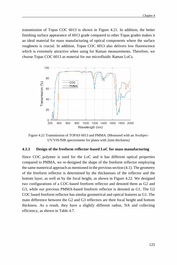
Chapter 4
125
transmission of Topas COC 6013 is shown in Figure 4.21. In addition, the better
finishing surface appearance of 6013 grade compared to other Topas grades makes it
an ideal material for mass manufacturing of optical components where the surface
roughness is crucial. In addition, Topas COC 6013 also delivers low fluorescence
which is extremely attractive when using for Raman measurements. Therefore, we
choose Topas COC 6013 as material for our microfluidic Raman LoCs.
Figure 4.21 Transmission of TOPAS 6013 and PMMA. (Measured with an AvaSpec-
UV/VIS/NIR spectrometer for plates with 2mm thickness)
4.3.3 Design of the freeform reflector-based LoC for mass manufacturing
Since COC polymer is used for the LoC and it has different optical properties
compared to PMMA, we re-designed the shape of the freeform reflector employing
the same numerical approach as mentioned in the previous section (4.1). The geometry
of the freeform reflector is determined by the thicknesses of the reflector and the
bottom layer, as well as by the focal height, as shown in Figure 4.22. We designed
two configurations of a COC-based freeform reflector and denoted them as G2 and
G3, while our previous PMMA-based freeform reflector is denoted as G1. The G2
COC based freeform reflector has similar geometrical and optical features as G1. The
main difference between the G2 and G3 reflectors are their focal height and bottom
thickness. As a result, they have a slightly different radius, NA and collecting
efficiency, as shown in Table 4.7.

Chapter 4 Integrated Confocal Raman Probe Combined with a Freeform Reflector Embedded Lab-on-Chip
126
Figure 4.22 Geometry of the freeform reflector.
Table 4.7 Specifications of the freeform reflectors.
G1:PMMA G2:COC G3:COC
Focal Height (µm) 50 50 100
Bottom Thickness (µm) 200 200 250
Reflector Thickness (µm) 300 300 300
NA 1.28 1.28 1.27
Radius (mm) 0.841 0.853 0.925
Efficiency 42% 42% 39%
The profiles of the PMMA-based freeform reflector and the two types of COC-based
freeform reflector are illustrated in Figure 4.23.
Figure 4.23 Profiles of the PMMA- and COC-based freeform reflectors.
The profile of the freeform reflector obtained by our numerical approach is a set of
data points, which needs to be fitted into a polynomial curve for the design and
fabrication of master molds, needed for double-sided hot embossing in a next step.
Therefore, we investigated the curve fitting of the surface profiles to find the proper
polynomial coefficients for the fabrication. The polynomial results of different

Chapter 4
127
degrees for both the PMMA- and COC-based freeform reflector are illustrated in
Figure 4.24, Figure 4.25 and Figure 4.26, and listed in Table 4.8.
Figure 4.24 Polyfitting results for the PMMA-based G1 chip.
Figure 4.25 Polyfitting results for the COC-based G2 chip.
Figure 4.26 Polyfitting results for the COC-based G3 chip.

Chapter 4 Integrated Confocal Raman Probe Combined with a Freeform Reflector Embedded Lab-on-Chip
128
Table 4.8 Polynomial fitting results of different freeform reflector designs.
(unit in mm) Poly2 Poly4 Poly6 Poly8 Poly10 Poly12 Poly14 Poly16
G1 Mean -1.76E-03 5.44E-04 -1.01E-04 -1.23E-05 1.59E-05 -3.53E-06 -1.50E-06 1.20E-06
STD 2.05E-03 5.58E-04 8.11E-05 2.94E-05 1.69E-05 3.11E-06 2.58E-06 1.16E-06
PV 5.93E-03 2.56E-03 2.27E-04 1.85E-04 5.35E-05 8.92E-06 1.42E-05 5.00E-06
G2 Mean -2.62E-03 7.47E-04 -6.74E-05 -5.34E-05 2.09E-05 4.12E-06 -4.85E-06 1.92E-07
STD 2.98E-03 7.01E-04 6.68E-05 6.57E-05 1.69E-05 8.91E-06 4.54E-06 1.41E-06
PV 7.89E-03 2.91E-03 3.09E-04 3.42E-04 4.89E-05 5.51E-05 1.27E-05 8.92E-06
G3 Mean -2.09E-03 4.24E-04 -3.84E-05 -1.30E-05 5.79E-06 -1.95E-07 -5.63E-07 1.63E-07
STD 2.20E-03 3.99E-04 2.77E-05 1.70E-05 5.19E-06 7.11E-07 6.37E-07 1.28E-07
PV 5.54E-03 1.79E-03 7.81E-05 1.01E-04 1.49E-05 4.80E-06 2.87E-06 3.73E-07
The accuracy of polynomial fitting of the reflector’s surface profile will greatly affect
the optical performance of the LoC system. The total integrated scatter (TIS) is
considered in the design to evaluate the influence of the surface quality of the reflector.
The TIS of an optical surface or thin film coating is given by33
𝑇𝐼𝑆(𝑅𝑞) = 𝑅0[1 − 𝑒−(4𝜋𝑅𝑞 cos 𝜃𝑖
𝜆)2
] (4.5)
Where, 𝑅𝑞 is the RMS roughness of the surface, 𝜃𝑖 is the angle of incidence, 𝑅0 is the
total reflectance, 𝜆 is the wavelength of the incident light. Figure 4.27 shows the
changes of scattering proportions of an optical surface with respect to the incident
angle and surface roughness for 785nm excitation light.
Figure 4.27 TIS of a reflective surface for 785nm wavelength light with different incident
angles.

Chapter 4
129
As stated by the TIS equation, incident light with a shorter wavelength gives rise to a
larger TIS for a surface with the same RMS roughness. In general, in order to
guarantee that the TIS is less than 20% for the 785nm excitation in our design, the
RMS roughness Rq should be less than 30nm. The requirement to the surface
roughness should be fulfilled during both the design and the fabrication phase.
According to the accuracy of the polynomial fitting listed in Table 4.8, a fitting degree
of 14 or higher is necessary.
Besides, we also determined the tolerance of the bottom thickness of the COC-based
chips via non-sequential ray tracing simulations in ASAP. The layout of our
simulation model is the same as the one used for the PMMA-based chip. We just
replace the PMMA-based chip with the COC-based 50µm/100µm focus LoC. The
normalized simulation results are shown in Figure 4.28. The maximum collection
efficiency of the G2 (50µm focal height) design is slightly higher than the one of the
G3 (100µm focal height) design because of its higher NA. However, we can observe
that the G3 design has a higher tolerance of the bottom thickness compared to the G2
design. This is mainly because the collection efficiency decreases sharply at a bottom
thickness of 50µm. This can be explained by the fact that most of the excitation rays
focus in the polymer bottom layer rather than in the microfluidic channel, resulting in
a higher Raman response of the COC polymer that obscures the Raman response of
the sample. For each design, in order to ensure that the normalized flux is more than
80%, the thickness error needs to be less than 20µm. This thickness tolerance is
particularly important in the follow-up fabrication process.
Figure 4.28 Thickness tolerance of the bottom thickness. The nominal bottom thickness of the
50µm focus design (G2) is 200µm, while the nominal bottom thickness of the 100µm focus
design (G3) is 250µm.

Chapter 4 Integrated Confocal Raman Probe Combined with a Freeform Reflector Embedded Lab-on-Chip
130
Base upon the simulations, we decided to investigate both designs and work in a first
step with the G2 chip.
4.3.4 Double-sided hot embossing for the 50µm focus G2 LoC
Design of the COC-based G2 chip
In a first step, we fabricated the COC-based 50µm focus G2 chip by double-sided hot
embossing replication. We have introduced the hot embossing fabrication process for
a microfluidic LoC in Chapter 1. Double-sided hot embossing is the replication
technique that stamps 3D structures on both sides of a polymer sheet by raising the
temperature of the polymer slightly above its glass transition temperature using two
master molds from both sides. Double-sided hot embossing is an ideal fabrication
technique for low-volume mass-manufacturing of optofluidic LoC devices where high
precision and high surface quality are essential34. Unlike the PMMA-based LoC for
which the reflector and the channel layer are fabricated out of different polymer plates,
the reflector, microfluidic channel and chamber can be stamped out of a single COC
plate. Next, we can bond the sealing layer on top of the hot-embossed replica by UV
curing adhesive. Thanks to the high overlay accuracy (2 µm) of the hot embossing
machine, we find that the alignment precision between the freeform reflector and
fluidic chamber of the COC-based G2 chip is higher than the precision of the PMMA-
based chip where the alignment had to be adjusted manually. This has also greatly
reduced the complexity and cost of the chip fabrication. Figure 4.29 and Figure 4.30
illustrate the structure and dimensions of our COC-based G2 chip. The diameter of
the channel/reflector layer is 25.4mm, the size of the sealing layer is 25.4 × 25.4 mm².
Figure 4.29 Drawing of the COC-based 50µm focus G2 chip with integrated freeform
reflector. The channel/reflector layer of the chip is fabricated via double-sided hot embossing.

Chapter 4
131
Figure 4.30 Dimensions of the COC-based 50µm G2 chip.
Fabrication of the brass-based master molds
Before we can replicate the COC-based G2 LoC by double-sided hot embossing, we
fabricated the master molds from brass material with ultra-precision diamond tooling.
Figure 4.31 shows the fabrication procedure of the reflector mold. A brass plate is first
prefabricated with a CNC milling machine and polished by diamond turning. Then
the mold structure for the reflector and rim of the chip are fabricated by ultra-precision
diamond tooling with the Nanotech 350FG CNC machine. The channel mold is
fabricated by micro-milling with the same Nanotech 350FG CNC, as shown in Figure
4.32.
Figure 4.31 Photographs of ultra-precision diamond tooling for the reflector mold fabrication.
(left: before tooling; middle: during tooling; right: after tooling)

Chapter 4 Integrated Confocal Raman Probe Combined with a Freeform Reflector Embedded Lab-on-Chip
132
Figure 4.32 Photograph of micro-milling for the channel mold fabrication.
The drawings and photos of the reflector and channel molds are illustrated in Figure
4.33. As the surface roughness of the replicas is highly dependent on the surface
quality of the molds, we characterized the surface of the reflector and channel molds
by using a non-contact optical profiler (Bruker Contour GT-I) based on a Mirau
interference microscope. We measured an RMS roughness of (20.5 ± 5.3) nm for the
reflector mold, and an RMS roughness of (6.4 ± 1.3) nm for the channel mold. Each
mold is evaluated within 10 evaluation areas of 64µm × 48µm.
Figure 4.33 Drawings and photographs of the reflector mold (left) and channel mold (right).

Chapter 4
133
Chip replication
To fabricate the COC-based 50µm focus G2 chips, the reflector and channel mold are
first fixed on the holders of the machine. Then, a Topas COC 6013 polymer sheet with
a dimension of 30mm × 30mm × 1mm is inserted into the chamber of the embossing
machine between the two molds. By increasing the temperature of the molds to 175°C
for 30 seconds and loading 12000N force under vacuum conditions, the micro-
structures of the fluidic channel as well as the freeform reflector are stamped on the
polymer sheet due to thermal plastic deformation. For demolding, the polymer is
cooled down to 115°C, while maintaining the applied force to avoid sink marks, voids
and shrinkage. These optimized parameters such as temperature, force and waiting
time guarantee that the bottom thickness of the replica is within the tolerance range,
which is crucial for our Raman signal acquisition. Finally, the stamped part is
demolded and removed from the machine. The cycle time for each replica takes
approximately 5 minutes. Figure 4.34 shows a schematic and photo of the double-
sided hot embossing process.
Figure 4.34 (a) Schematic and (b) photograph of double-sided hot embossing for the chip
replication.
Of course, other combinations of these factors are also able to control the bottom
thickness within the tolerance range. For instance, increasing the force while reducing
the waiting time and keeping the temperature constant, or keeping the force
unchanged, but lowering the temperature and extending the waiting time. Adjusting
all three factors is also possible to achieve the same objective. But when doing that,
we must take into account the corresponding possible consequences. For example,
increasing the force may not only deform the polymer sheet, but also the metal molds.
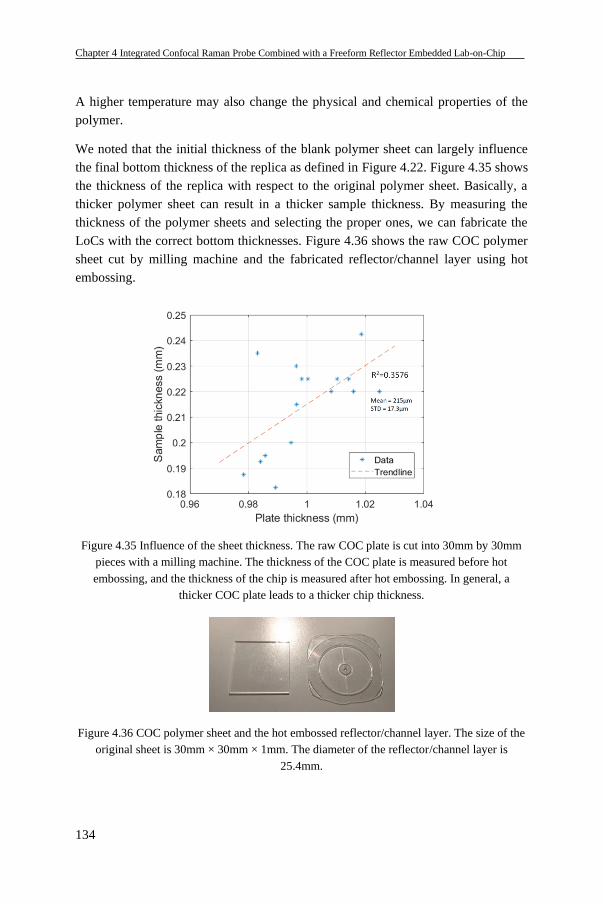
Chapter 4 Integrated Confocal Raman Probe Combined with a Freeform Reflector Embedded Lab-on-Chip
134
A higher temperature may also change the physical and chemical properties of the
polymer.
We noted that the initial thickness of the blank polymer sheet can largely influence
the final bottom thickness of the replica as defined in Figure 4.22. Figure 4.35 shows
the thickness of the replica with respect to the original polymer sheet. Basically, a
thicker polymer sheet can result in a thicker sample thickness. By measuring the
thickness of the polymer sheets and selecting the proper ones, we can fabricate the
LoCs with the correct bottom thicknesses. Figure 4.36 shows the raw COC polymer
sheet cut by milling machine and the fabricated reflector/channel layer using hot
embossing.
Figure 4.35 Influence of the sheet thickness. The raw COC plate is cut into 30mm by 30mm
pieces with a milling machine. The thickness of the COC plate is measured before hot
embossing, and the thickness of the chip is measured after hot embossing. In general, a
thicker COC plate leads to a thicker chip thickness.
Figure 4.36 COC polymer sheet and the hot embossed reflector/channel layer. The size of the
original sheet is 30mm × 30mm × 1mm. The diameter of the reflector/channel layer is
25.4mm.

Chapter 4
135
The surface roughness of the freeform reflector and the channel for the first set of
replicas (20 pieces) is (29 ± 4.9) nm and (24.8 ± 3.0) nm respectively, measured by a
non-contact optical profiler (Bruker Contour GT-I). We then applied a 200nm thick
reflective Au layer on the freeform reflector by sputter coating. In a last step, the
reflector/channel layer is bonded with a sealing layer by UV curing adhesive (Loctite
AA 3301 LC, Viscosity 160 mPa·s), as shown in Figure 4.37.
Figure 4.37 Photographs of the microfluidic lab-on-chip with integrated freeform reflector.
The hot embossed circular reflector/channel layer and the squared sealing layer are bonded by
UV curing adhesive.
Mold degradation and micro-cracks in the replicas
When repeating the hot embossing process to fabricate a second batch of COC-based
50µm focus G2 LoCs, we found that the surface quality of both molds and the replicas
degraded a lot. The RMS roughness of the reflector and the channel mold became
(168.1 ± 23.8) nm and (67.9 ± 16.2) nm respectively, as shown in Figure 4.38. The
RMS roughness of the corresponding replicas are (162.3 ± 21.9) nm and (69.2 ± 13.5)
nm respectively.
Figure 4.38 Surface roughness of the reflector and the channel mold before and after hot
embossing. The RMS roughness of the reflector mold increased from (20.5 ± 5.3) nm to
(168.1 ± 23.8) nm, and the RMS roughness of the channel mold increased from (6.4 ± 1.3) nm
to (67.9 ± 16.2) nm, respectively.

Chapter 4 Integrated Confocal Raman Probe Combined with a Freeform Reflector Embedded Lab-on-Chip
136
The deterioration of the mold’s surface roughness is mainly caused by two reasons.
Firstly, the high temperature during the hot embossing process can easily induce
oxidation and corrosion of the copper on the surface of the mold. Although the
replication is performed under vacuum conditions, the humidity, oxygen and other
gases adsorbed by the COC polymer can be released and adsorbed by the brass surface
during the hot embossing process. According to the datasheet of Topas, COC polymer
absorbs 100ppm humidity, 600ppm oxygen and 1200ppm nitrogen in general
conditions at 25°C. Because of the humidity, the copper surface easily adsorbs or
agglomerates H2O molecules resulting in a thin aqueous film. In this way, the
corrosion or electrochemical corrosion is more likely to occur. The released residuals
of the COC polymer are dissolved in the aqueous film and will greatly accelerate the
oxidation and corrosion of the copper at high temperatures. The higher the
temperature, the faster the reaction. The oxidation and corrosion can also be visually
observed through the discoloration of the brass surface. Secondly, the high pressure
applied on the microstructures during the hot embossing leads to a deformation of the
brass surface, which results in a degradation of the surface quality at macro scale. In
addition, heat can be hardly dissipated from the closed structure between two molds,
locally resulting in a higher temperature, which further aggravates the oxidation and
corrosion of the brass surface.
The degradation of the surface roughness of the molds naturally leads to a decreased
surface quality of the COC replicas. In addition, we even observed some micro-cracks
at the thinnest part (200µm bottom thickness) of the replicas around the reflector.
Some of the micro-cracks spread into the interior region of the freeform reflector,
which inevitably reduce the optical and mechanical properties of the LoCs, and
eventually affect the Raman detection efficiencies. The cracking defects are caused
by the shrinkage of the material during cooling35 because the mechanical strength of
the thinnest parts is much less than the surrounding regions. The cracking defects of
the COC replicas can be reduced by increasing the bottom thickness. Therefore, we
switched to the G3 LoC design by optimizing the structure of our LoC and the
fabrication process to solve problems such as the variation of the bottom thicknesses
and the degradation of the surface quality.
4.3.5 Mass fabrication of the COC-based 100µm focus G3 LoC
Design of the COC-based G3 LoC
The 100µm focus G3 LoC design has a bottom thickness of 250µm, which reinforces
the mechanical strength of the bottom layer and avoids cracking defects compared to
the G2 LoC design (200µm bottom thickness). We introduced fluorinated ethylene
propylene (FEP) tubing (IDEX Health & Science) instead of fused silica capillaries

Chapter 4
137
because of their higher flexibility and extreme resistance to a chemical attack36. A
general view of our COC-based G3 LoC is shown in Figure 4.39(a). Figure 4.39(b)
indicates the dimensions of our G3 LoC. The diameter of the freeform reflector is
1.851mm, the bottom thickness is 250µm. The integrated reflector/channel layer is
bonded with a circular sealing layer. The FEP tubing is inserted into the two holes of
the sealing layer that work as in- and outlet. The smallest volume we can measure
with the G3 LoC is 0.5µL which corresponds to the dimensions of the microfluidic
chamber.
Figure 4.39 (a) General view and (b) cross-section of the COC-based G3 LoC.
Fabrication process
The optimized fabrication process is shown in Figure 4.40. In a first step, we
fabricated two baseplates by CNC milling starting from brass material. A nickel
phosphorus (NiP) alloy layer was coated on top of each baseplate by electrochemical
plating. This NiP coating can improve the resistance of the brass mold to chemical
erosion and oxidation, especially when embossing at high temperatures.37 Next the
rough NiP surfaces on the brass molds were pre-milled before placing on the Nanotech
350FG CNC machine to obtain a good surface quality. In a next step, the reflector
mold was fabricated by ultra-precision diamond tooling and the channel mold by
micro-milling. Figure 4.41 shows the fabricated master molds out of NiP-coated brass.

Chapter 4 Integrated Confocal Raman Probe Combined with a Freeform Reflector Embedded Lab-on-Chip
138
Figure 4.40 Full fabrication flow for the COC-based 100µm focus G3 LoCs.
Figure 4.41 Photographs of the (a) reflector mold and (b) channel mold. The mold surface is
coated with NiP material.
The NiP-coated brass molds are then fixed on the hot embossing machine. Unlike the
fabrication of the COC-based G2 chip where the thickness of the replica was
controlled by the hot embossing settings and the dimensions of the polymer plate, we
designed and fabricated a physical stopper to control the bottom thickness of the
replicas, as shown in Figure 4.42. The physical stopper is equipped with 4 metal shims
and fixed around the reflector mold. When conducting the hot embossing process, we
put a 1mm-thick COC sheet in-between the two molds. By increasing the temperature
in the vacuum chamber and loading force on the molds, the polymer is deformed and
its thickness is decreased. The movement of the two molds will be stopped once both
molds hit the metal shim. In this way the 250µm thickness of the bottom layer can be

Chapter 4
139
precisely controlled, no matter how much the thickness of the raw polymer sheet
varies.
Figure 4.42 (a) General view and (b) dimensions of the physical stopper to control the bottom
thickness of the LoC during hot embossing. The thickness of each shim is 250µm.
In a next step, we applied a 200nm Au layer on the freeform reflector surface using a
sputter coater (JEOL® JFC-2300HR FINE COATER). The surfaces of the
reflector/channel layer as well as the sealing layer were treated with a Piezobrush®
PZ2 plasma pen to increase the surface energy and activate the polymers due to outer
chain scissions in just a few seconds.38–40 As a result, the adhesion of the polymer
surface can be improved during bonding using a thermal treatment or UV curing.
Figure 4.43 shows our final COC-based G3 chip.
Figure 4.43 Photographs of the fabricated COC-based 100µm focus G3 chip.
The RMS surface roughness of our optimized NiP-coated brass reflector and channel
mold are (12.4 ± 2.3) nm and (6.3 ± 0.4) nm respectively. The surface roughness of
the reflector and channel of the hot embossed G3 replica chip are (17.0 ± 3.9) nm and
(8.1 ± 0.4) nm respectively. After several runs, we did no longer observe a degradation
of the NiP-coated brass mold, and only regular cleaning of the molds’ surfaces with
isopropyl alcohol or acetone is needed to remove the residues, paving the way towards
the mass fabrication of our COC-based G3 chips.

Chapter 4 Integrated Confocal Raman Probe Combined with a Freeform Reflector Embedded Lab-on-Chip
140
4.3.6 Bonding and shear strength tests
We performed shear strength tests on the COC 6013 and PMMA samples bonded with
different approaches including UV curing adhesive, laser welding and thermal
bonding to better understand the improvement of plasma treatment on the adhesion of
polymers. Each sample under test consists of two COC or PMMA sheets with a
dimension of 25mm × 25mm × 1mm and an overlapping area of 10mm × 25mm, as
illustrated in Figure 4.44. The contact surface of each polymer sheet is exposed to a
plasma for 30 seconds with a Piezobrush® PZ2 plasma pen. For the UV curing
adhesive, a droplet of 50µL UV glue (Loctite AA 3301 LC) is placed on the
overlapping area and evenly distributed due to capillary forces. After illuminating the
glue with a UV lamp for 30 seconds, the two polymer sheets are bonded. The laser
welding is performed on a LPKF PrecisionWeld 3000 machine that is equipped with
a 1940nm-wavelength Thulium fiber laser with a spot size of 65µm. The power
density for the laser welding is 2.11kW/mm2. The laser spot on the interface of the
sheets melts the thermoplastic and generates physio-chemical bonds at the interface
by subsequent cooling41. The weld pattern is formed with 3 vertical lines (20mm long
each) and 6 horizontal lines (8mm long each), as shown in Figure 4.44(b). The total
weld seam area is 21.24mm2 approximately. The thermal bonding is performed using
the Jenoptik HEX04 hot embossing machine, which we also applied for the mass
fabrication of the chips. During the thermal bonding, we heated the sample up to
140°C and continuously applied a force of 1000N for 5 minutes. Here, a lower
temperature and force, compared to the replication of the chips, are applied to avoid
deformation of the polymer sheets.
Figure 4.44 (a) Scheme of UV/thermal bonding and (b) laser welding.
The bonded samples are placed into a Universal Testing Machine with both ends being
fixed in separate clamps. The shear stress 𝐹𝑝, coplanar with the overlapping plane, is
measured as shown in Figure 4.45. The samples without surface plasma treatment are
also tested as benchmark. The shear stress of the bonded samples with surface plasma
treatment is significantly improved except for thermal bonding. Because the plasma
treatment breaks some of the chemical bonds of the polymers on the surface, we

Chapter 4
141
understand it is easier to reconnect with the bonds of molecules from another polymer
sheet in the weld seam area or from the UV photoresist. While for the thermal bonding,
the heat and loaded force make the two polymer components to join permanently into
a complete assembly by cohesive bonds across the interface,41 the improvement in
adhesion by plasma treatment is not obvious.
Figure 4.45 Shear stresses of the samples bonded with different methods. (LW: laser welding;
UV: UV curing adhesive; TB: Thermal bonding; legend: with and without plasma treatment)
The shear strength of the bonding is given by42
𝜏 =𝐹𝑝
𝐴 (4.6)
Here A is bonding area, and 𝐹𝑝 is the shear stress measured. The calculated shear
strength of plasma treated, and non-plasma treated samples are listed in Table 4.9.
Table 4.9 Shear strength of different bonding approaches for different materials. (unit: MPa)
Method - Material Shear strength without PT Shear strength with PT
LW - COC 8.12 ± 4.71 32.02 ± 3.07
LW - PMMA 21.11 ± 2.21 26.47 ± 10.03
UV - COC 0.80 ± 0.27 1.08 ± 0.27
UV - PMMA 1.14 ± 0.30 3.55 ± 0.52
TB - COC 3.40 ± 0.89 3.45 ± 0.33
(PT: Plasma treatment. LW: laser welding; UV: UV curing adhesive; TB: Thermal bonding)
The laser welded COC sample with prior plasma treatment possesses the highest shear
strength 𝜏 compared to UV curing and thermal bonding. However, the weld seams
may deform the microfluidic channel and could lead to leakage. UV curing adhesive,
on the other hand, is a fast and simple bonding method, but only suitable for low-
speed and low-volume prototyping of LoC devices. Thermal bonding has the highest

Chapter 4 Integrated Confocal Raman Probe Combined with a Freeform Reflector Embedded Lab-on-Chip
142
resistance to the leakage for the COC material which is important for high-pressure
microfluidic detection.43
4.4 Mass manufactured LoCs in combination with the developed
Raman probe
4.4.1 Implementation of the proof-of-concept demonstration for confocal
measurements
We used the proof-of-concept setup of the Raman probe shown in Figure 4.15 in
combination with our hot embossed LoCs for the confocal microfluidic Raman
measurements, as shown in Figure 4.46.
Figure 4.46 Proof-of-concept Raman setup by combining the Raman probe with the mass
fabricated LoC. (BPF: Band-pass filter, M: Mirror, DM: Dichroic mirror, LPF: Long-pass
filter, NF: Notch filter, CL: Collimating lens, MMF: Multi-mode fiber.)
4.4.2 System calibration
In a first step, we perform Raman measurements with our confocal Raman setup to
calibrate the system. The Raman setup is aligned by adjusting the positions of the
optical components and the LoC to the optimal conditions. We compare the
performance of the hot embossed G2 and G3 chips by measuring the spectra of ethanol,

Chapter 4
143
as shown in Figure 4.47. The power of the laser excitation is 190mW, and the
integration time of the spectrometer is 15 seconds for each spectrum. In general, the
average Raman signal obtained by our 100µm focus G3 chip is 3 times larger as the
one obtained by the G2 chip. In addition, the repeatability of the spectra by the G3
chip is also much better than for the G2 chip. This can be explained by the lower
energy loss according to the smaller surface roughness and higher precision of the
bottom thickness of the G3 chip compared to the G2 chip.
Figure 4.47 Raman spectra of ethanol obtained by the mass fabricated G2 and G3 chips. The
dashed lines refer to the upper and lower range of the spectra. Figures are on the same scale.
Since the G3 chip performs twice better than the G2 chip, we continue with our G3
chip and calibrate our Raman system by measuring the Raman spectra of urea
solutions with different concentrations ranging from 2.5mM to 500mM, as shown in
Figure 4.48. The Raman peak at 930cm-1 comes from the background of COC polymer.
An internal standard with a constant concentration of 100mM KNO3 is added to each
urea solution for each measurement to eliminate uncontrollable fluctuations induced
by the setup.

Chapter 4 Integrated Confocal Raman Probe Combined with a Freeform Reflector Embedded Lab-on-Chip
144
Figure 4.48 Raman spectra of urea solutions with different concentrations. An internal
standard of 100mM KNO3 is added to the solution to normalize the spectra.
After subtracting the background of the water spectra, we normalize the Raman peak
of urea at 997cm-1 to the characteristic peak of KNO3 at 1040cm-1 for each urea
solution. Figure 4.49 shows the calibration curve with the changes of the normalized
Raman intensities of urea for different concentrations. The limit of detection (LOD),
or the detection limit, of the system can be obtained according to the calibration
curve:44
𝐿𝑂𝐷 = 3𝑆𝑎/𝑏 (0.32)
Where 𝑆𝑎 is the standard deviation of the response, and b is the slope of the linear
regression fitted calibration curve.
The LOD of our Raman probe in combination with the freeform reflector embedded
LoC is 10.2mM (60 ppm) for the detection of urea according to the linear regression
approach. The noise-equivalent-concentration (NEC) of our setup is 3.4mM for urea
detection, which is almost 6 times better than the NEC obtained with the LoC system
available at the start of this PhD. The LOD of our polymer-based Raman LoC is
comparable with the one obtained by the quartz glass-based Raman-on-chip (7.5mM)
with a much higher excitation power (700mW) 5,6.

Chapter 4
145
Figure 4.49 Calibration curve of our proof-of-concept Raman setup using our mass-fabricated
G3 chips in combination with our Raman probe.
4.4.3 Proof-of-concept for mycotoxin detection
As we mentioned in the previous chapter, mycotoxins including fumonisin45–47 and
deoxynivalenol48,49 are commonly existing in a variety of different crops. Their
detection is of great importance in the field of food safety. Therefore, we prepared
fumonisin and deoxynivalenol solutions with different concentrations and performed
Raman measurements using our Raman setup. The fumonisin B1 is dissolved in a 1:1
water-acetonitrile solution and the concentration of fumonisin B1 is prepared in three
levels: 2 ppb, 1250 ppb and 1500ppb, which are marked with the initial letter of the
toxin name, namely F followed by the numbers 1, 2 and 3, respectively. The
deoxynivalenol is dissolved with methanol and various concentrations (5 ppb, 1000
ppb and 1250 ppb) are prepared, marked with the initial letter of the toxin name,
namely D followed by numbers 1, 2 and 3, respectively. Each mycotoxin solution is
injected into the microfluidic channel of our COC-based G3 chip through the inlet,
and 10 sets of Raman spectra with 15 seconds integration time are obtained under the
785nm wavelength laser with a power of 190mW. The Raman spectra of the solvents
are also measured under the same conditions as reference.
All spectra are imported in MATLAB and smoothed with a 2nd order Savitsky-Golay
filter. We corrected the offset of the spectra by taking into account the mean level of
the spectra within the smooth bands between 1670cm-1 and 2360cm-1. In a next step,
we performed Principal Component Analysis (PCA) to the processed Raman spectra
of fumonisin B1 and deoxynivalenol.

Chapter 4 Integrated Confocal Raman Probe Combined with a Freeform Reflector Embedded Lab-on-Chip
146
Figure 4.50 shows the PCA results of the fumonisin Raman spectra. The spectra form
well separated groups in the PC1-PC2 plane, which accounts for 96% of total variance.
According to Figure 4.50(c), the solvent (MWA) and F1 data are close to each other.
Although the samples are classified, they are not ordered along the PC1 direction
according to their contamination level. PC2 is equal for all groups except for F3,
therefore this difference could be related to the toxin itself.
Figure 4.50 PCA results of the fumonisin B1 Raman spectra. (a) Average spectra of solvent
and fumonisin b1 with different concentration levels. (b) loadings of different principal
components. (c) Scores of PC1 and PC2.
Figure 4.51 shows the PCA results of the deoxynivalenol Raman spectra. The spectra
form well separated groups in the PC1-PC2 plane, which account for 96% of total
variance, as shown in Figure 4.51(c). The group of pure methanol is not close to D1
as expected. The groups are also not ordered according to their contamination level
along either PC1 or PC2. Moreover, two methanol spectra mix up with the D3 group.

Chapter 4
147
Figure 4.51 PCA results of the deoxynivalenol Raman spectra. (a) Average spectra of solvent
and deoxynivalenol with different concentration levels. (b) loadings of different principal
components. (c) Scores of PC1 and PC2.
In conclusion, Raman spectra of mycotoxins obtained by our Raman setup show a
very good repeatability (tight group of replies), which allow to detect sensible
between-sample differences. However, these differences look more related to random
factors than to their contamination. Only in case of Fumonisin B1, a detection of
contamination seems possible (and only along the 2nd PC), but it should be confirmed
by analyzing some more heavily contaminated samples (above 100ppm). When low
contamination levels are analyzed with traditional Raman spectroscopy, even a very
small difference in sample preparation could have an effect comparable to or even
stronger than the toxin itself. Therefore, the combination of SERS with microfluidic
LoC is necessary to increase the sensitivity of our Raman spectroscopy measurements
for mycotoxin detection.
4.5 Conclusion
In the first part of this chapter, we introduced a confocal Raman spectroscopy system
designed and implemented by our research group, prior to the start of this PhD. The
Raman spectroscopy system consists out of a freeform reflector, an integrated lab-on-

Chapter 4 Integrated Confocal Raman Probe Combined with a Freeform Reflector Embedded Lab-on-Chip
148
chip and external optics, which can suppress the background signal from the out-of-
focus regions significantly. We achieved a noise-equivalent concentration of 20mM
for urea detection. The PMMA-based lab-on-chip with embedded freeform reflector,
manufactured directly by ultra-precision diamond tooling, is robust and performant
from a mechanical and optical point of view in terms of misalignment tolerance and
high NA respectively. However, the cost for the direct fabrication of the freeform
reflector is quite high as it is not compatible with mass manufacturing techniques. The
chemical resistance of PMMA material is also relatively low for various types of
analytes and solvents. In addition, the dimensions of the external optics of the Raman
system is still large such that we cannot use it for in-situ analyses.
Therefore, in a first step of this PhD, we integrated the components of the external
optics into a miniaturized Raman probe. We accessed the misalignment tolerances by
means of non-sequential ray tracing simulations as well as experiments. In a next step,
we re-designed the freeform reflector and the lab-on-chip from many aspects for the
purpose of mass fabrication. The new design of the LoC is based on Topas COC
material, which shows a higher chemical resistance and better optical properties
compared to PMMA. The shape of the freeform reflector is calculated via a numerical
approach according to Fermat’s principle. We fabricated NiP-coated brass master
molds, which are resistant to chemical erosion and oxidation during double-sided hot
embossing. The NiP coating on top of the brass structure also improves the strength
of the molds and results in a higher surface quality. We replicated COC-based LoCs,
bonded them with a sealing layer and inserted FEP tubing as in- and outlet.
We integrated the mass manufactured LoC with the miniaturized Raman probe and
implemented a proof-of-concept demonstration setup. We conducted various types of
experiments to get insight into the performance of our Raman setup. We calibrated
our Raman system by measuring the Raman spectra of urea solutions with different
concentrations. A noise equivalent concentration of 3.4mM and a limit of detection of
10.2mM for urea solution is achieved by our LoC system. Finally, we employed our
Raman system for the detection of two types of mycotoxin, fumonisin B1 and
deoxynivalenol, and performed Principle Component Analysis to the Raman spectra
obtained. The PCA results show that the Raman spectra of mycotoxins obtained by
our setup are clustered and allow to detect differences between various samples.
However, the sensitivity of our LoC system using traditional Raman measurements is
too low. Therefore, the combination of microfluidic-lab-on-chips with SERS is
necessary to extend the applicability of Raman spectroscopy.

Chapter 4
149
References
1. Watson, D. A. et al. A Flow Cytometer for the Measurement of Raman
Spectra. Cytom. Part A 73, 119–128 (2008).
2. Ngernsutivorakul, T. et al. Design and Microfabrication of a miniature fiber
optic probe with integrated lenses and mirrors for Raman and fluorescence
measurements. Anal Bioanal Chem 409, 275–285 (2017).
3. Bates, K. E. & Lu, H. Biophysical Perspective Optics-Integrated Microfluidic
Platforms for Biomolecular Analyses. Biophys. J. 110, 1684–1697 (2016).
4. De Coster, D. et al. Free-form optics enhanced confocal Raman spectroscopy
for optofluidic lab-on-chips. IEEE J. Sel. Top. Quantum Electron. 21, 1–9
(2015).
5. Neugebauer, U. et al. Diagnostics of tumor cells by combination of Raman
spectroscopy and microfluidics. Clin. Biomed. Spectrosc. Imaging II 8087,
80870J (2011).
6. Dochow, S. et al. Raman-on-chip device and detection fibres with fibre Bragg
grating for analysis of solutions and particles. Lab Chip 13, 1109 (2013).
7. Yamamoto, H. et al. Diagnosis and Treatment of Small-Intestinal Diseases.
Clin. Gastroenterol. Hepatol. 3565, 1010–1016 (2004).
8. Goetz, M. & Wang, T. D. Imaging and Advanced Technology Molecular
Imaging in Gastrointestinal Endoscopy. Imaging Adv. Technol. 138, 828–833
(2010).
9. Kudo, S., Tamura, S., Nakajima, T. & Yamano, H. Diagnosis of colorectal
tumorous lesions by magnifying endoscopy. Gastrointest. Endosc. 44, 0–6
(1996).
10. COONEY, T. F., SKINNER, H. T. & S. M. ANGEL. Comparative Study of
Some Fiber-Optic Remote Raman Probe Designs . Part II : Tests of Single-
Fiber , Lensed , and Flat- and Bevel-Tip Multi-Fiber Probes. Appl. Spectrosc.
50, 849–860 (1996).
11. F.Cooney, T., SKINNER, H. T. & S.M.Angel. Comparative Study of Some
Fiber-Optic Remote Raman Probe Designs. Part I: Model for Liquids and
Transparent Solids. Appl. Spectrosc. 50, 836–848 (1996).

Chapter 4 Integrated Confocal Raman Probe Combined with a Freeform Reflector Embedded Lab-on-Chip
150
12. Shim, M. G., Song, L. W. K., Marcon, N. E. & Wilson, B. C. Rapid
Communication In vivo Near-infrared Raman Spectroscopy : Demonstration
of Feasibility During Clinical Gastrointestinal Endoscopy. Photochem.
Photobiol. 72, 146–150 (2000).
13. Saar, B. G., Johnston, R. S., Freudiger, C. W., Xie, X. S. & Seibel, E. J.
Coherent Raman scanning fiber endoscopy. Opt Lett. 36, 2396–2398 (2012).
14. M.S.Bergholt et al. In Vivo Diagnosis of Esophageal Cancer Using Image-
Guided Raman Endoscopy and Biomolecular Modeling. Technol. Cancer Res.
Treat. 10, 103–112 (2011).
15. Komachi, Y., Katagiri, T., Sato, H. & Tashiro, H. Improvement and analysis
of a micro Raman probe. Appl. Opt. 48, 6–13 (2009).
16. Motz, J. T. et al. Optical fiber probe for biomedical Raman spectroscopy. Appl.
Opt. 43, 542–554 (2004).
17. Short, M. A. et al. Development and preliminary results of an endoscopic
Raman probe for potential in vivo diagnosis of lung cancers. Opt. Lett. 33,
711–713 (2008).
18. Jermyn, M. & Desroches, J. A miniature confocal Raman probe for
endoscopic use. Phys. Med. Biol. 54, 7077–7087 (2009).
19. Mo, J., Zheng, W. & Huang, Z. Fiber-optic Raman probe couples ball lens for
depth-selected Raman measurements of epithelial tissue. Biomed. Opt.
Express 1, 4712–4721 (2010).
20. Prasad, P. N. Nanophotonics. (John Wiley & Sons, Inc., 2004).
21. Cordero, E., Latka, I., Matthäus, C., Schie, I. W. & Popp, J. In-vivo Raman
spectroscopy : from basics to applications. J. Biomed. Opt. 23, 071210 (2018).
22. Sarychev, A. K., Ivanov, A., Lagarkov, A. & Barbillon, G. Light
Concentration by Metal-Dielectric Micro-Resonators for SERS Sensing.
Materials (Basel). 12, 1–39 (2019).
23. M.L.Myrick & S.M.Angel. Elimination of Background in Fiber-Optic Raman
Measurements. Appl. Spectrosc. 44, 565–570 (1990).
24. Ma, J. & Li, Y.-S. Optical-Fiber Raman Probe with Low Background
Interference by Spatial Optimization. Appl. Spectrosc. 48, 1529–1531 (1994).

Chapter 4
151
25. Archibald, D. D., Lin, L. T. & Honigs, D. E. Raman Spectroscopy over
Optical Fibers with the Use of a Near-IR FT Spectrometer. Appl. Spectrosc.
42, 1558–1563 (1988).
26. Yamada, H., Nozawa, M., Kinoshita, M. & Ohashi, K. Vertical-coupling
optical interface for on-chip optical interconnection. Opt. Express 19, 698
(2011).
27. Materials, O. F. Fatigue crack propagation of PMMA in organic sovents. 9,
1896–1898 (1974).
28. Arnold, J. C. The effects of diffusion on environmental stress crack initiation
in PMMA. J. Mater. Sci. 33, 5193–5204 (1998).
29. Topas Advanced Polymers. TOPAS - Cyclic Olefin Copolymers. 4 (2015).
Available at:
http://www.topas.com/sites/default/files/files/TOPAS_Brochure_E_2014_06
(1).pdf.
30. TOPAS® COC Products. Polyplastics Global Website (2020). Available at:
https://www.polyplastics-global.com/en/product/topas.html.
31. O’Neil, C. E., Taylor, S., Ratnayake, K., Pullagurla, S. & Soper, S. A.
Chracterization of Activated Cyclic Olefin Copolymer: Effects of Ethylene /
Norbornene Content on the Physiochemical Properties. Analyst 141, 6521–
6532 (2017).
32. Wu, J. et al. Cereus sinensis Polysaccharide and Its Immunomodulatory
Properties in Human. Mar. Drugs 15, 140 (2017).
33. Schröder, S., Herffurth, T., Duparré, A. & Harvey, J. E. Impact of surface
roughness on scatter losses and the scattering distribution of surfaces and thin
film coatings. in SPIE - The International Society for Optical Engineering
8169 1–8 (2011). doi:10.1117/12.896989
34. Leech, P. Hot Embossing Of Microchannels in Cyclic Olefin Copolymers. in
Mater. Res. Soc. Symp. Proc. OO03-01 (2009). doi:10.1557/PROC-1191-
OO03-01
35. Shin, H. & Park, E. Analysis of Crack Phenomenon for Injection-Molded
Screw Using Moldflow Simulation. J. Appl. Polym. Sci. 113, 2702–2708
(2009).

Chapter 4 Integrated Confocal Raman Probe Combined with a Freeform Reflector Embedded Lab-on-Chip
152
36. Rath, S. K., Palai, A., Rao, S., Chandrasekhar, L. & Patri, M. Effect of
Solvents in Radiation-Induced Grafting of 4-Vinyl Pyridine onto Fluorinated
Ethylene Propylene Copolymer. J. Appl. Polym. Sci. 108, 4065–4071 (2008).
37. Barycka, I., Hołodnik, B. & Misiuk, A. NiP as a New Material for Thick Film
Technology. Electrocompon. Sci. Technol. 7, 221–226 (1981).
38. Kaplan, S. L. & Rose, P. W. Plasma surface treatment of plastics to enhance
adhesion. Int. J. Adhes. Adhes. 11, 109–113 (1991).
39. Hegemann, D., Brunner, H. & Oehr, C. Plasma treatment of polymers for
surface and adhesion improvement. Nucl. Instruments Methods Phys. Res.
Sect. B Beam Interact. with Mater. Atoms 208, 281–286 (2003).
40. Noeske, M., Degenhardt, J., Strudthoff, S. & Lommatzsch, U. Plasma jet
treatment of five polymers at atmospheric pressure: Surface modifications and
the relevance for adhesion. Int. J. Adhes. Adhes. 24, 171–177 (2004).
41. Roy, P. K., Malik, T. & Sinha, T. K. Thermal bonded Nonwoven - An
Overview. TechnicalTextile.Net 1–15 (2011). Available at:
https://www.technicaltextile.net/articles/thermal-bonded-nonwoven-an-
overview-5402.
42. Pelsmaeker, J. De et al. Clear to clear laser welding for joining thermoplastic
polymers: a comparative study based on physicochemical characterization. J.
Mater. Process. Technol. 255, 808–815 (2017).
43. Rosenbergerl, F., Jones, E., Lee, C. & Devoe, D. HIGH PRESSURE
THERMAL BONDING FOR SEALING. Micro Total Anal. Syst. 1, 404–405
(2002).
44. Shrivastava, A. & Gupta, V. B. Methods for the determination of limit of
detection and limit of quantitation of the analytical methods. Chronicles
young Sci. 2, 21–25 (2011).
45. Marasas, W. F. O. Discovery and Occurrence of the Fumonisins : A Historical
Perspective. Environ. Health Perspect. 109, 239–243 (2001).
46. Lee, K., Herrman, T. J., Nansen, C. & Yun, U. Application of Raman
spectroscopy for qualitative and quantitative detection of fumonisins in
ground maize samples. IJRS 1, 1–14 (2013).
47. Lee, K. & Herrman, T. J. Determination and Prediction of Fumonisin

Chapter 4
153
Contamination in Maize by Surface – Enhanced Raman Spectroscopy
( SERS ). Food Bioprocess Technol 9, 588–603 (2016).
48. Yuan, J. et al. A rapid Raman detection of deoxynivalenol in agricultural
products. Food Chem. 221, 797–802 (2017).
49. Pestka, J. J. & Smolinski, A. T. Deoxynivalenol : Toxicology and Potential
Effects on Humans. J. Toxicol. Environ. Health 8, 39–69 (2015).


Chapter 5
155
Chapter 5
5 A Tunable Freeform Segmented Reflector in a
Microfluidic System for Conventional Raman
and SERS Spectroscopy
As we described in Chapter 2, Raman spectroscopy is a powerful optical detection
technique and nowadays it is widely used in biological research, pharmaceutics,
chemical sciences and many other fields1–6. When a bundle of photons interacts with
a molecule, the majority of the photons will be elastically scattered by the molecule
as Rayleigh scattering, while a small portion (typically millionths) of the photons will
be absorbed and re-emitted almost simultaneously by the molecule with a frequency
shift due to the molecular vibrational modes. The inelastic scattering of the photons
with energy shift is referred as Raman scattering, which can be captured and detected
by a spectrometer as a Raman spectrum. The Raman spectra contain fingerprint
information of the molecules under test that can be used for material characterization.
Raman spectroscopy is suitable for label-free analysis of solids, liquids and gases
qualitatively or quantitatively. Especially in recent years, the combination of a
microfluidic chip with Raman spectroscopy has largely reduced the size and cost
compared to traditional bulky Raman equipment7–9. One way to miniaturize the
Raman system is to remove the lenses for collimation and focusing but introduce
optical fibers directly into the microfluidic chip for excitation and collection
components10–13. The optical fiber-based Raman-on-chip systems are very compact.
In such systems, the distance between the fiber facets and the fluid should be as small
This chapter is based on a published article:
Liu, Q.; Stenbæk Schmidt, M.; Thienpont, H.; Ottevaere, H. A Tunable Freeform-Segmented
Reflector in a Microfluidic System for Conventional and Surface-Enhanced Raman
Spectroscopy. Sensors 2020, 20, 1250.

Chapter 5 A Tunable Freeform Segmented Reflector in a Microfluidic System for Conventional Raman and SERS
156
as possible, otherwise the excitation and collection efficiencies of the microfluidic
chip will decrease significantly. One way to satisfy this requirement is to keep the
fiber ends in the fluidic channel and be in contact with the sample directly. However,
the analytes can contaminate the fiber facets easily during a measurement, therefore
decreasing the reliability and stability of the Raman analysis. To prevent this, a
compromise is to miniaturize some of the optical components into micro-optics and
to integrate them with the microfluidic chip14,15. These optofluidic chips typically have
higher sensitivity in comparison with the fiber-based microfluidic chips due to the
higher excitation and collection efficiencies. We have introduced freeform reflector-
based PMMA and COC lab-on-chips for Raman spectroscopy with a noise-
equivalent-concentration (NEC) for urea solution of 20mM and 3.4 mM respectively
in Chapter 4. The lab-on-chip has suppressed the background of polymer - out of
which the chip is fabricated - by a factor of 7. Nevertheless, the cost of an individual
chip is very expensive since the freeform reflector embedded on the chip is fabricated
via ultra-precision diamond tooling with considerably high manual and equipment
requirements. In addition, the detection limit of our previous lab-on-chip with
conventional Raman spectroscopy is not low enough to satisfy the requirements for
biological and toxicological applications where the concentrations of the analytes are
typically at ppm or even ppb level. Spectroscopy based on Surface-Enhanced Raman
Spectroscopy (SERS) has been applied increasingly to reach a higher detection
sensitivity by integrating nanoparticles, nanodimers or specific SERS-biotags in the
microfluidic systems for drug and cell detection16–19. With SERS, the Raman
scattering of adsorbates can be enhanced by localized surface plasmon resonances
(LSPR) on rough metal surfaces or nanostructures with noble metallic coating such as
Au or Ag. The SERS enhancement factors are typically 104–106 and can be as high as
1012 for single molecule detection20–22. In this chapter we investigate a freeform
reflector-based tunable Raman spectroscopy setup for microfluidic lab-on-chip
analysis. Although COC is the material needed to achieve a better chemical resistance,
however in a first step to demonstrate the proof-of-concept, we use PMMA to
fabricate our lab-on-chip. The versatile Raman setup we built for the experimental
proof-of-concept demonstration is compatible with our own PMMA-based lab-on-
chip for conventional Raman and surface-enhanced Raman detection, as well as lab-
on-chips that are commercially available.

Chapter 5
157
5.1 Design of the freeform segmented reflector
5.1.1 An overview of the segmented reflector
The lab-on-chip, reported in Chapter 4, consists of three layers, as shown in Figure
5.1(a). The 200µm thick bottom layer is embedded with a freeform reflector with
200nm gold coating to focus the excitation beam and collect the scattered Raman
signal. The middle layer is a 500µm height fluidic layer for the sample flow. The top
PMMA layer is the sealing layer for the fluidic channel including in- and outlets. The
focal point of the freeform reflector is located in the fluidic layer 50µm above the top
of the reflector layer. The fixed freeform reflector on chip enables robust confocal
Raman detection but has no flexibility to introduce SERS, since the SERS affective
area is typically close to the surface of the metallic surface in a range smaller than
100nm. Moreover, the SERS substrates are covered with a metallic coating and
therefore opaque. The incident beam and the Raman scattered light will be blocked in
the reflector-based system when introducing the SERS substrate without any
modification.
Figure 5.1 Illustration of (a) our freeform reflector embedded lab-on-chip (NA=1.28)
discussed in Chapter 4 and (b) the segmented reflector-based Raman system with SERS
microfluidic chip (NA=1.15). The red and blue rays refer to the incident light that interact
with different segments of the reflector. (S1: center segment; S2: middle concave segment;
S3: marginal segment.)
To this end, we bring forward a segmented mirror design that works together with a
microfluidic chip, by which the majority of the excitation light can be utilized and all
the scattered light within a certain field can bypass the SERS substrate and can be
collected. The microfluidic chip consists of three layers, including the polymer-based
bottom and top sealing layers and a channel layer for the fluidic samples, as shown in
Figure 5.1(b). The reflector is composed of three segments, the center segment, the
middle concave segment and the marginal segment at the outer rim of the reflector. In

Chapter 5 A Tunable Freeform Segmented Reflector in a Microfluidic System for Conventional Raman and SERS
158
the excitation path, the majority of excitation light will be directly reflected to the
microfluidic channel by the middle segment. The outer part of the beam will firstly be
reflected by the marginal segment and then focused by the center segment to the same
focal point as that of the concave segment. Only a small amount of the excitation
energy is blocked by the SERS substrate. And vice versa, in the collection path, the
center segment and the marginal segment provide the Raman signal collection with
two reflective surfaces and can work together to collimate the Raman scattering close
to the optical axis. At the same time the middle segment can collimate the rest of the
Raman scattered light towards the same direction.
5.1.2 The middle concave segment design
There are two methods to design the middle segment, either by conventional
sequential ray tracing to reduce the various aberrations and obtain an optimal surface,
or by a numerical approach to calculate the surface profile directly. We will not
discuss the ray-tracing-based optimization method in this PhD but focus on the
numerical approach.
Figure 5.2 Surface profile of the concave segment, the parallel rays are reflected through the
bottom layer of the microfluidic chip into the channel layer.
As shown in Figure 5.2, the refractive index of the sample under test in the channel
and the bottom polymer layer are 𝑛1 and 𝑛2, respectively. Additionally, the medium
between the bottom polymer layer and the reflector has a refractive index of 𝑛3.
The excitation ray AB that is perpendicular to the microfluidic chip is reflected by the
concave surface at point 𝐶, enters the bottom layer of the microfluidic chip at point D
and is refracted to the upper surface of the polymer layer at point E. The angle of
incidence, angle of refraction and angle of emergence at the bottom polymer layer are
Chapter 5
159
𝜃1, 𝜃2, 𝜃3 respectively. 𝐹 is the focal point for all the excitation rays. Points 𝑂 and 𝐺
are the intersections of the central ray with the bottom and upper surfaces of the
bottom polymer layer, respectively. 𝑀 is the lowest point of the reflector’s surface.
Suppose the focal height, or the distance between the upper surface of the polymer
layer and the focal point, is ℎ𝑓. The thickness of polymer layer is ℎ𝑝, the distance
between the lower surface of the polymer layer and the reflector is ℎ𝑚.
According to Snell's law
𝑛1 sin 𝜃1 = 𝑛2 sin 𝜃2 = 𝑛3 sin 𝜃3 (5.1)
As stated by Fermat’s principle23, the optical path length of all rays leaving the
polymer layer of plane 𝑥 and focusing to point 𝐹 is a constant, namely
𝑛3 ∙ (𝐵𝐶 + 𝐶𝐷) + 𝑛2 ∙ 𝐷𝐸 + 𝑛1 ∙ 𝐸𝐹
= 2𝑛3 ∙ ℎ𝑚 + 𝑛2 ∙ ℎ𝑝 + 𝑛1 ∙ ℎ𝑓 (5.2)
Let’s construct a Cartesian coordinates system with point 𝑂 as the origin and the
central ray 𝑂𝐹 as the z-axis. Then the point 𝐶 on the surface of the reflector can be
represented by the coordinates (𝑥, 𝑧) . We can also get the following geometric
relationships
−𝑥 = 𝐵𝐶 ∙ tan 𝜃3 + ℎ𝑝 ∙ tan 𝜃2 + ℎ𝑓 ∙ tan 𝜃1 (5.3)
−𝑧 = 𝐵𝐶 (5.4)
𝐶𝐷 = −𝑧/ cos 𝜃3 (5.5)
𝐷𝐸 = ℎ𝑝/ cos 𝜃2 (5.6)
𝐸𝐹 = ℎ𝑓/ cos 𝜃1 (5.7)
When inserting the equations (5.3) - (5.7) into the equation (5.2) we get
𝑧 = [𝑛2ℎ𝑝(1
𝑐𝑜𝑠 𝜃2
− 1) + 𝑛1ℎ𝑓(1
𝑐𝑜𝑠 𝜃1
− 1) − 2𝑛3 ∙ ℎ𝑚]
/[𝑛3 ∙ (1 +1
𝑐𝑜𝑠 𝜃3
)]
(5.8)

Chapter 5 A Tunable Freeform Segmented Reflector in a Microfluidic System for Conventional Raman and SERS
160
Also, the abscissa of the surface 𝑥 is given by
𝑥 = 𝑧 ∙ tan 𝜃3 − ℎ𝑝 ∙ tan 𝜃2 − ℎ𝑓 ∙ tan 𝜃1 (5.9)
Because 𝜃2 and 𝜃3 can be represented by 𝜃1 according to equation (5.1), and as
demonstrated by the equation (5.8) and (5.9), we notice that once the ℎ𝑓, ℎ𝑝 and ℎ𝑚
are confirmed, the surface profile of the concave segment is a function of the angle
𝜃1. If we fill the same medium as 𝑛1 in the space between the polymer layer and the
reflector (𝑛1 = 𝑛3), 𝜃1 = 𝜃3. The focal height ℎ𝑓 will change proportionally with
respect to the height of reflector ℎ𝑚 , making the system tunable in the vertical
direction with a stationary spot size. This is crucial as we can place the focal point in
the very middle of the channel to minimize the Raman background from the polymer
or keep it exactly on the nanostructures of a SERS substrate maximizing the SERS
enhancement. Since most of the sample solutions for biological and chemical research
are aqueous24–27, and many other organic solvents such as ethanol or acetone have a
similar refractive index as water, we use water as the medium between the reflector
and polymer layer (𝑛1 = 𝑛3 = 𝑛𝑤𝑎𝑡𝑒𝑟).
5.1.3 The center and marginal segment design
The center and marginal segments are also directly designed by a numerical approach.
Figure 5.3 illustrates the surface profile of all three segments. In this step we use the
same Cartesian coordinates system as mentioned before.
Figure 5.3 Design schematic of all segments: center, concave and marginal: (a) general view,
(b) zoom-in view of the rays in the microfluidic channel and (c) zoom-in view of the rays
interacting with the center segment.

Chapter 5
161
Assume 𝑆𝑖(𝑥𝑠𝑖 , 𝑧𝑠𝑖) is the virtual focal point of a reflected ray by the concave surface,
which refers to the intersection of the extension of a reflected ray and the optical axis.
Note that 𝑆𝑖 is different from the actual focal point 𝐹, which can be obtained by ray
tracing of the reflected rays according to the surface shape of the concave segment.
𝑃𝑖(𝑥𝑖 , 𝑧𝑖) is a random point of the center segment. 𝑆𝑖𝑃𝑖 is the relevant ray that passes
through the same focal point of the concave segment. The angle of inclination of the
center segment at point 𝑃𝑖 is 𝜃𝑖. The angle between ray 𝑆𝑖𝑃𝑖 and the optical axis is 𝛼𝑖,
and the angle between ray 𝑆𝑖𝑃𝑖 and the reflected ray by center segment is 𝛽. 𝛽 is a
constant for all rays. The angle of inclination of the marginal segment is γ. M is the
end point of the concave segment profile.
For the ray S𝑖𝑃𝑖, its slope is given by
tan 𝛼𝑖 = (𝑥𝑖 − 𝑥𝑆𝑖)/(𝑧𝑖 − 𝑧𝑆𝑖) (5.10)
For the surface of center segment at point 𝑃𝑖 , the angle of inclination 𝜃𝑖 is given by
𝜃𝑖 = (𝛽 − 𝛼𝑖)/2 (5.11)
If we describe the center segment by
𝑧 = 𝑓(𝑥) (5.12)
Then the slope of center segment is given by
tan 𝜃𝑖 = (𝑧𝑖+1 − 𝑧𝑖)/(𝑥𝑖+1 − 𝑥𝑖) (5.13)
The numerical calculation of the surface profile of the center segment starts from the
initial point 𝑃0 that the radius of the center segment |𝑥0| is determined by the lateral
dimension of the SERS substrate. The angle value of 𝛽 can firstly be derived from the
inclination of ray 𝑃0𝑀. Then tan 𝛼0, the slope of the ray S0𝑃0, is obtained by equation
(5.10). The derived angle value of 𝛼0 is introduced to equation (5.11) to get the value
of 𝜃0. In a next step, the coordinate of 𝑃1(𝑥1, 𝑧1) is calculated as the intersection point
of ray S1𝑃1 and the curve 𝑃0𝑃1. The overall profile of the center segment is calculated
by iteration of this process from the coordinates of 𝑃1 to 𝑃𝑖 .
The profile of the marginal segment is a straight line with an angle of inclination that
is given by
𝛾 = (𝜋 − 𝛽)/2 (5.14)
Normally, the thickness of the polymer layer for the microfluidic chip should be larger
than 200µm to guarantee mechanical strength. To reduce the fabrication complexity,

Chapter 5 A Tunable Freeform Segmented Reflector in a Microfluidic System for Conventional Raman and SERS
162
we introduce a 1mm thick commercial polymer plate in our design, which is identical
to many other commercial microfluidic chips. We accomplished the segmented
freeform design of two configurations with a diameter of the center segment of 5mm
and 10mm respectively, as shown in Figure 5.4. The numerical aperture of both
configurations is 1.15, making their collecting efficiencies close to that of a 100×
magnification objective lens. The overall diameter of the segmented reflector
increases from 30mm to 38mm when the diameter of the center segment increases
from 5mm to 10mm. The sag of the whole reflector also increases with a larger inner
diameter. As a result, the tunability of the system decreases from 4mm to 0.5mm.
Since the 5mm diameter of the center segment is wide enough to cover the SERS
substrate for our application, we utilize the 5mm center segment design in the
following non-sequential ray tracing simulation, fabrication and experiments.
Figure 5.4 Two configurations of reflector and microfluidic chip design, the diameter of the
center segment for the (a) and (b) configurations are 5mm and 10mm, respectively, and the
overall diameters are 30mm and 38mm. NA of both configurations is 1.15. Moreover, the NA
of the center segment is 0.34 and 0.45 respectively. The blue and red rays refer to the incident
light that interact with different segments.
5.2 Non-sequential simulation of the Raman spectroscopy with
segmented reflector
We performed a non-sequential ray tracing simulation for our system using the
Henyey-Greenstein model in OpticStudio (Zemax, Kirkland, WA, USA). This model
was initialized by Henyey and Greenstein in 1941 to describe the angular distribution
of light scattered by interstellar matter28. Nowadays it has been applied as one of the
typical Rayleigh models in various situations, ranging from the scattering of light by
chemical emulsions29, biological tissues30 to atmospheric and interstellar clouds31.
Since Raman scattering has common features as Rayleigh scattering, the intensity of

Chapter 5
163
scattered light is inversely proportional to the fourth power of the wavelength of the
incident light and the size of particles (typically on the order of 1 nm) inducing the
scattering is much smaller than the wavelength of the excitation, we use this model
for our non-sequential simulations.
In the Henyey-Greenstein model28, the scattered light has the following angular
distribution 𝜌(𝜃)
𝜌(𝜃) = 1
4𝜋
1 − 𝑔2
(1 + 𝑔2 − 2𝑔 cos 𝜃)32
(5.15)
Where, 𝜃 is the angle of scattered light with respect to the incident light. 𝑔 is an
asymmetric factor ranging from -1 to 1. According to equation (5.15), the forward
scattering is dominant when g>0. While g<0, backscattering predominates. For an
oriented molecule or crystal, the angular distribution of Raman scattering is
heterogeneous32. But in most cases, as the molecules in the sample are randomly
oriented, so the Raman scattering is nearly isotropic in 4π steradian, we set g=0 to
simplify the simulation.
The other two important parameters of the Henyey-Greenstein model in Zemax
OpticStudio are transmission and mean free path33. The transmission parameter
indicates how much of the incident light is attenuated during scattering. The mean
free path (M) refers to the probability of the ray being scattered. In Zemax
OpticStudio, the integrated probability of a ray traveling a distance 𝑥 within the
medium and undergoing scattering is given by 33
𝑝(𝑥) = 1.0 − 𝑒−𝑥𝑀 (5.16)
The larger the value of M, the lower the probability that the incident light will be
scattered.

Chapter 5 A Tunable Freeform Segmented Reflector in a Microfluidic System for Conventional Raman and SERS
164
Figure 5.5 Non-sequential simulation in ZEMAX OpticStudio: (a) Overall layout, and (b) the
microfluidic chip and segmented reflector. The blue rays and green rays refer to the excitation
light and Raman light respectively. (EL: Excitation lens; CL: Collection lens; BP: Band-pass
filter; M: Mirror; LP: Long-pass filter; DM: Dichroic mirror.)
In addition to the microfluidic chip and segmented reflector, the microfluidic system
also contains external optics consisting out of an excitation path and a collection path
(Figure 5.5). In the excitation path, the excitation laser coming out of the facet of the
excitation fiber is collimated into a parallel beam by the excitation lens. A band-pass
filter (BP) is used to suppress the laser intensity at other frequencies. The mirror (M)
and dichroic mirror (DM) then reflect the collimated beam to a beam expander
consisting out of a concave and a convex lens. The expanded laser beam with the same
diameter of the segmented reflector passes through the microfluidic chip and focuses
inside the fluidic channel by the segmented reflector.
In the collection path, the generated Raman scattering is collimated by the reflector
and bypasses the central region of the microfluidic chip. Then the Raman beam is
reduced in diameter by the beam expander, passes through the dichroic mirror and the
long-pass filter, and is collected into the collection multi-mode fiber by the collection
lens.

Chapter 5
165
In the non-sequential simulation, the wavelength of excitation is 785nm, and the
wavelength of scattering is 850nm, which is close to the fingerprint Raman bands of
ethanol, urea and potassium nitrate. These chemicals are also the analytes we use in
the following experiments. For the microfluidic chip, the channel layer with fluidics,
as well as the two polymer layers can be defined as scattering volumes respectively in
accordance with the Henyey-Greenstein model. The thickness of each layer is 1mm.
We perform non-sequential ray tracing simulations to evaluate three characteristics of
our Raman system: confocality, background suppression, and alignment tolerances of
the external optics with respect to the reflector.
Our Raman system is a confocal system, in which the collection fiber works as the
pinhole to attenuate the out-of-focus scattering. In this confocal system, only the
scattering close to the focus will be collected into the multi-mode fiber (MMF).
Scattering from above or below the focal point is regarded as background and will be
suppressed due to the proper choice of the core diameter of the multi-mode fiber.
Figure 5.6 Confocal behavior of the system by simulation. Each subfigure shows the
efficiency changes with respect to the displacement of the point source in (a) x-, (b) y- and (c)
z-axis, respectively. 100µm, 200µm and 400µm MMF are used as collection fiber.

Chapter 5 A Tunable Freeform Segmented Reflector in a Microfluidic System for Conventional Raman and SERS
166
To evaluate the confocality, we place a point source in the fluidic channel to
demonstrate the Raman source from a molecule. The light from this point source can
be received by the MMF through the collection path. By displacing the point source
out of the optimal position in different directions and to detect the flux received on
the fiber tip, we can get the confocality curve, as shown in Figure 5.6. MMFs with
diameters of 100µm, 200µm and 400µm are modeled in our simulation. The collection
efficiency is defined as the proportion of Raman scattered light that can be collected
by our system over the entire 4π steradian of all Raman scattered light. If all backward
Raman scattering can be collected, the normalized efficiency should be 50%.
According to the simulation, a maximum normalized efficiency of 23.8% can be
realized by our Raman setup when using a 400µm MMF. After fitting the confocality
curve with a normal distribution, we can obtain the Full Width Half Maxim (FWHM)
of the flux change with respect to the displacement of the point source, as listed in
Table 5.1.
From the simulation result, we notice that a large core diameter of multi-mode fiber
leads to a higher collection efficiency, but a lower confocality with larger FWHM. It
is reasonable that more scattering from both the in-focus and out-of-focus regions are
collected with a larger core size. Besides, two extrema appear on the confocality curve
at the z direction. This is because the parameters of all the optical components for
simulation as well as experiments are from commercial companies, and the
aberrations when they are aligned together are relatively large, resulting in non-
parallel rays towards the reflector, thereby giving rise to separated focal points for
different segments of the reflector. This phenomenon is more obvious when the
diameter of MMF is small. Therefore, we should select a suitable fiber to get a trade-
off between efficiency and confocality for different scenarios.
Table 5.1 Confocality behavior of the setup from simulations.
MMF (µm) Max Efficiency Confocality - FWHM (µm)
x y z
100 13.4 % 41.8 35.2 120.0
200 19.3 % 57.8 57.4 124.6
400 23.8 % 100.0 100.4 155.6
Confocality refers to the system’s ability to suppress the background outside the
region of interest. However, it is very difficult to measure this parameter
experimentally because no perfect point source is available in reality. Therefore, we
use another related parameter, the suppression factor (SF), to represent the confocality
that is both theoretically and experimentally obtainable.

Chapter 5
167
In the simulation of confocal performance, we define the top, bottom and the channel
layer as scattering volume by the Henyey-Greenstein model. The Raman intensity
observed at the collection fiber from these layers are 𝐼𝑡 , 𝐼𝑏 and 𝐼𝑚 respectively with
the identical excitation. The suppression factor (SF) can be calculated via the
following equation in the simulation
𝑆𝐹 = 𝐼𝑚/(𝐼𝑡 + 𝐼𝑏) (5.17)
As our setup includes the segmented reflector, the microfluidic chip as well as the
external optics, the alignment of the different parts can be critical. Especially when
the collection fiber in the Raman probe plays the role of the pinhole in the confocal
system, a small displacement of the MMF can reduce the Raman intensity obtained.
To assess the influences of the misalignment, we displace the MMF in the x, y and z
direction and measure the flux collected by the fiber. Simulation results are compared
with the experimental results in the next section, as shown in Figure 5.13.
The non-sequential ray tracing simulations also demonstrate that the segmented
reflector can collect 20% more Raman scattering compared to a simple concave mirror
in combination with a 4mm by 4mm SERS substrate inside the fluidic chamber. In
addition, ideally, the spot diameter of the excitation light on the focal plane could
reach the diffraction limit as our segmented reflector is designed via a numerical
approach such that all excitation rays can be focused in a common point. However,
this goal is difficult to achieve because of the aberrations of the external optics used.
According to our non-sequential ray tracing simulation with an optimized layout of
all optical components, 75% of the tracing rays fall within a 5µm diameter circle on
the focal plane. The spot size of the excitation light could be further minimized by
using custom-made optical components with less aberrations.
5.3 Fabrication of the segmented reflector and the microfluidic
chip
After the design and simulation of the segmented freeform reflector, we fabricated
this segmented reflector and the microfluidic chip separately with different
approaches. The base material of the segmented reflector is brass. It was pre-
fabricated to the approximate shape of the segmented reflector and coated with a
Nickel Phosphorus (NiP) layer by electroless nickel plating. A NiP layer can increase
the hardness, corrosion and wear resistance for the segmented reflector when
immersing in water34. Then we use ultra-precision diamond turning to create the

Chapter 5 A Tunable Freeform Segmented Reflector in a Microfluidic System for Conventional Raman and SERS
168
segmented surface. But the reflectivity of NiP is only 53% for NIR light. Therefore,
we finalize the segmented reflector by applying a 50nm thick Au layer using a sputter
coater. The reflectivity after coating is larger than 95% for the NIR light. The
brass/NiP approach with Au coating makes it easy to clean the surface with isopropyl
alcohol (IPA) or acetone after an experiment. Figure 5.7 shows the NiP surface of our
segmented reflector and the surface after gold coating.
Figure 5.7 NiP surface of segmented reflector by ultra-precision diamond turning (a) and after
gold coating (b). The reflectivity increases from 53% to 95% for NIR light when adding the
Au coating.
The surface roughness and profile of our segmented reflector are measured with a
non-contact profilometer (Contour GT-I, Bruker, Billerica, MA, USA) and a
multisensor coordinate measurement machine (VideoCheck UA400 with Werth Fiber
Probe, Werth Messtechnik, Giessen, Germany), respectively. The RMS roughness of
the gold coated surface is (14.7 ± 1.4) nm when measuring 10 different areas of
200µm200µm. The standard error of the surface profile is less than 2µm, close to
the detection limit of the Werth Fiber Probe used.
For the microfluidic chip, the three layers are fabricated from PMMA polymer by
laser cutting. The width of the channel is 600µm, and the detection chamber in the
center of the middle layer has a diameter of 6mm. Then we use UV curing adhesive
to bond these three layers together.
We implement a proof-of-concept setup consisting out of the external optics, the
segmented reflector and the microfluidic chip, as shown in Figure 5.8. We use a diode
laser (TEC-500-0785-300, Sacher Lasertechnik, Marburg, Germany) with a
maximum laser power of 300mW to emit 785nm wavelength light for excitation, and
a spectrometer (AvaSpec-HERO, Apeldoorn, Netherlands) to obtain the Raman
signals for collection. The spectrometer is equipped with a 1024x58 pixel back
illuminated TE cooled CCD detector and a blaze grating with grooves of 830 lines/mm
for the 788–1020nm wavelength range. The slit width of the spectrometer is 25µm
corresponding to a spectral resolution of 0.7nm. The conventional Raman spectra
showed are obtained with an excitation power of 150mW and an acquisition time of

Chapter 5
169
15s. In order to prevent the damage of the SERS samples, the SERS measurement is
performed with an excitation power of 70mW and an acquisition time of 5s.
Figure 5.8 Proof-of-concept demonstration setup of our Raman spectroscopy system (left): (a)
the external optics, (b) Microfluidic chip and segmented reflector, (c) Raman probe, (d) beam
expander; Microfluidic chip and segmented reflector in detail (right).
5.4 Preparation of the SERS substrates and SERS chip
The SERS substrate is fabricated with the combination of maskless reactive ion
etching and electron beam evaporation35, as shown in Figure 5.9.
Figure 5.9 The fabrication process of SERS substrate: (a–b) Maskless reactive ion etching
forms silicon nanopillars; (c–d) Electron beam evaporation forms Au layers; (e) SEM image
of the nanopillars with coatings35.

Chapter 5 A Tunable Freeform Segmented Reflector in a Microfluidic System for Conventional Raman and SERS
170
An undoped single crystal silicon wafer with a diameter of 4 inches is processed with
an Advanced Silicon Etcher (Surface Technology Systems MESC Multiplex ICP,
Newport, UK) to form a large area of aperiodic nano-pillars with a pillar width of 50–
80nm and a height around 600nm. A 200nm thick Au layer is placed on top of the
nano-pillars with electron beam evaporation (SCM 600, Alcatel, Annecy, France).
The processed wafer is then laser cut into 4mm by 4mm pieces for SERS analysis.
The analytical enhancement factor of this SERS substrate35 with Au coated ø80nm
nano-pillars can be as large as 2.4 × 10⁶, in line with the maximum SMEF by FDTD
simulation.
We bond the backside of the SERS substrate on the top PMMA layer by UV curing
adhesive. The SERS substrate is then integrated inside the microfluidic chamber by
bonding the PMMA-based channel layer and bottom layer together with UV curing
adhesive, as shown in Figure 5.10. By tuning the height of the segmented reflector,
we place the focal point right on the surface of SERS substrate to obtain the best
enhancement.
Figure 5.10 (a) Microfluidic chip integrated with SERS substrate to enhance the sensitivity of
the Raman analysis. (b) Cross-section of the SERS microfluidic Chip.
5.5 Experiments with the microfluidic Raman setup
5.5.1 Suppression factor of microfluidic Raman setup
Because our microfluidic chip is made from PMMA material, the Raman scattering
collected by our setup will also detect the background signal from PMMA. We use
ethanol to determine the experimental suppression factor. The initial Raman spectra
of ethanol and PMMA can be measured by commercial Raman spectroscopy (Figure
5.11(a)). Ethanol has a very strong Raman response at around 875cm-1. Assuming its
peak value is 𝐼𝑠0 at this Raman shift. The Raman signal of PMMA is significantly
strong at 807cm-1, and its peak value is 𝐼𝑛0 under the same criterion as for the ethanol

Chapter 5
171
detection. The Raman spectrum obtained by our setup has peak values of 𝐼𝑠 and 𝐼𝑛 at
875cm-1 and 807cm-1, respectively. The experimental suppression factor can be
calculated as
𝑆𝐹 = (𝐼𝑠
𝐼𝑛
) ∗ (𝐼𝑠0
𝐼𝑛0
) (5.18)
The term 𝐼𝑠0/𝐼𝑛0 is added in the equation to normalize the Raman intensity of different
substances.
As shown Figure 5.11(b), the background from PMMA is suppressed significantly
compared to the Raman spectrum of PMMA in our confocal setup. The comparison
of the suppression factors obtained by experiments and simulation is shown in Figure
5.12. Same as in the simulation, we use different MMFs with core diameters of
100µm, 200µm and 400µm. The smaller the core diameter of the MMF, the larger the
suppression factor, therefore we obtain better confocality. However, in this case the
amount of light coupled into the collection fiber decreases. The suppression factor for
the 400µm and 200µm MMF is around 6, and the suppression factor for the 100µm
MMF is over eight in our proof-of-concept setup.
Figure 5.11 (a) Raman spectra of ethanol and PMMA measured by commercial Raman
microscope (Bruker Senterra, Department of Chemistry of Ghent University), and (b) Raman
spectrum of ethanol in the PMMA chip obtained with our setup using a 200µm diameter
MMF fiber. The PMMA background is suppressed with a factor of 6. (figures are on the same
scale.)

Chapter 5 A Tunable Freeform Segmented Reflector in a Microfluidic System for Conventional Raman and SERS
172
Figure 5.12 Comparison of the suppression factors obtained by simulation and experiments.
The average and standard deviation of the experimental suppression factor for each MMF is
calculated over 15 measurements.
5.5.2 Alignment tolerances
For analyzing the alignment tolerances we also use ethanol as analyte. By adjusting
the position of the collection fiber in the x-, y- and z-direction as shown in Figure 5.5
and obtaining the corresponding peak values of the Raman spectrum at 875cm-1, we
get the alignment tolerance curves as shown in Figure 5.13. The average and standard
deviation of each point in the curve are obtained over 10 measurements. All of the
peak values are normalized over 4π steradian to compare with the simulation results.
The results from simulations and experiments are in good agreement, which approves
the validity of our non-sequential ray-tracing approach using the Henyey-Greenstein
model. We use the full width at half maximum (FWHM) of the alignment tolerance
curve (50% drop in efficiency) to determine the misalignment tolerance. Both the
simulated and experimental misalignment tolerance in the horizontal direction (x- and
y-displacements) is approximately 150µm, 220µm and 380µm for the 100µm, 200µm
and 400µm MMF, respectively. The misalignment tolerance in the vertical direction
(z-displacement) is 1.9mm, 2.1mm and 2.7mm for the 100µm, 200µm and 400µm
MMF in the simulations, while according to the experiments the tolerance in the z-
direction is 1.5mm, 1.5mm and 2.3mm. Basically, the misalignment tolerance in the
vertical direction is larger than in the horizontal direction according to the confocal
behavior. We also note that the symmetry of the alignment tolerance curve in the
horizontal direction is better than that in the vertical direction. It is due to the
aberrations of the external optics and the resulted splitting of the focal points of the
different segments, which we have discussed in the confocality analysis.

Chapter 5
173
Figure 5.13 Raman efficiency of our setup with respect to misalignments of the MMF along
(a) x-, (b) y-, (c) z-axis, respectively. 100, 200 and 400µm MMFs are used. The solid lines
refer to the simulation results, and the dashed lines refer to the experimental results.
5.5.3 Limit of detection for conventional Raman analysis
We used two kinds of analytes, urea and potassium nitrate (KNO3), to evaluate the
sensitivity, or the detection limit of the setup for conventional Raman. Urea is a
common simple-structure organic compound with chemical formula CO(NH2)2. It is
one of the metabolites of animal cells and is therefore used as an important indicator
in many biological and medical tests. Urea has a strong Raman scattering near
1000cm-1. Potassium nitrate is one kind of inorganic salt widely used in the industry.
The Raman peak of KNO3 is located around 1040cm-1.
In the sensitivity experiments, we set the integration time to 15 seconds, and the power
of excitation on the microfluidic chip to 150mW. The wavelength of the excitation is
785nm as before. We take 10 measurements for each solution to obtain the Raman
spectra.
First, deionized water was injected into the microfluidic channel and its Raman
spectrum was taken as a reference for the following measurements. Then, the Raman
spectra of a series of aqueous urea and KNO3 solutions from 15mM to 300mM were
measured, as shown in Figure 5.14. After subtracting the reference, we obtained the
mean peak value and standard deviation for each solution. When we plot the Raman

Chapter 5 A Tunable Freeform Segmented Reflector in a Microfluidic System for Conventional Raman and SERS
174
intensity of both urea and KNO3 as function of concentration, we get the calibration
curve (Figure 5.15(a)). The signal-to-noise ratio (SNR) for each concentration can be
obtained by dividing the average Raman intensity of each solution by the standard
deviation, as shown in Figure 5.15(b). In a next step, the sensitivity of our setup for
urea and KNO3 can be accessed by the noise-equivalent-concentration (NEC). NEC
is the relative concentration in which its Raman intensity of interest equals to the
noise, or SNR=1. According to the SNR curve, the NEC of our setup for urea and
KNO3 are approximately 19mM and 18mM respectively.
Figure 5.14 Raman spectra of aqueous urea (U) and KNO3 (P) solution with a concentration
from 15 to 300mM. The baseline is corrected by subtracting the reference spectrum of water.
Each spectrum is obtained over 10 measurements.
Figure 5.15 (Left) Calibration curves and (right) SNR curves of aqueous urea and potassium
nitrate solutions. The average and standard deviation for each solution is obtained over 10
measurements. According to the SNR curves, the NEC of our setup for urea and KNO3 are
19mM and 18mM, respectively.

Chapter 5
175
5.6 Using the microfluidic chip and segmented reflector in
combination with a SERS substrate
To further improve the limit of detection, we perform a Raman spectroscopy
measurement with our microfluidic chip in combination with the etched SERS
substrate. For the SERS measurements, we still use a 785nm wavelength laser as
excitation source, but reduce the power of the excitation into the chip from 150mW
to 70mW and decrease the integration time from 15s to 5s to avoid damage of the Au
coated nanopillars. The SERS spectra of 0.1 mM (6 ppm) urea solution and 0.1 mM
(10 ppm) KNO3 solution are shown in Figure 5.16(a). By subtracting the background
SERS signal of water we obtain the baseline corrected SERS spectra of urea and
KNO3, as shown in Figure 5.16(b). The SERS measurements show that even with a
lower power and a shorter integration time, the peaks of 0.1mM analytes can be clearly
observed by the SERS chip. The 0.1mM concentration of urea solution we tested with
our SERS chip is 6.7 times better than the result in literature36. The 0.1mM
concentration of KNO3 detected with our SERS chip is a bit larger than the 1ppm limit
of detection reported37. This can be partially explained by a longer integration time
(60s) used. Nevertheless, the ability of our SERS chip for quantitative analysis needs
to be further investigated. We also measured the SERS spectrum of 10µM Rhodamine
B (RhB) solutions with our SERS chip. The Raman peaks of RhB at 612, 1130, 1274,
1351 and 1499cm−1 can be clearly discriminated. From the SERS-based experimental
results, we observe that RhB is more sensitive than urea and KNO3. The main reason
is a higher cross-section of RhB. In addition, the SERS enhancement can also be
largely impacted by the assimilation of molecules with the surface of the SERS
substrate. RhB molecules can easily adsorb on the SERS substrate, thus inducing a
stronger Raman response of RhB sample. The main SERS bands and their relative
assignments of molecular vibrational modes are listed in Table 5.2. However, it must
be noted that the SERS spectra of water and urea present several abnormal Raman
peaks and bands in the regions around 600, 900, 1500 and 2000cm−1. The presence of
these abnormal Raman bands is likely to be related to the impurity of the analytes and
the contamination during the sample preparation as well as the experiments. As a
result, other molecules rather than the analyte with high assimilation and Raman
cross-sections could generate amplified Raman signals by the high enhancement
factor (~106) of our SERS substrate and are as such added to the spectrum of the
analyte.

Chapter 5 A Tunable Freeform Segmented Reflector in a Microfluidic System for Conventional Raman and SERS
176
Figure 5.16 (a) SERS spectra of Rhodamine B, urea, potassium nitrate and water sample
obtained with our microfluidic chip in combination with maskless ion etched SERS
substrates, (b) the baseline corrected SERS spectra of Rhodamine B, urea and potassium
nitrate by subtracting water as reference. Each spectrum is obtained over 10 measurements.
Table 5.2 Main SERS bands of urea, potassium nitrate and Rhodamine B and their relative
intensities and assignments. (ν: stretching, δ: deformation; S: strong, M: medium, W: weak)
Analyte Literature (cm−1) SERS (cm−1) Assignment
Urea38
1012 S 1000 S ν (N-C-N)
1474 W 1467 M ν (N-C-N)
1542 W 1540 M δ (NH2)
Potassium nitrate39 1050 S 1040 S ν (NO3)
1343 W 1357 W ν (NO3)
Rhodamine B40,41
619 S 615.9 S ν (Aromatic C-C)
1130 W 1130 W δ (Aromatic C-H)
1199 M 1190 S δ (Aromatic C-H)
1284 S 1274 M δ (C-C)
1360 S 1351 S ν (Aromatic C-C)
1508 S 1499 S ν (Aromatic C-C)
1591 W 1581 S ν (C=C)
1644 S 1638 S ν (Aromatic C-C)
5.7 Conclusions
We designed a freeform-segmented reflector-based microfluidic system for
conventional Raman and SERS measurements. The surface profile of our freeform-
segmented reflector is calculated by a numerical approach. We performed non-
sequential ray tracing simulations in OpticStudio by using the Henyey-Greenstein
model to define the scattering volumes. The confocality, alignment tolerances of the
external optics with respect to the microfluidic chip system and background

Chapter 5
177
suppression performance of our setup have been simulated. We fabricated the
segmented reflector and microfluidic chip and implemented a proof-of-concept setup.
The experimental results obtained with our setup are in good agreement with the
simulation results, which proves the feasibility of our simulation approach.
The NEC of our setup for aqueous urea and KNO3 solution is approximately 20mM,
comparable to the value obtained with our previously reported lab-on-chip setup.14 To
further increase the sensitivity of our Raman system, we integrated a SERS substrate
into the channel of the microfluidic chip. The SERS microfluidic chip in combination
with our Raman setup is capable to discriminate 0.1mM urea and KNO3 solutions,
which is compatible with literature results.36,37 Our SERS microfluidic chip is also
able to detect the Raman peaks of RhB solution with a concentration of 10µM. The
SERS microfluidic chip has extended potential applications of our setup to the
biological and chemical application domain that require a lower limit of detection.
However, it should be noticed that the Raman enhancement effect is highly correlated
with the number of molecules adsorbed on the nanostructures. As the adsorption of
different molecules varies widely, the Raman enhancement for various analytes are
quite different even when the samples have the same concentration. The uniformity
of the SERS substrate also greatly affects the Raman response. For the moment, the
existence of compounds in an aqueous solution with low concentration can be
determined with our setup. Nevertheless, the sensitivity of our SERS microfluidic chip
can be further improved by optimizing the optical components in the external optics
and improving the uniformity of the SERS substrate. In addition, we didn’t combine
2PP printed SERS substrates with our microfluidic system because of a lower EF
compared to the Silmeco substrate as well as the restriction of the glass baseplate. But
the integration of the microfluidic chip with 2PP printed SERS substrates should be
further investigated by cutting the glass plate to match with the dimensions of the
microfluidic chamber. Finally, the quantitative analysis capabilities of our system for
SERS measurements should in future be investigated using p-mercaptobenzoic acid
(p-MBA) and biological samples.
References
1. Raman, C. V. A new radiation. India J. Phys 2, 387–398 (1928).
2. Tu, Q. & Chang, C. Diagnostic applications of Raman spectroscopy.
Nanomedicine Nanotechnology, Biol. Med. 8, 545–558 (2012).

Chapter 5 A Tunable Freeform Segmented Reflector in a Microfluidic System for Conventional Raman and SERS
178
3. Lim, I. I. S. et al. Gold and magnetic oxide/gold core/shell nanoparticles as
bio-functional nanoprobes. Nanotechnology 19, 305102 (2008).
4. Aoki, P. H., Furini, L. N., Alessio, P., Aliaga, A. E. & Constantino., C. J.
Surface-enhanced Raman scattering ( SERS ) applied to cancer diagnosis and
detection of pesticides , explosives , and drugs. Rev. Anal. Chem. 32, 55–76
(2013).
5. Matteini, P. et al. Site-Selective Surface-Enhanced Raman Detection of
Proteins. ACS Nano 11, 918–926 (2017).
6. Krafft, C. & Popp, J. The many facets of Raman spectroscopy for biomedical
analysis. Anal. Bioanal. Chem. 407, 699–717 (2015).
7. Habermehl, A. et al. Lab-on-chip, surface-enhanced Raman analysis by
aerosol jet printing and roll-to-roll hot embossing. Sensors 17, 1–11 (2017).
8. Liu, J., Devoe, D. L. & White, I. M. Microfluidic SERS Using a 3-
Dimensional Porous Monolith as a SERS-Active Solid Phase in a
Microchannel. OSA Conf. 1, 6–7 (2010).
9. Uusitalo, S. et al. Performance and flow dynamics studies of polymeric
optofluidic sers sensors. J. Eur. Opt. Soc. 10, (2015).
10. Khijwania, S. K., Tiwari, V. S., Yueh, F. Y. & Singh, J. P. A fiber optic
Raman sensor for hydrocarbon detection. Sensors Actuators, B Chem. 125,
563–568 (2007).
11. Ashok, P. C., Singh, G. P., Tan, K. M. & Dholakia, K. Fiber probe based
microfluidic Raman spectroscopy. Opt. Express 18, 7642–9 (2010).
12. Ashok, P. C., Singh, G. P., Rendall, H. A., Krauss, T. F. & Dholakia, K.
Waveguide confined Raman spectroscopy for microfluidic interrogation. Lab
Chip 11, 1262 (2011).
13. Dochow, S. et al. Quartz microfluidic chip for tumour cell identification by
Raman spectroscopy in combination with optical traps. Anal. Bioanal. Chem.
405, 2743–2746 (2013).
14. Coster, D. et al. Free-Form Optics Enhanced Confocal Raman Spectroscopy
for Optofluidic Lab-on-Chips. IEEE J. Sel. Top. Quantum Electron. 21,
2701108 (2015).
15. Wang, W., Zhao, J., Short, M. & Zeng, H. Real-time in vivo cancer diagnosis

Chapter 5
179
using Raman spectroscopy. J. Biophotonics 8, 527–545 (2015).
16. Zhou, Q. et al. A Surface-Enhanced Raman Scattering Sensor Integrated with
Battery-Controlled Fluidic Device for Capture and Detection of Trace Small
Molecules. Sci. Rep. 5, 12865 (2015).
17. Perozziello, G. et al. Microfluidic device for continuous single cells analysis
via Raman spectroscopy enhanced by integrated plasmonic nanodimers. Opt.
Express 24, 180–190 (2016).
18. Kline, N. D. et al. Optimization of Surface-Enhanced Raman Spectroscopy
Conditions for Implementation into a Micro fluidic Device for Drug Detection.
Anal. Chem. 88, 10513–10522 (2016).
19. Pallaoro, A., Hoonejani, M. R., Braun, G. B., Meinhart, C. D. & Moskovits,
M. Rapid Identification by Surface-Enhanced Raman Spectroscopy of Cancer
Cells at Low Concentrations Flowing in a Microfluidic Channel. ACS Nano
9, 4328–4336 (2015).
20. Le Ru, E. C., Blackie, E. J., Meyer, M. & Etchegoin, P. G. Surface Enhanced
Raman Scattering Enhancement Factors: A Comprehensive Study. J. Phys.
Chem. C 111, 13794–13803 (2007).
21. Blackie, E. Quantification of the Enhancement Factor in Surface-Enhanced
Raman Scattering. (Victoria University of Wellington, New Zealand, 2010).
22. Pilot, R., Signorini, R., Durante, C. & Orian, L. A Review on Surface-
Enhanced Raman Scattering. Biosensors 9, 1–100 (2019).
23. Born, M. & Wolf, E. Principles of Optics: electromagnetic theory of
propagation, interference and diffraction of light. (Pergamon Press, 1970).
24. Pilát, Z. et al. Microfluidic Cultivation and Laser Tweezers Raman
Spectroscopy of E. coli under Antibiotic Stress. Sensors 18, 1623 (2018).
25. Cui, P. & Wang, S. Application of micro fluidic chip technology in
pharmaceutical analysis : A review. J. Pharm. Anal. 9, 238–247 (2019).
26. Niciński, K., Krajcz, J., Kudelski, A., W, E. & Trzcińska, J. Detection of
circulating tumor cells in blood by shell-isolated nanoparticle – enhanced
Raman spectroscopy ( SHINERS ) in microfluidic device. Sci. Rep. 9, 9267
(2019).
27. Lai, C. W., Hsiung, S. K., Yeh, C. L., Chiou, A. & Lee, G. Bin. A cell delivery

Chapter 5 A Tunable Freeform Segmented Reflector in a Microfluidic System for Conventional Raman and SERS
180
and pre-positioning system utilizing microfluidic devices for dual-beam
optical trap-and-stretch. Sensors Actuators, B Chem. 135, 388–397 (2008).
28. L. G. Henyey, J. L. G. Diffuse radiation in the Galaxy. Astrophys. J. 93, 70–
83 (1941).
29. Michels, R., Foschum, F. & Kienle, A. Optical properties of fat emulsions.
Opt. Express 16, 5907–5926 (2008).
30. Binzoni, T., Leung, T. S., Gandjbakhche, A. H., Rüfenacht, D. & Delpy, D.
T. The use of the Henyey-Greenstein phase function in Monte Carlo
simulations in biomedical optics. Phys. Med. Biol. 51, 313–322 (2006).
31. Berk, A. et al. MODTRAN cloud and multiple scattering upgrades with
application to AVIRIS. Remote Sens. Environ. 65, 367–375 (1998).
32. Nafie, L., Stein, P., Fanconi, B. & Peticolas, W. L. Angular Dependence of
Raman Scattering Intensity. J. Chem. Phys. 1584–1588 (1970).
doi:10.1063/1.1673171
33. Gangadhara, S. Zemax OpticStudio Knowledgebase - Bulk Scattering with
the Rayleigh Model. (2008). Available at:
https://customers.zemax.com/os/resources/learn/knowledgebase/bulk-
scattering-with-the-rayleigh-model. (Accessed: 5th February 2008)
34. Barycka, I., Hołodnik, B. & Misiuk, A. NiP as a New Material for Thick Film
Technology. Electrocompon. Sci. Technol. 7, 221–226 (1981).
35. Schmidt, M. S., Hübner, J. & Boisen, A. Large area fabrication of leaning
silicon nanopillars for Surface Enhanced Raman Spectroscopy. Adv. Mater.
24, OP11–OP18 (2012).
36. Li, M. et al. Microfluidic surface-enhanced Raman scattering sensor with
monolithically integrated nanoporous gold disk arrays for rapid and label-free
biomolecular detection. J. Biomed. Opt. 19, 111611 (2014).
37. Tran, C. T. K., Tran, H. T. T., Bui, H. T. T., Dang, T. Q. & Nguyen, L. Q.
Determination of low level nitrate / nitrite contamination using SERS- active
Ag / ITO substrates coupled to a self-designed Raman spectroscopy system.
J. Sci. Adv. Mater. Devices 2, 172–177 (2017).
38. Frost, R. L., Kristof, J., Rintoul, L. & Kloprogge, J. T. Raman spectroscopy
of urea and urea-intercalated kaolinites at 77 K. Spectrochim. Acta Part A 56,

Chapter 5
181
1681–1691 (2000).
39. Frost, R. L. & Erickson, K. L. Vibrational spectroscopic study of the nitrate
containing hydrotalcite Mbobomkulite. Spectrochim. Acta Part A 61, 2919–
2925 (2005).
40. Zhang, J., Li, X., Sun, X. & Li, Y. Surface Enhanced Raman Scattering
Effects of Silver Colloids with Different Shapes. J. Phys. Chem. B 109,
12544–12548 (2005).
41. Luo, Z., Fang, Y. & Yao, J. A New Approach for Non-destructive Detection
of Dye Molecules by Combination of Terahertz Time-domain Spectra and
Raman Spectra. Trends Appl. Sci. Res. 2, 295–303 (2007).

Chapter 5 A Tunable Freeform Segmented Reflector in a Microfluidic System for Conventional Raman and SERS
182

Chapter 6
183
Chapter 6
6 A Compact Conical Beam Shaper and Freeform
Segmented Reflector for SERS Analysis
As described in Chapter 2 and Chapter 3, Raman spectroscopy is a powerful tool for
material characterization. However, the intensity of the scattered photon is inherently
very weak compared to the number of incident photons (proportional to 𝜐𝑜4). Applying
a shorter wavelength laser as excitation gives stronger Raman scattering, but
meanwhile may also results in a higher fluorescence and probably a sample
degradation1. Therefore, surface enhanced Raman scattering (SERS) has been utilized
more and more in research to amplify the intensity of the Raman signal by employing
nanotextured-surfaces with metallic coating2–4. Raman spectroscopy and SERS have
a wide variety of applications in biological research and life sciences such as cancer
diagnostics5–7, DNA/RNA identification8–10, toxin and drug detection11–13. Typically,
SERS measurements are performed by focusing the excitation laser beam onto the
nanotextured-surfaces with a high NA objective lens5–13, as shown in Figure 6.1(a).
The objective lens also plays the role to collect the Raman signal scattered from the
molecules adsorbed on the surfaces. However, the objective lenses are always
designed with refractive structures and therefore are sensitive to wavelengths
especially in the infrared or UV region14. The achromatic and apochromatic objectives
might help to minimize chromatic aberrations15–17. Some of the reflective objective
lenses can eliminate the chromatic aberrations but the obstructions in the beam path
reduces the performance of the objective inevitably18,19. Besides, the working
distances of the high NA objectives are typically very short. Applying a freeform
This chapter is based on a published article:
Liu, Q.; Stenbæk Schmidt, M.; Thienpont, H.; Ottevaere, H. A Compact Conical Beam Shaper
and Freeform Segmented Reflector for SERS analysis. Optics Express 2020, 28, 11.

Chapter 6 A Compact Conical Beam Shaper and Freeform Segmented Reflector for SERS Analysis
184
reflector with high NA can substantially reduce the size of the optical system, and
together with confocal Raman spectroscopy, the background can also be suppressed20.
We have investigated a microfluidic lab-on-chip system with a tunable freeform
segmented reflector for conventional Raman and SERS measurements in Chapter 5.
The non-sequential ray tracing simulations in this design demonstrate that the
segmented reflector can collect 20% more Raman scattering compared to a simple
concave mirror as the Raman scattered light can bypass the SERS substrate thanks to
the segmented design. However, some of the excitation light is still blocked by the
SERS substrate. The segmented design mainly increases the collection efficiency
rather than the excitation efficiency.
To this end, we developed a freeform segmented reflector in combination with a
conical beam shaper for SERS measurements. Our freeform segmented reflector has
a high NA and a long working distance in comparison with commercial achromatic
and apochromatic objective lenses. In combination with a conical beam shaper, all
excitation light hits the sample under test. Also, the obstruction of our segmented
reflector is 0% which implies that the Raman signal can bypass the metallic surfaces
of the SERS substrate to achieve a high collecting efficiency. In addition, a larger
working distance makes the sample preparation and handling easier for SERS
measurements. We calculated the surface profile of our segmented reflector and
conical beam shaper by numerical approaches. The new segmented reflector is more
compact with a smaller sag compared with the one obtained by the numerical
approach given in Chapter 5. The performance of our conical beam shaper and
freeform segmented reflector were assessed by non-sequential ray tracing simulations
and compared to the experimental results obtained. The freeform segmented reflector
and conical beam shaper were fabricated by means of ultra-precision diamond tooling
and turned into a proof-of-concept demonstration setup for SERS measurements.
6.1 Design and fabrication of the freeform segmented reflector
and beam shaper
6.1.1 Working principle of the conical beam shaper and segmented reflector
The two main components of our Raman spectroscopic system are the beam shaper
and the freeform segmented reflector, as shown in Figure 6.1(b).

Chapter 6
185
Figure 6.1 (a) Illustration of conventional SERS measurements with an objective lens; (b)
Principle of our freeform segmented reflector and the conical beam shaper; and (c) the profile
of the segmented reflector calculated by a numerical approach. (S1: center segment; S2:
middle segment; S3; outer segment.)
The beam shaper consists of two reflective conical surfaces with a certain
displacement along the axis. The outside of the conical surface is cut laterally to make
an open aperture for the light rays. In the excitation path, a circular light beam that is
parallel to the optical axis coming through the beam shaper will be expanded into a
ring-beam. The ring-beam is then focused on the SERS substrate by the freeform
reflector which consists out of three segments. The central and outer segments work
together to focus the outer part of the ring-beam onto the surface of SERS substrate.
The middle segment works independently to focus the inner part of the beam-ring to
the same focal point of the two other segments. The diameter of the central segment
is consistent with that of the inner conical surface, making sure that all the excitation
rays are reflected to the focal point. In the collection path, the scattered Raman rays
also interact with the different segments of the freeform reflector. The rays close to
the optical axis are reflected by the central segment and the outer segment
successively (red rays in Figure 6.1(b)). The rays with higher angles of emission can
be collimated directly by the middle segment. Therefore, the Raman scattered light is
collimated into a ring-beam. The beam shaper then reduces the diameter of the
collimated ring-beam of Raman scattering to a circular beam with a smaller diameter.
In this case, most of the Raman scattered light can bypass the opaque SERS substrate
and be delivered to the external optics. The obstruction of the segmented reflector in
combination with the conical beam shaper is 0%.
6.1.2 Numerical approaches to calculate the surface profile of the segmented
reflector
The profile of the segmented reflector is shown in Figure 6.1(c). We calculated the
shape by a numerical approach. The central, middle and outer segments are denoted
by S1, S2 and S3 respectively. 𝑆𝑖 stands for the Raman source of each ray, and in our
calculation all rays come from a common source 𝑆0. In the first step, we can simply

Chapter 6 A Compact Conical Beam Shaper and Freeform Segmented Reflector for SERS Analysis
186
obtain the profile of the middle segment S2, which is parabolic according to the
position of the focus 𝑆0 and the radius of curvature R:
𝑧(𝑥) =
𝑥2
𝑅(1 + √1 − (1 + 𝑘)𝑥2
𝑅2)
(6.1)
Where, the conic constant k equals to -1.
In a next step, the center part of the parabolic segment S2 (blue dashed curve in Figure
6.1(b)) is replaced by a new center segment S1. Assume 𝑃𝑖 : (𝑥𝑖 , 𝑧𝑖) is a point on
segment S1, and 𝐸𝑖 : (𝑎𝑖 , 𝑏𝑖) is an arbitrary point belonging to segment S3, we have
𝑃𝑖: (𝑥𝑖 , 𝑧𝑖) ∈ 𝑧 = 𝑓(𝑥)
𝐸𝑖 : (𝑎𝑖 , 𝑏𝑖) ∈ 𝑧 = 𝑔(𝑥)
𝑃0: (𝑥0, 𝑧0) is situated at the intersection of S1 and S2. Segment S3 intersects with S2
at 𝐸0. The focus of all segments is 𝑆0: (𝑥𝑠, 𝑧𝑠).
Then the gradient of the ray 𝑆𝑖𝑃𝑖 can be given by
tan 𝛼𝑖 = (𝑥𝑖 − 𝑥𝑠)/(𝑧𝑖 − 𝑧𝑠) (6.2)
Where, 𝛼𝑖 is the emission angle of the Raman scattered light.
The slope of S1 at 𝑃𝑖 is the derivative of 𝑓(𝑥):
𝑚𝑖 = tan 𝜃𝑖 = 𝑓′(𝑥𝑖) = (𝑧𝑖+1 − 𝑧𝑖)/(𝑥𝑖+1 − 𝑥𝑖) (6.3)
Here 𝜃𝑖 is the inclination of S1 at 𝑃𝑖 .
If we denote the angle between the optical axis and the reflected ray from 𝑃𝑖 by 𝛽𝑖,
according to the law of reflection, we can get the following equation
𝜃𝑖 = (𝛽𝑖 − 𝛼𝑖)/2 (6.4)
Since all the reflected rays pass through a vertex 𝐶𝑖: (𝑥𝑐 , 𝑧𝑐), the tangent of 𝛽𝑖 can be
expressed as

Chapter 6
187
tan 𝛽𝑖 = (𝑥𝑖 − 𝑥𝑐)/(𝑧𝑐 − 𝑧𝑖) (6.5)
The inclination of the normal line of S3 at 𝐸𝑖 equals to half of angle 𝛽𝑖 in agreement
with the law of reflection
𝛾𝑖 = 𝛽𝑖/2 (6.6)
Then the slope of segment S3 at 𝐸𝑖 can be given by
𝑘𝑖 = −1/tan (𝛾𝑖) = (𝑏𝑖 − 𝑧)/(𝑎𝑖 − 𝑥) (6.7)
To calculate the surface profile of S1 by the numerical approach, we start from
𝑃0: (𝑥0, 𝑧0), and calculate the value of 𝛼0 according to equation (6.2), and then get the
value of 𝛽0 by equation (6.5). The inclination angle of S1 at 𝑃0 can be then calculated
by equation (6.4). The next point 𝑃1 on S1 with a tiny step away from 𝑃0 can be
retrieved by equation (6.3). By repeating the above process, we are able to obtain the
surface profile of segment S1.
𝑃0: (𝑥0, 𝑧0) → 𝛼0, 𝛽0 → tan 𝜃0 → 𝑃1: (𝑥1, 𝑧1)
𝑃1: (𝑥1, 𝑧1) → 𝛼1, 𝛽1 → tan 𝜃1 → 𝑃2: (𝑥2, 𝑧2)
…
𝑃𝑖 : (𝑥𝑖 , 𝑧𝑖) → 𝛼𝑖, 𝛽𝑖 → tan 𝜃𝑖 → 𝑃𝑖+1: (𝑥𝑖+1, 𝑧𝑖+1)
To calculate the surface profile of outer segment S3, we start from 𝐸0: (𝑎0, 𝑏0), and
obtain the inclination of the normal line 𝛾𝑖 based on equation (6.6). Then the next
point 𝐸1 on S3 besides 𝐸0 can be calculated by equation (6.7). By repeating the above
calculation, we obtain the overall shape of segment S3.
𝐸0: (𝑎0, 𝑏0), 𝛽0 → 𝑘1 → 𝐸1: (𝑎1, 𝑏1)
𝐸1: (𝑎1, 𝑏1), 𝛽1 → 𝑘2 → 𝐸2: (𝑎2, 𝑏2)
…
𝐸𝑖: (𝑎𝑖 , 𝑏𝑖), 𝛽𝑖 → 𝑘𝑖+1 → 𝐸𝑖+1: (𝑎𝑖+1, 𝑏𝑖+1)

Chapter 6 A Compact Conical Beam Shaper and Freeform Segmented Reflector for SERS Analysis
188
Once the surface profiles of different segments are calculated, we obtain the 3D
surface of the reflector by rotating a generatrix, consisting out of the three segments,
around the z-axis as shown in Figure 6.1(c).
Taking into account the size of the SERS substrate (Silmeco ApS, København,
Denmark) which is 4mm × 4mm × 0.7mm, we determined the freeform segmented
reflector with the specifications listed in Table 6.1. For benchmarking reasons, we
designed a segmented reflector with the same diameter as determined by the numerical
approach described in Chapter 5, as shown in Figure 6.2.
Table 6.1 Dimensions of the freeform segmented reflector.
(mm) Previous numerical approach New numerical approach
S1 S2 S3 Total S1 S2 S3 Total
Δx 3.00 5.00 2.52 10.6 7.00 3.00 0.55 10.6
Sag 1.39 2.29 3.92 6.21 2.01 2.12 0.83 2.97
The segmented reflector has an outer radius of 10.55mm to match with the mount of
the Thorlabs’ 1-inch cage system used for the proof-of-concept demonstration. The
center segment has a radius of 7mm to cover the surface area of the SERS substrate.
Our segmented reflector has an overall NA of 0.984. The NA of the central segment
is 0.87, which implies that the central and outer segments capture 61.9% of the total
collection efficiency. The working distance of our segmented reflector - the vertical
distance between the focal point and the front edge of segment S3 - is 1mm, which is
also much longer than commercial dry objective lenses with high values of NA. The
new freeform segmented reflector design has a smaller dimension and longer working
distance compared with the one obtained by the numerical approach described in
Chapter 5.
Figure 6.2 Comparison of the profile of the segmented reflector obtained by the numerical
approaches discussed in Chapter 5 (a) and Chapter 6 (b), respectively. The overall radius of

Chapter 6
189
both reflectors is 10.6mm. However, the sag of the new segmented reflector design is
2.97mm, which is much less than 6.21mm obtained by the previous numerical approach.
The beam shaper has an inner radius of 7mm in line with the geometric boundaries of
the center segment , and an outer radius of 12mm to match with the segmented
reflector as well as to the mount of the Thorlabs cage system used for the proof-of-
concept demonstration with a 1.45mm alignment tolerance along the z-axis.
6.1.3 Fabrication of the conical beam shaper and segmented reflector
We fabricated the beam shaper and segmented reflector by ultra-precision diamond
tooling. The two parts of the beam shaper are made from Poly(methyl methacrylate)
(PMMA) material. The reflective surfaces of the two conical components are coated
with a 200nm thick gold layer using sputtering such that a reflectivity up to 99% for
the excitation and Raman scattered light is obtained, as shown in Figure 6.3(a, b). We
bonded the two parts together by UV curing to make the conical beam shaper, as
shown in Figure 6.3(c). The inner component of the beam shaper has a corner radius
of 50µm due to the diamond tool used for the fabrication. However, the energy loss
caused by this radius value is 1.44% according to our simulation, which can be
neglected. The segmented reflector is made from brass and also coated with a 200nm
thick gold layer to increase the reflectivity, as shown in Figure 6.3(d). The RMS
roughness of the conical surfaces and the segmented reflector are around 7nm
measured by an optical non-contact profilometer (Bruker Contour GT-I, Bruker,
Billerica, MA, USA).
Figure 6.3 Two components (a, b) of the conical beam shaper made from PMMA material
with localized gold coating. (c) Integration of (a) and (b) into a beam shaper and (d) the
freeform segmented reflector made from brass. All reflective surfaces are fabricated by ultra-
precision diamond tooling and coated with gold layers by sputtering.
(a) (b) (c) (d)

Chapter 6 A Compact Conical Beam Shaper and Freeform Segmented Reflector for SERS Analysis
190
6.2 Optical system design and simulation
6.2.1 Non-sequential ray tracing simulations for the Raman system
In order to assess the performance of our freeform segmented reflector and the beam
shaper, we performed non-sequential ray tracing simulations in ZEMAX OpticStudio.
Figure 6.4(a) shows a scheme of the entire Raman spectroscopy system. In addition
to the reflector and beam shaper, our system also contains a Raman probe and a mirror
as external optics. In the excitation path, the 785nm wavelength laser emitted from
the single-mode fiber passes through the excitation lens to form a collimated Gaussian
beam, after which the bandpass filter blocks the side bands around 785nm. The
Gaussian beam is then reflected by the long-pass dichroic mirror and a mirror
successively and turns into a ring-beam by the conical beam shaper. The ring-beam is
focused on the SERS substrate by our freeform segmented reflector to generate Raman
scattering. For the collection path, we define a 4mm×4mm scattering surface to mimic
the surface of the SERS substrate. When each 785nm wavelength excitation ray
interact with the scattering surface, it will shift the wavelength to 890nm which is
associated to a 1502cm-1 Raman shift and reemit in an arbitrary direction from the
surface. The scattered Raman rays are collimated by our segmented reflector and
beam shaper, and pass through the long-pass dichroic mirror. A collecting lens is used
to focus the Raman beam into the multi-mode fiber (MMF). To further minimize the
influences of the excitation source and anti-Stokes scattering to the detection, we
placed a long-pass filter in front of the collecting lens. The details of our freeform
segmented reflector and the beam shaper in the non-sequential ray tracing simulation
are shown in Figure 6.4(b).
Figure 6.4 Scheme of the Raman spectroscopy system in non-sequential ray tracing
simulation (a), and the details of the segmented reflector, beam shaper and the SERS substrate

Chapter 6
191
(b). The blue and green lines refer to the excitation and Raman rays respectively. Our system
also contains a Raman probe (the red dashed box) and a mirror as external optics.
6.2.2 Confocal behavior of the Raman system
Our Raman spectroscopy system can be regarded as a confocal system, because the
out-of-focus flare which interferes the Raman signal can be blocked by the core of the
multi-mode fiber. We evaluate the confocality by placing a point source with 890nm
wavelength to mimic the Raman source of an excited molecule and moving it away
from the focus along different axes. A circular virtual detector with 200nm diameter
is placed in front of the multi-mode fiber to investigate the flux changes with respect
to the displacement of the point source. The simulation results are shown in Figure
6.5(a). When the point source is moved away from the focus, the Raman intensity
detected decreases. We use the full-width half-maximum (FWHM) of the curves in
Figure 6.5(a) to evaluate the confocality. The FWHMs for x/y and z displacement are
45µm and 68µm respectively. We find that the Raman intensity changes are
symmetric with the displacement of the point source along the x/y axis, but the
symmetry is poorer along the optical axis. This can be explained by the dissimilar
collimating abilities of the different segments. When the point source is below the
focal plane, as is shown in Figure 6.5(b), the middle segment will reflect the rays to a
convergent beam, but the central and outer segments will convert the rays to a
divergent ring-beam respectively. The performance of the segments is opposite
compared to the situation when the point source is above the focus, as is shown in
Figure 6.5(c). This results in a non-symmetrical Raman intensity change in our
simulations. Ideally, the spot size of the excitation light in the focal plane could reach
the diffraction limit as our segmented reflector is designed via a numerical approach
such that all excitation rays hit a common point. However, in practice this goal is
difficult to achieve because of the aberrations of the external optics used. According
to our non-sequential ray tracing simulations, 75% of the tracing rays out of 106 rays
fall within a 2µm diameter circle on the focal plane.

Chapter 6 A Compact Conical Beam Shaper and Freeform Segmented Reflector for SERS Analysis
192
Figure 6.5 Normalized Raman intensity change (a) with respect to the displacement of the
point source from focal plane along the z-axis (b, c). The red and blue rays refer to different
sections of the Raman scattered light interacting with different segments that change to
different directions when the Raman source is moved along the z-axis.
6.3 Proof-of-concept demonstration of the Raman system
We designed the structural frame with CAD software and implemented a proof-of-
concept demonstration setup with a Thorlabs’ cage system, as shown in Figure 6.6(a,
b). The segmented reflector is mounted on a cage translation stage with 1/2" z-axis
travel. Both the beam shaper and the multi-mode fiber are fixed on Thorlabs’ Ø1"
actuated translators such that they can be aligned actively. A single-mode fiber with
5µm core size is connected to a 785nm wavelength diode laser (TEC-500-0785-300,
Sacher Lasertechnik, Marburg, Germany), which is the same wavelength as has been
used in our non-sequential ray tracing simulations. The SERS substrate textured with
nanopillars employed for our detection is fabricated through a combination of
maskless reactive ion etching and electron beam evaporation21, and has an
enhancement factor up to 106. We collect the Raman signal with a 200µm core size
multi-mode fiber and deliver the Raman scattering to a spectrometer (AvaSpec-HERO,
Apeldoorn, Netherlands) for analysis.

Chapter 6
193
Figure 6.6 Structural frame CAD of our Raman spectroscopy (a), and the proof-of-concept
demonstration setup of our Raman spectroscopy system (b). (BPF: Band-pass filter; LPF:
Long-pass filter.)
6.3.1 Performance of the beam shaper
First, we evaluated the performance of our conical beam shaper using non-sequential
ray tracing simulations. Ideally, the 785nm wavelength laser coming out of the single-
mode fiber will be collimated into a Gaussian beam with a diameter of 3.9mm, as
shown in Figure 6.7(a, b). After the conical beam shaper, the Gaussian beam will be
reshaped into a ring-beam, partially shown in Figure 6.7(c, d). We used a CMOS
sensor (Basler Aca 1920-155) to measure the beam profile before and after the conical
beam shaper in the laboratory. The sensor size is 11.3mm × 7.1mm, and it has a pixel
size of 5.86µm × 5.86µm. The shapes of the beam before and after the conical beam
shaper using the CMOS sensor are shown in Figure 6.8(a, b). and Figure 6.8(c, d)
respectively. According to the experimental results, we find that the size of the
Gaussian beam is 3.6mm instead of 3.9mm due to small NA matching errors. However,
the shape of the ring-beam after the beam shaper is in good agreement with the
simulation results. The FWHM widths of the ring-beam in simulations and
experiments are 1.512mm and 1.629mm respectively.
(a) (b)

Chapter 6 A Compact Conical Beam Shaper and Freeform Segmented Reflector for SERS Analysis
194
Figure 6.7 Beam shape before (a, b) and after (c, d) the conical beam shaper in the
simulations.
Figure 6.8 Beam shape before (a, b) and after (c, d) the conical beam shaper experimentally
obtained by the CMOS sensor.
6.3.2 SERS measurements for the Rhodamine B
Rhodamine B is a commonly used dye for Raman and fluorescence measurements22.
Therefore, we purchased HPLC Rhodamine B and ethanol (Sigma Aldrich) as
analytes for the experiments. We weighted out 1.437g RhB powder and dissolved it
with ethanol into a 100mL stock solution of 30mM concentration. Then it was diluted
in ethanol into 10µM solutions. Next, 5µL of this 10µM Rhodamine B solution was
deposited on the SERS substrate with a micropipette and dried. We placed the SERS
substrate with the deposited Rhodamine B in front of the freeform segmented reflector
in our setup and conducted experiments to obtain the Raman scattering. To obtain the
Raman spectrum of Rhodamine B we measured with 5 seconds integration time under
5mW excitation power. The spectrum is shown in Figure 6.9. We also measured the
identical Rhodamine B sample under the same excitation power and integration time
but with a 60× commercial microscope objective lens (Newport M-60X) instead of
our beam shaper and segmented reflector. This objective lens has a numerical aperture
of 0.85, and its working distance is 0.3mm.

Chapter 6
195
Figure 6.9 SERS spectra of 10µM Rhodamine B measured with our conical beam shaper in
combination with the freeform segmented reflector, and with a 60× commercial microscope
objective lens. Figures are on the same scale.
The main Raman peaks of Rhodamine B and their intensities are listed in Table 6.2.
We also analyzed the molecular vibrational modes associated with these Raman peaks
accordingly. Rhodamine B has strong Raman peaks at 615.9cm-1, 1187cm-1, 1271cm-
1, 1351cm-1, 1502cm-1, and 1643cm-1. The Raman intensity measured with our
segmented reflector system at 1502cm-1, which is the highest among all peaks, is
approximately 30% higher than the one measured with the 60× objective lens, as
expected from simulations.
Table 6.2 Intensities and peak assignments of main Raman bands of Rhodamine B.
Literature22,23
(cm-1)
SERS & Reflector
(cm-1)
SERS & Objective
(cm-1)
Assignment
619 s 615.9 s 612.3 w Aromatic stretching
1198 s 1187 s 1190 s Aromatic C-H bending
1281 s 1271 s 1271 s C-C bridge-bands stretching
1359 s 1351 s 1351 s Aromatic C-C stretching
1508 s 1502 s 1502 s Aromatic C-C stretching
1523 s 1523 s 1523 s Aromatic C-H bending
1595 w 1595 m 1595 m C=C stretching
1647 s 1643 s 1643 m Aromatic C-C stretching
(s: strong; m: medium; w: weak)
6.3.3 Misalignment tolerances of the setup
The misalignment of the collection fiber with respect to the Raman probe is very
crucial because the fiber tip plays the role as pinhole in the confocal system. Therefore,
we investigated the misalignment of the collection fiber both in non-sequential ray

Chapter 6 A Compact Conical Beam Shaper and Freeform Segmented Reflector for SERS Analysis
196
tracing simulations and with SERS measurements. In the non-sequential ray tracing
simulations, we detected the total flux of the 890nm wavelength rays corresponding
to a Raman peak at 1502cm-1 from the scattering surface collected by the multi-mode
fiber from different positions along the x-, y- and z-axis. In the experimental approach,
we measured the Raman spectra of Rhodamine B on the SERS substrate by moving
the position of the fiber which is mounted on a translation stage. Afterwards we got
the curves of the Raman intensity of Rhodamine B at 1502cm-1 with respect to the
displacements of the collection fiber from its optimal position, as shown in Figure
6.10. The average and standard deviation of the Raman intensity at each position are
obtained over 10 measurements. We can conclude that the experimental results are in
good agreement with the simulations.
Figure 6.10 Comparison of misalignment tolerances of the collection fiber in simulation and
experiments. Intensities are normalized. The average and standard deviation of each
displacement are obtained over 10 measurements.
Table 6.3 shows the FWHM values of the misalignment tolerance curves correspond
to -3dB energy loss for the collection fiber along the different axes. The FWHM of
the tolerance along the z-axis is approximately 3 times larger than the one along the
(a) (b)
(c)

Chapter 6
197
x- and y-axis both in simulation and with experimental results obtained. Also the
tolerance curves of the z-axis show less symmetry than the one of x and y. This can
be explained by the fact that different segments of the reflector have different
collecting abilities along the z-axis, identical to the confocal performance in the non-
sequential ray tracing simulations mentioned above.
Table 6.3 FWHM tolerances of the collection fiber.
X (mm) Y (mm) Z (mm)
Simulation 0.119 0.117 0.341
Experiments 0.182 0.144 0.441
We also evaluate the misalignment tolerance of the beam shaper with respect to the
segmented reflector by simulation and experiments respectively, as shown in Figure
6.11. The FWHM tolerances such that the overall efficiency varies no more than 50%
are around 0.225mm both in simulation and experiments.
Figure 6.11 Misalignment tolerance of the beam shaper with respect to the segmented
reflector. Intensities are normalized. The average and standard deviation of each displacement
are obtained over 10 measurements. The FWHM tolerances are around 0.225mm both in
simulation and experiments.
According to the non-sequential ray tracing simulations, a 1mm horizontal
misalignment of the two parts of the conical beam shaper with respect to each other
leads to an energy loss less than -1dB (<20%). In practice, we designed and fabricated
grooves for both parts of the conical beam shaper such that they can be aligned with
a precision better than 5µm in the horizontal direction.
6.4 Conclusion
We designed a freeform segmented reflector with a high NA (0.984) and a conical
beam shaper for confocal SERS measurements. The surface profile of the freeform

Chapter 6 A Compact Conical Beam Shaper and Freeform Segmented Reflector for SERS Analysis
198
segmented reflector is based upon a parabolic surface and is calculated by a numerical
approach. We fabricated the freeform segmented reflector and the conical beam
shaper by ultra-precision diamond tooling. The reflective surfaces were coated with
gold layers by sputtering and characterized by an optical non-contact profilometer.
We designed the structural scheme by CAD software and implemented a proof-of-
concept demonstration setup in combination with a Raman probe.
We assessed the confocality of the Raman system using the non-sequential ray tracing
simulation by shifting an ideal point source along different axes and measured the
total flux collected by the multi-mode fiber. The simulation result show that the
Raman intensity changes are symmetric with the displacement of the point source
along the x/y-axis, but the symmetry is less good along the optical axis due to
dissimilar collimating abilities of the different segments. We also evaluated the
performance of the conical beam shaper in non-sequential ray tracing by placing a
virtual detector before and after the beam shaper. The simulation results were
compared and in good agreement with the actual beam shape measured with a CMOS
sensor.
We measured the spectra of 10µM Rhodamine B solution in ethanol deposited on the
SERS substrate and analyzed the assignments of different Raman bands with respect
to the vibrational modes of Rhodamine B. In addition, we benchmarked our system
and performed a reference measurement using the same SERS sample by replacing
our segmented reflector and beam shaper with a 60× commercial objective lens.
According to the experimental results, the collecting efficiency of our freeform
segmented reflector is 30% higher than the efficiency of the commercial objective
lens. The use of a freeform reflector can also greatly reduce the number of optical
surfaces thereby resulting in an optical component with a smaller size. Moreover, we
assessed the misalignment tolerances of the conical beam shaper with respect to the
freeform segmented reflector and the misalignment tolerance of the collecting fiber
respectively in non-sequential ray tracing simulations and with the experiments by
comparing the Raman intensity measured. The experimental results were in good
agreement with the simulation results.
Our freeform segmented reflector in combination with the conical beam shaper
performed well for the confocal SERS measurements. The obstruction of our
reflector-based Raman system is 0% such that all the excitation light can be utilized
and 82% of the SERS signal can be collected under 2πsr detection geometry. Because
of its high NA and confocality, the potential applications of the latter system should
be further investigated. There is a trend in SERS analysis towards illuminating a larger
area to reduce the Raman signal fluctuations due to the variation of the nanostructures.

Chapter 6
199
And for biological research the lack of imaging ability might restrict its applicability.
Therefore, future work involves optimization of the segmented reflector for mapping
larger areas to make a trade-off between collection efficiency and noise reduction, and
for visualizing the sample under test by taking into account the field of view (FOV).
References
1. De Luca, A. C., Mazilu, M., Riches, A., Herrington, C. S. & Dholakia, K.
Online fluorescence suppression in modulated raman spectroscopy. Anal.
Chem. 82, 738–745 (2010).
2. Ru, E. C. Le & Etchegoin, P. G. Principles of Surface-Enhanced Raman
Spectroscopy and related plasmonic effects. Elsevier Ltd 1–656 (2009).
doi:10.1016/B978-0-444-52779-0.00003-9
3. Davies, R. A., Chong, N. S. & Ooi, B. G. Chemical Enhancement of the
Surface Enhanced Raman Scattering Signals of Anilines via Their Ortho-
Substituents. Opt. Photonics J. 03, 13–23 (2013).
4. Samanta, A. et al. Ultrasensitive Near-Infrared Raman Reporters for SERS-
Based In Vivo Cancer Detection. Angew. Chemie Int. Ed. 50, 6089–6092
(2011).
5. Lee, S. et al. Rapid and sensitive phenotypic marker detection on breast
cancer cells using surface-enhanced Raman scattering (SERS) imaging.
Biosens. Bioelectron. 51, 238–243 (2014).
6. Chon, H., Lee, S., Son, S. W., Oh, C. H. & Choo, J. Highly sensitive
immunoassay of lung cancer marker carcinoembryonic antigen using surface-
enhanced raman scattering of hollow gold nanospheres. Anal. Chem. 81,
3029–3034 (2009).
7. Sha, M. Y., Xu, H., Natan, M. J. & Cromer, R. Surface-Enhanced Raman
Scattering Tags for Rapid and Homogeneous Detection of Circulating Tumor
Cells in the Presence of Human Whole Blood. J. Am. Chem. Soc. 130, 17214–
17215 (2008).
8. Song, H., Lee, S., Kang, T. & Kim, K. Silver nanoislands based SERS-active
substrates for DNAs detection. Prog. Biomed. Opt. Imaging - Proc. SPIE

Chapter 6 A Compact Conical Beam Shaper and Freeform Segmented Reflector for SERS Analysis
200
9340, (2015).
9. Kang, T., Yoo, S. M., Yoon, I., Lee, S. Y. & Kim, B. Patterned Multiplex
Pathogen DNA Detection by Au Particle-on-Wire SERS Sensor. Nano Lett.
10, 1189–1193 (2010).
10. Bell, S. E. J. & Sirimuthu, N. M. S. Surface-Enhanced Raman Spectroscopy
( SERS ) for Sub-Micromolar Detection of DNA / RNA Mononucleotides. J.
Am. Chem. Soc. 128, 15580–15581 (2006).
11. Zhou, Y., Chen, J., Zhang, L. & Yang, L. Multifunctional TiO2-coated Ag
nanowire arrays as recyclable SERS substrates for the detection of organic
pollutants. Eur. J. Inorg. Chem. 2012, 3176–3182 (2012).
12. Aoki, P. H., Furini, L. N., Alessio, P., Aliaga, A. E. & Constantino., C. J.
Surface-enhanced Raman scattering ( SERS ) applied to cancer diagnosis and
detection of pesticides , explosives , and drugs. Rev. Anal. Chem. 32, 55–76
(2013).
13. Li, J. F. & Tian, Z. Q. Shell-Isolated Nanoparticle-Enhanced Raman
Spectroscopy (SHINERS). Nature 464, 392–395 (2010).
14. Sasian, J., Gao, W. & Yan, Y. Method to design apochromat and
superachromat objectives. Opt. Eng. 56, 105106 (2017).
15. Abramowitz, M., Spring, K. R., Keller, H. E. & Davidson, M. W. Basic
Principles of microscope objectives. Biotechniques 33, 772–781 (2002).
16. Greisukh, G. I., Ezhov, E. G., Levin, I. A. & Stepanov, S. A. Design of
achromatic and apochromatic plastic micro-objectives. Appl. Opt. 49, 4379–
4384 (2010).
17. Anthony O’Connor. Microscope objectives. (1973).
18. Jones, L. Handbook of optics. (McGRAW-HILL, INC., 1995).
19. Wang, H., Yang, X., Liu, Y., Jiang, B. & Luo, Q. Reflection-mode optical-
resolution photoacoustic microscopy based on a reflective objective. Opt.
Express 21, 659–661 (2013).
20. De Coster, D. et al. Free-form optics enhanced confocal Raman spectroscopy
for optofluidic lab-on-chips. IEEE J. Sel. Top. Quantum Electron. 21, 1–9
(2015).

Chapter 6
201
21. Schmidt, M. S., Hübner, J. & Boisen, A. Large area fabrication of leaning
silicon nanopillars for Surface Enhanced Raman Spectroscopy. Adv. Mater.
24, OP11–OP18 (2012).
22. Zhang, J., Li, X., Sun, X. & Li, Y. Surface Enhanced Raman Scattering
Effects of Silver Colloids with Different Shapes. J. Phys. Chem. B 109,
12544–12548 (2005).
23. Luo, Z., Fang, Y. & Yao, J. A New Approach for Non-destructive Detection
of Dye Molecules by Combination of Terahertz Time-domain Spectra and
Raman Spectra. Trends Appl. Sci. Res. 2, 295–303 (2007).


Chapter 7
203
Chapter 7
7 Conclusions and Perspectives
In this chapter we summarize the most important achievements and future challenges
for the microfluidic Raman and SERS setups developed in this PhD dissertation, and
finish with the most promising perspectives.
7.1 Conclusions
7.1.1 3D printed nanostructures by two-photon polymerization for SERS
analysis
We presented nano-pillar arrays ranging from 200nm to 600nm as SERS substrates
for mycotoxin detection. We built a nominal shape and a voxel-based model for
simulating the enhancement of the electric field of the nano-pillar arrays using Finite-
Difference Time-Domain (FDTD) method. We fabricated the nano-pillar arrays by
means of two-photon polymerization. The nanostructures are coated with a 20nm gold
layer by sputtering. We investigated the morphological specifications of the
nanostructures by analyzing the SEM images and AFM data. A new model was built
based on the AFM data obtained from the fabrication results and introduced to the
FDTD simulation. We demonstrated the enhancement behavior by measuring the
Raman spectrum of Rhodamine B solutions. Besides, we determined the limit of
detection of the 200nm pillar array by performing Raman measurements on
Rhodamine B solutions with different concentrations. The experimental enhancement
factor of our 200nm nano-pillar array is close to 104. The detection limit of our 200nm
nano-pillar array is 0.55µM for Rhodamine B solution. Finally, we discriminated
1ppm Deoxynivalenol and 1.25ppm Fumonisin b1 in acetonitrile solutions by our
SERS substrate in combination with principal component analysis. The two-photon
polymerization approach allows fast and flexible prototyping of SERS substrates for

Chapter 7 Conclusions and Perspectives
204
material characterization. The main drawback of the two-photon polymerized SERS
substrate is the low utilization ratio of polymer material as only a very small portion
of the photoresist is polymerized into nanostructures, while most of the remaining
photoresist is washed away and wasted after polymerization. In addition, this serial
polymerization process is slow, resulting in a high cost for the fabrication of an
individual sample. Important to mention is that the SERS enhancement performance
of our 2PP printed substrates varies in terms of the detection region. This can partially
be explained by the nature of the SERS mechanism where the adsorption, orientation,
distribution and other features of the molecule under test can influence the
enhancement. But the variation of the dimensions of the nanostructures due to
fabrication errors is more influencing fluctuations of the SERS enhancement.
However, it should be possible to reduce this dimension variation by optimizing
various aspects during two-photon polymerization, such as the fluctuations of the
femtosecond laser power, the photoresins and the voxel path compiling.
7.1.2 Mass fabricated lab-on-chip with integrated freeform reflector in
combination with a Raman probe for microfluidic analysis
We developed a working flow for the mass fabrication of a microfluidic lab-on-chip
with an integrated freeform reflector to reduce the cost as well as to increase the
repeatability and reproducibility for Raman measurements. The shape of the freeform
reflector is calculated via a numerical approach. The freeform shape and the
microfluidic channels are replicated starting from Topas COC material by double-
sided hot embossing. The master molds for the reflector and channels are fabricated
from brass material with NiP coatings on the surfaces to enhance the resistance to
chemical erosion and oxidation during hot embossing. The NiP-brass-based master
molds also improve the strength of the molds and result in a higher surface quality of
the replicas. We sealed the microfluidic channel by UV curing adhesive and thermal
bonding and used FEP tubing as in/outlet. We integrated the mass fabricated lab-on-
chip with a miniaturized Raman probe and implemented a proof-of-concept setup. Our
setup has a noise equivalent concentration of 3.4mM for urea detection. We also
conducted measurements with our setup for mycotoxin detection. The spectra of
mycotoxins obtained by our Raman setup show a very good repeatability with tight
group of replies after Principal Component Analysis. However, the sensitivity of our
lab-on-chip with Raman probe for conventional Raman analysis is relatively low,
which cannot meet the requirements in many application domains, including
mycotoxin detection in food safety. Therefore, the combination of SERS with our
microfluidic lab-on-chip is crucial to further increase the sensitivity of Raman analysis.

Chapter 7
205
7.1.3 Freeform segmented reflector design for conventional Raman and SERS
analysis
We presented a freeform-segmented reflector microfluidic system for conventional
and SERS Raman analysis. The segmented reflector with a NA of 1.15 is directly
designed by a numerical approach. The polymer-based microfluidic system strongly
suppresses the undesirable background signal because it enables confocal detection of
Raman scattering through the combination of a freeform reflector and a microfluidic
chip. We performed systematic simulations using non-sequential ray tracing with the
Henyey-Greenstein model to assess the Raman scattering behavior of the substance
under test. We fabricated the freeform reflector and the microfluidic chip by means of
ultra-precision diamond turning and laser cutting respectively. We demonstrated the
confocal behavior by measuring the Raman spectrum of ethanol. Besides, we
calibrated the setup by performing Raman measurements of urea and KNO3 solutions
with different concentrations. The detection limit of our microfluidic system is
approximately 20mM according to the experiment. Next, we implemented a SERS
microfluidic chip and could discriminate 100µM urea and KNO3 solutions.
In addition, we developed a new segmented reflector design with an improved
numerical approach. The new segmented design is more compact compared to the
original segmented reflector and has an NA of 0.984. The new segmented reflector is
used for SERS analysis in combination with a conical beam shaper. We performed
systematic simulations in non-sequential ray tracing to assess the detecting abilities
of the substance under test. We implemented a proof-of-concept setup and
demonstrated the confocal behavior by measuring the SERS signal of 10µM
Rhodamine B solution. The experimental results agree well with the simulations
concerning the misalignment tolerances of the beam shaper with respect to the
segmented reflector and the misalignment tolerances of the collecting fiber. In
addition, we conducted a benchmark analysis for SERS measurements by using a 60×
objective lens with a numerical aperture of 0.85. We found that the main Raman
intensity of Rhodamine B at 1503cm-1 obtained by our segmented reflector working
together with the conical beam shaper is approximately 30% higher than the intensity
obtained with the commercial objective lens.
However, the sensitivity of our Raman setup with the segmented reflector is highly
correlated with the number of molecules adsorbed on the nanostructures. As the
adsorption of different molecules varies widely, the Raman enhancement for various
analytes is different even when the samples have the same concentration. The
uniformity of the SERS substrate also greatly affects the Raman response. At this
moment, the existence of some compounds in an aqueous solution with low

Chapter 7 Conclusions and Perspectives
206
concentration can be determined with our setup. Nevertheless, the sensitivity of our
SERS microfluidic chip can be further improved by optimizing the optical
components in the external optics and improving the uniformity of the SERS substrate.
In addition, the quantitative analysis capabilities of our system for SERS
measurements should be further investigated.
7.2 Perspectives
7.2.1 Optimization of the nanostructures for SERS analysis and mass
manufacturing of the nanostructure
With this PhD, we have presented the development of 2PP printed nanostructures used
for SERS analysis. In a preliminary study, we have investigated nano-pillar array,
nano-hemisphere arrays and nano-grid with dimensions from 200nm to 600nm with
an interval of 100nm. The FDTD simulations as well as the experimental results show
that the 200nm pillar array-based SERS substrate has the largest enhancement
compared to the other SERS substrates we fabricated. However, only nano-pillar
arrays with an aspect ratio of 1 are simulated by the FDTD method and fabricated by
2PP in this PhD. In future work, a mapping of different aspect ratios with different
values of height, diameter and pitch can be simulated with the FDTD method. The
dimensions can also be reduced to smaller values. In addition, nanostructures with
other shapes, such as nano-pyramids, -square columns, -rings and even complex
patterns with combined nanostructures, can be studied to find optimal designs with
high LSPR.1–5 Last but not least, although we have discussed the EM field
enhancement of different coating materials for a simple nanosphere, the SERS
enhancement of 2PP printed nanostructures with different coatings is also an
interesting topic for future research. By implementing these ideas an optimal SERS
substrate realized through 2PP or other fabrication methods can be obtained. However,
the main challenge to optimize the nanostructures for SERS is the huge computing
capacity and long computing time required by FDTD because of the nature of the
FDTD method, as well as the complex combination of different parameters. The data
processing of the simulated results as well as the theoretical analysis can be
challenging as well. Possible solutions to shorten the FDTD simulations could be
employing a server with a strong computing capacity or using a commercial
computing cloud. Once the optimal nanostructures for SERS are obtained by FDTD
simulations, we will be able to fabricate the SERS substrates and conduct experiments
to further investigate their enhancement performances.

Chapter 7
207
Two-photon polymerization is suitable for prototyping SERS substrates for academic
analysis. However, the cost of an individual SERS substrate fabricated with 2PP is
relatively high because of the long preparation and writing times and the material
requirements. Mass fabrication of the nanostructures is necessary to increase the
fabrication efficiency and reduce the cost. We have investigated soft lithography for
the replication of 2PP printed nanostructures using PDMS as photoresin, as shown in
Figure 7.1. This mass fabrication approach should be further studied to investigate the
quality of the replicas and their performance for SERS analysis.
Figure 7.1 Nanostructure replication with 2PP printed master molds.
7.2.2 Towards a 2PP fabricated optofluidic lab-on-chip for SERS analysis
In this PhD, we have tested our 2PP printed SERS substrates. We also integrated a
commercial SERS substrate (Silmeco) with a mass fabricated LoC and a tunable
freeform segmented reflector for microfluidic analysis. The ongoing technological
developments on lab-on-chip devices, together with a faster 2PP technology with an
increased accuracy and resolution will enable fully integrated optofluidic lab-on-chips
for SERS analysis.6–9 A promising optofluidic lab-on-chip with SERS substrate that
can directly be fabricated using 2PP is shown in Figure 7.2. The upper polymer is an
integrated optical part with a chamber surrounded by a reflector. The nanostructures
are located in the center of the chamber. Reflective layers for the reflector and the
noble metal surface on top of the nanostructures can be coated by thermal evaporation
or sputtering, the inner surface of the reflector will not be coated. A bottom polymer
layer is used for sealing. A fluidic sample passes through the microfluidic channel and
will fill the chamber surrounded by the reflector. Molecules adsorbed on the surface

Chapter 7 Conclusions and Perspectives
208
of the SERS substrate can be excited and generate enhanced Raman scattering under
laser excitation. The SERS signal will be collected by the reflector along the collection
path (blue arrows).
Figure 7.2 Towards a monolithic optofluidic lab-on-chip for SERS analysis. The monolithic
part can be directly fabricated by 2PP with a reflector shape and nanostructures in the center.
The reflective coating layer for the reflector and the metal surface for SERS can be added by
local thermal evaporation.
7.2.3 Towards a lab-on-chip with integrated micro-excitation source and
micro-spectrometer.
With this PhD we have integrated a freeform reflector-based microfluidic setup in
combination with a miniaturized Raman probe. This setup can be used for on-site
Raman analysis where portability is one of the main considerations. The last few years
we have seen the development of Micro-Electro-Mechanical Systems (MEMS) for the
miniaturization of spectrometers on chip.10–14 Micro-laser sources with high
throughput has also been investigated and applied in various fields.15–19 Figure 7.3
shows an electrostatically driven tiltable grating-based MEMS chip used for mobile
micro-spectrometers. The size of the micro-spectrometer equipped with this MEMS
chip is 12.2mm × 6mm × 10.8mm.

Chapter 7
209
Figure 7.3 Scanning grating MEMS chip ((a) face up and (b) face down); and rendered
images of the micro-spectrometer ((c) and (d)). The dimensions of the MEMS chip are 9.6mm
× 5.3mm × 0.5mm. The tiltable diffraction grating of this MEMS chip is electrostatically
driven.14
Our system can be further miniaturized by integrating the excitation source and
spectrometer into a single chip device. The integration of the laser source and
spectrometer, together with a microfluidic system will enable fully in vivo and in situ
analyses in various application domains because of the high flexibility, low cost, small
volume consumption as well as energy saving.
These goals are ambitious but not unrealistic within the expertise and complete value
chain provided by B-PHOT from material development, optical modeling and design
to the mass-fabrication for the integration of optical components and photonics
technology.
References
1. Huang, T. & Xu, X.-H. N. Synthesis and characterization of tunable rainbow
colored colloidal silver nanoparticles using single-nanoparticle plasmonic
microscopy and spectroscopy. J. Mater. Chem. 20, 9867 (2010).
2. Guo, H., Xing, B., Hamlet, L. C., Chica, A. & He, L. Surface-enhanced
Raman scattering detection of silver nanoparticles in environmental and
biological samples. Sci. Total Environ. 554–555, 246–252 (2016).

Chapter 7 Conclusions and Perspectives
210
3. Reznickova, A., Novotna, Z., Kasalkova, N. S. & Svorcik, V. Gold
nanoparticles deposited on glass: Physicochemical characterization and
cytocompatibility. Nanoscale Res. Lett. 8, 1–8 (2013).
4. Zhang, Z., Liao, F., Ma, S., Gao, S. & Shao, M. SERS and FDTD simulation
of gold nanoparticles grafted on germanium wafer via galvanic displacement.
Surf. Interface Anal. 47, 398–402 (2015).
5. An, Q. et al. Silver-coated magnetite–carbon core–shell microspheres as
substrate-enhanced SERS probes for detection of trace persistent organic
pollutants. Nanoscale 4, 5210 (2012).
6. Gan, Z., Cao, Y., Evans, R. A. & Gu, M. Three-dimensional deep sub-
diffraction optical beam lithography with 9 nm feature size. Nat. Commun. 4,
1–7 (2013).
7. Li, Y. et al. Lab on a Chip channels and coupled waveguides via two-photon.
Lab Chip 16, 4406–4414 (2016).
8. Accoto, C. et al. Two-Photon Polymerization Lithography and Laser Doppler
Vibrometry of a SU-8-Based Suspended Microchannel Resonator. J.
Microelectromechanical Syst. 24, 1038–1042 (2015).
9. Liu, Y.-J. et al. A simple and direct reading flow meter fabricated by two-
photon polymerization for microfluidic channel. Microfluid Nanoflui 18,
427–431 (2015).
10. Yang, Z. et al. Single-nanowire spectrometers. Science (80-. ). 365, 1017–
1020 (2019).
11. Cadusch, J. J., Meng, J., Craig, B. & Crozier, K. B. Silicon microspectrometer
chip based on nanostructured fishnet photodetectors with tailored
responsivities and machine learning. Optica 6, 1171–1177 (2019).
12. Erfan, M. et al. On-Chip Micro-Electro-Mechanical System Fourier
Transform Infrared ( MEMS FT Spectrometer-Based Gas Sensing. Appl.
Spectrosc. 0, 1–8 (2016).
13. Tormen, M., Lockhart, R., Niedermann, P. & Overstolz, T. MEMS tunable
grating micro-spectrometer. in International Conference on Space Optics —
ICSO 2008 Proc. of S, 1056607 (2008).
14. Pugner, T., Knobbe, J. & Gru, H. Near-Infrared Grating Spectrometer for

Chapter 7
211
Mobile Phone Applications. Appl. Spectrosc. 70, 734–745 (2016).
15. Marell, M. J. H. & Hill, M. T. Progress in Metal-insulator-metal Waveguide
Lasers at Near-infrared Wavelengths. Prog. Electromagn. Res. 1411 (2009).
16. Lim, H. H. & Taira, T. Sub-nanosecond laser induced air-breakdown with
giant-pulse duration tuned Nd : YAG ceramic micro-laser by cavity-length
control. Opt. Express 25, 19891–19899 (2017).
17. Sieno, L. Di et al. Miniaturized pulsed laser source for time-domain diffuse
optics routes to wearable devices diffuse optics routes to wearable devices. J.
Biomed. Opt. 22, 085004 (2017).
18. Wang, X., Wang, C., Wu, X., Zhu, L. & Jing, H. Researching the 915 nm
high-power and high- brightness semiconductor laser single chip coupling
module. J. Semicond. 38, 024006–1 (2017).
19. Wan, Y. et al. 1.3 μm submilliamp threshold quantum dot micro-lasers on Si.
Optica 4, 940–944 (2017).

Chapter 7 Conclusions and Perspectives
212

List of Publications
213
List of Publications
Journal papers
1. Liu, Q.; Stenbæk Schmidt, M.; Thienpont, H.; Ottevaere, H. A Tunable
Freeform-Segmented Reflector in a Microfluidic System for Conventional
and Surface-Enhanced Raman Spectroscopy. Sensors 2020, 20, 1250. DOI:
10.3390/s20051250.
2. Liu, Q.; Vanmol, K.; Lycke, S.; Van Erps, J.; Vandenabeele, P.; Thienpont,
H.; Ottevaere, H. SERS using two-photon polymerized nanostructures for
mycotoxin detection. RSC Advanced 2020, 10, 14274 – 14282. DOI:
10.1039/d0ra01909g.
3. Liu, Q.; Stenbæk Schmidt, M.; Thienpont, H.; Ottevaere, H. A Compact
Conical Beam Shaper and Freeform Segmented Reflector for SERS analysis.
Optics Express 2020, 28, 11. DOI: 10.1364/OE.391623.
4. De Coster, D., Liu, Q., Vervaeke, M., Van Erps, J. A., Missine, J., Thienpont,
H., Ottevaere, H. (2017). Optofluidic chip for single-beam optical trapping
of particles enabling confocal Raman measurements. IEEE J. Sel. Top.
Quantum Electron., 23(2), [5500109]. DOI: 10.1109/JSTQE.2016.2584787.
Conference proceedings
1. Liu, Q., Barbieri, G., Thienpont, H., Ottevaere, H. (2017). Integrated
confocal Raman probe combined with a free-form reflector based lab-on-
chip. In Optical System Alignment, Tolerancing, and Verification XI (Vol.
10377). [1037706] SPIE. DOI: 10.1117/12.2274936.
2. Liu, Q., De Coster, D., Loterie, D., Van Erps, J. A., Vervaeke, M., Missinne,
J., Ottevaere, H. (2016). Proof-of-concept demonstration of free-form optics
enhanced confocal Raman spectroscopy in combination with optofluidic lab-
on-chip. In Micro-Optics 2016 (Vol. 9888). [UNSP 98880E] SPIE. DOI:
10.1117/12.2227386

List of Publications
214
3. Ottevaere, H., Liu, Q., De Coster, D., Van Erps, J. A., Vervaeke, M.,
Thienpont, H. (2017). Optofluidic chips for Raman spectroscopy and optical
trapping. In 2017 Conference on Lasers and Electro-Optics (CLEO) IEEE,
Piscataway, NJ, USA.
4. Ottevaere, H., Liu, Q., De Coster, D., Van Erps, J. A., Vervaeke, M.,
Thienpont, H. (2016). Novel microfluidic devices for Raman spectroscopy
and optical trapping. In Current Developments in Lens Design and Optical
Engineering XVII (Vol. 9947). [UNSP 994709] SPIE. DOI:
10.1117/12.2239996.

Appendix 1 List of Tables
215
Appendix 1 List of Tables
Table 1.1 General characteristics of some materials for microfluidic LoC fabrication.
.................................................................................................................................. 15
Table 1.2 Raman peaks and relative intensities of different types of polymers. (s:
strong; m: medium; w: weak) ................................................................................... 16 Table 1.3 Chemical resistance and biocompatibility of some typical materials for lab-
on-chip fabrication. ................................................................................................... 17
Table 2.1 The electromagnetic spectrum.2 ................................................................ 33 Table 2.2 Vibrational modes of some chemical bonds and their spectra intensity.8 . 43
Table 2.3 A comparison of cross sections between different spectroscopy. ............. 48 Table 2.4 Features of Raman, IR absorption and fluorescence spectroscopy. .......... 48 Table 2.5 Sample applicability of Raman, IR absorption and fluorescence
spectroscopy.18–20 ...................................................................................................... 49 Table 2.6 Typical lasers used in Raman spectroscopy. ............................................. 50
Table 2.7 Permittivity of some materials and maximum amplitude of the
electromagnetic field of a 100nm diameter nanosphere under 785nm excitation.
(Lumerical FDTD database & Simulation results) ................................................... 55 Table 2.8 Comparison of different types of SERS substrates. .................................. 67
Table 2.9 Number of publications on Raman spectroscopy and Surface Enhanced
Raman spectroscopy (SERS) from 1955 to 2018 categorized according to the fields
of application. (Statistic data extracted from the Web of Science) ............................ 68
Table 3.1 Dimensions of nano-pillar arrays measured with SEM and AFM. (all unit
in nm) ........................................................................................................................ 86
Table 3.2 The intensities and peak assignments of main Raman bands of Rhodamine
B. .............................................................................................................................. 90
Table 3.3 The characteristic peaks and assignments of main Raman bands of FUM
and DON according to PCA. .................................................................................... 95 Table 4.1 List of the optical components modelled in the simulation model and present
in the final probe design. ........................................................................................ 114
Table 4.2 Simulation results of different layouts and the calculated efficiencies. .. 116
Table 4.3 Misalignment tolerances between the optical components within the probe.
(d: the distance between the dichroic mirror DM and the mirror M; L: the length of
the probe refers to the vertical distance between the fiber tip and the dichroic mirror
or the mirror) .......................................................................................................... 118 Table 4.4 Misalignment tolerances between the chip and the Raman probe. ......... 118 Table 4.5 Leading grades of Topas COC polymers. ............................................... 123 Table 4.6 GPC results of different types of Topas COCs and PMMA. .................. 124

Appendix 1 List of Tables
216
Table 4.7 Specifications of the freeform reflectors. ................................................ 126 Table 4.8 Polynomial fitting results of different freeform reflector designs. .......... 128 Table 4.9 Shear strength of different bonding approaches for different materials. (unit:
MPa) ....................................................................................................................... 141 Table 5.1 Confocality behavior of the setup from simulations. .............................. 166
Table 5.2 Main SERS bands of urea, potassium nitrate and Rhodamine B and their
relative intensities and assignments. (ν: stretching, δ: deformation; S: strong, M:
medium, W: weak).................................................................................................. 176
Table 6.1 Dimensions of the freeform segmented reflector. ................................... 188
Table 6.2 Intensities and peak assignments of main Raman bands of Rhodamine B.
................................................................................................................................ 195
Table 6.3 FWHM tolerances of the collection fiber ............................................... 197

Appendix 2 List of Figures
217
Appendix 2 List of Figures
Figure 1.1 Sum of times cited per year for 945 results on TOPIC (Raman) AND
TOPIC (microfluidic) from 1989-2019 on the Web of Science data base. (Accessed on
Mar. 25, 2020) ............................................................................................................ 2 Figure 1.2 Workflow of this PhD work. ..................................................................... 5
Figure 1.3 (Left)The first apparatus of flow analysis setup for determination of organic
and in-organic compounds by using (Right) silicone rubber-based graphite electrodes.
(C) Valve, (E1) Indicator electrode, (E2) Reference electrode. Presented by E. Pungor
et al.2,3 ......................................................................................................................... 6 Figure 1.4 The first actual FIA system described by J. Ruzicka and E. Hansen.4 (a)
Polymer blocks; (b) Silicone rubber wall; (c) polyethylene tubing. ........................... 6 Figure 1.5 (Left) Block diagram of the first LoC system developed by C.T. Stephen
et al.6 (Right) Photograph of micro capillary column and gas chromatographic system
on a 5-cm-diameter silicon wafer. .............................................................................. 7 Figure 1.6 Cross-section of the Raman detection chamber and liquid nitrogen cold
stage for in situ detection, presented by B. Barry and R. Mathies.11 .......................... 7 Figure 1.7 (a) Layout of the glass microfluidic chip and (b) photograph of the
microfluidic Raman spectroscopy setup, demonstrated by L. Moonkwon et al.15 ...... 8 Figure 1.8 (Left) schematics of the thiolene-based microfluidic lab-on-chip and (right)
photograph of the Raman spectroscopy system for droplet formulation analysis
presented by S. Barnes et al.16 .................................................................................... 9 Figure 1.9 Schematic of the glass-based SERRS microfluidic lab-on-chip
demonstrated by R. Keir et al.17 ................................................................................ 10 Figure 1.10 (a) Schematic and (b) photograph of the optical probe-based PDMS
Raman lab-on-chip device demonstrated by P. Ashok et al.19 .................................. 10 Figure 1.11 Schematic of the PDMS-based WCRS microfluidic chip presented by P.
Ashok et al.20 ............................................................................................................ 11
Figure 1.12 Design of a fiber Raman probe with miniaturized mirrors and lenses for a
microfluidic lab-on-chip system. (a) Non-sequential ray tracing of the microfluidic
system. (b) Schematic drawing of a mold for PDMS probe fabrication. (c) Schematic
(left) and photograph (right) of the PDMS probe. Demonstrated by T.
Ngernsutivorakul.25 ................................................................................................... 12
Figure 1.13 Freeform reflector embedded microfluidic lab-on-chip demonstrated by
D. De. Coster et al.27 ................................................................................................. 12
Figure 1.14 Schematics of different types of on-chip variable lens systems. (A)
Pneumatically tuned lens. (B) Lens geometry controlled by electrowetting induced

Appendix 2 List of Figures
218
changes. (C) Hydrodynamic or electrokinetic lens. (D) Environmentally responsive
lens. (ITO) indium tine oxide. The dashed lines refer to the limits of physical tunability.
Presented by K. Bates el al.26 .................................................................................... 13 Figure 1.15 Schematic of a PDMS-based microfluidic channel for the analysis of
cyanide water pollutant with silver colloids presented by K. Yea et al.29 ................. 14
Figure 1.16 Schematics of tip coated multimode fibers (TCMMF) as Raman probe
presented by (left) C. Shi et al.36 and (right) M. Fan et al.,37 respectively. ............... 14 Figure 1.17 Cost and volume comparison for common lab-on-chip fabrication
technologies.68 (POCT: point-of-care testing, µPAD: micro paper-based analytical
device.) ..................................................................................................................... 18 Figure 1.18 Illustrations of the typical fabrication techniques: (a) micro-milling, (b)
UV lithography, and (c) X-ray lithography.69 ........................................................... 18 Figure 1.19 Schematic illustrations of (left) hot embossing and (right) injection
molding.70 ................................................................................................................. 19
Figure 1.20 Main processes of soft lithography for SERS sensor fabrication, presented
by S.Z. Oo et al.71 ..................................................................................................... 19
Figure 1.21 Fabrication process of a microfluidic SERS lab-on-chip by R2R approach,
presented by A. Habermehl el al.33 ........................................................................... 20
Figure 1.22 Fabrication procedure of a 3D microfluidic SERS lab-on-chip by
femtosecond-laser direct writing, demonstrated by S. Bai et al.32 ............................ 21
Figure 1.23 Schematics of (left) femtosecond laser writing and (right) femtosecond
laser assisted wet etching presented by A. Scott et al.65 ........................................... 21 Figure 2.1 The propagation of radiation.2 ................................................................. 33
Figure 2.2 Ball and spring model of a diatomic molecule. ....................................... 35 Figure 2.3 Potential well of a diatomic harmonic oscillator (dashed red) and the Morse
potential (solid blue) that better approximate the vibrational energy of an actual
molecule. (Figure adapted from en.wikipedia.org/wiki/Morse_potential) ................ 36
Figure 2.4 A molecule interacting with an incident photon results in Rayleigh
scattering, Raman Stokes and Anti-Stokes scattering. .............................................. 39 Figure 2.5 Simplified Jablonski diagram of different transition processes occurring
upon the interaction of an incident photon with a molecule. ‘Virtual energy states’ do
not exist in reality, but they are used to describe the Raman scattering. In reality the
electron falls back to the ground instantaneously. .................................................... 39 Figure 2.6 Schematic diagram of different vibrational modes of a -CH2 group. The
yellow ball represents the carbon atom and the blue ball represents the hydrogen atom
(Figure adapted from https://en.wikipedia.org/wiki/Molecular_vibration) .............. 41 Figure 2.7 Scheme of the ring breathing vibration. .................................................. 41 Figure 2.8 Schematics of out of plane bending. The yellow, green and blue balls
represent different types of atoms. ............................................................................ 42

Appendix 2 List of Figures
219
Figure 2.9 Stretching vibration of a diatomic molecule and the related fluctuating
dipole moment.3 ........................................................................................................ 44 Figure 2.10 Changes of the dipole moment or the polarizability of the CO2 molecule
during vibrations. At the symmetrical stretching mode v1, there is a change in the
polarizability but no change in the dipole moment, the molecule is Raman active and
IR inactive. At the asymmetrical stretching mode v2, there is a change in dipole
moment, so the molecule is IR active but Raman inactive. At the deformation modes
v3 and v4, there are only changes in dipole moment, so the molecule is Raman inactive.
.................................................................................................................................. 45
Figure 2.11 Complete Raman spectrum of carbon tetrachloride (CCl4) excited by a
488nm wavelength laser.17 ........................................................................................ 46
Figure 2.12 Jablonski diagram showing the origin of Stokes Raman and Anti-Stokes
Raman lines in the Raman spectrum of CCl4. ........................................................... 46 Figure 2.13 Schematic of a dispersive Raman spectroscopy setup.31 ....................... 50
Figure 2.14 (a) An Au nanoparticle acts as an antenna by excitation of a dipolar
localized surface plasmon resonance (LSPR).40 (b) FDTD simulated Electromagnetic
field enhanced of an Au nanoparticle due to the LSPR, excited by 785nm wavelength
radiation. ................................................................................................................... 54
Figure 2.15 The normalized EF of a nanosphere drops fast down when the distance of
the molecule from the surface increases. The legends refer to the radius of the
nanosphere. ............................................................................................................... 56 Figure 2.16 FDTD simulated electric fields of an Au nano-pyramid, cube and
nanospheres in an external EM radiation at 785nm wavelength. .............................. 57
Figure 2.17 (Left) The Scanning Tunneling Microscope (STM) image of a Pt electrode
roughened by controlled a ORC potential, (Right) the AFM image of a Rh electrode
roughened by a controlled ORC current.47 ................................................................ 59
Figure 2.18 (A) SEM image of silver nanowires, (B) Transmission Electron
Microscopy (TEM) image of an individual Ag nanowire, (C) SEM image of silver
triangular nanoplates, (D) TEM image of silver triangular nanoplates, (E) SEM image
of Ag nanoparticles, (F) TEM image of Ag nanoparticles. 52 ................................... 60 Figure 2.19 TEM images of (A) AuNPs and (B) MIP-AuNPs.55 ............................. 61
Figure 2.20 TEM images of Fe3O4@C@Ag nanospheres with different sizes.57 ..... 61
Figure 2.21 Ag island films with mass thicknesses of 5nm, 10nm, 15nm and 20nm on
crystalline silicon substrates. Each image shows an area of 1µm × 1µm.62 .............. 62 Figure 2.22 SEM images of different Ag island films on a stainless steel substrate at
potential CV rates of 50mV/s, 100mV/s, 150mV/s and 200mV/s, respectively. 64 The
scale bar is 1µm. ....................................................................................................... 62 Figure 2.23 (a) Scheme of the nanoshell array fabrication and (b) SEM image of the
nanoshell array. 65 ..................................................................................................... 63

Appendix 2 List of Figures
220
Figure 2.24 (a) AFM of the P4VP arrays, and SEM images of AuNP arrays on the
quaternized PS-b-P4VP films after overgrowth time of (b) 0 minutes, (c) 1 minute, (d)
3 minute. And (e) the scheme of AuNP array fabrication. (i) Solvent annealing. (ii)
Quaternization, (iii) Colloid adsorption, (iv) Overgrowth. (Blue: substrate, green:
P4VP, yellow: Polystyrene; red: Au). 67 ................................................................... 63
Figure 2.25 SEM images of the AgFON SERS substrate from (A) side and (B) top-
down. ........................................................................................................................ 64 Figure 2.26 (a) AFM image of the nanotriangle array; (b) Raman spectrum
benzenethiol from the nanotriangle arrays enhancement.72 ...................................... 64
Figure 2.27 SEM image of nanostructures on the fiber tip with (A) CPA, (B, C) SA,
(D) CPA-SR and (E) SA-SR patterns using 1µm diameter PS nanospheres. Scale bars
are 3µm.73 ................................................................................................................. 65 Figure 2.28 (a) Scheme of the fabrication process of polymer-based nanogratings as
SERS substrate; (1) spin coating and E-beam lithography, (2) Atomic Layer
Deposition (ALD), (3) Sputtering. (b) SEM image of the nanogratings. .................. 65 Figure 2.29 Nanopillar arrays fabricated by (a) nano-imprinting lithography76 and (b)
chemical etching.77 ................................................................................................... 66
Figure 2.30 SEM image of 2PP printed (a) nanocorral complex, (b) nanocorral array,
and (c) nanopyramid. ................................................................................................ 66 Figure 2.31 Number of publications on Raman OR Surface Enhanced Raman
spectroscopy (SERS) per year from 1999 to 2019. (Statistic data extracted from the
Web of Science, accessed on April 7, 2020) ............................................................. 67 Figure 3.1 Scheme of the two-photon polymerization system we used for
manufacturing nanostructures. (AOM: acousto-optical modulator). ........................ 81 Figure 3.2. (a) Drawing of a nominal shape model, and (b, c, d) electric field
distribution of the 200nm, 400nm and 600nm pillar arrays using the nominal shape
model and simulated by the FDTD method. ............................................................. 84
Figure 3.3. (a) Drawing of a voxel-based model, and (b, c, d) electric field distribution
of the 200nm, 400nm and 600nm pillar arrays using voxel-based model and simulated
by the FDTD method. ............................................................................................... 85 Figure 3.4. Morphologies of 200nm, 400nm and 600nm nano-pillar arrays. Measured
with SEM (column 1 and 2) and AFM (column 3). .................................................. 85
Figure 3.5 (a) Drawing of a nominal shape model, and (b, c, d) electric field
distribution of the 200nm, 400nm and 600nm pillar arrays using the fabricated model
and simulated by the FDTD method. ........................................................................ 87 Figure 3.6. Electric fields of 400nm pillar array in voxel-based model without (a) and
with fabrication errors (b-i). 50nm and 100nm closer pitch (b, c) increase the electric
field. 50nm height error (d) and 100nm height error (e) of one pillar, and all pillars
with 50nm height error (f) have little impact on the electric field. Diameter errors due

Appendix 2 List of Figures
221
to displacement of different adjacent layers (g-i) have big impact to the relocation and
intensity change of electric fields, as these also reduce the pitch values. ................. 88 Figure 3.7. (a) Raman background of the 200nm pillar array; (b) Average Raman
spectra of 10µM RhB obtained with 200nm pillar arrays. Baselines are corrected by
subtracting the background Raman signal. Spectra are obtained under a 785nm
wavelength and 2.5mW laser excitation with 1 second integration time. The dashed
lines refer to the upper and lower range of the spectra. Average spectrum is obtained
over 16 measurements. ............................................................................................. 89
Figure 3.8. Comparison of enhancement factors for the different models obtained by
FDTD simulations and the experimental result. The average and standard deviation of
each enhancement factor are obtained over 16 measurements on a different detection
area of a nano-pillar array. ........................................................................................ 91 Figure 3.9. Comparison of 10µM RhB Raman spectra on different substrates and the
Raman spectrum of pure RhB. .................................................................................. 91
Figure 3.10. SEM images of 200nm, 400nm and 600nm hemisphere arrays (a-c) and
nano-grids with 200nm, 400nm and 600nm spacing (d-f). ....................................... 92
Figure 3.11. Calibration curves of the 200nm nano-pillar array showing the peak
intensities at 629cm-1, 1287cm-1 and 1363cm-1 with respect to the RhB concentrations
(a). Molecules can easily adsorb on the SERS substrate in the low concentration
condition (b), but a thick layer of molecules with high concentration will restrain the
SERS signal (c). The RhB molecules cover both the nanostructures and the
surrounding flat surfaces, for which the interaction of molecules with nanostructures
has changed the color of the RhB from red violet to green under white light
illumination due to a higher reflectivity at the green light band. .............................. 93 Figure 3.12. Raman spectra of 1ppm DON and 1.25ppm FUM obtained with our
200nm pillar array SERS substrate under a 785nm wavelength and 2.5mW laser
excitation with 1 second integration time. The concentrations of mycotoxins are close
to the detection limit of our SERS substrates and therefore it is difficult to recognize
the mycotoxins directly. ............................................................................................ 94 Figure 3.13. (a) Spectra of DON and FUM are clustered by the scores of the second
and third principal components. (b)-(c) Coefficients of principal components 1-3
which represent 85.9% of the variance. .................................................................... 95
Figure 4.1 Illustration of confocal principle.4 ......................................................... 104 Figure 4.2 (Left) schematic of the confocal Raman spectroscopy setup with a freeform
reflector embedded LoC. (Right) Geometrical parameters of the LoC.4 ................ 105 Figure 4.3 ASAP simulation of the (a) excitation and (b) generation of Raman
scattering in the microfluidic channel.4 .................................................................. 106 Figure 4.4 (a) Schematic drawing and (b) photograph of the LoC with integrated
freeform reflector. 4 ................................................................................................ 106

Appendix 2 List of Figures
222
Figure 4.5 Photographs of the confocal Raman spectroscopy setup. (a) side view; (b)
front view.4 ............................................................................................................. 107 Figure 4.6 Layouts of various fiber optic-based Raman probes10. .......................... 109 Figure 4.7 (A) Schematic of a Raman endoscopy setup for in vivo diagnostics. (B)
Photograph of the Raman probe. (C) The Raman probe used during clinical
examination.14 ......................................................................................................... 109 Figure 4.8 Cross-sections of a fiber-based Raman probe with a ball lens to enhance
the collection efficiency.16 ...................................................................................... 110
Figure 4.9 Schematic of a Raman probe design for epithelial tissue detection. EP:
Epithelium; ST: Stroma.19 ....................................................................................... 110 Figure 4.10 Layout of a handheld Raman probe.21 ................................................. 111
Figure 4.11 (a) Collection-prioritized configuration and (b) excitation-prioritized
configuration of the Raman probe for the freeform reflector-based microfluidic chip.
The red and blue rays refer to the excitation and collection path respectively. ...... 112
Figure 4.12 (a) The excitation path and (b) collection path of the excitation-prioritized
configuration using non-sequential ray tracing simulations. .................................. 116
Figure 4.13 (a) The excitation path and (b) collection path of the collection-prioritized
configuration using non-sequential ray tracing simulations. .................................. 116
Figure 4.14 Optimal layout of the integrated Raman probe for the microfluidic lab-
on-chip, inside the dashed oval is the reflector based LoC. .................................... 117
Figure 4.15 Different points of view of the “collection-prioritized configuration” of
the Raman probe realized, the proof-of-concept demonstration was built in a Thorlabs
cage system. Lab-on-chip support and syringe for filling fluids in the microchannel of
the chip are highlighted by the orange and green rectangles, respectively. ............ 119 Figure 4.16 Spectra of different fluidic samples. Ethanol and methanol can be
distinguished due to their different Raman peaks. .................................................. 120
Figure 4.17 Micro-cracks on the surface of the polymer which was in contact with a
fluidic sample for a period of time. ......................................................................... 122 Figure 4.18 Scheme (left) and photograph (right) of our optimized PMMA chip. . 122 Figure 4.19 Molecular structure of Topas COC. .................................................... 123 Figure 4.20 Copolymer composition of COC and the heat resistance displayed by its
glass transition temperature.29 ................................................................................. 124
Figure 4.21 Transmission of TOPAS 6013 and PMMA. (Measured with an AvaSpec-
UV/VIS/NIR spectrometer for plates with 2mm thickness) ................................... 125 Figure 4.22 Geometry of the freeform reflector. .................................................... 126 Figure 4.23 Profiles of the PMMA- and COC-based freeform reflectors. .............. 126 Figure 4.24 Polyfitting results for the PMMA-based G1 chip. ............................... 127 Figure 4.25 Polyfitting results for the COC-based G2 chip. ................................... 127
Figure 4.26 Polyfitting results for the COC-based G3 chip. ................................... 127

Appendix 2 List of Figures
223
Figure 4.27 TIS of a reflective surface for 785nm wavelength light with different
incident angles. ....................................................................................................... 128 Figure 4.28 Thickness tolerance of the bottom thickness. The nominal bottom
thickness of the 50µm focus design (G2) is 200µm, while the nominal bottom
thickness of the 100µm focus design (G3) is 250µm. ............................................ 129
Figure 4.29 Drawing of the COC-based 50µm focus G2 chip with integrated freeform
reflector. The channel/reflector layer of the chip is fabricated via double-sided hot
embossing. .............................................................................................................. 130
Figure 4.30 Dimensions of the COC-based 50µm G2 chip. ................................... 131
Figure 4.31 Photographs of ultra-precision diamond tooling for the reflector mold
fabrication. (left: before tooling; middle: during tooling; right: after tooling) ....... 131
Figure 4.32 Photograph of micro-milling for the channel mold fabrication. .......... 132 Figure 4.33 Drawings and photographs of the reflector mold (left) and channel mold
(right). ..................................................................................................................... 132
Figure 4.34 (a) Schematic and (b) photograph of double-sided hot embossing for the
chip replication. ...................................................................................................... 133
Figure 4.35 Influence of the sheet thickness. The raw COC plate is cut into 30mm by
30mm pieces with a milling machine. The thickness of the COC plate is measured
before hot embossing, and the thickness of the chip is measured after hot embossing.
In general, a thicker COC plate leads to a thicker chip thickness. .......................... 134
Figure 4.36 COC polymer sheet and the hot embossed reflector/channel layer. The
size of the original sheet is 30mm × 30mm × 1mm. The diameter of the
reflector/channel layer is 25.4mm........................................................................... 134
Figure 4.37 Photographs of the microfluidic lab-on-chip with integrated freeform
reflector. The hot embossed circular reflector/channel layer and the squared sealing
layer are bonded by UV curing adhesive. ............................................................... 135
Figure 4.38 Surface roughness of the reflector and the channel mold before and after
hot embossing. The RMS roughness of the reflector mold increased from (20.5 ± 5.3)
nm to (168.1 ± 23.8) nm, and the RMS roughness of the channel mold increased from
(6.4 ± 1.3) nm to (67.9 ± 16.2) nm, respectively. ................................................... 135 Figure 4.39 (a) General view and (b) cross-section of the COC-based G3 LoC. ... 137
Figure 4.40 Full fabrication flow for the COC-based 100µm focus G3 LoCs. ....... 138
Figure 4.41 Photographs of the (a) reflector mold and (b) channel mold. The mold
surface is coated with NiP material. ....................................................................... 138 Figure 4.42 (a) General view and (b) dimensions of the physical stopper to control the
bottom thickness of the LoC during hot embossing. The thickness of each shim is
250µm. .................................................................................................................... 139 Figure 4.43 Photographs of the fabricated COC-based 100µm focus G3 chip. ...... 139
Figure 4.44 (a) Scheme of UV/thermal bonding and (b) laser welding. ................. 140

Appendix 2 List of Figures
224
Figure 4.45 Shear stresses of the samples bonded with different methods. (LW: laser
welding; UV: UV curing adhesive; TB: Thermal bonding; legend: with and without
plasma treatment).................................................................................................... 141 Figure 4.46 Proof-of-concept Raman setup by combining the Raman probe with the
mass fabricated LoC. (BPF: Band-pass filter, M: Mirror, DM: Dichroic mirror, LPF:
Long-pass filter, NF: Notch filter, CL: Collimating lens, MMF: Multi-mode fiber.)
................................................................................................................................ 142 Figure 4.47 Raman spectra of ethanol obtained by the mass fabricated G2 and G3
chips. The dashed lines refer to the upper and lower range of the spectra. Figures are
on the same scale. ................................................................................................... 143 Figure 4.48 Raman spectra of urea solutions with different concentrations. An internal
standard of 100mM KNO3 is added to the solution to normalize the spectra. ........ 144 Figure 4.49 Calibration curve of our proof-of-concept Raman setup using our mass-
fabricated G3 chips in combination with our Raman probe. .................................. 145
Figure 4.50 PCA results of the fumonisin B1 Raman spectra. (a) Average spectra of
solvent and fumonisin b1 with different concentration levels. (b) loadings of different
principal components. (c) Scores of PC1 and PC2. ................................................ 146
Figure 4.51 PCA results of the deoxynivalenol Raman spectra. (a) Average spectra of
solvent and deoxynivalenol with different concentration levels. (b) loadings of
different principal components. (c) Scores of PC1 and PC2. ................................. 147
Figure 5.1 Illustration of (a) our freeform reflector embedded lab-on-chip (NA=1.28)
discussed in Chapter 4 and (b) the segmented reflector-based Raman system with
SERS microfluidic chip (NA=1.15). The red and blue rays refer to the incident light
that interact with different segments of the reflector. (S1: center segment; S2: middle
concave segment; S3: marginal segment.) .............................................................. 157
Figure 5.2 Surface profile of the concave segment, the parallel rays are reflected
through the bottom layer of the microfluidic chip into the channel layer. .............. 158
Figure 5.3 Design schematic of all segments: center, concave and marginal: (a)
general view, (b) zoom-in view of the rays in the microfluidic channel and (c) zoom-
in view of the rays interacting with the center segment. ......................................... 160 Figure 5.4 Two configurations of reflector and microfluidic chip design, the diameter
of the center segment for the (a) and (b) configurations are 5mm and 10mm,
respectively, and the overall diameters are 30mm and 38mm. NA of both
configurations is 1.15. Moreover, the NA of the center segment is 0.34 and 0.45
respectively. The blue and red rays refer to the incident light that interact with
different segments. .................................................................................................. 162 Figure 5.5 Non-sequential simulation in ZEMAX OpticStudio: (a) Overall layout, and
(b) the microfluidic chip and segmented reflector. The blue rays and green rays refer
to the excitation light and Raman light respectively. (EL: Excitation lens; CL:

Appendix 2 List of Figures
225
Collection lens; BP: Band-pass filter; M: Mirror; LP: Long-pass filter; DM: Dichroic
mirror.) .................................................................................................................... 164 Figure 5.6 Confocal behavior of the system by simulation. Each subfigure shows the
efficiency changes with respect to the displacement of the point source in (a) x-, (b)
y- and (c) z-axis, respectively. 100µm, 200µm and 400µm MMF are used as collection
fiber. ........................................................................................................................ 165 Figure 5.7 NiP surface of segmented reflector by ultra-precision diamond turning (a)
and after gold coating (b). The reflectivity increases from 53% to 95% for NIR light
when adding the Au coating. .................................................................................. 168
Figure 5.8 Proof-of-concept demonstration setup of our Raman spectroscopy system
(left): (a) the external optics, (b) Microfluidic chip and segmented reflector, (c) Raman
probe, (d) beam expander; Microfluidic chip and segmented reflector in detail (right).
................................................................................................................................ 169 Figure 5.9 The fabrication process of SERS substrate: (a–b) Maskless reactive ion
etching forms silicon nanopillars; (c–d) Electron beam evaporation forms Au layers;
(e) SEM image of the nanopillars with coatings35. ................................................. 169
Figure 5.10 (a) Microfluidic chip integrated with SERS substrate to enhance the
sensitivity of the Raman analysis. (b) Cross-section of the SERS microfluidic Chip.
................................................................................................................................ 170 Figure 5.11 (a) Raman spectra of ethanol and PMMA measured by commercial
Raman microscope (Bruker Senterra, Department of Chemistry of Ghent University),
and (b) Raman spectrum of ethanol in the PMMA chip obtained with our setup using
a 200µm diameter MMF fiber. The PMMA background is suppressed with a factor of
6. (figures are on the same scale.) ........................................................................... 171 Figure 5.12 Comparison of the suppression factors obtained by simulation and
experiments. The average and standard deviation of the experimental suppression
factor for each MMF is calculated over 15 measurements. .................................... 172
Figure 5.13 Raman efficiency of our setup with respect to misalignments of the MMF
along (a) x-, (b) y-, (c) z-axis, respectively. 100, 200 and 400µm MMFs are used. The
solid lines refer to the simulation results, and the dashed lines refer to the experimental
results. ..................................................................................................................... 173
Figure 5.14 Raman spectra of aqueous urea (U) and KNO3 (P) solution with a
concentration from 15 to 300mM. The baseline is corrected by subtracting the
reference spectrum of water. Each spectrum is obtained over 10 measurements. .. 174 Figure 5.15 (a) Calibration curves and (b) SNR curves of aqueous urea and potassium
nitrate solutions. The average and standard deviation for each solution is obtained
over 10 measurements. According to the SNR curves, the NEC of our setup for urea
and KNO3 are 19mM and 18mM, respectively. ...................................................... 174

Appendix 2 List of Figures
226
Figure 5.16 (a) SERS spectra of Rhodamine B, urea, potassium nitrate and water
sample obtained with our microfluidic chip in combination with maskless ion etched
SERS substrates, (b) the baseline corrected SERS spectra of Rhodamine B, urea and
potassium nitrate by subtracting water as reference. Each spectrum is obtained over
10 measurements. ................................................................................................... 176
Figure 6.1 (a) Illustration of conventional SERS measurements with an objective lens;
(b) Principle of our freeform segmented reflector and the conical beam shaper; and (c)
the profile of the segmented reflector calculated by a numerical approach. (S1: center
segment; S2: middle segment; S3; outer segment.) ................................................ 185
Figure 6.2 Comparison of the profile of the segmented reflector obtained by the
numerical approaches discussed in Chapter 5 (a) and Chapter 6 (b), respectively. The
overall radius of both reflectors is 10.6mm. However, the sag of the new segmented
reflector design is 2.97mm, which is much less than 6.21mm obtained by the previous
numerical approach. ................................................................................................ 188
Figure 6.3 Two components (a, b) of the conical beam shaper made from PMMA
material with localized gold coating. (c) Integration of (a) and (b) into a beam shaper
and (d) the freeform segmented reflector made from brass. All reflective surfaces are
fabricated by ultra-precision diamond tooling and coated with gold layers by
sputtering. ............................................................................................................... 189 Figure 6.4 Scheme of the Raman spectroscopy system in non-sequential ray tracing
simulation (a), and the details of the segmented reflector, beam shaper and the SERS
substrate (b). The blue and green lines refer to the excitation and Raman rays
respectively. Our system also contains a Raman probe (the red dashed box) and a
mirror as external optics. ........................................................................................ 190 Figure 6.5 Normalized Raman intensity change (a) with respect to the displacement
of the point source from focal plane along the z-axis (b, c). The red and blue rays refer
to different sections of the Raman scattered light interacting with different segments
that change to different directions when the Raman source is moved along the z-axis.
................................................................................................................................ 192 Figure 6.6 Structural frame CAD of our Raman spectroscopy (a), and the proof-of-
concept demonstration setup of our Raman spectroscopy system (b). (BPF: Band-pass
filter; LPF: Long-pass filter.) .................................................................................. 193
Figure 6.7 Beam shape before (a, b) and after (c, d) the conical beam shaper in the
simulations. ............................................................................................................. 194 Figure 6.8 Beam shape before (a, b) and after (c, d) the conical beam shaper
experimentally obtained by the CMOS sensor. ...................................................... 194 Figure 6.9 SERS spectra of 10µM Rhodamine B measured with our conical beam
shaper in combination with the freeform segmented reflector, and with a 60×
commercial microscope objective lens. Figures are on the same scale................... 195

Appendix 2 List of Figures
227
Figure 6.10 Comparison of misalignment tolerances of the collection fiber in
simulation and experiments. Intensities are normalized. The average and standard
deviation of each displacement are obtained over 10 measurements. ..................... 196 Figure 6.11 Misalignment tolerance of the beam shaper with respect to the segmented
reflector. Intensities are normalized. The average and standard deviation of each
displacement are obtained over 10 measurements. The FWHM tolerances are around
0.225mm both in simulation and experiments. ....................................................... 197 Figure 7.1 Nanostructure replication with 2PP printed master molds. ................... 207
Figure 7.2 Towards a monolithic optofluidic lab-on-chip for SERS analysis. The
monolithic part can be directly fabricated by 2PP with a reflector shape and
nanostructures in the center. The reflective coating layer for the reflector and the metal
surface for SERS can be added by local thermal evaporation. ............................... 208 Figure 7.3 Scanning grating MEMS chip ((a) face up and (b) face down); and rendered
images of the micro-spectrometer ((c) and (d)). The dimensions of the MEMS chip
are 9.6mm × 5.3mm × 0.5mm. The tiltable diffraction grating of this MEMS chip is
electrostatically driven.14 ........................................................................................ 209