EECC551 - Shaaban #1 Lec # 10 Fall 2005 11-1-2005 Mainstream Computer System Components SDRAM...
29
EECC551 - Shaaban EECC551 - Shaaban #1 Lec # 10 Fall 2005 11-1-2005 Mainstream Computer System Mainstream Computer System Components Components SDRAM PC100/PC133 100-133MHZ 64-128 bits wide 2-way inteleaved ~ 900 MBYTES/SEC )64bit) Double Date Rate (DDR) SDRAM PC3200 200 MHz DDR 64-128 bits wide 4-way interleaved ~3.2 GBYTES/SEC (one 64bit channel) ~6.4 GBYTES/SEC (two 64bit channels) RAMbus DRAM (RDRAM) 400 MHz DDR 16 bits wide (32 banks) ~ 1.6 GBYTES/SEC CPU Caches System Bus I/O Devices: Memory Controllers adapters Disks Displays Keyboards Networks NICs I/O Buses Memory Controller Example: PCI, 33-66MHz 32-64 bits wid 133-528 MBYTES/SEC PCI-X 133MHz 64 bit 1024 MBYTES/SEC CPU Core 1 GHz - 3.8 GHz 4-way Superscaler RISC or RISC-core (x86): Deep Instruction Pipelines Dynamic scheduling Multiple FP, integer FUs Dynamic branch prediction Hardware speculation L1 L2 L3 Memory Bus All Non-blocking caches L1 16-128K 1-2 way set associative (on chip), separate or unified L2 256K- 2M 4-32 way set associative (on chip) unified L3 2-16M 8-32 way set associative (off or on chip) unified Examples: Alpha, AMD K7: EV6, 200-400 MHz Intel PII, PIII: GTL+ 133 MHz Intel P4 8 North Bridge South Bridge Chipset Off or On-chip Current Standard System Bus = CPU-Memory Bus = Front Side Bus (FSB) (FSB) I/O Subsystem (In Chapter 7)
-
date post
22-Dec-2015 -
Category
Documents
-
view
214 -
download
0
Transcript of EECC551 - Shaaban #1 Lec # 10 Fall 2005 11-1-2005 Mainstream Computer System Components SDRAM...

EECC551 - ShaabanEECC551 - Shaaban#1 Lec # 10 Fall 2005 11-1-2005
Mainstream Computer System ComponentsMainstream Computer System Components
SDRAMPC100/PC133100-133MHZ64-128 bits wide2-way inteleaved~ 900 MBYTES/SEC )64bit)
Double DateRate (DDR) SDRAMPC3200200 MHz DDR64-128 bits wide4-way interleaved~3.2 GBYTES/SEC (one 64bit channel)~6.4 GBYTES/SEC(two 64bit channels)
RAMbus DRAM (RDRAM)400 MHz DDR16 bits wide (32 banks)~ 1.6 GBYTES/SEC
CPU
CachesSystem Bus
I/O Devices:
Memory
Controllers
adapters
DisksDisplaysKeyboards
Networks
NICs
I/O BusesMemoryController Example: PCI, 33-66MHz
32-64 bits wide 133-528 MBYTES/SEC PCI-X 133MHz 64 bit 1024 MBYTES/SEC
CPU Core1 GHz - 3.8 GHz4-way SuperscalerRISC or RISC-core (x86): Deep Instruction Pipelines Dynamic scheduling Multiple FP, integer FUs Dynamic branch prediction Hardware speculation
L1
L2 L3
Memory Bus
All Non-blocking cachesL1 16-128K 1-2 way set associative (on chip), separate or unifiedL2 256K- 2M 4-32 way set associative (on chip) unifiedL3 2-16M 8-32 way set associative (off or on chip) unified
Examples: Alpha, AMD K7: EV6, 200-400 MHz Intel PII, PIII: GTL+ 133 MHz Intel P4 800 MHz
NorthBridge
SouthBridge
Chipset
Off or On-chip
Current Standard
System Bus = CPU-Memory Bus = Front Side Bus (FSB)
(FSB)
I/O Subsystem (In Chapter 7)

EECC551 - ShaabanEECC551 - Shaaban#2 Lec # 10 Fall 2005 11-1-2005
The Memory HierarchyThe Memory Hierarchy• Review of Memory Hierarchy & Cache Basics (from 550)Memory Hierarchy & Cache Basics (from 550)
– Cache Basics:– CPU Performance Evaluation with Cache
• Classification of Steady-State Cache Misses: – The Three C’s of cache Misses
• Cache Write Policies/Performance Evaluation• Cache Write Miss PoliciesCache Write Miss Policies• Multi-Level Caches & Performance
• Main Memory:– Performance Metrics: Latency & Bandwidth
• Key DRAM Timing Parameters
– DRAM System Memory Generations– Basic Memory Bandwidth Improvement/Miss Penalty Reduction Techniques
• Techniques To Improve Cache Performance:• Reduce Miss Rate • Reduce Cache Miss Penalty• Reduce Cache Hit Time
• Virtual Memory• Benefits, Issues/Strategies• Basic Virtual Physical Address Translation: Page Tables• Speeding Up Address Translation: Translation Lookaside Buffer (TLB)
Cache exploits access locality to:
• Lower AMAT by hiding long main memory access latency.
• Lower demands on main memory bandwidth.
(In Chapter 5.8 - 5.10)

EECC551 - ShaabanEECC551 - Shaaban#3 Lec # 10 Fall 2005 11-1-2005
A Typical Memory HierarchyA Typical Memory Hierarchy
Control
Datapath
VirtualMemory,
SecondaryStorage(Disk)
Processor
Registers
MainMemory(DRAM)
SecondLevelCache
(SRAM)L2
< 1s 10,000,000s
(10s ms)
Speed (ns): 1s 10s
100s GsSize (bytes): Ks Ms
TertiaryStorage(Tape)
10,000,000,000s (10s sec)
Ts
Level One Cache L1
Larger CapacityFaster

EECC551 - ShaabanEECC551 - Shaaban#4 Lec # 10 Fall 2005 11-1-2005
Main MemoryMain Memory• Main memory generally utilizes Dynamic RAM (DRAM),
which use a single transistor to store a bit, but require a periodic data refresh by reading every row increasing cycle time.
• Static RAM may be used for main memory if the added expense, low density, high power consumption, and complexity is feasible (e.g. Cray Vector Supercomputers).
• Main memory performance is affected by:
– Memory latency: Affects cache miss penalty, M. Measured by:• Memory Access time: The time it takes between a memory access
request is issued to main memory and the time the requested information is available to cache/CPU.
• Memory Cycle time: The minimum time between requests to memory
(greater than access time in DRAM to allow address lines to be stable)
– Peak Memory bandwidth: The maximum sustained data transfer rate between main memory and cache/CPU.
• In current memory technologies (e.g Double Data Rate SDRAM) published peak memory bandwidth does not take account most of the memory access latency.
• This leads to achievable realistic memory bandwidth < peak memory bandwidth
(In Chapter 5.8 - 5.10) Or effective memory bandwidth

EECC551 - ShaabanEECC551 - Shaaban#5 Lec # 10 Fall 2005 11-1-2005
Logical Dynamic RAM (DRAM) Chip Organization Logical Dynamic RAM (DRAM) Chip Organization (16 Mbit)(16 Mbit)
Data In
Data Out
Column DecoderColumn Decoder
Sense Sense Amps & I/OAmps & I/O
Memory Memory ArrayArray(16,384 x 16,384)(16,384 x 16,384)
A0…A13A0…A130
…14DD
WWord Lineord Line Storage CellCell
Row
Dec
oder
Row
Dec
oder
Row/ColumnAddress
Control Signals:1 - Row Access Strobe (RAS): Low to latch row address2- Column Address Strobe (CAS): Low to latch column address3- Write Enable (WE) or Output Enable (OE)4- Wait for data to be ready
D, Q share the same pins
(Single transistor per bit)
SharedPins
A periodic data refresh is required by reading every bit
Basic Steps:

EECC551 - ShaabanEECC551 - Shaaban#6 Lec # 10 Fall 2005 11-1-2005
Four Key DRAM Timing ParametersFour Key DRAM Timing Parameters• tRAC: Minimum time from RAS (Row Access Strobe) line falling (activated) to the valid data output.
– Used to be quoted as the nominal speed of a DRAM chip – For a typical 64Mb DRAM tRAC = 60 ns
• tRC: Minimum time from the start of one row access to the start of the next (memory cycle time).
– tRC = tRAC + RAS Precharge Time– tRC = 110 ns for a 64Mbit DRAM with a tRAC of 60 ns
• tCAC: Minimum time from CAS (Column Access Strobe) line falling to valid data output.
– 12 ns for a 64Mbit DRAM with a tRAC of 60 ns
• tPC: Minimum time from the start of one column access to the start of the next.
– tPC = tCAC + CAS Precharge Time– About 25 ns for a 64Mbit DRAM with a tRAC of 60 ns
1 - Supply Row Address 2- Supply Column Address 3- Get Data

EECC551 - ShaabanEECC551 - Shaaban#7 Lec # 10 Fall 2005 11-1-2005
Simplified DRAM Speed Parameters• Row Access Strobe (RAS)Time: (similar to tRAC):
– Minimum time from RAS (Row Access Strobe) line falling (activated) to the first valid data output.
– A major component of memory latency.– Only improves ~ 5% every year.
• Column Access Strobe (CAS) Time/data transfer time: (similar to tCAC)– The minimum time required to read additional data by
changing column address while keeping the same row address.– Along with memory bus width, determines peak memory
bandwidth.• E.g For SDRAM Peak Memory Bandwidth = Bus Width /(0.5 x tCAC)
For PC100 SDRAM Memory bus width = 8 bytes tCAC = 20ns Peak Bandwidth = 8 x 100x106 = 800 x 106 bytes/sec

EECC551 - ShaabanEECC551 - Shaaban#8 Lec # 10 Fall 2005 11-1-2005
DRAM Generations
Year Size RAS (ns) CAS (ns) Cycle Time Memory Type
1980 64 Kb 150-180 75 250 ns Page Mode1983 256 Kb 120-150 50 220 ns Page Mode1986 1 Mb 100-120 25 190 ns1989 4 Mb 80-100 20 165 ns Fast Page Mode1992 16 Mb 60-80 15 120 ns EDO 1996 64 Mb 50-70 12 110 ns PC66 SDRAM1998 128 Mb 50-70 10 100 ns PC100 SDRAM2000 256 Mb 45-65 7 90 ns PC133 SDRAM2002 512 Mb 40-60 5 80 ns PC2700 DDR SDRAM
8000:1 15:1 3:1 (Capacity) (~bandwidth) (Latency)
Asyn
chron
ous D
RA
M S
ynch
ronou
s DR
AM
Asyn
chron
ous D
RA
M S
ynch
ronou
s DR
AM
PC3200 DDR (2003)
DDR2 SDRAM (2004)
A major factor in cache miss penalty M

EECC551 - ShaabanEECC551 - Shaaban#9 Lec # 10 Fall 2005 11-1-2005
Simplified Asynchronous DRAM Read TimingSimplified Asynchronous DRAM Read Timing
Source: http://arstechnica.com/paedia/r/ram_guide/ram_guide.part2-1.html
(late 70s)
tRC(memory cycle time)
tPC
tRAC: Minimum time from RAS (Row Access Strobe) line falling to the valid data output. tRC: Minimum time from the start of one row access to the start of the next (memory cycle time).tCAC: minimum time from CAS (Column Access Strobe) line falling to valid data output. tPC: minimum time from the start of one column access to the start of the next.
Memory Cycle Time = tRC = tRAC + RAS Precharge Time
Peak Memory Bandwidth = Memory bus width / Memory cycle time
Example: Memory Bus Width = 8 Bytes Memory Cycle time = 200 ns Peak Memory Bandwidth = 8 / 200 x 10-9 = 40 x 106 Bytes/sec
(memory access time)

EECC551 - ShaabanEECC551 - Shaaban#10 Lec # 10 Fall 2005 11-1-2005
Page Mode DRAM Page Mode DRAM (Early 80s) Asynchronous DRAM: Asynchronous DRAM:
Memory Cycle Time

EECC551 - ShaabanEECC551 - Shaaban#11 Lec # 10 Fall 2005 11-1-2005
Fast Page Mode DRAM Fast Page Mode DRAM (late 80s)
A read burst of length 4 shown
• The first “burst mode” DRAM
(memory access time)
(constantfor entireburst access)
(Change)
1 2 3 4Burst Mode Memory Access

EECC551 - ShaabanEECC551 - Shaaban#12 Lec # 10 Fall 2005 11-1-2005
Simplified Asynchronous Fast Page Mode Simplified Asynchronous Fast Page Mode (FPM) DRAM Read Timing(FPM) DRAM Read Timing
Typical timing at 66 MHz : 5-3-3-3 (burst of length 4)For bus width = 64 bits = 8 bytes cache block size = 32 bytesIt takes = 5+3+3+3 = 14 memory cycles or 15 ns x 14 = 210 ns to read 32 byte blockMiss penalty for CPU running at 1 GHz = M = 15 x 14 = 210 CPU cycles
FPM DRAM speed rated using tRAC ~ 50-70ns
(late 80s)
A read burst of length 4 shown
tPC
(memory access time)
First 8 bytes Second 8 bytes etc.
One memory cycle at 66 MHz = 1000/66 = 15 CPU cycles at 1 GHz

EECC551 - ShaabanEECC551 - Shaaban#13 Lec # 10 Fall 2005 11-1-2005
• Extended Data Out DRAM operates in a similar fashion to Fast Page Mode DRAM except putting data from one read on the output pins at the same time the column address for the next read is being latched in.
Simplified Asynchronous Extended Data Out (EDO) Simplified Asynchronous Extended Data Out (EDO) DRAM Read TimingDRAM Read Timing
Source: http://arstechnica.com/paedia/r/ram_guide/ram_guide.part2-1.html
Typical timing at 66 MHz : 5-2-2-2 (burst of length 4)For bus width = 64 bits = 8 bytes Max. Bandwidth = 8 x 66 / 2 = 264 Mbytes/sec It takes = 5+2+2+2 = 11 memory cycles or 15 ns x 11 = 165 ns to read 32 byte cache blockMinimum Read Miss penalty for CPU running at 1 GHz = M = 11 x 15 = 165 CPU cycles
EDO DRAM speed rated using tRAC ~ 40-60ns
(early 90s)
(memory access time)
One memory cycle at 66 MHz = 1000/66 = 15 CPU cycles at 1 GHz
EECC551 - ShaabanEECC551 - Shaaban#14 Lec # 10 Fall 2005 11-1-2005
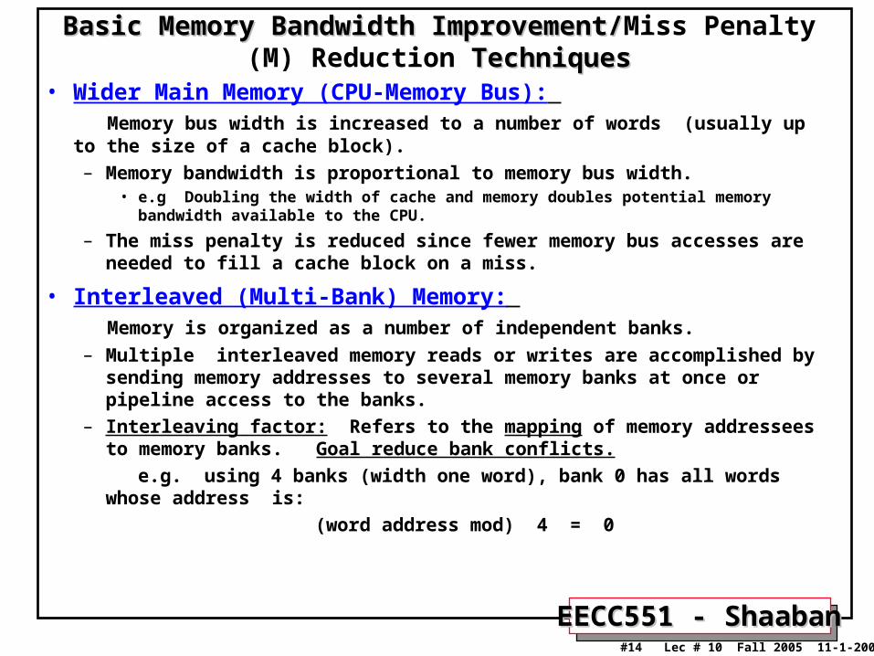
Basic Memory Bandwidth Improvement/Basic Memory Bandwidth Improvement/Miss Penalty (M) Reduction TechniquesTechniques
• Wider Main Memory (CPU-Memory Bus): Memory bus width is increased to a number of words (usually up to the size of a cache
block).– Memory bandwidth is proportional to memory bus width.
• e.g Doubling the width of cache and memory doubles potential memory bandwidth available to the CPU.
– The miss penalty is reduced since fewer memory bus accesses are needed to fill a cache block on a miss.
• Interleaved (Multi-Bank) Memory: Memory is organized as a number of independent banks.
– Multiple interleaved memory reads or writes are accomplished by sending memory addresses to several memory banks at once or pipeline access to the banks.
– Interleaving factor: Refers to the mapping of memory addressees to memory banks. Goal reduce bank conflicts.
e.g. using 4 banks (width one word), bank 0 has all words whose address is:
(word address mod) 4 = 0

EECC551 - ShaabanEECC551 - Shaaban#15 Lec # 10 Fall 2005 11-1-2005
Three examples of bus width, memory width, and memory interleaving to achieve higher memory bandwidth
Narrow busand cachewithinterleaved memorybanks
Wider memory, busand cache(highest performance)
Simplest design:Everything is the width of one word (lowest performance)
(FSB)
Front Side Bus (FSB) = System Bus = CPU-memory Bus
(FSB)

EECC551 - ShaabanEECC551 - Shaaban#16 Lec # 10 Fall 2005 11-1-2005
Four Way (Four Banks) Interleaved Memory
Memory Bank Number
Address WithinBank
048121620..
159131721..
2610141822..
3711151923..
Bank 0 Bank 1 Bank 2 Bank 3
Bank Width = One WordBank Number = (Word Address) Mod (4)

EECC551 - ShaabanEECC551 - Shaaban#17 Lec # 10 Fall 2005 11-1-2005
Memory Bank InterleavingMemory Bank Interleaving
Number of banks Number of cycles to access word in a bank
(One Memory Bank)
(4 banks similar to the organizationof DDR SDRAM memory chips)
Memory Bank Cycle Time
Memory Bank Cycle Time
Pipeline access to different memory banks to increase effective bandwidth
Can be applied at: 1- DRAM chip level (e.g SDRAM, DDR) 2- DRAM module level 3- DRAM channel level
Bank interleavingBank interleaving does not reduce latency of accesses to the same bank
Very long memory bank recovery time shown here

EECC551 - ShaabanEECC551 - Shaaban#18 Lec # 10 Fall 2005 11-1-2005
Synchronous DRAM Characteristics Summary
# of Banks per DRAM Chip
Bus Width Bytes
2 4 4 32
8 8 8 2
SDRAM DDR (Double Data Rate) SDRAM RAMbus
(Mid 2004)
(Similar to PC3200)
The latencies given only account for memory module latency and do not include memory controller latency or other address/data line delays. Thus realistic access latency is longer
.1 x 8 = .8 .133 x 2 x 8 = 2.1 .4 x 2 x 2 = 1.6.2 x2x 8 = 3.2
Peak Bandwidth(Latency not taken into account)
DRAMClockRate

EECC551 - ShaabanEECC551 - Shaaban#19 Lec # 10 Fall 2005 11-1-2005
SynchronousSynchronousDynamic RAM,Dynamic RAM,(SDRAM)(SDRAM)OrganizationOrganization
DDR SDRAM organization is similar but four banks are used in each DDR SDRAM chip instead of two.
Data transfer on both rising and falling edges of the clock
DDR SDRAM rated by maximum or peak memory bandwidthPC3200 = 8 bytes x 200 MHz x 2 = 3200 Mbytes/sec
(mid 90s)
(late 90s - current)
SDRAM speed is rated at max.clock speed supported:100MHZ = PC100133MHZ = PC133
A
SDRAM Peak Memory Bandwidth = = Bus Width /(0.5 x tCAC) = Bus Width x Clock rate
DDR SDRAM Peak Memory Bandwidth = = Bus Width /(0.25 x tCAC) = Bus Width x Clock rate x 2
(Data Lines)
AddressLines

EECC551 - ShaabanEECC551 - Shaaban#20 Lec # 10 Fall 2005 11-1-2005
Simplified SDRAM/DDR SDRAM Read TimingSimplified SDRAM/DDR SDRAM Read Timing
SDRAM Typical timing at 133 MHz (PC133 SDRAM) : 5-1-1-1 For bus width = 64 bits = 8 bytes Max. Bandwidth = 133 x 8 = 1064 Mbytes/sec It takes = 5+1+1+1 = 8 memory cycles or 7.5 ns x 8 = 60 ns to read 32 byte cache block Minimum Read Miss penalty for CPU running at 1 GHz = M = 7.5 x 8 = 60 CPU cycles
SDRAM(mid 90s)
Data Data Data Data Data Data Data DataDDR SDRAM(Late 90s-Now)
Latency (memory access time)
DDR SDRAM: Possible timing at 133 MHz (DDR x2) (PC2100 DDR SDRAM) : 5 - .5- .5- .5For bus width = 64 bits = 8 bytes Max. Bandwidth = 133 x 2 x 8 = 2128 Mbytes/secIt takes = 5+ .5 +.5 +.5 = 6.5 memory cycles or 7.5 ns x 8 = 45 ns to read 32 byte cache blockMinimum Read Miss penalty for CPU running at 1 GHz = M = 7.5 x 6 = 49 CPU cycles
(SDRAM Max. Burst Length = 8)
(DDR SDRAM Max. Burst Length = 16)
In this example for SDRAM: M = 60 cycles for DDR SDRAM: M = 49 cyclesThus accounting for access latency DDR is 60/49 = 1.22 times fasterNot twice as fast (2128/1064 = 2) as indicated by peak bandwidth!
Twice asfast asSDRAM?
SDRAM clock cycle time ~ ½ tCAC

EECC551 - ShaabanEECC551 - Shaaban#21 Lec # 10 Fall 2005 11-1-2005
Block Size (bytes)
Miss Rate
0%
5%
10%
15%
20%
25%
16
32
64
12
8
25
6
1K
4K
16K
64K
256K
The Impact of Larger Cache Block Size on Miss RateThe Impact of Larger Cache Block Size on Miss Rate• A larger cache block size improves cache performance by taking better advantage of spatial locality However, for a fixed cache size, larger block sizes mean fewer cache block frames •
• Performance keeps improving to a limit when the fewer number of cache block frames increases conflicts and thus overall cache miss rate
For SPEC92
Improves spatial locality reducing compulsory misses
X

EECC551 - ShaabanEECC551 - Shaaban#22 Lec # 10 Fall 2005 11-1-2005
Memory Width, Interleaving: Performance ExampleMemory Width, Interleaving: Performance ExampleGiven the following system parameters with single unified cache level L1 (ignoring write policy):
Block size= 1 word Memory bus width= 1 word Miss rate =3% M = Miss penalty = 32 cycles
(4 cycles to send address 24 cycles access time, 4 cycles to send a word to CPU)
Memory access/instruction = 1.2 CPIexecution (ignoring cache misses) = 2
Miss rate (block size = 2 word = 8 bytes ) = 2% Miss rate (block size = 4 words = 16 bytes) = 1%
• The CPI of the base machine with 1-word blocks = 2 + (1.2 x 0.03 x 32) = 3.15
Increasing the block size to two words (64 bits) gives the following CPI: (miss rate = 2%)
• 32-bit bus and memory, no interleaving, M = 2 x 32 = 64 cycles CPI = 2 + (1.2 x .02 x 64) = 3.54
• 32-bit bus and memory, interleaved, M = 4 + 24 + 8 = 36 cycles CPI = 2 + (1.2 x .02 x 36) = 2.86
• 64-bit bus and memory, no interleaving, M = 32 cycles CPI = 2 + (1.2 x 0.02 x 32) = 2.77
Increasing the block size to four words (128 bits); resulting CPI: (miss rate = 1%)
• 32-bit bus and memory, no interleaving , M = 4 x 32 = 128 cycles CPI = 2 + (1.2 x 0.01 x 128) = 3.54
• 32-bit bus and memory, interleaved , M = 4 + 24 + 16 = 44 cycles CPI = 2 + (1.2 x 0.01 x 44) = 2.53
• 64-bit bus and memory, no interleaving, M = 2 x 32 = 64 cycles CPI = 2 + (1.2 x 0.01 x 64) = 2.77
• 64-bit bus and memory, interleaved, M = 4 + 24 + 8 = 36 cycles CPI = 2 + (1.2 x 0.01 x 36) = 2.43
• 128-bit bus and memory, no interleaving, M = 32 cycles CPI = 2 + (1.2 x 0.01 x 32) = 2.38
4 cycles 24 cycles 4 cycles Miss Penalty = M= 4 + 24 + 4 = 32 cycles
Miss Penalty = M = Number of CPU stall cycles for an access missed in cache and satisfied by main memory
(Base system)
(For Base system)
EECC551 - ShaabanEECC551 - Shaaban#23 Lec # 10 Fall 2005 11-1-2005
Repeated here from lecture 8
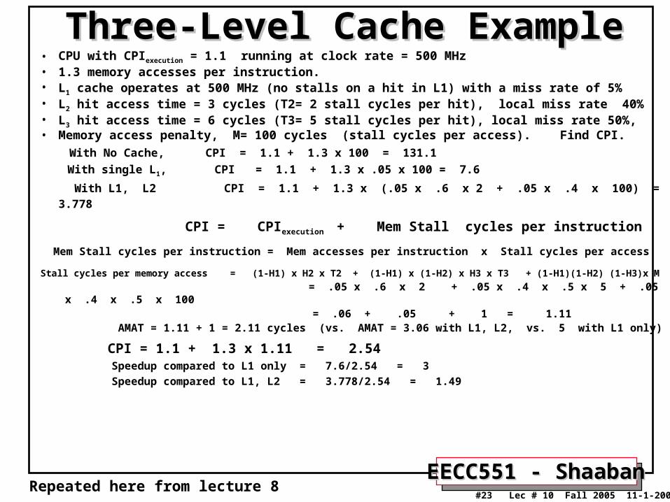
Three-Level Cache ExampleThree-Level Cache Example• CPU with CPIexecution = 1.1 running at clock rate = 500 MHz• 1.3 memory accesses per instruction.• L1 cache operates at 500 MHz (no stalls on a hit in L1) with a miss rate of 5%• L2 hit access time = 3 cycles (T2= 2 stall cycles per hit), local miss rate 40%• L3 hit access time = 6 cycles (T3= 5 stall cycles per hit), local miss rate 50%, • Memory access penalty, M= 100 cycles (stall cycles per access). Find CPI.
With No Cache, CPI = 1.1 + 1.3 x 100 = 131.1
With single L1, CPI = 1.1 + 1.3 x .05 x 100 = 7.6
With L1, L2 CPI = 1.1 + 1.3 x (.05 x .6 x 2 + .05 x .4 x 100) = 3.778
CPI = CPIexecution + Mem Stall cycles per instruction
Mem Stall cycles per instruction = Mem accesses per instruction x Stall cycles per access
Stall cycles per memory access = (1-H1) x H2 x T2 + (1-H1) x (1-H2) x H3 x T3 + (1-H1)(1-H2) (1-H3)x M
= .05 x .6 x 2 + .05 x .4 x .5 x 5 + .05 x .4 x .5 x 100 = .06 + .05 + 1 = 1.11 AMAT = 1.11 + 1 = 2.11 cycles (vs. AMAT = 3.06 with L1, L2, vs. 5 with L1 only)
CPI = 1.1 + 1.3 x 1.11 = 2.54 Speedup compared to L1 only = 7.6/2.54 = 3
Speedup compared to L1, L2 = 3.778/2.54 = 1.49

EECC551 - ShaabanEECC551 - Shaaban#24 Lec # 10 Fall 2005 11-1-2005
L1 Miss, L2 Miss, L3 Hit:Hit Access Time =T3 +1 = 6Stalls per L2 Hit = T3 = 5
Stalls = (1-H1) x (1-H2) x H3 x T3 = .01 x 5 = .05 cycles
Stall cycles per memory access = (1-H1) x H2 x T2 + (1-H1) x (1-H2) x H3 x T3 + (1-H1)(1-H2) (1-H3)x M = .06 + .05 +1 = 1.11AMAT = 1 + Stall cycles per memory access = 1 + 1.11 = 2.11 cycles
Repeated here from lecture 8 with values for example added
3-Level (All Unified) Cache Performance3-Level (All Unified) Cache Performance Memory Access Tree (Ignoring Write Policy) Memory Access Tree (Ignoring Write Policy)
CPU Stall Cycles Per Memory AccessCPU Stall Cycles Per Memory Access
CPU Memory Access
L1 Miss: % = (1-H1) = .05 or 5%
L1 Hit:Hit Access Time = 1Stalls Per access = 0Stalls= H1 x 0 = 0 ( No Stall)
L1 Miss, L2 Miss: % = (1-H1)(1-H2) = .05 x .4 = .02 or 2%
L1 Miss, L2 Hit:Hit Access Time =T2 +1 = 3Stalls per L2 Hit = T2 =2Stalls =(1-H1) x H2 x T2 = .05 x .6 x 2 = .06
L1 Miss, L2, Miss, L3 Miss: Miss Penalty = M = 100Stalls = (1-H1)(1-H2)(1-H3) x M = .01 x 100 = 1 cycle
L1
L3
L2
T2 = 2 cycles = Stalls per hit access for Level 2T3 = 5 cycles = Stalls per hit access for Level 3
M= Memory Miss Penalty = M = 100 cycles
(1-H1) x (1-H2) x H3 = .05 x .4 x .5 = .01 or 1%
(1-H1)(1-H2)(1-H3) = .05 x .4 x .5 = .01 or 1%
H1 = .95 or 95%
(1-H1) x H2= .05 x .6= .03 or 3%
(100%)
H1 = 95% T1 = 0 cyclesH2 = 60% T2 = 2 cyclesH3 = 50% T3 = 5 cycles
M = 100 cyclesStalls on a hit
CPI = CPIexecution + (1 + fraction of loads and stores) x stalls per accessCPI = 1.1 + 1.3 x 1.11 = 2.54

EECC551 - ShaabanEECC551 - Shaaban#25 Lec # 10 Fall 2005 11-1-2005
Program Steady-State Main Memory Bandwidth-Usage ExampleProgram Steady-State Main Memory Bandwidth-Usage Example• In the previous example with three levels of cache (all unified, ignore write policy)• CPU with CPIexecution = 1.1 running at clock rate = 500 MHz• 1.3 memory accesses per instruction.• L1 cache operates at 500 MHz (no stalls on a hit in L1) with a miss rate of 5%• L2 hit access time = 3 cycles (T2= 2 stall cycles per hit), local miss rate 40%• L3 hit access time = 6 cycles (T3= 5 stall cycles per hit), local miss rate 50%, • Memory access penalty, M= 100 cycles (stall cycles per access to deliver 32 bytes from main memory to CPU)
• We found the CPI:
With No Cache, CPI = 1.1 + 1.3 x 100 = 131.1
With single L1, CPI = 1.1 + 1.3 x .05 x 100 = 7.6
With L1, L2 CPI = 1.1 + 1.3 x (.05 x .6 x 2 + .05 x .4 x 100) = 3.778
With L1, L2 , L3 CPI = 1.1 + 1.3 x 1.11 = 2.54
Assuming:
All cache blocks are 32 bytes
For each of the three cases with cache:
What is the total number of memory accesses generated by the CPU per second?
What is the percentage of these memory accesses satisfied by main memory?
Percentage of main memory bandwidth used by the CPU?

EECC551 - ShaabanEECC551 - Shaaban#26 Lec # 10 Fall 2005 11-1-2005
• Memory requires 100 CPU cycles = 200 ns to deliver 32 bytes, thus total main memory effective bandwidth = 32 bytes / (200 ns) = 160 x 106 bytes/sec
• The total number of memory accesses generated by the CPU per second = (memory access/instruction) x clock rate / CPI = 1.3 x 500 x 106 / CPI = 650 x 106 / CPI
– With single L1 = 650 x 106 / 7.6 = 85 x 106 accesses/sec
– With L1, L2 = 650 x 106 / 3.778 = 172 x 106 accesses/sec
– With L1, L2, L3 = 650 x 106 / 2.54 = 255 x 106 accesses/sec • The percentage of these memory accesses satisfied by main memory:
– With single L1 = L1 miss rate = 5%
– With L1, L2 = L1 miss rate x L2 miss rate = .05 x .4 = 2%
– with L1, L2, L3 = L1 miss rate x L2 miss rate x L3 miss rate = .05 x .4 x . 5 = 1%• Memory Bandwidth used
– With single L1 = 32 bytes x 85x106 accesses/sec x .05 = 136 x106 bytes/sec
or 136/160 = 85 % of total memory bandwidth
– With L1, L2 = 32 bytes x 172 x106 accesses/sec x .02 = 110 x106 bytes/sec
or 110/160 = 69 % of total memory bandwidth
– With L1, L2, L3 = 32 bytes x 255 x106 accesses/sec x .01 = 82 x106 bytes/sec
or 82/160 = 51 % of total memory bandwidth
Program Steady-State Main Memory Bandwidth-Usage ExampleProgram Steady-State Main Memory Bandwidth-Usage Example
Similarly the percentage of CPU memory accesses satisfied by a cache level and percentage of bandwidth used for each cache level can be estimated

EECC551 - ShaabanEECC551 - Shaaban#27 Lec # 10 Fall 2005 11-1-2005
X86 CPU Dual Channel PC3200 DDR SDRAM
Sample (Realistic?) Bandwidth Data
Source: The Tech Report 1-21-2004http://www.tech-report.com/reviews/2004q1/athlon64-3000/index.x?pg=3
Dual (64-bit) Channel PC3200 DDR SDRAMhas a theoretical peak bandwidth of
400 MHz x 8 bytes x 2 = 6400 MB/s
Is memory bandwidth still an issue?

EECC551 - ShaabanEECC551 - Shaaban#28 Lec # 10 Fall 2005 11-1-2005
X86 CPU Dual Channel PC3200 DDR SDRAM
Sample (Realistic?) Latency Data
2.2GHz
On-ChipMemory ControllerLowers EffectiveMemory Latency
(256 CPU Cycles)
(104 CPU Cycles)
Source: The Tech Report (1-21-2004)http://www.tech-report.com/reviews/2004q1/athlon64-3000/index.x?pg=3
PC3200 DDR SDRAMhas a theoretical latency range of 18-40 ns (not accounting for memory controller latency or other address/data line delays).
Is memory latency still an issue?

EECC551 - ShaabanEECC551 - Shaaban#29 Lec # 10 Fall 2005 11-1-2005
X86 CPU Cache/Memory Performance Example:X86 CPU Cache/Memory Performance Example:AMD Athlon XP/64/FX Vs. Intel P4/Extreme EditionAMD Athlon XP/64/FX Vs. Intel P4/Extreme Edition
Main Memory: Dual (64-bit) Channel PC3200 DDR SDRAMpeak bandwidth of 6400 MB/s
Intel P4 3.2 GHzExtreme EditionData L1: 8KBData L2: 512 KBData L3: 2048 KB
Intel P4 3.2 GHzData L1: 8KBData L2: 512 KB
AMD Athon XP 2.2 GHzData L1: 64KBData L2: 512 KB (exclusive)
Source: The Tech Report 1-21-2004http://www.tech-report.com/reviews/2004q1/athlon64-3000/index.x?pg=3
AMD Athon 64 FX51 2.2 GHzData L1: 64KBData L2: 1024 KB (exlusive)
AMD Athon 64 3400+ 2.2 GHzData L1: 64KBData L2: 1024 KB (exclusive)
AMD Athon 64 3000+ 2.0 GHzData L1: 64KBData L2: 512 KB (exclusive)
AMD Athon 64 3200+ 2.0 GHzData L1: 64KBData L2: 1024 KB (exclusive)