DS90CR486 133MHz 48-Bit Channel Link Deserializer … SNLS149C – FEBRUARY 2003– REVISED MARCH...
22
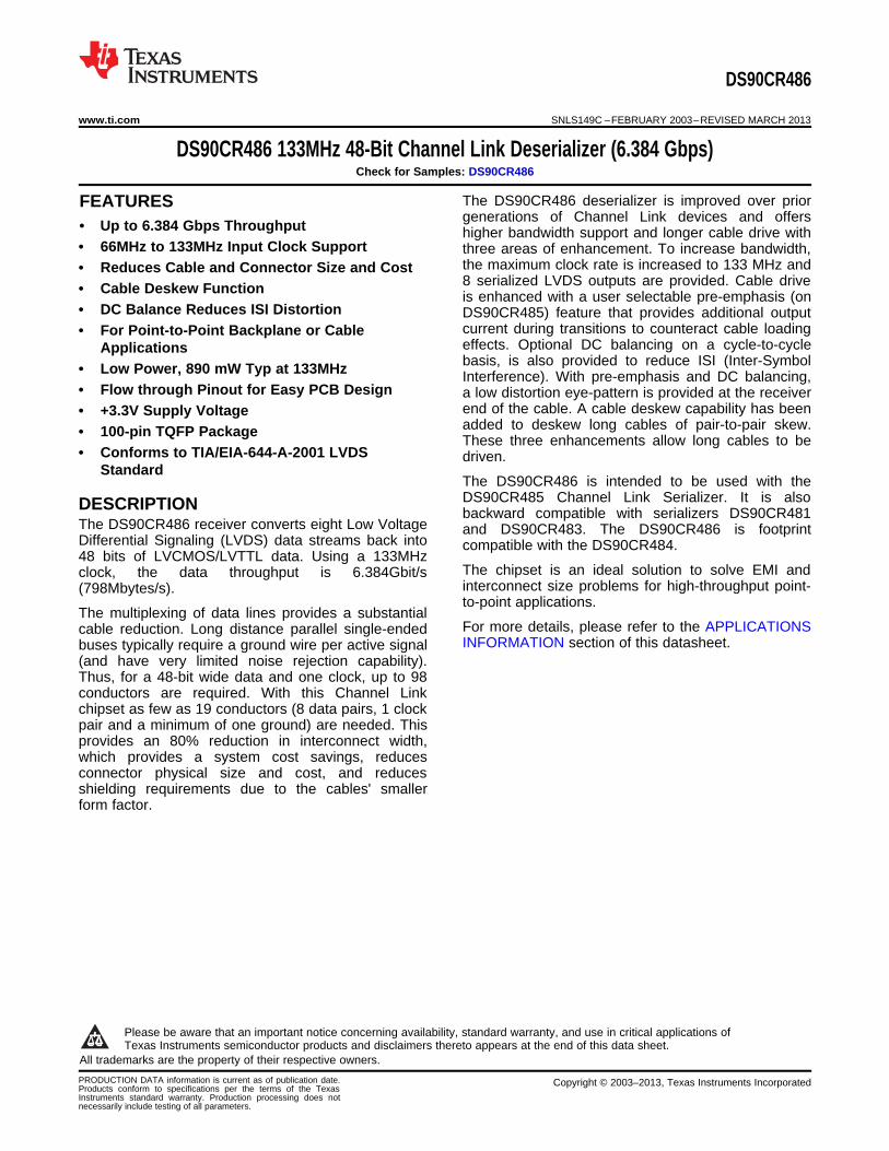
DS90CR486 www.ti.com SNLS149C – FEBRUARY 2003 – REVISED MARCH 2013 DS90CR486 133MHz 48-Bit Channel Link Deserializer (6.384 Gbps) Check for Samples: DS90CR486 The DS90CR486 deserializer is improved over prior 1FEATURES generations of Channel Link devices and offers 2• Up to 6.384 Gbps Throughput higher bandwidth support and longer cable drive with • 66MHz to 133MHz Input Clock Support three areas of enhancement. To increase bandwidth, the maximum clock rate is increased to 133 MHz and • Reduces Cable and Connector Size and Cost 8 serialized LVDS outputs are provided. Cable drive • Cable Deskew Function is enhanced with a user selectable pre-emphasis (on • DC Balance Reduces ISI Distortion DS90CR485) feature that provides additional output current during transitions to counteract cable loading • For Point-to-Point Backplane or Cable effects. Optional DC balancing on a cycle-to-cycle Applications basis, is also provided to reduce ISI (Inter-Symbol • Low Power, 890 mW Typ at 133MHz Interference). With pre-emphasis and DC balancing, • Flow through Pinout for Easy PCB Design a low distortion eye-pattern is provided at the receiver end of the cable. A cable deskew capability has been • +3.3V Supply Voltage added to deskew long cables of pair-to-pair skew. • 100-pin TQFP Package These three enhancements allow long cables to be • Conforms to TIA/EIA-644-A-2001 LVDS driven. Standard The DS90CR486 is intended to be used with the DS90CR485 Channel Link Serializer. It is also DESCRIPTION backward compatible with serializers DS90CR481 The DS90CR486 receiver converts eight Low Voltage and DS90CR483. The DS90CR486 is footprint Differential Signaling (LVDS) data streams back into compatible with the DS90CR484. 48 bits of LVCMOS/LVTTL data. Using a 133MHz The chipset is an ideal solution to solve EMI and clock, the data throughput is 6.384Gbit/s interconnect size problems for high-throughput point- (798Mbytes/s). to-point applications. The multiplexing of data lines provides a substantial For more details, please refer to the APPLICATIONS cable reduction. Long distance parallel single-ended INFORMATION section of this datasheet. buses typically require a ground wire per active signal (and have very limited noise rejection capability). Thus, for a 48-bit wide data and one clock, up to 98 conductors are required. With this Channel Link chipset as few as 19 conductors (8 data pairs, 1 clock pair and a minimum of one ground) are needed. This provides an 80% reduction in interconnect width, which provides a system cost savings, reduces connector physical size and cost, and reduces shielding requirements due to the cables' smaller form factor. 1 Please be aware that an important notice concerning availability, standard warranty, and use in critical applications of Texas Instruments semiconductor products and disclaimers thereto appears at the end of this data sheet. 2All trademarks are the property of their respective owners. PRODUCTION DATA information is current as of publication date. Copyright © 2003–2013, Texas Instruments Incorporated Products conform to specifications per the terms of the Texas Instruments standard warranty. Production processing does not necessarily include testing of all parameters.
Transcript of DS90CR486 133MHz 48-Bit Channel Link Deserializer … SNLS149C – FEBRUARY 2003– REVISED MARCH...
DS90CR486
www.ti.com SNLS149C –FEBRUARY 2003–REVISED MARCH 2013
DS90CR486 133MHz 48-Bit Channel Link Deserializer (6.384 Gbps)Check for Samples: DS90CR486
The DS90CR486 deserializer is improved over prior1FEATURES
generations of Channel Link devices and offers2• Up to 6.384 Gbps Throughput higher bandwidth support and longer cable drive with• 66MHz to 133MHz Input Clock Support three areas of enhancement. To increase bandwidth,
the maximum clock rate is increased to 133 MHz and• Reduces Cable and Connector Size and Cost8 serialized LVDS outputs are provided. Cable drive• Cable Deskew Function is enhanced with a user selectable pre-emphasis (on
• DC Balance Reduces ISI Distortion DS90CR485) feature that provides additional outputcurrent during transitions to counteract cable loading• For Point-to-Point Backplane or Cableeffects. Optional DC balancing on a cycle-to-cycleApplicationsbasis, is also provided to reduce ISI (Inter-Symbol• Low Power, 890 mW Typ at 133MHz Interference). With pre-emphasis and DC balancing,
• Flow through Pinout for Easy PCB Design a low distortion eye-pattern is provided at the receiverend of the cable. A cable deskew capability has been• +3.3V Supply Voltageadded to deskew long cables of pair-to-pair skew.• 100-pin TQFP PackageThese three enhancements allow long cables to be
• Conforms to TIA/EIA-644-A-2001 LVDS driven.Standard
The DS90CR486 is intended to be used with theDS90CR485 Channel Link Serializer. It is alsoDESCRIPTIONbackward compatible with serializers DS90CR481
The DS90CR486 receiver converts eight Low Voltage and DS90CR483. The DS90CR486 is footprintDifferential Signaling (LVDS) data streams back into compatible with the DS90CR484.48 bits of LVCMOS/LVTTL data. Using a 133MHz
The chipset is an ideal solution to solve EMI andclock, the data throughput is 6.384Gbit/sinterconnect size problems for high-throughput point-(798Mbytes/s).to-point applications.
The multiplexing of data lines provides a substantialFor more details, please refer to the APPLICATIONScable reduction. Long distance parallel single-endedINFORMATION section of this datasheet.buses typically require a ground wire per active signal
(and have very limited noise rejection capability).Thus, for a 48-bit wide data and one clock, up to 98conductors are required. With this Channel Linkchipset as few as 19 conductors (8 data pairs, 1 clockpair and a minimum of one ground) are needed. Thisprovides an 80% reduction in interconnect width,which provides a system cost savings, reducesconnector physical size and cost, and reducesshielding requirements due to the cables' smallerform factor.
1
Please be aware that an important notice concerning availability, standard warranty, and use in critical applications ofTexas Instruments semiconductor products and disclaimers thereto appears at the end of this data sheet.
2All trademarks are the property of their respective owners.
PRODUCTION DATA information is current as of publication date. Copyright © 2003–2013, Texas Instruments IncorporatedProducts conform to specifications per the terms of the TexasInstruments standard warranty. Production processing does notnecessarily include testing of all parameters.

DS90CR486
SNLS149C –FEBRUARY 2003–REVISED MARCH 2013 www.ti.com
Generalized Block Diagram
These devices have limited built-in ESD protection. The leads should be shorted together or the device placed in conductive foamduring storage or handling to prevent electrostatic damage to the MOS gates.
Absolute Maximum Ratings (1) (2)
Value Unit
Supply Voltage (VCC) −0.3 to +3.6 V
LVCMOS/LVTTL Output Voltage −0.3 to (VCC + 0.3) V
LVDS Receiver Input Voltage −0.3 to +3.6 V
Junction Temperature +150 °C
Storage Temperature −65 to +150 °C
Lead Temperature (Soldering, 4 sec.) +260 °C
Maximum Package Power Dissipation Capacity @ 25°C 100 TQFP Package: 2.9 W
Package Derating: 23.8 mW/°C above +25°C
ESD Rating: (HBM, 1.5kΩ, 100pF) > 2 kV
ESD Rating: (EIAJ, 0Ω, 200pF) > 200 V
(1) “Absolute Maximum Ratings” are those values beyond which the safety of the device cannot be ensured. They are not meant to implythat the device should be operated at these limits. “Electrical Characteristics” specify conditions for device operation.
(2) If Military/Aerospace specified devices are required, please contact the Texas Instruments Sales Office/ Distributors for availability andspecifications.
Recommended Operating ConditionsMin Nom Max Units
Supply Voltage (VCC) 3.14 3.3 3.46 V
Operating Free Air Temperature (TA) −10 +25 +70 °C
Receiver Input Range 0 2.4 V
Supply Noise Voltage (VCC) 100 mVp-p
Clock Rate 66 133 MHz
2 Submit Documentation Feedback Copyright © 2003–2013, Texas Instruments Incorporated
Product Folder Links: DS90CR486
DS90CR486
www.ti.com SNLS149C –FEBRUARY 2003–REVISED MARCH 2013
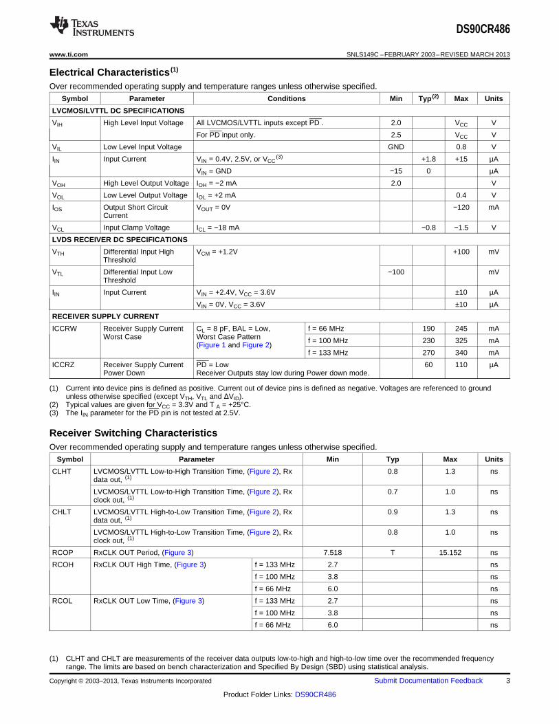
Electrical Characteristics (1)
Over recommended operating supply and temperature ranges unless otherwise specified.
Symbol Parameter Conditions Min Typ (2) Max Units
LVCMOS/LVTTL DC SPECIFICATIONS
VIH High Level Input Voltage All LVCMOS/LVTTL inputs except PD . 2.0 VCC V
For PD input only. 2.5 VCC V
VIL Low Level Input Voltage GND 0.8 V
IIN Input Current VIN = 0.4V, 2.5V, or VCC(3) +1.8 +15 µA
VIN = GND −15 0 µA
VOH High Level Output Voltage IOH = −2 mA 2.0 V
VOL Low Level Output Voltage IOL = +2 mA 0.4 V
IOS Output Short Circuit VOUT = 0V −120 mACurrent
VCL Input Clamp Voltage ICL = −18 mA −0.8 −1.5 V
LVDS RECEIVER DC SPECIFICATIONS
VTH Differential Input High VCM = +1.2V +100 mVThreshold
VTL Differential Input Low −100 mVThreshold
IIN Input Current VIN = +2.4V, VCC = 3.6V ±10 µA
VIN = 0V, VCC = 3.6V ±10 µA
RECEIVER SUPPLY CURRENT
ICCRW Receiver Supply Current CL = 8 pF, BAL = Low, f = 66 MHz 190 245 mAWorst Case Worst Case Pattern f = 100 MHz 230 325 mA
(Figure 1 and Figure 2)f = 133 MHz 270 340 mA
ICCRZ Receiver Supply Current PD = Low 60 110 µAPower Down Receiver Outputs stay low during Power down mode.
(1) Current into device pins is defined as positive. Current out of device pins is defined as negative. Voltages are referenced to groundunless otherwise specified (except VTH, VTL and ΔVID).
(2) Typical values are given for VCC = 3.3V and T A = +25°C.(3) The IIN parameter for the PD pin is not tested at 2.5V.
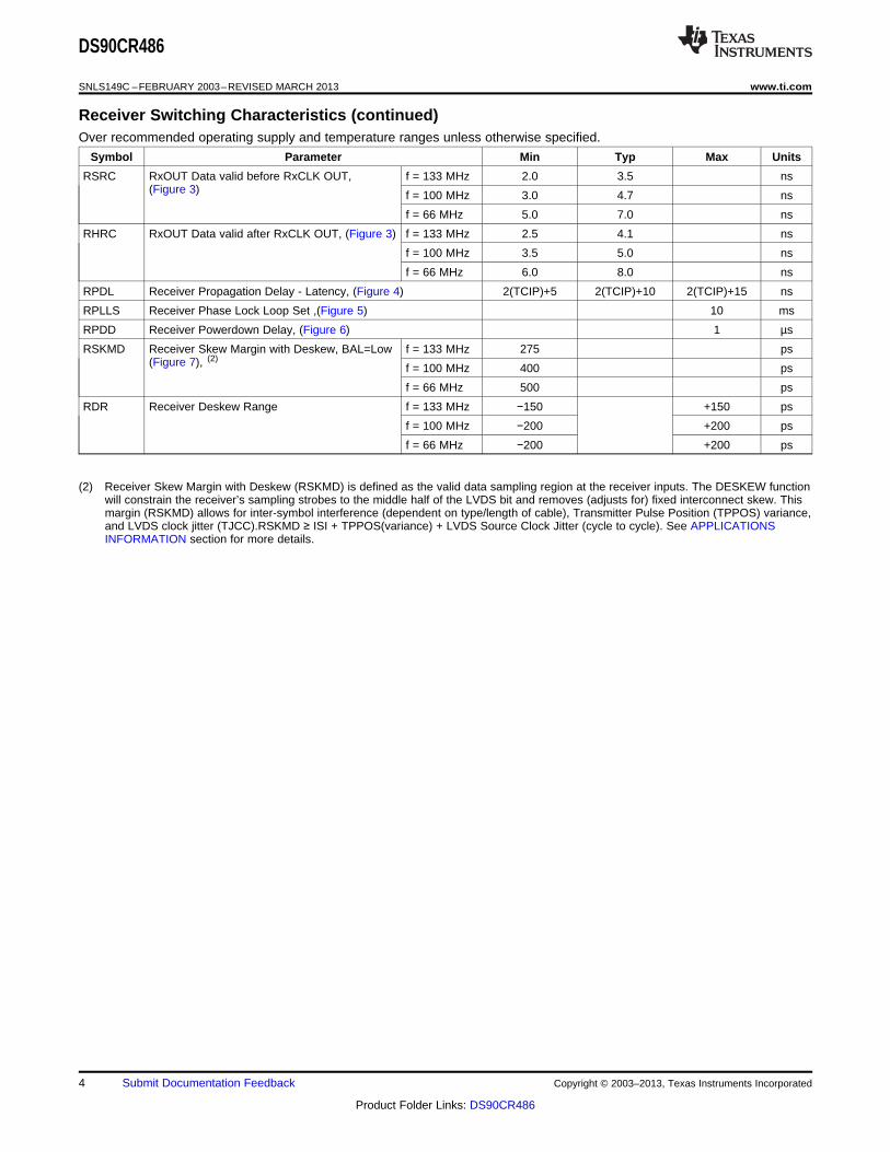
Receiver Switching CharacteristicsOver recommended operating supply and temperature ranges unless otherwise specified.
Symbol Parameter Min Typ Max Units
CLHT LVCMOS/LVTTL Low-to-High Transition Time, (Figure 2), Rx 0.8 1.3 nsdata out, (1)
LVCMOS/LVTTL Low-to-High Transition Time, (Figure 2), Rx 0.7 1.0 nsclock out, (1)
CHLT LVCMOS/LVTTL High-to-Low Transition Time, (Figure 2), Rx 0.9 1.3 nsdata out, (1)
LVCMOS/LVTTL High-to-Low Transition Time, (Figure 2), Rx 0.8 1.0 nsclock out, (1)
RCOP RxCLK OUT Period, (Figure 3) 7.518 T 15.152 ns
RCOH RxCLK OUT High Time, (Figure 3) f = 133 MHz 2.7 ns
f = 100 MHz 3.8 ns
f = 66 MHz 6.0 ns
RCOL RxCLK OUT Low Time, (Figure 3) f = 133 MHz 2.7 ns
f = 100 MHz 3.8 ns
f = 66 MHz 6.0 ns
(1) CLHT and CHLT are measurements of the receiver data outputs low-to-high and high-to-low time over the recommended frequencyrange. The limits are based on bench characterization and Specified By Design (SBD) using statistical analysis.
Copyright © 2003–2013, Texas Instruments Incorporated Submit Documentation Feedback 3
Product Folder Links: DS90CR486
DS90CR486
SNLS149C –FEBRUARY 2003–REVISED MARCH 2013 www.ti.com
Receiver Switching Characteristics (continued)Over recommended operating supply and temperature ranges unless otherwise specified.
Symbol Parameter Min Typ Max Units
RSRC RxOUT Data valid before RxCLK OUT, f = 133 MHz 2.0 3.5 ns(Figure 3) f = 100 MHz 3.0 4.7 ns
f = 66 MHz 5.0 7.0 ns
RHRC RxOUT Data valid after RxCLK OUT, (Figure 3) f = 133 MHz 2.5 4.1 ns
f = 100 MHz 3.5 5.0 ns
f = 66 MHz 6.0 8.0 ns
RPDL Receiver Propagation Delay - Latency, (Figure 4) 2(TCIP)+5 2(TCIP)+10 2(TCIP)+15 ns
RPLLS Receiver Phase Lock Loop Set ,(Figure 5) 10 ms
RPDD Receiver Powerdown Delay, (Figure 6) 1 µs
RSKMD Receiver Skew Margin with Deskew, BAL=Low f = 133 MHz 275 ps(Figure 7), (2)
f = 100 MHz 400 ps
f = 66 MHz 500 ps
RDR Receiver Deskew Range f = 133 MHz −150 +150 ps
f = 100 MHz −200 +200 ps
f = 66 MHz −200 +200 ps
(2) Receiver Skew Margin with Deskew (RSKMD) is defined as the valid data sampling region at the receiver inputs. The DESKEW functionwill constrain the receiver’s sampling strobes to the middle half of the LVDS bit and removes (adjusts for) fixed interconnect skew. Thismargin (RSKMD) allows for inter-symbol interference (dependent on type/length of cable), Transmitter Pulse Position (TPPOS) variance,and LVDS clock jitter (TJCC).RSKMD ≥ ISI + TPPOS(variance) + LVDS Source Clock Jitter (cycle to cycle). See APPLICATIONSINFORMATION section for more details.
4 Submit Documentation Feedback Copyright © 2003–2013, Texas Instruments Incorporated
Product Folder Links: DS90CR486
DS90CR486
www.ti.com SNLS149C –FEBRUARY 2003–REVISED MARCH 2013
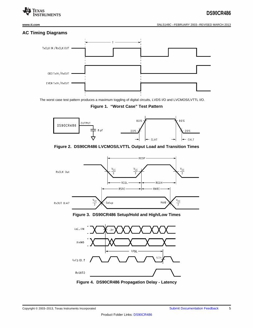
AC Timing Diagrams
The worst case test pattern produces a maximum toggling of digital circuits, LVDS I/O and LVCMOS/LVTTL I/O.
Figure 1. “Worst Case” Test Pattern
Figure 2. DS90CR486 LVCMOS/LVTTL Output Load and Transition Times
Figure 3. DS90CR486 Setup/Hold and High/Low Times
Figure 4. DS90CR486 Propagation Delay - Latency
Copyright © 2003–2013, Texas Instruments Incorporated Submit Documentation Feedback 5
Product Folder Links: DS90CR486
DS90CR486
SNLS149C –FEBRUARY 2003–REVISED MARCH 2013 www.ti.com
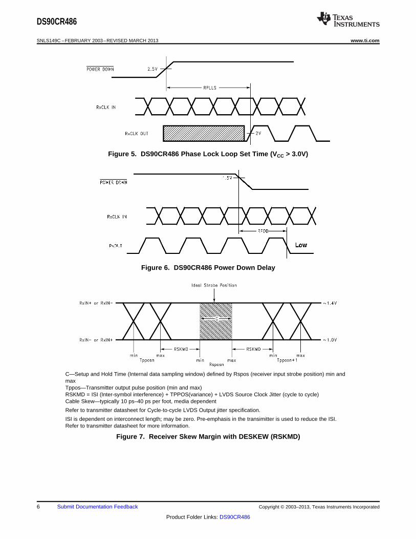
Figure 5. DS90CR486 Phase Lock Loop Set Time (VCC > 3.0V)
Figure 6. DS90CR486 Power Down Delay
C—Setup and Hold Time (Internal data sampling window) defined by Rspos (receiver input strobe position) min andmaxTppos—Transmitter output pulse position (min and max)RSKMD = ISI (Inter-symbol interference) + TPPOS(variance) + LVDS Source Clock Jitter (cycle to cycle)Cable Skew—typically 10 ps–40 ps per foot, media dependent
Refer to transmitter datasheet for Cycle-to-cycle LVDS Output jitter specification.
ISI is dependent on interconnect length; may be zero. Pre-emphasis in the transimitter is used to reduce the ISI.Refer to transmitter datasheet for more information.
Figure 7. Receiver Skew Margin with DESKEW (RSKMD)
6 Submit Documentation Feedback Copyright © 2003–2013, Texas Instruments Incorporated
Product Folder Links: DS90CR486
DS90CR486
www.ti.com SNLS149C –FEBRUARY 2003–REVISED MARCH 2013
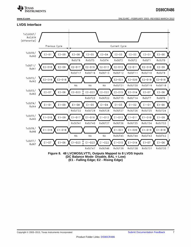
LVDS Interface
Figure 8. 48 LVCMOS/LVTTL Outputs Mapped to 8 LVDS Inputs(DC Balance Mode- Disable, BAL = Low)
(E1 - Falling Edge; E2 - Rising Edge)
Copyright © 2003–2013, Texas Instruments Incorporated Submit Documentation Feedback 7
Product Folder Links: DS90CR486
DS90CR486
SNLS149C –FEBRUARY 2003–REVISED MARCH 2013 www.ti.com
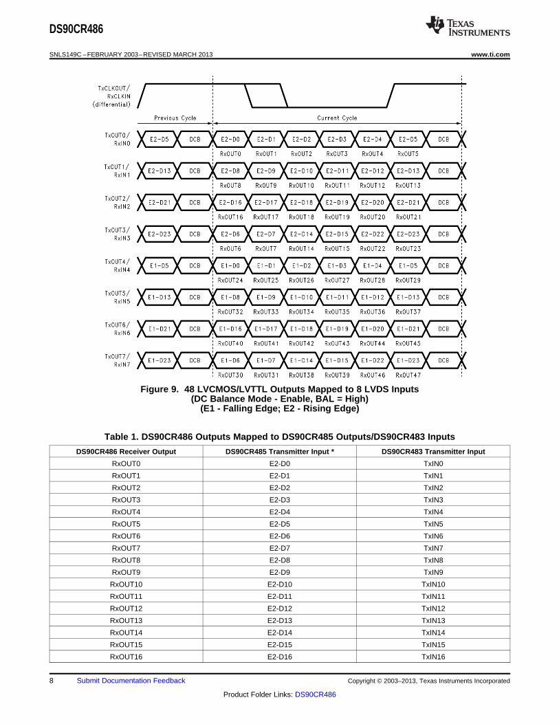
Figure 9. 48 LVCMOS/LVTTL Outputs Mapped to 8 LVDS Inputs(DC Balance Mode - Enable, BAL = High)
(E1 - Falling Edge; E2 - Rising Edge)
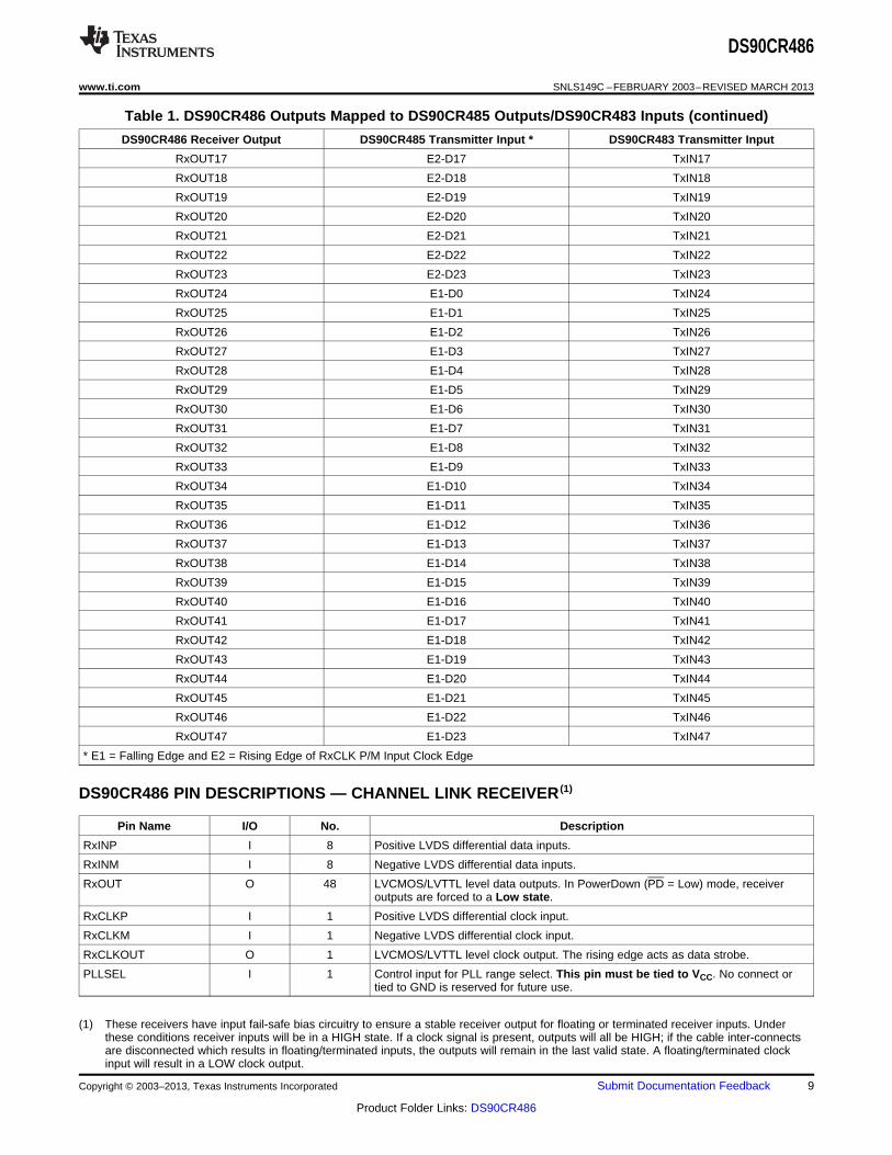
Table 1. DS90CR486 Outputs Mapped to DS90CR485 Outputs/DS90CR483 Inputs
DS90CR486 Receiver Output DS90CR485 Transmitter Input * DS90CR483 Transmitter Input
RxOUT0 E2-D0 TxIN0
RxOUT1 E2-D1 TxIN1
RxOUT2 E2-D2 TxIN2
RxOUT3 E2-D3 TxIN3
RxOUT4 E2-D4 TxIN4
RxOUT5 E2-D5 TxIN5
RxOUT6 E2-D6 TxIN6
RxOUT7 E2-D7 TxIN7
RxOUT8 E2-D8 TxIN8
RxOUT9 E2-D9 TxIN9
RxOUT10 E2-D10 TxIN10
RxOUT11 E2-D11 TxIN11
RxOUT12 E2-D12 TxIN12
RxOUT13 E2-D13 TxIN13
RxOUT14 E2-D14 TxIN14
RxOUT15 E2-D15 TxIN15
RxOUT16 E2-D16 TxIN16
8 Submit Documentation Feedback Copyright © 2003–2013, Texas Instruments Incorporated
Product Folder Links: DS90CR486
DS90CR486
www.ti.com SNLS149C –FEBRUARY 2003–REVISED MARCH 2013
Table 1. DS90CR486 Outputs Mapped to DS90CR485 Outputs/DS90CR483 Inputs (continued)
DS90CR486 Receiver Output DS90CR485 Transmitter Input * DS90CR483 Transmitter Input
RxOUT17 E2-D17 TxIN17
RxOUT18 E2-D18 TxIN18
RxOUT19 E2-D19 TxIN19
RxOUT20 E2-D20 TxIN20
RxOUT21 E2-D21 TxIN21
RxOUT22 E2-D22 TxIN22
RxOUT23 E2-D23 TxIN23
RxOUT24 E1-D0 TxIN24
RxOUT25 E1-D1 TxIN25
RxOUT26 E1-D2 TxIN26
RxOUT27 E1-D3 TxIN27
RxOUT28 E1-D4 TxIN28
RxOUT29 E1-D5 TxIN29
RxOUT30 E1-D6 TxIN30
RxOUT31 E1-D7 TxIN31
RxOUT32 E1-D8 TxIN32
RxOUT33 E1-D9 TxIN33
RxOUT34 E1-D10 TxIN34
RxOUT35 E1-D11 TxIN35
RxOUT36 E1-D12 TxIN36
RxOUT37 E1-D13 TxIN37
RxOUT38 E1-D14 TxIN38
RxOUT39 E1-D15 TxIN39
RxOUT40 E1-D16 TxIN40
RxOUT41 E1-D17 TxIN41
RxOUT42 E1-D18 TxIN42
RxOUT43 E1-D19 TxIN43
RxOUT44 E1-D20 TxIN44
RxOUT45 E1-D21 TxIN45
RxOUT46 E1-D22 TxIN46
RxOUT47 E1-D23 TxIN47
* E1 = Falling Edge and E2 = Rising Edge of RxCLK P/M Input Clock Edge
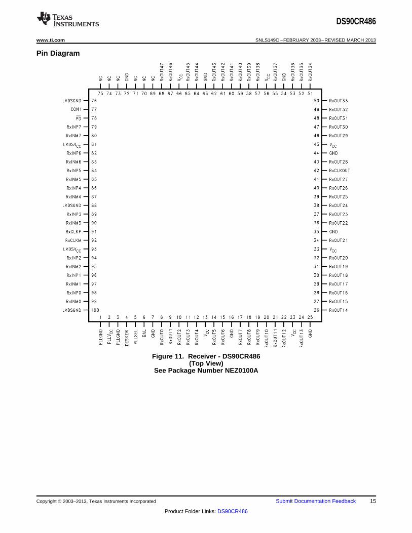
DS90CR486 PIN DESCRIPTIONS — CHANNEL LINK RECEIVER (1)
Pin Name I/O No. Description
RxINP I 8 Positive LVDS differential data inputs.
RxINM I 8 Negative LVDS differential data inputs.
RxOUT O 48 LVCMOS/LVTTL level data outputs. In PowerDown (PD = Low) mode, receiveroutputs are forced to a Low state.
RxCLKP I 1 Positive LVDS differential clock input.
RxCLKM I 1 Negative LVDS differential clock input.
RxCLKOUT O 1 LVCMOS/LVTTL level clock output. The rising edge acts as data strobe.
PLLSEL I 1 Control input for PLL range select. This pin must be tied to VCC. No connect ortied to GND is reserved for future use.
(1) These receivers have input fail-safe bias circuitry to ensure a stable receiver output for floating or terminated receiver inputs. Underthese conditions receiver inputs will be in a HIGH state. If a clock signal is present, outputs will all be HIGH; if the cable inter-connectsare disconnected which results in floating/terminated inputs, the outputs will remain in the last valid state. A floating/terminated clockinput will result in a LOW clock output.
Copyright © 2003–2013, Texas Instruments Incorporated Submit Documentation Feedback 9
Product Folder Links: DS90CR486
DS90CR486
SNLS149C –FEBRUARY 2003–REVISED MARCH 2013 www.ti.com
Pin Name I/O No. Description
PD I 1 Power Down pin. This pin must be tied to input level of 2.5V to Vcc for normaloperation. When de-asserted (low input) the receiver outputs are Low. Please referto the APPLICATIONS INFORMATION on the back for more information.
DESKEW I 1 This pin must be tied to logic High or Vcc for normal operation of Deskew function.De-asserting a pulse of duration greater than 4 clock cycles will restart the deskewinitialization. Do NOT tie this pin to LOW. Please refer to the APPLICATIONSINFORMATION on the back for more information.
BAL I 1 LVCMOS/LVTTL level input. This pin must be tied to logic High or Vcc to enableDC Balance function(Figure 9). When tied low or left open, the DC Balance functionis disabled(Figure 8). Please refer to the APPLICATIONS INFORMATION on theback for more infomation.
CON1 I 1 Control Pin. This pin must be tied to logic High or Vcc.
VCC I 6 Power supply pins for LVCMOS/LVTTL outputs and digital circuitry.
GND I 8 Ground pins for LVCMOS/LVTTL outputs and digital circuitry.
PLLVCC I 1 Power supply for PLL circuitry.
PLLGND I 2 Ground pin for PLL circuitry.
LVDSVCC I 2 Power supply pin for LVDS inputs.
LVDSGND I 3 Ground pins for LVDS inputs.
NC 6 No Connect. Make NO Connection to these pins - leave open.
10 Submit Documentation Feedback Copyright © 2003–2013, Texas Instruments Incorporated
Product Folder Links: DS90CR486
DS90CR486
www.ti.com SNLS149C –FEBRUARY 2003–REVISED MARCH 2013
APPLICATIONS INFORMATION
DC BALANCE
In addition to data information an additional bit is transmitted on every LVDS data signal line during each cycleas shown in Figure 9. This bit is the DC balance bit (DCB). The purpose of the DC Balance bit is to minimize theshort- and long-term DC bias on the signal lines. This is achieved by selectively sending the data eitherunmodified or inverted.
The value of the DC balance bit is calculated from the running word disparity and the data disparity of the currentword to be sent. The data disparity of the current word shall be calculated by subtracting the number of bits ofvalue 0 from the number of bits value 1 in the current word. Initially, the running word disparity may be any valuebetween +7 and −6. The running word disparity shall be calculated as a continuous sum of all the modified datadisparity values, where the unmodified data disparity value is the calculated data disparity minus 1 if the data issent unmodified and 1 plus the inverse of the calculated data disparity if the data is sent inverted. The value ofthe running word disparity shall saturate at +7 and −6.
The value of the DC balance bit (DCB) shall be 0 when the data is sent unmodified and 1 when the data is sentinverted. To determine whether to send data unmodified or inverted, the running word disparity and the currentdata disparity are used. If the running word disparity is positive and the current data disparity is positive, the datashall be sent inverted. If the running word disparity is positive and the current data disparity is zero or negative,the data shall be sent unmodified. If the running word disparity is negative and the current data disparity ispositive, the data shall be sent unmodified. If the running word disparity is negative and the current data disparityis zero or negative, the data shall be sent inverted. If the running word disparity is zero, the data shall be sentinverted.
DC Balance mode is set when the BAL pin on the transmitter and receiver are tied HIGH - see DS90CR486 PINDESCRIPTIONS — CHANNEL LINK RECEIVER.
DESKEW
The "DESKEW” function on this receiver will deskew or compensate fixed interconnect skew between datasignals, with respect to the rising edge of the LVDS clock, on each of the independent differential pairs (pair-to-pair skew). The deskew initialization or calibration is done automatically when the device is powered up. Thecontrol pin CON1 must set High and the Deskew pin must set to High on the DS90CR486. However, the Deskewcalibration can also be performed after the device is powered up. De-asserting with a pulse of duration greaterthan four clock cycles to the Deskew pin to restart the calibration of deskew. The calibration takes 4096 clockcycles to complete after the TX and RX PLLs lock (20ms). No RxIN data is sampled during this period. The dataoutputs during this period will be Low. For normal operation, deskew pin must set to High. Setting the deskew pinto Low or No Connect will continuously re-calibrate the sampling strobes. Data outputs are Low during thisperiod.
In order for the deskew function to work properly, it must be intialized. The DS90CR486 deskew can be initializedwith any data pattern with a minimum of 1 transition per clock cycle; however, having multiple transition per clockcycle will further improve the chance for the deskew circuit to find the optimal edge. Therefore, there are mulitipleways to initialize the deskew function depending on the setup configuration (Please refer to Figure 10). Forexample, to initialize the operation of deskew using DS90CR485 and DS90CR486 in DC balance mode, theDS_OPT pin at the input of the transmitter DS90CR485 can be set High OR Low when powered up. The periodof this input to the DS_OPT pin must be at least 20ms (TX and RX PLLs lock time) plus 4096 clock cycles inorder for the receiver to complete the deskew operation. For other configuration setup with DS90CR483 andDS90CR484, please refer to the flow chart on Figure 10.
The DS_OPT pin at the input of the transmitter (DS90CR485) can be used to initiate the deskew calibrationpattern. Depends on the configuration, it can be set High or applied Low when power up in order for the receiverto complete the deskew operation. For this reason, the LVDS clock signal with DS_OPT applied high (active datasampling) shall be 1111000 or 1110000 pattern and the LVDS data lines (TxOUT 0-7) shall be High for one clockcycle and Low for the next clock cycle. During the deskew operation with DS_OPT applied low, the LVDS clocksignal shall be 1111100 or 1100000 pattern. The transmitter will also output a series of 1111000 or 1110000 ontothe LVDS data lines (TxOUT 0-7) during deskew so that the receiver can automatically calibrated the datasampling strobes at the receiver inputs. Each data channel is deskewed independently and is tuned over aspecific range. Please refer to corresponding receiver datasheet for a list of deskew ranges.
Copyright © 2003–2013, Texas Instruments Incorporated Submit Documentation Feedback 11
Product Folder Links: DS90CR486
DS90CR486
SNLS149C –FEBRUARY 2003–REVISED MARCH 2013 www.ti.com
Note that the deskew initialization must be performed at least once after the PLL has locked to the input clockfrequency, and it must be done at the time when the receiver is powered up and PLL has locked. If power is lost,or if the cable has been swithcd or disconnected, the initialization procedure must be repeated or else thereceiver may not sample the incoming LVDS data correctly.
POWER DOWN
The receiver provides a power down feature. When de-asserted current draw through the supply pins isminimized and the PLLs are shut down. The receiver outputs are forced to an active LOW state when in thepower down mode. (See DS90CR486 Pin Descriptions — Channel Link Receiver Table). This is not aLVCMOS/LVTTL input pin and has a high input threshold. For normal operation, this pin must be tied to an inputlevel of 2.5V to Vcc.
CONFIGURATIONS
The chipset is designed to be connected typically to a single receiver load. This is known as a point-to-pointconfiguration. It is also possible to drive multiple receiver loads if certain restrictions are made(i.e. low data rate).Only the final receiver at the end of the interconnect should provide termination across the pair. In this case, thedriver still sees the intended DC load of 100 Ohms. Receivers connected to the cable between the transmitterand the final receiver must not load down the signal. To meet this system requirement, stub lengths from the lineto the receiver inputs must be kept very short.
CABLE TERMINATION
A termination resistor is required for proper operation to be obtained. The termination resistor should be equal tothe differential impedance of the media being driven. This should be in the range of 90 to 132 Ohms. 100 Ohmsis a typical value common used with standard 100 Ohm twisted pair cables. This resistor is required for control ofreflections and also to complete the current loop. It should be placed as close to the receiver inputs to minimizethe stub length from the resistor to the receiver input pins.
HOW TO CONFIGURE FOR BACKPLANE APPLICATIONS
In a backplane application with differential line impedance of 100Ω the differential line pair-to-pair skew cancontrolled by trace layout. The transmitter-DS90CR485 “DS_OPT” pin may be set high. In a backplaneapplication with short PCB distance traces, pre-emphasis from the transmitter is typically not required. The “PRE”pin should be left open (do not tie to ground). A resistor pad provision for a pull up resistor to Vcc can beimplemented in case pre-emphasis is needed to counteract heavy capacitive loading effects.
SUPPLY BYPASS RECOMMENDATIONS
Bypass capacitors must be used on the power supply pins. Different pins supply different portions of the circuit,therefore capacitors should be nearby all power supply pins except as noted in the DS90CR486 PinDescriptions — Channel Link Receiver table. Use high frequency ceramic (surface mount recommended) 0.1μFcapacitors close to each supply pin. If space allows, a 0.01μF capacitor should be used in parallel, with thesmallest value closest to the device pin. Additional scattered capacitors over the printed circuit board will improvedecoupling. Multiple (large) via should be used to connect the decoupling capacitors to the power plane. A 4.7 to10μF bulk cap is recommended near the PLLVCC pins and also the LVDSVCC pins. Connections between thecaps and the pin should use wide traces.
RECEIVER OUTPUT DRIVE STRENGTH
The DS90CR486 output specifies a 8pF load, VOH and VOL are tested at ± 2mA, which is intended for only 1 ormaybe 2 loads. The DS90CR486 receiver’s output driving capability has improved over prior generation ofChannel Link devices. Additional buffering at the receiver output is not necessary. If high fan-out is required orlong transmission line driving capability, buffering the receiver output is recommended. Receiver outputs do notsupport / provide a TRI-STATE function.
LVDS INTERCONNECT GUIDELINES
See AN-1108 (SNLA008) and AN-905 (SNLA035) for full details.• Use 100Ω coupled differential pairs• Use the S/2S/3S rule in spacings
12 Submit Documentation Feedback Copyright © 2003–2013, Texas Instruments Incorporated
Product Folder Links: DS90CR486
Select TX
Select RX Select RX
Balance
Mode
Balance
Mode
Balance
Mode
Balance
Mode
DESKEW
Not supportedConfiguration 6
DESKEW
Not supportedConfiguration 3Configuration 1 Configuration 4 Configuration 5Configuration 2
CR481/3 CR485O
N
OFFO
N
OFFO
N
OFF
CR484 CR
48
6
CR486
CR
48
4
ON
OFF
DS90CR486
www.ti.com SNLS149C –FEBRUARY 2003–REVISED MARCH 2013
– S = space between the pair– 2S = space between pairs– 3S = space to TTL signal
• Minimize the number of VIA• Use differential connectors when operating above 500Mbps line speed• Maintain balance of the traces• Minimize skew within the pair• Minimize skew between pairs• Terminate as close to the RXinputs as possible
For more information:
Channel Link Applications Notes currently available:• AN-1041 Introduction to Channel Link (literature number SNLA218)• AN-1108 PCB and Interconnect Guidelines (literature number SNLA008)• AN-905 Differential Impedance (literature number SNLA035)• TI’s LVDS Owner’s Manual (literature number SNLA187)
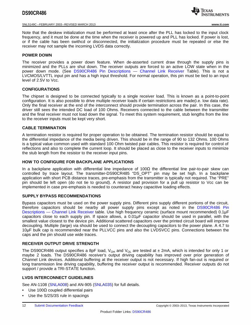
Figure 10. Deskew Configuration Setup Chart
CONFIGURATION 1
DS90CR481/483 and DS90CR484 with DC Balance ON (BAL=High, 33MHz to 80MHz) − The DS_OPT pin atthe input of the transmitter DS90CR481/483 must be applied low for a minimum of four clock cycles in order forthe receiver to complete the deskew operation. The input to the DS_OPT pin can be applied at any time after thePLL has locked to the input clock frequency. In this particular setup, the "DESKEW" pin on the receiverDS90CR484 must set High.
CONFIGURATION 2
DS90CR481/483 and DS90CR486 with DC Balance ON (BAL=High, CON1=High, 66MHz to 112MHz) − TheDS_OPT pin at the input of the transmitter DS90CR481/483 can be set to High OR Low when power up. Theperiod of this input to the DS_OPT pin must be at least 20ms (TX and RX PLLs lock time) plus 4096 clock cyclesin order for the receiver to complete the deskew operation. The "DESKEW" and CON1 pins on the receiverDS90CR486 must be tied to High for this setup.
Copyright © 2003–2013, Texas Instruments Incorporated Submit Documentation Feedback 13
Product Folder Links: DS90CR486
DS90CR486
SNLS149C –FEBRUARY 2003–REVISED MARCH 2013 www.ti.com
CONFIGURATION 3
DS90CR481/483 and DS90CR486 with DC Balance OFF (BAL=Low, CON1=High, 66MHz to 112MHz) − Theinput to the DS_OPT pin of the transmitter DS90CR481/483 in this configuration is completely ignored by thetransimitters. In order to initialize the deskew operation on the receiver DS90CR486, data and clcok must beapplied to the transimitter when power up. The "DESKEW" and CON1 pins on the receiver DS90CR486 must betied to High for this setup.
CONFIGURATION 4
DS90CR485 and DS90CR484 with DC Balance ON (BAL=High, 66MHz to 80MHz) − The DS_OPT pin at theinput of the transmitter DS90CR485 must be applied low for a minimum of four clock cycles in order for thereceiver to complete the deskew operation. The input to the DS_OPT pin can be applied at any time after thePLL has locked to the input clock frequency. In this setup, the "DESKEW" pin on the receiver DS90CR484 mustset High.
CONFIGURATION 5
DS90CR485 and DS90CR486 with DC Balance ON (BAL=Hiigh, CON1=High, 66MHz to 133MHz) − TheDS_OPT pin at the input of the transmitter DS90CR485 can be set to High OR Low when power up. The periodof this input to the DS_OPT pin must be at least 20ms (TX and RX PLLs lock time) plus 4096 clock cycles inorder for the receiver to complete the deskew operation. The "DESKEW" and CON1 pins on the receiverDS90CR486 must set High.
CONFIGURATION 6
DS90CR485 and DS90CR486 with DC Balance OFF (BAL=Low, CON1=High, 66MHz to 133MHz) −The input tothe DS_OPT pin of the transmitter DS90CR485 in this configuration is completely ignored. In order to initializethe deskew operation on the receiver DS90CR486, data and clcok must be applied to the transimitter whenpower up. The "DESKEW" and CON1 pins on the receiver DS90CR486 must set High.
DESKEW NOT SUPPORTED
Deskew function is NOT supported in these configuration setups. The deskew feature is only supported with DCBalance ON (BAL=High) for DS90CR484. Note that the deskew function in the DS90CR486 works in both DCBalance and NON-DC Balance modes.
NOTEFor more details on Deskew operation, please refer to the APPLICATIONSINFORMATION section.
14 Submit Documentation Feedback Copyright © 2003–2013, Texas Instruments Incorporated
Product Folder Links: DS90CR486
DS90CR486
www.ti.com SNLS149C –FEBRUARY 2003–REVISED MARCH 2013
Pin Diagram
Figure 11. Receiver - DS90CR486(Top View)
See Package Number NEZ0100A
Copyright © 2003–2013, Texas Instruments Incorporated Submit Documentation Feedback 15
Product Folder Links: DS90CR486
DS90CR486
SNLS149C –FEBRUARY 2003–REVISED MARCH 2013 www.ti.com
REVISION HISTORY
Changes from Revision B (March 2013) to Revision C Page
• Changed layout of National Data Sheet to TI format .......................................................................................................... 15
16 Submit Documentation Feedback Copyright © 2003–2013, Texas Instruments Incorporated
Product Folder Links: DS90CR486
PACKAGE OPTION ADDENDUM
www.ti.com 23-Jul-2015
Addendum-Page 1
PACKAGING INFORMATION
Orderable Device Status(1)
Package Type PackageDrawing
Pins PackageQty
Eco Plan(2)
Lead/Ball Finish(6)
MSL Peak Temp(3)
Op Temp (°C) Device Marking(4/5)
Samples
DS90CR486VS/NOPB ACTIVE TQFP NEZ 100 90 Green (RoHS& no Sb/Br)
CU NIPDAU Level-3-260C-168 HR -10 to 70 DS90CR486VS>B
DS90CR486VSX/NOPB ACTIVE TQFP NEZ 100 1000 Green (RoHS& no Sb/Br)
CU SN Level-3-260C-168 HR -10 to 70 DS90CR486VS>B
(1) The marketing status values are defined as follows:ACTIVE: Product device recommended for new designs.LIFEBUY: TI has announced that the device will be discontinued, and a lifetime-buy period is in effect.NRND: Not recommended for new designs. Device is in production to support existing customers, but TI does not recommend using this part in a new design.PREVIEW: Device has been announced but is not in production. Samples may or may not be available.OBSOLETE: TI has discontinued the production of the device.
(2) Eco Plan - The planned eco-friendly classification: Pb-Free (RoHS), Pb-Free (RoHS Exempt), or Green (RoHS & no Sb/Br) - please check http://www.ti.com/productcontent for the latest availabilityinformation and additional product content details.TBD: The Pb-Free/Green conversion plan has not been defined.Pb-Free (RoHS): TI's terms "Lead-Free" or "Pb-Free" mean semiconductor products that are compatible with the current RoHS requirements for all 6 substances, including the requirement thatlead not exceed 0.1% by weight in homogeneous materials. Where designed to be soldered at high temperatures, TI Pb-Free products are suitable for use in specified lead-free processes.Pb-Free (RoHS Exempt): This component has a RoHS exemption for either 1) lead-based flip-chip solder bumps used between the die and package, or 2) lead-based die adhesive used betweenthe die and leadframe. The component is otherwise considered Pb-Free (RoHS compatible) as defined above.Green (RoHS & no Sb/Br): TI defines "Green" to mean Pb-Free (RoHS compatible), and free of Bromine (Br) and Antimony (Sb) based flame retardants (Br or Sb do not exceed 0.1% by weightin homogeneous material)
(3) MSL, Peak Temp. - The Moisture Sensitivity Level rating according to the JEDEC industry standard classifications, and peak solder temperature.
(4) There may be additional marking, which relates to the logo, the lot trace code information, or the environmental category on the device.
(5) Multiple Device Markings will be inside parentheses. Only one Device Marking contained in parentheses and separated by a "~" will appear on a device. If a line is indented then it is a continuationof the previous line and the two combined represent the entire Device Marking for that device.
(6) Lead/Ball Finish - Orderable Devices may have multiple material finish options. Finish options are separated by a vertical ruled line. Lead/Ball Finish values may wrap to two lines if the finishvalue exceeds the maximum column width.
Important Information and Disclaimer:The information provided on this page represents TI's knowledge and belief as of the date that it is provided. TI bases its knowledge and belief on informationprovided by third parties, and makes no representation or warranty as to the accuracy of such information. Efforts are underway to better integrate information from third parties. TI has taken andcontinues to take reasonable steps to provide representative and accurate information but may not have conducted destructive testing or chemical analysis on incoming materials and chemicals.TI and TI suppliers consider certain information to be proprietary, and thus CAS numbers and other limited information may not be available for release.
PACKAGE OPTION ADDENDUM
www.ti.com 23-Jul-2015
Addendum-Page 2
In no event shall TI's liability arising out of such information exceed the total purchase price of the TI part(s) at issue in this document sold by TI to Customer on an annual basis.
TAPE AND REEL INFORMATION
*All dimensions are nominal
Device PackageType
PackageDrawing
Pins SPQ ReelDiameter
(mm)
ReelWidth
W1 (mm)
A0(mm)
B0(mm)
K0(mm)
P1(mm)
W(mm)
Pin1Quadrant
DS90CR486VSX/NOPB TQFP NEZ 100 1000 330.0 32.4 18.0 18.0 1.6 24.0 32.0 Q2
PACKAGE MATERIALS INFORMATION
www.ti.com 14-Feb-2015
Pack Materials-Page 1
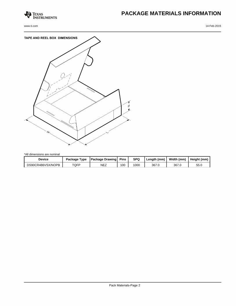
*All dimensions are nominal
Device Package Type Package Drawing Pins SPQ Length (mm) Width (mm) Height (mm)
DS90CR486VSX/NOPB TQFP NEZ 100 1000 367.0 367.0 55.0
PACKAGE MATERIALS INFORMATION
www.ti.com 14-Feb-2015
Pack Materials-Page 2
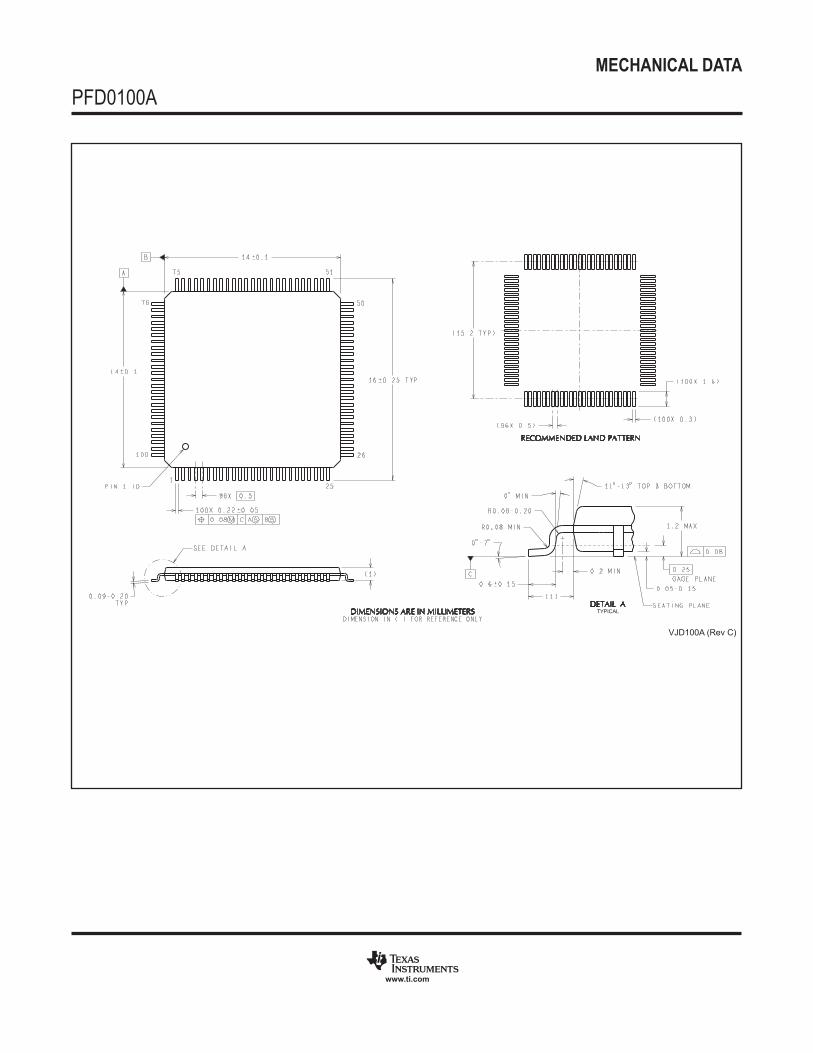
MECHANICAL DATA
PFD0100A
www.ti.com
VJD100A (Rev C)
TYPICAL
a0412025
Text Box
NEZ0100A
IMPORTANT NOTICE
Texas Instruments Incorporated and its subsidiaries (TI) reserve the right to make corrections, enhancements, improvements and otherchanges to its semiconductor products and services per JESD46, latest issue, and to discontinue any product or service per JESD48, latestissue. Buyers should obtain the latest relevant information before placing orders and should verify that such information is current andcomplete. All semiconductor products (also referred to herein as “components”) are sold subject to TI’s terms and conditions of salesupplied at the time of order acknowledgment.TI warrants performance of its components to the specifications applicable at the time of sale, in accordance with the warranty in TI’s termsand conditions of sale of semiconductor products. Testing and other quality control techniques are used to the extent TI deems necessaryto support this warranty. Except where mandated by applicable law, testing of all parameters of each component is not necessarilyperformed.TI assumes no liability for applications assistance or the design of Buyers’ products. Buyers are responsible for their products andapplications using TI components. To minimize the risks associated with Buyers’ products and applications, Buyers should provideadequate design and operating safeguards.TI does not warrant or represent that any license, either express or implied, is granted under any patent right, copyright, mask work right, orother intellectual property right relating to any combination, machine, or process in which TI components or services are used. Informationpublished by TI regarding third-party products or services does not constitute a license to use such products or services or a warranty orendorsement thereof. Use of such information may require a license from a third party under the patents or other intellectual property of thethird party, or a license from TI under the patents or other intellectual property of TI.Reproduction of significant portions of TI information in TI data books or data sheets is permissible only if reproduction is without alterationand is accompanied by all associated warranties, conditions, limitations, and notices. TI is not responsible or liable for such altereddocumentation. Information of third parties may be subject to additional restrictions.Resale of TI components or services with statements different from or beyond the parameters stated by TI for that component or servicevoids all express and any implied warranties for the associated TI component or service and is an unfair and deceptive business practice.TI is not responsible or liable for any such statements.Buyer acknowledges and agrees that it is solely responsible for compliance with all legal, regulatory and safety-related requirementsconcerning its products, and any use of TI components in its applications, notwithstanding any applications-related information or supportthat may be provided by TI. Buyer represents and agrees that it has all the necessary expertise to create and implement safeguards whichanticipate dangerous consequences of failures, monitor failures and their consequences, lessen the likelihood of failures that might causeharm and take appropriate remedial actions. Buyer will fully indemnify TI and its representatives against any damages arising out of the useof any TI components in safety-critical applications.In some cases, TI components may be promoted specifically to facilitate safety-related applications. With such components, TI’s goal is tohelp enable customers to design and create their own end-product solutions that meet applicable functional safety standards andrequirements. Nonetheless, such components are subject to these terms.No TI components are authorized for use in FDA Class III (or similar life-critical medical equipment) unless authorized officers of the partieshave executed a special agreement specifically governing such use.Only those TI components which TI has specifically designated as military grade or “enhanced plastic” are designed and intended for use inmilitary/aerospace applications or environments. Buyer acknowledges and agrees that any military or aerospace use of TI componentswhich have not been so designated is solely at the Buyer's risk, and that Buyer is solely responsible for compliance with all legal andregulatory requirements in connection with such use.TI has specifically designated certain components as meeting ISO/TS16949 requirements, mainly for automotive use. In any case of use ofnon-designated products, TI will not be responsible for any failure to meet ISO/TS16949.
Products ApplicationsAudio www.ti.com/audio Automotive and Transportation www.ti.com/automotiveAmplifiers amplifier.ti.com Communications and Telecom www.ti.com/communicationsData Converters dataconverter.ti.com Computers and Peripherals www.ti.com/computersDLP® Products www.dlp.com Consumer Electronics www.ti.com/consumer-appsDSP dsp.ti.com Energy and Lighting www.ti.com/energyClocks and Timers www.ti.com/clocks Industrial www.ti.com/industrialInterface interface.ti.com Medical www.ti.com/medicalLogic logic.ti.com Security www.ti.com/securityPower Mgmt power.ti.com Space, Avionics and Defense www.ti.com/space-avionics-defenseMicrocontrollers microcontroller.ti.com Video and Imaging www.ti.com/videoRFID www.ti-rfid.comOMAP Applications Processors www.ti.com/omap TI E2E Community e2e.ti.comWireless Connectivity www.ti.com/wirelessconnectivity
Mailing Address: Texas Instruments, Post Office Box 655303, Dallas, Texas 75265Copyright © 2016, Texas Instruments Incorporated