DS90UH926Q 720p 24-bit Color FPD-Link III Deserializer with ...
58
R[7:0] HS VS PCLK PDB Serializer Deserializer DE RGB Display 720p 24-bit color depth RGB Digital Display Interface HOST Graphics Processor FPD-Link III 1 Pair / AC Coupled DS90UH925Q-Q1 DS90UH926Q-Q1 100 ohm STP Cable PASS V DDIO OSS_SEL SCL SDA INTB I2S AUDIO (STEREO) OEN LOCK IDx DAP DAP 0.1 2F 0.1 2F G[7:0] B[7:0] SCL SDA IDx R[7:0] HS VS PCLK DE G[7:0] B[7:0] RIN+ RIN- DOUT+ DOUT- (1.8V or 3.3V) (1.8V or 3.3V) (3.3V) (3.3V) V DDIO 3 / I2S AUDIO (STEREO) 3 / MODE_SEL MODE_SEL MCLK PDB INTB_IN V DD33 VDD33 Product Folder Sample & Buy Technical Documents Tools & Software Support & Community Reference Design DS90UH926Q-Q1 SNLS337K – OCTOBER 2010 – REVISED JANUARY 2015 DS90UH926Q-Q1 720p 24-Bit Color FPD-Link III Deserializer With HDCP 1 Features 3 Description The DS90UH926Q-Q1 deserializer, in conjunction 1• Integrated HDCP Cipher Engine with On-Chip Key with the DS90UH925Q-Q1 serializer, provides a Storage solution for secure distribution of content-protected • Bidirectional Control Interface Channel Interface digital video within automotive entertainment with I 2 C Compatible Serial Control Bus systems. This chipset translates a parallel RGB video interface into a single-pair high-speed serialized • Supports High-Definition (720p) Digital Video interface. The digital video data is protected using the Format industry standard HDCP copy protection scheme. • RGB888 + VS, HS, DE and I2S Audio Supported The serial bus scheme, FPD-Link III, supports full • 5- to 85-MHz PCLK Supported duplex of high-speed forward data transmission and • Single 3.3-V Operation With 1.8-V or 3.3-V low-speed backchannel communication over a single differential link. Consolidation of video data and Compatible LVCMOS I/O Interface control over a single differential pair reduces the • AC-Coupled STP Interconnect up to 10 Meters interconnect size and weight, while also eliminating • Parallel LVCMOS Video Outputs skew issues and simplifying system design. • DC-Balanced and Scrambled Data With The DS90UH926Q-Q1 deserializer has a 31-bit Embedded Clock parallel LVCMOS output interface to accommodate • Adaptive Cable Equalization the RGB, video control, and audio data. The device extracts the clock from a high-speed serial stream. • Supports HDCP Repeater Application An output LOCK pin provides the link status if the • Image Enhancement (White Balance and incoming data stream is locked, without the use of a Dithering) and Internal Pattern Generation training sequence or special SYNC patterns, as well • EMI Minimization (SSCG and EPTO) as a reference clock. • Low Power Modes Minimize Power Dissipation An adaptive equalizer optimizes the maximum cable • Automotive-Grade Product: AEC-Q100 Grade 2 reach. EMI is minimized by output SSC generation Qualified (SSCG) and enhanced progressive turnon (EPTO) features. • Greater Than 8 kV HBM and ISO 10605 ESD Rating The HDCP cipher engine is implemented in both the serializer and deserializer. HDCP keys are stored in • Backward-Compatible Modes on-chip memory. 2 Applications Device Information (1) • Automotive Display for Navigation PART NUMBER PACKAGE BODY SIZE (NOM) • Rear Seat Entertainment Systems DS90UH926Q-Q1 WQFN (60) 9.00 mm × 9.00 mm (1) For all available packages, see the orderable addendum at the end of the data sheet. Application Diagram 1 An IMPORTANT NOTICE at the end of this data sheet addresses availability, warranty, changes, use in safety-critical applications, intellectual property matters and other important disclaimers. PRODUCTION DATA.
Transcript of DS90UH926Q 720p 24-bit Color FPD-Link III Deserializer with ...

R[7:0]
HSVS
PCLK
PDBSerializer Deserializer
DE
RGB Display720p
24-bit color depth
RG
B D
igita
l Dis
play
Inte
rfac
e
HOSTGraphicsProcessor
FPD-Link III1 Pair / AC Coupled
DS90UH925Q-Q1 DS90UH926Q-Q1100 ohm STP Cable
PASS
VDDIO
OSS_SEL
SCLSDA
INTB
I2S AUDIO (STEREO)
OEN
LOCK
IDx DAP DAP
0.1 PF 0.1 PFG[7:0]B[7:0]
SCLSDAIDx
R[7:0]
HSVS
PCLKDE
G[7:0]B[7:0]
RIN+
RIN-
DOUT+
DOUT-
(1.8V or 3.3V)(1.8V or 3.3V) (3.3V) (3.3V)VDDIO
3/
I2S AUDIO (STEREO)
3/MODE_SEL MODE_SEL
MCLK
PDB
INTB_IN
VDD33 VDD33
Product
Folder
Sample &Buy
Technical
Documents
Tools &
Software
Support &Community
ReferenceDesign
DS90UH926Q-Q1SNLS337K –OCTOBER 2010–REVISED JANUARY 2015
DS90UH926Q-Q1 720p 24-Bit Color FPD-Link III Deserializer With HDCP1 Features 3 Description
The DS90UH926Q-Q1 deserializer, in conjunction1• Integrated HDCP Cipher Engine with On-Chip Key
with the DS90UH925Q-Q1 serializer, provides aStoragesolution for secure distribution of content-protected
• Bidirectional Control Interface Channel Interface digital video within automotive entertainmentwith I2C Compatible Serial Control Bus systems. This chipset translates a parallel RGB video
interface into a single-pair high-speed serialized• Supports High-Definition (720p) Digital Videointerface. The digital video data is protected using theFormatindustry standard HDCP copy protection scheme.• RGB888 + VS, HS, DE and I2S Audio Supported The serial bus scheme, FPD-Link III, supports full
• 5- to 85-MHz PCLK Supported duplex of high-speed forward data transmission and• Single 3.3-V Operation With 1.8-V or 3.3-V low-speed backchannel communication over a single
differential link. Consolidation of video data andCompatible LVCMOS I/O Interfacecontrol over a single differential pair reduces the• AC-Coupled STP Interconnect up to 10 Metersinterconnect size and weight, while also eliminating
• Parallel LVCMOS Video Outputs skew issues and simplifying system design.• DC-Balanced and Scrambled Data With The DS90UH926Q-Q1 deserializer has a 31-bitEmbedded Clock parallel LVCMOS output interface to accommodate• Adaptive Cable Equalization the RGB, video control, and audio data. The device
extracts the clock from a high-speed serial stream.• Supports HDCP Repeater ApplicationAn output LOCK pin provides the link status if the• Image Enhancement (White Balance andincoming data stream is locked, without the use of aDithering) and Internal Pattern Generation training sequence or special SYNC patterns, as well
• EMI Minimization (SSCG and EPTO) as a reference clock.• Low Power Modes Minimize Power Dissipation An adaptive equalizer optimizes the maximum cable• Automotive-Grade Product: AEC-Q100 Grade 2 reach. EMI is minimized by output SSC generation
Qualified (SSCG) and enhanced progressive turnon (EPTO)features.• Greater Than 8 kV HBM and ISO 10605 ESD
Rating The HDCP cipher engine is implemented in both theserializer and deserializer. HDCP keys are stored in• Backward-Compatible Modeson-chip memory.
2 ApplicationsDevice Information(1)
• Automotive Display for Navigation PART NUMBER PACKAGE BODY SIZE (NOM)• Rear Seat Entertainment Systems DS90UH926Q-Q1 WQFN (60) 9.00 mm × 9.00 mm
(1) For all available packages, see the orderable addendum atthe end of the data sheet.
Application Diagram
1
An IMPORTANT NOTICE at the end of this data sheet addresses availability, warranty, changes, use in safety-critical applications,intellectual property matters and other important disclaimers. PRODUCTION DATA.

DS90UH926Q-Q1SNLS337K –OCTOBER 2010–REVISED JANUARY 2015 www.ti.com
Table of Contents7.2 Functional Block Diagram ....................................... 151 Features .................................................................. 17.3 Feature Description................................................. 152 Applications ........................................................... 17.4 Device Functional Modes........................................ 273 Description ............................................................. 17.5 Programming........................................................... 314 Revision History..................................................... 27.6 Register Maps ......................................................... 325 Pin Configuration and Functions ......................... 3
8 Application and Implementation ........................ 466 Specifications......................................................... 68.1 Application Information............................................ 466.1 Absolute Maximum Ratings ..................................... 68.2 Typical Application .................................................. 466.2 ESD Ratings.............................................................. 6
9 Power Supply Recommendations ...................... 496.3 Recommended Operating Conditions....................... 610 Layout................................................................... 496.4 Thermal Information .................................................. 7
10.1 Layout Guidelines ................................................. 496.5 DC Electrical Characteristics .................................... 710.2 Layout Example .................................................... 516.6 AC Electrical Characteristics..................................... 9
11 Device and Documentation Support ................. 526.7 DC and AC Serial Control Bus Characteristics......... 911.1 Documentation Support ........................................ 526.8 Recommended Timing Requirements for the Serial
Control Bus .............................................................. 10 11.2 Trademarks ........................................................... 526.9 Switching Characteristics ........................................ 10 11.3 Electrostatic Discharge Caution............................ 526.10 Typical Characteristics .......................................... 14 11.4 Glossary ................................................................ 52
7 Detailed Description ............................................ 15 12 Mechanical, Packaging, and OrderableInformation ........................................................... 527.1 Overview ................................................................. 15
4 Revision HistoryNOTE: Page numbers for previous revisions may differ from page numbers in the current version.
Changes from Revision J (April 2013) to Revision K Page
• Added Pin Configuration and Functions section, ESD Ratings table, Feature Description section, Device FunctionalModes, Application and Implementation section, Power Supply Recommendations section, Layout section, Deviceand Documentation Support section, and Mechanical, Packaging, and Orderable Information section .............................. 1
Changes from Revision I (August 2012) to Revision J Page
• Changed layout of National Data Sheet to TI format ............................................................................................................. 1
Changes from Revision H (March 2012) to Revision I Page
• Corrected Table 9: Configuration Select (MODE_SEL) #6 I2S Channel B (18–bit Mode) from L to H, corrected typoin table “DC and AC Serial Control Bus Characteristics” from VDDIO to VDD33, added Recommended FRC settingstable, added “When backward compatible mode = ON, set LFMODE = 0” under Functional Description. ReformattedTable 9 and added clarification to notes. Added clarification to notes on Table 11 Serial Control Bus Registers,address 0x02[3:0] (backwards compatible and LFMODE registers), added “Note: Do not enable SSCG feature ifPCLK source into the SER has an SSC clock already.” under Functional Description, EMI REDUCTIONFEATURES, Spread Spectrum Clock Generation (SSCG).................................................................................................... 1
Changes from Revision G (February 2012) to Revision H Page
• Deleted “DC Electrical Characteristics” PDB VDDIO = 1.71 to 1.89V, added under “SUPPLY CURRENT IDDZ, DDIOZ,IDDIOZMax = 10mA, added under “CML MONITOR DRIVER OUTPUT AC SPECIFICATIONS” EW Min = 0.3 UI ANDEH Min = 200 mV, added “INTERRUPT PIN — FUNCTIONAL DESCRIPTION AND USAGE (INTB)” underFunctional Description section, updated "POWER DOWN (PDB) description under Functional Description fromVDDIO to VDDIO = 3.0 to 3.6V or VDD33, updated Figure 24. Typical Connection Diagram ................................................. 1
2 Submit Documentation Feedback Copyright © 2010–2015, Texas Instruments Incorporated
Product Folder Links: DS90UH926Q-Q1

50
51
52
53
54
55
56
57
58
59
60
1 2 3 4 5 6 7 8 9 10 11 12
27
26
25
24
23
22
21
20
19
18
17
16
45 44 43 42 41 40 39 38 37 36 35 34
DS90UH926Q-Q1TOP VIEW
DAP = GND
I2S_WC/GPO_REG7
PDB
CAPP12
IDx
CMLOUTN
CMLOUTP
RIN-
RIN+
BISTC/INTB_IN
B2
B0/GPO_REG4
G7
G4
VDDIO
G2
G1/GPIO3
CMF
NC
CAPR12
CAPI2S B1/I2S_DB/GPO_REG5
G6
G5
G3
I2S
_CLK
/GP
O_R
EG
8
SC
L
B6
B4
SD
AB
IST
EN
RE
S1
PA
SS
R0/
GP
IO0
R1/
GP
IO1
R2
VD
DIO
R3
R4
R5
I2S
_DA
/GP
O_R
EG
6
VS
HS
B5
R6
B7
CA
PL1
2
PC
LK DE
VD
DIO
MO
DE
_SE
L
B3
33 32 31
R7
LOC
K
OE
N
30
29
28
VDD33_B
MCLK
G0/GPIO2
46
47
48
RES0
OSS_SEL
VDD33_A
13 14 15
49
DS90UH926Q-Q1www.ti.com SNLS337K –OCTOBER 2010–REVISED JANUARY 2015
5 Pin Configuration and Functions
NKB Package60-Pin WQFN With Exposed Thermal Pad
Top View
Pin FunctionsPIN
I/O, TYPE DESCRIPTIONNAME NO.
LVCMOS PARALLEL INTERFACER[7:0] 33, 34, 35, 36, O, LVCMOS RED Parallel Interface Data Output Pins
37, 39, 40, 41 with pulldown Leave open if unusedR0 can optionally be used as GPIO0 and R1 can optionally be used as GPIO1
G[7:0] 20, 21, 22, 23, O, LVCMOS GREEN Parallel Interface Data Output Pins25, 26, 27, 28 with pulldown Leave open if unused
G0 can optionally be used as GPIO2 and G1 can optionally be used as GPIO3.B[7:0] 9, 10, 11, 12, O, LVCMOS BLUE Parallel Interface Data Output Pins
14, 17, 18, 19 with pulldown Leave open if unusedB0 can optionally be used as GPO_REG4 and B1 can optionally be used as I2S_DB orGPO_REG5.
Copyright © 2010–2015, Texas Instruments Incorporated Submit Documentation Feedback 3
Product Folder Links: DS90UH926Q-Q1
DS90UH926Q-Q1SNLS337K –OCTOBER 2010–REVISED JANUARY 2015 www.ti.com
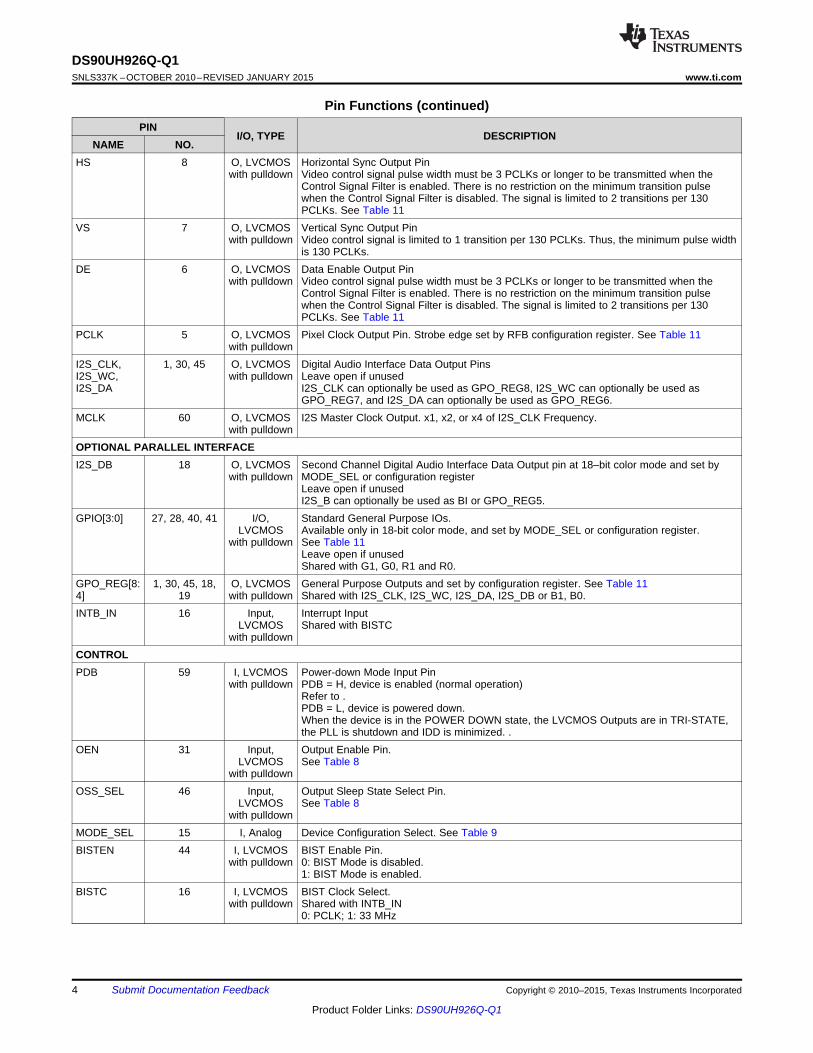
Pin Functions (continued)PIN
I/O, TYPE DESCRIPTIONNAME NO.
HS 8 O, LVCMOS Horizontal Sync Output Pinwith pulldown Video control signal pulse width must be 3 PCLKs or longer to be transmitted when the
Control Signal Filter is enabled. There is no restriction on the minimum transition pulsewhen the Control Signal Filter is disabled. The signal is limited to 2 transitions per 130PCLKs. See Table 11
VS 7 O, LVCMOS Vertical Sync Output Pinwith pulldown Video control signal is limited to 1 transition per 130 PCLKs. Thus, the minimum pulse width
is 130 PCLKs.DE 6 O, LVCMOS Data Enable Output Pin
with pulldown Video control signal pulse width must be 3 PCLKs or longer to be transmitted when theControl Signal Filter is enabled. There is no restriction on the minimum transition pulsewhen the Control Signal Filter is disabled. The signal is limited to 2 transitions per 130PCLKs. See Table 11
PCLK 5 O, LVCMOS Pixel Clock Output Pin. Strobe edge set by RFB configuration register. See Table 11with pulldown
I2S_CLK, 1, 30, 45 O, LVCMOS Digital Audio Interface Data Output PinsI2S_WC, with pulldown Leave open if unusedI2S_DA I2S_CLK can optionally be used as GPO_REG8, I2S_WC can optionally be used as
GPO_REG7, and I2S_DA can optionally be used as GPO_REG6.MCLK 60 O, LVCMOS I2S Master Clock Output. x1, x2, or x4 of I2S_CLK Frequency.
with pulldownOPTIONAL PARALLEL INTERFACEI2S_DB 18 O, LVCMOS Second Channel Digital Audio Interface Data Output pin at 18–bit color mode and set by
with pulldown MODE_SEL or configuration registerLeave open if unusedI2S_B can optionally be used as BI or GPO_REG5.
GPIO[3:0] 27, 28, 40, 41 I/O, Standard General Purpose IOs.LVCMOS Available only in 18-bit color mode, and set by MODE_SEL or configuration register.
with pulldown See Table 11Leave open if unusedShared with G1, G0, R1 and R0.
GPO_REG[8: 1, 30, 45, 18, O, LVCMOS General Purpose Outputs and set by configuration register. See Table 114] 19 with pulldown Shared with I2S_CLK, I2S_WC, I2S_DA, I2S_DB or B1, B0.INTB_IN 16 Input, Interrupt Input
LVCMOS Shared with BISTCwith pulldown
CONTROLPDB 59 I, LVCMOS Power-down Mode Input Pin
with pulldown PDB = H, device is enabled (normal operation)Refer to .PDB = L, device is powered down.When the device is in the POWER DOWN state, the LVCMOS Outputs are in TRI-STATE,the PLL is shutdown and IDD is minimized. .
OEN 31 Input, Output Enable Pin.LVCMOS See Table 8
with pulldownOSS_SEL 46 Input, Output Sleep State Select Pin.
LVCMOS See Table 8with pulldown
MODE_SEL 15 I, Analog Device Configuration Select. See Table 9BISTEN 44 I, LVCMOS BIST Enable Pin.
with pulldown 0: BIST Mode is disabled.1: BIST Mode is enabled.
BISTC 16 I, LVCMOS BIST Clock Select.with pulldown Shared with INTB_IN
0: PCLK; 1: 33 MHz
4 Submit Documentation Feedback Copyright © 2010–2015, Texas Instruments Incorporated
Product Folder Links: DS90UH926Q-Q1

DS90UH926Q-Q1www.ti.com SNLS337K –OCTOBER 2010–REVISED JANUARY 2015
Pin Functions (continued)PIN
I/O, TYPE DESCRIPTIONNAME NO.
I2CIDx 56 I, Analog I2C Serial Control Bus Device ID Address Select
External pull-up to VDD33 is required under all conditions, DO NOT FLOAT.Connect to external pullup and pulldown resistor to create a voltage divider.See Figure 23
SCL 3 I/O, I2C Clock Input / Output InterfaceLVCMOS Must have an external pullup to VDD33, DO NOT FLOAT.
Open-Drain Recommended pullup: 4.7kΩ.SDA 2 I/O, I2C Data Input / Output Interface
LVCMOS Must have an external pullup to VDD33, DO NOT FLOAT.Open-Drain Recommended pullup: 4.7 kΩ.
STATUSLOCK 32 O, LVCMOS LOCK Status Output Pin
with pulldown 0: PLL is unlocked, RGB[7:0], I2S[2:0], HS, VS, DE and PCLK output states are controlledby OEN. May be used as Link Status or Display Enable1: PLL is Locked, outputs are active
PASS 42 O, LVCMOS PASS Output Pinwith pulldown 0: One or more errors were detected in the received payload
1: ERROR FREE TransmissionLeave Open if unused. Route to test point (pad) recommended
FPD-LINK III SERIAL INTERFACERIN+ 49 I, LVDS True Input.
The interconnection should be AC-coupled to this pin with a 0.1-μF capacitor.RIN- 50 I, LVDS Inverting Input.
The interconnection should be AC-coupled to this pin with a 0.1-μF capacitor.CMLOUTP 52 O, LVDS True CML Output
Monitor point for equalized differential signalCMLOUTN 53 O, LVDS Inverting CML Output
Monitor point for equalized differential signalCMF 51 Analog Common Mode Filter. Connect 0.1-μF capacitor to GNDPOWER (1) AND GROUNDVDD33_A, 48, 29 Power Power to on-chip regulator 3.0 V – 3.6 V. Requires 4.7 uF to GND at each VDD pin.VDD33_BVDDIO 13, 24, 38 Power LVCMOS I/O Power 1.8 V ±5% OR 3.0 V – 3.6 V. Requires 4.7 uF to GND at each VDDIO
pin.GND DAP Ground DAP is the large metal contact at the bottom side, located at the center of the WQFN
package. Connect to the ground plane (GND) with at least 9 vias.REGULATOR CAPACITORCAPR12 55 CAP Decoupling capacitor connection for on-chip regulator. Requires a 4.7uF to GND at each
CAP pin.CAPP12 57CAPI2S 58CAPL12 4 CAP Decoupling capacitor connection for on-chip regulator. Requires two 4.7uF to GND at this
CAP pin.OTHERSNC 54 NC No connect. This pin may be left open or tied to any level.RES[1:0] 43.47 GND Reserved. Tie to Ground.
(1) The VDD (VDD33 and VDDIO) supply ramp should be faster than 1.5 ms with a monotonic rise.
Copyright © 2010–2015, Texas Instruments Incorporated Submit Documentation Feedback 5
Product Folder Links: DS90UH926Q-Q1

DS90UH926Q-Q1SNLS337K –OCTOBER 2010–REVISED JANUARY 2015 www.ti.com
6 Specifications
6.1 Absolute Maximum RatingsSee (1) (2) (3).
MIN MAX UNITSupply Voltage – VDD33 −0.3 4.0 VSupply Voltage – VDDIO −0.3 4.0 VLVCMOS I/O Voltage −0.3 (VDDIO + 0.3) VDeserializer Input Voltage −0.3 2.75 VJunction Temperature 150 °C60 WQFN Package Derate above 25°C 1/ θJA °C/WMaximum Power RθJA 31 °C/WDissipation Capacity at
RθJC 2.4 °C/W25°CStorage temperature, Tstg −65 150 °C
(1) Stresses beyond those listed under Absolute Maximum Ratings may cause permanent damage to the device. These are stress ratingsonly, which do not imply functional operation of the device at these or any other conditions beyond those indicated under RecommendedOperating Conditions. Exposure to absolute-maximum-rated conditions for extended periods may affect device reliability.
(2) If Military/Aerospace specified devices are required, please contact the Texas Instruments Sales Office/ Distributors for availability andspecifications.
(3) For soldering specifications, see product folder at www.ti.com and SNOA549.
6.2 ESD RatingsVALUE UNIT
Human-body model (HBM), per AEC Q100-002 (1) ±8000Charged-device model (CDM), per AEC Q100-011 ±1250Machine model, all pins ±250
Air Discharge (Pin 49 and 50) ±15000(IEC, powered-up only)Electrostatic RD = 330 Ω, CS = 150 pFV(ESD) Contact Discharge (Pin 49 and 50) ±8000 Vdischarge
Air Discharge (Pin 49 and 50) ±15000(ISO10605)RD = 330 Ω, CS = 150 pF Contact Discharge (Pin 49 and 50) ±8000
Air Discharge (Pin 49 and 50) ±15000(ISO10605)RD = 2 kΩ, CS = 150 & 330 pF Contact Discharge (Pin 49 and 50) ±8000
(1) AEC Q100-002 indicates that HBM stressing shall be in accordance with the ANSI/ESDA/JEDEC JS-001 specification.
6.3 Recommended Operating ConditionsMIN NOM MAX UNIT
Supply Voltage (VDD33) 3 3.3 3.6 VLVCMOS Supply Voltage (VDDIO) Connect VDDIO to 3.3 V and use 3.3-V IOs 3 3.3 3.6 V
Connect VDDIO to 1.8 V and use 1.8-V IOs 1.71 1.8 1.89 VOperating Free Air Temperature (TA) −40 25 105 °CPCLK Frequency 5 85 MHzSupply Noise (1) 100 mVP-P
(1) Supply noise testing was done with minimum capacitors on the PCB. A sinusoidal signal is AC coupled to the VDD33 and VDDIOsupplieswith amplitude = 100 mVp-p measured at the device VDD33 and VDDIO pins. Bit error rate testing of input to the Ser and output of theDes with 10-meter cable shows no error when the noise frequency on the Ser is less than 50 MHz. The Des on the other hand showsno error when the noise frequency is less than 50 MHz.
6 Submit Documentation Feedback Copyright © 2010–2015, Texas Instruments Incorporated
Product Folder Links: DS90UH926Q-Q1

DS90UH926Q-Q1www.ti.com SNLS337K –OCTOBER 2010–REVISED JANUARY 2015
6.4 Thermal InformationDS90UH926Q-Q1
THERMAL METRIC (1) NKB (WQFN) UNIT60 PINS
RθJA Junction-to-ambient thermal resistance 26.2RθJC(top) Junction-to-case (top) thermal resistance 8.1RθJB Junction-to-board thermal resistance 5.2
°C/WψJT Junction-to-top characterization parameter 0.1ψJB Junction-to-board characterization parameter 5.2RθJC(bot) Junction-to-case (bottom) thermal resistance 1.1
(1) For more information about traditional and new thermal metrics, see the IC Package Thermal Metrics application report, SPRA953.
6.5 DC Electrical CharacteristicsOver recommended operating supply and temperature ranges unless otherwise specified. (1) (2) (3)
PARAMETER TEST CONDITIONS PIN/FREQ. MIN TYP MAX UNITLVCMOS I/O DC SPECIFICATIONS
High Level InputVIH VDDIO = 3.0 to 3.6 V 2.0 VDDIO VVoltageLow Level Input PDBVIL VDDIO = 3.0 to 3.6 V GND 0.8 VVoltage
IIN Input Current VIN = 0 V or VDDIO = 3.0 to 3.6 V −10 ±1 +10 μAVDDIO = 3.0 to 3.6 V 2.0 VDDIO V
High Level InputVIH 0.65 ×Voltage VDDIO = 1.71 to 1.89 V VDDIO VVDDIO
VDDIO = 3.0 to 3.6 V GND 0.8 VLow Level Input OEN, OSS_SEL,VIL 0.35*Voltage BISTEN, BISTC /VDDIO = 1.71 to 1.89 V GND VVDDIOINTB_IN, GPIO[3:0]
VDDIO = 3.0 −10 ±1 +10 μAto 3.6 VIIN Input Current VIN = 0 V or VDDIO VDDIO = 1.7 −10 ±1 +10 μAto 1.89 V
VDDIO = 3.0 to 2.4 VDDIO V3.6 VHigh Level OutputVOH IOH = −4mAVoltage VDDIO = 1.7 VDDIO- VDDIO Vto 1.89 V 0.45R[7:0], G[7:0], B[7:0],HS, VS, DE, PCLK,VDDIO = 3.0 to GND 0.4 VLOCK, PASS, MCLK,3.6 VLow Level OutputVOL IOL = +4mA I2S_CLK, I2S_WC,Voltage VDDIO = 1.7 I2S_DA, I2S_DB, GND 0.35 Vto 1.89 V GPO_REG[8:4]
Output Short CircuitIOS VOUT = 0 V −60 mACurrentIOZ Tri-state Output Current VOUT = 0 V or VDDIO, PDB = L −10 +10 μA
(1) The Electrical Characteristics tables list ensured specifications under the listed Recommended Operating Conditions except asotherwise modified or specified by the Electrical Characteristics Conditions and/or Notes. Typical specifications are estimations only andare not ensured.
(2) Typical values represent most likely parametric norms at VDD = 3.3 V, TA = 25°C, and at the Recommended Operation Conditions at thetime of product characterization and are not ensured.
(3) Current into device pins is defined as positive. Current out of a device pin is defined as negative. Voltages are referenced to groundexcept VOD and ΔVOD, which are differential voltages.
Copyright © 2010–2015, Texas Instruments Incorporated Submit Documentation Feedback 7
Product Folder Links: DS90UH926Q-Q1

DS90UH926Q-Q1SNLS337K –OCTOBER 2010–REVISED JANUARY 2015 www.ti.com
DC Electrical Characteristics (continued)Over recommended operating supply and temperature ranges unless otherwise specified.(1) (2) (3)
PARAMETER TEST CONDITIONS PIN/FREQ. MIN TYP MAX UNITFPD-LINK III CML RECEIVER INPUT DC SPECIFICATIONS
Differential ThresholdVTH +50 mVHigh Voltage VCM = 2.5 V(Internal VBIAS)Differential ThresholdVTL −50 mVLow Voltage
RIN+, RIN-Differential Common-VCM 1.8 Vmode VoltageInternal TerminationRT 80 100 120 ΩResistor - Differential
CML MONITOR DRIVER OUTPUT DC SPECIFICATIONSDifferential Output CMLOUTP,VODp-p RL = 100Ω 360 mVp-pVoltage CMLOUTN
SUPPLY CURRENTIDD1 VDD33= 3.6 V VDD33 125 145 mASupply Current CL = 12pF,
(includes load current) Checker Board Pattern VDDIO= 3.6 V 110 118 mAIDDIO1 VDDIOf = 85MHz Figure 1 VDDIO = 1.89 V 60 75 mAIDD2 VDD33 = 3.6 V VDD33 125 145 mASupply Current CL = 4pF
(includes load current) Checker Board Pattern, VDDIO = 3.6 V 75 85 mAIDDIO2 VDDIOf = 85MHz Figure 1 VDDIO = 1.89 V 50 65 mAIDDS VDD33 = 3.6 V VDD33 90 115 mA
Supply Current Sleep Without Input Serial VDDIO = 3.6 V 3 5 mAMode StreamIDDIOS VDDIOVDDIO = 1.89 V 2 3 mAIDDZ VDD33 = 3.6 V VDD33 2 10 mAPDB = L, All LVCMOSSupply Current Power inputs are floating or tied VDDIO = 3.6 V 0.05 10 mADownIDDIOZ VDDIOto GND VDDIO = 1.89 V 0.05 10 mA
8 Submit Documentation Feedback Copyright © 2010–2015, Texas Instruments Incorporated
Product Folder Links: DS90UH926Q-Q1
DS90UH926Q-Q1www.ti.com SNLS337K –OCTOBER 2010–REVISED JANUARY 2015
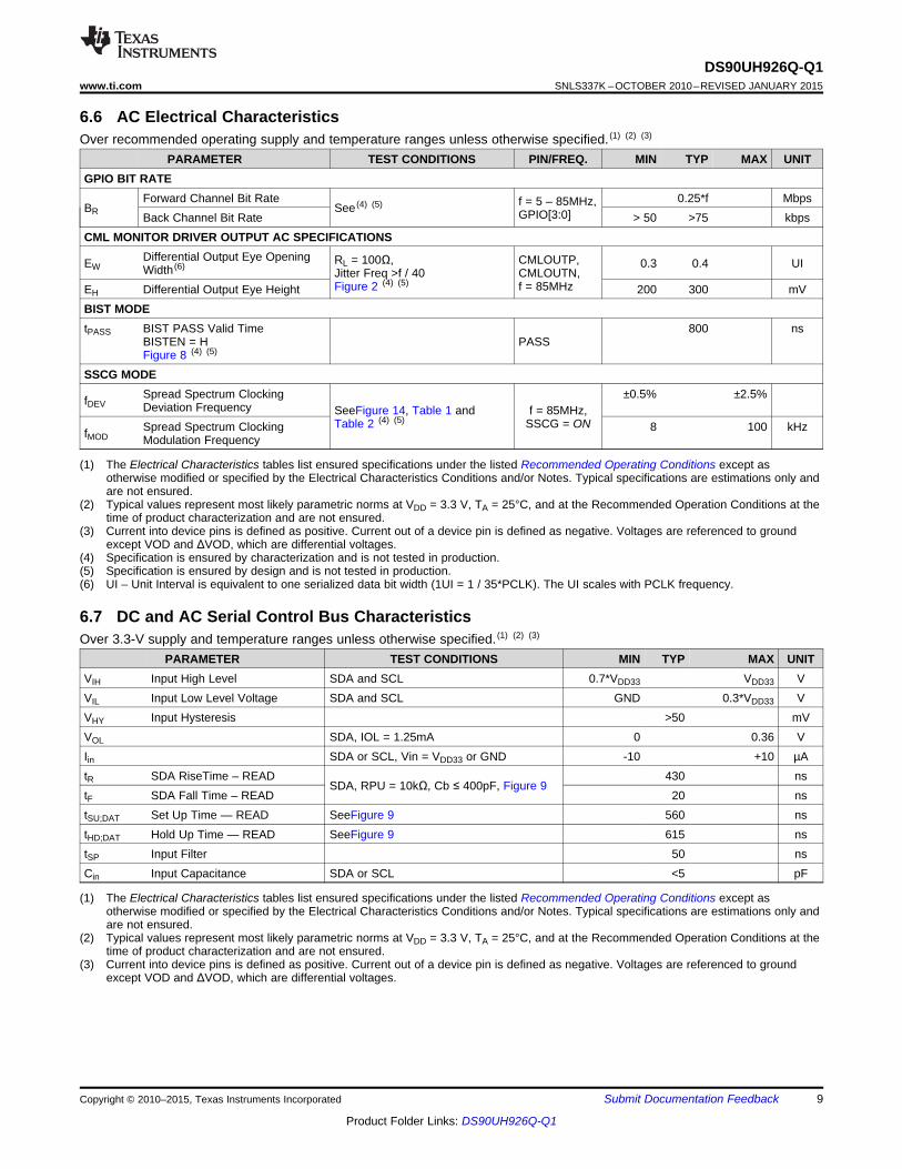
6.6 AC Electrical CharacteristicsOver recommended operating supply and temperature ranges unless otherwise specified. (1) (2) (3)
PARAMETER TEST CONDITIONS PIN/FREQ. MIN TYP MAX UNITGPIO BIT RATE
Forward Channel Bit Rate 0.25*f Mbpsf = 5 – 85MHz,BR See (4) (5)GPIO[3:0]Back Channel Bit Rate > 50 >75 kbps
CML MONITOR DRIVER OUTPUT AC SPECIFICATIONSDifferential Output Eye Opening RL = 100Ω, CMLOUTP,EW 0.3 0.4 UIWidth (6) Jitter Freq >f / 40 CMLOUTN,
Figure 2 (4) (5) f = 85MHzEH Differential Output Eye Height 200 300 mVBIST MODEtPASS BIST PASS Valid Time 800 ns
BISTEN = H PASSFigure 8 (4) (5)
SSCG MODESpread Spectrum Clocking ±0.5% ±2.5%fDEV Deviation Frequency SeeFigure 14, Table 1 and f = 85MHz,
Table 2 (4) (5) SSCG = ONSpread Spectrum Clocking 8 100 kHzfMOD Modulation Frequency
(1) The Electrical Characteristics tables list ensured specifications under the listed Recommended Operating Conditions except asotherwise modified or specified by the Electrical Characteristics Conditions and/or Notes. Typical specifications are estimations only andare not ensured.
(2) Typical values represent most likely parametric norms at VDD = 3.3 V, TA = 25°C, and at the Recommended Operation Conditions at thetime of product characterization and are not ensured.
(3) Current into device pins is defined as positive. Current out of a device pin is defined as negative. Voltages are referenced to groundexcept VOD and ΔVOD, which are differential voltages.
(4) Specification is ensured by characterization and is not tested in production.(5) Specification is ensured by design and is not tested in production.(6) UI – Unit Interval is equivalent to one serialized data bit width (1UI = 1 / 35*PCLK). The UI scales with PCLK frequency.
6.7 DC and AC Serial Control Bus CharacteristicsOver 3.3-V supply and temperature ranges unless otherwise specified. (1) (2) (3)
PARAMETER TEST CONDITIONS MIN TYP MAX UNITVIH Input High Level SDA and SCL 0.7*VDD33 VDD33 VVIL Input Low Level Voltage SDA and SCL GND 0.3*VDD33 VVHY Input Hysteresis >50 mVVOL SDA, IOL = 1.25mA 0 0.36 VIin SDA or SCL, Vin = VDD33 or GND -10 +10 µAtR SDA RiseTime – READ 430 ns
SDA, RPU = 10kΩ, Cb ≤ 400pF, Figure 9tF SDA Fall Time – READ 20 nstSU;DAT Set Up Time — READ SeeFigure 9 560 nstHD;DAT Hold Up Time — READ SeeFigure 9 615 nstSP Input Filter 50 nsCin Input Capacitance SDA or SCL <5 pF
(1) The Electrical Characteristics tables list ensured specifications under the listed Recommended Operating Conditions except asotherwise modified or specified by the Electrical Characteristics Conditions and/or Notes. Typical specifications are estimations only andare not ensured.
(2) Typical values represent most likely parametric norms at VDD = 3.3 V, TA = 25°C, and at the Recommended Operation Conditions at thetime of product characterization and are not ensured.
(3) Current into device pins is defined as positive. Current out of a device pin is defined as negative. Voltages are referenced to groundexcept VOD and ΔVOD, which are differential voltages.
Copyright © 2010–2015, Texas Instruments Incorporated Submit Documentation Feedback 9
Product Folder Links: DS90UH926Q-Q1

DS90UH926Q-Q1SNLS337K –OCTOBER 2010–REVISED JANUARY 2015 www.ti.com
6.8 Recommended Timing Requirements for the Serial Control BusOver 3.3-V supply and temperature ranges unless otherwise specified.
MIN NOM MAX UNITfSCL Standard Mode 0 100 kHz
SCL Clock FrequencyFast Mode 0 400 kHz
tLOW Standard Mode 4.7 µsSCL Low Period
Fast Mode 1.3 µstHIGH Standard Mode 4.0 µs
SCL High PeriodFast Mode 0.6 µs
tHD;STA Hold time for a start or a Standard Mode 4.0 µsrepeated start condition
Fast Mode 0.6 µsFigure 9tSU:STA Set Up time for a start or a Standard Mode 4.7 µs
repeated start conditionFast Mode 0.6 µsFigure 9
tHD;DAT Standard Mode 0 3.45 µsData Hold TimeFigure 9 Fast Mode 0 0.9 µs
tSU;DAT Standard Mode 250 nsData Set Up TimeFigure 9 Fast Mode 100 ns
tSU;STO Standard Mode 4.0 µsSet Up Time for STOPCondition, Figure 9 Fast Mode 0.6 µs
tBUF Bus Free Time Standard Mode 4.7 µsBetween STOP and START,
Fast Mode 1.3 µsFigure 9tr Standard Mode 1000 nsSCL & SDA Rise Time,
Figure 9 Fast Mode 300 nstf Standard Mode 300 nsSCL & SDA Fall Time,
Figure 9 Fast mode 300 ns
6.9 Switching Characteristicsover operating free-air temperature range (unless otherwise noted)
PARAMETER TEST CONDITIONS PIN/FREQ. MIN TYP MAX UNITtRCP PCLK Output Period tRCP = tTCP 11.76 T 200 ns
PCLKtRDC PCLK Output Duty Cycle 45% 50% 55%
VDDIO = 1.71 - 1.89 V, 2 3 nsLVCMOS Low-to-High Transition CL = 12pFtCLH Time
VDDIO = 3.0 – 3.6 V,Figure 3 2 3 nsCL = 12pFVDDIO = 1.71 - 1.89 V, R[7:0], G[7:0], 2 3 nsLVCMOS High-to-Low Transition CL = 12pF B[7:0], HS,tCHL Time VS, DE,VDDIO = 3.0 – 3.6 V,Figure 3 2 3 nsPCLK, LOCK,CL = 12pF
PASS, MCLK,VDDIO = 1.71 - 1.89 V,Data Valid before PCLK – Setup I2S_CLK, 2.2 nsCL = 12pFTime I2S_WC,tROS SSCG = OFF I2S_DA,VDDIO = 3.0 – 3.6 V, 2.2 nsFigure 6 I2S_DBCL = 12pFVDDIO = 1.71 - 1.89 V,Data Valid after PCLK – Hold 3.0 nsCL = 12pFTimetROH SSCG = OFF VDDIO = 3.0 – 3.6 V, 3.0 nsFigure 6 CL = 12pF
10 Submit Documentation Feedback Copyright © 2010–2015, Texas Instruments Incorporated
Product Folder Links: DS90UH926Q-Q1

GND
VDDIO
GND
VDDIORGB[n] (odd),
VS, HS
PCLK
RGB[n] (even),DE GND
VDDIO
DS90UH926Q-Q1www.ti.com SNLS337K –OCTOBER 2010–REVISED JANUARY 2015
Switching Characteristics (continued)over operating free-air temperature range (unless otherwise noted)
PARAMETER TEST CONDITIONS PIN/FREQ. MIN TYP MAX UNITR[7:0], G[7:0], 10 nsB[7:0]HS, VS, DE,PCLK, LOCK, 15 ns
Active to OFF Delay PASStXZR OEN = L, OSS_SEL = HFigure 5 (1) (2)MCLK,I2S_CLK,I2S_WC, 60 nsI2S_DA,I2S_DB
Lock TimetDDLT SSCG = OFF f = 5 – 85MHz 5 40 msFigure 5 (1) (2) (3)
tDD Delay – Latency (1) (2) f = 5 – 85MHz 147*T nsf = 5 – <15 0.5 nsMHzf = 15 – 85tDCCJ Cycle-to-Cycle Jitter (1) (2) SSCG = OFF 0.2 nsMHzI2S_CLK = 1 - ±2 ns12.28MHz
VDDIO = 1.71 - 1.89 V, 50 nsData Valid After OEN = H CL = 12pFtONS SetupTime
VDDIO = 3.0 – 3.6 V,Figure 7 (1) (2) 50 nsCL = 12pFVDDIO = 1.71 - 1.89 V, 50 nsR[7:0], G[7:0],Data Tri-State After OEN = L CL = 12pF
B[7:0], HS,tONH SetupTimeVDDIO = 3.0 – 3.6 V, VS, DE,Figure 7 (1) (2) 50 nsCL = 12pF PCLK, MCLK,
I2S_CLK,VDDIO = 1.71 - 1.89 V, 5 nsData Tri-State after OSS_ SEL = I2S_WC,CL = 12pFtSES H, Setup Time I2S_DA,
VDDIO = 3.0 – 3.6 V,Figure 7 (1) (2) I2S_DB 5 nsCL = 12pFVDDIO = 1.71 - 1.89 V, 5 nsData to Low after OSS_SEL = L CL = 12pF
tSEH Setup TimeVDDIO = 3.0 – 3.6 V,Figure 7 (1) (2) 5 nsCL = 12pF
(1) Specification is ensured by characterization and is not tested in production.(2) Specification is ensured by design and is not tested in production.(3) tDDLT is the time required by the device to obtain lock when exiting power-down state with an active serial stream.
Figure 1. Checker Board Data Pattern
Copyright © 2010–2015, Texas Instruments Incorporated Submit Documentation Feedback 11
Product Folder Links: DS90UH926Q-Q1

RIN(Diff.)
Z or L or PU
Z or L
Z or L
TRI-STATE or LOW or Pulled Up
TRI-STATE or LOW
RGB[7:0],HS, VS, DE,
I2S
PCLK(RFB = L)
TRI-STATEor LOW
LOCK
v[
tXZR
tDDLT
PDB 2.0V
0.8V
IN LOCK TIMEOFF ACTIVE OFF
33210
STARTBIT
STOPBIT
SYMBOL N+1
33210
STARTBIT
STOPBIT
SYMBOL N
RIN
(Diff.)
PCLK(RFB = L)
tDD
RGB[7:0], I2S[2:0],
HS, VS, DE
SYMBOL N-1 SYMBOL NSYMBOL N-2
80%
VDDIO
20%
tCLH tCHL
GND
CMLOUT(Diff.)
VOD (+)
tBIT (1 UI)
EW
VOD (-)
0VEH
EH
DS90UH926Q-Q1SNLS337K –OCTOBER 2010–REVISED JANUARY 2015 www.ti.com
Figure 2. CML Output Driver
Figure 3. LVCMOS Transition Times
Figure 4. Delay - Latency
Figure 5. PLL Lock Times and PDB TRI-STATE Delay
12 Submit Documentation Feedback Copyright © 2010–2015, Texas Instruments Incorporated
Product Folder Links: DS90UH926Q-Q1

BISTEN 1/2 VDDIO
PASS(w/errors)
tPASS
1/2 VDDIO
Prior BIST Result Current BIST Test - Toggle on Error Result Held
RIN(Diff.)
TRI-STATE
LOW
RGB[7:0],HS, VS, DE,
I2S[2:0]
PCLK(RFB = L)
LOCK
v[
tONS
PDB = H
VIH
VIL
VIH
OEN
OSS_SEL
PASS
TRI-STATE
LOW
HIGH
ACTIVE
ACTIVE
ACTIVE
VIL
TRI-STATE
TRI-STATELOW
LOW
HIGH
(HIGH)
tSES
tSEH
tONH
TRI-STATE
1/2 VDDIO
GND
VDDIO
GND
VDDIO
tROS tROH
PCLKw/RFB = H
RGB[7:0],VS, HS, DE,
I2S
VOHmin
VOLmax
DS90UH926Q-Q1www.ti.com SNLS337K –OCTOBER 2010–REVISED JANUARY 2015
Figure 6. Output Data Valid (Setup and Hold) Times With SSCG = OFF
Figure 7. Output State (Setup and Hold) Times
Figure 8. BIST PASS Waveform
Copyright © 2010–2015, Texas Instruments Incorporated Submit Documentation Feedback 13
Product Folder Links: DS90UH926Q-Q1
78 MHz TX Pixel Clock
Input (2 V/DIV)
78 MHz RX Pixel Clock
Output (2 V/DIV)
Time (10 ns/DIV)
Time (1.25 ns/DIV)
CM
L S
eria
lizer
Dat
a T
hrou
ghpu
t(2
00 m
V/D
IV)
SCL
SDA
tHD;STA
tLOW
tr
tHD;DAT
tHIGH
tf
tSU;DAT
tSU;STA tSU;STO
tf
START REPEATEDSTART
STOP
tHD;STA
START
tSP
trBUFt
DS90UH926Q-Q1SNLS337K –OCTOBER 2010–REVISED JANUARY 2015 www.ti.com
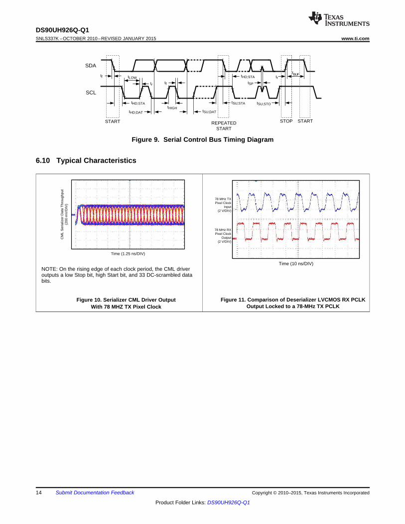
Figure 9. Serial Control Bus Timing Diagram
6.10 Typical Characteristics
NOTE: On the rising edge of each clock period, the CML driveroutputs a low Stop bit, high Start bit, and 33 DC-scrambled databits.
Figure 11. Comparison of Deserializer LVCMOS RX PCLKFigure 10. Serializer CML Driver OutputOutput Locked to a 78-MHz TX PCLKWith 78 MHZ TX Pixel Clock
14 Submit Documentation Feedback Copyright © 2010–2015, Texas Instruments Incorporated
Product Folder Links: DS90UH926Q-Q1

C1
C0
RIN-
RIN+
Clock and Data
Recovery
Timing and Control
24
LOCK
PCLK
SSCG
Out
put L
atch
Ser
ial t
o P
aral
lel
DC
Bal
ance
Dec
oder
PASS
RGB [7:0]
HSVSDE
ErrorDetector
PDB
BISTEN BISTC
CMF
SCLSCA
IDx
4 I2S_CLKI2S_WC I2S_DAMCLK
CMLOUTPCMLOUTN
HD
CP
Cip
her
MODE_SEL
REGULATOR
DS90UH926Q-Q1www.ti.com SNLS337K –OCTOBER 2010–REVISED JANUARY 2015
7 Detailed Description
7.1 OverviewThe DS90UH926Q-Q1 deserializer receives a 35-bits symbol over a single serial FPD-Link III pair operating upto a 2.975-Gbps application payload. The serial stream contains an embedded clock, video control signals andthe DC-balanced video data and audio data which enhance signal quality to support AC coupling.
The DS90UH926Q-Q1 deserializer attains lock to a data stream without the use of a separate reference clocksource, which greatly simplifies system complexity and overall cost. The deserializer also synchronizes to theserializer regardless of the data pattern, delivering true automatic “plug and lock” performance. It can lock to theincoming serial stream without the need of special training patterns or sync characters. The deserializer recoversthe clock and data by extracting the embedded clock information, validating then deserializing the incoming datastream. It also applies decryption through a High-Bandwidth Digital Content Protection (HDCP) Cipher to thisvideo and audio data stream following reception of the data from the FPD-Link III decoder. The decrypted parallelLVCMOS video bus is provided to the display. The deserializer is intended for use with the DS90UH925Qserializer, but is also backward-compatible with DS90UR905Q or DS90UR907Q FPD-Link II serializer.
7.2 Functional Block Diagram
7.3 Feature Description
7.3.1 High-Speed Forward Channel Data TransferThe High-Speed Forward Channel (HS_FC) is composed of 35 bits of data containing RGB data, sync signals,HDCP, I2C, and I2S audio transmitted from Serializer to Deserializer. Figure 12 illustrates the serial stream perPCLK cycle. This data payload is optimized for signal transmission over an AC-coupled link. Data is randomized,balanced and scrambled.
Figure 12. FPD-Link III Serial Stream
The device supports clocks in the range of 5 MHz to 85 MHz. The application payload rate is 2.975 Gbpsmaximum (175 Mbps minimum) with the actual line rate of 2.975 Gbps maximum and 525 Mbps Minimum.
Copyright © 2010–2015, Texas Instruments Incorporated Submit Documentation Feedback 15
Product Folder Links: DS90UH926Q-Q1

PCLK IN
PCLK OUT
HS/VS/DE IN
HS/VS/DE OUT
Latency
Pulses 1 or 2 PCLKs wide
Filetered OUT
DS90UH926Q-Q1SNLS337K –OCTOBER 2010–REVISED JANUARY 2015 www.ti.com
Feature Description (continued)7.3.2 Low-Speed Back Channel Data TransferThe Low-Speed Backward Channel (LS_BC) of the DS90UH926Q-Q1 provides bidirectional communicationbetween the display and host processor. The information is carried back from the Deserializer to the Serializerper serial symbol. The back channel control data is transferred over the single serial link along with the high-speed forward data, DC balance coding and embedded clock information. This architecture provides a backwardpath across the serial link together with a high-speed forward channel. The back channel contains the I2C,HDCP, CRC and 4 bits of standard GPIO information with 10-Mbps line rate.
7.3.3 Backward Compatible ModeThe DS90UH926Q-Q1 is also backward-compatible to DS90UR905Q and DS90UR907Q FPD Link II serializerswith 15 - 65 MHz pixel clock frequencies supported. It receives 28-bits of data over a single serial FPD-Link IIpair operating at the line rate of 420 Mbps to 1.82 Gbps. This backward-compatible mode is provided through theMODE_SEL pin (Table 9) or the configuration register (Table 11). When backward compatible mode = ON, setLFMODE = 0.
7.3.4 Input Equalization GainFPD-Link III input adaptive equalizer provides compensation for transmission medium losses and reduces themedium-induced deterministic jitter. It equalizes up to 10-m STP cables with 3 connection breaks at maximumserialized stream payload rate of 2.975 Gbps.
7.3.5 Common Mode Filter Pin (CMF)The deserializer provides access to the center tap of the internal termination. A capacitor must be placed on thispin for additional common-mode filtering of the differential pair. This can be useful in high noise environments foradditional noise rejection capability. A 0.1-μF capacitor has to be connected to this pin to Ground.
7.3.6 Video Control Signal FilterWhen operating the devices in Normal Mode, the Video Control Signals (DE, HS, VS) have the followingrestrictions:• Normal Mode with Control Signal Filter Enabled: DE and HS — Only 2 transitions per 130 clock cycles are
transmitted, the transition pulse must be 3 PCLK or longer.• Normal Mode with Control Signal Filter Disabled: DE and HS — Only 2 transitions per 130 clock cycles are
transmitted, no restriction on minimum transition pulse.• VS — Only 1 transition per 130 clock cycles are transmitted, minimum pulse width is 130 clock cycles.
Video Control Signals are defined as low-frequency signals with limited transitions. Glitches of a control signalcan cause a visual display error. This feature allows for the chipset to validate and filter out any high-frequencynoise on the control signals. See Figure 13.
Figure 13. Video Control Signal Filter Waveform
16 Submit Documentation Feedback Copyright © 2010–2015, Texas Instruments Incorporated
Product Folder Links: DS90UH926Q-Q1

fdev(max)FPCLK+
Frequency
Time
FPCLK-
FPCLK
fdev(min)
1/fmod
DS90UH926Q-Q1www.ti.com SNLS337K –OCTOBER 2010–REVISED JANUARY 2015
Feature Description (continued)7.3.7 EMI Reduction Features
7.3.7.1 Spread Spectrum Clock Generation (SSCG)The DS90UH926Q-Q1 provides an internally-generated spread spectrum clock (SSCG) to modulate its outputs.Both clock and data outputs are modulated. This will aid to lower system EMI. Output SSCG deviations to ±2.5%(5% total) at up to 100-kHz modulations are available. This feature may be controlled by register. See Table 1,Table 2 and Table 11. Do not enable the SSCG feature if the source PCLK into the SER has a clock with spreadspectrum already.
Figure 14. SSCG Waveform
Table 1. SSCG ConfigurationLFMODE = L (15 - 85 MHz)
SSCG CONFIGURATION (0x2C) LFMODE = L (15 - 85 MHz) SPREAD SPECTRUM OUTPUTSSC[2] SSC[1] SSC[0] Fdev (%) Fmod (kHz)
L L L ±0.9 PCLK / 2168L L H ±1.2L H L ±1.9L H H ±2.5H L L ±0.7 PCLK / 1300H L H ±1.3H H L ±2.0H H H ±2.5
Table 2. SSCG ConfigurationLFMODE = H (5 - <15 MHz)
SSCG CONFIGURATION (0x2C) LFMODE = H (5 - <15 MHz) SPREAD SPECTRUM OUTPUTSSC[2] SSC[1] SSC[0] Fdev (%) Fmod (kHz)
L L L ±0.5 PCLK / 628L L H ±1.3L H L ±1.8L H H ±2.5H L L ±0.7 PCLK / 388H L H ±1.2H H L ±2.0H H H ±2.5
7.3.8 Enhanced Progressive Turn-On (EPTO)The deserializer LVCMOS parallel outputs timing are delayed. Groups of 8-bit R, G and B outputs switch in adifferent time. This minimizes the number of outputs switching simultaneously and helps to reduce supply noise.In addition it spreads the noise spectrum out reducing overall EMI.
Copyright © 2010–2015, Texas Instruments Incorporated Submit Documentation Feedback 17
Product Folder Links: DS90UH926Q-Q1

DS90UH926Q-Q1SNLS337K –OCTOBER 2010–REVISED JANUARY 2015 www.ti.com
7.3.9 LVCMOS VDDIO OptionThe deserializer parallel bus can operate with 1.8-V or 3.3-V levels (VDDIO) for target (Display) compatibility.The 1.8-V levels will offer a lower noise (EMI) and also a system power savings.
7.3.10 Power Down (PDB)The Serializer has a PDB input pin to ENABLE or POWER DOWN the device. This pin can be controlled by thehost or through the VDDIO, where VDDIO = 3.0V to 3.6V or VDD33. To save power disable the link when the displayis not needed (PDB = LOW). When the pin is driven by the host, make sure to release it after VDD33 and VDDIOhave reached final levels; no external components are required. In the case of driven by the VDDIO = 3.0 V to 3.6V or VDD33 directly, a 10-kΩ resistor to the VDDIO = 3.0 V to 3.6 V or VDD33 , and a >10-µF capacitor to the groundare required (See Figure 24).
7.3.11 Stop Stream SleepThe deserializer enters a low power SLEEP state when the input serial stream is stopped. A STOP condition isdetected when the embedded clock bits are not present. When the serial stream starts again, the deserializer willthen lock to the incoming signal and recover the data.
NOTEIn STOP STREAM SLEEP, the Serial Control Bus Registers values are retained.
7.3.12 Serial Link Fault DetectThe serial link fault detection is able to detect any of following 7 conditions1. cable open2. + to - short3. + short to GND4. - short to GND5. + short to battery6. - short to battery7. Cable is linked incorrectly
If any one of the fault conditions occurs, The Link Detect Status is 0 (cable is not detected) on the Serial ControlBus Register bit 0 of address 0x1C Table 11. The link errors can be monitored though Link Error Count of theSerial Control Bus Register bit [4:0] of address 0x41 Table 11.
7.3.13 Oscillator OutputThe deserializer provides an optional PCLK output when the input clock (serial stream) has been lost. This isbased on an internal oscillator. The frequency of the oscillator may be selected. This feature is controlled byregister Address 0x02, bit 5 (OSC Clock Enable). See Table 11.
7.3.14 Pixel Clock Edge Select (RFB)The RFB determines the edge that the data is strobed on. If RFB is High (‘1’), output data is strobed on theRising edge of the PCLK. If RFB is Low (‘0’), data is strobed on the Falling edge of the PCLK. This allows forinter-operability with downstream devices. The deserializer output does not need to use the same edge as theSer input. This feature may be controlled by register. See Table 11.
7.3.15 Built In Self Test (BIST)An optional At-Speed, Built-In Self Test (BIST) feature supports the testing of the high speed serial link and thelow- speed back channel. This is useful in the prototype stage, equipment production, in-system test and also forsystem diagnostics. The BIST is not available in backwards-compatible mode.
18 Submit Documentation Feedback Copyright © 2010–2015, Texas Instruments Incorporated
Product Folder Links: DS90UH926Q-Q1
DS90UH926Q-Q1www.ti.com SNLS337K –OCTOBER 2010–REVISED JANUARY 2015
7.3.15.1 BIST Configuration and StatusThe BIST mode is enabled at the deserializer by the Pin select (Pin 44 BISTEN and Pin 16 BISTC) orconfiguration register (Table 11) through the deserializer. When LFMODE = 0, the pin based configurationdefaults to external PCLK or 33 MHz internal Oscillator clock (OSC) frequency. In the absence of PCLK, the usercan select the desired OSC frequency (default 33 MHz or 25MHz) through the register bit. When LFMODE = 1,the pin based configuration defaults to external PCLK or 12.5MHz MHz internal Oscillator clock (OSC) frequency.
When BISTEN of the deserializer is high, the BIST mode enable information is sent to the serializer through theBack Channel. The serializer outputs a test pattern and drives the link at speed. The deserializer detects the testpattern and monitors it for errors. The PASS output pin toggles to flag any payloads that are received with 1- to35-bit errors.
The BIST status is monitored real time on PASS pin. The result of the test is held on the PASS output until reset(new BIST test or Power Down). A High on PASS indicates NO ERRORS were detected. A Low on PASSindicates one or more errors were detected. The duration of the test is controlled by the pulse width applied tothe deserializer BISTEN pin. This BIST feature also contains a Link Error Count and a Lock Status. If theconnection of the serial link is broken, then the link error count is shown in the register. When the PLL of thedeserializer is locked or unlocked, the lock status can be read in the register. See Table 11.
7.3.15.1.1 Sample BIST Sequence
See Figure 15 for the BIST mode flow diagram.1. For the DS90UH925Q-Q1 and DS90UH926Q-Q1 FPD-Link III chipset, BIST Mode is enabled through the
BISTEN pin of DS90UH926Q-Q1 FPD-Link III deserializer. The desired clock source is selected throughBISTC pin.
2. The DS90UH925Q-Q1 serializer is woken up through the back channel if it is not already on. The all zeropattern on the data pins is sent through the FPD-Link III to the deserializer. Once the serializer and thedeserializer are in BIST mode and the deserializer acquires Lock, the PASS pin of the deserializer goes highand BIST starts checking the data stream. If an error in the payload (1 to 35) is detected, the PASS pin willswitch low for one half of the clock period. During the BIST test, the PASS output can be monitored andcounted to determine the payload error rate.
3. To Stop the BIST mode, the deserializer BISTEN pin is set Low. The deserializer stops checking the data.The final test result is held on the PASS pin. If the test ran error free, the PASS output will be High. If therewas one or more errors detected, the PASS output will be Low. The PASS output state is held until a newBIST is run, the device is RESET, or Powered Down. The BIST duration is user controlled by the duration ofthe BISTEN signal.
4. The Link returns to normal operation after the deserializer BISTEN pin is low. Figure 16 shows the waveformdiagram of a typical BIST test for two cases. Case 1 is error free, and Case 2 shows one with multiple errors.In most cases it is difficult to generate errors due to the robustness of the link (differential data transmissionetc.), thus they may be introduced by greatly extending the cable length, faulting the interconnect, reducingsignal condition enhancements ( Rx Equalization).
Copyright © 2010–2015, Texas Instruments Incorporated Submit Documentation Feedback 19
Product Folder Links: DS90UH926Q-Q1

X XX
PCLK(RFB = L)
BISTEN(DES)
PASS
DATA(internal)
PASS
BIST Duration
Prior Result
BIST ResultHeld
PASS
FAIL
X = bit error(s)
ROUT[23:0]HS, VS, DE
DATA(internal)
Cas
e 1
- P
ass
Cas
e 2
- F
ail
Prior Result
Normal SSO BIST Test Normal
DE
S O
utpu
ts
BISTstart
BISTstop
BISTWait
Step 1: DES in BIST
Step 2: Wait, SER in BIST
Step 3: DES in Normal Mode - check PASS
Step 4: DES/SER in Normal
Normal
DS90UH926Q-Q1SNLS337K –OCTOBER 2010–REVISED JANUARY 2015 www.ti.com
Figure 15. BIST Mode Flow Diagram
7.3.15.2 Forward-Channel and Back-Channel Error CheckingWhile in BIST mode, the serializer stops sampling RGB input pins and switches over to an internal all-zeropattern. The internal all-zeroes pattern goes through scrambler, dc-balancing etc. and goes over the serial link tothe deserializer. The deserializer on locking to the serial stream compares the recovered serial stream with all-zeroes and records any errors in status registers and dynamically indicates the status on PASS pin. Thedeserializer then outputs a SSO pattern on the RGB output pins.
The back-channel data is checked for CRC errors once the serializer locks onto back-channel serial stream asindicated by link detect status (register bit 0x0C[0]). The CRC errors are recorded in an 8-bit register. Theregister is cleared when the serializer enters the BIST mode. As soon as the serializer exits BIST mode, thefunctional mode CRC register starts recording the CRC errors. The BIST mode CRC error register is active inBIST mode only and keeps the record of last BIST run until it clears or enters BIST mode again.
Figure 16. BIST Waveforms
20 Submit Documentation Feedback Copyright © 2010–2015, Texas Instruments Incorporated
Product Folder Links: DS90UH926Q-Q1

DS90UH926Q-Q1www.ti.com SNLS337K –OCTOBER 2010–REVISED JANUARY 2015
7.3.16 Image Enhancement FeaturesSeveral image enhancement features are provided. White balance LUTs allow the user to define and target thecolor temperature of the display. Adaptive Hi-FRC dithering enables the presentation of “true-color” images on an18–bit color display.
7.3.16.1 White BalanceThe White Balance feature enables similar display appearance when using LCDs from different vendors. Itcompensates for native color temperature of the display, and adjusts relative intensities of R, G, B to maintainspecified color temperature. Programmable control registers are used to define the contents of three LUTs (8-bitcolor value for Red, Green and Blue) for the white balance feature. The LUTs map input RGB values to newoutput RGB values. There are three LUTs, one LUT for each color. Each LUT contains 256 entries, 8-bits perentry with a total size of 6144 bits (3 x 256 x 8). All entries are readable and writable. Calibrated values areloaded into registers through the I2C interface (deserializer is a slave device). This feature may also be appliedto lower color depth applications such as 18–bit (666) and 16–bit (565). White balance is enabled and configuredthrough that serial control bus register.
7.3.16.1.1 LUT Contents
The user must define and load the contents of the LUT for each color (R,G,B). Regardless of the color depthbeing driven (888, 666, 656), the user must always provide contents for 3 complete LUTs - 256 colors x 8 bits x 3tables. Unused bits - LSBs -shall be set to 0 by the user.
When 24-bit (888) input data is being driven to a 24-bit display, each LUT (R, G and B) must contain 256 unique8-bit entries. The 8-bit white balanced data is then available at the output of the DS90UH926Q-Q1 deserializer,and driven to the display.
When 18-bit (666) input data is being driven to an 18-bit display, the white balance feature may be used in one oftwo ways. First, simply load each LUT with 256, 8-bit entries. Each 8-bit entry is a 6-bit value (6 MSBs) with the 2LSBs set to 00. Thus as total of 64 unique 6-bit white balance output values are available for each color (R, Gand B). The 6-bit white balanced data is available at the output of the DS90UH926Q-Q1 deserializer, and drivendirectly to the display.
Alternatively, with 6-bit input data the user may choose to load complete 8-bit values into each LUT. This modeof operation provides the user with finer resolution at the LUT output to more closely achieve the desired whitepoint of the calibrated display. Although 8-bit data is loaded, only 64 unique 8-bit white balance output values areavailable for each color (R, G and B). The result is 8-bit white balanced data. Before driving to the output of thedeserializer, the 8-bit data must be reduced to 6-bit with an FRC dithering function. To operate in this mode, theuser must configure the DS90UH926Q-Q1 to enable the FRC2 function.
Examples of the three types of LUT configurations described are shown in Figure 17
7.3.16.1.2 Enabling White Balance
The user must load all 3 LUTs prior to enabling the white balance feature. The following sequence must befollowed by the user.
To initialize white balance after power-on (Table 3):1. Load contents of all 3 LUTs . This requires a sequential loading of LUTs - first RED, second GREEN, third
BLUE. 256, 8-bit entries must be loaded to each LUT. Page registers must be set to select each LUT.2. Enable white balance.
By default, the LUT data may not be reloaded after initialization at power-on.
An option does exist to allow LUT reloading after power-on and initial LUT loading (as described above). Thisoption may only be used after enabling the white balance reload feature through the associated serial control busregister. In this mode the LUTs may be reloaded by the master controller through the I2C. This provides the userwith the flexibility to refresh LUTs periodically , or upon system requirements to change to a new set of LUTvalues. The host controller loads the updated LUT values through the serial bus interface. There is no need todisable the white balance feature while reloading the LUT data. Refreshing the white balance to the new set ofLUT data will be seamless - no interruption of displayed data.
It is important to note that initial loading of LUT values requires that all three LUTs be loaded sequentially. Whenreloading, partial LUT updates may be made.
Copyright © 2010–2015, Texas Instruments Incorporated Submit Documentation Feedback 21
Product Folder Links: DS90UH926Q-Q1

Gray levelEntry
Data Out(8-bits)
0 00000000b 0 00000000b 0 00000001b1 00000001b 1 N/A 1 N/A2 00000011b 2 N/A 2 N/A3 00000011b 3 N/A 3 N/A4 00000110b 4 00000100b 4 00000110b5 00000110b 5 N/A 5 N/A6 00000111b 6 N/A 6 N/A7 00000111b 7 N/A 7 N/A8 00001000b 8 00001000b 8 00001011b9 00001010b 9 N/A 9 N/A
10 00001001b 10 N/A 10 N/A11 00001011b 11 N/A 11 N/A
248 11111010b 248 11111000b 248 11111010b249 11111010b 249 N/A 249 N/A250 11111011b 250 N/A 250 N/A251 11111011b 251 N/A 251 N/A252 11111110b 252 11111100b 252 11111111b253 11111101b 253 N/A 253 N/A254 11111101b 254 N/A 254 N/A255 11111111b 255 N/A 255 N/A
6-bit in / 8 bit out6-bit in / 6 bit out8-bit in / 8 bit out
««««««
Gray levelEntry
Data Out(8-bits)
Gray levelEntry
Data Out(8-bits)
DS90UH926Q-Q1SNLS337K –OCTOBER 2010–REVISED JANUARY 2015 www.ti.com
Figure 17. White Balance LUT Configurations
Table 3. White Balance Register TablePAGE ADD ADD REGISTER BITS ACCES DEFAU FUNCTION DESCRIPTION
(dec) (hex) NAME S LT(hex)
0 42 0x2A White Balance 7:6 RW 0x00 Page Setting 00: Configuration RegistersControl 01: Red LUT
10: Green LUT11: Blue LUT
5 RW White Balance 0: White Balance DisableEnable 1: White Balance Enable
4 RW 0: Reload Disable1: Reload Enable
3:0 Reserved1 0 – 00 – FF White Balance FF:0 RW N/A Red LUT 256 8–bit entries to be applied to the Red
255 Red LUT subpixel data2 0 – 00 – FF White Balance FF:0 RW N/A Green LUT 256 8–bit entries to be applied to the Green
255 Green LUT subpixel data3 0 – 00 – FF White Balance FF:0 RW N/A Blue LUT 256 8–bit entries to be applied to the Blue
255 Blue LUT subpixel data
7.3.16.2 Adaptive HI-FRC DitheringThe Adaptive FRC Dithering Feature delivers product-differentiating image quality. It reduces 24-bit RGB (8 bitsper subpixel) to 18-bit RGB (6 bits per sub-pixel), smoothing color gradients, and allowing the flexibility to uselower cost 18-bit displays. FRC (Frame Rate Control) dithering is a method to emulate “missing” colors on alower color depth LCD display by changing the pixel color slightly with every frame. FRC is achieved bycontrolling on and off pixels over multiple frames (Temporal). Static dithering regulates the number of on and offpixels in a small defined pixel group (Spatial). The FRC module includes both Temporal and Spatial methods andalso Hi-FRC. Conventional FRC can display only 16,194,277 colors with 6-bit RGB source. “Hi-FRC” enables full(16,777,216) color on an 18-bit LCD panel. The “adaptive” FRC module also includes input pixel detection toapply specific Spatial dithering methods for smoother gray level transitions. When enabled, the lower LSBs ofeach RGB output are not active; only 18 bit data (6 bits per R,G and B) are driven to the display. This feature isenabled through the serial control bus register.
22 Submit Documentation Feedback Copyright © 2010–2015, Texas Instruments Incorporated
Product Folder Links: DS90UH926Q-Q1

Pixel Index PD1 PD2 PD3 PD4 PD5 PD6 PD7 PD8
LSB=001
F0L0 010 000 000 000 000 000 010 000
F0L1 101 000 000 000 101 000 000 000
F0L2 000 000 010 000 010 000 000 000
F0L3 000 000 101 000 000 000 101 000
F1L0 000 000 000 000 000 000 000 000
F1L1 000 111 000 000 000 111 000 000
F1L2 000 000 000 000 000 000 000 000
F1L3 000 000 000 111 000 000 000 111
F2L0 000 000 010 000 010 000 000 000
F2L1 000 000 101 000 000 000 101 000
F2L2 010 000 000 000 000 000 010 000
F2L3 101 000 000 000 101 000 000 000
F3L0 000 000 000 000 000 000 000 000
F3L1 000 000 000 111 000 000 000 111
F3L2 000 000 000 000 000 000 000 000
F3L3 000 111 000 000 000 111 000 000
R = 4/32
G = 4/32
B = 4/32
R = 4/32
G = 4/32
B = 4/32
R = 4/32
G = 4/32
B = 4/32
R = 4/32
G = 4/32
B = 4/32
LSB=001 three lsb of 9 bit data (8 to 9 for Hi-Frc)
F0L0
PD1
Cell Value 010
Frame = 0, Line = 0
Pixel Data one
R[7:2]+0, G[7:2]+1, B[7:2]+0
LSB = 001
DS90UH926Q-Q1www.ti.com SNLS337K –OCTOBER 2010–REVISED JANUARY 2015
Two FRC functional blocks are available, and may be independently enabled. FRC1 precedes the white balanceLUT, and is intended to be used when 24-bit data is being driven to an 18-bit display with a white balance LUTthat is calibrated for an 18-bit data source. The second FRC block, FRC2, follows the white balance block and isintended to be used when fine adjustment of color temperature is required on an 18-bit color display, or when a24-bit source drives an 18-bit display with a white balance LUT calibrated for 24-bit source data.
For proper operation of the FRC dithering feature, the user must provide a description of the display timingcontrol signals. The timing mode, “sync mode” (HS, VS) or “DE only” must be specified, along with the activepolarity of the timing control signals. All this information is entered to DS90UH926Q-Q1 control registers throughthe serial bus interface.
Adaptive Hi-FRC dithering consists of several components. Initially, the incoming 8-bit data is expanded to 9-bitdata. This allows the effective dithered result to support a total of 16.7 million colors. The incoming 9-bit data isevaluated, and one of four possible algorithms is selected. The majority of incoming data sequences aresupported by the default dithering algorithm. Certain incoming data patterns (black/white pixel, full on/off sub-pixel) require special algorithms designed to eliminate visual artifacts associated with these specific gray leveltransitions. Three algorithms are defined to support these critical transitions.
An example of the default dithering algorithm is illustrated in Figure 18. The 1 or 0 value shown in the tabledescribes whether the 6-bit value is increased by 1 (1) or left unchanged (0). In this case, the 3 truncated LSBsare 001.
Figure 18. Default FRC Algorithm
Table 4. Recommended FRC SettingsSOURCE WHITE BALANCE LUT DISPLAY FRC1 FRC2
24–bit 24–bit 24–bit Disabled Disabled24–bit 24–bit 18–bit Disabled Enabled24–bit 18–bit 18–bit Enabled Disabled18–bit 24–bit 24–bit Disabled Disabled
Copyright © 2010–2015, Texas Instruments Incorporated Submit Documentation Feedback 23
Product Folder Links: DS90UH926Q-Q1

DS90UH926Q-Q1SNLS337K –OCTOBER 2010–REVISED JANUARY 2015 www.ti.com
Table 4. Recommended FRC Settings (continued)SOURCE WHITE BALANCE LUT DISPLAY FRC1 FRC2
18–bit 24–bit 18–bit Disabled Enabled18–bit 18–bit 18–bit Disabled Disabled
7.3.17 Internal Pattern GenerationThe DS90UH926Q-Q1 serializer supports the internal pattern generation feature. It allows basic testing anddebugging of an integrated panel. The test patterns are simple and repetitive and allow for a quick visualverification of panel operation. As long as the device is not in power down mode, the test pattern will bedisplayed even if no parallel input is applied. If no PCLK is received, the test pattern can be configured to use aprogrammed oscillator frequency. For detailed information, refer to AN-2198 Exploring the Internal Test PatternGeneration Feature of 720p FPD-Link III Devices (SNLA132).
7.3.18 I2S ReceivingIn normal 24-bit RGB operation mode, the DS90UH926Q-Q1 provides up to 3-bit of I2S. They are I2S_CLK,I2S_WC and I2S_DA, as well as the Master I2S Clock (MCLK). The encrypted and packetized audio informationis received during the video blanking periods along with specific information about the clock frequency. The bitrates of any I2S input bits must maintain one fourth of the PCLK rate. The audio decryption is supported perHDCP v1.3. A jitter cleaning feature reduces I2S_CLK output jitter to ±2ns.
7.3.18.1 I2S Jitter CleaningThe DS90UH926Q-Q1 features a standalone PLL to clean the I2S data jitter supporting high end car audiosystems. If I2S CLK frequency is less than 1 MHz, this feature has to be disabled through the register bit I2SControl (0x2B) in Table 11.
7.3.18.2 Secondary I2S ChannelIn 18-bit RGB operation mode, the secondary I2S data (I2S_DB) can be used as the additional I2S audiochannel in additional to the 3–bit of I2S. The I2S_DB is synchronized to the I2S_CLK. To enable thissynchronization feature on this bit, set the MODE_SEL (Table 9) or program through the register bit (Table 11).
7.3.18.3 MCLKThe deserializer has an I2S Master Clock Output. It supports x1, x2, or x4 of I2S CLK Frequency. When the I2SPLL is disabled, the MCLK output is OFF. Table 5 below covers the range of I2S sample rates and MCLKfrequencies.
By default, all the MCLK output frequencies are x2 of the I2S CLK frequencies. The MCLK frequencies can alsobe enabled through the register bit [7:4] (I2S MCLK Output) of 0x3A shown in Table 11. To select desired MCLKfrequency, write bit 7 (0x3A) = 1, then write to bit [6:4] accordingly.
Table 5. Audio Interface FrequenciesSAMPLE RATE I2S DATA WORD SIZE I2S CLK MCLK OUTPUT BIT [6:4]
(kHz) (bits) (MHz) (MHz) (ADDRESS 0x3A)x1 of I2S CLK 000
32 16 1.024 x2 of I2S CLK 001x4 of I2S CLK 010x1 of I2S CLK 000
44.1 16 1.411 x2 of I2S CLK 001x4 of I2S CLK 010x1 of I2S CLK 000
48 16 1.536 x2 of I2S CLK 001x4 of I2S CLK 010
24 Submit Documentation Feedback Copyright © 2010–2015, Texas Instruments Incorporated
Product Folder Links: DS90UH926Q-Q1

DS90UH926Q-Q1www.ti.com SNLS337K –OCTOBER 2010–REVISED JANUARY 2015
Table 5. Audio Interface Frequencies (continued)SAMPLE RATE I2S DATA WORD SIZE I2S CLK MCLK OUTPUT BIT [6:4]
(kHz) (bits) (MHz) (MHz) (ADDRESS 0x3A)x1 of I2S CLK 001
96 16 3.072 x2 of I2S CLK 010x4 of I2S CLK 011x1 of I2S CLK 010
192 16 6.144 x2 of I2S CLK 011x4 of I2S CLK 100x1 of I2S CLK 000
32 24 1.536 x2 of I2S CLK 001x4 of I2S CLK 010x1 of I2S CLK 001
44.1 24 2.117 x2 of I2S CLK 010x4 of I2S CLK 011x1 of I2S CLK 001
48 24 2.304 x2 of I2S CLK 010x4 of I2S CLK 011x1 of I2S CLK 010
96 24 4.608 x2 of I2S CLK 011x4 of I2S CLK 100x1 of I2S CLK 011
192 24 9.216 x2 of I2S CLK 100x4 of I2S CLK 101x1 of I2S CLK 001
32 32 2.048 x2 of I2S CLK 010x4 of I2S CLK 011x1 of I2S CLK 001
44.1 32 2.822 x2 of I2S CLK 010x4 of I2S CLK 011x1 of I2S CLK 001
48 32 3.072 x2 of I2S CLK 010x4 of I2S CLK 011x1 of I2S CLK 010
96 32 6.144 x2 of I2S CLK 011x4 of I2S CLK 100x1 of I2S CLK 011
192 32 12.288 x2 of I2S CLK 100x4 of I2S CLK 110
7.3.19 Interrupt Pin: Functional Description and Usage (INTB)1. On DS90UH925Q-Q1, set register 0xC6[5] = 1 and 0xC6[0] = 12. DS90UH926Q-Q1 deserializer INTB_IN (pin 16) is set LOW by some downstream device.3. DS90UH925Q-Q1 serializer pulls INTB (pin 31) LOW. The signal is active low, so a LOW indicates an
interrupt condition.4. External controller detects INTB = LOW; to determine interrupt source, read HDCP_ISR register .5. A read to HDCP_ISR will clear the interrupt at the DS90UH925, releasing INTB.6. The external controller typically must then access the remote device to determine downstream interrupt
source and clear the interrupt driving INTB_IN. This would be when the downstream device releases theINTB_IN (pin 16) on the DS90UH926Q-Q1. The system is now ready to return to step (1) at next falling edge
Copyright © 2010–2015, Texas Instruments Incorporated Submit Documentation Feedback 25
Product Folder Links: DS90UH926Q-Q1

DS90UH926Q-Q1SNLS337K –OCTOBER 2010–REVISED JANUARY 2015 www.ti.com
of INTB_IN.
7.3.20 GPIO[3:0] and GPO_REG[8:4]In 18-bit RGB operation mode, the optional R[1:0] and G[1:0] of the DS90UH926Q-Q1 can be used as thegeneral purpose IOs GPIO[3:0] in either forward channel (Outputs) or back channel (Inputs) application.
GPIO[3:0] Enable SequenceSee Table 6 for the GPIO enable sequencing.1. Enable the 18-bit mode either through the configuration register bit Table 11 on DS90UH925Q-Q1 only.
DS90UH926Q-Q1 is automatically configured as in the 18-bit mode.2. To enable GPIO3 forward channel, write 0x03 to address 0x0F on DS90UH925Q-Q1, then write 0x05 to
address 0x1F on DS90UH926Q-Q1.
Table 6. GPIO Enable Sequencing TableNO. DESCRIPTION DEVICE FORWARD CHANNEL BACK CHANNEL
1 Enable 18-bit DS90UH925Q-Q1 0x12 = 0x04 0x12 = 0x04mode DS90UH926Q-Q1 Auto Load from DS90UH925Q-Q1 Auto Load from DS90UH925Q-Q1
2 GPIO3 DS90UH925Q-Q1 0x0F = 0x03 0x0F = 0x05DS90UH926Q-Q1 0x1F = 0x05 0x1F = 0x03
3 GPIO2 DS90UH925Q-Q1 0x0E = 0x30 0x0E = 0x50DS90UH926Q-Q1 0x1E = 0x50 0x1E = 0x30
4 GPIO1 DS90UH925Q-Q1 0x0E = 0x03 0x0E = 0x05DS90UH926Q-Q1 0x1E = 0x05 0x0E = 0x05
5 GPIO0 DS90UH925Q-Q1 0x0D = 0x93 0x0D = 0x95DS90UH926Q-Q1 0x1D = 0x95 0x1D = 0x93
7.3.20.1 GPO_REG[8:4] Enable SequenceGPO_REG[8:4] are the outputs only pins. They must be programmed through the local register bits. SeeTable 11 for the GPO_REG enable sequencing.1. Enable the 18-bit mode either through the configuration register bit Table 11 on DS90UH925Q-Q1 only.
DS90UH926Q-Q1 is automatically configured as in the 18-bit mode.2. To enable GPO_REG8 outputs a 1, write 0x90 to address 0x11 on DS90UH925Q.
Table 7. GPO_REG Enable Sequencing TableNO. DESCRIPTION DEVICE LOCAL ACCESS LOCAL OUTPUT VALUE
1 Enable 18-bit mode DS90UH926Q-Q1 0x12 = 0x04(on DS90UH925Q-Q1)
2 GPO_REG8 DS90UH926Q-Q1 0x21 = 0x90 “1”0x21 = 0x10 “0”
3 GPO_REG7 DS90UH926Q-Q1 0x21 = 0x09 “1”0x21 = 0x01 “0”
4 GPO_REG6 DS90UH926Q-Q1 0x20 = 0x90 “1”0x20 = 0x10 “0”
5 GPO_REG5 DS90UH926Q-Q1 0x20 = 0x09 “1”0x20 = 0x01 “0”
6 GPO_REG4 DS90UH926Q-Q1 0x1F = 0x90 “1”0x1F = 0x10 “0”
26 Submit Documentation Feedback Copyright © 2010–2015, Texas Instruments Incorporated
Product Folder Links: DS90UH926Q-Q1

DESR4
MODE_SEL
R3
VR4
VDD33
DS90UH926Q-Q1www.ti.com SNLS337K –OCTOBER 2010–REVISED JANUARY 2015
7.4 Device Functional Modes
7.4.1 Clock-Data Recovery Status Flag (LOCK), Output Enable (OEN) and Output State Select(OSS_SEL)
When PDB is driven HIGH, the CDR PLL begins locking to the serial input and LOCK is TRI-STATE or LOW(depending on the value of the OEN setting). After the DS90UH926Q-Q1 completes its lock sequence to theinput serial data, the LOCK output is driven HIGH, indicating valid data and clock recovered from the serial inputis available on the parallel bus and PCLK outputs. The State of the outputs are based on the OEN andOSS_SEL setting (Table 8) or register bit (Table 11). See Figure 7.
Table 8. Output StatesINPUTS OUTPUTSSerial PDB OEN OSS_SEL Lock Pass Data, GPIO, I2S CLKinputX 0 X X Z Z Z ZX 1 0 0 L or H L L LX 1 0 1 L or H Z Z ZStatic 1 1 0 L L L L/OSC (Register bit
enable)Static 1 1 1 L Previous Status L LActive 1 1 0 H L L LActive 1 1 1 H Valid Valid Valid
7.4.2 Low Frequency Optimization (LFMODE)The LFMODE is set through a register (Table 11) or MODE_SEL Pin 24 (Table 9). It controls the operatingfrequency of the deserializer. If LFMODE is Low (default), the PCLK frequency is between 15 MHz and 85 MHz.If LFMODE is High, the PCLK frequency is between 5 MHz and <15 MHz. Please note: when the deviceLFMODE is changed, a PDB reset is required.
7.4.3 Configuration Select (MODE_SEL)Configuration of the device may be done through the MODE_SEL input pin, or through the configuration registerbit. A pullup resistor and a pulldown resistor of suggested values may be used to set the voltage ratio of theMODE_SEL input (VR4) and VDD33 to select one of the other 10 possible selected modes. See Figure 19 andTable 9.
Figure 19. MODE_SEL Connection Diagram
Copyright © 2010–2015, Texas Instruments Incorporated Submit Documentation Feedback 27
Product Folder Links: DS90UH926Q-Q1

DS90UH926Q-Q1SNLS337K –OCTOBER 2010–REVISED JANUARY 2015 www.ti.com
Table 9. Configuration Select (MODE_SEL)NO. IDEAL IDEAL VR4 SUGGESTED SUGGESTED LFMODE (1) REPEATER (2) BACKWARD I2S CHANNEL
RATIO (V) RESISTOR R3 RESISTOR R4 COMPATIBLE BVR4/VDD33 kΩ (1% tol) kΩ (1% tol) (3) (18–bit
MODE) (4)
1 0 0 Open 40.2 or Any L L L L2 0.121 0.399 294 40.2 L L L H3 0.152 0.502 280 49.9 L H L L4 0.242 0.799 240 76.8 L H L H5 0.311 1.026 226 102 H L L L6 0.402 1.327 196 130 H L L H7 0.492 1.624 169 165 H H L L8 0.583 1.924 137 191 H H L H9 0.629 2.076 124 210 L L H L
(1) LFMODE:L = frequency range is 15 – 85 MHz (Default)H = frequency range is 5 – <15 MHz ¢
(2) Repeater:L = Repeater mode is OFF (Default)H = Repeater mode is ON
(3) Backward Compatible:L = Backward Compatible mode is OFF (Default)H = Backward Compatible mode is ON; SER = DS90UR905Q or DS90UR907Q
– frequency range = 15 - 65MHz, set LFMODE = L(4) I2S Channel B:
L = I2S Channel B mode is OFF, Normal 24-bit RGB Mode (Default)H = I2S Channel B mode is ON, 18-bit RGB Mode with I2S_DB Enabled. Note: use of GPIO(s) on unused inputs must be enabled by
register.
7.4.4 HDCP RepeaterWhen DS90UH925Q-Q1 and DS90UH926Q-Q1 are configured as the HDCP Repeater application, it provides amechanism to extend HDCP transmission over multiple links to multiple display devices. This repeaterapplication provides a mechanism to authenticate all HDCP Receivers in the system and distribute protectedcontent to the HDCP Receivers using the encryption mechanisms provided in the HDCP specification.
In this document, the DS90UH925Q-Q1 is referred to as the HDCP Transmitter or transmit port (TX), and theDS90UH926Q-Q1 is referred to as the HDCP Receiver (RX). Figure 20 shows the maximum configurationsupported for HDCP Repeater implementations using the DS90UH925Q-Q1 (TX) and DS90UH926Q-Q1 (RX).Two levels of HDCP Repeaters are supported with a maximum of three HDCP Transmitters per HDCP Receiver.
28 Submit Documentation Feedback Copyright © 2010–2015, Texas Instruments Incorporated
Product Folder Links: DS90UH926Q-Q1

TXSource
TX
TX
RX
1:3 Repeater
TX
TX
TX
RX
1:3 Repeater
TX
TX
TX
RX
1:3 Repeater
TX
TX
TX
RX
1:3 Repeater
TX
RX Display
RX Display
RX Display
RX Display
RX Display
RX Display
RX Display
RX Display
RX Display
DS90UH926Q-Q1www.ti.com SNLS337K –OCTOBER 2010–REVISED JANUARY 2015
Figure 20. HDCP Maximum Repeater Application
To support HDCP Repeater operation, the DS90UH926Q-Q1 Deserializer includes the ability to control thedownstream authentication process, assemble the KSV list for downstream HDCP Receivers, and pass the KSVlist to the upstream HDCP Transmitter. An I2C master within the DS90UH926Q-Q1 communicates with the I2Cslave within the DS90UH925Q-Q1 Serializer. The DS90UH925Q-Q1 Serializer handles authenticating with adownstream HDCP Receiver and makes status available through the I2C interface. The DS90UH926Q-Q1monitors the transmit port status for each DS90UH925Q-Q1 and reads downstream KSV and KSV list valuesfrom the DS90UH925Q-Q1.
In addition to the I2C interface used to control the authentication process, the HDCP Repeater implementationincludes two other interfaces. A parallel LVCMOS interface provides the unencrypted video data in 24-bit RGBformat and includes the DE/VS/HS control signals. In addition to providing the RGB video data, the parallelLVCMOS interface communicates control information and packetized audio data during video blanking intervals.A separate I2S audio interface may optionally be used to send I2S audio data between the HDCP Receiver andHDCP Transmitter in place of using the packetized audio over the parallel LVCMOS interface. All audio andvideo data is decrypted at the output of the HDCP Receiver and is re-encrypted by the HDCP Transmitter.
Figure 21 provides more detailed block diagram of a 1:2 HDCP repeater configuration.
Copyright © 2010–2015, Texas Instruments Incorporated Submit Documentation Feedback 29
Product Folder Links: DS90UH926Q-Q1

R[7:0]
G[7:0]
B[7:0]
DE
VS
HS
I2S_CLK
I2S_WC
I2S_DA
INTB_IN
SDA
SCL
DS90UH925Q-Q1
R[7:0]
G[7:0]
B[7:0]
DE
VS
HS
I2S_CLK
I2S_WC
I2S_DA
INTB
SDA
SCL
MODE_SEL
ID[x]
MODE_SEL
ID[x]
VDD33
VDD33VDD33
VDD33
VDD33
VDDIO
Optional
DS90UH926Q-Q1
I2CMaster
upstreamTransmitter
HDCP TransmitterDS90UH925Q-Q1
I2CSlave
HDCP ReceiverDS90UH926Q-Q1
ParallelLVCMOS
I2S Audio
I2C
HDCP TransmitterDS90UH925Q-Q1
I2CSlave
downstreamReceiverorRepeater
downstreamReceiverorRepeater
FPD-Link III interfaces
DS90UH926Q-Q1SNLS337K –OCTOBER 2010–REVISED JANUARY 2015 www.ti.com
Figure 21. HDCP 1:2 Repeater Configuration
7.4.4.1 Repeater ConnectionsThe HDCP Repeater requires the following connections between the HDCP Receiver and each HDCPTransmitter Figure 22.1. Video Data – Connect PCLK, RGB and control signals (DE, VS, HS).2. I2C – Connect SCL and SDA signals. Both signals should be pulled up to VDD33 with 4.7 kΩ resistors3. Audio – Connect I2S_CLK, I2S_WC, and I2S_DA signals.4. IDx pin – Each HDCP Transmitter and Receiver must have an unique I2C address.5. MODE_SEL pin – All HDCP Transmitter and Receiver must be set into the Repeater Mode.6. Interrupt pin– Connect DS90UH926Q-Q1 INTB_IN pin to DS90UH925Q-Q1 INTB pin. The signal must be
pulled up to VDDIO.
Figure 22. HDCP Repeater Connection Diagram
30 Submit Documentation Feedback Copyright © 2010–2015, Texas Instruments Incorporated
Product Folder Links: DS90UH926Q-Q1

HOSTor
Salve
SERor
DESSCL
SDA
4.7k 4.7k R2
SCL
SDA
To other Devices
IDx
VDD33
R1VDD33
VR2
DS90UH926Q-Q1www.ti.com SNLS337K –OCTOBER 2010–REVISED JANUARY 2015
7.5 Programming
7.5.1 Serial Control BusThe DS90UH926Q-Q1 is configured by the use of a serial control bus that is I2C protocol compatible. . Multipledeserializer devices may share the serial control bus since 16 device addresses are supported. Device addressis set through the R1 and R2 values on IDx pin. See Figure 23.
The serial control bus consists of two signals and a configuration pin. The SCL is a Serial Bus Clock Input /Output. The SDA is the Serial Bus Data Input / Output signal. Both SCL and SDA signals require an externalpull-up resistor to VDD33. For most applications a 4.7-k pullup resistor to VDD33 may be used. The resistor valuemay be adjusted for capacitive loading and data rate requirements. The signals are either pulled High, or drivenLow.
Figure 23. Serial Control Bus Connection
The configuration pin is the IDx pin. This pin sets one of 16 possible device addresses. A pullup resistor and apulldown resistor of suggested values may be used to set the voltage ratio of the IDx input (VR2) and VDD33 toselect one of the other 16 possible addresses. See Table 10.
Table 10. Serial Control Bus Addresses for IDxIdeal Ratio Ideal VR2 Suggested Resistor Suggested Resistor Address 8'bNO. Address 7'bVR2 / VDD33 (V) R1 kΩ (1% tol) R2 kΩ (1% tol) Appended
1 0 0 Open 40.2 or Any 0x2C 0x582 0.121 0.399 294 40.2 0x2D 0x5A3 0.152 0.502 280 49.9 0x2E 0x5C4 0.182 0.601 270 60.4 0x2F 0x5E5 0.212 0.700 267 71.5 0x30 0x606 0.242 0.799 240 76.8 0x31 0x627 0.273 0.901 243 90.9 0x32 0x648 0.310 1.023 226 102 0x33 0x669 0.356 1.175 210 115 0x34 0x68
10 0.402 1.327 196 130 0x35 0x6A11 0.447 1.475 182 147 0x36 0x6C12 0.492 1.624 169 165 0x37 0x6E13 0.538 1.775 154 180 0x38 0x7014 0.583 1.924 137 191 0x39 0x7215 0.629 2.076 124 210 0x3A 0x7416 0.727 2.399 90.9 243 0x3B 0x76
Copyright © 2010–2015, Texas Instruments Incorporated Submit Documentation Feedback 31
Product Folder Links: DS90UH926Q-Q1

DS90UH926Q-Q1SNLS337K –OCTOBER 2010–REVISED JANUARY 2015 www.ti.com
7.6 Register Maps
Table 11. Serial Control Bus RegistersADD ADD Register Bit(s) Register Default Function Descriptions(dec) (hex) Name Type (hex)
0 0x00 I2C Device ID 7:1 RW Device ID 7–bit address of DeserializerSee Table 9
0 RW ID Setting I2C ID Setting1: Register I2C Device ID (Overrides IDx pin)0: Device ID is from IDx pin
1 0x01 Reset 7 RW 0x04 Remote Remote Auto Power DownAuto Power 1: Power down when no forward channel link is detectedDown 0: Do not power down when no forward channel link is
detected6:3 Reserved.2 RW BC Enable Back channel enable
1: Enable0: Disable
1 RW Digital Reset the entire digital block including registersRESET1 This bit is self-clearing.
1: Reset0: Normal operation
0 RW Digital Reset the entire digital block except registersRESET0 This bit is self-clearing
1: Reset0: Normal operation
2 0x02 Configuration 7 RW 0x00 Output LVCMOS Output Enable.[0] Enable 1: Enable
0: Disable. Tri-state Outputs6 RW OEN and Overrides Output Enable Pin and Output State pin
OSS_SEL 1: Enable overrideOverride 0: Disable - no override
5 RW OSC Clock OSC Clock Output EnableEnable If loss of lock OSC clock is output onto PCLK
0: Disable1: Enable
4 RW Output OSS Select to Control Output State during Lock LowSleep State PeriodSelect 1: Enable(OSS_SEL) 0: Disable
3 RW Backward Backward Compatible (BC) mode set by MODE_SEL pinCompatible or register.select by 1: BC is set by register bit. Use register bit reg_0x02[2] topin or set BC Moderegister 0: Use MODE_SEL pin.control
2 RW Backward Backward compatible (BC) mode to DS90UR905Q orCompatible DS90UR907Q, if reg_0x02[3] = 1Mode 1: Backward compatible with DS90UR905Q orSelect DS90UR907Q
(Set LFMODE = 0)0: Backward Compatible is OFF (default)
1 RW LFMODE Frequency range is set by MODE_SEL pin or registerselect by 1: Frequency range is set by register. Use registerpin or bitreg_0x02[0] to set LFMODEregister 0: Frequency range is set by MODE_SEL pin.control
0 RW LFMODE Frequency range select1: PCLK range = 5 - <15 MHz, if reg_0x02[1] = 10: PCLK range = 15 - 85 MHz (default)
32 Submit Documentation Feedback Copyright © 2010–2015, Texas Instruments Incorporated
Product Folder Links: DS90UH926Q-Q1

DS90UH926Q-Q1www.ti.com SNLS337K –OCTOBER 2010–REVISED JANUARY 2015
Register Maps (continued)Table 11. Serial Control Bus Registers (continued)
ADD ADD Register Bit(s) Register Default Function Descriptions(dec) (hex) Name Type (hex)
3 0x03 Configuration 7 0xF0 Reserved.[1] 6 RW CRC CRC Generator Enable (Back Channel)
Generator 1: EnableEnable 0: Disable
5 Reserved4 RW Filter HS, VS, DE two clock filter When enabled, pulses less
Enable than two full PCLK cycles on the DE, HS, and VS inputswill be rejected1: Filtering enable0: Filtering disable
3 RW I2C Pass- I2C Pass-Through Modethrough 1: Pass-Through Enabled
0: Pass-Through Disabled2 RW Auto ACK ACK Select
1: Auto ACK enable0: Self ACK
1 Reserved0 RW RRFB Pixel Clock Edge Select
1: Parallel Interface Data is strobed on the Rising ClockEdge.0: Parallel Interface Data is strobed on the Falling ClockEdge.
4 0x04 BCC 7:1 RW 0xFE BCC The watchdog timer allows termination of a control channelWatchdog Watchdog transaction, if it fails to complete within a programmedControl Timer amount of time. This field sets the Bidirectional Control
Channel Watchdog Timeout value in units of 2milliseconds.This field should not be set to 0
0 RW BCC Disable Bidirectional Control Channel Watchdog TimerWatchdog 1: Disables BCC Watchdog Timer operationTimer 0: Enables BCC Watchdog Timer operation"Disable
5 0x05 I2C Control [1] 7 RW 0x2E I2C Pass I2C Pass-Through All TransactionsThrough All 1: Enabled
0: Disabled6:4 RW I2C SDA Internal I2C SDA Hold Time
Hold Time It configures the amount of internal hold time provided forthe SDA input relative to the SCL input. Units are 50 ns.
3:0 RW I2C Filter I2C Glitch Filter DepthDepth It configures the maximum width of glitch pulses on the
SCL and SDA inputs that will be rejected. Units are 5 ns.
Copyright © 2010–2015, Texas Instruments Incorporated Submit Documentation Feedback 33
Product Folder Links: DS90UH926Q-Q1

DS90UH926Q-Q1SNLS337K –OCTOBER 2010–REVISED JANUARY 2015 www.ti.com
Register Maps (continued)Table 11. Serial Control Bus Registers (continued)
ADD ADD Register Bit(s) Register Default Function Descriptions(dec) (hex) Name Type (hex)
6 0x06 I2C Control [2] 7 R 0x00 Forward Control Channel Sequence Error Detected It indicates aChannel sequence error has been detected in forward controlSequence channel. It this bit is set, an error may have occurred in theError control channel operation.
6 RW Clear It clears the Sequence Error Detect bitSequence This bit is not self-clearing.Error
5 Reserved4:3 RW SDA Output SDA Output Delay
Delay This field configures output delay on the SDA output.Setting this value will increase output delay in units of 50ns. Nominal output delay values for SCL to SDA are:00 : 250ns01: 300ns10: 350ns11: 400ns
2 RW Local Write Disable Remote Writes to Local Registers throughSerializer (Does not affect remote access to I2C slaves atDeserializer)1: Stop remote write to local device registers0: remote write to local device registers
1 RW I2C Bus Speed up I2C Bus Watchdog TimerTimer 1: Timer expires after approximately 50 msSpeed 0: Timer expires after approximately 1s
0 RW I2C Bus Disable I2C Bus Timer When the I2C Timer may be usedTimer to detect when the I2C bus is free or hung up following anDisable invalid termination of a transaction. If SDA is high and no
signalling occurs for approximately 1 s, the I2C bus isassumed to be free. If SDA is low and no signaling occurs,the device will try to clear the bus by driving 9 clocks onSCL
7 0x07 Remote 7:1 RW 0x18 Remote ID Remote IDDevice ID Configures the I2C Slave ID of the remote Serializer. A
value of 0 in this field disables I2C access to remoteSerializer. This field is automatically configured through theSerializer Forward Channel. Software may overwrite thisvalue, but should also set the FREEZE DEVICE ID bit toprevent overwriting by the Forward Channel.
0 RW Freeze Freeze Serializer Device IDDevice ID 1: Prevent auto-loading of the Serializer Device ID from the
Forward Channel. The ID will be frozen at the valuewritten.0: Update
8 0x08 SlaveID[0] 7:1 RW 0x00 Target 7-bit Remote Slave Device ID 0Slave Configures the physical I2C address of the remote I2CDevice ID0 Slave device attached to the remote Serializer. If an I2C
transaction is addressed to the Slave Alias ID0, thetransaction will be remapped to this address beforepassing the transaction across the Bidirectional ControlChannel to the Serializer.
0 Reserved9 0x09 SlaveID[1] 7:1 RW 0x00 Target 7-bit Remote Slave Device ID 1
Slave Configures the physical I2C address of the remote I2CDevice ID1 Slave device attached to the remote Serializer. If an I2C
transaction is addressed to the Slave Alias ID1, thetransaction will be remapped to this address beforepassing the transaction across the Bidirectional ControlChannel to the Serializer.
0 Reserved
34 Submit Documentation Feedback Copyright © 2010–2015, Texas Instruments Incorporated
Product Folder Links: DS90UH926Q-Q1

DS90UH926Q-Q1www.ti.com SNLS337K –OCTOBER 2010–REVISED JANUARY 2015
Register Maps (continued)Table 11. Serial Control Bus Registers (continued)
ADD ADD Register Bit(s) Register Default Function Descriptions(dec) (hex) Name Type (hex)
10 0x0A SlaveID[2] 7:1 RW 0x00 Target 7-bit Remote Slave Device ID 2Slave Configures the physical I2C address of the remote I2CDevice ID2 Slave device attached to the remote Serializer. If an I2C
transaction is addressed to the Slave Alias ID2, thetransaction will be remapped to this address beforepassing the transaction across the Bidirectional ControlChannel to the Serializer.
0 Reserved11 0x0B SlaveID[3] 7:1 RW 0x00 Target 7-bit Remote Slave Device ID 3
Slave Configures the physical I2C address of the remote I2CDevice ID3 Slave device attached to the remote Serializer. If an I2C
transaction is addressed to the Slave Alias ID3, thetransaction will be remapped to this address beforepassing the transaction across the Bidirectional ControlChannel to the Serializer.
0 Reserved12 0x0C SlaveID[4] 7:1 RW 0x00 Target 7-bit Remote Slave Device ID 4
Slave Configures the physical I2C address of the remote I2CDevice ID4 Slave device attached to the remote Serializer. If an I2C
transaction is addressed to the Slave Alias ID4, thetransaction will be remapped to this address beforepassing the transaction across the Bidirectional ControlChannel to the Serializer.
0 Reserved13 0x0D SlaveID[5] 7:1 RW 0x00 Target 7-bit Remote Slave Device ID 5
Slave Configures the physical I2C address of the remote I2CDevice ID5 Slave device attached to the remote Serializer. If an I2C
transaction is addressed to the Slave Alias ID5, thetransaction will be remapped to this address beforepassing the transaction across the Bidirectional ControlChannel to the Serializer.
0 Reserved14 0x0E SlaveID[6] 7:1 RW 0x00 Target 7-bit Remote Slave Device ID 6
Slave Configures the physical I2C address of the remote I2CDevice ID6 Slave device attached to the remote Serializer. If an I2C
transaction is addressed to the Slave Alias ID6, thetransaction will be remapped to this address beforepassing the transaction across the Bidirectional ControlChannel to the Serializer.
0 Reserved15 0x0F SlaveID[7] 7:1 RW 0x00 Target 7-bit Remote Slave Device ID 7
Slave Configures the physical I2C address of the remote I2CDevice ID7 Slave device attached to the remote Serializer. If an I2C
transaction is addressed to the Slave Alias ID7, thetransaction will be remapped to this address beforepassing the transaction across the Bidirectional ControlChannel to the Serializer.
0 Reserved16 0x10 SlaveAlias[0] 7:1 RW 0x00 ID[0] Match 7-bit Remote Slave Device Alias ID 0
Configures the decoder for detecting transactionsdesignated for an I2C Slave device attached to the remoteSerializer. The transaction will be remapped to the addressspecified in the Slave ID0 register.A value of 0 in this field disables access to the remote I2CSlave.
0 Reserved
Copyright © 2010–2015, Texas Instruments Incorporated Submit Documentation Feedback 35
Product Folder Links: DS90UH926Q-Q1

DS90UH926Q-Q1SNLS337K –OCTOBER 2010–REVISED JANUARY 2015 www.ti.com
Register Maps (continued)Table 11. Serial Control Bus Registers (continued)
ADD ADD Register Bit(s) Register Default Function Descriptions(dec) (hex) Name Type (hex)
17 0x11 SlaveAlias[1] 7:1 RW 0x00 ID[1] Match 7-bit Remote Slave Device Alias ID 1Configures the decoder for detecting transactionsdesignated for an I2C Slave device attached to the remoteSerializer. The transaction will be remapped to the addressspecified in the Slave ID1 register.A value of 0 in this field disables access to the remote I2CSlave.
0 Reserved18 0x12 SlaveAlias[2] 7:1 RW 0x00 ID[2] Match 7-bit Remote Slave Device Alias ID 2
Configures the decoder for detecting transactionsdesignated for an I2C Slave device attached to the remoteSerializer. The transaction will be remapped to the addressspecified in the Slave ID2 register.A value of 0 in this field disables access to the remote I2CSlave.
0 Reserved19 0x13 SlaveAlias[3] 7:1 RW 0x10 ID[3] Match 7-bit Remote Slave Device Alias ID 3
Configures the decoder for detecting transactionsdesignated for an I2C Slave device attached to the remoteSerializer. The transaction will be remapped to the addressspecified in the Slave ID3 register.A value of 0 in this field disables access to the remote I2CSlave.
0 Reserved20 0x14 SlaveAlias[4] 7:1 RW 0x00 ID[4] Match 7-bit Remote Slave Device Alias ID 4
Configures the decoder for detecting transactionsdesignated for an I2C Slave device attached to the remoteSerializer. The transaction will be remapped to the addressspecified in the Slave ID4 register.A value of 0 in this field disables access to the remote I2CSlave.
0 Reserved21 0x15 SlaveAlias[5] 7:1 RW 0x00 ID[5] Match 7-bit Remote Slave Device Alias ID 5
Configures the decoder for detecting transactionsdesignated for an I2C Slave device attached to the remoteSerializer. The transaction will be remapped to the addressspecified in the Slave ID5 register.A value of 0 in this field disables access to the remote I2CSlave.
0 Reserved22 0x16 SlaveAlias[6] 7:1 RW 0x00 ID[6] Match 7-bit Remote Slave Device Alias ID 6
Configures the decoder for detecting transactionsdesignated for an I2C Slave device attached to the remoteSerializer. The transaction will be remapped to the addressspecified in the Slave ID6 register.A value of 0 in this field disables access to the remote I2CSlave.
0 RW Reserved23 0x17 SlaveAlias[7] 7:1 RW 0x00 ID[7] Match 7-bit Remote Slave Device Alias ID 7
Configures the decoder for detecting transactionsdesignated for an I2C Slave device attached to the remoteSerializer. The transaction will be remapped to the addressspecified in the Slave ID7 register.A value of 0 in this field disables access to the remote I2CSlave.
0 Reserved
36 Submit Documentation Feedback Copyright © 2010–2015, Texas Instruments Incorporated
Product Folder Links: DS90UH926Q-Q1

DS90UH926Q-Q1www.ti.com SNLS337K –OCTOBER 2010–REVISED JANUARY 2015
Register Maps (continued)Table 11. Serial Control Bus Registers (continued)
ADD ADD Register Bit(s) Register Default Function Descriptions(dec) (hex) Name Type (hex)
28 0x1C General Status 7:4 RW 0x00 Reserved3 R I2S Locked I2S Lock Status
0: I2S PLL controller not locked1: I2S PLL controller locked to input I2S clock
2 Reserved1 R Signal Signal Detect
Detect 1: Serial input detected0: Serial input not detected
0 R Lock Deserializer CDR, PLL's clock to recovered clockfrequency1: Deserializer locked to recovered clock0: Deserializer not locked
29 0x1D GPIO0 Config 7:4 R 0xA0 Rev-ID Revision ID: 1010: Production Device3 RW GPIO0 Local GPIO Output Value
Output This value is output on the GPIO pin when the GPIOValue function is enabled, the local GPIO direction is Output, and
remote GPIO control is disabled.2 RW GPIO0 Remote GPIO0 Control
Remote 1: Enable GPIO control from remote Serializer. The GPIOEnable pin will be an output, and the value is received from the
remote Deserializer.0: Disable GPIO control from remote Serializer
1 RW GPIO0 Local GPIO DirectionDirection 1: Input
0: Output0 RW GPIO0 GPIO Function Enable
Enable 1: Enable GPIO operation0: Enable normal operation
30 0x1E GPIO2 and 7 RW 0x00 GPIO2 Local GPIO Output ValueGPIO1 Config Output This value is output on the GPIO when the GPIO function
Value is enabled, the local GPIO direction is Output, and remoteGPIO control is disabled.
6 RW GPIO2 Remote GPIO2 ControlRemote 1: Enable GPIO control from remote Serializer. The GPIOEnable pin will be an output, and the value is received from the
remote Deserializer.0: Disable GPIO control from remote Serializer.
5 RW GPIO2 Local GPIO DirectionDirection 1: Input
0: Output4 RW GPIO2 GPIO Function Enable
Enable 1: Enable GPIO operation0: Enable normal operation
3 RW GPIO1 Local GPIO Output ValueOutput This value is output on the GPIO when the GPIO functionValue is enabled, the local GPIO direction is Output, and remote
GPIO control is disabled.2 RW GPIO1 Remote GPIO1 Control
Remote 1: Enable GPIO control from remote Serializer. The GPIOEnable pin will be an output, and the value is received from the
remote Deserializer.0: Disable GPIO control from remote Serializer.
1 RW GPIO1 Local GPIO DirectionDirection 1: Input
0: Output0 RW GPIO1 GPIO Function Enable
Enable 1: Enable GPIO operation0: Enable normal operation
Copyright © 2010–2015, Texas Instruments Incorporated Submit Documentation Feedback 37
Product Folder Links: DS90UH926Q-Q1

DS90UH926Q-Q1SNLS337K –OCTOBER 2010–REVISED JANUARY 2015 www.ti.com
Register Maps (continued)Table 11. Serial Control Bus Registers (continued)
ADD ADD Register Bit(s) Register Default Function Descriptions(dec) (hex) Name Type (hex)
31 0x1F GPO_REG4 7 RW 0x00 GPO_REG4 Local GPO_REG4 Output Valueand GPO3 Output This value is output on the GPO when the GPO function isConfig Value enabled, the local GPO direction is Output, and remote
GPO control is disabled.6:5 Reserved4 RW GPO_REG4 GPO_REG4 Function Enable
Enable 1: Enable GPO operation0: Enable normal operation
3 RW GPIO3 Local GPIO Output Value This value is output on the GPIOOutput when the GPIO function is enabled, the local GPIOValue direction is Output, and remote GPIO control is disabled.
2 RW GPIO3 Remote GPIO3 ControlRemote 1: Enable GPIO control from remote Serializer. The GPIOEnable pin will be an output, and the value is received from the
remote Deserializer.0: Disable GPIO control from remote Serializer.
1 RW GPIO3 Local GPIO DirectionDirection 1: Input
0: Output0 RW GPIO3 GPIO Function Enable
Enable 1: Enable GPIO operation0: Enable normal operation
32 0x20 GPO_REG6 7 RW 0x00 GPO_REG6 Local GPO_REG6 Output Valueand Output This value is output on the GPO when the GPO function isGPO_REG5 Value enabled, the local GPO direction is Output, and remoteConfig GPO control is disabled.
6:5 Reserved4 RW GPO_REG6 GPO_REG6 Function Enable
Enable 1: Enable GPO operation0: Enable normal operation
3 RW GPO_REG5 Local GPO_REG5 Output ValueOutput This value is output on the GPO when the GPO function isValue enabled, the local GPO direction is Output, and remote
GPO control is disabled.2:1 Reserved0 RW GPO_REG5 GPO_REG5 Function Enable
Enable 1: Enable GPO operation0: Enable normal operation
33 0x21 GPO8 and 7 RW 0x00 GPO_REG8 Local GPO_REG8 Output ValueGPO7 Config Output This value is output on the GPO when the GPO function is
Value enabled, the local GPO direction is Output, and remoteGPO control is disabled.
6:5 Reserved4 RW GPO_REG8 GPO_REG8 Function Enable
Enable 1: Enable GPO operation0: Enable normal operation
3 RW GPO_REG7 Local GPO_REG7 Output ValueOutput This value is output on the GPO when the GPO function isValue enabled, the local GPO direction is Output, and remote
GPO control is disabled.2:1 Reserved0 RW GPO_REG7 GPO_REG7 Function Enable
Enable 1: Enable GPO operation0: Enable normal operation
38 Submit Documentation Feedback Copyright © 2010–2015, Texas Instruments Incorporated
Product Folder Links: DS90UH926Q-Q1

DS90UH926Q-Q1www.ti.com SNLS337K –OCTOBER 2010–REVISED JANUARY 2015
Register Maps (continued)Table 11. Serial Control Bus Registers (continued)
ADD ADD Register Bit(s) Register Default Function Descriptions(dec) (hex) Name Type (hex)
34 0x22 Data Path 7 RW 0x00 Override FC 1: Disable loading of this register from the forward channel,Control Config keeping locally written values intact
0: Allow forward channel loading of this register6 RW Pass RGB Setting this bit causes RGB data to be sent independent of
DE. This allows operation in systems which may not useDE to frame video data or send other data when DE isdeasserted. Note that setting this bit prevents HDCPoperation and blocks packetized audio. This bit does notneed to be set in DS90UB925 or in Backward Compatiblemode.1: Pass RGB independent of DE0: Normal operationNote: this bit is automatically loaded from the remoteserializer unless bit 7 of this register is set.
5 RW DE Polarity This bit indicates the polarity of the DE (Data Enable)signal.1: DE is inverted (active low, idle high)0: DE is positive (active high, idle low)Note: this bit is automatically loaded from the remoteserializer unless bit 7 of this register is set.
4 RW I2S_Gen This bit controls whether the HDCP Receiver outputspacketized Auxiliary/Audio data on the RGB video outputpins.1: Don't output packetized audio data on RGB video outputpins0: Output packetized audio on RGB video output pins.Note: this bit is automatically loaded from the remoteserializer unless bit 7 of this register is set.
3 RW I2S Channel 1: Set I2S Channel B Enable from reg_0x22[0]B Enable 0: Set I2S Channel B Enable from MODE_SEL pinOverride Note: this bit is automatically loaded from the remote
serializer unless bit 7 of this register is set.2 RW 18-bit Video 1: Select 18-bit video mode
Select Note: use of GPIO(s) on unused inputs must be enabledby register.0: Select 24-bit video modeNote: this bit is automatically loaded from the remoteserializer unless bit 7 of this register is set.
1 RW I2S 1: Enable I2S Data Forward Channel Frame TransportTransport 0: Enable I2S Data Island TransportSelect Note: this bit is automatically loaded from the remote
serializer unless bit 7 of this register is set.0 RW I2S Channel I2S Channel B Enable
B Enable 1: Enable I2S Channel B on B1 output0: I2S Channel B disabledNote: this bit is automatically loaded from the remoteserializer unless bit 7 of this register is set.
35 0x23 General 7 RW 0x10 Rx RGB RX RGB Checksum Enable Setting this bit enables thePurpose Checksum Receiver to validate a one-byte checksum following eachControl video line. Checksum failures are reported in the
HDCP_STS register6:5 Reserved
Mode Status 4 R Mode_Sel Mode Select is Done3 R LFMODE Low Frequency Mode Status2 R Repeater Repeater Mode Status1 R Backward Backward Compatible Mode Status0 R I2S Channel I2S Channel B Status
B
Copyright © 2010–2015, Texas Instruments Incorporated Submit Documentation Feedback 39
Product Folder Links: DS90UH926Q-Q1

DS90UH926Q-Q1SNLS337K –OCTOBER 2010–REVISED JANUARY 2015 www.ti.com
Register Maps (continued)Table 11. Serial Control Bus Registers (continued)
ADD ADD Register Bit(s) Register Default Function Descriptions(dec) (hex) Name Type (hex)
36 0x24 BIST Control 7:4 0x08 Reserved3 RW BIST Pin BIST Configured through Pin
Config 1: BIST configured through pin0: BIST configured through register bit
2:1 RW BIST Clock BIST Clock SourceSource 00: External Pixel Clock
01: 33 MHz Oscillator10: Reserved11: 25 MHz Oscillator
0 RW BIST BIST ControlEnable 1: Enabled
0: Disabled37 0x25 BIST Error 7:0 R 0x00 BIST Error BIST Error Count
Count38 0x26 SCL High 7:0 RW 0x83 SCL High I2C Master SCL High Time
Time Time This field configures the high pulse width of the SCL outputwhen the Deserializer is the Master on the local I2C bus.Units are 50 ns for the nominal oscillator clock frequency.The default value is set to provide a minimum 5us SCLhigh time with the internal oscillator clock running at26MHz rather than the nominal 20MHz.
39 0x27 SCL Low Time 7:0 RW 0x84 SCL Low I2C SCL Low TimeTime This field configures the low pulse width of the SCL output
when the De-Serializer is the Master on the local I2C bus.This value is also used as the SDA setup time by the I2CSlave for providing data prior to releasing SCL duringaccesses over the Bidirectional Control Channel. Units are50 ns for the nominal oscillator clock frequency. Thedefault value is set to provide a minimum 5us SCL lowtime with the internal oscillator clock running at 26MHzrather than the nominal 20MHz.
41 0x29 FRC Control 7 RW 0x00 Timing Select display timing modeMode 0: DE only ModeSelect 1: Sync Mode (VS,HS)
6 RW VS Polarity 0: Active High1: Active Low
5 RW HS Polarity 0: Active High1: Active Low
4 RW DE Polarity 0: Active High1: Active Low
3 RW FRC2 0: FRC2 DisableEnable 1: FRC2 Enable
2 RW FRC1 0: FRC1 DisableEnable 1: FRC1 Enable
1 RW Hi-FRC 2 0: Hi-FRC2 EnableDisable 1: Hi-FRC2 Disable
0 RW Hi-FRC 1 0: Hi-FRC1 EnableDisable 1: Hi-FRC1 Disable
42 0x2A White Balance 7:6 RW 0x00 Page 00: Configuration RegistersControl Setting 01: Red LUT
10: Green LUT11: Blue LUT
5 RW White 0: White Balance DisableBalance 1: White Balance EnableEnable
4 RW LUT Reload 0: Reload DisableEnable 1: Reload Enable
3:0 Reserved
40 Submit Documentation Feedback Copyright © 2010–2015, Texas Instruments Incorporated
Product Folder Links: DS90UH926Q-Q1

DS90UH926Q-Q1www.ti.com SNLS337K –OCTOBER 2010–REVISED JANUARY 2015
Register Maps (continued)Table 11. Serial Control Bus Registers (continued)
ADD ADD Register Bit(s) Register Default Function Descriptions(dec) (hex) Name Type (hex)
43 0x2B I2S Control 7 RW 0x00 I2S PLL I2S PLL Control0: I2S PLL is ON for I2S data jitter cleaning1: I2S PLL is OFF. No jitter cleaning
6:1 Reserved0 RW I2S Clock I2S Clock Edge Select
Edge 0: I2S Data is strobed on the Rising Clock Edge1: I2S Data is strobed on the Falling Clock Edge
44 0x2C SSCG Control 7:4 0x00 Reserved3 RW SSCG Enable Spread Spectrum Clock Generator
Enable 0: Disable1: Enable
2:0 RW SSCG SSCG Frequency Deviation:Selection When LFMODE = H
fdev fmod000: ±0.7 CLK/628001: ±1.3010: ±1.8011: ±2.5100: ±0.7 CLK/388101: ±1.2110: ±2.0111: ±2.5When LFMODE = Lfdev fmod000: ±0.9 CLK/2168001: ±1.2010: ±1.9011: ±2.5100: ±0.7 CLK/1300101: ±1.3110: ±2.0111: ±2.5
58 0x3A I2S MCLK 7 RW 0x00 MCLK 1: Override divider select for MCLKOutput Override 0: No override for MCLK divider
6:4 RW MCLK See Table 5FrequencySlect
3:0 Reserved65 0x41 Link Error 7:5 0x03 Reserved
Count 4 RW Link Error Enable serial link data integrity error countCount 1: Enable error countEnable 0: Disable
3:0 RW Link Error Link error count threshold.Count Counter is pixel clock based. clk0, clk1 and DCA are
monitored for link errors, if error count is enabled,deserializer loose lock once error count reaches threshold.If disabled deserilizer loose lock with one error.
Copyright © 2010–2015, Texas Instruments Incorporated Submit Documentation Feedback 41
Product Folder Links: DS90UH926Q-Q1
DS90UH926Q-Q1SNLS337K –OCTOBER 2010–REVISED JANUARY 2015 www.ti.com
Register Maps (continued)Table 11. Serial Control Bus Registers (continued)
ADD ADD Register Bit(s) Register Default Function Descriptions(dec) (hex) Name Type (hex)
68 0x44 Equalization 7:5 RW 0x60 EQ Stage 1 EQ select value.Select Used if adaptive EQ is bypassed.
000 Min EQ 1st Stage001010011100101110111 Max EQ 1st Stage
4 Reserved3:1 RW EQ Stage 2 EQ select value.
Select Used if adaptive EQ is bypassed.000 Min EQ 2nd Stage001010011100101110111 Max EQ 2nd Stage
0 RW Adaptive 1: Disable adaptive EQ (to write EQ select values)EQ 0: Enable adaptive EQ
86 0x56 CML Output 7:4 0x08 Reserved3 RW CMLOUT+/- 1: Disabled (Default)
Enable 0: Enabled2:0 Reserved
100 0x64 Pattern 7:4 RW 0x10 Pattern Fixed Pattern SelectGenerator Generator This field selects the pattern to output when in FixedControl Select Pattern Mode. Scaled patterns are evenly distributed
across the horizontal or vertical active regions. This field isignored when Auto-Scrolling Mode is enabled. Thefollowing table shows the color selections in non-invertedfollowed by inverted color mode0000: Reserved 0001: White/Black0010: Black/White0011: Red/Cyan0100: Green/Magenta0101: Blue/Yellow0110: Horizontally Scaled Black to White/White to Black0111: Horizontally Scaled Black to Red/Cyan to White1000: Horizontally Scaled Black to Green/Magenta toWhite1001: Horizontally Scaled Black to Blue/Yellow to White1010: Vertically Scaled Black to White/White to Black1011: Vertically Scaled Black to Red/Cyan to White1100: Vertically Scaled Black to Green/Magenta to White1101: Vertically Scaled Black to Blue/Yellow to White1110: Custom color (or its inversion) configured in PGRS,PGGS, PGBS registers1111: Reserved
3:1 Reserved0 RW Pattern Pattern Generator Enable
Generator 1: Enable Pattern GeneratorEnable 0: Disable Pattern Generator
42 Submit Documentation Feedback Copyright © 2010–2015, Texas Instruments Incorporated
Product Folder Links: DS90UH926Q-Q1

DS90UH926Q-Q1www.ti.com SNLS337K –OCTOBER 2010–REVISED JANUARY 2015
Register Maps (continued)Table 11. Serial Control Bus Registers (continued)
ADD ADD Register Bit(s) Register Default Function Descriptions(dec) (hex) Name Type (hex)101 0x65 Pattern 7:5 0x00 Reserved
Generator 4 RW Pattern 18-bit Mode SelectConfiguration Generator 1: Enable 18-bit color pattern generation. Scaled patterns18 Bits will have 64 levels of brightness and the R, G, and B
outputs use the six most significant color bits.0: Enable 24-bit pattern generation. Scaled patterns use256 levels of brightness.
3 RW Pattern Select External Clock SourceGenerator 1: Selects the external pixel clock when using internalExternal timing.Clock 0: Selects the internal divided clock when using internal
timingThis bit has no effect in external timing mode(PATGEN_TSEL = 0).
2 RW Pattern Timing Select ControlGenerator 1: The Pattern Generator creates its own video timing asTiming configured in the Pattern Generator Total Frame Size,Select Active Frame Size. Horizontal Sync Width, Vertical Sync
Width, Horizontal Back Porch, Vertical Back Porch, andSync Configuration registers.0: the Pattern Generator uses external video timing fromthe pixel clock, Data Enable, Horizontal Sync, and VerticalSync signals.
1 RW Pattern Enable Inverted Color PatternsGenerator 1: Invert the color output.Color Invert 0: Do not invert the color output.
0 RW Pattern Auto-Scroll Enable:Generator 1: The Pattern Generator will automatically move to theAuto-Scroll next enabled pattern after the number of frames specifiedEnable in the Pattern Generator Frame Time (PGFT) register.
0: The Pattern Generator retains the current pattern.102 0x66 Pattern 7:0 RW 0x00 Indirect This 8-bit field sets the indirect address for accesses to
Generator Address indirectly-mapped registers. It should be written prior toIndirect reading or writing the Pattern Generator Indirect DataAddress register.
See AN-2198 (SNLA132)103 0x67 Pattern 7:0 RW 0x00 Indirect When writing to indirect registers, this register contains the
Generator Data data to be written. When reading from indirect registers,Indirect Data this register contains the read back value.
See AN-2198 (SNLA132)128 0x80 RX_BKSV0 7:0 R 0x00 RX BKSV0 BKSV0: Value of byte 0 of the Deserializer KSV129 0x81 RX_BKSV1 7:0 R 0x00 RX BKSV1 BKSV1: Value of byte 1 of the Deserializer KSV130 0x82 RX_BKSV2 7:0 R 0x00 RX BKSV2 BKSV2: Value of byte 2 of the Deserializer KSV131 0x83 RX_BKSV3 7:0 R 0x00 RX BKSV3 BKSV3: Value of byte 3 of the Deserializer KSV.132 0x84 RX_BKSV4 7:0 R 0x00 RX BKSV4 BKSV4: Value of byte 4 of the Deserializer KSV.144 0x90 TX_KSV0 7:0 R 0x00 TX KSV0 KSV0: Value of byte 0 of the Serializer KSV.145 0x91 TX_KSV1 7:0 R 0x00 TX KSV1 KSV1: Value of byte 1 of the Serializer KSV.146 0x92 TX_KSV2 7:0 R 0x00 TX KSV2 KSV2: Value of byte 2 of the Serializer KSV.147 0x93 TX_KSV3 7:0 R 0x00 TX KSV3 KSV3: Value of byte 3 of the Serializer KSV.148 0x94 TX_KSV4 7:0 R 0x00 TX KSV4 KSV4: Value of byte 4 of the Serializer KSV.
Copyright © 2010–2015, Texas Instruments Incorporated Submit Documentation Feedback 43
Product Folder Links: DS90UH926Q-Q1

DS90UH926Q-Q1SNLS337K –OCTOBER 2010–REVISED JANUARY 2015 www.ti.com
Register Maps (continued)Table 11. Serial Control Bus Registers (continued)
ADD ADD Register Bit(s) Register Default Function Descriptions(dec) (hex) Name Type (hex)192 0xC0 HDCP_DBG 7:4 0x00 Reserved
3 R RGB_CHK Enable RBG video line checksum.SUM_EN 1: Enables sending of ones-complement checksum for
each 8-bit RBG data channel following end of each videodata line.0: Checksum disabledSet via the HDCP_DBG register in the HDCP Transmitter.
2 R FC_TEST Frame Counter Testmode:MODE 1: Speeds up frame counter used for Pj and Ri verification.
When set to a 1, Pj is computed every 2 frames and Ri iscomputed every 16 frames.0: Pj is computed every 16 frames and Ri is computedevery 128 frames.Set via the HDCP_DBG register in the HDCP Transmitter.
1 R TMR_ Timer Speedup:SPEEDUP 1: Speed up HDCP authentication timers.
0: Standard authentication timingSet via the HDCP_DBG register in the HDCP Transmitter.
0 R HDCP_I2C HDCP I2C Fast mode Enable:_FAST 1: Enable the HDCP I2C Master in the HDCP Receiver to
operation with Fast mode timing.0:Tthe I2C Master will operate with Standard mode timing.Set via the HDCP_DBG register in the HDCP Transmitter.
193 0xC1 HDCP_DBG2 7:2 0x00 Reserved1 RW NO_ No Decrypt:
DECRYPT 1: The HDCP Receiver outputs the encrypted data on theRGB pins. All other functions will work normally. Thisprovides a simple way of showing that the link isencrypted.0: Normal Operation
0 Reserved196 0xC4 HDCP Status 7:2 0x00 Reserved
1 R RGB_CHK RGB Checksum Error Detected:SUM_ERR If RGB Checksum in enabled through the HDCP
Transmitter HDCP_DBG register, this bit will indicate if achecksum error is detected. This register may be clearedby writing any value to this register.
0 R HDCP HDCP Authenticated:Status Indicates the HDCP authentication has completed
successfully. The controller may now send video datarequiring content protection. This bit will be cleared ifauthentication is lost or if the controller restartsauthentication.
224 0xE0 RPTR TX0 7:1 R 0x0 HDCP Serializer Port 0 I2C Address:Serializer Indicates the I2C address for the Repeater Serializer Port.Port 00 R Serializer Port 0 Valid:Address Indicates that the HDCP Repeater has a Serializer port at
the I2C Address identified by upper 7 bits of this register.225 0xE1 RPTR TX1 7:1 R 0x00 HDCP Serializer Port 1 I2C Address: Indicates the I2C address
Serializer for the Repeater Serializer Port.Port 10 R Serializer Port 1 Valid: Indicates that the HDCP RepeaterAddress has a Serializer port at the I2C Address identified by upper
7 bits of this register.226 0xE2 RPTR TX2 7:1 0x00 HDCP Serializer Port 2 I2C Address: Indicates the I2C address
Serializer for the Repeater Serializer Port.Port 20 R Serializer Port 2 Valid: Indicates that the HDCP RepeaterAddress has a Serializer port at the I2C Address identified by upper
7 bits of this register.
44 Submit Documentation Feedback Copyright © 2010–2015, Texas Instruments Incorporated
Product Folder Links: DS90UH926Q-Q1

DS90UH926Q-Q1www.ti.com SNLS337K –OCTOBER 2010–REVISED JANUARY 2015
Register Maps (continued)Table 11. Serial Control Bus Registers (continued)
ADD ADD Register Bit(s) Register Default Function Descriptions(dec) (hex) Name Type (hex)227 0xE3 RPTR TX3 7:1 R 0x00 HDCP Serializer Port 3 I2C Address: Indicates the I2C address
Serializer for the Repeater Serializer Port.Port 30 R Serializer Port 3 Valid: Indicates that the HDCP RepeaterAddress has a Serializer port at the I2C Address identified by upper
7 bits of this register240 0xF0 HDCP RX ID 7:0 R 0x5F ID0 First byte ID code: _241 0xF1 7:0 R 0x55 ID1 Second byte of ID code: U242 0xF2 7:0 R 0x48 ID2 Third byte of ID code, Value will be either ‘B’ or ‘H’. ‘H’
indicates an HDCP capable device.243 0xF3 7:0 R 0x39 ID3 Fourth byte of ID code: 9244 0xF4 7:0 R 0x32 ID4 Fifth byte of ID code: 2245 0xF5 7:0 R 0x36 ID5 Sixth byte of ID code: 6
Copyright © 2010–2015, Texas Instruments Incorporated Submit Documentation Feedback 45
Product Folder Links: DS90UH926Q-Q1

DS90UH926Q-Q1SNLS337K –OCTOBER 2010–REVISED JANUARY 2015 www.ti.com
8 Application and Implementation
NOTEInformation in the following applications sections is not part of the TI componentspecification, and TI does not warrant its accuracy or completeness. TI’s customers areresponsible for determining suitability of components for their purposes. Customers shouldvalidate and test their design implementation to confirm system functionality.
8.1 Application InformationThe DS90UH926Q-Q1, in conjunction with the DS90UH925Q-Q1, is intended for interface between a HDCPcompliant host (graphics processor) and a Display. It supports an 24-bit color depth (RGB888) and high definition(720p) digital video format. It allows to receive a three 8-bit RGB stream with a pixel rate up to 85 MHz togetherwith three control bits (VS, HS and DE) and three I2S-bus audio stream with an audio sampling rate up to 192kHz. The included HDCP 1.3 compliant cipher block allows the authentication of the DS90UH926Q, whichdecrypts both video and audio contents. The keys are pre-loaded by TI into Non-Volatile Memory (NVM) formaximum security.
8.1.1 Display ApplicationThe deserializer is expected to be located close to its target device. The interconnect between the deserializerand the target device is typically in the 1 to 3 inch separation range. The input capacitance of the target device isexpected to be in the 5 to 10 pF range. Take care of the PCLK output trace as this signal is edge-sensitive andstrobes the data. It is also assumed that the fanout of the deserializer is up to three in the repeater mode. Ifadditional loads need to be driven, a logic buffer or mux device is recommended.
8.2 Typical ApplicationFigure 24 shows a typical application of the DS90UH926Q-Q1 deserializer for an 85 MHz 24-bit Color DisplayApplication. inputs utilize 0.1-μF coupling capacitors to the line and the deserializer provides internal termination.Bypass capacitors are placed near the power supply pins. At a minimum, seven 0.1-μF capacitors and two 4.7-μF capacitors should be used for local device bypassing. Ferrite beads are placed on the power lines foreffective noise suppression. Because the device in the Pin/STRAP mode, two 10-kΩ pullup resistors are used onthe parallel output bus to select the desired device features.
The interface to the target display is with 3.3-V LVCMOS levels, thus the VDDIO pins are connected to the 3.3-Vrail. A delay cap is placed on the PDB signal to delay the enabling of the device until power is stable.
46 Submit Documentation Feedback Copyright © 2010–2015, Texas Instruments Incorporated
Product Folder Links: DS90UH926Q-Q1

R7R6R5R4R3R2R1R0
G7G6G5G4G3G2G1G0
B7B6B5B4B3B2B1B0
HS
PDB
DAP (GND)
ID[X]
SDASCL
RIN+RIN-
VDD33_B
VDDIO
VDDIO
VDDIO
3.3V/1.8VDS90UH926Q-Q1
C7
C8
C1
C2
C4
VDD33_A
BISTEN
RES
VSDE
C5
3.3V
SerialFPD-Link III
Interface
PCLK
PASS
C6
C9
CMF
CAPP12
CAPL12
CAPR12
CMLOUTP
CMLOUTN
C3
Host Control
C10
C13
C11
CAPI2S
OEN
R2
LVCMOS Parallel Video / Audio Interface
I2S_CLKI2S_WCI2S_DA
FB1
FB2
LOCK
OSS_SEL
BISTC / INTB_IN
MCLK
R1
MODE_SEL
VDD33_B
2NC
FB1 ± FB2: Impedance = 1 k: @ 100 MHz, Low DC resistance (<1:)C1 ± C3 = 0.1 PF (50 WV; C1, C2: 0402; C3: 0603)C4 ± C13 = 4.7 PFC14 =>10 PF
R1 and R2 (see IDx Resistor Values Table 8)
R3 and R4 (see MODE_SEL Resistor Values Table 4)
R5 = 10 k:* or VDDIO = 3.3V+0.3V
VDD33_B
VDD33_B
R5
VDD33_B*
C14
C12
R4
R3
4.7k
4.7k
100:
DS90UH926Q-Q1www.ti.com SNLS337K –OCTOBER 2010–REVISED JANUARY 2015
Typical Application (continued)
Figure 24. Typical Connection Diagram
Copyright © 2010–2015, Texas Instruments Incorporated Submit Documentation Feedback 47
Product Folder Links: DS90UH926Q-Q1

R[7:0]
HSVS
PCLK
PDBSerializer Deserializer
DE
RGB Display720p
24-bit color depth
RG
B D
igita
l Dis
play
Inte
rfac
e
HOSTGraphicsProcessor
FPD-Link III1 Pair / AC Coupled
DS90UH925Q-Q1 DS90UH926Q-Q1100 ohm STP Cable
PASS
VDDIO
OSS_SEL
SCLSDA
INTB
I2S AUDIO (STEREO)
OEN
LOCK
IDx DAP DAP
0.1 PF 0.1 PFG[7:0]B[7:0]
SCLSDAIDx
R[7:0]
HSVS
PCLKDE
G[7:0]B[7:0]
RIN+
RIN-
DOUT+
DOUT-
(1.8V or 3.3V)(1.8V or 3.3V) (3.3V) (3.3V)VDDIO
3/
I2S AUDIO (STEREO)
3/MODE_SEL MODE_SEL
MCLK
PDB
INTB_IN
VDD33 VDD33
DS90UH926Q-Q1SNLS337K –OCTOBER 2010–REVISED JANUARY 2015 www.ti.com
Typical Application (continued)
Figure 25. Typical Display System Diagram
8.2.1 Design RequirementsFor the typical design application, use the following as input parameters:
Table 12. Design ParametersDESIGN PARAMETER EXAMPLE VALUE
VDDIO 1.8 V or 3.3 VVDD33 3.3 V
AC Coupling Capacitor for RIN± 100 nFPCLK Frequency 78 MHz
8.2.2 Detailed Design Procedure
8.2.2.1 Transmission MediaThe DS90UH925Q-Q1 and DS90UH926Q-Q1 chipset is intended to be used in a point-to-point configurationthrough a shielded twisted pair cable. The serializer and deserializer provide internal termination to minimizeimpedance discontinuities. The interconnect (cable and connector) between the serializer and deserializer shouldhave a differential impedance of 100 Ω. The maximum length of cable that can be used is dependant on thequality of the cable (gauge, impedance), connector, board (discontinuities, power plane), the electricalenvironment (for example, power stability, ground noise, input clock jitter, PCLK frequency, etc.) and theapplication environment.
The resulting signal quality at the receiving end of the transmission media may be assessed by monitoring thedifferential eye opening of the serial data stream. The Receiver CML Monitor Driver Output Specifications definethe acceptable data eye opening width and eye opening height. A differential probe should be used to measureacross the termination resistor at the CMLOUT± pin Figure 2.
48 Submit Documentation Feedback Copyright © 2010–2015, Texas Instruments Incorporated
Product Folder Links: DS90UH926Q-Q1

Mag
nitu
de (
80 m
V/D
IV)
Time (100 ps/DIV)
CM
L S
eria
lizer
Dat
a T
hrou
ghpu
t(2
00 m
V/D
IV)
78 M
Hz
TX
Pix
el C
lock
Inpu
t(5
00 m
V/D
IV)
Time (2.5 ns/DIV)
DS90UH926Q-Q1www.ti.com SNLS337K –OCTOBER 2010–REVISED JANUARY 2015
8.2.3 Application Curves
Figure 26. Deserializer CMLOUT Eye Diagram With 78-MHz Figure 27. Deserializer FPD-Link III Input With 78-MHz TXTX Pixel Clock Pixel Clock
9 Power Supply Recommendations
This section describes the power-up requirements and the PDB pin. The VDDs (V33 and VDDIO) supply rampshould be faster than 1.5 ms with a monotonic rise. A large capacitor on the PDB pin is needed to ensure PDBarrives after all the VDDs have settled to the recommended operating voltage. When PDB pin is pulled to VDDIO =3.0 V to 3.6 V or VDD33, it is recommended to use a 10-kΩ pullup and a >10-uF cap to GND to delay the PDBinput signal.
All inputs must not be driven until VDD33 and VDDIO has reached its steady-state value.
10 Layout
10.1 Layout GuidelinesCircuit board layout and stack-up for the FPD-Link III devices should be designed to provide low-noise powerfeed to the device. Good layout practice will also separate high-frequency or high-level inputs and outputs tominimize unwanted stray noise pickup, feedback and interference. Power system performance may be greatlyimproved by using thin dielectrics (2 to 4 mils) for power / ground sandwiches. This arrangement provides planecapacitance for the PCB power system with low-inductance parasitics, which has proven especially effective athigh frequencies, and makes the value and placement of external bypass capacitors less critical. External bypasscapacitors should include both RF ceramic and tantalum electrolytic types. RF capacitors may use values in therange of 0.01 µF to 0.1 µF. Tantalum capacitors may be in the 2.2 µF to 10 µF range. Voltage rating of thetantalum capacitors should be at least 5X the power supply voltage being used.
Surface mount capacitors are recommended due to their smaller parasitics. When using multiple capacitors persupply pin, locate the smaller value closer to the pin. A large bulk capacitor is recommend at the point of powerentry. This is typically in the 50 µF to 100 µF range and will smooth low-frequency switching noise. TIrecommends connecting the power and ground pins directly to the power and ground planes with bypasscapacitors connected to the plane with via on both ends of the capacitor. Connecting power or ground pins to anexternal bypass capacitor will increase the inductance of the path.
A small body size X7R chip capacitor, such as 0603 or 0402, is recommended for external bypass. Its small bodysize reduces the parasitic inductance of the capacitor. The user must pay attention to the resonance frequency ofthese external bypass capacitors, usually in the range of 20-30 MHz. To provide effective bypassing, multiplecapacitors are often used to achieve low impedance between the supply rails over the frequency of interest. Athigh frequency, it is also a common practice to use two vias from power and ground pins to the planes, reducingthe impedance at high frequency.
Copyright © 2010–2015, Texas Instruments Incorporated Submit Documentation Feedback 49
Product Folder Links: DS90UH926Q-Q1

DS90UH926Q-Q1SNLS337K –OCTOBER 2010–REVISED JANUARY 2015 www.ti.com
Layout Guidelines (continued)Some devices provide separate power and ground pins for different portions of the circuit. This is done to isolateswitching noise effects between different sections of the circuit. Separate planes on the PCB are typically notrequired. Pin Description tables typically provide guidance on which circuit blocks are connected to which powerpin pairs. In some cases, an external filter may be used to provide clean power to sensitive circuits such asPLLs.
Use at least a four layer board with a power and ground plane. Locate LVCMOS signals away from the CMLlines to prevent coupling from the LVCMOS lines to the CML lines. Closely-coupled differential lines of 100 Ω aretypically recommended for CML interconnect. The closely coupled lines help to ensure that coupled noise willappear as common-mode and thus is rejected by the receivers. The tightly coupled lines will also radiate less.
Information on the WQFN style package is provided in AN-1187 Leadless Leadframe Package (SNOA401).
Stencil parameters such as aperture area ratio and the fabrication process have a significant impact on pastedeposition. Inspection of the stencil prior to placement of the WQFN package is highly recommended to improveboard assembly yields. If the via and aperture openings are not carefully monitored, the solder may flowunevenly through the DAP. Stencil parameters for aperture opening and via locations are shown below:
Table 13. No Pullback WQFN Stencil Aperture SummaryDEVICE PIN MKT Dwg PCB I/O PCB PCB DAP STENCIL I/O STENCIL DAP NUMBER of
COUNT Pad Size PITCH SIZE (mm) APERTURE Aperture (mm) DAP(mm) (mm) (mm) APERTURE
OPENINGSDS90UH926Q- 60 NKB0060B 0.25 x 0.6 0.5 6.3 x 6.3 0.25 x 0.8 6.3 x 6.3 1Q1
Figure 28 shows the PCB layout example derived from the layout design of the DS90UH926QSEVB EvaluationBoard. The graphic and layout description are used to determine both proper routing and proper soldertechniques when designing the Serializer board.
10.1.1 CML Interconnect GuidelinesSee AN-1108 Channel-Link PCB and Interconnect Design-In Guidelines (SNLA008) and AN-905 TransmissionLine RAPIDESIGNER® Operation and Applications Guide (SNLA035) for full details.• Use 100-Ω coupled differential pairs• Use the S/2S/3S rule in spacings
– S = space between the pair– 2S = space between pairs– 3S = space to LVCMOS signal
• Minimize the number of Vias• Use differential connectors when operating above 500-Mbps line speed• Maintain balance of the traces• Minimize skew within the pair
Additional general guidance can be found in the LVDS Owner’s Manual - available in PDF format from the TIweb site at: www.ti.com/lvds.
50 Submit Documentation Feedback Copyright © 2010–2015, Texas Instruments Incorporated
Product Folder Links: DS90UH926Q-Q1

MECHANICAL DATA
NKB0060B
www.ti.com
SQA60B (Rev B)
AC Capacitors
Length-Matched RGB
Output Traces
High-Speed Traces
DS90UH926Q-Q1www.ti.com SNLS337K –OCTOBER 2010–REVISED JANUARY 2015
10.2 Layout Example
Figure 28. DS90UH926Q-Q1 Deserializer Example Layout
Figure 29. 60-Pin WQFN Stencil Example of Via and Opening Placement
Copyright © 2010–2015, Texas Instruments Incorporated Submit Documentation Feedback 51
Product Folder Links: DS90UH926Q-Q1

DS90UH926Q-Q1SNLS337K –OCTOBER 2010–REVISED JANUARY 2015 www.ti.com
11 Device and Documentation Support
11.1 Documentation Support
11.1.1 Related Documentation• AN-2198 Exploring the Internal Test Pattern Generation Feature of 720p FPD-Link III Devices (SNLA132)• AN-1187 Leadless Leadframe Package (LLP) (SNOA401)• AN-1108 Channel-Link PCB and Interconnect Design-In Guidelines (SNLA008)• AN-905 Transmission Line RAPIDESIGNER® Operation and Applications Guide (SNLA035)
11.2 TrademarksAll trademarks are the property of their respective owners.
11.3 Electrostatic Discharge CautionThese devices have limited built-in ESD protection. The leads should be shorted together or the device placed in conductive foamduring storage or handling to prevent electrostatic damage to the MOS gates.
11.4 GlossarySLYZ022 — TI Glossary.
This glossary lists and explains terms, acronyms, and definitions.
12 Mechanical, Packaging, and Orderable InformationThe following pages include mechanical, packaging, and orderable information. This information is the mostcurrent data available for the designated devices. This data is subject to change without notice and revision ofthis document. For browser-based versions of this data sheet, refer to the left-hand navigation.
52 Submit Documentation Feedback Copyright © 2010–2015, Texas Instruments Incorporated
Product Folder Links: DS90UH926Q-Q1

PACKAGE OPTION ADDENDUM
www.ti.com 9-Oct-2014
Addendum-Page 1
PACKAGING INFORMATION
Orderable Device Status(1)
Package Type PackageDrawing
Pins PackageQty
Eco Plan(2)
Lead/Ball Finish(6)
MSL Peak Temp(3)
Op Temp (°C) Device Marking(4/5)
Samples
DS90UH926QSQ/NOPB ACTIVE WQFN NKB 60 1000 Green (RoHS& no Sb/Br)
CU SN Level-3-260C-168 HR -40 to 105 UH926QSQ
DS90UH926QSQE/NOPB ACTIVE WQFN NKB 60 250 Green (RoHS& no Sb/Br)
CU SN Level-3-260C-168 HR -40 to 105 UH926QSQ
DS90UH926QSQX/NOPB ACTIVE WQFN NKB 60 2000 Green (RoHS& no Sb/Br)
CU SN Level-3-260C-168 HR -40 to 105 UH926QSQ
(1) The marketing status values are defined as follows:ACTIVE: Product device recommended for new designs.LIFEBUY: TI has announced that the device will be discontinued, and a lifetime-buy period is in effect.NRND: Not recommended for new designs. Device is in production to support existing customers, but TI does not recommend using this part in a new design.PREVIEW: Device has been announced but is not in production. Samples may or may not be available.OBSOLETE: TI has discontinued the production of the device.
(2) Eco Plan - The planned eco-friendly classification: Pb-Free (RoHS), Pb-Free (RoHS Exempt), or Green (RoHS & no Sb/Br) - please check http://www.ti.com/productcontent for the latest availabilityinformation and additional product content details.TBD: The Pb-Free/Green conversion plan has not been defined.Pb-Free (RoHS): TI's terms "Lead-Free" or "Pb-Free" mean semiconductor products that are compatible with the current RoHS requirements for all 6 substances, including the requirement thatlead not exceed 0.1% by weight in homogeneous materials. Where designed to be soldered at high temperatures, TI Pb-Free products are suitable for use in specified lead-free processes.Pb-Free (RoHS Exempt): This component has a RoHS exemption for either 1) lead-based flip-chip solder bumps used between the die and package, or 2) lead-based die adhesive used betweenthe die and leadframe. The component is otherwise considered Pb-Free (RoHS compatible) as defined above.Green (RoHS & no Sb/Br): TI defines "Green" to mean Pb-Free (RoHS compatible), and free of Bromine (Br) and Antimony (Sb) based flame retardants (Br or Sb do not exceed 0.1% by weightin homogeneous material)
(3) MSL, Peak Temp. - The Moisture Sensitivity Level rating according to the JEDEC industry standard classifications, and peak solder temperature.
(4) There may be additional marking, which relates to the logo, the lot trace code information, or the environmental category on the device.
(5) Multiple Device Markings will be inside parentheses. Only one Device Marking contained in parentheses and separated by a "~" will appear on a device. If a line is indented then it is a continuationof the previous line and the two combined represent the entire Device Marking for that device.
(6) Lead/Ball Finish - Orderable Devices may have multiple material finish options. Finish options are separated by a vertical ruled line. Lead/Ball Finish values may wrap to two lines if the finishvalue exceeds the maximum column width.
Important Information and Disclaimer:The information provided on this page represents TI's knowledge and belief as of the date that it is provided. TI bases its knowledge and belief on informationprovided by third parties, and makes no representation or warranty as to the accuracy of such information. Efforts are underway to better integrate information from third parties. TI has taken and

PACKAGE OPTION ADDENDUM
www.ti.com 9-Oct-2014
Addendum-Page 2
continues to take reasonable steps to provide representative and accurate information but may not have conducted destructive testing or chemical analysis on incoming materials and chemicals.TI and TI suppliers consider certain information to be proprietary, and thus CAS numbers and other limited information may not be available for release.
In no event shall TI's liability arising out of such information exceed the total purchase price of the TI part(s) at issue in this document sold by TI to Customer on an annual basis.

TAPE AND REEL INFORMATION
*All dimensions are nominal
Device PackageType
PackageDrawing
Pins SPQ ReelDiameter
(mm)
ReelWidth
W1 (mm)
A0(mm)
B0(mm)
K0(mm)
P1(mm)
W(mm)
Pin1Quadrant
DS90UH926QSQ/NOPB WQFN NKB 60 1000 330.0 16.4 9.3 9.3 1.3 12.0 16.0 Q1
DS90UH926QSQE/NOPB WQFN NKB 60 250 178.0 16.4 9.3 9.3 1.3 12.0 16.0 Q1
DS90UH926QSQX/NOPB WQFN NKB 60 2000 330.0 16.4 9.3 9.3 1.3 12.0 16.0 Q1
PACKAGE MATERIALS INFORMATION
www.ti.com 9-Oct-2014
Pack Materials-Page 1

*All dimensions are nominal
Device Package Type Package Drawing Pins SPQ Length (mm) Width (mm) Height (mm)
DS90UH926QSQ/NOPB WQFN NKB 60 1000 367.0 367.0 38.0
DS90UH926QSQE/NOPB WQFN NKB 60 250 213.0 191.0 55.0
DS90UH926QSQX/NOPB WQFN NKB 60 2000 367.0 367.0 38.0
PACKAGE MATERIALS INFORMATION
www.ti.com 9-Oct-2014
Pack Materials-Page 2

MECHANICAL DATA
NKB0060B
www.ti.com
SQA60B (Rev B)

IMPORTANT NOTICE
Texas Instruments Incorporated and its subsidiaries (TI) reserve the right to make corrections, enhancements, improvements and otherchanges to its semiconductor products and services per JESD46, latest issue, and to discontinue any product or service per JESD48, latestissue. Buyers should obtain the latest relevant information before placing orders and should verify that such information is current andcomplete. All semiconductor products (also referred to herein as “components”) are sold subject to TI’s terms and conditions of salesupplied at the time of order acknowledgment.TI warrants performance of its components to the specifications applicable at the time of sale, in accordance with the warranty in TI’s termsand conditions of sale of semiconductor products. Testing and other quality control techniques are used to the extent TI deems necessaryto support this warranty. Except where mandated by applicable law, testing of all parameters of each component is not necessarilyperformed.TI assumes no liability for applications assistance or the design of Buyers’ products. Buyers are responsible for their products andapplications using TI components. To minimize the risks associated with Buyers’ products and applications, Buyers should provideadequate design and operating safeguards.TI does not warrant or represent that any license, either express or implied, is granted under any patent right, copyright, mask work right, orother intellectual property right relating to any combination, machine, or process in which TI components or services are used. Informationpublished by TI regarding third-party products or services does not constitute a license to use such products or services or a warranty orendorsement thereof. Use of such information may require a license from a third party under the patents or other intellectual property of thethird party, or a license from TI under the patents or other intellectual property of TI.Reproduction of significant portions of TI information in TI data books or data sheets is permissible only if reproduction is without alterationand is accompanied by all associated warranties, conditions, limitations, and notices. TI is not responsible or liable for such altereddocumentation. Information of third parties may be subject to additional restrictions.Resale of TI components or services with statements different from or beyond the parameters stated by TI for that component or servicevoids all express and any implied warranties for the associated TI component or service and is an unfair and deceptive business practice.TI is not responsible or liable for any such statements.Buyer acknowledges and agrees that it is solely responsible for compliance with all legal, regulatory and safety-related requirementsconcerning its products, and any use of TI components in its applications, notwithstanding any applications-related information or supportthat may be provided by TI. Buyer represents and agrees that it has all the necessary expertise to create and implement safeguards whichanticipate dangerous consequences of failures, monitor failures and their consequences, lessen the likelihood of failures that might causeharm and take appropriate remedial actions. Buyer will fully indemnify TI and its representatives against any damages arising out of the useof any TI components in safety-critical applications.In some cases, TI components may be promoted specifically to facilitate safety-related applications. With such components, TI’s goal is tohelp enable customers to design and create their own end-product solutions that meet applicable functional safety standards andrequirements. Nonetheless, such components are subject to these terms.No TI components are authorized for use in FDA Class III (or similar life-critical medical equipment) unless authorized officers of the partieshave executed a special agreement specifically governing such use.Only those TI components which TI has specifically designated as military grade or “enhanced plastic” are designed and intended for use inmilitary/aerospace applications or environments. Buyer acknowledges and agrees that any military or aerospace use of TI componentswhich have not been so designated is solely at the Buyer's risk, and that Buyer is solely responsible for compliance with all legal andregulatory requirements in connection with such use.TI has specifically designated certain components as meeting ISO/TS16949 requirements, mainly for automotive use. In any case of use ofnon-designated products, TI will not be responsible for any failure to meet ISO/TS16949.
Products ApplicationsAudio www.ti.com/audio Automotive and Transportation www.ti.com/automotiveAmplifiers amplifier.ti.com Communications and Telecom www.ti.com/communicationsData Converters dataconverter.ti.com Computers and Peripherals www.ti.com/computersDLP® Products www.dlp.com Consumer Electronics www.ti.com/consumer-appsDSP dsp.ti.com Energy and Lighting www.ti.com/energyClocks and Timers www.ti.com/clocks Industrial www.ti.com/industrialInterface interface.ti.com Medical www.ti.com/medicalLogic logic.ti.com Security www.ti.com/securityPower Mgmt power.ti.com Space, Avionics and Defense www.ti.com/space-avionics-defenseMicrocontrollers microcontroller.ti.com Video and Imaging www.ti.com/videoRFID www.ti-rfid.comOMAP Applications Processors www.ti.com/omap TI E2E Community e2e.ti.comWireless Connectivity www.ti.com/wirelessconnectivity
Mailing Address: Texas Instruments, Post Office Box 655303, Dallas, Texas 75265Copyright © 2015, Texas Instruments Incorporated


![DS90UB925Q-Q1 5 to 85 MHz 24-Bit Color FPD-Link III ... · R[7:0] HS VS PCLK PDB Serializer Deserializer DE RGB Display 720p RGB Digital Display Interface 24-bit color depth HOST](https://static.fdocuments.us/doc/165x107/5b15b9467f8b9ac7128e0767/ds90ub925q-q1-5-to-85-mhz-24-bit-color-fpd-link-iii-r70-hs-vs-pclk-pdb.jpg)


![DS90UB926Q-Q1 5- to 85-MHz, 24-Bit Color FPD-Link III ... · PDF fileR[7:0] HS VS PCLK PDB Serializer Deserializer DE RGB Display 720p RGB Digital Display Interface 24-bit color depth](https://static.fdocuments.us/doc/165x107/5a9e090a7f8b9adb388d698e/ds90ub926q-q1-5-to-85-mhz-24-bit-color-fpd-link-iii-70-hs-vs-pclk-pdb-serializer.jpg)