ECEN620: Network Theory Broadband Circuit …spalermo/ecen620/lecture03_ee620_pll_overview.pdfAnalog...
20
Sam Palermo Analog & Mixed-Signal Center Texas A&M University ECEN620: Network Theory Broadband Circuit Design Fall 2012 Lecture 3: PLL Overview & Analysis
-
Upload
vuongthuan -
Category
Documents
-
view
223 -
download
0
Transcript of ECEN620: Network Theory Broadband Circuit …spalermo/ecen620/lecture03_ee620_pll_overview.pdfAnalog...

Sam Palermo Analog & Mixed-Signal Center
Texas A&M University
ECEN620: Network Theory Broadband Circuit Design
Fall 2012
Lecture 3: PLL Overview & Analysis

Agenda
2
• PLL Overview & Applications
• PLL Linear Model
• Phase & Frequency Relationships
• PLL Transfer Functions
References
• M. Perrott, High Speed Communication Circuits and Systems Course, MIT Open Courseware
• Chapter 2 of Phase-Locked Loops, 3rd Ed., R. Best, McGraw-Hill, 1997.
• Chapter 2 of Phaselock Techniques, F. Gardner, John Wiley & Sons, 2005.
3
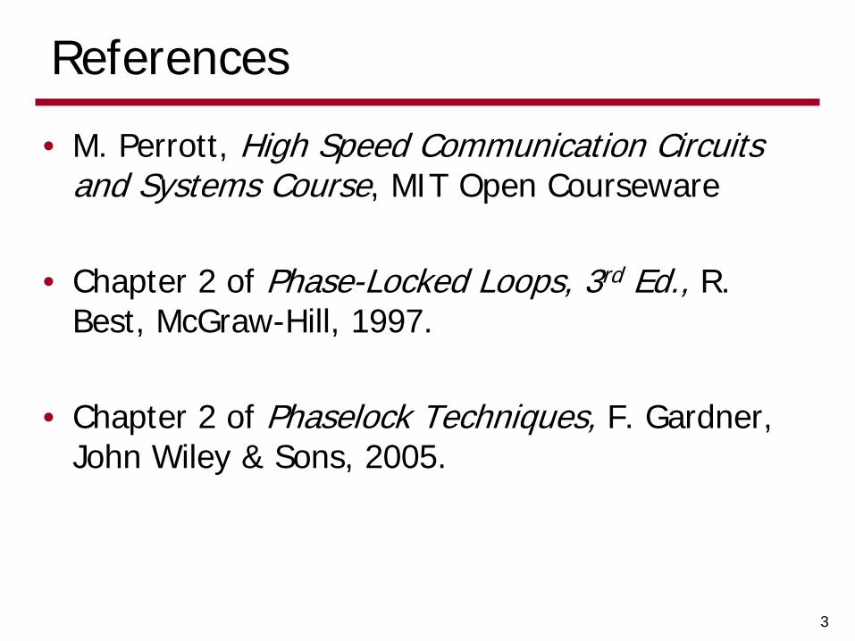
PLL Block Diagram
4
[Perrott]
• A phase-locked loop (PLL) is a negative feedback system where an oscillator-generated signal is phase AND frequency locked to a reference signal

PLL Applications
• PLLs applications • Frequency synthesis
• Multiplying a 100MHz reference clock to 10GHz
• Skew cancellation • Phase aligning an internal clock to an I/O clock
• Clock recovery • Extract from incoming data stream the clock frequency and
optimum phase of high-speed sampling clocks
• Modulation/De-modulation • Wireless systems • Spread-spectrum clocking
5

Forward Clock I/O Circuits
6
• TX PLL
• TX Clock Distribution
• Replica TX Clock Driver
• Channel
• Forward Clock Amplifier
• RX Clock Distribution
• De-Skew Circuit • DLL/PI • Injection-Locked Oscillator
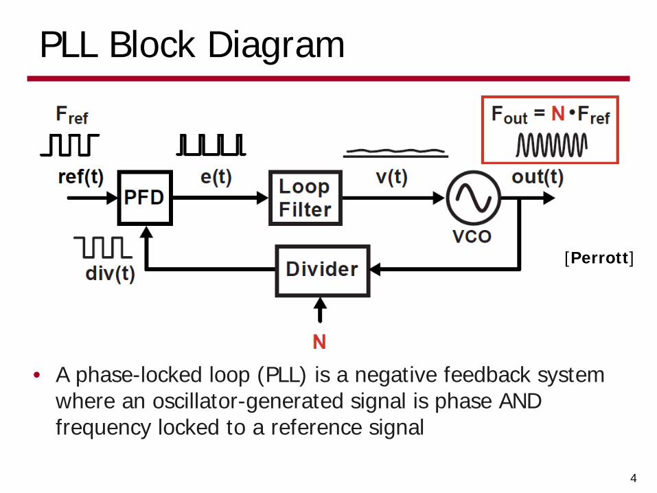
Embedded Clock I/O Circuits
7
• TX PLL
• TX Clock Distribution
• CDR • Per-channel PLL-based • Dual-loop w/ Global PLL &
• Local DLL/PI • Local Phase-Rotator PLLs • Global PLL requires RX
clock distribution to individual channels
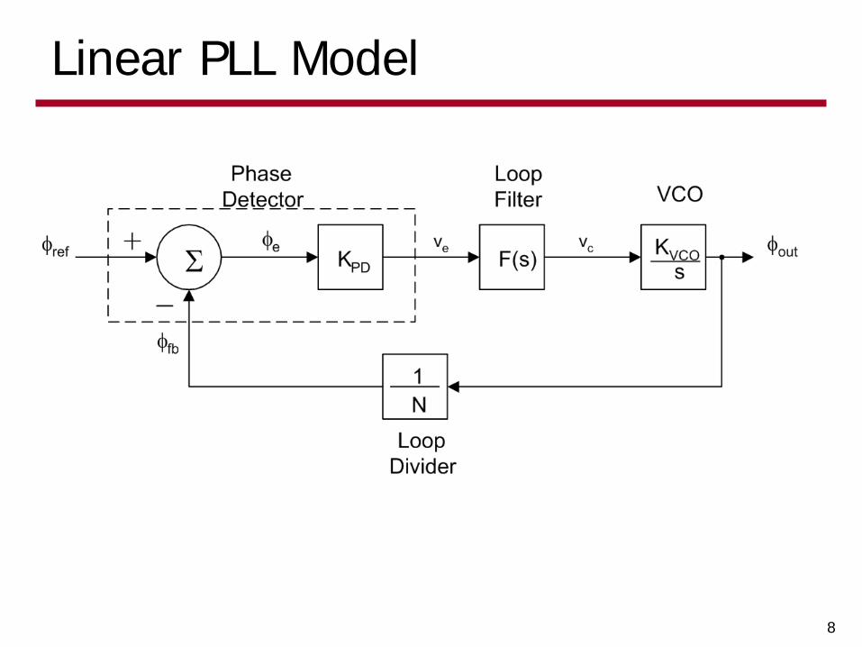
Linear PLL Model
8

Phase Detector
• Detects phase difference between feedback clock and reference clock • The loop filter will filter the phase detector output, thus to characterize
phase detector gain, extract average output voltage (or current for charge-pump PLLs)
9
φref
φfb
φe

Loop Filter
• Lowpass filter extracts average of phase detector error pulses
10
I
I
VCO ControlVoltage
C1
R
C2
Charging
Discharging
VDD
VSSF(s)

Voltage-Controlled Oscillator
• Time-domain phase relationship
11
VDDVDD/20
ω0 1KVCO
( ) ( ) ( )tvKtt cVCOoutout +=∆+= 00 ωωωω
( ) ( ) ( )∫ ∫=∆= dtdt tvKtt cVCOoutout ωφLaplace Domain Model
φout(t)
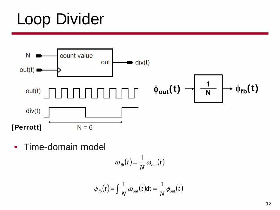
Loop Divider
• Time-domain model
12
( ) ( )tN
t outfb ωω 1=
( ) ( ) ( )∫ == tN
tN
t outoutfb φωφ 1dt1
[Perrott]
φout(t) φfb(t)

Phase & Frequency Relationships
13
• Phase Step
( ) ( )
( ) ( )∫=
=
t
o
t
tdt
ττωφ
ωφ
d
td
phase of time) vschange of (rate derivativefirst theisFrequency Angular
( ) ( ) ( )
( ) ( ) ( )( )ttu
tu
111
111
tsint
phase and tfrequency angular with t sinusoid aConsider
φω
φω
+=
( ) ( )
( ) ( ) ( )( )
frequencyin change No
sin 11
1
tuttu
tut
∆Φ+=
∆Φ=
ω
φ
∆Φ
[Best]
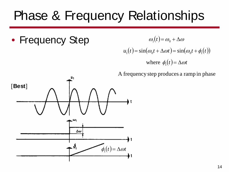
Phase & Frequency Relationships
14
• Frequency Step ( )
( ) ( ) ( )( )
( )
phasein ramp a produces stepfrequency A
where
sinsin
1
1001
01
tt
tttttu
t
ωφ
φωωω
ωωω
∆=
+=∆+=
∆+=
[Best]
( ) tt ωφ ∆=1
( )
( ) ( )( )
( )
phasein change quadratic a produces rampfrequency A
2 where
sin2
sinsin
21
102
00
01
01
tt
ttttdtu
tt
t
•
••
•
∆=
+=
∆+=
∆+=
∆+=
∫
ωφ
φωωωττωω
ωωω
Phase & Frequency Relationships
15
[Best]
• Frequency Ramp
0ω t•
∆+ ωω0
( ) 21 2
tt•
∆=
ωφ

Understanding PLL Frequency Response
• Linear “small-signal” analysis is useful for understand PLL dynamics if • PLL is locked (or near lock) • Input phase deviation amplitude is small enough to maintain operation in
lock range
• Frequency domain analysis can tell us how well the PLL tracks the input phase as it changes at a certain frequency
• PLL transfer function is different depending on which point in the loop the output is responding to
16
Input phase response VCO output response
[Fischette]

Open-Loop PLL Transfer Function
17
( ) ( )( )
( )s
sFKKsssG VCOPD
e
out =ΦΦ
=
• Open-loop response generally decreases with frequency

Closed-Loop PLL Transfer Function
18
( ) ( )( )
( )( )
( )( )
NsFKKs
sFKK
NsG
sGsssH
VCOPD
VCOPD
ref
out
+=
+=
ΦΦ
=1
( )
( ) ( )
( ) ( )N
sGN
sG
NsG
sNsFKKl
sG
VCOPD
+=+
−−=∆
=−=∆
−=−=
=
101t Determinan System
101t DeterminanPath Forward
Gain Loop
GainPath Forward
1
1
• Low-pass response whose overall order is set by F(s)

PLL Error Transfer Function
19
( ) ( )( ) ( ) ( )
NsFKKs
s
NsGs
ssEVCOPDref
e
+=
+=
ΦΦ
=1
1
( ) ( )
( ) ( )N
sGN
sG
NsG
sNsFKKl VCOPD
+=+
−−=∆
=−=∆
−=−=
=
101t Determinan System
101t DeterminanPath Forward
Gain Loop
1GainPath Forward
1
1
• Ideally, we want this to be zero • Phase error generally increases with
frequency due to this high-pass response
Next Time
• PLL System Analysis • 1st-Order PLLs • 2nd-Order PLLs
• Type 1 • Type 2
• PLL Frequency Response • Noise Transfer Functions • Tracking Response
20