ECEN620: Network Theory Broadband Circuit Design Fall...
27
Sam Palermo Analog & Mixed-Signal Center Texas A&M University ECEN620: Network Theory Broadband Circuit Design Fall 2014 Lecture 10: Voltage-Controlled Oscillators
-
Upload
vuongnguyet -
Category
Documents
-
view
220 -
download
0
Transcript of ECEN620: Network Theory Broadband Circuit Design Fall...

Sam PalermoAnalog & Mixed-Signal Center
Texas A&M University
ECEN620: Network TheoryBroadband Circuit Design
Fall 2014
Lecture 10: Voltage-Controlled Oscillators

Announcements & Agenda
• HW3 is due Friday Oct 17
• VCO Fundamentals• VCO Examples• VCO Noise
2

Charge-Pump PLL Circuits
• Phase Detector
• Charge-Pump
• Loop Filter
• VCO
• Divider
3
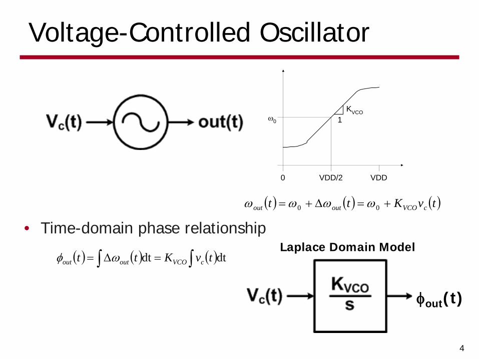
Voltage-Controlled Oscillator
• Time-domain phase relationship
VDDVDD/20
ω0 1KVCO
( ) ( ) ( )tvKtt cVCOoutout +=∆+= 00 ωωωω
( ) ( ) ( )∫ ∫=∆= dtdt tvKtt cVCOoutout ωφLaplace Domain Model
φout(t)
4

Voltage-Controlled Oscillators (VCO)
• Ring Oscillator• Easy to integrate• Wide tuning range (5x)• Higher phase noise
• LC Oscillator• Large area• Narrow tuning range (20-30%)• Lower phase noise
5
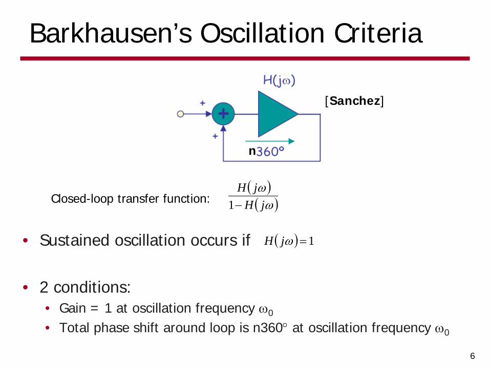
Barkhausen’s Oscillation Criteria
• Sustained oscillation occurs if
• 2 conditions:• Gain = 1 at oscillation frequency ω0
• Total phase shift around loop is n360° at oscillation frequency ω0
( )( )ωωjH
jH−1Closed-loop transfer function:
( ) 1=ωjH
n
[Sanchez]
6

Ring Oscillator Example[Sanchez]
7

Ring Oscillator Example
• 4-stage oscillator – work this one out yourself• A0 = sqrt(2)• Phase shift = 45°
• Easier to make a larger-stage oscillator oscillate, as it requires less gain and phase shift per stage, but it will oscillate at a lower frequency
M1 M1
RR
vi+
vout-
vi-
vout+
C C
8

LC Oscillator Example
( )
( ) ( ) 221
22211
221
22
12
11
1
1
1
ωωωω
CRCLLRjsZ
sCRsCLsLRsZ
S
Seq
S
Seq
+−
+==
+++
=
LC tank impedance
• Oscillation phase shift condition satisfied at the frequency when the LC (and R) tank load displays a purely real impedance, i.e. 0° phase shift

LC Oscillator Example
• Transforming the series loss resistor of the inductor to an equivalent parallel resistance
SPP
SP R
LRCCLRLL
221
1221
2
1 ,,1 ωω
≈=
+=
PPCL1
1 =ω
RP
[Razavi]
10

LC Oscillator Example
( ) 12 ≥PmRg
PPCL1
1 =ω
Loop Gain
• Phase condition satisfied at
• Gain condition satisfied when
[Razavi]
• Can also view this circuit as a parallel combination of a tank with loss resistance 2RP and negative resistance of 2/gm
• Oscillation is satisfied when
Pm
Rg
≤1
11
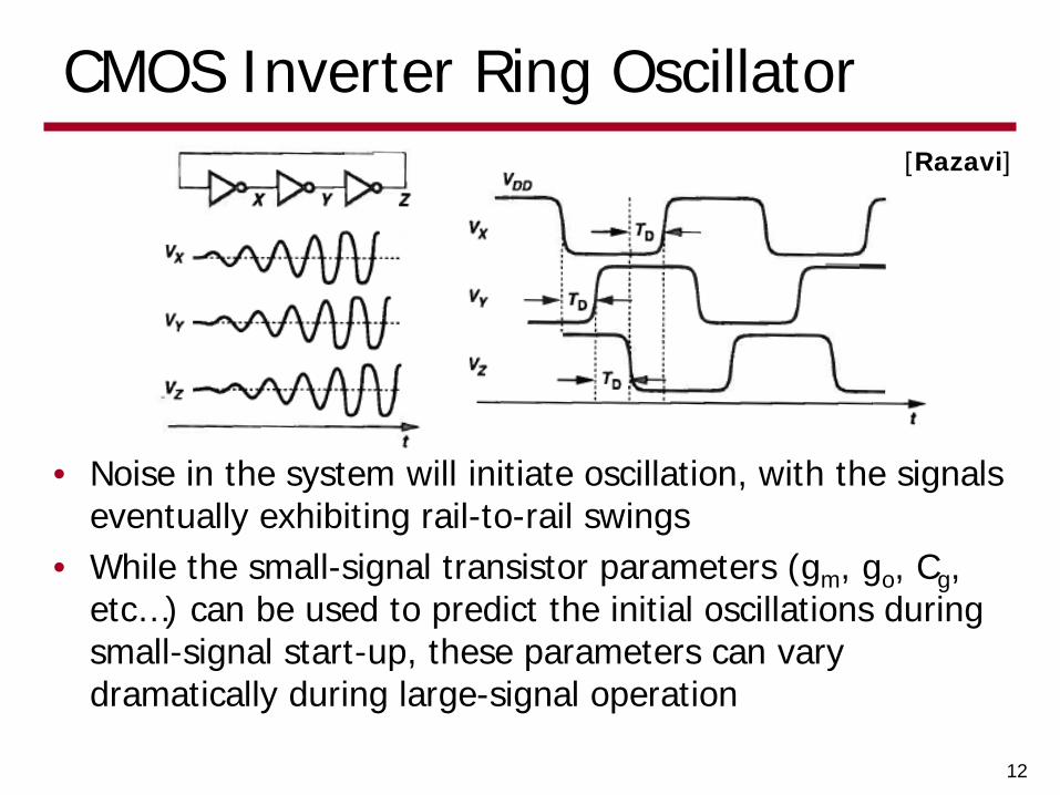
• Noise in the system will initiate oscillation, with the signals eventually exhibiting rail-to-rail swings
• While the small-signal transistor parameters (gm, go, Cg, etc…) can be used to predict the initial oscillations during small-signal start-up, these parameters can vary dramatically during large-signal operation
CMOS Inverter Ring Oscillator[Razavi]
12

• For this large-signal oscillator, the frequency is set by the stage delay, TD
• TD is a function of the nonlinear current drive and capacitances of each stage
• As an “edge” has to propagate twice around the loop
CMOS Inverter Ring Oscillator[Razavi]
number stage oscillator theis N where2
1or ,6
1DD
osc NTTf =
13

Supply-Tuned Ring Oscillator
( )thc
stageDVCO VV
nCnTT
−≈=β
22
stagec
VCOVCO nCV
fK2
β=
∂∂
=
[Sidiropoulos VLSI 2000]
14

Current-Starved Ring Oscillator
[Sanchez]
15

Capacitive-Tuned Ring Oscillator
16

Symmetric Load Ring Oscillator[Maneatis JSSC 1996 & 2003]
• Symmetric load provides frequency tuning at excellent supply noise rejection
• See Maneatis papers for self-biased techniques to obtain constant damping factor and loop bandwidth (% of ref clk)
2ID
17

LC Oscillator
• A variable capacitor (varactor) is often used to adjust oscillation frequency
• Total capacitance includes both tuning capacitance and fixed capacitances which reduce the tuning range
( )fixedtunePPPosc CCLCL +
==11ω
18

Varactors
• pn junction varactor• Avoid forward bias region to prevent oscillator nonlinearity
• MOS varactor• Accumulation-mode devices have better Q than inversion-mode
[Perrott]
n-well[Razavi]
19
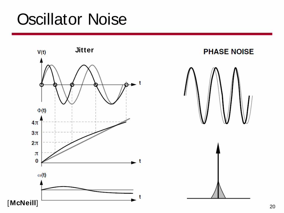
Oscillator Noise
Jitter
[McNeill] 20

Oscillator Phase Noise Model
( ) ( )dBc/Hz PowerCarrier
Density Spectral Noise
= log10fL
( )
∆
∆+
∆
+=∆f
f
ff
QPFkTfL fo
sig
3/12
12112log10Leeson’s Model:
• For improved model see Hajimiri papers
[Perrott]
21

Open-Loop VCO Jitter
• Measure distribution of clock threshold crossings• Plot σ as a function of delay ∆T
[McNeill]
∆T
22

Open-Loop VCO Jitter
• Jitter σ is proportional to sqrt(∆T)• Κ is VCO time domain figure of merit
( )( ) TTOLT ∆≈∆∆ κσ
[McNeill]
23

VCO in Closed-Loop PLL Jitter
• PLL limits σ for delays longer than loop bandwidth τL
LL fπτ 21=
[McNeill]
24

Ref Clk-Referenced vs Self-Referenced
[McNeill]
Ref Clock for Frequency Synthesis PLL
• Generally, we care about the jitter w.r.t. the ref. clock (σx)• However, may be easier to measure w.r.t. delayed version of output clk
• Due to noise on both edges, this will be increased by a sqrt(2) factor relative to the reference clock-referred jitter
CDR Example
25

Converting Phase Noise to Jitter
• Integration range depends on application bandwidth• fmin set by standard
• Ex. Assumed CDR tracking bandwidth• Usually stop integration at fo/2 or fo due to measurement limitations
and aliasing components
( ) ( )dfTffSo
T ∫∞
∆ ∆=0
22
2 sin8 πω
σ ϕ• RMS jitter for ∆T accumulation
• As ∆T goes to ∞ ( ) ( )dffSRoo
T ∫∞
==0
222 402
ϕϕ ωωσ
[Mansuri]
26

Next Time
• VCO Noise (cont.)• Divider Circuits
27


![ECEN620: Network Theory Broadband Circuit Design Fall 2019ece.tamu.edu/~spalermo/ecen620/lecture07_ee620_vcos.pdf• VCO Jitter 23. Oscillator Noise 24 Jitter [McNeill] Phase Noise](https://static.fdocuments.us/doc/165x107/5eb0f0afdb23476d411ded00/ecen620-network-theory-broadband-circuit-design-fall-spalermoecen620lecture07ee620vcospdf.jpg)