ECEN689: Special Topics in High-Speed Links Circuits and...
50
Sam Palermo Analog & Mixed-Signal Center Texas A&M University ECEN689: Special Topics in High-Speed Links Circuits and Systems Spring 2011 Lecture 19: Forwarded Clock Deskew Circuits
Transcript of ECEN689: Special Topics in High-Speed Links Circuits and...

Sam PalermoAnalog & Mixed-Signal Center
Texas A&M University
ECEN689: Special Topics in High-Speed Links Circuits and Systems
Spring 2011
Lecture 19: Forwarded Clock Deskew Circuits

Announcements
• No class on Friday• Project preliminary report #2 due on Monday in
class• Expand on report #1
• Project feedback meetings during Thursday office hours (9-10:30AM)
• Exam 2 is on Friday April 29• Comprehensive, but will focus on lectures 11 and later• 60 minutes• 1 standard 8.5x11 note sheet (front & back)• Bring your calculator
2

Agenda
• Forwarded Clock I/O Overview• Data & Clock Skew Performance Impact• Jitter Impulse Response and Jitter Transfer
Function• Forwarded Clock Deskew Architectures
• PLL/PI• DLL/PI• ILO
• Fundamental, Super-Harmonic, Sub-Harmonic
3

Forwarded Clock I/O Architecture
4
• Common high-speed reference clock is forwarded from TX chip to RX chip• Mesochronous system
• Used in processor-memory interfaces and multi-processor communication• Intel QPI• Hypertransport
• Requires one extra clock channel
• “Coherent” clocking allows low-to-high frequency jitter tracking
• Need good clock receive amplifier as the forwarded clock is attenuated by the channel

Forwarded Clock I/O Limitations
5
• Clock skew can limited forward clock I/O performance• Driver strength and loading
mismatches• Interconnect length
mismatches
• Low pass channel causes jitter amplification
• Duty-Cycle variations of forwarded clock

Forwarded Clock I/O De-Skew
6
• Per-channel de-skew allows for significant data rate increases
• Sample clock adjusted to center clock on the incoming data eye
• Implementations• Delay-Locked Loop and Phase
Interpolators• Injection-Locked Oscillators
• Phase Acquisition can be • BER based – no additional
input phase samplers• Phase detector based
implemented with additional input phase samplers periodically powered on

Forwarded Clock I/O Circuits
7
• TX PLL
• TX Clock Distribution
• Replica TX Clock Driver
• Channel
• Forward Clock Amplifier
• RX Clock Distribution
• De-Skew Circuit• PLL/PI • DLL/PI• Injection-Locked Oscillator

Data & Clock Skew Performance Impact
8
• High speed forwarded clock allows jitter tracking between clock and data
•Clock to data skew causes that high frequency clock and data jitters become out of phase on the receiver

Impact of Clock to Data Skew on Jitter Tracking
9
UI = 100psAssuming 5UI skew in this example
Jitter Frequency = 100MHz
0 0.1 0.2 0.3 0.4 0.5 0.6 0.7 0.8 0.9 1
x 10-8
-0.5
0
0.5data jitter
JD(U
I)
0 0.1 0.2 0.3 0.4 0.5 0.6 0.7 0.8 0.9 1
x 10-8
-0.5
0
0.5clock jitter
JC(U
I)
0 0.1 0.2 0.3 0.4 0.5 0.6 0.7 0.8 0.9 1
x 10-8
-0.5
0
0.5differential jitter
Jdiff
(UI)
time
skew of mUI between data and clock

Impact of Clock to Data Skew on Jitter Tracking
10
0 0.1 0.2 0.3 0.4 0.5 0.6 0.7 0.8 0.9 1
x 10-8
-0.5
0
0.5data jitter
JD(U
I)
0 0.1 0.2 0.3 0.4 0.5 0.6 0.7 0.8 0.9 1
x 10-8
-0.5
0
0.5clock jitter
JC(U
I)
0 0.1 0.2 0.3 0.4 0.5 0.6 0.7 0.8 0.9 1
x 10-8
-0.5
0
0.5differential jitter
Jdiff
(UI)
time
Jitter Frequency = 200MHz

Impact of Clock to Data Skew on Jitter Tracking
11
Jitter Frequency = 400MHz
The clock skew flips the jitter phase of clock faster for higher frequency jitter and results in higher differential jitter
0 0.1 0.2 0.3 0.4 0.5 0.6 0.7 0.8 0.9 1
x 10-8
-0.5
0
0.5data jitter
JD(U
I)
0 0.1 0.2 0.3 0.4 0.5 0.6 0.7 0.8 0.9 1
x 10-8
-0.5
0
0.5clock jitter
JC(U
I)
0 0.1 0.2 0.3 0.4 0.5 0.6 0.7 0.8 0.9 1
x 10-8
-0.5
0
0.5differential jitter
Jdiff
(UI)
time

Impact of Clock to Data Skew on Jitter Tracking
•
12
[1] Ganesh Balamurugan et al., “Modeling and mitigation of jitter in high-speed source-synchronous interchip communication systems,” Conference Record of the Thirty-Seventh Asilomar Conference on Signals, Systems and Computers, vol. 2, no. 2, pp. 1681-1687, Nov. 2003.
0 1 2 3 4 5 6 7 8 9 10
x 108
0
0.5
1
1.5
2
2.5
3
3.5
4
Jitter Frequency(Hz)
Nor
mal
ized
Diff
eren
tial J
itter
1UI
2UI
3UI
4UI5UI
Larger clock to data skew increases differential jitter at lower jitter frequencies

Optimum Jitter Tracking for 200MHz jitter
•
13
Controllable JTB over 70 - 800MHz is desired
In 10Gb/s system,UI = 100ps
Jitter Frequency = 200MHz

Jitter Impulse Response(JIR) and Jitter Transfer Function(JTF) Analysis Method
14
• JIR: test the system response on jitter• JTF: ratio of output to input jitter as a function of frequency,
DTFT of JIR
B. Casper and F. O’Mahony, “Clocking analysis, implementation and measurement techniques for high-speed data links a tutorial,” IEEE Trans. Circuits Syst. I, vol. 56, no. 1, pp. 683–688, Jan. 2009.
Ideal clock waveform superimposed with clock incorporating jitter impulse stimulus
Output clock waveforms using ideal clock versus jitter impulse clock
Jitter impulse response
Extraction of JIR in ½ rate system where both clock edges are using
• A clock system’s effect on an input jitter sequence can be evaluatedby convolving the jitter sequence with the jitter impulse response

Filter/Amplifier Frequency Response & Jitter Transfer Response
15
• Low-pass frequency response (buffer, distribution interconnect) is similar to a high-pass jitter filter• High frequency jitter is
amplified
• High-pass frequency response (AC coupling cap) is similar to an all-pass jitter filter, except for Nyquist-rate jitter (duty cycle error)
• Band-pass frequency response (band-pass filter) is similar to a low-pass jitter filter with the center frequency aligned with the fundamental clock frequency
B. Casper and F. O’Mahony, “Clocking analysis, implementation and measurement techniques for high-speed data links a tutorial,” IEEE Trans. Circuits Syst. I, vol. 56, no. 1, pp. 683–688, Jan. 2009.

Jitter Amplification
• Low-pass frequency response (buffer, distribution interconnect) is similar to a high-pass jitter filter• High frequency jitter is amplified as it propagates
across the channel
16
0 2 4 6 8 10 12 14-60
-50
-40
-30
-20
-10
0
Frequency (GHz)
S 21 (d
B)
0 1 2 3 4 5x 10⁹
0.5
1
1.5
2
2.5
3
Frequency(Hz)
Jitte
r Am
plifi
catio
n Fa
ctor
Channel ResponseJitter Transfer/Amplification

PLL or DLL/PI Forwarded Clock Deskew
• TX clock is forwarded along an independent channel to the RX chip where it is distributed to the RX channels
17
• The PLL or DLL locks onto the forwarded clock and serves as a multi-phase generator and a jitter filter
• The PI mixes the phases to produce sampling clocks at the optimal phase for maximum timing margin or BER
B. Casper and F. O’Mahony, “Clocking analysis, implementation and measurement techniques for high-speed data links a tutorial,” IEEE Trans. Circuits Syst. I, vol. 56, no. 1, pp. 683–688, Jan. 2009.
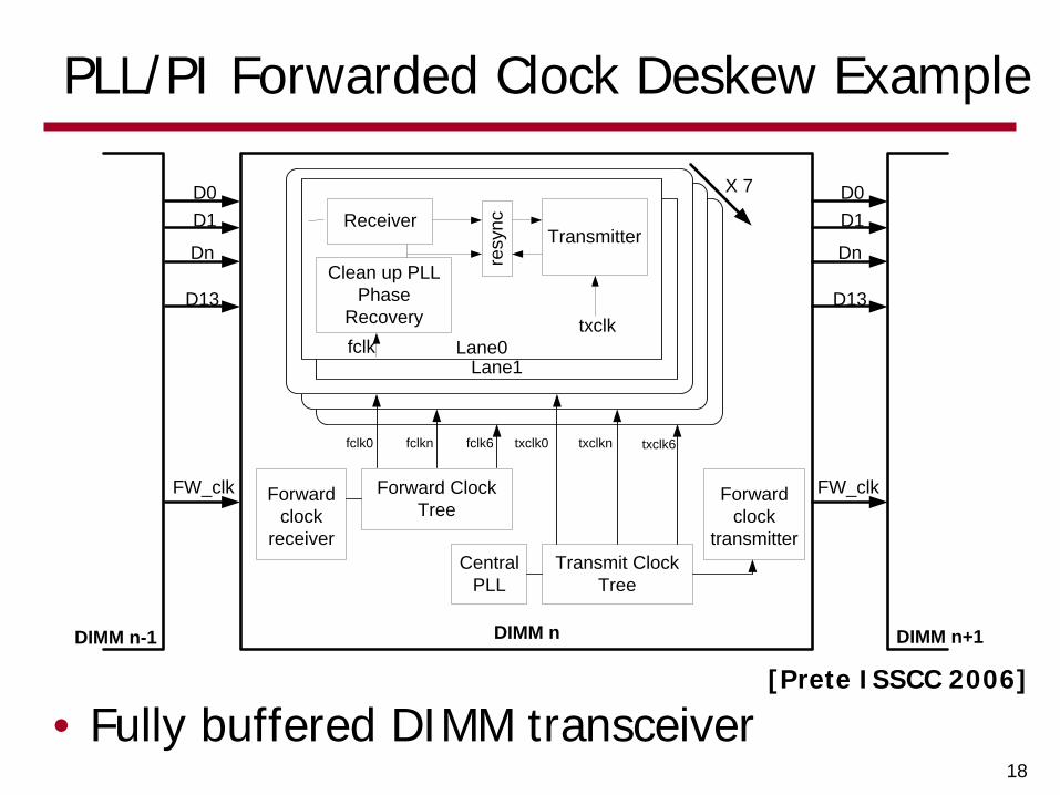
PLL/PI Forwarded Clock Deskew Example
18
DIMM n
Forwardclock
receiver
Lane1Lane0
Receiver
resy
nc Transmitter
Forward ClockTree
fclk0 fclkn fclk6
CentralPLL
Transmit ClockTree
txclk0 txclkn txclk6
Forwardclock
transmitter
DIMM n-1 DIMM n+1
D0D1
Dn
D13
FW_clk
D0D1
Dn
D13
FW_clk
Clean up PLLPhase
Recoveryfclk
txclk
X 7
• Fully buffered DIMM transceiver[Prete ISSCC 2006]

PLL/PI Forwarded Clock Deskew Example
19
• PLL low-pass jitter transfer characteristic filters high frequency jitter• Desired for uncorrelated jitter• Not desired for correlated high frequency jitter
[Prete ISSCC 2006]
VCO LoopFilter
0/18090/270
DataSamplers
45/225135/315
Phase recoverycontroller
+
ph_cnt<63:0>
data even/odd
edges even/odd
fw_clockPhase detector
mixing
Phase recovery loop (BW ~ 500KHz)
Phase Locked loop (BW > 150MHz)
+
data_in
• PLL disadvantages• Jitter accumulation in
VCO• Stability• More area and
complex than DLL implementations

DLL/PI Forwarded Clock Deskew Example
20
• DLL advantages• No jitter accumulation• Inherently stable• Simpler and less area
than PLL
• Finite bandwidth of DLL delay line can result in jitter amplification
• DLL displays an all-pass jitter transfer function• Desired for correlated jitter• Not desired for uncorrelated jitter
[Balamurugan JSSC 2008]

Injection Locking in LC Tanks
21
a) a free-running oscillator consisting of an idealpositive feedback amplifier and an LC tank;
b) we insert a phase shift in the loop. We know this will cause the oscillation frequency to shift since the loop gain has tohave exactly 2π phase shift(or multiples).

22
Phase Shift for Injected Signal
• Assume the oscillator “locks” onto the injectedcurrent and oscillates at the same frequency.
• Since the locking signal is not in general at the resonant center frequency, the tank introduces a phase shift
• In order for the oscillator loop gain to be equalto unity with zero phase shift, the sum of thecurrent of the transistor and the injectedcurrents must have the proper phase shift tocompensate for the tank phase shift.

Injection Locked Oscillator Phasors
23
Note that the frequency of the injection signal determines the extra phase shift Φ0 of the tank. This is fixed by the frequency offset.
The current from the transistor is fed by the tank voltage, which by definition the tank current times the tank impedance, which introduces Φ0 between the tank current/voltage. The angle between the injected current and the oscillator current θ must be such that their sum aligns with the tank current.

Injection Geometry
24
The geometry of the problem implies the following constraints on the injected current amplitude relative to the oscillation amplitude.

Locking Range
25
At the edge of the lock range, the injected current is orthogonal to the tank current.
The phase angle between the injected current and the oscillator is 90° + Φ0,max
iosc
inj
iosc
inj
injoscinjosc
inj
T
inj
II
ifII
IIII
III
−==⇒
++==
θφ
θ
θθφ
cos.,sin
cos2
sinsinsin
max,0
220
220
00
0
11100
220
220
201
0
,tan
)(2tan
)(tan)(tan2
,1),(2
)(tan2
injoscTT
inj
p
p
IIIII
Q
xxQR
LR
L
−==
−≈∴
=−=⋅
−≈−
−⋅
⋅−=
−−−
−
φ
ωωω
φ
πωωωωωω
ωωωωπφ
A second-order parallel tank consisting of L. C, Rp exhibits a phase shift of:
Source: Razavi

Locking Range
26
2
2
00
00
2
2
2
2
00
1
12
)(2
1
1
1
1
)(2
osc
injosc
injinj
osc
injosc
inj
osc
injosc
inj
T
osc
osc
inj
T
inj
III
IQ
Q
III
IIII
III
II
QII
−
⋅⋅≈−⇒
−≈
−
⋅⇒
−
⋅=⋅
−≈⇒
ωωω
ωωω
ωωω
osc
injinjL I
IQ⋅≈−=∆ 2
00,
ωωωω
oscinj II <<
1.0,5,10: 0 ====osc
inj
II
KQGHzWhen ω
MHzL 100, ≈=> ∆ω
Locking range is inversely proportional to oscillator Q

Digital Controlled Oscillator (DCO) with Injection Locking
27
The digitally controlled switch-capacitor bank tunes the free-running frequency of DCO to adjust the phase of the forwarded clock and also compensate for PVT.
Shekhar, Sudip et al, “Strong Injection Locking in Low-Q LC Oscillators: Modeling and Application in a Forwarded-Clocked I/O Receiver”, IEEE JSSC, 2009.
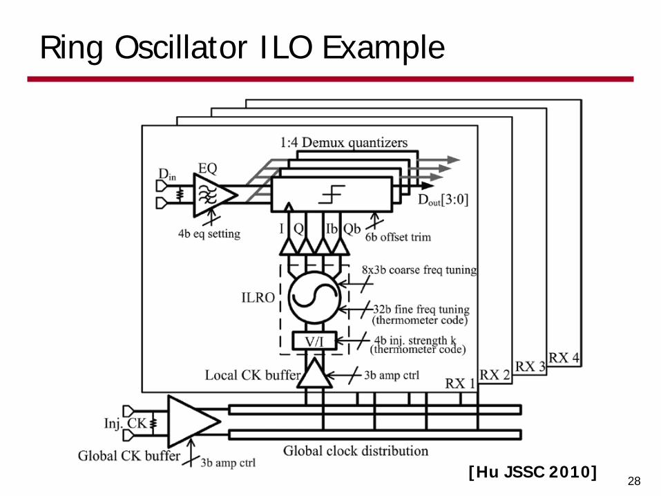
Ring Oscillator ILO Example
28[Hu JSSC 2010]

Ring Oscillator ILO Example
29[Hu JSSC 2010]

ILO Jitter Transfer
• ILOs have a first-order low-pass filter function to input (injection clock) jitter
• ILOs have a first-order high-pass filter function to VCO jitter
30
P
PVCO s
s
JTF
ω
ω
+=
1
∆≈∆
=
∆−=
− ωθω
ω
ωωω
KA
QA
AK
o
1ss
22
2
PP
sin :phase skew-de desired theoffunction a is
2 :ankresonant t RLC parallel aFor
:bandwidth ckingjitter tra theis where
P
INPUT sJTF
ω+
=1
1

ILO Jitter Transfer
• ILO jitter transfer bandwidth decreases as the oscillator is locked further from the free-running frequency, ωo, to obtain a larger phase shift θss
31
P
INPUT sJTF
ω+
=1
1
∆≈
∆−=
− ωθ
ωω
KA
AK
1ss
22
2
P
sin
[Hossain JSSC 2009]

ILO Jitter Transfer
• ILO jitter transfer bandwidth increases with injection strength
32
P
INPUT sJTF
ω+
=1
1
∆≈
∆−=
− ωθ
ωω
KA
AK
1ss
22
2
P
sin
[Hossain JSSC 2009]

ILO Jitter Transfer
• ILO jitter transfer bandwidth increases with injection strength
33
P
INPUT sJTF
ω+
=1
1
∆≈
∆−=
− ωθ
ωω
KA
AK
1ss
22
2
P
sin
[Hossain JSSC 2009]

ILO Phase Noise Filtering
• Up to jitter tracking bandwidth, ILO output phase noise is dominated by injection clock• Can be better than VCO• JTB depends on desired
de-skew phase
• At high frequencies, VCO phase noise dominates
34
( )22
2
222
22
22
22
cos
cos
ωθ
ωθ
ωωωω
ω+
+
=+
+=
+=
ss
VCOinjss
P
VCOinjPjitterout
VCOVCOinjinputout
AK
SSAK
SSS
SJTFSJTFS
[Hossain JSSC 2009]

Ring Oscillator Super-Harmonic ILO Example
35
0.5m Here == injosc mff
• Potential system application• ½ rate TX forwards clock to
¼ rate RX
[Hossain JSSC 2009]

Super-Harmonic ILO Phase Noise Filtering
36
0.5m Here == injosc mff
( )22
2
222
2
cos
cos
ωθ
ωθω
+
+
=
ss
VCOinjss
jitterout
mAK
SSmAKm
S
[Hossain JSSC 2009]
• Low frequency phase noise is actually better than injection oscillator by m2

Ring Oscillator Sub-Harmonic ILOExample w/ Clock Signal Injection
• Forwarding a lower speed clock avoids jitter amplification over low-pass channel
37
• Sub-Harmonic injection with clock signal can cause significant ILO amplitude variations and sub-harmonic spurious tones
[Hossain ISSCC 2010]

Ring Oscillator Sub-Harmonic ILOExample w/ Pulse Train Signal Injection
• Forwarding a pulse train signal reduces amplitude variations and ILO spurious tones
38
• Adjusting pulse width, d, changeseffective injection strength and can be used to adjust jitter tracking bandwidth
[Hossain ISSCC 2010]

Effective Injection Strength of Pulse Train
• Wider pulse separation (lower frequency sub-harmonics) reduces effective injection strength
39
[Hossain ISSCC 2010]

Adjusting Jitter Tracking Bandwidth w/ Pulse Train Signal
40
• Wider pulse separation (lower frequency sub-harmonics) reduces effective injection strength and results in lower jitter tracking bandwidth
• Reducing pulse width, d, for a given spacing reduces effective injection strength and results in lower jitter tracking bandwidth
[Hossain ISSCC 2010]

Optimum Jitter Tracking for 200MHz jitter
•
41
Controllable JTB over 70 - 800MHz is desired
In 10Gb/s system,UI = 100ps
Jitter Frequency = 200MHz
Objective: Implement optimal JTB that yields minimum differential jitter

Understanding of Jitter Reduction using Bandpass Filtering
•
42
fcfL fH f fcfL fH f

•
43
Understanding of Jitter Reduction using Bandpass Filtering

•
44
Understanding of Jitter Reduction using Bandpass Filtering

Analysis of Bandpass Jitter Filtering Based on JIR and JTF
45
• Transmitted jitter exhibits low-pass transfer characteristic through band-pass channel
• Received high frequency uncorrelated jitter can be reduced by a bandpass filter
15 20 25 30 35 40-2
0
2
4
6
8
x 10-12 Jitter Impluse Reponse of Bandpass System
Clocking Cycle#
Nor
mal
ized
Jitt
er
0 0.5 1 1.5 2 2.5
x 109
-25
-20
-15
-10
-5
0Jitter Transfer of Bandpass System
Freq(Hz)
Jitte
r Am
plifi
catio
n Fa
ctor

Optimum Jitter Tracking with BandpassFiltering
• Higher Q of bandpass filtering, smaller bandwidth, higher jitter filtering
46
fcfL fH
Q1
Q2
Q3
Q1 < Q2 < Q3
f

Optimum Jitter Tracking with BandpassFiltering
• Apply JIR and JTF analysis to quantify the impact of Q on JTB of 5GHz clock, UI = 100ps
47
Q tuning range over 3 -30 provides JTB range over 97 – 790 MHz
To achieve JTB of 70MHz to optimize jitter tracking with 10UI clock skew, higher Q is required.
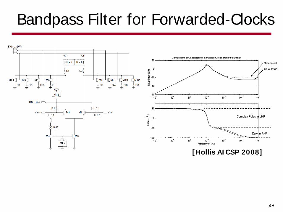
Bandpass Filter for Forwarded-Clocks
48
[Hollis AICSP 2008]

Bandpass Filter Jitter Filtering
• Bandpass filter is effective in filtering high-frequency jitter
• Low-maximum Q of the filter (Q=2.6) limits tuning to low-frequency jitter tracking bandwidths• Limited by the passive inductor Q
49

Next Time
• Clock Distribution Techniques
50