ECEN689: Special Topics in High-Speed Links Circuits and...
50
Sam Palermo Analog & Mixed-Signal Center Texas A&M University ECEN689: Special Topics in High-Speed Links Circuits and Systems Spring 2012 Lecture 12: CDRs
Transcript of ECEN689: Special Topics in High-Speed Links Circuits and...
Sam Palermo Analog & Mixed-Signal Center
Texas A&M University
ECEN689: Special Topics in High-Speed Links Circuits and Systems
Spring 2012
Lecture 12: CDRs
Announcements
• Project preliminary report #1 due now
• Stateye solution • 32-b Matlab will be installed in lab by Friday • For quicker individual solutions see Younghoon
• CDR Papers posted on website
2
Agenda
• CDR overview • CDR phase detectors • Analog & digital CDRs • Dual-loop CDRs • CDR circuits
• Phase interpolators • Delay-locked loops
• CDR jitter properties
3

Embedded Clock I/O Circuits
4
• TX PLL
• TX Clock Distribution
• CDR • Per-channel PLL-based • Dual-loop w/ Global PLL &
• Local DLL/PI • Local Phase-Rotator PLLs • Global PLL requires RX
clock distribution to individual channels
5
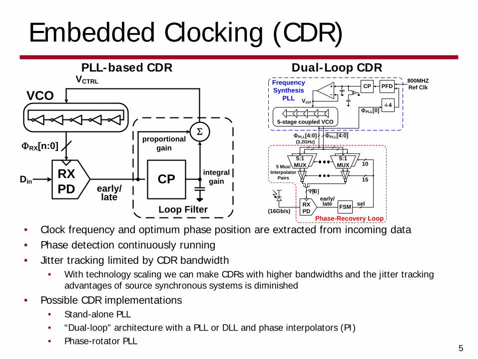
Embedded Clocking (CDR)
early/late
RXPD
CP
Σ
VCTRL
integral gain
proportional gain
VCO
Din
Loop Filter
ΦRX[n:0]
FSM selearly/late
Phase-Recovery Loop
RXPD
Ψ[4:0]
CP
Vctrl
FrequencySynthesis
PLL
5-stage coupled VCO
4
800MHZ Ref ClkPFD
ΦPLL[4:0]
(16Gb/s)
5 Mux/Interpolator
Pairs
5:1 MUX
5:1 MUX
ΦPLL[4:0](3.2GHz)
ΦPLL[0]
15
10
PLL-based CDR Dual-Loop CDR
• Clock frequency and optimum phase position are extracted from incoming data • Phase detection continuously running • Jitter tracking limited by CDR bandwidth
• With technology scaling we can make CDRs with higher bandwidths and the jitter tracking advantages of source synchronous systems is diminished
• Possible CDR implementations • Stand-alone PLL • “Dual-loop” architecture with a PLL or DLL and phase interpolators (PI) • Phase-rotator PLL
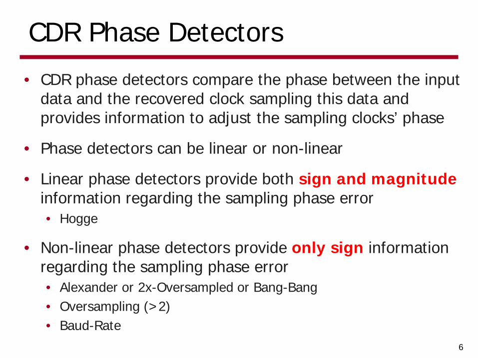
CDR Phase Detectors
• CDR phase detectors compare the phase between the input data and the recovered clock sampling this data and provides information to adjust the sampling clocks’ phase
• Phase detectors can be linear or non-linear
• Linear phase detectors provide both sign and magnitude information regarding the sampling phase error • Hogge
• Non-linear phase detectors provide only sign information regarding the sampling phase error • Alexander or 2x-Oversampled or Bang-Bang • Oversampling (>2) • Baud-Rate
6
Late
Tb/2 ref
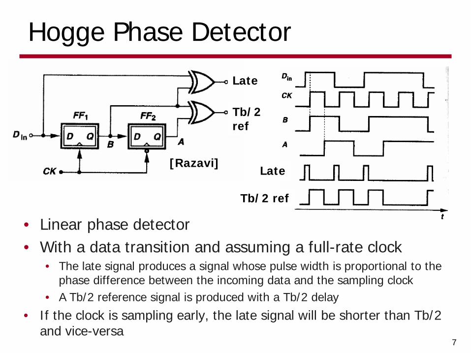
Hogge Phase Detector
• Linear phase detector • With a data transition and assuming a full-rate clock
• The late signal produces a signal whose pulse width is proportional to the phase difference between the incoming data and the sampling clock
• A Tb/2 reference signal is produced with a Tb/2 delay
• If the clock is sampling early, the late signal will be shorter than Tb/2 and vice-versa
7
Late
Tb/2 ref
[Razavi]
Late
Tb/2 ref
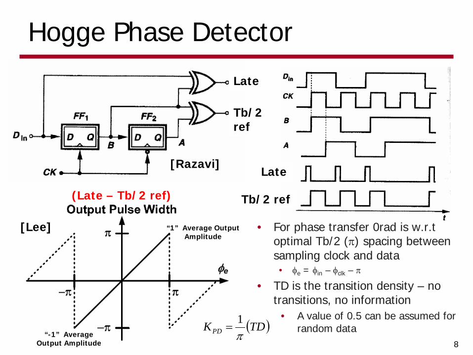
Hogge Phase Detector
• For phase transfer 0rad is w.r.t optimal Tb/2 (π) spacing between sampling clock and data
• φe = φin – φclk – π
• TD is the transition density – no transitions, no information
• A value of 0.5 can be assumed for random data
8
Late
Tb/2 ref (Late – Tb/2 ref)
“1” Average Output Amplitude
“-1” Average Output Amplitude
( )TDKPD π1
=
[Razavi]
[Lee]

Hogge Phase Detector Nonidealities
• Flip-Flop Clk-to-Q delay widens Late pulse, but doesn’t impact Tb/2 reference pulse
• CDR will lock with a phase shift to equalize Tb/2 reference and Late pulse widths
9
Late
Early
Late [Razavi]
Tb/2 ref
Hogge Phase Detector Nonidealities
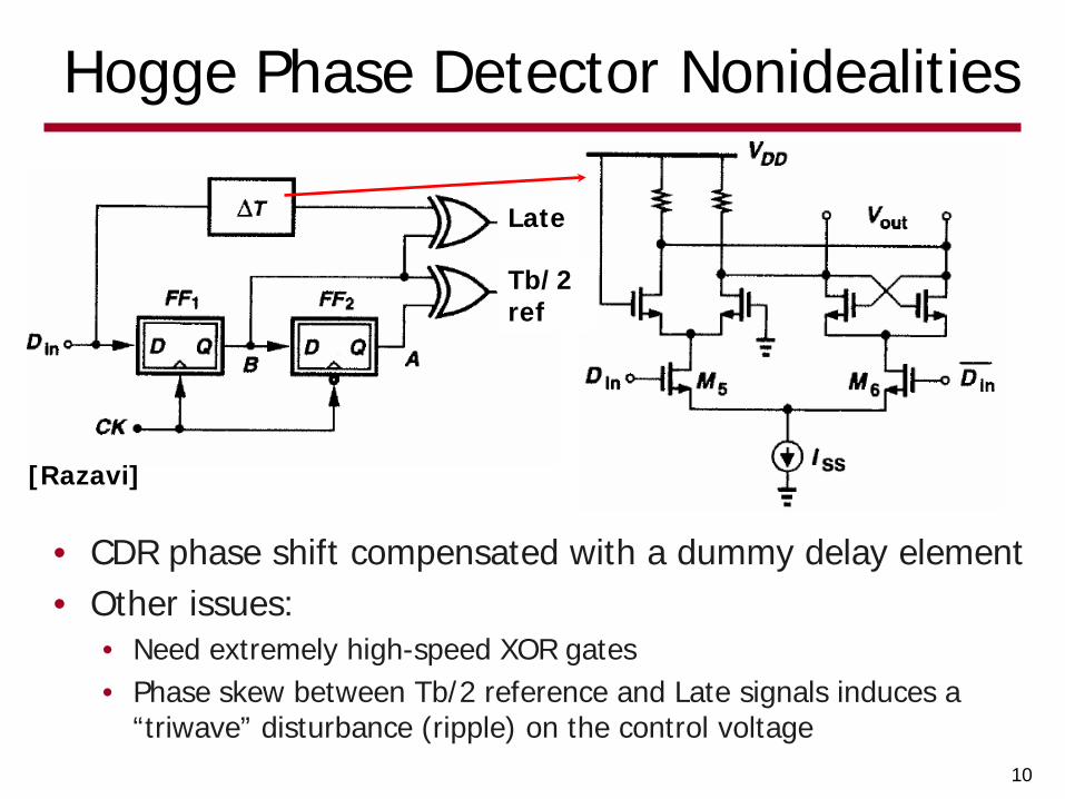
• CDR phase shift compensated with a dummy delay element • Other issues:
• Need extremely high-speed XOR gates • Phase skew between Tb/2 reference and Late signals induces a
“triwave” disturbance (ripple) on the control voltage 10
Late
Early
[Razavi]
Tb/2 ref
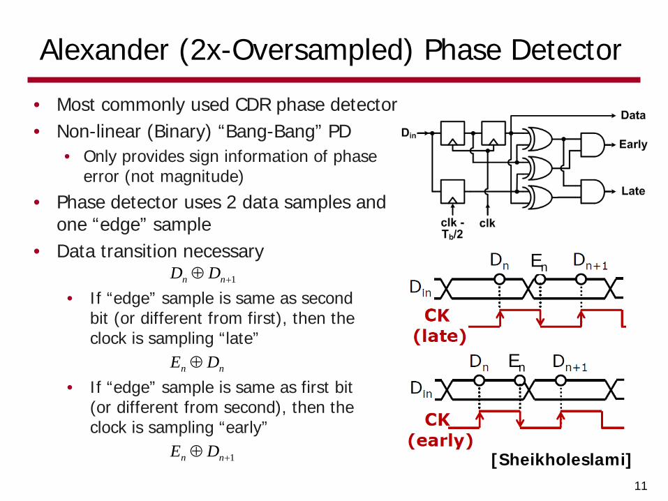
Alexander (2x-Oversampled) Phase Detector
• Most commonly used CDR phase detector • Non-linear (Binary) “Bang-Bang” PD
• Only provides sign information of phase error (not magnitude)
• Phase detector uses 2 data samples and one “edge” sample
• Data transition necessary
11
1+⊕ nn DD• If “edge” sample is same as second
bit (or different from first), then the clock is sampling “late”
nn DE ⊕• If “edge” sample is same as first bit
(or different from second), then the clock is sampling “early”
1+⊕ nn DE
En
En
[Sheikholeslami]
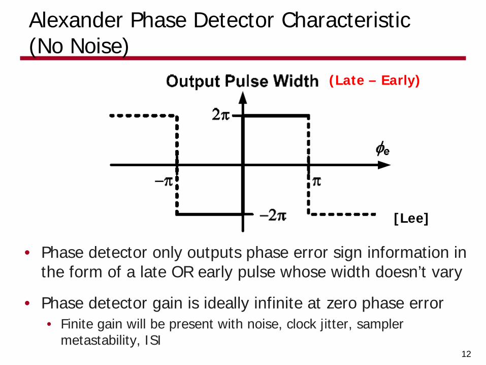
Alexander Phase Detector Characteristic (No Noise)
• Phase detector only outputs phase error sign information in the form of a late OR early pulse whose width doesn’t vary
• Phase detector gain is ideally infinite at zero phase error • Finite gain will be present with noise, clock jitter, sampler
metastability, ISI 12
(Late – Early)
[Lee]
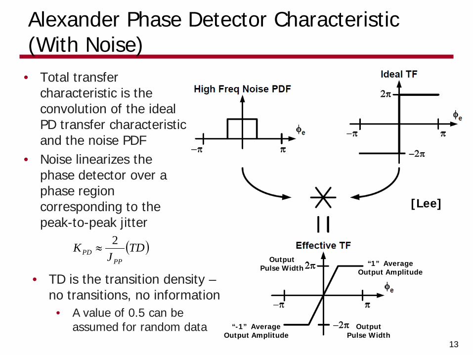
Alexander Phase Detector Characteristic (With Noise)
• Total transfer characteristic is the convolution of the ideal PD transfer characteristic and the noise PDF
• Noise linearizes the phase detector over a phase region corresponding to the peak-to-peak jitter
13
[Lee]
( )TDJ
KPP
PD2
≈
• TD is the transition density – no transitions, no information • A value of 0.5 can be
assumed for random data
Output Pulse Width
Output Pulse Width
“1” Average Output Amplitude
“-1” Average Output Amplitude
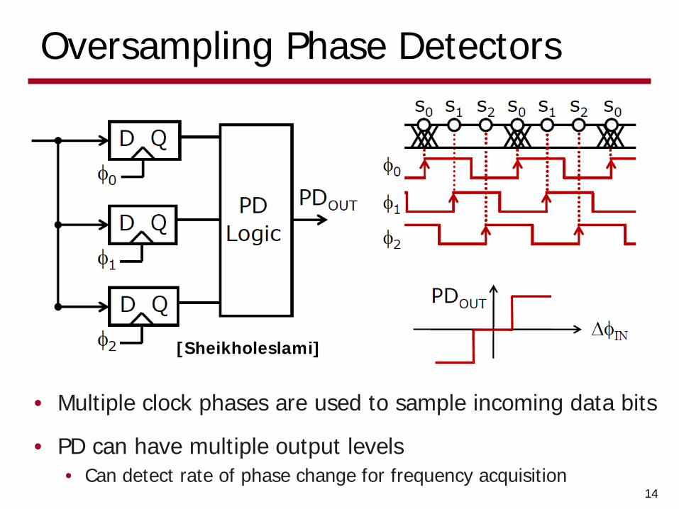
Oversampling Phase Detectors
• Multiple clock phases are used to sample incoming data bits
• PD can have multiple output levels • Can detect rate of phase change for frequency acquisition
14
[Sheikholeslami]
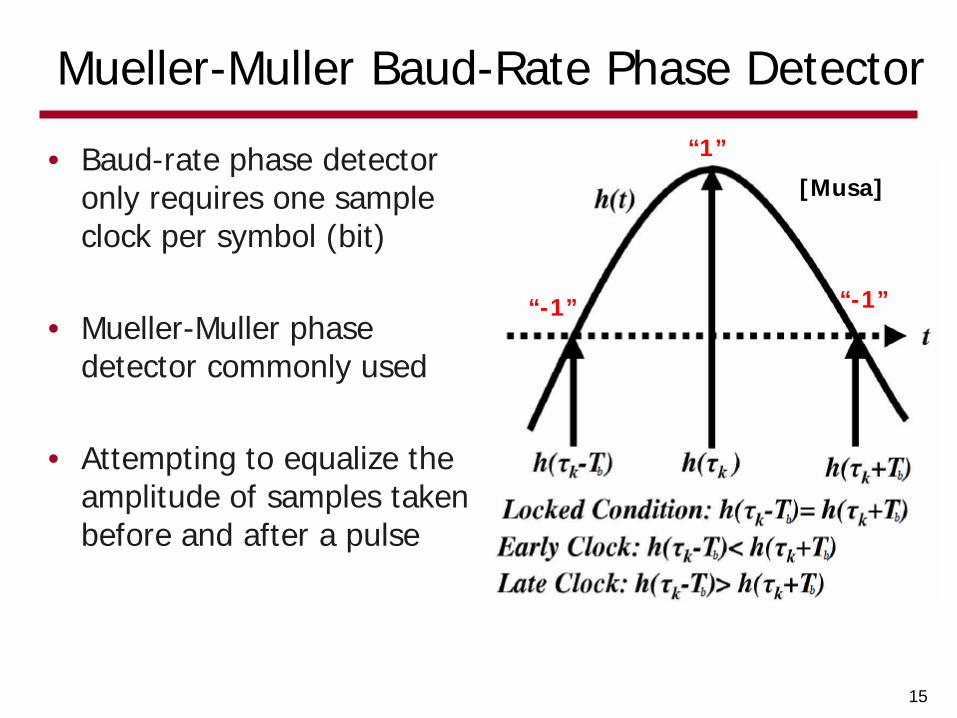
Mueller-Muller Baud-Rate Phase Detector
• Baud-rate phase detector only requires one sample clock per symbol (bit)
• Mueller-Muller phase detector commonly used
• Attempting to equalize the amplitude of samples taken before and after a pulse
15
“-1”
“1”
“-1”
[Musa]

Mueller-Muller Baud-Rate Phase Detector
16
[Spagna ISSCC 2010]
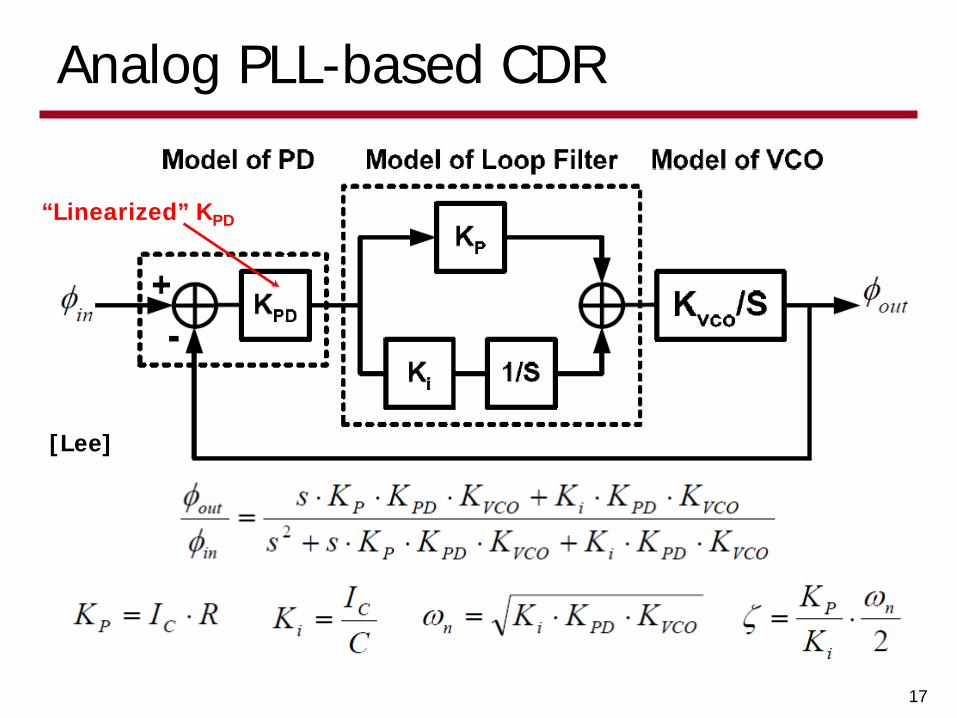
Analog PLL-based CDR
17
“Linearized” KPD
[Lee]

Analog PLL-based CDR
18
• CDR “bandwidth” will vary with input phase variation amplitude with a non-linear phase detector
• Final performance verification should be done with a time-domain non-linear model
[Lee]
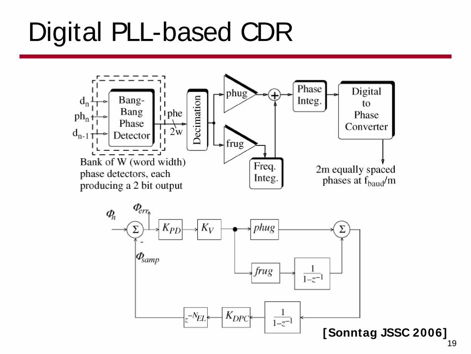
Digital PLL-based CDR
19 [Sonntag JSSC 2006]

Digital PLL-based CDR
20
Open-Loop Gain:
[Sonntag JSSC 2006]

Digital PLL-based CDR
21 [Sonntag JSSC 2006]

Single-Loop CDR Issues
• Phase detectors have limited frequency acquisition range • Results in long lock times or not locking at all • Can potentially lock to harmonics of correct clock frequency
• VCO frequency range variation with process, voltage, and temperature can exceed PLL lock range if only a phase detector is employed
22
early/late
RXPD
CP
Σ
VCTRL
integral gain
proportional gain
VCO
Din
Loop Filter
ΦRX[n:0]
PLL-based CDR
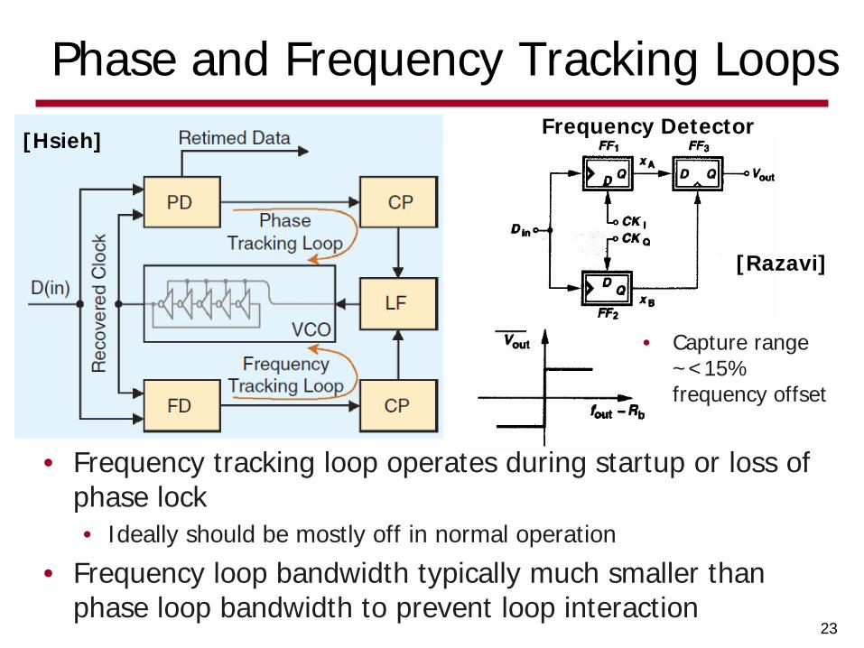
Phase and Frequency Tracking Loops
• Frequency tracking loop operates during startup or loss of phase lock • Ideally should be mostly off in normal operation
• Frequency loop bandwidth typically much smaller than phase loop bandwidth to prevent loop interaction
23
Frequency Detector
• Capture range ~<15% frequency offset
[Hsieh]
[Razavi]

Analog Dual-Loop CDR w/ Two VCOs
• Frequency synthesis loop with replica VCO provides a “coarse” control voltage to set phase tracking loop frequency
• Frequency loop can be a global PLL shared by multiple channels
• Issues • VCO matching • VCO pulling • Distributing voltage long
distances 24
[Hsieh]
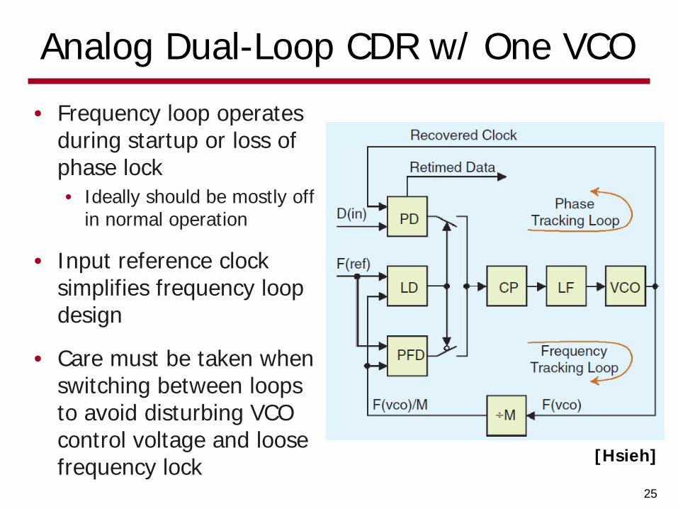
Analog Dual-Loop CDR w/ One VCO
• Frequency loop operates during startup or loss of phase lock • Ideally should be mostly off
in normal operation
• Input reference clock simplifies frequency loop design
• Care must be taken when switching between loops to avoid disturbing VCO control voltage and loose frequency lock
25
[Hsieh]

Phase Interpolator (PI) Based CDR • Frequency synthesis loop
produces multiple clock phases used by the phase interpolators
• Phase interpolator mixes between input phases to produce a fine sampling phase • Ex: Quadrature 90° PI inputs
with 5 bit resolution provides sampling phases spaced by 90°/(25-1)=2.9°
• Digital phase tracking loop offers advantages in robustness, area, and flexibility to easily reprogram loop parameters
26
[Hsieh]

Phase Interpolator (PI) Based CDR
• Frequency synthesis loop can be a global PLL
• Can be difficult to distribute multiple phases long distance • Need to preserve phase
spacing • Clock distribution power
increases with phase number • If CDR needs more than 4
phases consider local phase generation
27

DLL Local Phase Generation
• Only differential clock is distributed from global PLL
• Delay-Locked Loop (DLL) locally generates the multiple clock phases for the phase interpolators • DLL can be per-channel or
shared by a small number (4)
• Same architecture can be used in a forwarded-clock system • Replace frequency synthesis
PLL with forwarded-clock signals
28
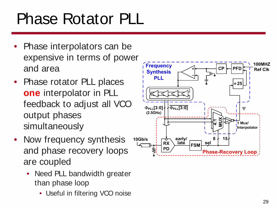
Phase Rotator PLL
• Phase interpolators can be expensive in terms of power and area
• Phase rotator PLL places one interpolator in PLL feedback to adjust all VCO output phases simultaneously
• Now frequency synthesis and phase recovery loops are coupled • Need PLL bandwidth greater
than phase loop • Useful in filtering VCO noise
29
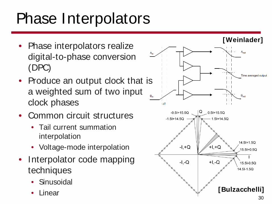
Phase Interpolators
• Phase interpolators realize digital-to-phase conversion (DPC)
• Produce an output clock that is a weighted sum of two input clock phases
• Common circuit structures • Tail current summation
interpolation • Voltage-mode interpolation
• Interpolator code mapping techniques • Sinusoidal • Linear
30
[Bulzacchelli]
[Weinlader]
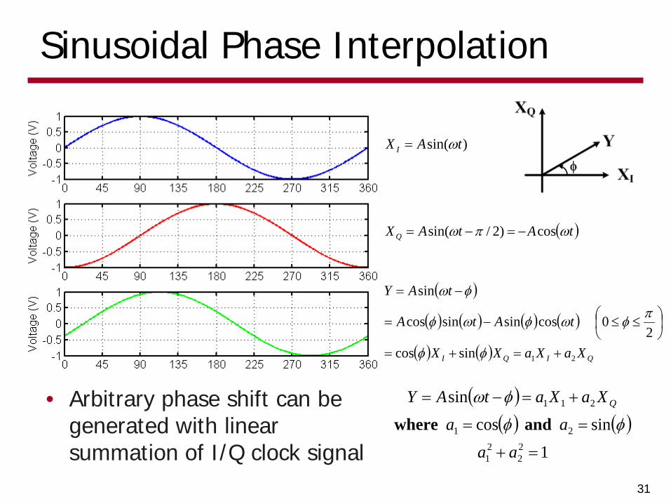
Sinusoidal Phase Interpolation
31
)sin( tAX I ω=
( )tAtAX Q ωπω cos)2/sin( −=−=
( )
( ) ( ) ( ) ( )
( ) ( ) QIQI XaXaXX
tAtA
tAY
21sincos2
0cossinsincos
sin
+=+=
≤≤−=
−=
φφ
πφωφωφ
φω
• Arbitrary phase shift can be generated with linear summation of I/Q clock signal
( )( ) ( )
1
sincos
sin
22
21
21
211
=+
==
+=−=
aaaa
XaXatAY Q
φφ
φω
and where
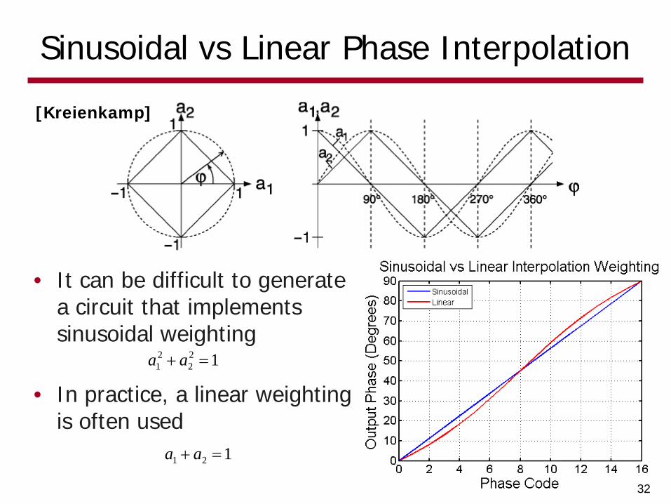
Sinusoidal vs Linear Phase Interpolation
32
• It can be difficult to generate a circuit that implements sinusoidal weighting
122
21 =+ aa
• In practice, a linear weighting is often used
121 =+ aa
[Kreienkamp]
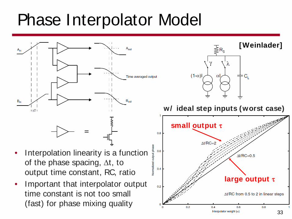
Phase Interpolator Model
• Interpolation linearity is a function of the phase spacing, ∆t, to output time constant, RC, ratio
• Important that interpolator output time constant is not too small (fast) for phase mixing quality
33
small output τ
large output τ
w/ ideal step inputs (worst case)
[Weinlader]
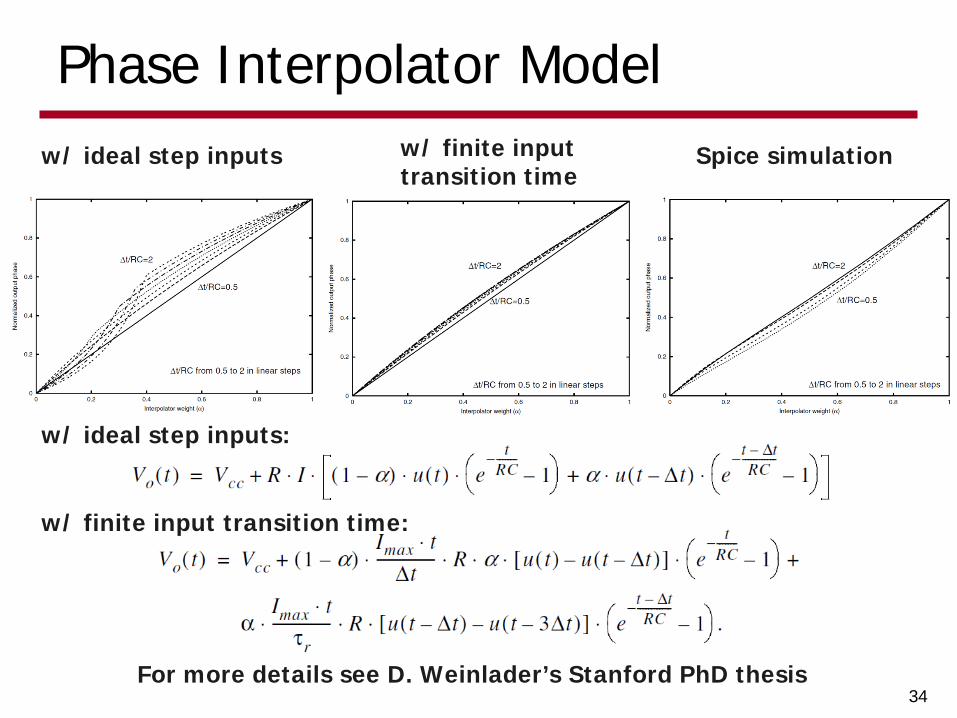
Phase Interpolator Model
34
w/ ideal step inputs w/ finite input transition time
Spice simulation
w/ ideal step inputs:
w/ finite input transition time:
For more details see D. Weinlader’s Stanford PhD thesis
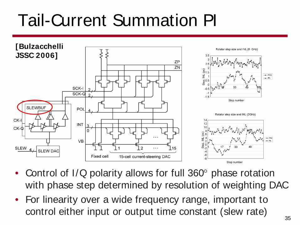
Tail-Current Summation PI
35
[Bulzacchelli JSSC 2006]
• Control of I/Q polarity allows for full 360° phase rotation with phase step determined by resolution of weighting DAC
• For linearity over a wide frequency range, important to control either input or output time constant (slew rate)

Voltage-Mode Summation PI
36
[Joshi VLSI Symp 2009]
• For linearity over a wide frequency range, important to control either input or output time constant (slew rate)
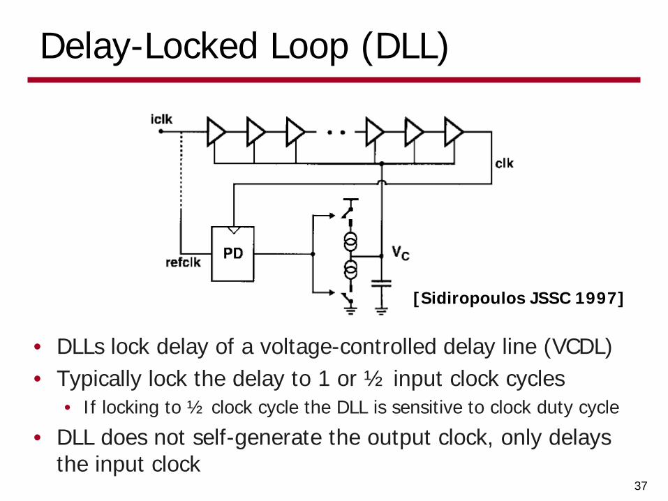
Delay-Locked Loop (DLL)
• DLLs lock delay of a voltage-controlled delay line (VCDL) • Typically lock the delay to 1 or ½ input clock cycles
• If locking to ½ clock cycle the DLL is sensitive to clock duty cycle
• DLL does not self-generate the output clock, only delays the input clock
37
[Sidiropoulos JSSC 1997]
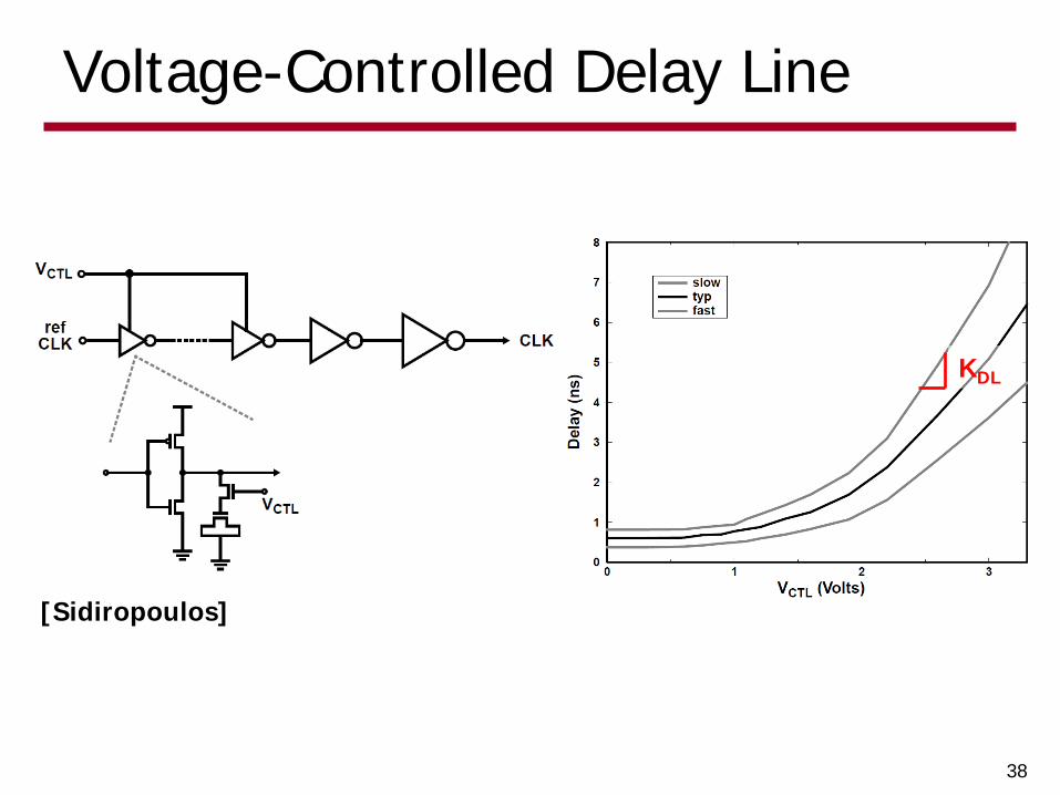
Voltage-Controlled Delay Line
38
KDL
[Sidiropoulos]
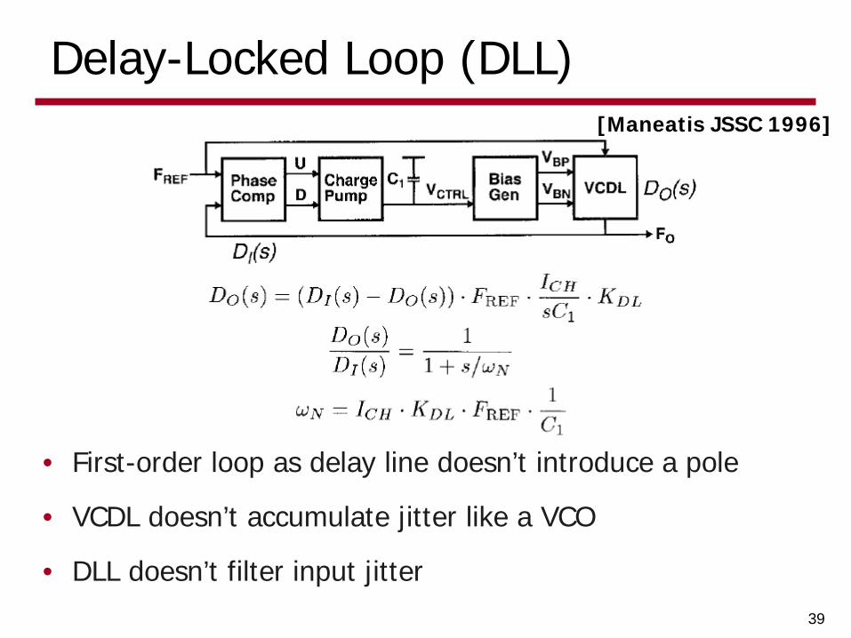
Delay-Locked Loop (DLL)
• First-order loop as delay line doesn’t introduce a pole
• VCDL doesn’t accumulate jitter like a VCO
• DLL doesn’t filter input jitter 39
[Maneatis JSSC 1996]

CDR Jitter Properties
• Jitter Transfer
• Jitter Generation
• Jitter Tolerance
40
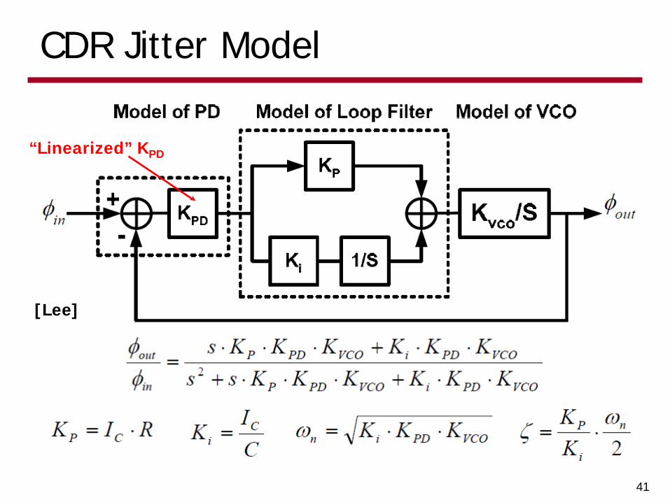
CDR Jitter Model
41
“Linearized” KPD
[Lee]
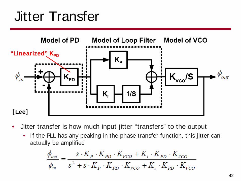
Jitter Transfer
42
“Linearized” KPD
[Lee]
• Jitter transfer is how much input jitter “transfers” to the output • If the PLL has any peaking in the phase transfer function, this jitter can
actually be amplified
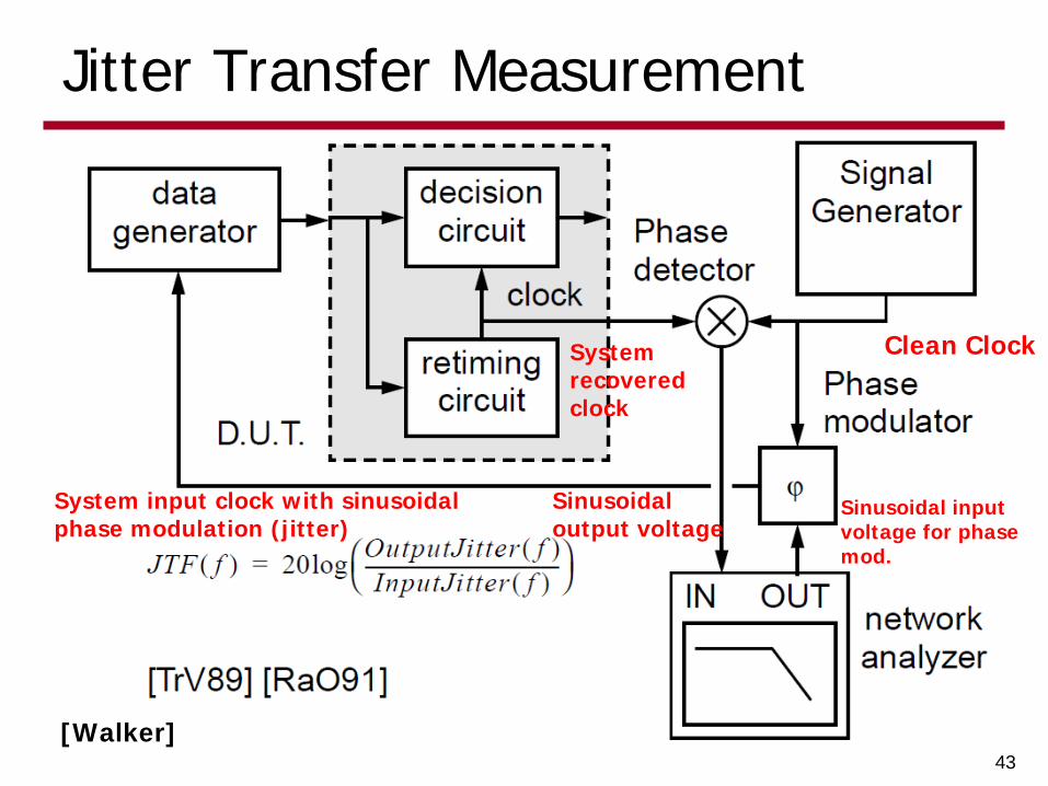
Jitter Transfer Measurement
[Walker] 43
Clean Clock
Sinusoidal input voltage for phase mod.
System input clock with sinusoidal phase modulation (jitter)
System recovered clock
Sinusoidal output voltage
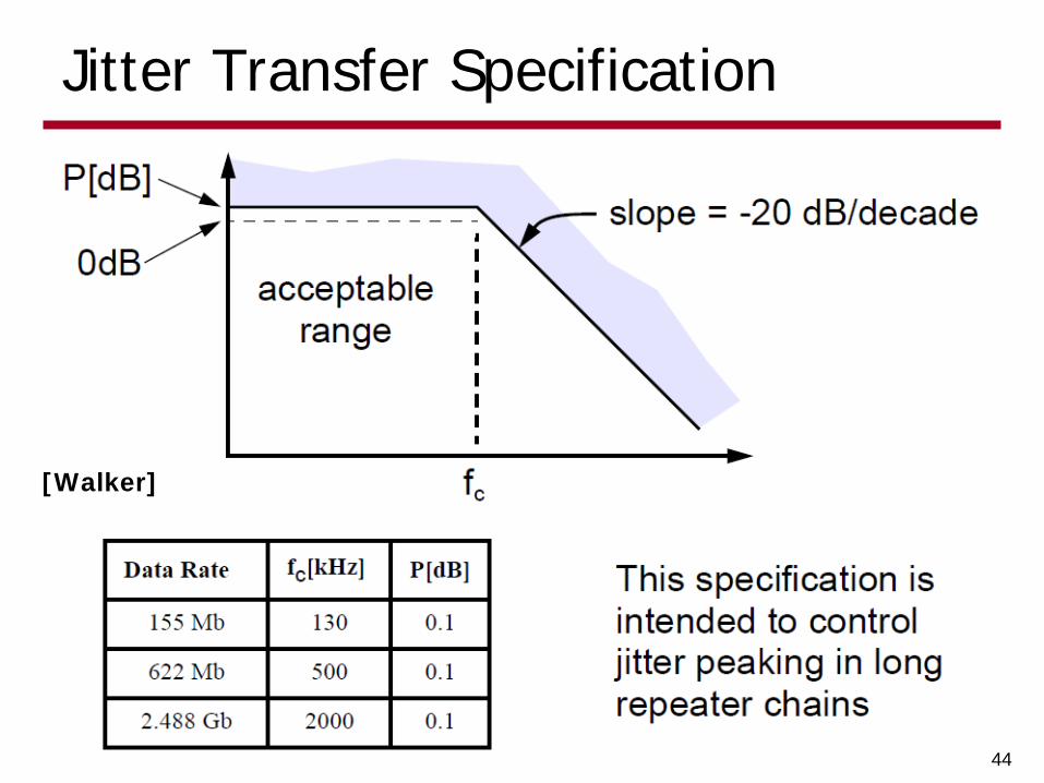
Jitter Transfer Specification
[Walker]
44

Jitter Generation
45
( ) 22
2
2
2
2 nnLoopLoopn
outn ss
s
NK
RCsN
Ks
ssHVCO
VCO ωζωφφ
++=
+
+
==VCO Phase Noise:
[Mansuri]
• Jitter generation is how much jitter the CDR “generates” • Assumed to be dominated by VCO
• Assumes jitter-free serial data input
For CDR, N should be 1

Jitter Generation
46
θout(s)θvcon(s)
20log10
High-Pass Transfer Function Jitter accumulates up to time ∝ 1/PLL bandwidth
• SONET specification: • rms output jitter ≤ 0.01 UI
[McNeill]
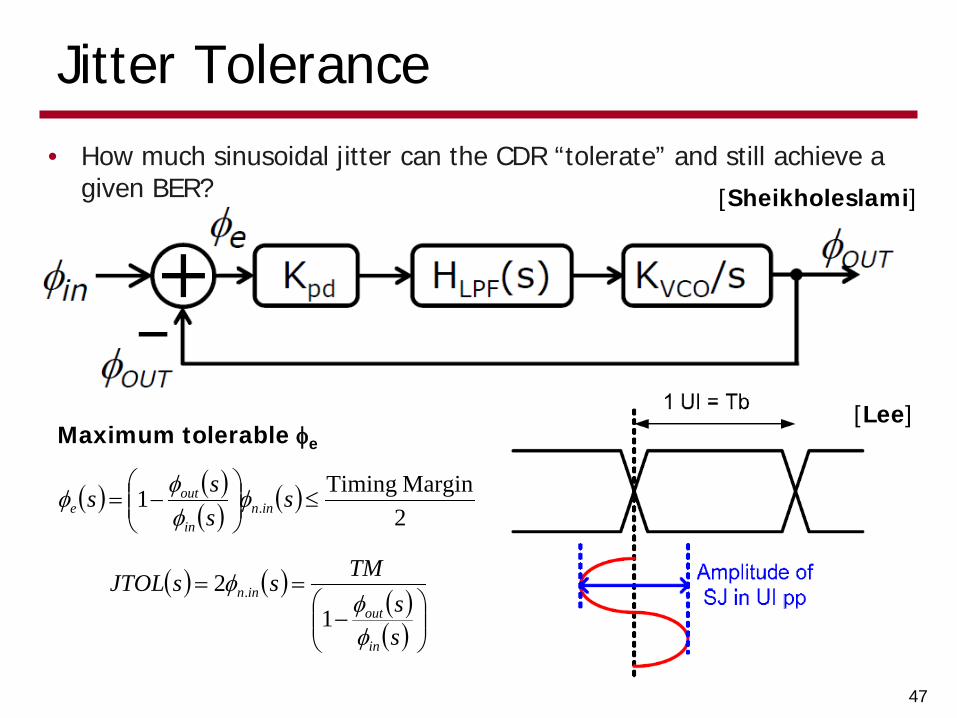
Jitter Tolerance
47
• How much sinusoidal jitter can the CDR “tolerate” and still achieve a given BER? [Sheikholeslami]
[Lee] Maximum tolerable φe
( ) ( )( ) ( )
( ) ( )( )( )
−
==
≤
−=
ss
TMssJTOL
ssss
in
outinn
innin
oute
φφ
φ
φφφφ
12
2Margin Timing1
.
.
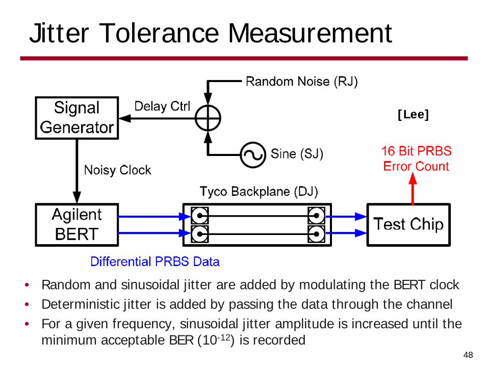
Jitter Tolerance Measurement
48
[Lee]
• Random and sinusoidal jitter are added by modulating the BERT clock • Deterministic jitter is added by passing the data through the channel • For a given frequency, sinusoidal jitter amplitude is increased until the
minimum acceptable BER (10-12) is recorded
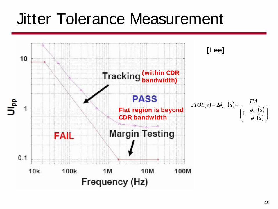
Jitter Tolerance Measurement
49
[Lee]
( ) ( )( )( )
−
==
ss
TMssJTOL
in
outinn
φφ
φ1
2 .Flat region is beyond CDR bandwidth
(within CDR bandwidth)
Next Time
• Forwarded-Clock Deskew Circuits • Clock Distribution Techniques
50