![ECEN620: Network Theory Broadband Circuit Design Fall 2014 · 2020. 10. 30. · Multiphase Clock Generation ... • Sinusoidal • Linear [Bulzacchelli] [Weinlader] 15. DLL Frequency](https://static.fdocuments.us/doc/165x107/60eb74e02337a65b583b6c1e/ecen620-network-theory-broadband-circuit-design-fall-2014-2020-10-30-multiphase.jpg)
ECEN620: Network Theory Broadband Circuit Design …spalermo/ecen620/lecture19_ee620… · ·...
51
Sam Palermo Analog & Mixed-Signal Center Texas A&M University ECEN620: Network Theory Broadband Circuit Design Fall 2014 Lecture 19: High-Speed Transmitters
Transcript of ECEN620: Network Theory Broadband Circuit Design …spalermo/ecen620/lecture19_ee620… · ·...

Sam PalermoAnalog & Mixed-Signal Center
Texas A&M University
ECEN620: Network TheoryBroadband Circuit Design
Fall 2014
Lecture 19: High-Speed Transmitters

Announcements
• Exam 3 is on Friday Dec 5• Focus on Lecture 15 (DLLs) to 19 (HS TX)• One standard size note sheet allowed• Bring your calculator
• Project Final Report Due Tuesday Dec. 9
• Project Presentations Tuesday Dec 16 at 8AM
2

Agenda
• TX Driver Circuits• Electrical Drivers• Optical Drivers
• Modulation Schemes
• Multiplexer Circuits
3

High-Speed Electrical Link System
4

Differential Signaling
• A difference between voltage or current is sent between two lines
• Requires 2x signal lines relative to single-ended signaling, but less return pins
• Advantages• Signal is self-referenced• Can achieve twice the signal swing• Rejects common-mode noise• Return current is ideally only DC
5
[Sidiropoulos]

Current vs Voltage-Mode Driver• Signal integrity considerations (min. reflections) requires
50Ω driver output impedance
• To produce an output drive voltage• Current-mode drivers use Norton-equivalent parallel termination
• Easier to control output impedance• Voltage-mode drivers use Thevenin-equivalent series
termination• Potentially ½ to ¼ the current for a given output swing
6
D+
D-
2VSWVZcont
D+
D-

Current-Mode Logic (CML) Driver
7
• Used in most high performance serial links• Low voltage operation relative to push-pull driver
• High output common-mode keeps current source saturated
• Can use DC or AC coupling• AC coupling requires data coding
• Differential pp RX swing is IR/2 with double termination

Current-Mode Current Levels
8
RV
I ppd,
IRVRIV
RIV
ppd
d
d
,
0,
1,
22
Single-Ended Termination
Differential Termination
RV
I ppd,
IRVRIV
RIV
ppd
d
d
,
0,
1,
2424

Voltage-Mode Current Levels
9
2RV
I ppd,
RVI
VVVV
VV
s
sppd
sd
sd
2
22
,
1,
1,Single-Ended Termination
Differential Termination
4RV
I ppd,
RVI
VVVV
VV
s
sppd
sd
sd
4
22
,
1,
1,

Current-Mode vs Voltage-Mode Summary
• An ideal voltage-mode driver with differential RX termination enables a potential 4x reduction in driver power
• Actual driver power levels also depend on• Output impedance control• Pre-driver power• Equalization implementation
10
Driver/Termination Current Level Normalized Current Level
Current-Mode/SE Vd,pp/Z0 1x
Current-Mode/Diff Vd,pp/Z0 1x
Voltage-Mode/SE Vd,pp/2Z0 0.5x
Voltage-Mode/Diff Vd,pp/4Z0 0.25x

• Voltage-mode driver implementation depends on output swing requirements
• For low-swing (<400-500mVpp), an all NMOS driver is suitable
Low-Swing Voltage-Mode Drivers
11
Term) (Diff. 34
11 ODts VVVDDV Term) (SE 2 11 ODts VVVDDV

• Voltage-mode driver implementation depends on output swing requirements
• For high-swing, CMOS driver is used
High-Swing Voltage-Mode Drivers
12
11 ODts VVV

Low-Swing VM Driver Impedance Control
13
• A linear regulator sets the output stage supply, Vs
• Termination is implemented by output NMOS transistors• To compensate for PVT and varying output swing levels, the pre-drive
supply is adjusted with a feedback loop• The top and bottom output stage transistors need to be sized
differently, as they see a different VOD
[Poulton JSSC 2007]

High-Swing VM Driver Impedance Control
14
• High-swing voltage-mode driver termination is implemented with a combination of output driver transistors and series resistors
• To meet termination resistance levels (50), large output transistors are required• Degrades potential power savings vs current-mode driver
[Kossel JSSC 2008] [Fukada ISSCC 2008]
(Segmented for 4-tap TX equalization)

Current-Mode Driver Example
15

Voltage-Mode Driver Example
16

Agenda
• TX Driver Circuits• Electrical Drivers• Optical Drivers
• Modulation Schemes
• Multiplexer Circuits
17

Optical Modulation Techniques
• Due to it’s narrow frequency (wavelength) spectrum, a single-longitudinal mode (SLM) laser source often generates the optical power that is modulated for data communication
• Two modulation techniques• Direct modulation of laser• External modulation of continuous-wave (CW) “DC”
laser with absorptive or refractive modulators
18

• Directly modulating laser output power• Simplest approach• Introduces laser “chirp”, which is unwanted frequency
(wavelength) modulation• This chirp causes unwanted pulse dispersion when passed
through a long fiber
Directly Modulated Laser
19
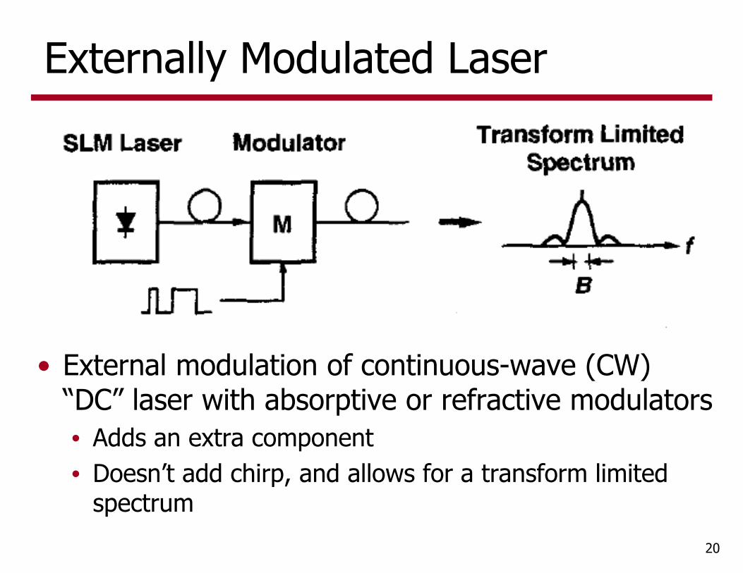
• External modulation of continuous-wave (CW) “DC” laser with absorptive or refractive modulators• Adds an extra component• Doesn’t add chirp, and allows for a transform limited
spectrum
Externally Modulated Laser
20

Extinction Ratio
• In optical communication systems, a finite optical power is generally transmitted for a “zero” symbol due to• Laser turn-on delay below threshold current• External modulator non-idealities and driver voltage swing
limitations
• The ratio between the “one”, P1, and “zero”, P0, power is the extinction ratio
21
0
1 Ratio ExtinctionPPER

Extinction Ratio Power Penalty• Optical receiver sensitivity is often specified in terms of the average
optical power necessary for the target BER
22
201 PPP • For the same average optical power, a finite extinction ratio reduces
the signal swing that the receiver sees, which is what really determines the BER
• To restore the original signal swing, more average transmitted power is necessary, quantified by an extinction ratio power penalty
11
ERERPP

Extinction Ratio Power Penalty
23
(1.76dB) 5.11-515PP
in results (6.99dB) 5An
11
ER
ERERPP

Optical Sources for Chip-to-Chip Links
• Vertical-Cavity Surface-Emitting Laser (VCSEL)
• Mach-Zehnder Modulator (MZM)
• Electro-Absorption Modulator (EAM)
• Ring-Resonator Modulator (RRM)
24

Vertical-Cavity Surface-Emitting Laser (VCSEL)
• VCSEL emits light perpendicular from top (or bottom) surface
• Important to always operate VCSEL above threshold current, ITH, to prevent “turn-on delay” which results in ISI
• Operate at finite extinction ratio (P1/P0)
25
ITH = 700A = 0.37mW/mA
AW Efficiency Slope
IP
IIP THo
VCSEL Cross-Section VCSEL L-I-V Curves

Mach-Zehnder Modulator (MZM)
26
• Refractive modulator which splits incoming light into two paths, induces a voltage-controlled phase shift in the two paths, and recombines the light in or out of phase
• While typically higher power relative to EAM or RRM, they are less sensitive to temperature variations
• For analog communication applications, modulator cosine transfer function can limit linearity
[Analui JSSC 2006]

Electro-Absorption Modulator (EAM)
• Absorption edge shifts with changing bias voltage due to the “quantum-confined Stark or Franz-Keldysh effect” & modulation occurs
• Modulators can be surface-normal devices or waveguide-based
• Maximizing voltage swing allows for good contrast ratio over a wide wavelength range
• Devices are relatively small and can be treated as lump-capacitance loads
• 10 – 500fF depending on device type27
Surface Normal EAM*
Waveguide EAM [Liu 2008]
[Helman JSTQE 2005]

Ring-Resonator Modulator (RRM)
• Refractive devices which modulate by changing the interference light coupled into the ring with the waveguide light
• Devices are relatively small (ring diameters < 20m) and can be treated as lumped capacitance loads (~10fF)
• Devices can be used in WDM systems to selectively modulate an individual wavelength or as a “drop” filter at receivers
28
[Young ISSCC 2009]

Wavelength Division Multiplexing w/ Ring Resonators
• Ring resonators can act as both modulators and add/drop filters to steer light to receivers or switch light to different waveguides
• Potential to pack >100 waveguides, each modulated at more than 10Gb/s on a single on-chip waveguide with width <1m (pitch ~4m)
29
[Rabus]

VCSEL Drivers
• Current-mode drivers often used due to linear L-I relationship
• Equalization can be added to extend VCSEL bandwidth for a given current density
30
Current-Mode VCSEL Driver VCSEL Driver w/ 4-tap FIR Equalization
[Palermo ESSCIRC 2006]

31
VCSEL TX Optical Testing
Wirebonded 10Gb/s VCSEL

32
VCSEL 16Gb/s Optical Eye Diagrams
Iavg=6.2mA, ER=3dB
w/ Equalization
IDC = 4.37mAIMOD = 3.66mA
IDC = 3.48mAI= -0.70mAI0 = 4.36mAI1 = -0.19mAI2 = 0.19mA
Equalization increases vertical eye opening
45% at 16Gb/s
No Equalization
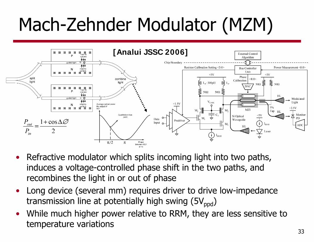
Mach-Zehnder Modulator (MZM)
• Refractive modulator which splits incoming light into two paths, induces a voltage-controlled phase shift in the two paths, and recombines the light in or out of phase
• Long device (several mm) requires driver to drive low-impedance transmission line at potentially high swing (5Vppd)
• While much higher power relative to RRM, they are less sensitive to temperature variations
33
[Analui JSSC 2006]

CMOS Modulator Driver
• Simple CMOS-style voltage-mode drivers can drive EAM and RRM due to their small size
• Device may require swing higher than nominal CMOS supply• Pulsed-Cascode driver can
reliably provide swing of 2xVdd (or 4xVdd) at up to 2FO4 data rate
34
Pulsed-Cascode Driver
[Palermo ESSCIRC 2006]

High-Voltage Output Stage Issues
35
Cascode Driver*
Vds stress on MN2 > 45% Vdd
Cascode driver has potential for 2x Vdd drive at high speed
Static-biased cascode suffers from Vds stress during transients[*Woodward PTL 1997]

Pulsed-Cascode Output Stage
36
Vds stress < 10% Vdd
• Preserves two-transistor stack configuration for maximum speed
• Cascode transistors’ gates pulsed during transitions to prevent Vds overstress
[Palermo ESSCIRC 2006]

EAM (MQWM) TX Testing
37
Electrical sampler at modulator transmitter output
16Gb/s data subsampled at modulator driver output node
[Roth JLT 2007]
Agenda
• TX Driver Circuits• Electrical Drivers• Optical Drivers
• Modulation Schemes
• Multiplexer Circuits
38

Modulation Schemes
39
• Binary, NRZ, PAM-2• Simplest, most common modulation format
• PAM-4• Transmit 2 bits/symbol• Less channel equalization and circuits run ½ speed
• Duobinary• Allows for controlled ISI, symbol at RX is current bit plus preceding bit• Results in less channel equalization
1 nxnxnw
0
1
00
01
11
10
0, if x[n-1]=0
1, if x[n-1]=0 OR
0, if x[n-1]=1
1, if x[n-1]=1
No Pre-Coding Case

Modulation Frequency Spectrum
40
Majority of signal power in 1GHz bandwidth
Majority of signal power in 0.5GHz bandwidth
Majority of signal power in 0.5GHz bandwidth

Agenda
• TX Driver Circuits• Electrical Drivers• Optical Drivers
• Modulation Schemes
• Multiplexer Circuits
41
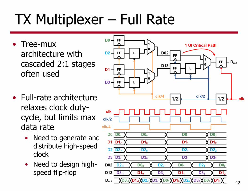
TX Multiplexer – Full Rate
42
• Tree-muxarchitecture with cascaded 2:1 stages often used
• Full-rate architecture relaxes clock duty-cycle, but limits max data rate• Need to generate and
distribute high-speed clock
• Need to design high-speed flip-flop

TX Multiplexer – Full Rate Example
43
[Cao JSSC 2002]
• CML logic sometimes used in last stages• Minimize CML to save
power
• 10Gb/s in 0.18m CMOS
• 130mW!!
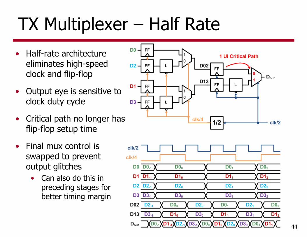
TX Multiplexer – Half Rate
44
• Half-rate architecture eliminates high-speed clock and flip-flop
• Output eye is sensitive to clock duty cycle
• Critical path no longer has flip-flop setup time
• Final mux control is swapped to prevent output glitches• Can also do this in
preceding stages for better timing margin

Clock Distribution Speed Limitations
• Max clock frequency that can be efficiently distributed is limited by clock buffers ability to propagate narrow pulses
• CMOS buffers are limited to a min clock period near 8FO4 inverter delays• About 4GHz in typical 90nm
CMOS• Full-rate architecture limited
to this data rate in Gb/s
• Need a faster clock use faster clock buffers• CML• CML w/ inductive peaking
45
Clock Amplitude Reduction*
*C.-K. Yang, “Design of High-Speed Serial Links in CMOS," 1998.
tFO4 in 90nm ~ 30ps
faster slower

Multiplexing Techniques – ½ Rate
• Full-rate architecture is limited by maximum clock frequency to 8FO4 Tb
• To increase data rates eliminate final retiming and use multiple phases of a slower clock to mux data
• Half-rate architecture uses 2 clock phases separated by 180 to mux data• Allows for 4FO4Tb
• 180 phase spacing (duty cycle) critical for uniform output eye
46

2:1 CMOS Mux
• 2:1 CMOS mux able to propagate a minimum pulse near 2FO4 Tb
• However, with a ½-rate architecture still limited by clock distribution to 4FO4 Tb• 8Gb/s in typical 90nm
47
*C.-K. Yang, “Design of High-Speed Serial Links in CMOS," 1998.
faster slower

2:1 CML Mux
• CML mux can achieve higher speeds due to reduced self-loading factor• Cost is higher power consumption that is independent of data
rate (static current)48
[Razavi]

Increasing Multiplexing Factor – ¼ Rate
• Increase multiplexing factor to allow for lower frequency clock distribution
• ¼-rate architecture• 4-phase clock distribution
spaced at 90 allows for 2FO4 Tb
• 90 phase spacing and duty cycle critical for uniform output eye
49

Increasing Multiplexing Factor – Mux Speed
• Higher fan-in muxes run slower due to increased cap at mux node
• ¼-rate architecture• 4:1 CMOS mux can potentially
achieve 2FO4 Tb with low fanout• An aggressive CMOS-style design has
potential for 16Gb/s in typical 90nm CMOS
• 1/8-rate architecture• 8-phase clock distribution spaced at
45 allows for 1FO4 Tb• No way a CMOS mux can achieve
this!!
50*C.-K. Yang, “Design of High-Speed Serial Links in CMOS," 1998.
<10% pulse width closure
select signal
2:1 8:1

Next Time
• High-Speed I/O Overview
51
![ECEN620: Network Theory Broadband Circuit Design Fall 2019ece.tamu.edu/~spalermo/ecen620/lecture07_ee620_vcos.pdf• VCO Jitter 23. Oscillator Noise 24 Jitter [McNeill] Phase Noise](https://static.fdocuments.us/doc/165x107/5eb0f0afdb23476d411ded00/ecen620-network-theory-broadband-circuit-design-fall-spalermoecen620lecture07ee620vcospdf.jpg)