ECEN 720 High-Speed Links Circuits and Systems Lab4 ...spalermo/ecen689/ECEN720_lab4_2013.pdf3....
13
1 ECEN 720 High-Speed Links Circuits and Systems Lab4 –Receiver Circuits Objective To learn fundamentals of receiver circuits. Introduction Receivers are used to recover the data stream transmitted by transmitters. The voltage and time domain resolution and offset are the key performance specs for receiver circuits. In this lab, the receiver building blocks will be studied and practiced. Their performance metrics are going to be characterized. Receiver Parameters A receiver’s performance is measured in both time and voltage domain. How small voltage a receiver can measure is the sensitivity. The receiver’s voltage offset is the similar concept as a comparator’s input offset voltage, which is caused by the device mismatch and circuit structure. In time domain, the shortest pulse width the receiver can detect is called the aperture time. It limits the maximum data rate of the link system. The time offset becomes the timing skew and jitter between the receiver and some reference timing marker (CDR). These four parameters are illustrated in Figure 1. Figure 1 Eye Diagram Showing Time and Voltage Offset and Resolution [Dally] Basic Receiver Block Diagram Pre-amplifier is often used in the receiver side to improve signal gain and reduce input referred noise. It must provide gain at high frequency bandwidth so that it does not attenuate high frequency data. It can also operate as a common mode shifter to correct the common mode
Transcript of ECEN 720 High-Speed Links Circuits and Systems Lab4 ...spalermo/ecen689/ECEN720_lab4_2013.pdf3....
1
ECEN 720 High-Speed Links Circuits and Systems
Lab4 –Receiver Circuits
Objective To learn fundamentals of receiver circuits.
Introduction Receivers are used to recover the data stream transmitted by transmitters. The voltage and time domain resolution and offset are the key performance specs for receiver circuits. In this lab, the receiver building blocks will be studied and practiced. Their performance metrics are going to be characterized.
Receiver Parameters A receiver’s performance is measured in both time and voltage domain. How small voltage a receiver can measure is the sensitivity. The receiver’s voltage offset is the similar concept as a comparator’s input offset voltage, which is caused by the device mismatch and circuit structure. In time domain, the shortest pulse width the receiver can detect is called the aperture time. It limits the maximum data rate of the link system. The time offset becomes the timing skew and jitter between the receiver and some reference timing marker (CDR). These four parameters are illustrated in Figure 1.
Figure 1 Eye Diagram Showing Time and Voltage Offset and Resolution [Dally]
Basic Receiver Block Diagram Pre-amplifier is often used in the receiver side to improve signal gain and reduce input referred noise. It must provide gain at high frequency bandwidth so that it does not attenuate high frequency data. It can also operate as a common mode shifter to correct the common mode

2
mismatch between TX and RX. Offset correction can also implemented in the pre-amplifier. The comparator/sampler can be implemented with static amplifiers or clocked regenerative amplifiers. If the power consumption is a concern, clocked regenerative amplifier is preferred.
Figure 2 Basic Receiver Block Diagram
Clocked Comparators Clocked comparators can sample the input signals at clock edges and resolves the differential. They are also called regenerative amplifier, sense-amplifier, or latch. Two clocked comparators are shown in Figure 3. A flip-flop can be made of cascading an R-S latch after strong-arm as shown in Figure 4. It also can be formed by cascading two CML latches.
Figure 3 Clocked Comparators (a) Strong-Arm Latch (b) CML Latch
Figure 4 Flip-Flop made of a Strong-Arm Comparator and an RS Latch

3
Clocked Comparator LTV Model and ISF A comparator can be viewed as a noisy nonlinear filter followed by an ideal sampler and slicer (comparator) as shown in Figure 5 [2]. The small-signal comparator response can be modeled with an ISF of
Γ(𝜏) = ℎ(𝑡, 𝜏) (1)
The comparator ISF is a subset of a time-varying impulse response h(t,τ) for LTV system, which can be expressed as
𝑦(𝑡) = ℎ(𝑡, 𝜏)𝑥(𝜏)𝑑𝜏∞
−∞ (2)
where h(t,τ) is the system response at t to a unit impulse arriving at τ and for LTI system h(t,τ)= h(t-τ) using convolution. Output voltage of comparator can be expressed as
𝑉𝑜(𝑡𝑜𝑏𝑠) = 𝑉𝑖(𝜏)Γ(𝜏)𝑑𝜏∞
−∞ (3)
and the comparator decision can be calculated as
𝐷𝐾 = 𝑠𝑔𝑛(𝑉𝐾) = 𝑠𝑔𝑛𝑉𝑜(𝑡𝑜𝑏𝑠 + 𝐾𝑇) = 𝑠𝑔𝑛 𝑉𝑖(𝜏)Γ(𝜏)𝑑𝜏∞
−∞ (4)
Please refer to [2] for details.
Figure 5 Clocked Comparator LTV Model
Characterizing Comparator ISF using Cadence The characterization of a comparator’s ISF can be found in [2]. The simulation block diagram is shown in Figure 6. A small step signal is applied to the comparator at time τ with a small offset voltage. The offset voltage is generated through a simple servo loop, which makes the comparator metastable. The Vmetastable is measured for various time τ to obtain the step sensitivity

4
function SSF (τ). Cadence simulation setup is shown in Figure 7. Both input step and clock signals are set to be the same frequency and with time τ delay. At the metastable condition, the flip-flop generates equal number of 1s and 0s. The percentage of 1s and 0s controls the average current flow direction of the voltage control current source (VCCS) which generates an offset voltage on the shunt capacitor. The simulation can be done by sweeping the time τ and measure the offset voltage. ISF can be eventually generated from those simulation results [2]. Please also refer to the appendix in this lab.
Figure 6 Characterization of Comparator ISF [Jeeradit VLSI 2008]
Figure 7 Cadence Comparator ISF Setup

5
Pre-Lab
1. Generally circuits are designed to handle a minimum variation range of ±3α. What is the yield rate for ±α, ±2α, ±3α, and ±4α?
Figure 8 Gaussian distribution
2. A receiver is characterized by its input sensitivity which represents the voltage resolution, and by the set-up and hold times (tS and tH) which represent the timing resolution as illustrated as light rectangle in Fig. 1. The center of the dark rectangle is shifted by the offset time and offset voltage from the center of the light rectangle. Input sensitivity consists of input voltage offset, input referred noise, and min latch resolution voltage. A Strong-Arm latch’s Input static voltage offset is 8mV, minimum latch resolution from hysteresis is bounded to 2mV, and 14mV input referred noise at the target BER of 10-12. The aperture time and the combined set-up and hold time (tS+tH) of the latch is 10ps and 20ps, respectively. Assume also that the receiver sampling clock has a 10ps timing offset and 14ps jitter at the target BER of 10-12. On the B12 Backplane 6.4Gb/s NRZ eye diagram obtained in the Lab 2 (either from MATLAB or CADENCE), draw the window that the incoming signal needs to avoid such that the receiver will reliably translate the voltage waveform received from the channel into logic 1s or 0s under worst-case combinations of offsets and resolution.
3. Demultiplexer is often used to deserialize a stream of high speed data. It can be
implemented after the receiver circuit to generate lower speed data. Please design a 1:4 Binary-tree DeMUX that de serializes 8Gb/s data into 2Gb/s data. Figure 9 is an example of 1:2 De-MUX, please refer to [3] as a reference. You may use behavioral models to implement the De-Mux and show your simulation results.
Q
QSET
CLR
D
Q
QSET
CLR
Dt
t
t
t
Q
QSET
CLR
D t
t
Data
CLKin
CLKin
A
B
DFF
DFF Latch

6
Figure 9 1:2 Data De-MUX [3]
Questions
1. High-Speed Comparator Design. This problem involves the design of 4 different high-speed comparators to meet the following specifications: a. clk → Dout delay ≤ 200ps with a 10mV static differential input voltage (Din+-Din-) at
a common mode voltage of 80%*VDD. Measure delay from when the clock is at 50% VDD to Dout+ is at 50% VDD for an output rising transition. Please refer to Figure 18.
b. Clock frequency = 2.5GHz. Use at least one inverter-based buffer to clock your circuit for realistic clock waveforms.
c. Load cap on Dout+ and Dout- is 10fF. d. Input referred offset σ ≤ 10mV. Here you can optimistically assume that the input
referred offset is just due to the input differential pair Vt mismatch and use the mismatch equation given in the notes, i.e. no need to run Monte Carlo simulations.
e. Optimize the design for power consumption, i.e. don’t overdesign for a supper small delay. Try to minimize total capacitance while still meeting the 200ps delay and offset specifications.
a. Conventional Strong-Arm Latch. For an example schematic, refer to Figure 4 in Design the comparators based on the following 4 architectures:
[4]. Feel free to change the pre-charge transistors configuration if you desire.
b. CML Latch. For an example schematic, refer to Figure 11a in [5].
c. Schinkel Low-Voltage Latch. For an example schematic, refer to Figure 2 in [6].
d. Goll Low-Voltage Latch. For an example schematic, refer to Figure 2 in [7].
a. As shown in The comparators should realize a flip-flop function.
Figure 10, for the Strong-Arm type latches (1, 3, and 4) follow with the optimized SR-latch shown in Figure 11. For more details on the optimized SR-latch, refer to [8] Note: for architecture (3) you will need to modify this optimized SR-latch – as the sense-amp pre-charges to GND (vs VDD in 1 & 4).
b. To realize a CML flip-flop with architecture (2), simply cascade 2 CML latches to realize a master-slave flip-flop.

7
Figure 10 High-Speed Comparator
Figure 11 Optimized SR Latch

8
2. High-Speed Comparator Characterization. Please read [2] and [9]. Please simulate all FOUR comparators and produce the following using 500MHz Clock signal:
a. Plot comparator delay vs. VDD for VDD varying from 50% of nominal VDD to 100% VDD. For this keep the input common mode equal to 80% of the supply, i.e. sweep the input common-mode along with the supply. Also scale the clock input signal level with VDD.
b. Plot comparator power vs. VDD in a similar manner. c. Generate the comparator Impulse Sensitivity Function (ISF) at the nominal VDD,
80%VDD and 60%VDD (3 curves). Again, track the input common-mode with VDD. To do this use the equivalent test circuit in Slide 9 of Lecture 14, for more details refer to [2] For the characterization try an input differential step input of 50mV, i.e. VCM±25mV for the differential input signals. Report the comparator aperture time, by measuring the 10%-90% “rise-time” from simulation. Please refer to [9] for the aperture time measurement.
d. Please compare the design of these FOUR latches. You can refer to [2]
3. Link Verification. The comparator designed can be considered as a basic receiver. Please build a 5Gb/s link system by using the transmitter designed either in voltage mode or current mode and the comparator which you chosen for the best performance. Please refer to Figure 12. Use 50Ω transmission line with 1ns delay. Add 200fF parasitic caps at the output of your transmitter. Feel free to choose the best termination and coupling schemes.
a. Please show the circuit schematic including coupling and termination. b. Explain why you choose your coupling and termination scheme. c. Please show simulation results and eye diagram and verify the link performance.
Figure 12 Basic Link System using DC Coupling
Zo1=50Ω
Zo2=50Ω RXTXPRBS 100Ω C1=10fF
C1=10fF
C1=200f
C1=200fF
Pre-Driver
Td=1ns
C1=200f
C1=200fF

9
Reference [1] Digital Systems Engineering, W. Dally and J. Poulton, Cambridge University Press, 1998.
[2] M. Jeeradit , J. Kim , B. S. Leibowitz , P. Nikaeen , V. Wang , B. Garlepp and C.
Werner "Characterizing sampling aperture of clocked comparators", Dig. Tech. Papers,
2008 Symp. VLSI Circuits, pp. 68 2008.
[3] J. Cao, M. Green, A. Momtaz, K. Vakilian, D. Chung, K.-C. Jen, M. Caresosa, X. Wang,
W.-G. Tan, Y. Cai, I. Fujimori, and A. Hairapetian, “OC-192 transmitter and receiver in
standard 0.18-_m CMOS,” IEEE J. Solid-State Circuits, vol. 37, pp. 1768–1780, Dec.
2002.
[4] J. Kim et al., “Simulation and Analysis of Random Decision Errors in Clocked
Comparators,” IEEE Transactions on Circuits and Systems - I, vol. 56, no. 8, Aug. 2009,
pp. 1844-1857.
[5] T. Toifl et al., “A 22-Gb/s PAM-4 Receiver in 90-nm CMOS SOI Technology,” IEEE
Journal of Solid-State Circuits, vol. 41, no. 4, Apr. 2006, pp. 954-965.
[6] D. Schinkel et al., “A Double-Tail Latch-Type Voltage Sense Amplifier with 18ps
Setup+Hold Time,” IEEE International Solid-State Circuits Conference, Feb. 2007.
[7] B. Goll and H. Zimmermann, “A Comparator with Reduced Delay Time in 65-nm CMOS
for Supply Voltages Down to 0.65V,” IEEE Transactions on Circuits and Systems - II,
vol. 56, no. 11, Nov. 2009, pp. 810-814.
[8] B. Nikolic et al., “Improved Sense-Amplifier-Based Flip-Flop: Design and
Measurements,” IEEE Journal of Solid-State Circuits, vol. 35, no. 6, June 2000, pp. 876-
884.
[9] H. O. Johansson and C. Svensson, "Time resolution of NMOS sampling switches used
on low-swing signals", IEEE J. Solid-State Circuits, vol. 33, pp. 237 - 245, 1998.

10
Appendix ISF simulation steps:
Figure 13 Transient Simulation of ISF Test Circuit at time τ
Figure 14 Direct Plot of Vms at each time τ after parametric sweep
11
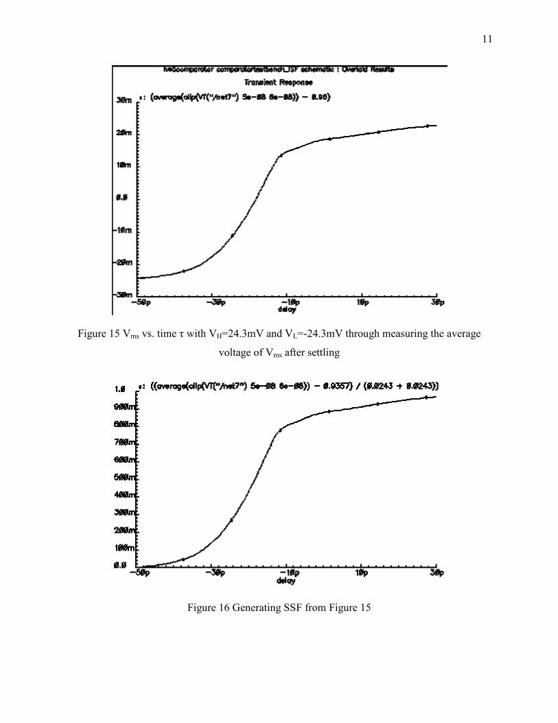
Figure 15 Vms vs. time τ with VH=24.3mV and VL=-24.3mV through measuring the average
voltage of Vms after settling
Figure 16 Generating SSF from Figure 15
12
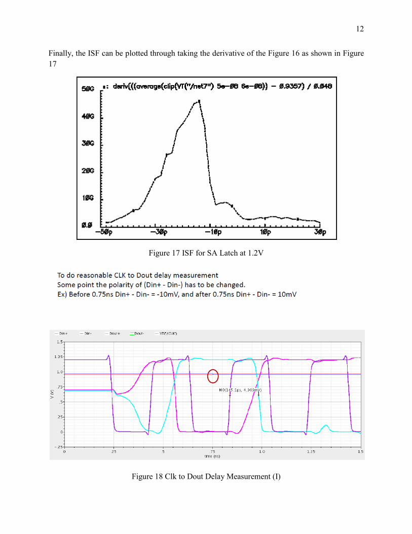
Finally, the ISF can be plotted through taking the derivative of the Figure 16 as shown in Figure 17
Figure 17 ISF for SA Latch at 1.2V
Figure 18 Clk to Dout Delay Measurement (I)

13
Figure 19 Clk to Dout Delay Measurement (II)