Development Status of Canon’s EUVL Exposure...
17
Slide 1 Slide 1 1 1 February 26, 2009 7271-68 Slide 1 International EUVL Symposium, October 19-21, Prague Slide 1 Development Status of Development Status of Canon Canon ’ ’ s EUVL Exposure Tool s EUVL Exposure Tool Akira Miyake, Takayuki Hasegawa, Hiroyuki Kubo, Shigeyuki Uzawa Canon Inc.
Transcript of Development Status of Canon’s EUVL Exposure...

Slide 1Slide 11 1February 26, 2009 7271-68 Slide 1International EUVL Symposium, October 19-21, Prague Slide 1
Development Status of Development Status of CanonCanon’’s EUVL Exposure Tools EUVL Exposure Tool
Akira Miyake, Takayuki Hasegawa,Hiroyuki Kubo, Shigeyuki Uzawa
Canon Inc.

Slide 2Slide 22 2February 26, 2009 7271-68 Slide 2International EUVL Symposium, October 19-21, Prague Slide 2
Outline Outline
Development schedule- EUVL exposure tool roadmap
Mirror fabrication and evaluation- Surface figuring
- Multilayer evaluation
Optics lifetime- Atomic hydrogen cleaning
Optical design- 6-mirror high-NA PO
Summary

Slide 3Slide 33 3February 26, 2009 7271-68 Slide 3International EUVL Symposium, October 19-21, Prague Slide 3
EUVL Tool RoadmapEUVL Tool RoadmapITRS2008 2008 2009 2010 2011 2012 2013 2014 2015 2016 2017 2018 2019
2 year cycle (nm) 45 32 22 16 11 8DRAM (hp)
Flash (hp)57 50 45 40 36 32 28 25 23 20 18 16
45 40 36 32 28 25 23 20 18 16 14 13
HVMPlatform
HVM tool (VS3)TP Enhancement
HVM tool (VS2)NA > 0.32
SFETInstalled at SELETE
Prototype
6-mirror (PO1) NA0.3In-house test
Specifications of VS2NA > 0.32
Aberration < 0.35 nm RMS
Flare 5 %
Dense Lines < 25nm
Isolated lines 17nm
Dense Contacts < 28nm
Overlay (SMO) < 3 nm
Throughput 100wph@200w IF10mJ/cm2

Slide 4Slide 44 4February 26, 2009 7271-68 Slide 4International EUVL Symposium, October 19-21, Prague Slide 4
PO1 SystemPO1 System
PO1 is being fabricated to evaluate and improve our fabrication technology.
FeaturesLow-thermal expansion ceramic structure.Position of 5 mirrors are controlled in real time.
High stability of mirror position against vibration.Aberration can be compensated.
Mirrors
NA 0.3
Slit size 26 x 2 mm2
Aberration 0.55 nm RMS
Flare 7 %

Slide 5Slide 55 5February 26, 2009 7271-68 Slide 5International EUVL Symposium, October 19-21, Prague Slide 5
0
0.5
1
1.5
2
2.5
0 0.25 0.5 0.75 1 1.25 1.5 1.75 2
IBF process capabilityIBF process capability
Effective spatial resolution range ; small beam IBF
Before IBF
After IBF
Figure correctionFigure correction
Effective range
F=0.88mm-1 (λ=1.2mm)
Spatial frequency(mm-1)
Pow
er
◆Small beam operation has 1.2mm wavelength resolution.
IBF tool
EUVA

Slide 6Slide 66 6February 26, 2009 7271-68 Slide 6International EUVL Symposium, October 19-21, Prague Slide 6
1.0E-09
1.0E-08
1.0E-07
1.0E-06
1.0E-05
1.0E-04
1.0E-03
1.0E-02
1.0E-01
1.0E+00
0.01 0.1 1 10 100 1000 10000 100000 1000000
Spatial Frequency [1/mm]
Pow
er [
nm
2*
mm
]
MSFR: 53pmRMS
Figure: 38pmRMS
HSFR: 65pmRMS
Mirror Surface AccuracyMirror Surface Accuracy
Flare calculated from PSD curve is less than 5 %.(Range of spatial frequency that causes the flare is 4.5 decades.)
Figure accuracy also satisfies requirements for HVM tools.
2006
2008
2009

Slide 7Slide 77 7February 26, 2009 7271-68 Slide 7International EUVL Symposium, October 19-21, Prague Slide 7
Wavefront Error of a Multilayer MirrorWavefront Error of a Multilayer Mirror
Wavefront of reflected light is determined by-shape of the mirror surface -phase shift on multilayer reflection.
Therefore, we have to measure and control them with high accuracy.
multilayer
wavefrontwavefront
Incident beam reflected beam

Slide 8Slide 88 8February 26, 2009 7271-68 Slide 8International EUVL Symposium, October 19-21, Prague Slide 8
Reflection Phase MeasurementReflection Phase Measurement
Mo Si Mo SiSi Mo Si MoVacuum
Multilayer SurfaceIncident BeamReflected Beam
Standing wave is a superposition of the incident light and the reflected light.Electric field of the standing wave depends on phase shift and reflectivity.
Photoelectron intensity is proportional to electric field intensity on the multilayer surface approximately, because escape depth of low energy (<100eV) electron is small compared to thickness of each layer.
Photoelectrons

Slide 9Slide 99 9February 26, 2009 7271-68 Slide 9International EUVL Symposium, October 19-21, Prague Slide 9
AtAt--wavelength Multilayer Evaluation Systemwavelength Multilayer Evaluation System
P-pol
S-pol
Sample
Rotation
M1 M3
M2
0th order
1st orderMonochromatic EUV light
Beam splitter (plane grating)
CCD 2Multilayer Sample
Electron Multiplier
CCD 1
Electron
beam intensity monitor
extinction factor : <1E-3Reflectivity Repeatability : 0.2%
Features- High accuracy of wavelength (Kr gas absorption spectrum, source emission spectrum) - Reflectivity and phase measurement at same time- Polarization control
Polarizer
EUV sourceLarge sample chamber MonochromatorSample chamber
Beam intensity monitor, electron detector

Slide 10Slide 101010February 26, 2009 7271-68 Slide 10International EUVL Symposium, October 19-21, Prague Slide 10
Measured phase shift distributionMeasured phase shift distribution
Phase shift by multilayer reflection can be measured using standing wave method.Wavefront error caused by phase shift deviation was estimated to about 2mλ(σ).
Measured reflectivity and photoelectron intensity
-10
-5
0
5
10
0 50 100 150
-10
-5
0
5
10
30 60 90 120 150
radius (mm)
angle(deg)
wav
efro
nt e
rror
(m
λ)w
avef
ront
err
or
(mλ)
0
0.00000002
0.00000004
0.00000006
0.00000008
0.0000001
0.00000012
0.00000014
0.00000016
0.00000018
0
0
0
0
0
0
0
0
0
1
1
1
1
12.8 13.0 13.2 13.4 13.6 13.8
Reflectivity, photoelectron intensity
wavelength (nm)
1
radius
angle
Radial distribution
Directioanl distribution

Slide 11Slide 111111February 26, 2009 7271-68 Slide 11International EUVL Symposium, October 19-21, Prague Slide 11
Optics lifetime/Carbon depositionOptics lifetime/Carbon deposition
Carbon deposition rate was measured using SR beamlines.Repeated cleaning of deposited carbon on optical surface is needed.
Carbon deposition rate was estimatedusing experimental results under accelerated condition.-Decane gas introduced -SR beamline of Super-ALIS (NTT)
Assumption : - Decane pressure of 1E-7Pa- Linear extrapolation
Estimated carbon deposition rate of HVM exposure tool: 0.03 nm/hr (max)
Considering other factors:- EUV intensity distribution in PO- Source frequency- Residual gas species- Mitigation technologies
carbon deposition rate can be mitigated. EUVA
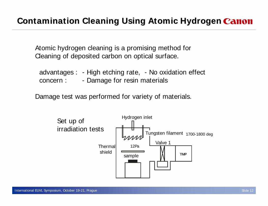
Slide 12Slide 121212February 26, 2009 7271-68 Slide 12International EUVL Symposium, October 19-21, Prague Slide 12
TMP
Valve 1
TMP
Contamination Cleaning Using Atomic HydrogenContamination Cleaning Using Atomic Hydrogen
Atomic hydrogen cleaning is a promising method forCleaning of deposited carbon on optical surface.
advantages : - High etching rate, - No oxidation effect concern : - Damage for resin materials
Damage test was performed for variety of materials.
Set up of irradiation tests
sample
Thermalshield
Tungsten filament
Hydrogen inlet
12Pa
1700-1800 deg

Slide 13Slide 131313February 26, 2009 7271-68 Slide 13International EUVL Symposium, October 19-21, Prague Slide 13
AFM (30µm range) SEM (10,000X)
Before After Before After
PTFE
THV
Epoxy
Surface Damage caused by Atomic Hydrogen IrradiationSurface Damage caused by Atomic Hydrogen Irradiation
EUVA Report2008
5 μm
2µm
Irradiation time : 180min (corresponds to the etching depth of 50nm)
Atomic hydrogen cleaning causes no significant damage to several kinds of resin material.

Slide 14Slide 141414February 26, 2009 7271-68 Slide 14International EUVL Symposium, October 19-21, Prague Slide 14
66--mirror highmirror high--NA Projection OpticsNA Projection Optics-- Target of Wavefront aberrationsTarget of Wavefront aberrations
Cross-pole illumination is chosen for HP16nm LSdue to large DOF with NILS >1.2 Target value of aberrations is <0.35nm RMSfor delta CD <1.12nm (7% of CD)
delta CD vs Aberrat ion Value
00.20.40.60.8
11.21.4
0.010 .040.070.090.120 .150.180.200.230 .260.280.310.340 .360.39
nm RMS
ΔC
D[n
m]
delta CD=1.12nm0.35nmRMS
- 1 - 0.5 0 0.5 1- 1
- 0.5
0
0.5
1
0
0.2
0.4
0.6
0.8
1
- 1 - 0.5 0 0.5 1- 1
- 0.5
0
0.5
1
0
0.2
0.4
0.6
0.8
1
SPIE2009

Slide 15Slide 151515February 26, 2009 7271-68 Slide 15International EUVL Symposium, October 19-21, Prague Slide 15
difficult to place
Large aberration
PerformanceNA : > 0.32Flare : ≦ 5%final aberration : ≦ 0.35 nmRMS
66--mirror highmirror high--NA Projection OpticsNA Projection Optics-- Optical designOptical design
difficult to place
difficult to place
All combination of 6Mirror(M5=convex, M6=concave. so, there are16 combination by M1,M2,M3 and M4 )
Best typeBest type
Negative power
Negative power
Negative power
Negative power
Difficult to image
Difficult to image
Difficult to image
Difficult to image
Difficult to place
■■Optical Design Result of Projection OpticsOptical Design Result of Projection Optics

Slide 16Slide 161616February 26, 2009 7271-68 Slide 16International EUVL Symposium, October 19-21, Prague Slide 16
SummarySummary
Fabrication technologies for projection opticsSurface figuring technologies satisfy requirements for HVM tool.At-wavelength multilayer evaluation system for thickness and phase measurements has been developed.
Optics lifetimeAtomic hydrogen cleaning method has advantage of low damage and reasonable etching rate.
Optics DesignOptical design of 6-mirror High-NA projection optics has been completed.

Slide 17Slide 171717February 26, 2009 7271-68 Slide 17International EUVL Symposium, October 19-21, Prague Slide 17
AcknowledgmentAcknowledgment
Part of this work was performed
under the management of Extreme Ultraviolet Lithography
System Development Association (EUVA)
in the Ministry of Economy Trade and Industry program
supported by
New Energy and Industrial Technology Development
Organization.