Development of the technological process for the ...elib.suub.uni-bremen.de/edocs/00102724-1.pdf ·...
143
Development of the technological process for the production of the electrostatic curved beam actuator for pneumatic microvalves Vom Fachbereich für Physik und Elektrotechnik der Universität Bremen zur Erlangung des akademischen Grades Doktor-Ingenieur (Dr.-Ing.) Genehmigte Dissertation Von M.Sc. Denis Petrov Wohnhaft in Pinneberg Referent: Prof. Dr.-Ing. W. Benecke Korreferent: Prof. Dr.-Ing. W. Lang Eingerichtet am: 21.05.2012 Tag des Promotionskolloquiums: 16.07.2012 Bremen 2012
Transcript of Development of the technological process for the ...elib.suub.uni-bremen.de/edocs/00102724-1.pdf ·...

Development of the technological process for the production
of the electrostatic curved beam actuator for pneumatic
microvalves
Vom Fachbereich für Physik und Elektrotechnik
der Universität Bremen
zur Erlangung des akademischen Grades
Doktor-Ingenieur (Dr.-Ing.)
Genehmigte Dissertation
Von
M.Sc. Denis Petrov
Wohnhaft in Pinneberg
Referent: Prof. Dr.-Ing. W. Benecke
Korreferent: Prof. Dr.-Ing. W. Lang
Eingerichtet am: 21.05.2012
Tag des Promotionskolloquiums: 16.07.2012
Bremen
2012

To my wife

Table of contents
i
Table of contents
Abstract ................................................................................................................................................................... 1
1 Chapter I: Introduction ................................................................................................................................... 2
1.1 MEMS: definition, applications, trends ....................................................................................................... 2
1.2 Overview of the basic microfabrication techniques ..................................................................................... 4
1.3 Overview of Microactuators ........................................................................................................................ 6
1.3.1 Definition and classification .................................................................................................................... 6
1.3.2 Electromagnetic actuators ........................................................................................................................ 7
1.3.3 Electrostatic actuators .............................................................................................................................. 8
1.3.4 Piezoelectric actuators ............................................................................................................................. 9
1.3.5 Thermal actuators .................................................................................................................................. 11
1.3.6 Optical actuators .................................................................................................................................... 14
1.3.7 Biological actuators ............................................................................................................................... 15
1.3.8 Applications of microactuators. Future trends. ...................................................................................... 16
1.4 Microvalves: basic information ................................................................................................................. 17
1.4.1 Electromagnetic microvalves ................................................................................................................. 18
1.4.2 Electrostatic microvalves ....................................................................................................................... 19
1.4.3 Piezoelectric microvalves ...................................................................................................................... 20
1.4.4 Thermally actuated microvalves ............................................................................................................ 21
1.4.5 Microvalves on alternative principles .................................................................................................... 24
1.4.6 Microvalves applications ....................................................................................................................... 26
1.5 System and process specifications ............................................................................................................. 29
1.6 Structure of the dissertation ....................................................................................................................... 30
2 Chapter II: Theory and design ...................................................................................................................... 31
2.1 Electrostatic actuation ................................................................................................................................ 31
2.1.1 Basics of electrostatic actuation ............................................................................................................. 31
2.1.2 Curved cantilever beam microactuator concept ..................................................................................... 35
2.1.3 Beam bending radius and deflection ...................................................................................................... 39
2.1.4 Beam pull-in voltage ............................................................................................................................. 42
Table of contents
ii
2.1.5 Breakdown voltage ................................................................................................................................ 43
2.1.6 Stiction phenomena and antistiction stand-off bumps. .......................................................................... 44
2.1.7 Actuator reaction time ........................................................................................................................... 47
2.1.8 Dimensioning of the actuator’s beam .................................................................................................... 49
2.2 Microvalve design ...................................................................................................................................... 55
2.2.1 Constitutive equations ........................................................................................................................... 55
2.2.2 Theoretical mass and volume flows. Ideal case. .................................................................................... 58
2.2.3 Theoretical mass and volume flows. Influence of geometry. ................................................................ 59
2.2.4 Valve lift and flow channel cross-section .............................................................................................. 62
2.2.5 Dimensioning of the microvalve ........................................................................................................... 63
2.2.6 Design check ......................................................................................................................................... 66
2.3 Microactuator design summary .................................................................................................................. 68
3 Technology and fabrication .......................................................................................................................... 69
3.1 Introduction ................................................................................................................................................ 69
3.2 Characterization of Ni electroplating process ............................................................................................ 70
3.3 Choice of substrate material ....................................................................................................................... 73
3.3.1 Al2O3 substrate study ............................................................................................................................. 74
3.3.2 Substrate choice: conclusion.................................................................................................................. 83
3.4 Actuator fabrication ................................................................................................................................... 83
3.4.1 Fabrication of photomasks ..................................................................................................................... 84
3.4.2 Fabrication of a passive actuator ........................................................................................................... 84
3.4.3 Fabrication of an active actuator ............................................................................................................ 87
3.4.4 Fabrication of a microvalve ................................................................................................................... 93
3.5 Conclusion ................................................................................................................................................. 99
4 Characterization .......................................................................................................................................... 101
4.1 Mechanical tests ....................................................................................................................................... 101
4.1.1 Shear-test ............................................................................................................................................. 101
4.1.2 Drop-down test .................................................................................................................................... 104
4.1.3 Thermal cycling ................................................................................................................................... 106
4.1.4 Mechanical tests: summary.................................................................................................................. 109

Table of contents
iii
4.2 Electrical tests .......................................................................................................................................... 109
4.2.1 Measurement of pull-in voltage ........................................................................................................... 109
4.2.2 Reaction time tests ............................................................................................................................... 111
4.2.3 Electrical tests: summary ..................................................................................................................... 112
4.3 Microvalve functionality test ................................................................................................................... 112
4.3.1 Flow rate test ....................................................................................................................................... 112
4.3.2 Microvalve functionality test: summary .............................................................................................. 115
5 Conclusions and suggestions for future research ........................................................................................ 116
References ........................................................................................................................................................... 118
Acknowledgments ............................................................................................................................................... 123
Appendix I ........................................................................................................................................................... 124
Appendix II ......................................................................................................................................................... 130
Appendix III ........................................................................................................................................................ 131
List of figures ...................................................................................................................................................... 133
List of tables ........................................................................................................................................................ 137
Declaration .......................................................................................................................................................... 138

Chapter I – Introduction
1
Abstract
This work focuses on the development of an effective technological process for the production
of the electrostatic curved beam actuator capable to be used as a driving element in different
devices such as microswitches or microvalves. Main attention was drawn to the investigation of
electroplating technique as a critical process in the microactuator fabrication as well as to the
design of the actuator. In addition, usability of ceramic substrates for the microactuator and
microvalve production was examined. The idea behind it was that ceramic substrates can be
preprocessed and delivered already with necessary electrical connections on it. This would make
the entire production process simpler and cheaper. Several types of polished alumina (Al2O3)
substrates were used for this purpose.
Electrostatic actuation principle was chosen for its good scaling properties to small
dimensions, low power consumption, smaller size and higher switching speed. Curved shape of
the actuator allows to reduce its pull-in voltage and thus to increase the amplitude of motion as
compared to the parallel-plate structures. The material of the actuator is nickel. It was chosen for
its good mechanical properties and relative simplicity of processing.
Double layer nickel electroplating was used to produce the microactuator. The layers have
different stress gradients controlled by current density during the electroplating process, making
it possible to achieve the desired bending of the structure. Compared to bimetallic bending
cantilever actuators, the curvature of the single-metal beam is less dependable on temperature
and aging. Thus, more stable performance under changing working conditions was ensured. In
order to avoid sticking of the microactuator to the isolation layer in the closed state, an array of
stand-off bumps was added on the back-side of the beam. These bumps reduce the contact area
and increase the distance between the actuator and the isolation layer.
Fifteen design variants of the actuator differing in length and width were fabricated in order
find the most effective solution for given system requirements. Based on the actuators
technological process developed in this work, a simple electrostatic microvalve was designed
and produced. Final variants of microvalve were fabricated on a standard 380 µm thick silicon
wafer. Gas inlet channel as well as the electrodes and the actuator itself are all placed on the
same substrate in order to reduce the size and cost of the system.
During characterization, mechanical stability of the actuators and microvalves were studied by
means of drop, temperature and shear tests in order to prove the reliability of the system. System
performance tests proved stable pull-in voltages from 8,6 V to 11,6 V. Maximal gas flow
through the valve was 110±5 ml/min at applied differential pressure of 2 bar.

Chapter I – Introduction
2
1 Chapter I: Introduction
1.1 MEMS: definition, applications, trends
This dissertation is dedicated to the design of a technological production process of an
electrostatic microactuator. These devices belong to a broad family of Micro-Electro-
Mechanical-Systems or MEMS. Since 1970’s they have become an important part of our life.
Typically, modern MEMS is a combination of a micromechanical microoptical, or microfluidic
part with microelectronic circuit that controls the performance of the system and serves as an
interface for external units. Sometimes MEMS are referred to as microsystems. The prefix
“micro” means that the dimensions of these devices lie in the micrometer range. The way to
produce microsystems is called “microsystems technology” or MST. This technology combines
the techniques of integrated circuits (IC) production with the micromachining of silicon,
ceramics, glass and polymers.
The applications of MEMS are ubiquitous and one meets them every day at home, at work, or
in the streets. It is expected that world MEMS market share will grow up from 8000 M$ in 2010
to approximately 19000 M$ by the year 2015 [1] in spite of global economy crisis. Taking into
consideration that nowadays it takes only 3 to 4 years from first developments to first
commercial products compared to about 10 years in the past, it is possible to assume that in the
nearest future MEMS will totally influence human activities.
In general, there are seven basic MEMS application fields:
- automotive
- aeronautics
- consumer
- military
- industrial
- medical & life science,
- telecommunications
Detailed analysis and description of each MEMS application field is beyond the scope of this
work. Thus, only several examples will
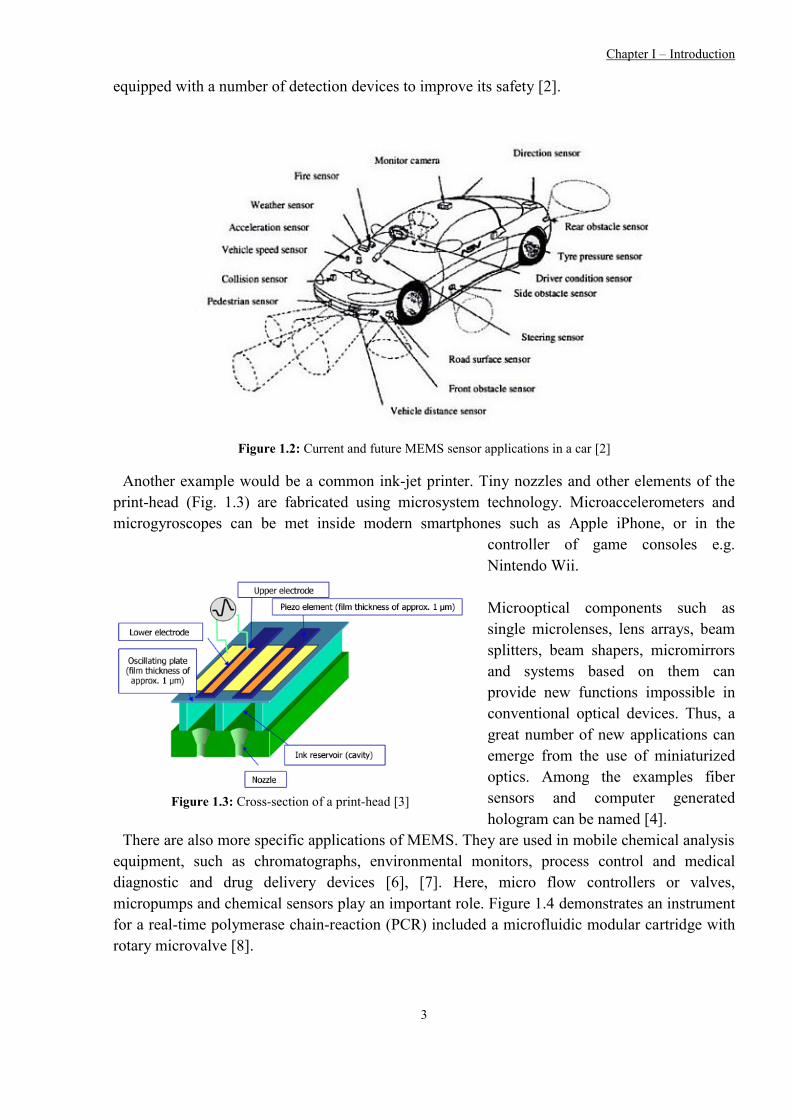
be given. For instance, the airbag control
system in a modern car begins with an
acceleration/deceleration sensor or
sensors and electronic circuits connected
to it (Fig. 1.1).
The number of microdevices in a car is
not restricted only with the above
mentioned acceleration/deceleration
sensor. Figure 1.2 illustrates the concept
of so called “advanced safety vehicle”
Figure 1.1: Airbag control system (left) and acceleration
sensor in a package (right) [5]
Chapter I – Introduction
3
equipped with a number of detection devices to improve its safety [2].
Figure 1.2: Current and future MEMS sensor applications in a car [2]
Another example would be a common ink-jet printer. Tiny nozzles and other elements of the
print-head (Fig. 1.3) are fabricated using microsystem technology. Microaccelerometers and
microgyroscopes can be met inside modern smartphones such as Apple iPhone, or in the
controller of game consoles e.g.
Nintendo Wii.
Microoptical components such as
single microlenses, lens arrays, beam
splitters, beam shapers, micromirrors
and systems based on them can
provide new functions impossible in
conventional optical devices. Thus, a
great number of new applications can
emerge from the use of miniaturized
optics. Among the examples fiber
sensors and computer generated
hologram can be named [4].
There are also more specific applications of MEMS. They are used in mobile chemical analysis
equipment, such as chromatographs, environmental monitors, process control and medical
diagnostic and drug delivery devices [6], [7]. Here, micro flow controllers or valves,
micropumps and chemical sensors play an important role. Figure 1.4 demonstrates an instrument
for a real-time polymerase chain-reaction (PCR) included a microfluidic modular cartridge with
rotary microvalve [8].
Figure 1.3: Cross-section of a print-head [3]

Chapter I – Introduction
4
Moreover, such systems are getting more and
more common in high frequency applications.
The most interesting examples in this area are
mechanical filters or resonators, microswitches,
varactors and inductors [9].
The first and the most obvious merit of
microsystems is their small size (normally from
1 µm to a few mm). This leads to smaller and
lighter devices, lower power consumption,
increase of production volumes and consequent
costs reduction. But miniaturization not only
saves place and space, but also brings other
advantages that broaden the borders of
applicability of different physical principles.
It is known, for example, that electrostatic
force between two charged particles is inversely
proportional to the square of the distance
between them. This makes it impossible to
design large systems based on the electrostatic
principle. On the contrary, microsystems widely
use this physical effect. Pressure sensors are
often built as variable capacitors that measure
the pressure applied to one of the plates
(diaphragm) by measuring the change in the
distance between the plates. The latter is inversely proportional to the capacitance. Thus, narrow
spacings must be used in order to receive reasonable output signal.
In medical, life science or chemical industry it is often necessary to analyze different chemical
compounds. Except of already mentioned compactness of such units based on MEMS, they
allow to use very small and precise amounts of chemicals for processing. This increases safety,
effectiveness and extremely reduces costs as there is no need in large chemical storage facilities.
Altogether, it results in greater product yield. Reduced volumes involved in the operations also
increase the speed of reactants dilution or injection.
The scope of this work is the design of technological process for the production of the
electrostatic curved beam actuator. Thus, it is necessary to pay more detailed attention to the
basics of microactuator fabrication processes and to the current state of technology of
microactuators and their applications.
1.2 Overview of the basic microfabrication techniques
In this subsection, a brief description of basic MEMS technologies and their relation to the
topic of this work is given.
Figure 1.4: The GeneExpert cartridge with a rotary
valve for sample preparation and real-time PCR [8]

Chapter I – Introduction
5
Normally, microactuator fabrication can involve a lot of MEMS bulk and surface
micromachining production techniques. Figure 1.5 shows examples of simple bulk and surface
micromachining sequences.
Figure 1.5: Bulk (left) and surface (right) micromachining sequences
Under bulk micromachining one understands processes where the body of the substrate
undergoes certain changes e.g. is being dry or wet etched, while surface micromachining means
bringing and structuring a sequence of thin films (usually ~1 µm) on the surface of a substrate.
In a nutshell, a standard MEMS fabrication process can be subdivided into the following steps:
1. substrate production
2. thin film deposition
3. photolithography
4. surface modification
5. etching
6. packaging
Step 1 refers to a fabrication of a substrate, on which the following processes will be carried
out. Steps from 2 to 5 usually repeat themselves several times in the whole fabrication process in
different combinations and sequences. Step 6 implies a block of final operations, to prepare the
fabricated system for characterization, delivery and utilization. In this work, thin film deposition
(electroplating, sputtering, CVD), photolithography, etching and surface micromachining play
the main role.
It is worth noting that although many microfabrication techniques came to MEMS production
from IC industry, there are a lot of other processes and materials that have been developed
exclusively for MEMS microfabrication. Table 1.1 represents this differentiation.

Chapter I – Introduction
6
Table 1.1 IC and MEMS Processes and materials
Conventional IC MEMS
Processes - photolithography,
- thermal oxidation,
- ion implantation,
- LPCVD,
- PECVD,
- evaporation,
- sputtering,
- wet etching,
- plasma etching,
- RIE,
- ion milling
- anisotropic wet
etching of single-
crystal silicon,
- DRIE,
- x-ray lithography,
electroplating,
- low-stress LPCVD
films,
- thick-film resist
(SU-8),
- spray-coating,
- micromolding,
- batch
microassembly
Materials silicon, silicon dioxide, silicon
nitride, aluminum
Piezoelectric films (PZT),
magnetic films (Ni, Fe, Co),
high temperature materials
and ceramics, aluminum
alloys, stainless steel, Pt, Au,
sheet glass, PVC, PDMS
The main processes used in fabrication of a curved beam electrostatic microactuator will be
described in detail in chapter 3 of this work.
1.3 Overview of Microactuators
This section is dedicated to the definition and classification of microactuators followed by
discussion of several examples that have been developed in last decades focused on the
technological fabrication processes and valve performance. Finally, technical specifications for
an electrostatically-actuated microvalve developed in this work will be introduced and a brief
description of the microvalve will be given.
1.3.1 Definition and classification
Microactuators have been in development since 1960s. The first examples would be an
electrostatic resonant-gate transistor, developed by Nathanson at RCA and a miniature
electromechanical resonator inside “Accutron” watch by “Bulova” Corp. [10], [11].
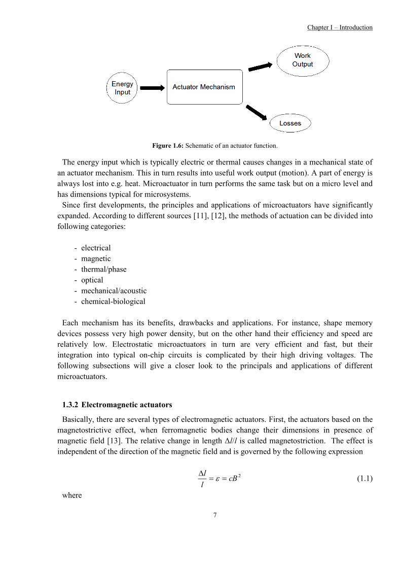
An actuator in general is a mechanical device for moving or controlling (i.e. actuating) a
mechanism or system in response to a control signal [12]. In other words, an actuator is an
energy transducer that transforms energy from one form into another (Fig 1.6).
Chapter I – Introduction
7
Figure 1.6: Schematic of an actuator function.
The energy input which is typically electric or thermal causes changes in a mechanical state of
an actuator mechanism. This in turn results into useful work output (motion). A part of energy is
always lost into e.g. heat. Microactuator in turn performs the same task but on a micro level and
has dimensions typical for microsystems.
Since first developments, the principles and applications of microactuators have significantly
expanded. According to different sources [11], [12], the methods of actuation can be divided into
following categories:
- electrical
- magnetic
- thermal/phase
- optical
- mechanical/acoustic
- chemical-biological
Each mechanism has its benefits, drawbacks and applications. For instance, shape memory
devices possess very high power density, but on the other hand their efficiency and speed are
relatively low. Electrostatic microactuators in turn are very efficient and fast, but their
integration into typical on-chip circuits is complicated by their high driving voltages. The
following subsections will give a closer look to the principals and applications of different
microactuators.
1.3.2 Electromagnetic actuators
Basically, there are several types of electromagnetic actuators. First, the actuators based on the
magnetostrictive effect, when ferromagnetic bodies change their dimensions in presence of
magnetic field [13]. The relative change in length Δl/l is called magnetostriction. The effect is
independent of the direction of the magnetic field and is governed by the following expression
2cBl
l
(1.1)
where

Chapter I – Introduction
8
ε – static strain produced by flux density B
c – material constant, [m4Wb
-2]
This effect is widely used in the design of ultrasonic devices, e.g. medical surgery instruments.
In MEMS, magnetostrictive films deposited by sputtering present a good actuation option in case
when contactless, high-frequency operation is needed, e.g. in noncontact torque sensing [14].
Another approach utilizes Lorentz force that acts on a current-carrying conductor in a magnetic
field making it move [15]. The Lorentz force law defines this force as
][ BqF (1.2)
where
q – electrical charge of the particle
ν – velocity of the particle
B – magnetic field
Magnetic actuation is favorable for its ability to generate relatively large forces and deflections
with low driving voltages. The drawback here is that scaling in the micro-domain is limited due
to the fact that electromagnetic force is directly proportional to the characteristic dimension as
F~D3. That means that a size reduction of 10 causes a magnetic force reduction of 10000.
Finally, there are actuators directly using magnetic attraction forces of permanent magnets. In
this case, scaling results appear to be one order of magnitude better [14].
It is obvious that presence of magnetic field is mandatory for all types of electromagnetic
actuators. Thus, utilization of magnetic materials is needed. The vast majority of the magnetic
actuators developed so far utilize soft magnetic materials like Ni0.8Fe0.2, which can be relatively
easy deposited by electroplating. Unfortunately, hard magnetic materials cannot be deposited
using standard MEMS technological solutions. However, they are still desirable in
electromagnetic microactuators because of good scaling properties and potential for larger forces
and deflections [16].
1.3.3 Electrostatic actuators
Electrostatic actuation has long been one of the most favorable choices in many MEMS
applications such as microvalves, tunable RF capacitors, microswitches or micromotors due to
its good scalability, low current consumption and relatively simple producibility. The reason for
it is the fact that electrostatic force Fel between two charged conductors increases as the distance
d between them decreases
2
2
0
,2d
wLUF r
zel
(1.3)
where

Chapter I – Introduction
9
εr – relative permittivity
ε0 – permttivity of vacuum
w – conductors width
L – conductors length
U – applied voltage
An example of such a design can be a vertically driven resonant microstructure.
On the other hand, the movement of charged plates can be realized parallel relative to each
other. In this case,
d
wUF r
xel2
2
0
,
and
d
LUF r
yel2
2
0
,
(1.4)
This approach allows larger displacements. Comb-drive actuators and rotary driven
electrostatic micromotors are the most obvious examples here.
Electrostatic actuation is a solution in cases of low force and energy densities. However, small
displacement requirement can turn from advantage into a disadvantage because it is a limiting
factor in some applications. For example, in microvalves, flow rates will be limited by smaller
gaps. Significant pressures cannot be withstood either. Further, the applied voltages are limited
by disruptive strength of the isolation layers. Electrostatic actuators are also very sensitive to
particles that can impede the motion of the moving parts. Moreover, these particles can lead to
sparkovers.
In this work, alternative curved-beam design is presented. It implements one stationary flat
electrode and a movable electrode in a shape of a curved cantilever beam. Due to this layout,
better balance between force and displacement can be achieved1.
1.3.4 Piezoelectric actuators
Piezoelectric (PZT) actuators utilize the effect of a mechanical stress appearance in certain
crystals under an applied electrical field. In a simplified way, the effect can be described by
noting the anions and cations moving in opposite directions under the influence of an electric
field. This leads to forces generation which in turn causes lattice deformation in
noncentrosymmetric crystals due to the presence of both high and low-stiffness ionic bonds
[14].
Going deeper in the theory of piezoelectricity would require an understanding of the
piezoelectric equations describing the coupling between mechanical and electrical strains in a
piezoelectric material.
If a stress σ is applied to a piece of piezoelectric material (e.g. quartz) the resulting one-
dimensional strain ε will obey the Hooke’s law
1 More detailed description of the theoretical principles is given in Chapter 2 of this work

Chapter I – Introduction
10
S (1.5)
where S = E-1
is the compliance, and E is Young’s modulus.
Further on, if a potential difference is applied across the faces of the material, an electric field E
appears and one can write
PED 0 (1.6)
where
D – electric displacement (electric flux density)
ε0 – permittivity of vacuum
P – polarization (electric dipole moment per unit of material)
Equation 1.5 contains only mechanical parameters while equation 1.6 only electrical ones.
These equations can be combined into equations both for direct and inverse piezoelectric effects.
In case of actuation, only the latter is of interest
ESdE (1.7)
DSgD (1.8)
where
d and g – piezoelectric constants in mV-1
and mC-1
respectively
SE – the compliance at constant field
SD – the compliance at constant electric flux density
Solving equations 1.7 and 1.8 for σ gives
E
YEeE )( (1.9)
D
YEhD )( (1.10)
where
e = d/SE and h = g/S
D – piezoelectric constants
E(Y)E – the Young’s modulus under constant electric field
E(Y)D – the Young’s modulus under constant electric flux density
Another important parameter is the electromechanical coupling coefficient k, which is a
measure of the interchange of electrical and mechanical energy
Chapter I – Introduction
11
gek (1.11)
Large forces (up to several MPa) can be generated using PZT actuation. Among the other
advantages based on the example of PZT micromotor and summarized in [14] are high energy
densities and low driving voltages.
However, generated displacements are relatively small. The latter can be overcome by utilizing
bi-morph film or stack design (Fig. 1.11c). Another disadvantage is limited miniaturization
opportunity due to the falling-off of the piezoelectric effect with the bulk of the material [14].
1.3.5 Thermal actuators
Thermal actuation occurs due to the property of materials to expand or contract as they undergo
temperature changes. These approaches are considerably useful when large forces accompanied
by large strokes are needed. Thermally actuated microsystems often possess relatively simple
design. However, they demonstrate slow response times, high power consumption and sensibility
to the ambient temperature conditions [10].
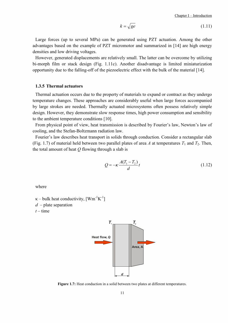
From physical point of view, heat transmission is described by Fourier’s law, Newton’s law of
cooling, and the Stefan-Boltzmann radiation law.
Fourier’s law describes heat transport in solids through conduction. Consider a rectangular slab
(Fig. 1.7) of material held between two parallel plates of area A at temperatures T1 and T2. Then,
the total amount of heat Q flowing through a slab is
td
TTAQ
)( 21 (1.12)
where
κ – bulk heat conductivity, [Wm-1
K-1
]
d – plate separation
t – time
Area, A
Heat flow, Q
d
T2T1
Figure 1.7: Heat conduction in a solid between two plates at different temperatures.

Chapter I – Introduction
12
Consequently, heat conduction or heat flux, q, is the heat flow per unit area and time, meaning
)( 21 TTdAt
(1.13)
or in more general form known as Fourier’s law of heat conduction
),(),( trTtrq (1.14)
where
r(x,y,z) – position vector in the heat conductor
T – temperature gradient
Newton’s law of cooling is a discrete analog of the Fourier’s law and describes heat transfer in
fluids through convection
)( 21 TThAq (1.15)
where
h – constant convective heat transfer coefficient, [Wm-2
K-1
]
A – surface area of the heat being transferred
It is worth noting that term “constant” with respect to heat transfer coefficient means that this
coefficient is temperature or rather temperature difference independent. This is the only case
when Newton’s law of cooling in this form is applicable to the description of convection heat
transfer.
As it has already been mentioned above, the radiation mode of heat transfer is governed by the
fundamental Stefan-Boltzmann law
4ATq (1.16)
where
T – absolute temperature
A – surface area
The constant of proportionality σ = 5,670400×10⁻⁸
Js-1
m-2
K-4
called the Stefan-Boltzmann
constant. It derives from other known constants of nature.

Chapter I – Introduction
13
As can be seen from Eq. 1.16, radiant heat transfer is proportional to the fourth power of the
absolute temperature, whereas in cases of conduction and convection it was linearly proportional
to temperature differences.
Equation 1.16 describes the radiation from the ideal emitter, or blackbody. In real situation,
bodies emit less energy and their thermal emission can be described by
4ATq (1.17)
where ε is the emissivity of the surface ranging from 0 to 1.
Thermal actuators can be realized as bimorph (e.g. bimetallic), thermopneumatic or shape
memory alloy based devices. A brief insight to each of the approaches is given in the following
subsections.
1.3.5.1 Bimorph actuators
Bimorph actuation scheme is one of the basic and widely used approaches. The principle is in
the utilization of two materials2 with distinct thermal expansion coefficients αL (CTE). The
materials must be bonded together. Hence, the structure is usually a sandwiched strip or
membrane as schematically illustrated in Fig. 1.8 [1].
Figure 1.8: Schematic representation of a bimorph actuation principle.
As temperature changes from the initial state, a bimorph cantilever or membrane will bend due
to incompatible CTEs. The structure will return to its initial state once the applied heat is
removed.
One of the basic advantages of bimorph actuators is their nearly linear deflection vs. applied
power behavior. Unfortunately, these devices require high power for operation and have low
2 Very often, metals are used as the materials for bimorph actuators. Thus, term “bimetal” and “bimetallic” can be
met in literature.
Chapter I – Introduction
14
bandwidth determined mainly by thermal time constants [17]. However, they remain a popular
choice for many MEMS application, such as microvalves and micropumps.
1.3.5.2 Thermopneumatic actuators
Thermopneumatic actuators are relatively popular in MEMS due to their ability to deliver large
forces through long strokes [15]. Constructively, they consist of a sealed cavity filled with fluid
media. The media expands and evaporates upon heating thus, raising the pressure inside the
cavity. This, in turn, makes one of the cavity walls used as flexible element bulge outward.
Schematic representation of this principle is shown in Figure 1.11e.
1.3.5.3 Shape memory alloy actuators
Some metal alloys (e.g. NiTi, NiTiPd), after plastic deformation, return to their original shape
after being heated. This effect is called “thermal shape memory” or simply “shape memory” and
occurs due to a crystalline phase change known as “thermoelastic martensitic transformation”
[49] when a temperature-dependent phase transition between martensite and austensite phases of
the alloy takes place. The metal alloys having this capability are called shape memory alloys
(SMA). Large forces are achievable here, which makes this phenomenon a good choice for
actuation. But acting speeds are much lower than in case of electrostatic or piezoelectric devices.
Another possible demerit of SMA actuators is the need of mechanical biasing structures such as
springs to generate a return force, enabling cyclical behavior.
1.3.6 Optical actuators
Optical actuation means transformation of the photonic energy of incident light into mechanical
motion. This can be achieved by using photovoltaic effect to generate first voltage and/or
electrical current that will in turn power a mechanical part of such a system, e.g. motor,
piezoelectric or any other electrically driven actuator. However, such a design seems to be
neither sufficiently small nor effective. Fortunately, another solution exists. In the heart of it,
there are materials which exhibit the so called “photostriction effect”. Photostriction is the
generation of strain by irradiation of light. In a nutshell, this effect is a superposition of the
photovoltaic and the piezoelectric effects. Working schema will look very similar to what is
depicted in Figure 1.7 for a bimorph actuator. Only heating must be replaced with incident light.
Photostriction is rare. It can be met in certain ceramic materials. The most widely if not the
only one used material at the moment3 is lanthanum-modified lead zirconate titanate PLZT [18].
PLZT is an artificial ceramics made of Lead, Lanthanum, Zirconium and Titanium. Among the
other ceramics being investigated are PMN-PT doped with Tungsten and PZN-PT.
Until not, not very many research has been carried out on this very promising field. However,
several applications such as photo-driven relay, microwalking device have already been
demonstrated [19].
3 To the authors best knowledge.

Chapter I – Introduction
15
1.3.7 Biological actuators
Apart of those created by humans, there are microactuators created by nature itself. In fact, they
belong to the most versatile and efficient at all. Although they have limited lifetime and require
sometimes very specific environmental conditions, they offer a great diversity of functions, low
cost, self-assembly and nanoscale size to name a few.
There are three main types of biological actuators [17]:
- cytoskeleton/microtubules
- cilia/flagella
- muscle
Cytoskeleton is a framework of the cell. It is present in all cells and is very dynamic. Its main
function is to adapt the shape of a cell to the external conditions, provide movements of the
whole cell, intra and intercellular transport, cellular division etc. Microtubules in turn are one of
the active matter components of the cytoskeleton. They have a diameter of 25 nm and serve as
structural cell components and are involved in many processes within the cell including e.g.
mitosis, cytokinesis and others. Microtubules are self-assembled polymers of α- and β-tubulin.
Many intracellular components are transported within cells not by diffusion but by movement
along microtubules.
Cilia and flagella are thin cylindrical structures found in most microorganisms and animals,
but not in higher plants. Their function is to move (propel) cells or to transport substances
relative to them, for example, moving mucus along the respiratory passages, or making
spermatozoids move in the direction . Flagella are typically longer than cilia and their movement
is generated in a different way. However, their structures are very identical. They consist of a
bundle of microtubules surrounded by an extension of the cell’s membrane. Motion of cilia and
flagella is created by the microtubules sliding past one another. This requires motor molecules of
dynein, which link adjacent microtubules together, and the energy of adenosine triphosphate
(ATP). Dynein powers the sliding of the microtubules against one another — first on one side,
then on the other.
Muscle is a contractive tissue of higher animals, where specialized cells group together to
generate force and motion. Muscles are classified as skeletal, smooth and cardiac ones. Skeletal
muscles can be well voluntary controlled, whereas cardiac and smooth muscle contraction occurs
without conscious thought. Muscle cells contain contractive filaments that move past each other
and change the size of the cell. ATP is used for “fuel”. The two key molecules involved in the
muscle actuation process are actin and myosin. Myosin generates traction along fixed actin
filaments using its head. Moreover, many myosin molecules can form bands that fit in between
actin filaments. The contraction of muscle is controlled by the release of Ca+ ions into the muscle
fibers.
Up to now it is still too early to speak of the applications of biological actuators in
micromachining. Still, they can potentially bridge the gap between micron-scale and nanoscale
structures, and their unique properties such as self-assembly can also bring the technology to a
new level of reliability and reproducibility.

Chapter I – Introduction
16
1.3.8 Applications of microactuators. Future trends.
While laboratory developments of almost all of the above mentioned types of microactuators
have been successfully demonstrated, their broad commercialization has been more difficult [9].
Nevertheless, there are examples of successful commercial introduction of microactuators, such
as piezoelectric microactuators used in ink-jet printer heads [20]. In biomedicine, SMA and PZT
microactuators are used as micromanipulators or microgrippers (Fig. 1.9) and microscalpels [21].
Figure 1.9: Surgical SMA microgripper [21]
There is a growing interest in introduction of chemical microactuators in such spectacular
fields as microturbomachinery and microcombustion engines for aero-space applications [9].
Other promising applications of microactuators include micromotors, controllers of micromirrors
and other optical elements, micropumps and microvalves. These complex devices in turn can be
used in biomedicine, automotive aerospace and other fields of application.
In the nearest future it is likely to expect more interest and research in the fields of so called
“smart” actuators, i.e. those that are based on smart materials and structures that capable to
return both sensing and actuating functions (e.g. piezoelectric and converse piezoelectric effects)
[19]. A lot of work towards development of biomechanical microactuators is also being carried
out.
A detailed review of each microactuators application field lies beyond the scope of this work.
However, it is still necessary and interesting to take a deeper look into at least one of them. This
will give an understanding of practical microactuators utilization, current developments and
trends. In the following subsections, applications of microactuators in microvalves are described.

Chapter I – Introduction
17
1.4 Microvalves: basic information
Over the last decades, microfluidic systems and microvalves in particular have become
indispensable in automotive, aerospace, healthcare and many other applications. However, in
spite of great number of research and development in this field, microfluidic components are still
far from wide commercialization [7]. High flow rates, switching speeds, operation stability and
low costs are the basic requirements to be met during the design and manufacturing of
microvalves and their components. These requirements are hard to be met all at once. Thus,
further research in this direction appears to be important in order to find the most efficient
technical solutions.
A microvalve can be defined as is a MEMS device that controls the flow of a fluid (gas, liquid)
by changing its volume, speed or direction. Typically, this function is implemented with the help
of a movable element (membrane, beam, or ball) that opens or closes a channel through which a
fluid flows. However, there are other principles of microvalve operation, such as for example,
rheological one, that does not necessarily include a mechanical component.
There are two main classes of microvalves: active and passive. Both classes include mechanical
and non-mechanical actuation principles. Passive microvalves do not require power for
actuation. The vast majority of them are so-called mechanical check valves. Check valves are
designed in such a manner that they only allow a fluid to flow in one direction and block it in the
opposite one. An example of a check valve design is represented in Fig. 1.10.
Figure 1.10: Check valve concept [22]
Non-mechanical passive microvalves include different capillary mechanisms. These devices
as well as non-mechanical active microvalves are beyond the scope of this work and will not be
discussed here. Detailed classification and overview of such systems is given in [7]. Further,
only examples of active mechanical microvalves will be presented since they are closely related
to the topic of this dissertation. Figure 1.11 schematically illustrates the basic actuation
principles of such microvalves.

Chapter I – Introduction
18
Figure 1.11: Actuation principles of active mechanical microvalves: (a) electromagnetic; (b) electrostatic;
(c) piezoelectric; (d) bimetallic; (e) thermopneumatic and (f) shape-memory alloy actuation [7]
Active mechanical microvalves can be further classified by their operational mode as normally-
open and normally closed. The former one lets the fluid flow pass through the valve when no
power is applied to it, whereas the latter on the contrary blocks the flow under the same
condition.
1.4.1 Electromagnetic microvalves
Possibly the first ever produced microvalve was an injection valve in a gas chromatographic
analyzer introduced by Terry et al.. in 1979 [23]. In this device, an electromagnetic actuation
principle was realized with a solenoid plunger (Fig. 1.12).
Figure 1.12: The microvalve with a solenoid plunger by Terry et al. [23]

Chapter I – Introduction
19
The valve was fabricated on a 2-inch silicon wafer. Anisotropic KOH silicon etching
techniques were used in order to form the through holes, the valve cylinder and the seating rings.
Solenoid was fabricated separately and then connected to the valve body by threading.
Since then, multiple different electromagnetically actuated microvalves using external magnetic
fields have been reported [7]. One of the biggest technological disadvantages of this method is
relative complexity of assembles. Magnets or solenoids must be somehow connected to the
device after fabrication. This makes batch production difficult if not impossible and also
complicates miniaturization. There are however integrated magnetic inductors fabricated using
MEMS-based technology [7]. Figure 1.13 demonstrates such assemble realized utilizing a low-
temperature biochemically compatible polymer bonding process [24]. This assemble consists of
three main parts: glass motherboard, structured with bulk micromachining etching techniques,
glass spacer substrate with etched through-holes, and a silicon-based active microvalve element
with silicon membrane, also structured by etching.
Figure 1.13: Magnetic microvalve with an integrated magnetic inductor by Oh et al. [24]
Large strokes are among the benefits of this approach, both with external or integrated
inductors [25]. Flow rates up to 1300 ml/min at operating current of 1A and differential
pressures of more than 200 kPa were achieved by Oh et al. [24]. Moderate response time from 3
ms to 10 ms is usually demonstrated by electromagnetic microvalves [26].
1.4.2 Electrostatic microvalves
Electrostatically actuated microvalves have been in active development since 1990 when such
design was introduced by Ohnstein et al. [27]. Such devices have been basically used in
pneumatic applications. They possess high efficiency, offer high switching speeds and have little
dependence on the ambient temperature. However, due to the nature of the electrostatic force
their driving voltages must be relatively high (up to more than 350 V) in order to withstand high
differential pressures. If high voltages are not achievable, electrostatic valves demonstrate
moderate performance in terms of pressure range and flow rates. Very often, silicon etching
techniques accompanied by metal deposition techniques are used in fabrication of electrostatic
valves. For example, relative majority of electrostatic microvalve designs use membranes of
different shape and material as an active element. Yang et al. [28] reported an electrostatically
driven microvalve with measured flow rate of 45 ml/min at room temperature with operating
voltage of 136 V. A silicon membrane was used as its active element. The valve has a
comparatively complicated design (Fig. 1.14).
Chapter I – Introduction
20
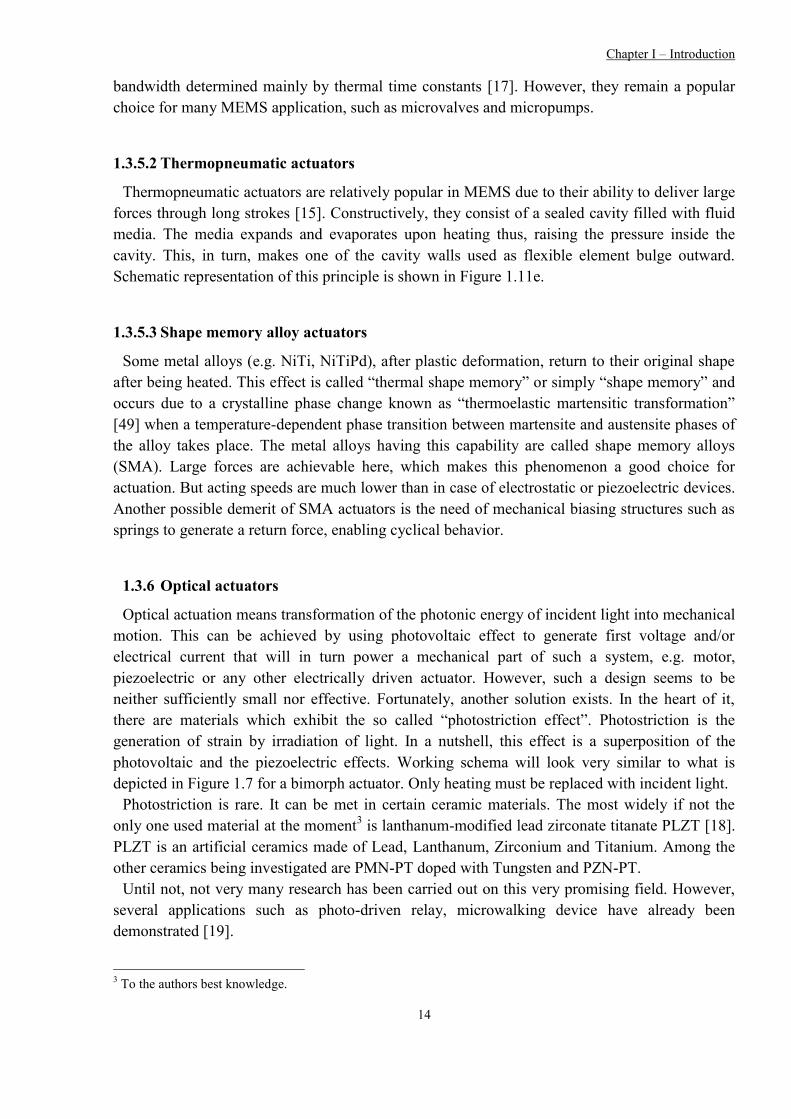
Figure 1.14: Electrostatic fuel valve [28]
Fabrication included direct bonding of multiple silicon-on-insulator (SOI) wafers, deep-reactive
ion etch (DRIE) as well as different thin-film deposition and structuring techniques.
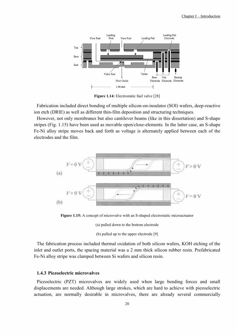
However, not only membranes but also cantilever beams (like in this dissertation) and S-shape
stripes (Fig. 1.15) have been used as movable open/close-elements. In the latter case, an S-shape
Fe-Ni alloy stripe moves back and forth as voltage is alternately applied between each of the
electrodes and the film.
Figure 1.15: A concept of microvalve with an S-shaped electrostatic microactuator
(a) pulled down to the bottom electrode
(b) pulled up to the upper electrode [9]
The fabrication process included thermal oxidation of both silicon wafers, KOH etching of the
inlet and outlet ports, the spacing material was a 2 mm thick silicon rubber resin. Prefabricated
Fe-Ni alloy stripe was clamped between Si wafers and silicon resin.
1.4.3 Piezoelectric microvalves
Piezoelectric (PZT) microvalves are widely used when large bending forces and small
displacements are needed. Although large strokes, which are hard to achieve with piezoelectric
actuation, are normally desirable in microvalves, there are already several commercially

Chapter I – Introduction
21
available designs of such systems [7]. The inability to perform large displacements has been
successfully overcome by different design approaches, e.g. stacked piezoelectric disks, or
hydraulic amplification [7]. However, high voltages are usually needed to activate such a device.
A microvalve operated at 500 V with maximal flow rate of 12 ml/min was reported by Roberts et
al. in 2003 [29]. Rogge et al. [30] developed a normally closed microvalve with a 25-fold
hydraulic amplification achieving a valve stroke of 50 μm at driving voltages of up to 300 V with
a response time of 2 ms. Maximal flow rate of 70 ml/min was achieved by Shao et al. [31]. One
of the concepts of a piezoelectric microvalve with stacked PZT is shown on Fig. 1.16.
Figure 1.16: A concept of a piezoelectrically actuated microvalve with stacked PZT [26]
This valve was fabricated using two wafers: an SOI wafer with the device layer and a Pyrex
glass wafer with inlet and outlet ports created with an electrochemical discharge machining
process. SOI wafer was etched using DRIE techniques whereas glass wafer was wet etched.
Finally, both wafers were bonded together by the anodic bonding.
Another example of a piezoelectrically actuated microvalve with thin film PZT was
demonstrated on Fig 1.11 (c).
1.4.4 Thermally actuated microvalves
Thermally actuated microvalves utilize bimetallic, thermopneumatic and shape memory alloy
actuation principles.
1.4.4.1 Bimetallic microvalves
Bimetallic microvalves usually have a thin-film bi-layer of metals serving as heater-elements
deposited on the membrane. When heated (i.e. by electric current), these elements deform due to
the difference in thermal expansion coefficients, thereby deforming the membrane. Jerman [32]
reported a bimetallic microvalve with Al/Si membrane (Fig. 1.17) and measured flow rate of 150
ml/min at differential pressure of 350 kPa. A leakage flow rate of N2 gas was about 30 µl/min at
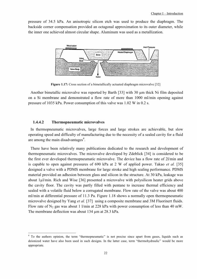
Chapter I – Introduction
22
pressure of 34.5 kPa. An anisotropic silicon etch was used to produce the diaphragm. The
backside corner compensation provided an octagonal approximation to its outer diameter, while
the inner one achieved almost circular shape. Aluminum was used as a metallization.
Figure 1.17: Cross section of a bimetallically actuated diaphragm microvalve [32]
Another bimetallic microvalve was reported by Barth [33] with 30 µm thick Ni film deposited
on a Si membrane and demonstrated a flow rate of more than 1000 ml/min opening against
pressure of 1035 kPa. Power consumption of this valve was 1.02 W in 0.2 s.
1.4.4.2 Thermopneumatic microvalves
In thermopneumatic microvalves, large forces and large strokes are achievable, but slow
operating speed and difficulty of manufacturing due to the necessity of a sealed cavity for a fluid
are among the main disadvantages4.
There have been relatively many publications dedicated to the research and development of
thermopneumatic microvalves. The microvalve developed by Zdeblick [34] is considered to be
the first ever developed thermopneumatic microvalve. The device has a flow rate of 2l/min and
is capable to open against pressures of 690 kPa at 2 W of applied power. Takao et al. [35]
designed a valve with a PDMS membrane for large stroke and high sealing performance. PDMS
material provided an adhesion between glass and silicon in the structure. At 30 kPa, leakage was
about 1µl/min. Rich and Wise [36] presented a microvalve with polysilicon heater grids above
the cavity floor. The cavity was partly filled with pentane to increase thermal efficiency and
sealed with a volatile fluid below a corrugated membrane. Flow rate of the valve was about 400
ml/min at differential pressure of 11.3 Pa. Figure 1.18 shows a normally open thermopneumatic
microvalve designed by Yang et al. [37] using a composite membrane and 3M Fluorinert fluids.
Flow rate of N2 gas was about 1 l/min at 228 kPa with power consumption of less than 40 mW.
The membrane deflection was about 134 µm at 28.3 kPa.
4 To the authors opinion, the term “thermopneumatic” is not precise since apart from gases, liquids such as
deionized water have also been used in such designs. In the latter case, term “thermohydraulic” would be more
appropriate.

Chapter I – Introduction
23
Figure 1.18: The thermopneumatic microvalve with composite
silicone rubber/Parylene membrane by Yang et al. [37]
1.4.4.3 Shape memory effect microvalves
Utilizing shape memory effect, microvalves can introduce high output forces enough to
withstand high differential pressures and flows [7]. Shape memory effect also allows compact
and simple structures. Among the disadvantages of the method are low efficiency and low
operational bandwidth (typically 1 -5 Hz), though operational frequencies up to 30 Hz have been
reported [7], [38].
An example and working principle of a normally closed SMA actuated microvalve is
demonstrated on Figure 1.19. An external metal spring keeps the valve closed when no heating is
applied to the SMA [33]. Once heated, the deformed SMA returns to its original shape thus
lifting the bossed valve membrane against the spring and opening the valve.
Figure 1.19: A normally closed SMA microvalve with external metal spring [33]
Kohl et al. presented different gas microvalves with SMA thin film [39]. NiTi, NiTiCu and
NiTiPd SMA were used for the actuation (Fig 1.20).

Chapter I – Introduction
24
Figure 1.20: Schematic cross-section of a thin film SMA microvalve [39]
A pressure chamber with inlet and outlet ports A and B was realized by mechanical
micromachining of a PMMA substrate. A polyimide membrane with lithographically structured
holes was integrated onto the pressure chamber by membrane transfer for a silicon substrate. The
SMA microdevice was interconnected to the cover by adhesive bonding. Flow rates of 360
ml/min at differential pressures below 260 kPa were achieved with stroke of about 20 µm at
power between 110 mW and 220 mW.
A miniaturized normally closed pinch-type microvalve was reported by Pemble and Towe [40].
It employed wires of NiTi SMA to control flows in Si tubing. A maximum flow rate of 16.8
ml/min at a differential pressure of 20.7 kPa with a power consumption of 298 mW was
permitted.
1.4.5 Microvalves on alternative principles
This brief overview of microvalves would not be complete without mentioning of several
different approaches to the realization of microvalves. Among them one can outline bistable
devices and microvalves utilizing different combinations of principles discussed above.
A common drawback of all the previously discussed typical active microvalves is that
continuous power must be applied in order to keep the device open in normally closed mode or
closed in normally open one. Bistable microvalves solve this problem since they only require
power to switch between two stable positions.
An interesting design that illustrates this approach was proposed by Fazal et al. [41]. A
miniature stepper motor mounted on a spring and a screw connected to its rotor to deflect the
membrane of the microvalve were used by this group (Fig. 1.21).

Chapter I – Introduction
25
Figure 1.21: A stepper-motor actuated microvalve [41]
This approach allows withstanding high pressures and does not require any power to maintain
any intermediate state of the system. Moreover, there is no interaction between a working fluid
and the actuation mechanism. The construction consists of two silicon wafers and one Pyrex
wafer bonded together. Standard micromachining techniques, such as KOH and DRIE etching
were used. Air flow rates of 220 ml/min at a pressure difference of 400 kPa were reported.
Another realization of a bistable microvalve using thermal buckling was presented by Goll et
al. [42]. Buckling of the polysilicon membrane with
a compressive stress was introduced by thermal
treatment and mechanical loading. The closed
microvalve could withstand inlet gas pressure up to
47 kPa. Bohm et al. [43] reported a bistable
electromagnetic microvalve using a NeFeB
permanent magnet, a 800-turn solenoid coil and a
spring biased armature to achieve bistable actuation
with a stroke of 200 µm (Fig. 1.22).
The application of the positive current to the coil
reduced the holding force of the armature with the
magnet and hence the spring could push the
armature downward to close the valve. A negative
current pulse would then open the valve again.
The valve consists of a micromachined and
conventionally machined bi-stable electromagnetic actuator parts connected together in one
assemble. The silicon valve part is a “sandwich” construction of two silicon wafers etched in
KOH. There is also a layer of chemical resistant silicon rubber bonded in between to provide the
flexibility needed to move the valve boss, as well as for improved sealing.
Additionally, combinations of the actuation mechanisms e.g. pneumatic-electrostatic or
electromagnetic-electrostatic are used to design bistable microvalves. A design proposed by
Bosch et al. [44] utilized the latter combination in a microvalve for gas flow regulation. It
incorporated a membrane part with an integrated planar coil, which was bonded to another part
defined as electrode. A membrane part was additionally placed between permanent magnets.
Figure 1.22: The bistable electromagnetic
microvalve with an integrated magnet [43]
Chapter I – Introduction
26
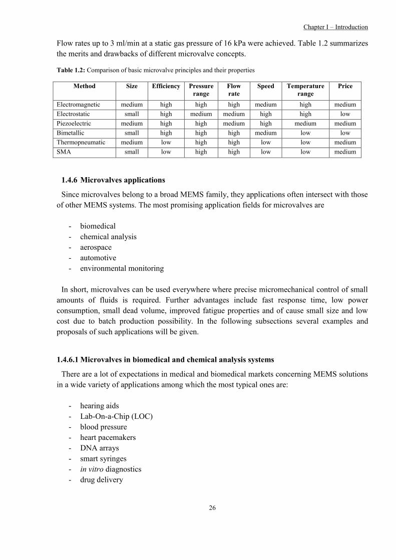
Flow rates up to 3 ml/min at a static gas pressure of 16 kPa were achieved. Table 1.2 summarizes
the merits and drawbacks of different microvalve concepts.
Table 1.2: Comparison of basic microvalve principles and their properties
Method Size Efficiency Pressure
range
Flow
rate
Speed Temperature
range
Price
Electromagnetic medium high high high medium high medium
Electrostatic small high medium medium high high low
Piezoelectric medium high high medium high medium medium
Bimetallic small high high high medium low low
Thermopneumatic medium low high high low low medium
SMA small low high high low low medium
1.4.6 Microvalves applications
Since microvalves belong to a broad MEMS family, they applications often intersect with those
of other MEMS systems. The most promising application fields for microvalves are
- biomedical
- chemical analysis
- aerospace
- automotive
- environmental monitoring
In short, microvalves can be used everywhere where precise micromechanical control of small
amounts of fluids is required. Further advantages include fast response time, low power
consumption, small dead volume, improved fatigue properties and of cause small size and low
cost due to batch production possibility. In the following subsections several examples and
proposals of such applications will be given.
1.4.6.1 Microvalves in biomedical and chemical analysis systems
There are a lot of expectations in medical and biomedical markets concerning MEMS solutions
in a wide variety of applications among which the most typical ones are:
- hearing aids
- Lab-On-a-Chip (LOC)
- blood pressure
- heart pacemakers
- DNA arrays
- smart syringes
- in vitro diagnostics
- drug delivery

Chapter I – Introduction
27
The biomedical applications of BioMEMS have been growing only for about last ten years. It is
also necessary to say that in comparison with automotive industry, where the market for
microsystems is already mature for broad commercial applications, the market for BioMEMS is
still in its development phase with chemical, flow and pressure sensors as its main driving forces.
However, as an integral part of BioMEMS, microvalves can be met both in therapeutic and
diagnostic systems. An example of therapeutic application would be drug and gene delivery
system. A diagnostic application is so called micro-total-analysis-systems (µTAS). Apart from
size and weight, biocompatibility and overall security of the device must be foreseen. Moreover,
if placed inside human body, the system must be controlled wirelessly and have an autonomous
energy source [45]. This makes the task of designing and producing such a microvalve more
complex.
A good example of commercially available microvalve for medical application would be a
thermopneumatic microvalve device produced by Redwood Microsystems (Fig. 1.23).
Figure 1.23: Thermopneumatic microvalve and its working principle (adapted from [15])
The performance of the device is reported to be comparable with macroscopic solenoid valves.
1.4.6.2 Aerospace applications of microvalves
Aerospace applications provide tremendous opportunities for different MEMS devices to be
incorporated in many systems. First of all, one speaks here of MEMS sensors and gyros.
However, there is also some place for microvalves. For example, in many cases sufficient and
effective cooling is required (prevention of telescope overheating in order to minimize the
infrared spectrum information distortion). In such systems microvalves can play a significant
role [26]. The valves can be distributed in an array of cooling elements (Fig. 1.24), which will be
placed across the structure to be cooled.

Chapter I – Introduction
28
Figure 1.24: A distributed cooling system concept [26]
The effective temperature controlling is achieved by independent work of each element in
response to the feedback from local sensors.
Since aerospace application requirements are extremely strict, mass, size and stable
performance in a wide range of temperatures and pressures of the valve become very critical.
1.4.6.3 Microvalves in automotive industry
A typical car has about 50 valves that need to be opened and closed automatically and regulated
closely [46]. Additionally, current trends to miniaturization and weight reduction could make
utilization of microvalves in automotive production very attractive. Microvalves can be used for
example in a car air-conditioning systems, or in micro-nozzle systems for fuel injection.
Until now however, to the author’s best knowledge, there are no commercially available
examples of microvalves built in a car.
1.4.6.4 Microvalves in environmental monitoring
MEMS are attractive in many environmental applications Micromachined devices are expected
to be in such areas as sensors for detection of air and water pollution and such instruments as gas
chromatography systems, microspectrometers and infrared detectors [15].
Miniature and accurate valves are good candidates to be used as sample injection-valves in
hand-held gas chromatography systems (GC), which are usually large and fragile. Two
companies have come up with commercially available bimetallic valves capable to be used in
hand-held GCs. The first one is Hewlett-Packard with its normally-closed Ni/Si-membrane-
valve, and the second one is IC Sensors with also normally-closed valve, but with aluminum
region on a Si-diaphragm (Fig. 1.17). The already mentioned thermopneumatic valve made by
Redwood Microsystems (Fig. 1.23) could also serve as a valve for GCs. However, it is thermally
inefficient due to large volume of working fluid, difficult to assembly, and quite slow (~400 ms).

Chapter I – Introduction
29
1.5 System and process specifications
The review of different microactuators and their applications given above clearly states the
main requirements to be normally met by these devices. In a nutshell, they are
- small size
- low energy consumption
- high robustness
- high stability
- application flexibility
- high switching speed
- high operating temperature range
- low costs
The technological process developed in this work should result in a microactuator with
following characteristics:
- actuation voltage: < 60 V
- switching speed: < 3 ms
- temperature range from: -10°C to +60°C
- working medium: gaseous (air, N2)
- chip size: 8 × 8 × 2.5 mm3
The process itself must incorporate mainly standard and easily achievable fabrication
techniques. Furthermore, the possibility of microactuator integration into different devices must
be foreseen in the process. For this work, a microvalve was chosen as a test-system for this task.
Though electrostatically actuated microvalves perform relatively poorly in terms of flow and
pressure ranges, the electrostatic actuation principle, it is still a favorable one since it allows high
switching speeds and small sizes at low costs. Apart of this, the characterization of technological
process and its electroplating part is one of the main objectives of this work. Electrostatically
actuated structures can be readily produced utilizing this method.
Finally, most of the electrostatically driven microvalves use parallel plate configuration of the
charged electrodes (one of which is integrated with movable membrane, or is a membrane by
itself). In this dissertation another approach is presented. A curved double-layer monometallic
beam serves as a movable open/close element (Fig 1.25).

Chapter I – Introduction
30
Figure 1.25: A general representation of a curved beam actuator for a microvalve.
This method allows increasing the gap between the electrodes thus, increasing the achievable
flow rates while actuation voltage can still remain low. In general, the minimal gap near the
anchor point as shown on Fig. 1.25 is mostly responsible for a minimal pull-in voltage. Should
this voltage be applied between the electrodes, the upper electrode i.e. curved beam will be
continuously attracted to the bottom one thus, closing the gap. On the other hand, since the gap
increases towards the free end of the beam, it also allows higher flow rates.
The concept described above was realized on silicon substrates using the methods of
microsystems manufacturing. A possibility of ceramic substrates utilization was also studied.
1.6 Structure of the dissertation
After the introduction, this work takes the reader through the Chapter 2 dedicated to the design
and development of the actuator (and microvalve). Theoretical questions regarding the actuator
micromechanics and fluid dynamics are discussed.
Chapter 3 describes the development of the technological process for microvalve fabrication.
Main attention will be paid to the microelectroplating process and dry etching methods as the
most critical ones in the fabrication chain. Technological process is presented. Also, the
possibility of ceramic substrates utilization was studied in Chapter 3.
Chapter 4 deals with the characterization of the actuator and the microvalve. The mechanical
robustness of the system is proved. This is necessary to assure that the fabrication process was
designed correctly. Several actuator and microvalve performance tests are also described in
Chapter 4.
Finally, in the Conclusion, all the work is summarized and possible directions and proposals for
future development are given.

Chapter II – Theory and design
31
2 Chapter II: Theory and design
In this chapter, theoretical aspects of the actuator design as well as design itself will be
discussed. First, definitions of electrostatic actuation, mechanical and electromechanical
behavior of the actuator followed by estimation of the related system parameters will be given.
Then, a brief theoretical description of flow behavior in a microvalve channel will be presented
and estimations of microvalve channel geometry will be discussed. In the conclusion, final
design variants will be presented.
2.1 Electrostatic actuation
Any design approach is based on a certain principle around which all the subsequent actions are
concentrated. In the present work this principle is the electrostatic interaction. The following
subsections describe nature of this phenomenon, the basics of electrostatic actuation, which will
in turn help to derive the design equations for the curved beam actuator.
2.1.1 Basics of electrostatic actuation
Electrostatic interaction is based on the Coulomb’s law, which states that the magnitude of the
electrostatics force of interaction between two point charges in vacuum is directly proportional to
the scalar multiplication of the magnitudes of charges and inversely proportional to the square of
the distances between them [47].
In scalar form, this statement is described by the following expression
2
21
r
qqkF eel
, (2.1)
where
q1 and q2 – point charges,
r – distance between two point charges,
ke – proportionality constant, or Coulomb’s constant which is related to the defined properties
of space
04
1
ek , (2.2)
where, in turn
ε0 – electric constant.
Figure 2.1 illustrates the mechanism of Coulomb’s law.

Chapter II – Theory and design
32
Figure 2.1: The mechanism of electrostatic interaction.
In vector form, the Coulomb’s law can be written as
12
12
2
12
2112
r
r
r
qqkF
(2.3)
where
r12 – distance between charge 1 and charge 2
12r
– vector from charge 1 to charge 2, equal in magnitude to r12
Obviously, the charges of the same sign are pushed away from each other, whereas the charges
which have different sign are pulling towards each other.
If there are more than two charges, the superposition principle may be used to determine the
force due to a system of N charges on a small test charge q
N
i i
ii
rr
rrqkqF
13
)(
(2.4)
For a charge distribution an integral over the region containing the charge is equivalent to an
infinite summation, treating each infinitesimal element of space as a point charge dq. Equations
2.5 – 2.7 represent the charge distribution per unit length, unit area, or unit volume respectively
')'( dlrdq (2.5)
')'( dArdq (2.6)
')'( dVrdq (2.7)

Chapter II – Theory and design
33
Here λ(r’) is the charge per unit length, σ(r’) is the charge per unit area, and ρ(r’) is the charge
per unit volume at position r’.
The force on an elementary charge q’ at the position r is then given by
dq
rr
rrkqF
3'
''
(2.8)
The phenomenon described above has practical meaning. When voltage U is applied, a parallel
plate capacitor can be seen as a system of charges of opposite polarity distributed over two
separated flat areas parallel to each other and separated by a distance d (Fig. 2.2).
Figure 2.2: Parallel plate capacitor.
The capacitance of this system is given by
d
AC el (2.9)
where
ε = ε0εr – permittivity, with ε0 – relative permittivity of the dielectric material between the
plates, and εr = 8.85×10⁻¹²
F/m – vacuum permittivity
Ael = wL – area of the plates, with w – plate width, L – plate length
The attracting force Fel will appear between these two plates. To derive this force, we can start
by writing the expression for the total potential energy of the capacitor
22
2
1
2
1U
d
ACUE el
pot (2.10)
The force between the plates is obtained by deriving Equation 2.10

Chapter II – Theory and design
34
2
22
1U
d
A
dd
dEF elpot
el (2.11)
If for example one plate remains fixed, and a counteracting force is somehow (e.g. spring)
applied to another one, the system may act as an actuator. This can be schematically represented
as:
Figure 2.3: Schematic of an electrostatic actuator.
As the distance between the plates is subject to change in this case so are the capacitance C and
consequently the force Fel (see Eq. 2.09 – 2.11). If d is the initial distance without any applied
voltage then after the voltage was applied, the upper plate will move to the position d – x, where
x is the displacement.
The spring will act in an opposite direction with force Fsp trying to restore the initial state of the
system. The force of the sprig is given by
kxFsp (2.12)
where k is the spring constant.
At equilibrium, Fel = Fsp, hence
2
2)(2
1U
xd
Akx el
(2.13)
It is now easy to find an expression for a pull-in voltage of a parallel plate electrostatic actuator,
for example as it is done in [48].
The total force acting on a movable plate is
kxUxd
AFFF el
speltot
2
2)(2
1 (2.14)

Chapter II – Theory and design
35
Deriving Equation 2.14 one obtains the stiffness of the system
kUxd
A
dx
dF eltot
2
3)( (2.15)
Substituting Eq. 2.13 returns stiffness around the equilibrium point
kxd
kx
dx
dFtot
2
(2.16)
The unstable point is defined by 0dx
dFtot resulting in
dx3
1 (2.17)
Substituting Eq. 2.17 to Eq. 2.13 gives the pull-in voltage of parallel plate electrostatic actuator
el
piA
kdU
3
27
8 (2.18)
The pull-in voltage turns out to depend on the actuators geometry and elastic properties of the
spring material as well as on the dielectric properties. Of cause, depending on application,
additional influencing parameters such as differential pressure (in case of a microvalve) can
contribute to pull-in voltage.
Often there is no separate spring attached to a movable plate. Instead, the plate itself acts as a
spring. This is true for cantilever beams and membranes. In this work, a bended cantilever beam
concept is used. The following subsection describes the theory behind the mechanical and
electrical properties of such a system.
2.1.2 Curved cantilever beam microactuator concept
Figure 2.4 schematically represents the basic mechanical concept of the prototype curved beam
electrostatic microactuator developed in this work. Consider a cantilever beam of length La
consisting of two layers of metal with thickness d1 and d2, internal stress σ1 and σ2, and Young’s
modulus E1 and E2. Suppose also that the properties of the material remain constant inside the
layer.

Chapter II – Theory and design
36
Figure 2.4: Microactuator mechanical concept [49]
In order to achieve the desired vertical deflection s at the tip of the actuator a single metal
double-layer approach was used. In this case, bending of a beam is caused by difference in
internal stresses inside these layers. The internal stress gradient appears due to variation of the
electroplating process parameters for each layer5. If there is a tensile stress inside one of the
layers whereas the other one has compressive stress, the beam will bend until the internal
bending forces become balanced. In equilibrium state the system will have certain bending
radius Rb. Knowing this radius, it is possible to geometrically estimate the deflection.
In Figure 2.5, the electrostatic working principal is shown
5 Discussed in Chapter 3 Technology and fabrication.

Chapter II – Theory and design
37
Figure 2.5: The electrical working principal of the curved beam electrostatic microatuator
The flat unmovable electrode is situated on the substrate and is electrically isolated from both
the movable electrode which is a curved cantilever beam and the substrate. The minimal distance
dmin between the electrodes is close to the anchor point of the cantilever beam. This distance
together with a number of other parameters defines the pull-in voltage Upi.
As Figure 2.5a shows, if there is no applied voltage or this voltage is lower than Upi the
actuator stays in its initial equilibrium position where its curvature is only defined by internal
stresses. However, as soon as applied voltage exceeds Upi the beam will bend towards the bottom
electrode until it lies almost completely flat on the isolation layer (Fig. 2.5b and 2.5c).
In order to define such design parameters as deflection s at any moment of time and pull-in
voltage Upi, it is necessary to define the geometry of the beam’s bending line w(x,U), which is
influenced on one hand by already mentioned internal stress gradient and on the other hand by
electrostatic forces acting on the beam [50]. This statement is illustrated in Figure 2.5
Figure 2.6: Actuators bending curve as a result of internal stress gradient and external electrostatic force

Chapter II – Theory and design
38
Thus, z0(x) is a bending line due to only internal stresses and zel(x,U) is a bending line due to
electrostatic force6. Their superposition gives the resulting bending line z(x,U)
),()(),( 0 UxzxzUxz el
(2.19)
Let us first determine the expression for a bending due to electrostatic force.
The bended beam and fixed electrode naturally form a capacitor with variable distance between
them along the X-axis. Therefore, it is necessary to subdivide all the length into elementary
discrete elements (capacitors) of length Δx and width w. Furthermore, the distance between the
electrodes dcap must be defined as
effcap dUxzUxd ),(),( (2.20)
with
j j
jiso
eff
dd
, , (2.21)
where
diso,j – thickness of the isolation layer j
εj – permittivity of the isolation layer j
The capacitance of the elementary capacitor considering Equation 2.10 will then be
xUxd
wUxC
cap
),(
),( , (2.22)
and consequently the electrostatic force between the plates of the elementary capacitor
),(
),(
2
1),( 2
Uxdd
UxdCUUxF
cap
cap (2.23)
Hence, dividing Equation 2.23 by Δx one receives electrostatic load per unit length
2
2),(2
1),( U
Uxd
wUxf
cap
el (2.24)
6 The latter is obviously also a function of a longtitudal distance x, since the gap between the electrodes changes as
well.

Chapter II – Theory and design
39
Now, taking into consideration the resulting load torque
L
x
elL dxUfUxM
)(),(),( (2.25)
and the differential equation for the bending line at small deflections as a function of the
bending strength cR
)(''))('1(
)(''
2xz
c
M
xz
xzel
R
L
el
el
(2.26)
one can get the final differential expression for the deflection caused by electrostatic force
combining the Equations 2.24, 2.25, and 2.26
L
x eleffR
el dUzzd
x
c
wUUxz
2
0
2
),()(
)(
)(
)(
2
1),('' (2.27)
Equation 2.27 is strongly nonlinear. It can only be solved numerically [50]. However, in most
cases it is only necessary to know the parameters at the initial and final position. These
parameters define for example the maximal deflection of the beam, which in turn can be used
during microvalve flow calculations if the actuator is used as a microvalve open/close element,
or on the other and, for definition of the necessary pull-in voltage. Initial bending of the beam is
only defined by its geometry and material properties. It will be derived in the following
subsections.
2.1.3 Beam bending radius and deflection
As it has already been mentioned in subsection 2.1.2, in the initial position, before pull-in
voltage is applied, the bending of the beam will only be caused by internal stress gradient due to
mechanical properties of the material and the geometry of the beam. This bending will stay
constant. Thus, the bending radius Rb will stay constant as well and can be defined as a
reciprocal of the second derivative of the bending line [50], [51]
);(),(
1
UxM
c
UxzR
L
Rb , (2.28)
or taking into considerations that no voltage is applied in the initial position
L
Rb
M
c
xzR
)(''
1 (2.29)

Chapter II – Theory and design
40
Now, the load torque ML and the bending strength cR must be defined. In order to do that, the
neutral axis of the multilayered beam should be found. According to the definition, “a neutral
axis is an axis in the cross section of the beam along which there are no longitudinal stresses and
strains” [52]. In the simplest case, i.e. the cross section is symmetric, isotropic and is not curved
before a bend occurs the neutral axis is a central axis of symmetry. The situation changes if the
body of a beam is not isotropic. For example, as in our case, it consists of several layers of
materials with different elastic properties.
Consider a beam of j layers as shown in Figure 2.7
Figure 2.7: Neutral axis in a beam of j layers
The position of the neutral axis depends on the width bj and on the Young’s modulus Ej of each
layer
1 2
1 1
1
2
1
1
0
2211
22
0
11
...
...
)()(
)()(
z z
z
z
z
jj
z
z
jj
z
z
z
z
zna
j
j
j
j
dzEbdzEbdzEb
zdzEbzdzEbzdzEb
dzzEzb
zdzzEzb
z (2.30)
We agree on the material parameters within the bulk of the layers to be constant. Moreover, the
widths are the same for all the layers and are constant. Thus, after integration, for a system of
two layers, the position of the neutral axis will be
2211
21
2
22
2
11 )2(
2
1
zEzE
zzzEzEzna
(2.31)
Now, it is possible to define the internal load torque ML responsible for the bending of the
beam, and the bending strength cR.
The internal load torque depends on mechanical stresses σj inside the corresponding layers.
Figure 2.8 depicts a system of j layers and internal stresses inside them. Negative values of σj are
for compressive stress, positive ones are for tensile stress.

Chapter II – Theory and design
41
Figure 2.8: Mechanical stresses inside a multilayered beam
There are two main reasons causing internal stress. First is a different process temperature
during the production of layers. Later on, when a system is situated under a certain common
temperature, different coefficients of thermal expansion will make it bend.
The second reason is connected to the material grain growth. Even if the same material is used,
on the border between two layers continuous grain growth is interrupted and the grains begin to
grow anew. Moreover, if different process parameters are used, grain size can differ from that in
the previous layer. Thus, stress gradient between the two layers appears [51].
As stated in [53], the internal load torque for a system of j layers is
1
1
2
10
2211 )(...)()())(()(
z z
z
najj
z
z
nana
z
naL
j
j
dzzzbdzzzbdzzzbdzzzzbzM (2.32)
After integration, and taking into consideration that the width b is the same for all the layers,
for a system of two layers, the internal torque will be defined as
nanaL zzzzzzzzbM 221
2
221
2
11 )2(2
1
2
1 (2.33)
The bending strength cR which also defines the spring’s elastic force can be found using the
following equation
dzzzEbdzzzEbdzzzEbdzzzzEzbcz
z
z
najj
z
z
na
z
nanaR
j
j
1
2
1
1
22
22
0
2
11
2 )(...)()())(()( (2.34)
Again, after integration for the system of two layers
2
221
2
22121
3
22
2
1
2
1
3
11 2)(33
1
3
1nanananaR zzzzzzzzzzzbEzzzzzbEc (2.35)
Using Equations 2.30, 2.34 and 2.36 one can find the static deflection of the bended beam due
to internal stress gradient st at its tip point. Considering the data from Figure 2.4 and the
approximation Rb >> La, after simple geometrical calculations [50], [51], one can write

Chapter II – Theory and design
42
R
faL
b
fa
b
fa
btc
lLM
R
lL
R
lLRs
2
)(
2
1cos1
22
, (2.36)
where
La – total length of the beam
lf – length of the flat part of the beam resting on the bottom electrode
Rb – beam bending radius
Similarly, deflection of the beam at any other point can be found by replacing the total length
Lb by the corresponding length of the beam at this point.
2.1.4 Beam pull-in voltage
Pull-in voltage Upi is one of the critical parameters to be defined during the design of the
actuator and represents the operational limits between stable and unstable behavior of an
electrostatic system. It is important to detain the beginning of the pull-in in order to achive better
performance of the device [54].
It is out of the scope of the present work to develop a high precision analytical model for a
curved cantilever beam. Such models exist [54], [55] and return excellent results, but they
require a huge number of mathematical calculations including usage of special mathematical
software to solve the systems of differential equations. Another approach based on FEM
simulations exist. This method is also a good one in case when high precision is needed. But due
to high complexity of the model7 and non-linear behavior of a curved beam, model generation
and meshing itself become very complex and time-consuming. Fringing effects [55] are not
considered in this work, either.
In the following, a simple model for estimation of a pull-in voltage for a given set of
parameters will be derived. The theoretical formulation is based on the models developed in
[50], [51], [54], [56].
Figure 2.4 represented the geometry of a curved cantilever beam. For such geometry, voltage
dependent tip deflection sel(U) can be defined as [56]
, (2.37)
where
k – effective dielectric constant, approximated value k = 1, 2046 [56]
st - static deflection of the bended beam due to internal stress gradient as in Eq. 2.36
7 A multiphysics problem: electrostatics and mechanics.

Chapter II – Theory and design
43
dsl – minimal gap between the curved beam and the isolation layer
I – moment of inertia
Eeff – effective Young’s modulus, Eeff = E/(1-ν2) for beams with b ≥ 5(z1+z2) [54]
ν – Poisson’s ratio
According to [48], pull-in occurs when
(2.38)
Taking into consideration Eq. 2.38 and solving 2.37 with respect to U returns
(2.39)
The definite integral in Eq. 2.39 can be represented as
, (2.40)
where
Rb – beam bending radius as in Eq. 2.29
Substituting the definite integral in Eq. 2.39 with Eq. 2.40 results in
(2.41)
2.1.5 Breakdown voltage
An important question during the design of any electrostatically actuated device is at what
voltage electrical breakdown will happen. In other words, when will the electrical arc take place?
This would define the highest voltages, which the device can withstand without damages.
To a certain extent, the answer to this question is given by Paschen’s Law. The law states that
the breakdown voltage UBD is a function of the product of the gas pressure p and the distance
between the electrodes d

Chapter II – Theory and design
44
Bpd
ApddpfU BD
)ln()( (2.42)
where
A and B – coefficients depending on the composition of the gas [57].
Figure 2.8 illustrates the curves for different gases.
Figure 2.9: Breakdown voltage vs. gas pressure [57]
It can be clearly seen that for high voltage applications the voltage gain on the left side of the
minimum can be used.
Paschen’s Law is only valid for electrodes with uniform electric field. Hence, it can only be
carefully applied in this work, where one of the electrodes is curved. Furthermore, its validity is
limited for small distances between the electrodes due to the fact that at high field strength,
collision ionization at the electrodes prevails [58]. This means that for the distances smaller then
several tenths of microns the dielectric strength of the electrodes gap cannot be improved by
decreasing gas pressure p [51].
2.1.6 Stiction phenomena and antistiction stand-off bumps.
Stiction (or sticking) is a phenomenon of adherence of two surfaces to each other. In case of
microstructures it can be adherence of an actuator beam to the surface of the bottom electrode, or
rather to the isolation layer covering this electrode.
Stiction is caused by solid-to-solid binding forces appearing when two flat surfaces are placed
very close to each other. These forces can be large enough to overcome the spring force of the
beam, which is responsible for returning it to the initial state after the voltage is turned off. In
this case the beam will stay in contact with bottom electrode and the device (valve or relay) will
not function. In surface micromachining stiction often first occurs after the wet etching of the
sacrificial layer when drying process is initiated. The structures undergo deflection due to

Chapter II – Theory and design
45
capillary forces caused by surface tension of the remaining liquid between microstructures.
Deflection decreases the gap between the structures and this in turn lets solid-to-solid forces pin
them together.
One possible solution could be additional force applied to the beam to tear it off the surface.
This solution is used in this work in a form of the prestressed actuator beam. Internal stress
gradient makes the beam bend upwards after the release etching, working against stiction forces.
Among the other methods are usage of structure supporting organic pillars, supercritical CO2
drying, and coating of structures with self-assembly monolayers (SAMs). Dry etching methods
are used to avoid stiction, but they do not guarantee that stiction will not appear later. There are,
however, other possibilities which are hidden in the design of the beam itself.
Stiction strength is directly proportional to the surface energy of the structures. Hence, by
decreasing the surface energy one can decrease stiction. The surface energy depends on the
material. For Ni it is quite high, about 2,34 J/m2 [59]
8. Ni was chosen as a material for the
actuator in this work for its good manufacturability and mechanical properties. Hence, this
solution cannot be used in this work.
Fortunately, the surface energy is also directly proportional to the total contact area [5].
Therefore, reduction of the total contact area will reduce stiction. This can be done by
incorporating small 15 µm ×15 µm stand-off bumps on the bottom surface of the beam. During
the operation, only these bumps will touch the isolation layer of the bottom electrode. The
concept is shown in Figure 2.10
Figure 2.10: Anti-stiction bumps on the bottom side of the actuator
The distance between the bumps is 195 µm. The big circular bump in the middle serves as a
valve boss for a microvalve application of the actuator. It can also be used as a contact bump in
for example relay application.
8 Compared to e.g. polycrystalline silicon (0,14±0,07 J/m2), or solidified gelatin (0,12±0,008 J/m
2) [5]
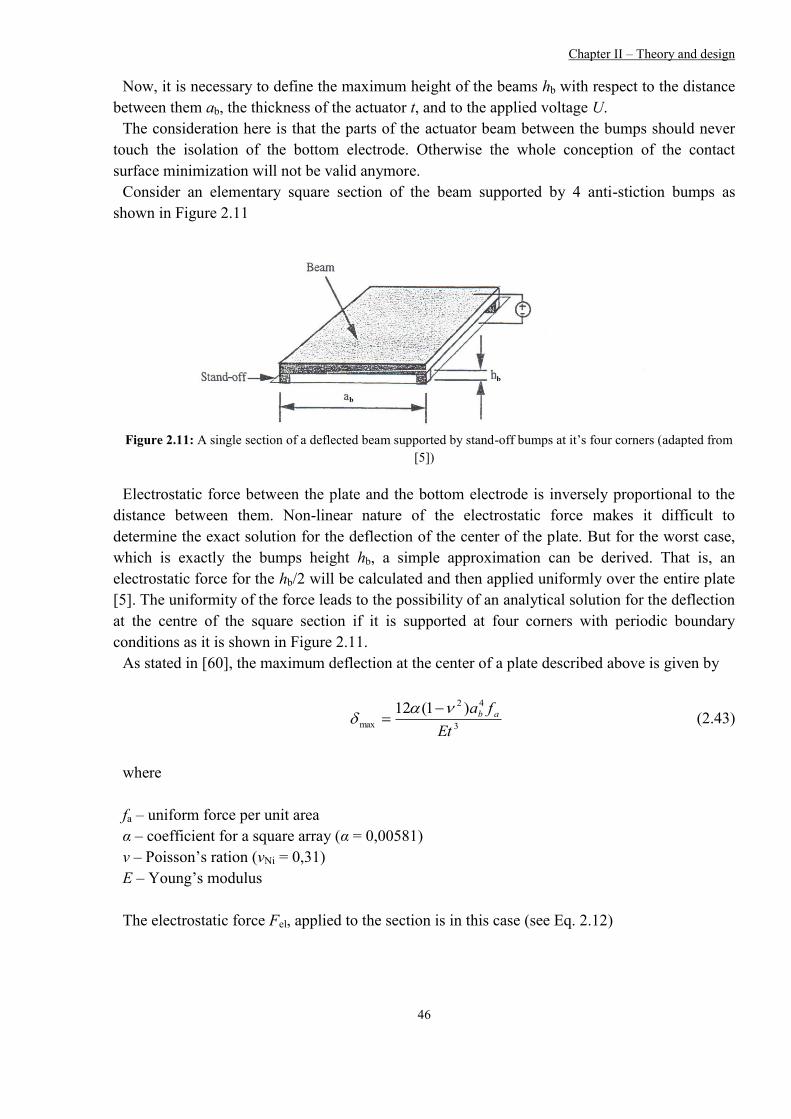
Chapter II – Theory and design
46
Now, it is necessary to define the maximum height of the beams hb with respect to the distance
between them ab, the thickness of the actuator t, and to the applied voltage U.
The consideration here is that the parts of the actuator beam between the bumps should never
touch the isolation of the bottom electrode. Otherwise the whole conception of the contact
surface minimization will not be valid anymore.
Consider an elementary square section of the beam supported by 4 anti-stiction bumps as
shown in Figure 2.11
Figure 2.11: A single section of a deflected beam supported by stand-off bumps at it’s four corners (adapted from
[5])
Electrostatic force between the plate and the bottom electrode is inversely proportional to the
distance between them. Non-linear nature of the electrostatic force makes it difficult to
determine the exact solution for the deflection of the center of the plate. But for the worst case,
which is exactly the bumps height hb, a simple approximation can be derived. That is, an
electrostatic force for the hb/2 will be calculated and then applied uniformly over the entire plate
[5]. The uniformity of the force leads to the possibility of an analytical solution for the deflection
at the centre of the square section if it is supported at four corners with periodic boundary
conditions as it is shown in Figure 2.11.
As stated in [60], the maximum deflection at the center of a plate described above is given by
3
42
max
)1(12
Et
fa ab
(2.43)
where
fa – uniform force per unit area
α – coefficient for a square array (α = 0,00581)
ν – Poisson’s ration (νNi = 0,31)
E – Young’s modulus
The electrostatic force Fel, applied to the section is in this case (see Eq. 2.12)

Chapter II – Theory and design
47
2
2
2
2
1U
h
AF
b
el
el
(2.44)
The force per unit area is defined as
2
2
22
bel
el
a
h
U
A
Ff
(2.45)
Substituting Equation 2.45 in Equation 2.43 returns
23
242
max
)1(24
b
b
hEt
Ua
(2.46)
Substituting hb/2 for maximum deflection and solving for hb yields
33
242 )1(48
Et
Uah bb
(2.47)
Equation 2.47 defines the minimum anti-stiction bump height. The maximum height can be
limited by a desired device parameter, e.g. maximum leak rate of the valve.
For given geometry, material properties of Ni and maximum applied voltage U = 60 V 9, hb ≥
200 nm.
2.1.7 Actuator reaction time
Very often, an operational speed of the device becomes an indispensible parameter. For
example, it is always important to know how fast a relay can switch, or how fast a valve can
open or close. The principle of the actuator’s movement is shown in the Figure 2.1210
.
The beam is assumed to be initially in an upward deflected state (Fig. 2.12 a). When the pull-in
voltage is applied, the beam simultaneously begins to uncurl and move downward to the bottom
electrode. When a portion of the beam reaches the height of approximately 1/3 of the dmin, the
beam will rapidly pull-down to the surface (Fig. 2.12 b and c). This pull-down time is neglected.
After the voltage is turned off, the beam will return to its initial state. Residual charges can make
this phase slower than closing phase. But in the presence of internal stress gradient contributing
to the restoring deflection, their influence can be neglected too.
9 Worst case as defined in specifications (see 1.5)
10 This is simply a copy of Figure 2.5 repeated here in order to make reading more comfortable.

Chapter II – Theory and design
48
Figure 2.12: Microactuator’s closing behavior
Maximum speed at which a cantilever beam can vibrate is defined by its undamped circular
frequency ω0 [61]
)(33
)(351
33
)(35
4
1
140
33
140
33
1
21
3
2
3
1
23
3
2
3
1
3
30
zz
zzE
LVL
zzbE
L
zbE
kc
Vmm
cm
eff
bb
eff
b
i
ieff
s
eff
eff
(2.48)
The undamped natural frequency is related with the circular frequency as:
2
0nf (2.49)
Knowing this frequency, one can easily estimate the time of one vibration cycle, or actuators
reaction time tr. Since the beam will only undergo one half of the complete cycle, we should take
only one half of this time, e.g.
n
rf
t2
(2.50)
This approach allows only an approximate estimation of the actuators closing speed. For more
precise calculations, damping and beam stiffness must be taken into consideration. In order to
reduce damping and also to provide better and faster sacrificial layer etching, the array of
technological through-beam orifices was foreseen.

Chapter II – Theory and design
49
2.1.8 Dimensioning of the actuator’s beam
Having derived all the necessary equations in previous subsections, one can calculate the
actuators mechanical and geometrical parameters. First of all, it is necessary to summarize and
classify the most important parameters (Table 2.1)
Table 2.1: Classification of basic parameters for actuator's dimensioning
Parameter Sign Type Value Comments
Width b Design
500…1500 µm Limited by chip dimensions
Length Lb 2500…4500 µm
Ni layer 1
thickness z1
Design/Process
0…2 µm Thickness of the microform
Ni layer 2
thickness z2 15…20 µm Thickness of the microform
Sacrificial layer
thickness dsl 0.2…1 µm -
Isolation layer
thickness diso 0.2…0.6 µm -
Ni layer 1 stress σ1 Process
-15..-30 MPa Limited by desired beam deflection
Ni layer 2 stress σ2 10..20 MPa
Ni Young's
modulus E Material 200 Gpa Material property
Pull in voltage Upi
Output
< 60 V Specifications, Eq. 2.42
Beam deflection st < 60 µm Eq. 2.37
Anti-stiction
bump height hb - To be calculated, Eq. 2.49
Switching time τmin < 3 ms Specifications, Eq. 2.54
The design parameters are freely11
defined by engineer and can be varied to achieve optimal
output parameters. Design/Process and process parameters have more limitations due to the
nature of technological processes involved here.
The main equations involved into the calculations are
Eq. 2.36 – static deflection st
Eq. 2.41 – pull-in votage Upi
Eq. 2.47 – stand-off bumps height hb
Eq. 2.50 – actuator’s reaction time tr
The stand-off bumps height hb was calculated in the subsection 2.1.6 and as should be not less
than 200 nm.
11
Can be varied in the limits of technical specifications

Chapter II – Theory and design
50
2.1.8.1 Static deflection
Static deflection due to internal stress gradient depends on design and design/process
parameters of the actuator. Figure 2.10 presents the dependence of static deflection on the length
of the actuator cantilever beam Lb at constant beam width b = 500 µm. Material and process
parameters were also set constant: E1 = E2 = E = 200 GPa, σ1 = 20 MPa, σ2 = -12 MPa, z1 = 2
µm, z2 = 18 µm
0,0
10,0
20,0
30,0
40,0
50,0
60,0
70,0
80,0
90,0
0 1000 2000 3000 4000 5000 6000 7000
Sta
tic
def
lect
ion
st,
[µm
]
Beam length Lb, [µm]
Figure 2.10: Static deflection of the double layered nickel actuator
Proper deflections of 10 to 40 µm can be achieved at lengths of 2000 to 4500 µm.
Mathematically, static deflection st does not depend on b, but depends on Lb, σ1/σ2 and z1/ z2.
Figure 2.11 illustrates some possible variations of st in dependence on the ratios z1/ z2 and σ1/σ2.
Here, Lb = 3000 µm and b = 500 µm.

Chapter II – Theory and design
51
0
10
20
30
40
50
60
70
80
90
0 1/5 2/5 3/5 4/5 1
Stat
ic d
efle
ctio
n s
t, [µ
m]
Layer thickness relation z1/z2
Sigma1=-20MPa,Sigma2=12MPa
Sigma1=-15MPa,Sigma2=15MPa
Sigma1=-25MPa,Sigma2=25MPa
Sigma1=-5MPa,Sigma2=5MPa
Sigma1=-20MPa,Sigma2=12MPa
Figure 2.11: Actuator static deflection vs. layer thickness ratio
Deflections of 10 to 25 µm can be achieved at the ratios of z1/ z2 from 1/5 to 1/1. Higher
deflections occur at higher values of internals stresses.
2.1.8.2 Pull-in voltage
The following graphs illustrate estimations of pull-in voltage Upi. First, dependence of pull-in
voltage on the length of the actuator Lb at constant width b = 500 µm and ratio z1/ z2 = 1/9 was
determined (Fig. 2.12).
Apart from obvious fact that higher internal stresses result in higher pull-in voltages, it is
interesting to mention that up to the length of approximately 500 µm pull-in voltage drops very
quickly but at lengths above 500 µm it again begins to slightly increase. And the higher the
internal stress is, the stronger is the increase in pull-in voltage. Pull-in voltage drop with
increasing actuator length was described in literature [54, 55]. But to the authors best knowledge
there was no investigation of the lengths above 1000 µm and the results derived in this
investigation can be useful for the future designs of the beams with comparable dimensions.
Furthermore, it was found that mathematically pull-in voltage does not depend on the width of
the actuator.

Chapter II – Theory and design
52
0
5
10
15
20
25
30
35
40
45
0 500 1000 1500 2000 2500 3000 3500 4000 4500 5000 5500 6000 6500
Pu
ll in
vo
ltag
e U
pi,
[V]
Beam length Lb, [µm]
Sigma1=-20MPa, Sigma2=12MPa
Sigma1=-15MPa, Sigma2=15MPa
Sigma1=-5MPa, Sigma2=5MPa
Figure 2.12: Pull-in voltage vs. actuator length
On the other hand, it was interesting to investigate the dependence of pull-in voltage on the
ratio z1/ z2. This dependence is depicted on Figure 2.13. The result is very similar to the one for
the static deflection. Again, with increasing internal stress, pull-in voltage increases. It also
increases as the ratio z1/ z2 increases.
0
5
10
15
20
25
30
0 1/5 2/5 3/5 4/5 1
Pu
ll in
vo
ltag
e, U
pi,
[V]
Layer thickness ratio z1/z2
Sigma1=-20MPa,Sigma2=12MPa
Sigma1=-15MPa,Sigma2=15MPa
Sigma1=-25MPa,Sigma2=25MPa
Sigma1=-5MPa,Sigma2=5MPa
Sigma1=-5MPa,Sigma2=25MPa
Figure 2.13: Pull-in voltage vs. layer thickness ratio. Lb = 3000 µm, b = 500 µm
Another parameter that influences pull-in voltage is the thickness of the sacrificial layer or the
minimal gap between the curved beam and the isolation layer dsl. Figure 2.14 illustrates this
dependence.

Chapter II – Theory and design
53
0
2
4
6
8
10
12
14
0,00 0,20 0,40 0,60 0,80 1,00 1,20
Pu
ll-in
vo
ltag
e U
pi, [
V]
Minimal gap dsl, [µm]
Figure 2.14:Pull-in voltage vs minimal gap. Lb = 3000 µm, b = 500 µm
At chosen design and design/process parameters, pull-in voltage is far below the specifications
limit of 60 V. This fact increases the flexibility in the dimensioning during the design of the
beam.
The next graphic (Fig. 2.15) can be used as an estimation tool to determine the pull-in voltage
at given geometry and design parameters. Here, Lb = 3000 µm, b = 500 µm, σ1 = -20 MPa, σ2 =
12 MPa, z1 = 2 µm and z2 = 18 µm.
0,00
20,00
40,00
60,00
80,00
100,00
120,00
140,00
160,00
180,00
200,00
0,00 10,00 20,00 30,00 40,00 50,00
Bea
m d
efle
ctio
n, [
µm
]
Voltage, [V]
Electrostatic deflection
Static deflection
Pot.(Electrostatic deflection)
Linear (Static deflection)
Figure 2.15: Graphical estimation of the pull-in voltage by static and electrostatic deflection
The parabolic curve depicts the deflection of the beam due to applied voltage. The horizontal
line is the constant deflection of the beam due to internal stress and geometry. At the point of

Chapter II – Theory and design
54
intersection the beam will be completely deflected to the surface. However, as it was mentioned
before, pull-in occurs at 1/3 of the complete deflection. Hence, in this example pull-in occurs at
deflection of about 7 µm that corresponds to approximately 10-11 V. The calculated (Eq. 2.41)
value for such a beam is 11,16 V.
2.1.8.3 Actuator’ reaction time
As follows out of the Eq. 2.49 – 2.51, the actuator’s reaction time tr depends on the beam’s
length Lb, layer thicknesses z1 and z2 and constant material properties. Therefore, the reaction
time was estimated as a function of length Lb and layer thickness ratio z1/z2 (Fig. 2.16).
0
2
4
6
8
10
12
14
16
18
20
0 1000 2000 3000 4000 5000 6000 7000
Rea
ctio
n t
ime
tr,
[ms]
Beam length Lb, [µm]
z1/z2=1/9
z1/z2=1/19
z1/z2=1/1
Figure 2.16: Actuators reaction time vs. beam length and layer thickness ratio
The reaction time does not depend on the beam’s width b. Obviously, it increases with
increasing beam’s length. The only parameter that could decrease the reaction time and can be
influenced by designer at chosen material is the ratio of the layer thicknesses. However, Fig. 2.16
demonstrates that this influence in the decrease direction is also very weak. Moreover, the
change of the ratio is limited by technological reasons and the fact that higher ratio also
decreases the beam’s deflection (Fig. 2.11). Thus, the ratio of z1/z2 = 1/9 was finally chosen.
2.1.8.4 Actuators dimensioning summary
In correspondence with the above discussed calculations the following fifteen actuator beam
design variants were proposed (Tab. 2.2)

Chapter II – Theory and design
55
Table 2.2: Actuator geometry design variations
Design ID Length Lb,
[µm] Width b,
[µm] σ1, [MPa] σ2, [MPa] z1, [µm] z2, [µm]
1.1 2500 850 -20 12 2 18
1.2 2500 600 -20 12 2 18
1.3 2500 500 -20 12 2 18
2.1 3000 1000 -20 12 2 18
2.2 3000 750 -20 12 2 18
2.3 3000 600 -20 12 2 18
3.1 3500 1200 -20 12 2 18
3.2 3500 900 -20 12 2 18
3.3 3500 700 -20 12 2 18
4.1 4000 1300 -20 12 2 18
4.2 4000 1000 -20 12 2 18
4.3 4000 800 -20 12 2 18
5.1 4500 1500 -20 12 2 18
5.2 4500 1100 -20 12 2 18
5.3 4500 900 -20 12 2 18
It was decided to keep the internal stresses σ1 and σ2 as well as the layer thicknesses z1 and z2
constant in order to avoid overwhelming process variations. Moreover, the calculations above
showed that at chosen values of stresses and thicknesses, specification limits should not be
violated. Instead, the geometry was greatly varied.
Longer beams would allow higher deflection that on the one hand would result in higher pull-in
voltages, but on the other hand are necessary for microvalve operation, which will be discussed
in the next subsections.
2.2 Microvalve design
In this subsection, basic fluid flow calculations regarding gas flow through microvalve are
presented. This is important since microvalves are thought to be one of the main applications of
the actuator being developed in this work. The aim of the calculations is to determine the
geometry and dimensions of the gas flow channel and the optimal position of the actuator above
the channel opening, i.e. the optimal valve lift at which the desired flow can be achieved.
2.2.1 Constitutive equations
The fluids in fluid mechanics are subdivided into compressible (gases) and incompressible
(liquids) ones. In this work, only the case of compressible fluids will be discussed, as the
working medium was chosen to be nitrogen (N2) or air.
The constitutive equations can be classified as thermal and isentropic [62]. The main thermal
equation for the ideal gas is
Chapter II – Theory and design
56
TRP S (2.51)
where
P – gas pressure
ρ – gas density
RS = R/M – specific gas constant with R – molar gas constant, and M – gas molar mass
T – temperature
Table 2.3 summarizes the basic properties and constants for air and nitrogen.
Table 2.3: Properties of N2 and air at normal conditions
Standard conditions
Temperature T0 K 273,15 273,15
Pressure P0 Pa 101325 101325
Properties N2 Air
Density ρ0 kg/m³ 1,2505 1,2920
Molar mass M kg/kmol 28,016 28,98
Molar gas constant R J/kmol K 8314,472 8314,472
Specific gas constant RS J/kg K 296,8 286,9
Isentropic coefficient κ - 1,40 1,40
Knowing the properties of a gas at normal conditions, it is possible to calculate the state of the
gas at different condition using the following expression
T
T
p
p 0
00
(2.52)
Consider a system of two volumes filled with the same gas. Gas in volume two has pressure p1,
temperature T1 and density P1, whereas the gas in volume 2 has pressure P2, temperature T2 and
density ρ2, and P1 > P2.
The gas flows from the volume with higher pressure in the direction of the volume with lower
pressure, as it is shown in Figure 2.17.

Chapter II – Theory and design
57
Figure 2.17: Schematic representation of the gas flow through the orifice
In case of a microvalve, the distances are very short and the speeds of the flow can reach the
speed of sound. Hence, there is not enough time for the heat exchange between the gas and
ambient environment, e.g. dq =0. Therefore, the first law of thermodynamics can be written as
PdVdU 0 , (2.53)
where
U – system internal energy
P – pressure
V - volume
and the process can be considered as adiabatic [63]. Additionally, we consider the process
thermodynamically ideal (R = const, k = const) and frictionless [64].
Following the above stated, the isentropic change of the gas state from 1 to 2 (Fig. 2.17) can be
described by the following isentropic equation:
1
1
2
1
2
P
P (2.54)
and
constpV (2.55)
Finally, the interrelation between density, pressure, temperature and the speed of sound is given
by
1
2
1
21
1
1
2
1
1
2
1
2
c
c
T
T
P
P (2.56)

Chapter II – Theory and design
58
Thermal and isentropic constitutive equations are indispensable for further calculations of flow
rate.
2.2.2 Theoretical mass and volume flows. Ideal case.
Theoretical mass flow rate is given by [62] – [64]
112 PAm Ath , (2.57)
where
A – area of the orifice cross section
ΨA – outflow function.
The outflow function is defined as
1
1
2
2
1
2
1 P
P
P
PA (2.58)
The graph in Figure 2.18 depicts the outflow function values corresponding to different
pressure ratios.
Figure 2.18: Qualitative representation of the outflow function.
Dashed line shows the theoretical graph (adapted from [64])
Chapter II – Theory and design
59
Obviously, if the pressures in both compartments are the same (p1 = p2), the outflow function is
zero and there is no mass flow at all. If, for example, the input pressure value keeps constant and
the output pressure value goes down, then the value of the function will rise until it reaches its
maximum:
11
2 1
1
max,
k
LA (2.59)
The pressure ratio at which the outflow function reaches its maximum value is called a “Laval
pressure ratio”, or “critical pressure ratio” which is unique for each fluid:
1
1
2
LP (2.60)
Although theoretically predicted, the mass flow rate will not decrease (dashed line in Figure
2.18) if the pressure rate is further decreased. It will stay constant. This is due to the effects
taking place when the fluid flows with sonic speeds [62] – [64].
The corresponding volumetric flow rate is
thS
th mp
TRV (2.61)
However, these equations only describe behavior of the ideal gas under ideal conditions (no
friction). In reality, flows will be influenced by geometry of the channel and orifice and by
friction as well.
2.2.3 Theoretical mass and volume flows. Influence of geometry.
Figure 2.19 schematically illustrates the behavior of the gas flow passing through a straight
channel of length L. Due to intensive bending at the inlet zone, the flow contracts and its real
diameter at the outlet is slightly narrower than that of the orifice12
. This in turn leads to a lower
mass flow compared to a theoretical value in the ideal case. The relation between the minimal
area of the narrowed flow cross section near the outlet A and the area of the orifice cross section
Ain is called contraction coefficient:
inA
A (2.62)
12
This point of minimum is sometimes called vena contracta.

Chapter II – Theory and design
60
If the edges are smooth, the value of the coefficient of discharge is close to 1. With sharper
edges, it becomes lower.
Figure 2.19: On the influence of the channel geometry on the gas flow (adapted from [62])
The second parameter arises from the fact that higher friction, caused by the flow contraction,
reduces the energy and consequently the theoretical speed of the flow at the outlet c2,th. Thus,
real speed c2 is given by
thсс ,22 (2.63)
where
φ – flow speed coefficient.
Both parameters are dependent on the geometry of the inlet and outlet orifices as well as on
gas. Usually, their values are determined by measurements. The empirical values for microvalves
are [62], [65]
1..99,0
99,0..97,0
The product of the contraction coefficient and the flow speed coefficient is called a coefficient
of discharge:
dC (2.64)
Therefore, the actual mass flow rate is

Chapter II – Theory and design
61
1
.
1
2pA
TRCm A
const
in
S
dfr
(2.65)
Now, it is necessary to define, how the geometry of the flow channel will influence the flow. In
this work, a straight cylindrical channel was used (see Fig. 2.19). It was produced using a Deep
Reactive Ion Etching (DRIE) technique in a silicon wafer. Therefore the geometry of a channel
is a cylinder with certain diameter and length.
The pressure drop in the channel due to friction of the flow against the walls is given by
2
2c
D
LP
h
(2.66)
where
ρ – gas density
L – length of the channel
c – speed of the flow
Dh – hydraulic diameter
λ – coefficient of friction
For a cylindrical channel with round cross section, the hydraulic diameter Dh matches the
diameter of the cross section D [62].
The coefficient of friction λ is defined by Reynolds number as
4 Re
2236,0 (2.67)
The Reynolds number gives a measure of the ratio of inertial forces to viscous forces and is
given by
cDRe (2.68)
where μ is kinematic gas viscosity.
For example, by given channel length L = 380 μm; area of the channel cross section Ain = 0,0078
mm², cross section perimeter length U = 0,3 mm and incoming pressure Pin = 10 bar the pressure
drop is about 0,65 bar. Since it is not possible to determine the exact flow speed inside the channel it
is assumed to be sonic. Therefore, the pressure drop is not more than 1%.

Chapter II – Theory and design
62
2.2.4 Valve lift and flow channel cross-section
As it was already described in previous subsections, curved cantilever beam performs open and
close function in a microvalve. In the opened position it is hangs above the gas inlet channel at
some distance, which is called a valve lift and will be defined in the following. The valve lift
determines the flow rate of the valve.
In order to simplify the calculations, several approximations should be made. First, only a small
area of the beam is situated above the inlet channel opening. Therefore, this section of the beam
can be approximated as a flat plate (Fig. 2.20).
Figure 2.20: Position of the actuator above the gas inlet channel
Obviously, the beam section is positioned under a certain angle against the inlet cross section
and the valve lift s(x) slightly changes along the x axis. For calculations, a mean value of s(x)
)(2
1minmax sssmean (2.69)
The positions smax and smin are defined in Figure 2.21 and can be calculated with Eq. 2.36
Figure 2.21: To the calculation of the smean
In the following smean will be addressed simply as s.

Chapter II – Theory and design
63
The flow rate depends on a flow cross-section Ast. The latter can be derived using the value of
the cross sectional perimeter U of and the valve lift s
sUAst (2.70)
In this work, the flow channel is a cylinder with a circular cross-section. Therefore,
DU , (2.71)
where
D – is the diameter of the circle,
and
sDsUD
AA stin
4
2
(2.72)
where
Ain – area of the gas incoming cross-section of the gas channel
Equation 2.72 describes the situation when incoming flow rate equals the outcoming flow rate
[62] and leads to
4
Ds (2.73)
Equation 2.73 states that valve lift must be at least 4 times smaller than the perimeter of the
channel’s cross-section in order to have the incoming and outcoming flow rates equal.
2.2.5 Dimensioning of the microvalve
In order to achieve the demanded specifications, a proper geometry of the gas inlet channel and
the position of the actuator above the channel must be calculated. Those are defined by a mass
flow rate mfr (Eq. 2.65) and a valve lift s (Eq. 2.73) correspondingly. However, it is more
habitual to consider gas flow in volume units of [ml/min] than in [kg/s], thus volume flow as a
function of mass flow rate is represented as
7
2
2 106 frsfr mP
TRV , (2.74)
where

Chapter II – Theory and design
64
Rs – specific gas constant (for N2, Rs = 296,78 J/kg∙K)
T2 – outlet gas temperature, [K]
P2 – outlet gas pressure, [Pa]
mfr – mass flow rate, [kg/s]
Figure 2.22 represents a simplified13
cross-sectional drawing of a microvalve chip with basic
dimensions.
Figure 2.22: A cross-sectional view of a microvalve chip with basic dimensions (not to scale)
As it was described in pervious subsections, due to technological limitations the gas channel
was chosen to be a DRIE-etched cylindrical channel with fixed length of dc = 380 µm14
. The
length of a chip Lc = 6800 µm is constant and should be enough to accommodate all the
actuator’s design variants (see Table 2.2). The parameter Lgi defines the position of the gas
channel along the actuator’s beam and hence, influences the valve lift s.
2.2.5.1 Valve lift
In order to find out the minimal valve lift s through a gas channel, the diameter of the channel
D should be defined. This diameter in turn will limit the gas flow rate. By convention, a gas
channel diameter D and pressure ratio P1/P2 were put to be design parameters, i.e. they can be
varied by a designer and used as a basis for the following calculations.
13
Isolation layer and anti-stiction stand-offs are not shown. Drawing is not to scale.
14 Corresponds to wafer thickness
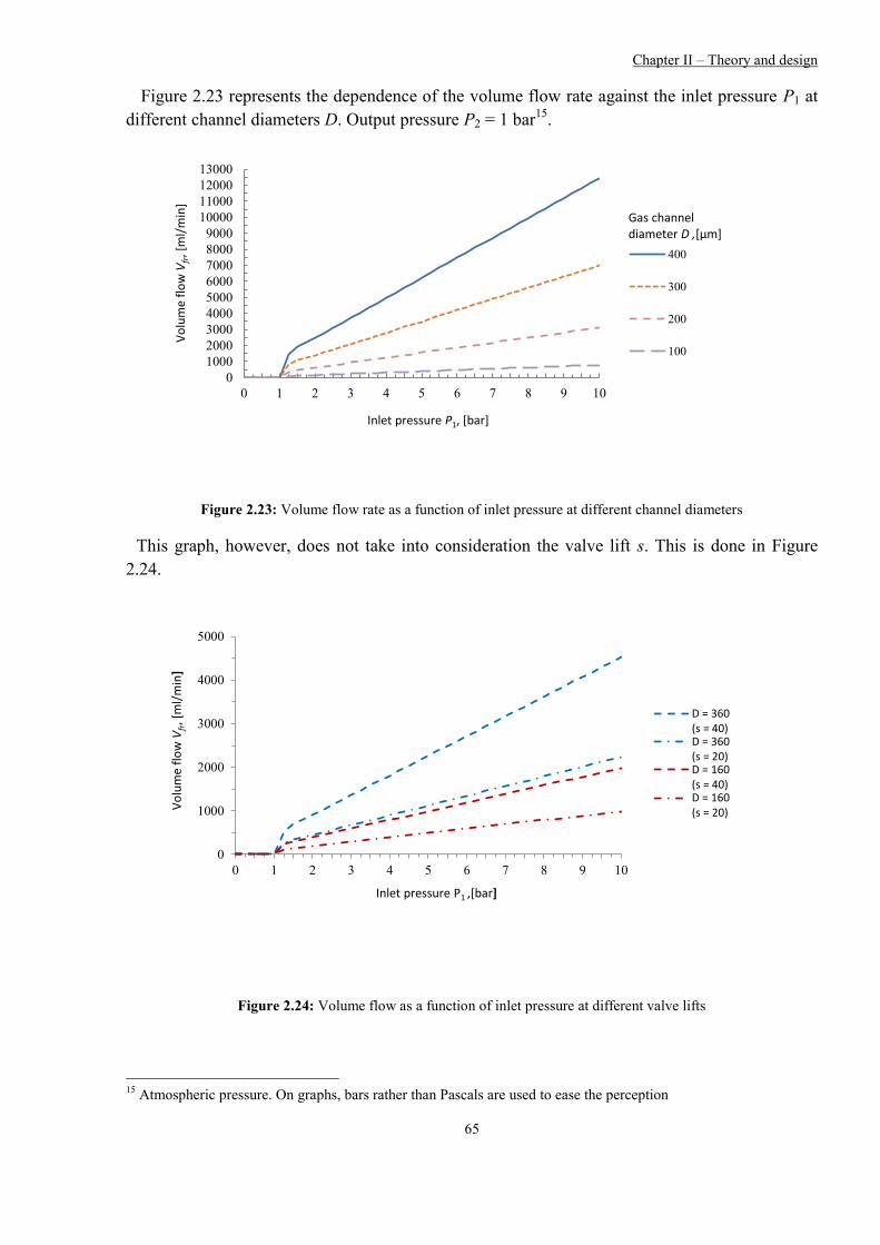
Chapter II – Theory and design
65
Figure 2.23 represents the dependence of the volume flow rate against the inlet pressure P1 at
different channel diameters D. Output pressure P2 = 1 bar15
.
0
1000
2000
3000
4000
5000
6000
7000
8000
9000
10000
11000
12000
13000
0 1 2 3 4 5 6 7 8 9 10
400
300
200
100
Gas channel diameter D ,[µm]
Vo
lum
e fl
ow
Vfr, [
ml/
min
]
Inlet pressure P1, [bar]
Figure 2.23: Volume flow rate as a function of inlet pressure at different channel diameters
This graph, however, does not take into consideration the valve lift s. This is done in Figure
2.24.
0
1000
2000
3000
4000
5000
0 1 2 3 4 5 6 7 8 9 10
Vo
lum
e fl
ow
Vfr, [
ml/
min]
Inlet pressure P1 ,[bar]
D = 360(s = 40)D = 360(s = 20)D = 160(s = 40)D = 160(s = 20)
Figure 2.24: Volume flow as a function of inlet pressure at different valve lifts
15
Atmospheric pressure. On graphs, bars rather than Pascals are used to ease the perception

Chapter II – Theory and design
66
As follows from the graph, larger diameters and valve lifts result in higher volumetric flows at
a given inlet pressure. Additionally, larger diameters require higher values of the valve lifts.
Lager valve lifts in turn, would result in higher pull-in voltages and larger gas channel diameters
would increase the risk of leakage. To avoid the latter, the width of the beam should be
increased, which is an unwanted change in the design. Thus, the valve lift s was chosen to lie in
the range of < 20 µm at the length Lgi (see Fig. 2.22).
2.2.6 Design check
In order to check the design, a simple method was chosen. In the closed state, the actuator of
any design proposed (see Table 2.2) must be able to withstand an inlet gas pressure up to 8-9 bar.
There are three main forces acting on the beam as it is in the pulled-in position:
- Fel – electrostatic force between the beam and bottom electrode.
- Fpn – pneumatic force of gas flow
- Fto – tear-off force due to internal stress gradient
Figure 2.25 schematically illustrates this concept.
Figure 2.25: Forces acting on the actuator’s beam in the pulled-in state
The force Fel keeps the actuator pulled in, while the forces Fto and Fp work against pull-in
state.In order to keep the actuator stably closed, the following condition must be fulfilled
topel FFF (2.75)
In a closed state, the actuator and bottom electrode can be treated as a parallel plate capacitor.
Therefore, Fel can be calculated using Equation 2.12.
Pneumatic force of a gas pressure Fp can be calculated as
inp APPF )( 21, (2.76)
where

Chapter II – Theory and design
67
P1 – inlet gas pressure (here P1 = 9 bar)
P2 – outlet gas pressure (here P2 = 1 bar)
Ain – cross-sectional area of a gas inlet channel
Gas inlet channel is a cylinder with circular cross-section of a diameter D. Thus,
4
2DAin (2.77)
The tear-off force Fto is defined as [51]
t
b
Rtto s
L
cksF
33 (2.78)
Now, it is possible to estimate the influence of all the forces and to check if the actuator beam
will stay closed at given geometries and conditions. The geometrical parameters were taken
from Table 2.2. The diameter D was chosen to lie between 100 and 300 µm. The pull-in voltage
Upi = 12 V.
0
20
40
60
80
100
120
1.1 1.2 1.3 2.1 2.2 2.3 3.1 3.2 3.3 4.1 4.2 4.3 5.1 5.2 5.3
Forc
e, [
mN
]
Design ID
Fel
Fp+Fto, D=100 µm
Fp+Fto, D=200 µm
Fp+Fto, D=300 µm
Figure 2.26: Comparison of forces acting on the actuator's beam in a pulled-in state (Upi = 12 V)

Chapter II – Theory and design
68
Figure 2.26 shows that though as previously determined larger diameters return higher flows,
they also lead to instability of the actuators state. Therefore, for the first production and
characterization a minimal diameter of 100 µm was chosen.
2.3 Microactuator design summary
In the subsections 2.1 and 2.2, the main design parameters of the actuator and microvalve were
considered and estimated. Fifteen design variants of the actuator were proposed. Table 2.4
summarizes the calculated values and the design variants to give an overview of the expected
system performance.
Table 2.4: Summary of the calculated parameters for different actuator design variants
Design ID
St. defl. st
at Lb,
[µm]
Valve lift
s at Lgi,
[µm]
Pull-in
voltage
Upi, [V]
Min.
stand-off
height hb,
[nm]
Reaction
time tr,
[ms]
Inlet
diameter
D, [µm]
Flow rate
Vfr,
[ml/min]
1.1 13 6 8,4 200 1,6 100 31
1.2 13 6 8,4 200 1,6 100 31
1.3 13 6 8,4 200 1,6 100 31
2.1 19 9 9,3 200 2,4 100 46
2.2 19 9 9,3 200 2,4 100 46
2.3 19 9 9,3 200 2,4 100 46
3.1 26 12 9,8 200 3,0 100 62
3.2 26 12 9,8 200 3,0 100 62
3.3 26 12 9,8 200 3,0 100 62
4.1 35 15 10,4 200 4,3 100 77
4.2 35 15 10,4 200 4,3 100 77
4.3 35 15 10,4 200 4,3 100 77
5.1 44 19 11,1 200 5,1 100 98
5.2 44 19 11,1 200 5,1 100 98
5.3 44 19 11,1 200 5,1 100 98
For a production of the systems designed in this chapter, a set of photolithography masks was
created. The drawings of the masks can be found in Appendix I.

Chapter III – Technology and fabrication
69
3 Technology and fabrication
In this chapter, the aspects of technology and fabrication of the microactuator and its
integration into simple prototype microvalve will be discussed. The chapter begins with an
introduction subsection, in which the basic direction of the work on the technology as well as the
main achieved results will be discussed. The following subsections will be dedicated to the
detailed review of each of the topic.
3.1 Introduction
The following subsections will describe in detail experimental activities aimed on the
development of the technological process for the production of the microactuator designed in the
Chapter 2.
The entire process of the development of the technological process done in this work can be
subdivided in several main phases. They include
I. investigation of the actuators producibility by means of electroplating
II. choice of substrate material
III. fabrication of a passive actuator (no bottom electrode)
IV. fabrication of an active actuator (with bottom electrode and contacts)
V. process development for integration of the actuator into a microvalve.
During phase I, it was necessary to define the critical parameters of the galvanic process of Ni
deposition in order to find out, which of these parameters have the most significant influence on
the internal stress gradient. Although it was earlier determined, that the most critical parameter
would be current density [51], a set of new measurements was conducted, since the process
appeared to be very sensitive to the variation of such factors as electrolyte pH value and
temperature. Agitation of the electrolyte showed influence on the uniformity of the metal
deposition over the wafer surface.
Phase II was dedicated to the choice of the substrate material. At first sight, it is obvious to
simply take a standard Si substrate, as it has proven characteristics and is a standard both in
MEMS R&D and in industry. However, a question of an alternative substrate introduction was
considered. First, two variants were proposed: Al2O3 ceramic substrates and Flame Retardant
Class 4 (FR-4) glass reinforced epoxy laminate being used for example for printed circuit boards
(PCB) production. As it was thought, the use of such substrates could bring process
simplification and consequently cost reduction. Furthermore, investigation of their integribility
into standard production steps, especially electroplating, was of technological interest. Finally,
for the reasons described in the dedicated subsections, it was decided to work with 4-inch Si
substrates.
Phase III included several runs of subsequent surface micromachining steps focused on
electroplating and wet etching of sacrificial layers in order to check the reproducibility of the

Chapter III – Technology and fabrication
70
deposition process and correspondence of the actuators final geometry to the theoretical
expectations.
During Phase IV, bottom electrodes were added in order to make the actuator functional.
In Phase V, a through silicon microchannel was introduced underneath the actuator structure,
turning the chip into a microvalve element where the actuator can serve as an open-close
element.
Microfabrication was performed in the clean-room of the Institute for Microsensors, actuators
and systems (IMSAS) of the University of Bremen. The clean room is of class ISO6 (Class 1000
according to the US FED STD 209E).
3.2 Characterization of Ni electroplating process
Ni electroplating is the central part of the whole actuator fabrication process. Two subsequently
plated layers of Ni form a microactuator beam. The process defines the beams geometry and its
mechanical properties. The main challenge was to find out which process parameters influence
the final characteristics at most.
As it was shown in earlier works dedicated to Ni electroplating and held out at the IMSAS [51],
the most significant role belongs to the following parameters:
- current density
- electrolyte pH value
- electrolyte temperature
The shape of current, or voltage signal proved to be of little importance for the process [51].
The current density influences the internal stress of the layer. Hence, one had to find out the
interrelation between these two parameters. Although this was also already investigated in the
above mentioned works, the importance of the parameter claims that it must be additionally
controlled.
To complete this task, a set of 25 4-inch 525 µm thick Si wafers were taken. Each wafer was
wet oxidized with 500 nm of thermal SiO2. Then, a plating base of 15 nm of chromium and 80
nm of gold was sputtered on the whole top surface of each wafer. After that, the wafers were
ready for the electroplating of two Ni layers.
The set of 20 wafers was separated in two main groups. Group 1 included wafers from 1 to 12.
This group was electroplated with Ni layer of thicknesses from approx. 2,4 µm to 3,0 µm.. Inside
this group, the wafers were additionally subdivided into 4 subgroups of 3 wafers. Each subgroup
was electroplated with different current density. Electrolyte used was a commercially available
standard nickel sulfamate solution with pH of 3.5, which was controlled manually for every
wafer. Process temperature was 52° C. Agitation of the electrolyte was involved. Table 3.1
illustrates the experimental setup.

Chapter III – Technology and fabrication
71
Table 3.1: Ni layer stress measurement order. Wafers 1 to 12
Wafer
ID
Layer
material
Ni layer thickness,
[µm]
Current density,
[mA/cm2]
1 Ni 2,69 6
2 Ni 2,89 6
3 Ni 2,87 6
4 Ni 2,91 11
5 Ni 3,03 11
6 Ni 2,83 11
7 Ni 2,83 17
8 Ni 2,73 17
9 Ni 2,80 17
10 Ni 2,39 25
11 Ni 2,72 25
12 Ni 2,75 25
The second group of wafers (wafers from 13 to 20) were electroplated with Ni layer of
thicknesses from 5,6 µm to 6,1 µm using the same electrolyte under the same pH and
temperature conditions with agitation. As in previous setup, wafers were additionally subdivided
into 4 subgroups of 2 wafers. Again, each subgroup was electroplated with different current
density. The experimental setup is shown in Table 3.2.
Table 3.2: Ni layer stress measurement order. Wafers 13 to 20
Wafer
ID
Layer
material
Ni layer thickness,
[µm]
Current density,
[mA/cm2]
13 Ni 6,08 6
14 Ni 6,10 6
15 Ni 5,80 11
16 Ni 5,78 11
17 Ni 5,72 17
18 Ni 5,64 17
19 Ni 5,47 25
20 Ni 5,55 25
The measurements of the stress were held out with the stress measurement device “Eichhorn &
Hausmann” MX-203 similar to the one shown in Figure 3.1.

Chapter III – Technology and fabrication
72
Figure 3.1: Wafer geometry gauge Eichhorn & Hausmann MX-203 [66]
The device is capable of measuring one wafer per measurement run. The measurement run
takes approximately 5 seconds. The wafer is normally measured at five points: left, right, top,
bottom, and center. The whole measurement process is programmed and controlled by a PC with
dedicated software. The measurement data are stored on the hard disc of the PC.
The graphs in Figure 3.2 and 3.3 show strong dependence of stress on current density for both
thicknesses. Using these data, it was possible to adjust correct plating parameters to achieve the
desired beam bending. The plating of the bottom and top Ni layers was found to be stable under
the following conditions:
Layer 1 (bottom)
Temperature: T = 52 °C
Electrolyte pH: 3,2
Current density: 17 mA/cm2
Stress: ≈ -20 MPa
Layer thickness: d1 ≈ 2 µm
Layer 2 (top)
Temperature: T = 52 °C
Elektrolyte pH: 3,2
Current density: 10 mA/cm2
Stress: ≈ 12 MPa
Layer thickness: d2 ≈ 18 µm

Chapter III – Technology and fabrication
73
Figure 3.2: Ni layer stress vs. current density at layer thickness from 2.4 to 3 µm
Figure 3.3: Ni layer stress vs. current density at layer thickness from 5.5 to 6 µm
These parameters had been later involved in the final technological flow.
3.3 Choice of substrate material
Three substrate materials were initially proposed:
- conventional silicon substrate,
- Al2O3 ceramic (alumina) substrate, and

Chapter III – Technology and fabrication
74
- Flame Retardant Class 4 (FR-4) glass reinforced epoxy laminate substrate.
The two latter ones could have possible technological advance, since on the one hand, they are
capable of being preprocessed. For example, electrical contacts and gas channels could be
produced before actuator electroplating. On the other hand, these materials are isolators. Hence,
no oxidation layers need to be deposited, as in case of silicon.
There was also a clear technological interest, if it was possible to integrate such substrates into
a conventional electroplating, and to carry on other standard MEMS processes on them without
too many changes.
On the other hand, very often, not only surface but also bulk micromachining must be
performed somewhere in the technological flow. Such treatment is not usual for ceramics and
FR-4. This could lead to complications and make the overall process very expensive. Moreover,
unless high production volumes are provided, it is hard to find a supplier of such preprocessed
substrates who could provide them for a reasonable price. In addition to that, a substrate must
have a shape of a conventional 4-inch wafer, which is also not common for FR-4, but turned out
to be possible for ceramics.
For these reasons, FR-4 was excluded from this work and remains open for future
investigations. Alumina was investigated as described in the next subsection. Finally,
conventional silicon substrates were chosen, due to their robustness, technological flexibility and
availability in comparison to the others.
3.3.1 Al2O3 substrate study
3.3.1.1 Alumina: basic information
Aluminum oxide Al2O3 or alumina is the most important, widely used and cost effective oxide
ceramic material. The material possesses strong ionic bonding, which determines its material
properties:
- high mechanical strength (flexural strength) and hardness;
- high wear resistance;
- high resistance to chemical attacks of strong acids and alkali even at high temperatures;
- high stiffness;
- excellent insulating properties;
- low coefficient of thermal expansion;
- good fracture toughness;
- good thermal conductivity;
- good biocompatibility.
Aluminum ceramics parts are manufactured by the following technologies: uniaxial (die)
pressing, isostatic pressing, injection molding, extrusion and slip casting. Aluminum ceramics
are widely used in electronics and electrical engineering, metallurgical processes, chemical
technologies, medical technologies, mechanical engineering, military equipment.

Chapter III – Technology and fabrication
75
Aluminum ceramics are used for manufacturing insulators, capacitors, resistors, furnace tubes,
sealing refractory parts, foundry shapes, wear pads, thermocouple protection tubes, cutting tools
and polishing/grinding powders, ballistic armor, laboratory equipment, bio-ceramic parts for
orthopedic and dental surgery, bearings and of course substrates.
The technical alumina ceramics contain at least 80% of aluminum oxide (KER 706). There are
also alumina types KER 708 (90% - 99% of Al2O3), and KER 710 (>99% of Al2O3). The rest of
the material is usually SiO2. In this work, 4-inch wafer shaped alumina substrates with purities of
91%, 96% and 99,6% were processed.
Wet and dry processing of alumina is possible. Dry etching can only be performed using very
special and expensive techniques, such as [67]
- Laser etching with CF4
Gas: CF4
Energy source: XeCl-Laser, λ = 308 nm
- RIE in a mixture of Cl2 and Ar
Gas mixture: 71 Vol. % Ar; 29 Vol. % Cl2
Plasma conditions: 0.933 Pa, -750 V bias
Energy source: XeCl-Laser, λ = 308 nm
- RIE in CH2F2 or CH3F
Gas: either 100% CH2F2 or CH3F
Plasma condition: 0.027 Pa
Ion energy: 0.8 kV
Ion flow density: 0.6 mA/cm2 (angle of incidence 30°)
At the time of this project, these processes were not available at the IMSAS on the one hand,
due to the lack of equipment. On the other hand, due to the fact that some important parts of the
RIE tool are also made of ceramic materials and could be damaged during high power
processing. Processing with lower power would not return reasonable etching rates.
Hence, the main focus was concentrated on the wet etching of the alumina. As it has been
already stated above, the material has high resistance to such a processing. Therefore there is no
much information on how to do it. Only several literature sources were found [68]. In these
sources, however, very special techniques and tools were used to achieve the results.
Nevertheless, it is known that alumina can be etched by phosphoric acid (H3PO4) and nitric acid
(HNO3) [68]. It is also known that the resistivity to chemical reaction is directly proportional to
the purity and inversely proportional to the porosity of the alumina. The goal of this project part
was to find out if it would be possible to etch the alumina using simpler wet etching approaches.
3.3.1.2 Wet etching experiments
Table 3.3 sums up the experimental setups used in this work to determine the etchibility of the
alumina substrates in wet etchants.

Chapter III – Technology and fabrication
76
Table 3.3: Wet etching experimental setups
Take
No.
Substrate Etchant
Time,
h
Mask,
Yes/No
Mask
material Result
Supplier Type Purity,
%
Surface
roughness
Ra, [µm]
Type Temp.,
°C
1.1 CeramTec Rubalit
708S 96 0.1 PWS 35 3.5 No - +
1.2 CeramTec Rubalit
708S 96 0.1
H3PO4
(85%) 55 3.5 No - +
2.1 N.D. KER710 99.6 1 PWS 35 4 Yes Cr -
2.2 N.D. KER710 99.6 1 H3PO4
(85%) 55 4 Yes Cr -
3.1 CeramTec Rubalit 710 99.6 0.1 PWS 35 4 Yes Cr -
3.2 CeramTec Rubalit 710 99.6 0.1 H3PO4
(85%) 55 4 Yes Cr -
4.1 CeramTec Rubalit 710 99.6 0.1 PWS 65 6 Yes Cr -
4.2 CeramTec Rubalit 710 99.6 0.1 H3PO4
(85%) 85 6 Yes Cr -
5.1 CoorsTek KER708 91 >1 PWS 35 5 Yes Photoresist
TI35 -
5.2 CoorsTek KER708 91 >1 H3PO4
(85%) 55 5 Yes
Photoresist
TI35 -
An 85%-solution of phosphoric acid (H3PO4) and the PWS-solution16
were used. The table
also shows the result of the experiment. A “+”-sign in the right most column means that etching
was observed. In the following, more detailed description of the experiments will be given.
Take 1
The first two substrates were rectangular pieces of ceramic type 708 with purity of 96%. Before
etching, it was cleaned in peroxymonosulfuric acid17
. Due to nonstandard shape of the substrate,
no mask was used in this take. Hence, in order to find out if any etching took place or not, a set
of 7 preliminary contact thickness measurements was done. After the etching, the thickness was
measured again on the same positions. This is illustrated in Figure 3.4. Process parameters can
be found in Table 1.3.
16
PWS (Ger.: Phosphorsäure – Wasser - Salpetersäure) – a mixture of 80% of H3PO4, 16% of H2O, and 4% of
HNO3.
17 Also known as Caro’s acid.

Chapter III – Technology and fabrication
77
Figure 3.4: Contact thickness measurement points on the substrate.
For each point, five contact thickness measurements in a row were taken. The measurement
results for both PWS and H3PO4 etching tests are represented on the graphs in Figures 3.5 and
3.6 respectively. In these graphs, the mean values and standard deviations σ are represented.
Figure 3.5: Graphical representation of the etching results in PWS.
Figure 3.6: Graphical representation of the etching results in H3PO4.

Chapter III – Technology and fabrication
78
Both graphs show that etching of the alumina of the type 708 is possible both with PWS and
85% solution of H3PO4. The etch rates were determined to be around 40 nm/min in H3PO4, and
around 50 nm/min in PWS. PWS seems to etch a little faster on the first sight. Thought, taking
into consideration the standard deviation of about 30% it is hard to say, which of two is really
faster. It was also noted, that in both cases, etching in the center of the substrates (point 4) is
much slower than on the edges. Possible explanation could be that the contact surface between
the substrate and the chemical is larger on the edges, i.e. solution can attack not only from the
top or the bottom, but also aside. Furthermore, some admixtures or contamination could occur in
this area. Although, this is unlikely that contamination occurred exactly on the same position of
several substrates.
After relatively successful etching without masking, further takes with patterned chromium or
photoresist layers as masks were planned and executed.
Take 2
The second set of substrates of type KER710 with higher purity of 99.6% but lower surface
roughness of Ra = 1 µm was also etched in PWS and 85% solution of H3PO4. Taking into
consideration higher purity of the material, etching time was increased up to 4 hours for both
solutions. The substrates had the shape of a 4 inch18
square wafer. Thus, it was possible to
process them, though with some restriction, with common tooling.
First, both substrates were cleaned in peroxymonosulfuric acid. A 50 nm thick chromium layer
was then sputtered on the top side of the substrate. After that, a spin coating of a 2 µm thick
positive photoresist and common exposure and development steps were done19
. Two masks with
different test structures were used for this and all the following takes. Then, chromium was wet
etched in the commercially available “Chrom Etch 3144” solution by Honeywell. The remaining
photoresist was stripped away with acetone and isopropanol. The back side of the substrates was
then completely sputtered with 100 nm thick layer of chromium in order to avoid alumina
etching elsewhere except of the opened areas on the front side.
Figure 3.7 shows two alumina substrates covered with patterned chromium layer.
18
Side length
19 Since it was only a single layer process, no precision mask alignment was needed. Later on, when a multilayer
process was introduced, alignment problems due to surface roughness and scattering came into play. This issue will
be described in a dedicated section below.

Chapter III – Technology and fabrication
79
Figure 3.7: KER710 Substrates covered with patterned chromium layer:
mask variant 1 (left), mask variant 2 (right)
A step measurement on the contact profilometer Alpha-Step was done. But it did not show
return any step between alumina surface and chromium surface due to very high surface
roughness of alumina. It was expected, that after wet etching the step will be seen.
Finally, wet etching of the substrate 1 in PWS and substrate 2 in H3PO4 was performed and
contact measurement of both substrates was done again. Unfortunately, as before, no difference
was detected. Either no etching at all took place, or the sensitivity of the profilometer is too low
to detect it compared to surface roughness.
It was expected that alumina with higher purity would possess higher durability against wet
etching. Still, it was expected to find at least slight material removal. Therefore, it was decided to
use the substrates of the same purity, but with finer surface.
Take 3
In this take, all the processes and parameters of the previous take were used. The only
difference was in the substrates. This time, the substrates with surface roughness of Ra = 0.1 µm
were taken. These substrates of type 710 provided by the company CeramTec had the shape of a
common 4 inch silicon wafer. Thus, it was possible to process them with common tools without
significant issues. Before wet etching, both substrates were broken into 4 parts in order to be able
to process 1 wafer at least 4 times with different conditions, if needed (Fig. 3.8) Parts 1 and 2
were utilized in take 3, whereas parts 3 and 4 were postponed for take 4.

Chapter III – Technology and fabrication
80
Figure 3.8: Broken CeramTec Rubalit 710 substrate covered with chromium mask
Unfortunately, after 4 hours of wet etching neither substrate 1, which was etched in PWS, nor
substrate 2, which was etched in H3PO4, showed traces of the material removal.
Take 4
In this take, the same material as in previous take was utilized. The etching parameters were
changed. First of all, temperature of both etchants was raised to 65°C for PWS and 85°C for
H3PO4. Etching time was increased up to 6 hours for both runs.
After the runs, the step height was again measured with alpha-step contact profilometer. As
before, no material removal was observed.
Take 5
In the final take, a material with lower purity was utilized. It was two alumina substrates of
type 708with purity of 91% supplied by the company CoorsTek. This time, instead of chromium,
a 3 µm thick positive photoresist TI35 was used as the mask for wet etching in order to reduce
the costs of the experiment. This photoresist possesses a very high resistivity against wet etching
solutions and high temperatures. Before coating with resist, an adhesion promoter was deposited
on the surface of the substrates. The resist was then exposed and developed using standard
procedures. Figure 3.9 shows the substrate covered with patterned resist mask.

Chapter III – Technology and fabrication
81
Figure 3.9: Alumina KER 708 91% covered with TI35 photoresist mask
The etching was performed in PWS and in 85% solution of H3PO4.
As in previous takes, contact measurements of the step height on different positions using
alpha-step tool were performed both before and after the etching. No material removal was
observed.
3.3.1.3 Electroplating of Ni onto an Al2O3 substrate
The point of the following experiment was to investigate a principal possibility to produce
nickel actuator on a ceramic substrate by means of electroplating. This could ensure the
utilization of such wafers in the processes where no bulk micromachining would be foreseen. In
order to do it, an already existing at the moment electroplating process, described in literature
before [51] was used. Since it was developed at the IMSAS, all the masks could also be directly
used.
Five 4-inch 500 µm thick polished down to Ra = 0.1 µm alumina wafers of type Rubalit KER
710 supplied by CeramTec were taken for the experiment.
The production process began with conventional cleaning in the peroxymonosulfuric acid.
Since alumina is an insulator, no substrate thermal oxidation was needed. After cleaning, a seed
layer of 15 nm of Cr and 80 nm of Au was sputtered over the surface of the substrate followed
by sputtering of 500 nm of Cu. Then, the first lithography step defining the opening in Cu for an
anchor of the actuator was performed. First, wafers were heated on a hot plate at 120°C for 2
min. in order to remove possible moisture. Then, adhesive agent TI-Prime was spin-coated.
Thereupon, the wafers were heated on a hot plate at 100°C for 2 min. After that, a positive 1,8
µm thick photoresist AZ®1518 was semiautomatically spin-coated over the surface of the wafer,
followed by a softbake step on a hot-plate at 120°C for 2 min. The contact vacuum 2.2 sec. long
exposure with UV-light was performed on a Süss MA6 mask aligner. At this point, no precision
alignment was needed. After the development step, the resist was additionally hardbaked on a
hot-plate for 2 min. at 100°C. After that, a descumming in oxygen plasma was done. This step
ensures that no photoresist residuals are left in the developed zones. Cu was then wet etched in
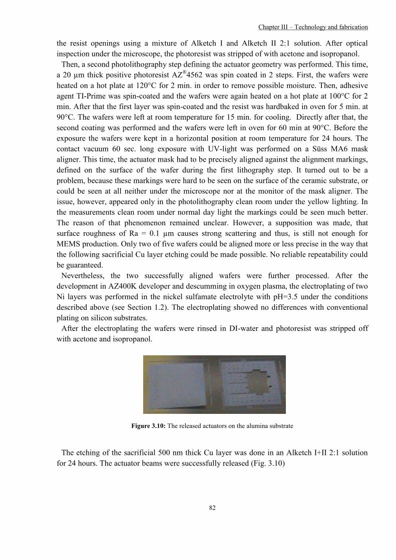
Chapter III – Technology and fabrication
82
the resist openings using a mixture of Alketch I and Alketch II 2:1 solution. After optical
inspection under the microscope, the photoresist was stripped of with acetone and isopropanol.
Then, a second photolithography step defining the actuator geometry was performed. This time,
a 20 µm thick positive photoresist AZ®4562 was spin coated in 2 steps. First, the wafers were
heated on a hot plate at 120°C for 2 min. in order to remove possible moisture. Then, adhesive
agent TI-Prime was spin-coated and the wafers were again heated on a hot plate at 100°C for 2
min. After that the first layer was spin-coated and the resist was hardbaked in oven for 5 min. at
90°C. The wafers were left at room temperature for 15 min. for cooling. Directly after that, the
second coating was performed and the wafers were left in oven for 60 min at 90°C. Before the
exposure the wafers were kept in a horizontal position at room temperature for 24 hours. The
contact vacuum 60 sec. long exposure with UV-light was performed on a Süss MA6 mask
aligner. This time, the actuator mask had to be precisely aligned against the alignment markings,
defined on the surface of the wafer during the first lithography step. It turned out to be a
problem, because these markings were hard to be seen on the surface of the ceramic substrate, or
could be seen at all neither under the microscope nor at the monitor of the mask aligner. The
issue, however, appeared only in the photolithography clean room under the yellow lighting. In
the measurements clean room under normal day light the markings could be seen much better.
The reason of that phenomenon remained unclear. However, a supposition was made, that
surface roughness of Ra = 0.1 µm causes strong scattering and thus, is still not enough for
MEMS production. Only two of five wafers could be aligned more or less precise in the way that
the following sacrificial Cu layer etching could be made possible. No reliable repeatability could
be guaranteed.
Nevertheless, the two successfully aligned wafers were further processed. After the
development in AZ400K developer and descumming in oxygen plasma, the electroplating of two
Ni layers was performed in the nickel sulfamate electrolyte with pH=3.5 under the conditions
described above (see Section 1.2). The electroplating showed no differences with conventional
plating on silicon substrates.
After the electroplating the wafers were rinsed in DI-water and photoresist was stripped off
with acetone and isopropanol.
Figure 3.10: The released actuators on the alumina substrate
The etching of the sacrificial 500 nm thick Cu layer was done in an Alketch I+II 2:1 solution
for 24 hours. The actuator beams were successfully released (Fig. 3.10)

Chapter III – Technology and fabrication
83
3.3.2 Substrate choice: conclusion
Two alternatives to a conventional silicon substrate were chosen:
- Al2O3 ceramic (alumina) substrate, and
- Flame Retardant Class 4 (FR-4) glass reinforced epoxy laminate substrate.
The latter one was excluded from the experimental work due to difficulties with its small
volume commercial availability in a 4 inch wafer shape.
Different types of Al2O3 were investigated. First, wet etching experiments were performed in
an attempt to find out a simple and cost effective ceramic wet etching method as well as the most
suitable ceramic type. In spite of some successful runs with the substrates of type 708 in the first
take, the overall result is negative and no etching of the alumina ceramic using simple wet
chemical approaches is possible and can be recommended for current work and further
production. Separate research can be done in order to find out as to why only one of three types
of the ceramic substrates could be processed. One possible explanation could be that ceramics of
type 708 with 96% of Al2O3 has 4% of soluble silicate binding agents, whereas type 710 has
only 0.4% of them. Thus, type 708 is more suitable for wet etching [69]. It is of course of
interest, what chemical reactions run in this case. This does not, however, explain why 91%
ceramic could not be etched, either, although it has even greater part of silicate binding agents. In
future work, other ceramic types must be investigated.
Nevertheless, the utilization of such wafers in the processes where no bulk micromachining
would be foreseen had to be checked as well. In order to do this, a set of five 4-inch 500 µm
thick polished down to Ra = 0.1 µm alumina wafers of type Rubalit KER 710 supplied by
CeramTec was taken. Using the technology of the passive actuator from previous works [51], it
was proven, that most of ceramic substrates of this type are in principal suitable for most of the
conventional silicon technology steps involved.
The only serious issue found was impossibility of precise and repeatable alignment of the
photoresist coated substrate during the second lithography step due to almost invisible alignment
markings. This issue makes the whole process unreliable. The reason of it remained unclear.
Although the assumption was made that the roughness of the substrate surface must be much
better than Ra = 0.1 µm. This, however, would make the substrates more expensive.
Based on the experimental material collected above, it can be concluded, that for the R&D
work conventional silicon substrates remain the most effective solution.
3.4 Actuator fabrication
In this subsection, the production related questions are discussed in detail. Precise descriptions
of technological flows for production of passive and active (with electrical contacts) actuators as
well as for a microvalve are given.

Chapter III – Technology and fabrication
84
3.4.1 Fabrication of photomasks
The process of the actuator/valve fabrication incorporated from 2 to 5 photolithography steps
depending on the complexity of the device20
. In order to reduce the costs, it was decided not to
purchase the expensive chromium-glass masks, but to produce them at the IMSAS using
preordered foil masks. The dimensions of the structure as well as not very strict resolution
requirements allowed doing so.
For that purpose, 4 inch borosilicate glass wafers were utilized. After conventional cleaning in
the peroxymonosulfuric acid, the wafers were sputtered with 100 nm of Cr. Then, a
photolithography with 2 µm thick positive photoresist and a corresponding foil mask was done
similar to the first photolithography step described in Subsection 1.3.1.3. The foil masks were
glued to the glass in order to make the placement into the mask aligner and the exposure
possible. Cr was then etched with “Chrom Etch 3144” etcher, and the resist was stripped off with
acetone and isopropanol. Figure 3.11 shows an example of one of the produced masks.
Figure 3.11: First design of a borosilicate glass photomask for bottom electrodes
3.4.2 Fabrication of a passive actuator
In this subsection, the fabrication of a passive actuator will be described. Passive actuator has
neither bottom electrode nor contacts. No isolation layer was deposited, neither. The structure
only incorporates seed layer, insulation layer and an actuator beam. This makes the fabrication
much simpler. However, the flow includes many core processes, such as electroplating, PVD,
lithography, wet and dry etching. The aim of the experiments was to tune these core processes
before a step to more advanced processes could be made.
First, a step-by-step description of the process flow will be given. Then, the issues met during
the work will be discussed, following by a short conclusion.
20
From simple passive actuator to a complex integrated microvalve

Chapter III – Technology and fabrication
85
3.4.2.1 Process flow description
Figure 3.12 gives a schematic representation of the process flow of the passive actuator
production.
1.
5.
2.
6.
3.
7.
4.
8.
Figure 3.12: Passive microactuator production flow
A production lot with five 4 inch 380 µm thick silicon wafers was used for the production. The
process began with conventional cleaning in the peroxymonosulfuric acid. Thereupon, a wet
thermal oxidation was done. SiO2 of 500 nm thickness was grown on both sides of the wafer
(Fig. 3.12.1). Next, a seed layer of 15 nm of Cr and 80 nm of Au was sputtered over the surface
of the substrate followed by sputtering of additional 15 nm of Cr (Fig. 3.12.2). The latter would
be used as a material for bottom electrodes in the next technology research phase. Here, it was
sputtered in order to study its reliability and interaction with other basic processes. It was not
structured. Hence, no real electrodes were present.
The next step was a subsequent sputtering of 100 nm of Ti and 300 nm of Cu as a sacrificial
layer for the future actuator release etching (Fig. 3.12.3). Then, the first and second lithography
steps defining the antistiction bumps and actuator attaching area were performed (Fig 3.12.4).
First, wafers were heated on a hot plate at 120°C for 2 min. in order to remove remaining
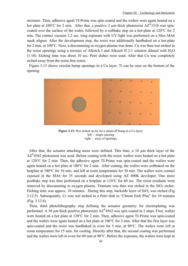
Chapter III – Technology and fabrication
86
moisture. Then, adhesive agent TI-Prime was spin-coated and the wafers were again heated on a
hot plate at 100°C for 2 min. After that, a positive 2 µm thick photoresist AZ®1518 was spin-
coated over the surface of the wafer, followed by a softbake step on a hot-plate at 120°C for 2
min. The contact vacuum 2.2 sec. long exposure with UV-light was performed on a Süss MA6
mask aligner. After the development step, the resist was additionally hardbaked on a hot-plate
for 2 min. at 100°C. Next, a descumming in oxygen plasma was done. Cu was then wet etched in
the resist openings using a mixture of Alketch I and Alketch II 2:1 solution diluted with H2O
(1:10). Etching time was about 10 sec. Petri dishes were used. After that Cu was completely
etched away from the resist-free zones.
Figure 3.13 shows circular bump openings in a Cu layer. Ti can be seen on the bottom of the
opening.
Figure 3.13: Wet etched cavity for a stand-off bump in a Cu layer:
left – single opening
right – array of openings
After that, the actuator attaching areas were defined. This time, a 10 µm thick layer of the
AZ®4562 photoresist was used. Before coating with the resist, wafers were heated on a hot plate
at 120°C for 2 min. Then, the adhesive agent TI-Prime was spin-coated and the wafers were
again heated on a hot plate at 100°C for 2 min. After coating, the wafers were softbaked on the
hotplate at 100°C for 10 min. and left at room temperature for 30 min. The wafers were contact
exposed in the MA6 for 35 seconds and developed using AZ 400K developer. One more
postbake step was then performed on a hotplate at 110°C for 60 sec. The resist residuals were
removed by descumming in oxygen plasma. Titanium was then wet etched in the SiO2 etcher.
Etching time was approx. 10 minutes. During this step, backside layer of SiO2 was etched (Fig
3.12.5). Subsequently, Cr was wet etched in a Petri dish in “Chrom Etch Plus” for 10 minutes
(Fig. 3.12.6).
Then, third photolithography step defining the actuator geometry for electroplating was
performed. A 30 µm thick positive photoresist AZ®4562 was spin coated in 2 steps. First, wafers
were heated on a hot plate at 120°C for 2 min. Then, adhesive agent TI-Prime was spin-coated
and the wafers were again heated on a hot plate at 100°C for 2 min. After that the first layer was
spin-coated and the resist was hardbaked in oven for 5 min. at 90°C. The wafers were left at
room temperature for 15 min. for cooling. Directly after that, the second coating was performed
and the wafers were left in oven for 60 min at 90°C. Before the exposure, the wafers were kept in

Chapter III – Technology and fabrication
87
a horizontal position at room temperature for 24 hours. The contact vacuum 60 sec. long
exposure with UV-light was performed in a Süss MA6 mask aligner.
After the development in AZ400K developer and descumming in oxygen plasma, the
electroplating of two Ni layers was performed in the nickel sulfamate electrolyte with pH 3.5
under the conditions descried in Section 1.2. Thereupon, the wafers were rinsed in DI-water and
photoresist was stripped off with acetone and isopropanol (Fig. 3.12.7). The sacrificial Ti/Cu
layer was wet etched (Fig. 3.12.8). Cu was etched in Alketch I+II solution in a Petri dish for 24
hours. Ti was etched in SC121
for 30 – 60 min22
in a beaker on a hot-plate. The solution was
constantly agitated. Wafers were fixed inside the beaker with polymer single wafer holder. The
wafers were then washed in DI-water in a quick dump rinser and dried in a spin rinse dryer.
3.4.3 Fabrication of an active actuator
In the following, the fabrication process of an active device variant will be described. This
process basically had three additional steps in comparison with the one discussed in the previous
subsection:
- definition of the bottom electrodes and electric contacts
- deposition of the isolation layer
- formation of the contact openings in the isolation layer
Definition of the bottom electrode included
- deposition of the electrode and contacts layer
- photolithography of the electrodes and contacts layout
- etching of the electrodes
Si3N4 was chosen as an isolation layer. It was deposited over the electrodes using PECVD
technique.
The contact openings in the Si3N4 layer were made by wet etching in the Oxide Etch solution.
3.4.3.1 Process flow description
Since all the steps except those for electrodes, contacts and isolation layer formation are the
same as before, it makes no sense to repeat them again. Detailed description of only the newly
developed ones will be given.
Bottom electrodes
The process of the electrodes and contacts formation begins with sputtering of a sandwich of
Cr/Au/Cr layer with thicknesses of 15 nm / 80 nm / 15 nm respectively over the oxidized surface
21
1:1:5 solution of NH4OH + H2O2 + H2O at 80 °C
22 Time depends on the size of the actuator.

Chapter III – Technology and fabrication
88
of a 4 inch 380 µm silicon wafer. Then, a lithography step with 30 µm thick positive resist
AZ®4562 was performed. Before the exposure, the wafers were hardbaked in oven under 90°C
for 60 min. and afterwards left for 24 hours under room temperature. One more hotplate
postbake step at 110°C for 60 sec. was done after the development.
It had to be decided about the method for etching the Cr layer. Two possibilities existed:
- Wet etching with solutions available at hand: “Crom Etch Plus” from Candor Chemie and
“Crom Etch 3144” from Honeywell
- Dry plasma etching in STS-Tool
First, wet etching with a commercially available “Crom Etch 3144” solution from Honeywell
Intl. was performed. Average etching rate was measured to be approx. 65 nm/min. Thus, only a
short 10 sec. dip was needed to etch away a 15 nm thick layer of Cr.
Optical inspection after the etching showed disproportionally deep (3 to 4 µm) underetching of
Cr (Fig. 3.14).
Cr
Au
Electrode edge
~3 µm
Figure 3.14: Chrome underetching in Chrom-Etch 3144 after 10 sec. dip
Some thin structures were severely damaged or even stripped away (Fig. 3.15).
Cr
Au
Electrode edge
Figure 3.15: Chrome underetching in "Chrom-Etch 3144": thin structure destroyed

Chapter III – Technology and fabrication
89
First suggestion was bad resist adhesion. Thus, a rework was done. All the metallic layers were
etched away, wafers were cleaned and then metallic layers were redeposited. After that, a
lithography sequence of 30 µm thick positive resist AZ®4562 was performed with preliminary Ti
Prime adhesive agent was performed. After that, a lithography sequence of 30 µm thick positive
resist AZ®4562 was performed with preliminary Ti Prime adhesive agent was performed. Post-
development bake step was done with 120°C for 60 sec. Chrome was then 10 sec. dip etched in
“Chrom Etch 3144”. The result was the same: wide underetching profiles.
After several discussions [70], the conclusion was made that the reason for such a phenomenon
is the so called electrochemical corrosion of chrome due to a big difference between the
electrochemical potentials of chrome (-0.74) and gold (+1.52) being together in the acidic
environment of a “Chrom-Etch 3144” solution.
Another chrome etching solution was used: “Chrom Etch Plus”. In spite of all preliminary
procedures to avoid attacking of photoresist by this solution, the resist was severely damaged by
“Chrome Etch Plus”.
Thus, dry etching of chrome in argon plasma in an STS machine was then investigated. The
wafers were sputtered with Cr/AuCr layers and covered with 1.8 µm, 6.5 µm and 10 µm thick
photoresist. Several etching experiments were conducted. First, five wafers with thinnest 1.8 µm
thick photoresist were processed with following parameters:
Power: 20 Watt
Ar-flow: 20 sccm.
Pressure: 8 mTorr
Time: 30 min.
Result: no etching was seen.
The second set of parameters was:
Power: 50 Watt
Ar-flow: 20 sccm.
Pressure: 8 mTorr
Time: 15 min. + 15 min. without pause
Result: chrome was only partly etched. Resist was almost etched away.
For the next try, five wafers with 6 µm thick photoresist were taken. The etching parameters
were
Power: 50 Watt
Ar-flow: 20 sccm.
Pressure: 8 mTorr
Time: 15 min.

Chapter III – Technology and fabrication
90
Result: resist was partly damaged, but not etched away. After the resist strip-off, the etched
profile of the upper chrome layer was measured with the Alpha-Step contact profilometer. The
etching rate was determined to be approximately 2 - 3 nm/min.
Next, five wafers with 30 µm thick resist were processed. This time, it was tried to remove the
Cr/Au/Cr sandwich completely
Power: 50 Watt
Ar-flow: 20 sccm.
Pressure: 8 mTorr
Time: 60 min. without pauses +15 min. +15 min. for the lower Cr layer
Postprocessing: short dip into “Chrome Etch Plus”
Result: Bubbling of the resist, damage of the electrodes geometry.
The next experimental set used five wafers with 10 µm thick photoresist and the following
parameters:
Power: 50 Watt
Ar-flow: 20 sccm.
Pressure: 8 mTorr
Time: 8×15 min. with pause after each 15 min.
Postprocessing: short dip into “Chrome Etch Plus”
The function of pauses is to let the wafer cool down in order to avoid the damage or burning of
the resist.
Result: Cr/Au/Cr sandwich is almost completely etched away; resist ashes on the surface (Fig.
3.16), which could not be cleaned chemically but only manually with the towel dipped in
acetone.
Figure 3.16: Resist ashes on the Cr electrodes surface after Ar-plasma etching

Chapter III – Technology and fabrication
91
It was then obvious that overheating of wafers during the processing is responsible for bad
results. Increase of pause time did not help. Therefore, a special thermal paste was applied on the
back side of the wafer in order to prevent the overheating during the processing. This paste was
then stripped from the wafer and the vacuum chamber of the STS machine manually with the
acetone and towel. The etching was done with the following parameters:
Power: 50 Watt
Ar-flow: 20 sccm.
Pressure: 8 mTorr
Time: 8×15 min.
Postprocessing: short dip into “Chrome Etch Plus”
The etching result is shown on Figure 3.17.
Figure 3.17: Dry etched Cr/Au/Cr electrodes: etching with thermal paste
One more experimental setup was used in order to check, if one more solution could be used.
Five wafers with Cr/Au/Ti (15nm/80nm/50nm) layer electrodes were etched. The upper Ti layer
was first wet etched in a 7:1 Oxide Etch solution for 45 – 60 sec. The rest was etched in argon
plasma for 75 min with thermal paste and pauses each 15 min. Power was 50 Watt, Ar-flow was
20 sccm. und 8 mTorr pressure. Etching was successful. The result is represented on Figure 3.18.
Figure 3.18: Etching result of a Cr/Au/Ti electrode.
Ti layer was wet etced, Cr/Au were dry etched in Ar-plasma

Chapter III – Technology and fabrication
92
It was decided to proceed with the Cr/Au/Cr stack, since later on titanium sacrificial layer
would be etched. Hence, using titanium as a part of the electrode could be risky.
Isolation layer
After successful etching of bottom electrodes, the wafers had to be deposited with an isolation
layer that had to protect the electrodes against short circuiting during the operation. Many
dielectric materials can serve as isolation layers: Si3N4, SiO2, Al2O3 to name a few. Alumina was
excluded due to technologically difficult etching processes, which were described in Chapter 1.3
of this work. SiO2 could be an attractive solution, but the technological process of the system
production included several oxide etch steps where this layer could be directly attacked and
therefore, made SiO2 impossible for use.
PECVD Si3N4 was finally chosen as an isolation layer due to its good dielectric properties and
technological availability. The disruptive strength of Si3N4 is ED,Nitride ≈ 5×10⁶ V/cm [71], which
makes a 100 nm thick layer capable to withstand the voltages up to 100V. In order to guarantee
reliable function of the isolation layer, it was suggested to keep its thickness between 200 nm
and 400 nm. Low-stress Si3N4 layer was deposited. The deposition parameters were:
Deposition time: 18 min.
N2 flow: 1960 sccm
NH3 flow: 50 sccm
SiH4 flow: 40 sccm
Power lf/hf: 31/27 W
Pressure: 902 mTorr
After deposition, the thickness of Si3N4 layer was measured. It ranged from 293.6 to 304.6 nm.
Contact openings
The function of the contact openings is to provide electrical contacts between the voltage
source and the electrodes. The openings must be etched in the Si3N4 isolation layer that covers
the top surface of the wafer completely. Before that, a sacrificial layer of 100 nm of Ti and 300
nm of Cu was sputtered above the layer of Si3N4. Hence, these two materials also had to be
etched. Simultaneous etching of three materials saved at least one lithography step. But on the
other hand, a set of etchants had to be carefully chosen in such a manner that each etching step
would only attack right materials. After a convenient lithography step with 10 µm thick positive
photoresist AZ®4562, the etching procedure was done as follows:
- etching of Cu with Alketch I+II solution for 10 sec. Process stops at Ti layer.
- etching of Ti and Si3N4 with Oxide Etch solution for 10 min. using underlying Cr as an
etch-stopper.
- etching of top Cr layer of the Cr/Au/Cr sandwich with Chrom Etch Plus solution for 10
min. to open Au, which is better for contacts.

Chapter III – Technology and fabrication
93
The method described above retuned very well defined and precise golden contact openings.
The rest of the process in general repeats the flow for a passive actuator described in Subsection
3.4.2.
3.4.4 Fabrication of a microvalve
As it was stated in Chapter I of this work, one of the most frequently occurred practical
applications of an electrostatic actuator is microvalves. A microvalve is a complex system that
includes flow inlet and outlet channels, electric contacts, an actuator, or several actuators to open
and close the channels, and finally housing with all the necessary electric and fluid connections
to the outer world. In this work, principal possibility of the actuator integration into a microvalve
and its functionality had to be proven.
From the design point of view, a microvalve chip only differs from an active actuator chip by
having a gas inlet channel underneath the actuator. The actuator itself must also have a so called
boss against the channel opening to ensure better sealing.. From the technological point of view,
these design differences significantly complicate the production process. The most challenging
tasks were:
- implementing a boss element into the actuator
- etching of the gas inlet channel in a 380 µm thick Si wafer
- sacrificial layer etching
The boss is nothing more but a big bump. Therefore, the first task was solved by redesigning
the stand-off bumps photomask and implementing it during the appropriate process step. After
that, the electroplating was done as it was already described in the previous subsections. The
remaining problems were more challenging. First of all, the etching of the gas inlet channel had
to be performed from the back side of the wafer. Hence, backside alignment and backside
alignment markings had to be foreseen. Second, the etching of the channel stopped on a thin
(500 nm) film of the SiO2. This thin membrane should not be damaged in order not to ruin the
entire process.
The etching of the sacrificial layer was the last process step. Hence, it should have been done
very carefully in order not to damage any of the other layers. On the other hand, sacrificial layer
had to be removed completely. Otherwise, short circuiting of the electrodes would happen.
Taking into consideration the points described above as well as the already researched and
solved tasks, a production flow was designed. Its detailed description is given in the following
subsection.
3.4.4.1 Microvalve production flow
A lot of ten 380 µm thick Si wafers was taken as a starting material. The process began with
conventional cleaning in the peroxymonosulfuric acid. Thereupon, a wet thermal oxidation was

Chapter III – Technology and fabrication
94
done. SiO2 of 500 nm thickness was grown on both sides of the wafers (Fig. 3.19), after which
cleaning in the peroxymonosulfuric acid was repeated.
Figure 3.19: Microvalve flow: thermal oxidation
After that, a 50 nm thick layer of Cr was sputtered on the back side of wafers. After the first
lithography step with 10 µm thick positive photoresist AZ®4562, the etching of Cr in “Chrom
Etch Plus” was done in order to achieve the back side alignment markings (Fig. 3.20).
Figure 3.20: Microvalve flow: back side alignment markings
Then, the adhesion and bottom electrodes layer of 15 nm of Cr, 80 nm of Au and other 15 nm
of Cr was sputtered on the top side of the wafers (Fig. 3.21).
Figure 3.21: Microvalve flow: adhesion and bottom electrodes layer
After the second photolithography step23
, this metal sandwich was then dry etched in Ar-
plasma as described in Subsection 1.4.3.1 (Fig. 3.22). Thermal paste was used to avoid
overheating of the substrate and burning of the photoresist. The etching was done with the
following parameters:
Power: 50 Watt
Ar-flow: 20 sccm.
Pressure: 8 mTorr
Time: 8×15 min.
Postprocessing: short dip into “Chrome Etch Plus”
23
Backside alignment

Chapter III – Technology and fabrication
95
In order to avoid the etching of the back side alignment markings during the dip into “Chrome
Etch Plus”, they were manually covered with photoresist using a brush before the dip.
Figure 3.22: Microvalve flow: structured bottom electrodes
Then, a complex photolithography step was done. First, a thin 1,8 µm protective layer of a
positive photoresist AZ®
1518 was spinned on to the electrodes. The wafers were then heated on
the hot plate for 2 minutes at 120°C. After that the back side was covered with a 10 µm thick
positive photoresist AZ®
4562. In order to avoid the DRIE of the alignment marking fields24
on
the wafer, the markings on the mask were manually covered with pieces of dark plastic. After
that, an additional photolithography of 3 mm edge exclusion with one more special mask was
done25
. After these procedures the DRIE process was performed (Fig. 3.23).
Three first wafers were lost due to strong chirping at the edge. The reason of chirping was not
clearly determined. It was assumed to be a problem of the Alcatel DRIE tool. DRIE of the gas
inlet channels crowns the process of the microvalve part of the flow. The subsequent steps
generally repeated the flow developed for the production of an active microactuator and
described in the Subsection 3.4.3. However, there were some differences connected with now
more fragile and more sensitive to the external coercions structure.
Figure 3.23: Microvalve flow: DRIE of gas inlet channels
As it can be seen on Figure 3.23, there is a very thin (500 nm) SiO2 membrane, which covers
the top of the inlet channel. Thus, careful handling had to be performed during the subsequent
operations. It was not possible to use normal vacuum chucks (e.g. during photoresist spray
coating) any more, since it could damage or even destroy the membranes and ruin the entire
process. Special vacuum chucks were used instead. These chucks stick fast only to the edge
region of the wafer.
After optical inspection under the microscope, PECVD of low-stress Si3N4 isolation layer over
the top side of the wafers was done (Fig. 3.24).
24
They were also transparent on the mask
25 Requirement of the DRIE-Process, standard mask was used during lithography.

Chapter III – Technology and fabrication
96
Figure 3.24: Microvalve flow: PECVD of Si3N4 isolation
Figure 3.25 depicts a gas inlet opening without SiO2 membrane.
Figure 3.25: Gas inlet from the top side
The picture was taken after the whole microvalve production process was completed. The
actuator was then torn off to make this photo possible.
Then, one more optical inspection step was performed in order to check the integrity of the
membranes. After that, a sacrificial layer of 100 nm of Ti and 300 nm of Cu was sputtered (Fig.
3.26).
Figure 3.26: Microvalve flow: PVD of Ti/Cu sacrificial layer
In order to achieve the designed actuator geometries during future electroplating, Ti/Cu layer
was structured in two lithography steps (Fig. 3.27). Also, Cr was wet etched from the areas
where the actuator is attached to the bottom electrode. Contact openings were etched, too. These
procedures are described in detail in the subsection 3.4.2.1.

Chapter III – Technology and fabrication
97
Figure 3.27: Microvalve flow: wet etching,
microactuator geometry definition
Since no further backside alignment was needed, the backside alignment markings were not
protected and hence, etched from the back side of the wafer as well as the backside layer of SiO2.
Next, after photolithography with 30 µm thick positive photoresist AZ®4562, two layers of Ni
were electroplated as described in Sections 1.4..2.1 and 1.2 respectively (Fig. 3.28).
Figure 3.28: Microvalve flow: Ni electroplating
After the stripping of thick photoresist, the following step was to etch the SiO2/Si3N4
membrane from the back side (Fig. 3.29). In order not to attack Si3N4 on the front side, it was
laminated with so called dry photoresist. After that, the wafers were plunged into Oxide Etch 7:1
solution for 15 minutes. After that, they were cleaned in DI water and dried in a spin rinse dryer.
Then, dry photoresist was exposed with UV-light in Süss MA6 mask aligner. After that the resist
was stripped off in a Petri dish filled with photoresist developer.
Figure 3.29: Microvalve flow: back side etching of the SiO2/Si3N4 membrane
Now, the actuators had to be released and electrically disconnected from the bottom electrodes
by etching of Ti/Cu sacrificial layer. First, Cu layer was completely etched with Alketch I+II
solution in a Petri dish for 24 hours. Then, Ti was etched in SC1 for 30 – 60 min as described in
Subsection 1.4.2.1. After that, the actuators were released (Fig. 3.30). The wafers were then
washed in DI-water in a quick dump rinser and dried in a spin rinse dryer.

Chapter III – Technology and fabrication
98
Figure 3.30: Microvalve flow: actuator release
In order to make sure that the electrodes were electrically disconnected and there was no short
circuit, some actuators were torn off. Figure 3.31 illustrates a complete etching of Ti/Cu
sacrificial layer.
Figure 3.31: Electrically disconnected electrodes after Ti/Cu etching
For the upcoming characterization, single chips were needed. Hence, wafers had to be diced
into single microvalve chips. Dicing procedure could be destructive for the actuators because of
strong water flow introduced. This flow could detach the actuators from the surface. Therefore,
second lamination with dry photoresist was done. Then, dry photoresist was exposed with UV-
light in Süss MA6 mask aligner. Only after that the wafers were diced. And the resist was
stripped off from single chips in a Petri dish. An REM photo (Fig. 3.32) represents a
microvalve chip with microactuator and electrical contacts on top of it. Gas inlet channel is
covered by microactuator beam and thus cannot be seen on this photo.
Figure 3.32: Fabricated microactuator on a chip (REM representation)

Chapter III – Technology and fabrication
99
The system is a normally-open 2/2 microvalve. In accordance with specifications, it is possible
to build a 3/2 microvalve by using two chips on the same platform inside one package.
3.5 Conclusion
Chapter 3 described the microactuator and microvalve production related topics. Among the
most important once were:
- characterization of Ni electroplating process
- choice of alternative substrate material and study of its properties
- design of technological microactuator and microvalve production flow
The study of the electroplating process revealed that internal stresses in a deposited Ni layer
mainly depend on the current density. Thus, it is possible to produce bended structures with
desirable geometry by separately plating the layers one above the other using different current
densities.
A study of the alternatives to conventional Si substrates showed that though there are many
materials, which could be readily used as substrates (ceramics, FR-4, glass), from technological
and financial point of view, Si remains the best choice. The closest competitor could be Al2O3
ceramic (alumina). This material is very widely used in industry; its costs are comparable with Si
and it is available in a shape of wafers. Moreover, ceramic is a natural insulator. This fact saves
oxidation step and potentially reduces the costs of the process. Thus, several types of Al2O3 of
different purity were checked on their technological suitability to the process developed in this
work. Wet etching, photolithography and electroplating with these substrates were studied. The
studies revealed that there was no simple and cheap way to remove ceramic material by wet
etching, though some slow removal took place in case of type Rubalit 708. Photolithography was
in general possible, but the alignment of a mask to the pattern on the substrate surface in the
yellow room was very problematic since no structures could be seen under the microscope even
on the finest surface with Ra = 0,1 µm. Electroplating revealed no problems and run as usually
done with conventional Si substrates. Summarizing the above mentioned facts, it was decided to
go on with Si substrates leaving ceramic for future R&D work.
The design of the technological flow was divided into three main phases:
- fabrication of a passive actuator (no bottom electrode)
- fabrication of an active actuator (with bottom electrode and contacts)
- process development for integration of the actuator into a microvalve
The first phase included several runs of subsequent surface micromachining steps focused on
electroplating and wet etching of sacrificial layers in order to check the reproducibility of the
deposition process and correspondence of the actuators final geometry to the theoretical
expectations.

Chapter III – Technology and fabrication
100
During the second phase, bottom electrodes were added in order to make the actuator
functional. RIE dry etching method was developed to achieve well defined bottom electrodes.
In the last phase, a through silicon microchannel made by DRIE was introduced underneath the
actuator structure. All the separately developed flow steps were combined into a final
technological flow resulting in a 2/2 microvalve chip where the actuator serves as an active
open-close element.

Chapter IV – Characterization
101
4 Characterization
In this chapter, microactuators and microvalves designed and built as described in Chapter 2
and 3 are characterized. Mechanical and electrical behavior of the system was tested. Microvalve
functionality was proven. In the first subsection, mechanical tests of the microactuators are
discussed. They include shear-test, drop-test and temperature test. Additionally, the results of the
actuators deflection before and after thermal cycling are presented. The second subsection is
dedicated to the electrical tests of the system. The measurements of pull-in voltage and switching
speeds of the actuators are discussed. The third subsection includes the description of microvalve
functional tests. The fourth subsection discusses possible improvements in the design of
microactuator and microvalve as well as in the measurement and test methods.
4.1 Mechanical tests
The tests described below characterized the quality of the production process and hence, the
robustness of the system. Microactuator is an active part of the system. Therefore, it bears the
most mechanical loads and its durability against mechanical shock must be proved.
4.1.1 Shear-test
At first, shear- tests of actuators were conducted. Shear testing is a simple, fast, and cost
effective method to check system elements integrity on both wafer or chip level, both for process
control and reliability monitoring. In this work, separate chips were tested. The scheme of the
experiment is shown in Figure 4.1.
Figure 4.1: Shear test diagram (not to scale)

Chapter IV – Characterization
102
The tests were conducted in IMSAS with XYZTEC Condor 100 tool. The experimental setup is
shown in Figure 4.2.
Figure 4.2: Shear test setup with XYZTEC Condor 100 tool
First, a chip was fixed in the clamp in such a position that the shear tip moved perpendicularly
to the actuator as it is shown in Figure 4.1 (left). The shear force was always applied at the tip of
the actuator to achieve the highest moment and hence, to simulate the worst load case. The
positioning of the chip against the shear tip was performed by using the vertical and horizontal
position controls and the microscope. The measurement process at the XYZTEC Condor 100
tool was controlled by a PC with dedicated software, where all the necessary parameters could
be adjusted.
The following parameters were used during the tests:
Sensortype: Shear 100
Max. force range: 196,13 N
Starting speed: 80,0 µm/s
Tip height, h: 10 µm
Test speed: 100,0 µm/s
Test distance: 1000 µm
The test was performed for 5 different actuator designs with different length of the beam:
design 1.2, 2.1, 3.1, 4.3 and 5.1. Five samples per design variant were tested. Shear tests before
and after drop-down and thermal cycling were done. The set up for thermal cycling and drop-
down tests will be described in the following subsections.

Chapter IV – Characterization
103
The results of the tests are represented in the Figure 4.3, where the force at which the actuator
was broken vs. the length of the actuator beam are shown.
0,00
0,50
1,00
1,50
2,00
2,50
2000 2500 3000 3500 4000 4500 5000
Forc
e, [
N]
Actuator length, [µm]
Before cycling
After temp. cycling
After drop-down cycling
After temp and drop-down
Figure 4.3: Failure force for different actuator designs
It can be clearly seen that actuator breakage force diminishes after cycling and that drop-down
tests show less influence on the robustness of the samples than thermal cycling or combined
load. Looking at statistical data (Fig. 4.4) one can say that the samples of design 2.x and 3.x
perform the best stability out of all the designs.
0,0%
2,0%
4,0%
6,0%
8,0%
10,0%
12,0%
14,0%
2500 3000 3500 4000 4500
St. d
ev.,
[%
]
Actuator length Lb, [µm]
Before cycling
After temp. cycling
After drop-down cycling
After temp. And drop-down
Figure 4.4: Standard deviation of the failure measurement for differnt actuator designs
Samples of smaller size (design 1.x, Lb = 2500 µm) as well as samples of the designs 4.x and
5.x (Lb = 4000 µm and Lb = 4500 µm) demonstrate somewhat worse results. In case of smaller

Chapter IV – Characterization
104
actuators an explanation can be that the etching of Ti/Cu was not complete for some devices
(Fig. 4.5) in the case of these very small samples of the design 1.x and therefore, the actuators
held stronger on the chip.
Figure 4.5: Remains of the sacrificial layer (actuator removed)
The etching of Ti/Cu was successful for the devices of the designs 4.x and 5.x. In this case, the
measurement method could return errors. This could be due to the elastic deformation of the
beam before failure.
As it was stated above, thermal cycling and drop-down tests were also done in combination
with shear tests.
4.1.2 Drop-down test
Drop-down or simply drop tests serve for reliability testing of the system under extreme shock
conditions. These tests are very important for the investigation of system behavior in real-life
applications, when extreme accelerations often occur for example, automotive, medical, and
aerospace applications.
The JEDEC standard JESD22-B111 [72] contains the regulations for the drop test procedures
of electronic equipment. The peak deceleration of 1500 g for the duration of 0.5 ms is
recommended by the standard. Figure 4.5 illustrates the typical half sinusoidal graph of
deceleration vs. time.

Chapter IV – Characterization
105
Figure 4.6: Typical half sinusoidal form of the deceleration vs. time (adapted from [72])
The deceleration A is the function of time
, (4.1)
where tw is the width of the half sinusoidal graph.
Deceleration A also relates with the drop height H as
, (4.2)
where C is the rebound factor (1.0 for no rebound, 2.0 for full rebound).
Theoretically, Eq. 4.2 can be used to determine the necessary drop height H to achieve the
appropriate G. However, the peak deceleration and the pulse duration is a function of not only
the drop height but also the strike surface. The strike surface effect is not included in (4.2). Thus,
experiments with different strike surfaces may be needed to obtain the desired peak deceleration
value and duration.
According to the standard requirements, special equipment is needed to run a drop test [72]. In
this work, a very simple approach was used. The soldered systems were just fixed in the stand at
the height of approximately 20 cm and then dropped onto the rigid metal surface of the stands
base. This is illustrated by Figure 4.6.

Chapter IV – Characterization
106
Figure 4.7: Scheme of a drop test set up
The drop test served only for the observation of the systems capability to survive it
immediately after production. For each sample, a set of 10 drops in a row were done. The values
of the shear force were measured after each set and compared to the initial shear test results (Fig.
4.3). By this, the influence of the drop test on the system reliability was observed.
4.1.3 Thermal cycling
A variation of temperature is a common condition in the real-life operation of electronic and
MEMS devices. Materials used in the assembly of such systems commonly have different
coefficients of thermal expansion (CTE). When temperature changes different deformations of
the assembly occur. Consequently, stresses potentially leading to damages arise in the system.
Thus, temperature cycling tests are widely used during the design and optimization of electronic
systems in order to get the information about their reliability in different temperature conditions.
Figure 4.8 shows the setup for thermal cycling. The set up consists of a conditioning cabinet
WEISS SB22160 and a PC with dedicated controlling software capable to regulate the
temperature, duration and a number of other parameters of the test. In this work, temperature
varied between -20°C and +70°C, which corresponds to the technical requirements of the
systems operation (-10°C to 60°C, see Chapter II). The duration of one test was 48 hours.

Chapter IV – Characterization
107
Figure 4.8: Thermal cycling set up
Figure 4.9 demonstrates a temperature profile used during tests. Horizontal axis represents time
in hours. Temperature is shown along vertical axis.
Figure 4.9: Thermal cycling temperature profile
After that, shear tests were done for one group of samples. For the other group of samples, drop
tests were done after temperature cycling and then they were taken for the shear tests. The results
are gathered in Figure 4.3.
The deflection of the actuator s is one of the most important parameters of the system since it
determines the operating voltage and e.g. flow rate of the microvalve. Thermal loading could
influence this parameter. Therefore, deflection was measured before and after thermal cycling.
The measurement was performed optically under the microscope by tuning the sharpness of the
image at the anchor and at the tip of the actuator and subsequently subtracting the heights of the
microscope table. The results are represented in Figure 4.10.

Chapter IV – Characterization
108
0
10
20
30
40
50
60
2000 2500 3000 3500 4000 4500 5000
Def
lect
ion
s, [
µm
]
Actuator length Lb, [µm]
Theor.
Exp. Before Cycling
Exp. after Cycling
Figure 4.10: Deflection of the actuator s before and after thermal cycling compared with theory
The experimental data in Figure 4.10 are mean values taken out of five measurements done for
each design variant. It can be seen that thermal cycling almost did not affect the deflection of the
actuators. For small actuators (Lb = 2500 µm and Lb = 3000 µm), the experimentally measured
deflection matches theoretical expectations almost perfectly. For longer beams, a certain
deviation occurs. Measured values of deflection are higher than the theoretical ones with some
trend to come closer to theory for the longest beams (Lb = 5000 µm).
0
0,01
0,02
0,03
0,04
0,05
0,06
0,07
0,08
2500 3000 3500 4000 4500
St. d
ev.,
[%
]
Actuator length Lb, [µm]
Exp. before cycling
Exp. after cycling
Figure 4.11: Standard deviation in % of the beam deflection measurements
A possible explanation of such behavior can lie in the fact that electroplated layers have non-
uniform thickness distribution over the wafer. The structures, which are closer to the edge of the
substrate, would be deposited thicker due to higher electric field. A map of design distribution

Chapter IV – Characterization
109
across the wafer can be found in Appendix II. From this map, it is clear, that the designs 3.x, 4.x
and 5.x (Lb = 3500 µm, 4000 µm and 4500 µm) are mostly distributed around the center of the
wafer. This also explains why statistical distribution of the measurement results is worse for
these design variants (Fig. 2.11).
4.1.4 Mechanical tests: summary
Mechanical tests proved the capability of the devices to withstand extreme loads. None of the
samples was lost after drop test, thermal cycling or after combined thermal-drop loading.
However, shear-tests showed some weakening of the structure after mechanical loads (Fig.
4.3). Hence, further production process improvements are to be done. First of all, choice of
materials can be changed to improve the matching of the CTEs. Then, single process steps can
be updated.
4.2 Electrical tests
The most important electrical parameters of the actuator are pull-in voltage and their switching
time as they determine the limits of systems applicability. According to the requirements, pull-in
voltage must be less than 60 V and minimal switching time should be less than 3 ms.
4.2.1 Measurement of pull-in voltage
In order to measure pull-in voltages, a microvalve chip was connected to a voltage source. This
was done by gluing of a chip onto a simple FR4 circuit board and wire-bonding of the chip
contacts to the contacts on the board. Figure 4.12 shows an example of such an assembly.
Figure 4.12: Microvalve chip on a circuit board ready for electrical tests
Two wires with connectors were soldered to the contacts at the board. The connectors were
then attached to a standard voltage generator. Continuously increasing voltages from 1 V with

Chapter IV – Characterization
110
step of 0,1 V were applied to the system. In order to control the pull-in visually, the assembly
was placed under the microscope (Fig. 4.13).
Figure 4.13: Pull-in voltage test set up
Five samples per design variant were measured at room temperature T = 23°C. The
measurements of pull-in voltage were then repeated after drop test and temperature cycling (see
Subsection 4.1). The measurement results are represented in Figure 4.14.
0
2
4
6
8
10
12
14
2000 2500 3000 3500 4000 4500 5000
Pu
ll-in
vo
ltag
e U
pi,
[V]
Actuator length Lb, [µm]
Theor.
Exper. beforecycling
Exper. aftercycling
Figure 4.14: Pull-in voltage measured for different actuator designs
Measured values of pull-in voltage indicate good coincidence to the theoretically calculated
ones. For the samples of design 3.x, 4.x and 5.x there is a slight increase of values. This is due to
a higher value of deflection s (see Fig. 2.10).
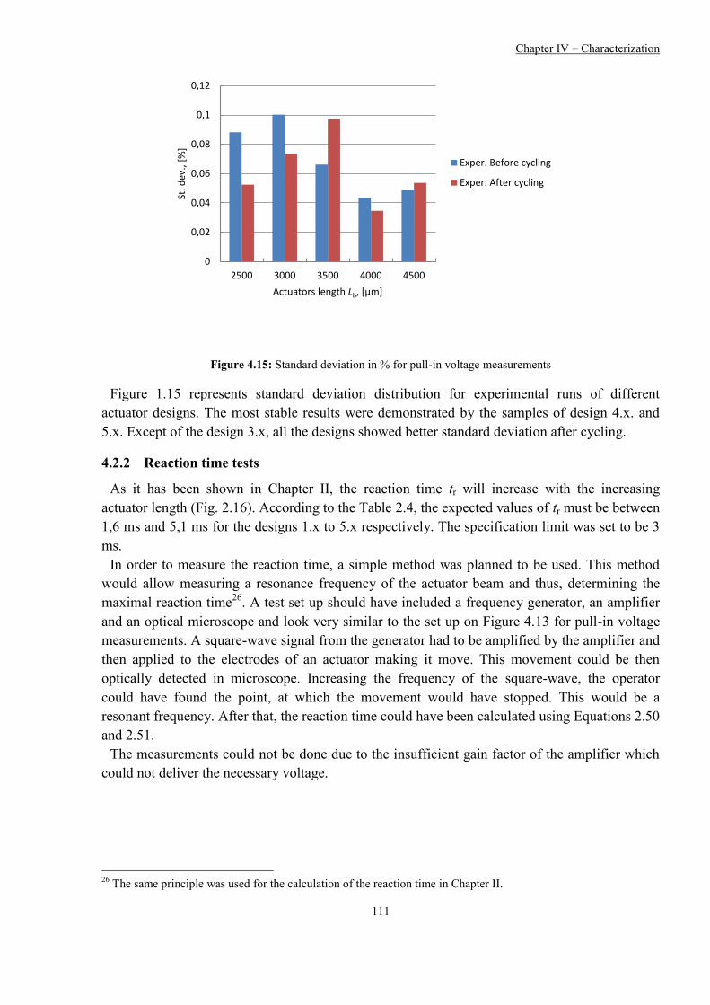
Chapter IV – Characterization
111
0
0,02
0,04
0,06
0,08
0,1
0,12
2500 3000 3500 4000 4500
St. d
ev.,
[%
]
Actuators length Lb, [µm]
Exper. Before cycling
Exper. After cycling
Figure 4.15: Standard deviation in % for pull-in voltage measurements
Figure 1.15 represents standard deviation distribution for experimental runs of different
actuator designs. The most stable results were demonstrated by the samples of design 4.x. and
5.x. Except of the design 3.x, all the designs showed better standard deviation after cycling.
4.2.2 Reaction time tests
As it has been shown in Chapter II, the reaction time tr will increase with the increasing
actuator length (Fig. 2.16). According to the Table 2.4, the expected values of tr must be between
1,6 ms and 5,1 ms for the designs 1.x to 5.x respectively. The specification limit was set to be 3
ms.
In order to measure the reaction time, a simple method was planned to be used. This method
would allow measuring a resonance frequency of the actuator beam and thus, determining the
maximal reaction time26
. A test set up should have included a frequency generator, an amplifier
and an optical microscope and look very similar to the set up on Figure 4.13 for pull-in voltage
measurements. A square-wave signal from the generator had to be amplified by the amplifier and
then applied to the electrodes of an actuator making it move. This movement could be then
optically detected in microscope. Increasing the frequency of the square-wave, the operator
could have found the point, at which the movement would have stopped. This would be a
resonant frequency. After that, the reaction time could have been calculated using Equations 2.50
and 2.51.
The measurements could not be done due to the insufficient gain factor of the amplifier which
could not deliver the necessary voltage.
26
The same principle was used for the calculation of the reaction time in Chapter II.
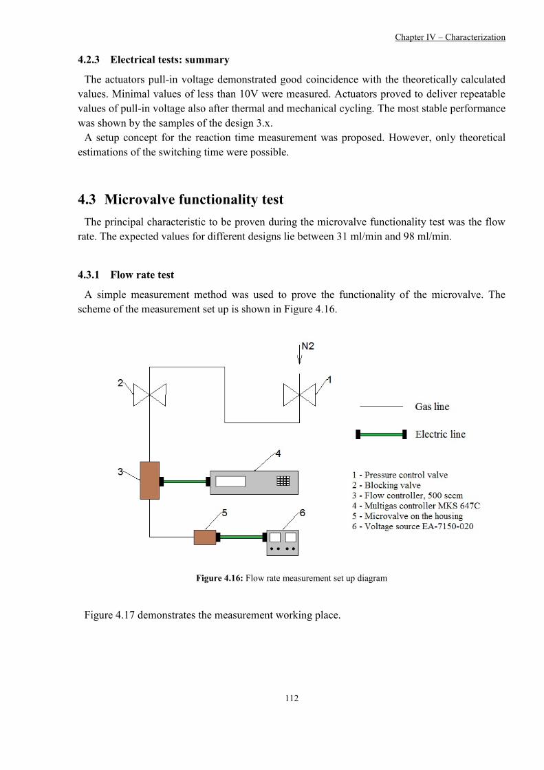
Chapter IV – Characterization
112
4.2.3 Electrical tests: summary
The actuators pull-in voltage demonstrated good coincidence with the theoretically calculated
values. Minimal values of less than 10V were measured. Actuators proved to deliver repeatable
values of pull-in voltage also after thermal and mechanical cycling. The most stable performance
was shown by the samples of the design 3.x.
A setup concept for the reaction time measurement was proposed. However, only theoretical
estimations of the switching time were possible.
4.3 Microvalve functionality test
The principal characteristic to be proven during the microvalve functionality test was the flow
rate. The expected values for different designs lie between 31 ml/min and 98 ml/min.
4.3.1 Flow rate test
A simple measurement method was used to prove the functionality of the microvalve. The
scheme of the measurement set up is shown in Figure 4.16.
Figure 4.16: Flow rate measurement set up diagram
Figure 4.17 demonstrates the measurement working place.

Chapter IV – Characterization
113
Figure 4.17: Flow rate measurement working place (pressure control valve (2) not shown)
The set up consisted of a flow controller, which limited the flow at 500 sccm, a multigas
controller MKS 647C to control the gas flow, pressure control valve to adjust the nominal
pressure, a blocking valve to open/close the gas flow, a voltage source to control the microvalve
and a microvalve on a housing/holder (Fig. 4.18). A microvalve sample chip was leak-proof
attached to the housing/holder using DELO “Katiobond 4557” (drying for 15 min. under 600W
UV-light). The housing/holder was specifically designed for the samples used in this work. The
technical drawing can be found in Appendix III.
Figure 4.18: A microvalve on a housing/holder
Nitrogen was used for the tests. The pressure of 2 bar was adjusted with the control valve (1).
Then the minimal gas flow value of 25 sccm and a maximal value of 250 sccm was adjusted on
the Multigas Controller MKS 647C (4). The values of the flow could then be changed within this

Chapter IV – Characterization
114
range. The actual values of the flow were then measured by the flow controller (3). Both
adjusted and measured values could be monitored on the screen of the Multigas Controller MKS
647C (4). The connections between the gas lines, devices and valves were sealed with
specialized sealing tape. For the measurements, only not cycled27
samples were used. For the
flow rate measurements, no voltage was applied to a microvalve sample leaving it open. In this
case the actual flow was that adjusted on the Multigas Controller. The adjustment was done with
the steps of 5 sccm: 25 sccm, 30 sccm etc… At the point, where the maximum allowable flow
through the valve was achieved, increase of the measured actual flow stopped. Similarly to the
previous measurements, five samples per design were measured. The results are represented in
Figure 4.19.
0
20
40
60
80
100
120
2000 2500 3000 3500 4000 4500 5000
Vo
lum
e fl
ow
Vfr
, [m
l/m
in]
Actuator length Lb, [µm]
Theor.
Exper.
Figure 4.19: Results of the flow rate measurement for different microactuator designs
The results show approximately 5 to 10 ml/min higher flow rates for all the designs. The reason
of this can be in a leakage somewhere in the measurement system. In order to prove, which of
the designs showed the most stable results, a standard deviation was calculated (Fig. 4.20).
27
No drop-tests, no temperature cycling

Chapter IV – Characterization
115
0,0%
2,0%
4,0%
6,0%
8,0%
10,0%
12,0%
14,0%
16,0%
18,0%
20,0%
2500 3000 3500 4000 4500
St. d
ev.,
[%
]
Actuator length Lb, [µm]
Figure 4.20: Standard deviation in % for microvalve flow rate measurements
For the designs 1.x and 2.x (Lb = 2500 µm and 3000 µm) very high standard deviations were
received meaning that the flow rate is unstable for those designs. The designs 3.x, 4.x and 5.x
showed better behavior, though standard deviations remained relatively high.
In order to prove the functionality of the valve in a closed state, a pull-in voltage was applied to
it as nitrogen was flowing through. The actual flow values dropped as the necessary voltages
were applied meaning the open/close function was performed.
4.3.2 Microvalve functionality test: summary
A gas-flow measurement setup was built in order to prove the ability of the microvalves to
deliver the calculated flows. The tests of microvalve functionality showed the results close to
theoretical ones (Fig. 4.19). Nevertheless, high values of standard deviation force the assumption
that either design, or calculations or rather measurement method and measurement set up must
be improved. It is assumed that for such a precise test, a vacuum chamber is needed, in which
leak-proof electrical connections and gas-lines must be foreseen.

Chapter V – Conclusion and suggestions for future research
116
5 Conclusions and suggestions for future research
In this work, a technological process for production of electrostatically driven curved
microactuator for pneumatic applications was presented. Using the process, fifteen design
variants of the microactuator integrated into a 2/2-microvalve chip were produced and then
characterized. The microvalve proved to deliver the flow rates up to 110±5 ml/min at differential
pressure of 2 bar and driving voltages of 11,6 V. As a basis for this work, a broad overview of
the existing microactuators and microvalves as well as the techniques of their production was
given.
During the design of the actuator, a model for the calculations of the mechanical and electrical
properties of the actuator was proposed. Basic microvalve performance was also estimated.
Electrostatic actuation principle was chosen for its good scaling properties to small dimensions,
low power consumption, smaller size and higher switching speed. Curved shape of the actuator
allowed to reduce the pull-in voltage and thus to increase the amplitude of motion as compared
to the parallel-plate structures.
Nickel was chosen as a material of the actuator for its good mechanical properties and relative
simplicity of processing. Double layer nickel electroplating was used to produce the
microactuator. The layers have different stress gradients controlled by current density during the
electroplating process, making it possible to achieve the desired bending of the structure.
Compared to bimetallic bending cantilever actuators, the curvature of the single-metal beam is
less dependable on temperature and aging. Thus, more stable performance under changing
working conditions was ensured. In order to avoid sticking of the microactuator to the isolation
layer in the closed state, an array of stand-off bumps was added on the back-side of the beam.
These bumps reduce the contact area and increase the distance between the actuator and the
isolation layer.
The technology developed in this work is a 6 photolithography layer process based on standard
4-inch Si substrates. But the possibility of alternative substrates utilization was also examined.
The study showed that though there are many materials, which could be readily used as
substrates (ceramics, FR-4, glass), from technological and financial point of view, Si remains the
best choice. The closest competitor could be Al2O3 ceramic (alumina). This material is very
widely used in industry; its costs are comparable with Si and it is available in a shape of wafers.
Moreover, ceramic is a natural insulator. This fact saves oxidation step and potentially reduces
the costs of the process. Thus, several types of Al2O3 of different purity were checked on their
technological suitability to the process developed in this work. Wet etching, photolithography
and electroplating with these substrates were studied. The studies revealed that there was no
simple and cheap way to remove ceramic material by wet etching, though some slow removal
took place in case of type Rubalit 708. Photolithography was in general possible, but the
alignment of a mask to the pattern on the substrate surface in the yellow room was very
problematic since no structures could be seen under the microscope even on the finest surface
with Ra = 0,1 µm. Electroplating revealed no problems and run as usually done with

Chapter V – Conclusion and suggestions for future research
117
conventional Si substrates. Summarizing the above mentioned facts, it was decided to go on
with Si substrates leaving ceramic for future R&D work.
The design of the technological flow was divided into three main phases:
- fabrication of a passive actuator (no bottom electrode)
- fabrication of an active actuator (with bottom electrode and contacts)
- process development for integration of the actuator into a microvalve
The first phase included several runs of subsequent surface micromachining steps focused on
electroplating and wet etching of sacrificial layers in order to check the reproducibility of the
deposition process and correspondence of the actuators final geometry to the theoretical
expectations.
During the second phase, bottom electrodes were added in order to make the actuator
functional. RIE dry etching method was developed to achieve well defined bottom electrodes.
In the last phase, a through silicon microchannel made by DRIE was introduced underneath the
actuator structure. All the separately developed flow steps were combined into a final
technological flow resulting in a 2/2 microvalve chip.
During characterization, mechanical stability of the actuators and microvalves as well as the
electrical performance and flow rates were studied. Mechanical robustness was examined by
means of drop, temperature and shear-tests. All the samples passed mechanical tests
successfully. Shear-tests of the microactuator showed good adhesion of the beams to the
underlying layers (up to 2 N) However, some weakening of the shear-force was observed after
thermal and drop-down cycling. Pull-in voltage was examined before and after temperature and
drop-down tests. The values of the pull-in voltage appeared to be slightly higher (approx. 0,5 –
0,6 V) for two design variants. It was proved that temperature and drop-down loads did not
significantly influence this parameter. The deflection of the actuator beams was measured before
and after thermal cycling and also showed the results comparable with theoretical expectations in
both cases. The measurements of the actuators reaction time could not be performed. But
theoretically calculated results lie in the region of 3 ms that corresponds to the specifications.
Measured flow rates of the microvalves (up to 110±5 ml/min) were also about 10 ml/min
higher than the expected theoretical ones. In this case, some leakage in the measurement system
was responsible for this offset.
The process and the system designed in this work resulted in a robust, effective and cheap
microactuator that could be integrated into a microvalve and provide performance comparable to
the similar systems reported in literature. However, the realization of the complete microvalve on
a single substrate can be seen as a step forward in comparison to the other systems. Moreover,
the process developed in this work possesses high flexibility and can be used not only for the
production of microvalves, but also for microrelays and other MEMS components.
Future research work must be concentrated on further examination of the alternative substrates
and higher effectiveness of the electroplating process. New electrode isolation materials and
actuator geometries can be investigated. The methods of system characterization must be
improved. System packaging concept should be developed.
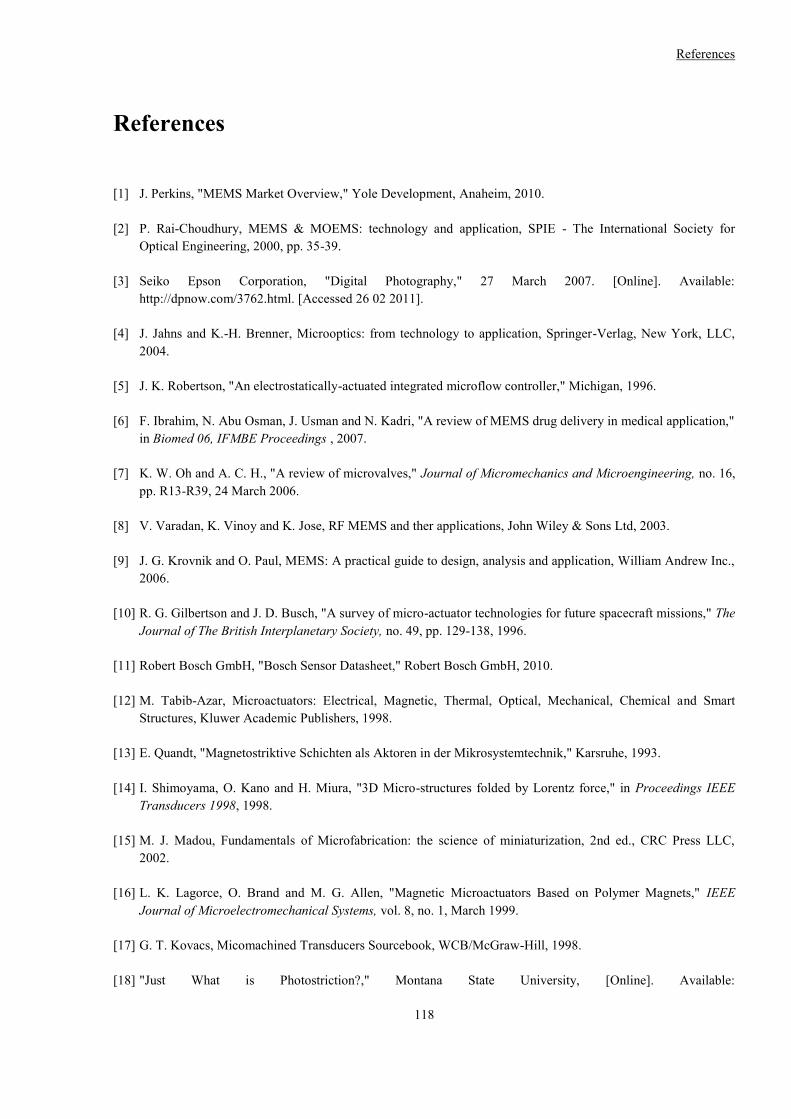
References
118
References
[1] J. Perkins, "MEMS Market Overview," Yole Development, Anaheim, 2010.
[2] P. Rai-Choudhury, MEMS & MOEMS: technology and application, SPIE - The International Society for
Optical Engineering, 2000, pp. 35-39.
[3] Seiko Epson Corporation, "Digital Photography," 27 March 2007. [Online]. Available:
http://dpnow.com/3762.html. [Accessed 26 02 2011].
[4] J. Jahns and K.-H. Brenner, Microoptics: from technology to application, Springer-Verlag, New York, LLC,
2004.
[5] J. K. Robertson, "An electrostatically-actuated integrated microflow controller," Michigan, 1996.
[6] F. Ibrahim, N. Abu Osman, J. Usman and N. Kadri, "A review of MEMS drug delivery in medical application,"
in Biomed 06, IFMBE Proceedings , 2007.
[7] K. W. Oh and A. C. H., "A review of microvalves," Journal of Micromechanics and Microengineering, no. 16,
pp. R13-R39, 24 March 2006.
[8] V. Varadan, K. Vinoy and K. Jose, RF MEMS and ther applications, John Wiley & Sons Ltd, 2003.
[9] J. G. Krovnik and O. Paul, MEMS: A practical guide to design, analysis and application, William Andrew Inc.,
2006.
[10] R. G. Gilbertson and J. D. Busch, "A survey of micro-actuator technologies for future spacecraft missions," The
Journal of The British Interplanetary Society, no. 49, pp. 129-138, 1996.
[11] Robert Bosch GmbH, "Bosch Sensor Datasheet," Robert Bosch GmbH, 2010.
[12] M. Tabib-Azar, Microactuators: Electrical, Magnetic, Thermal, Optical, Mechanical, Chemical and Smart
Structures, Kluwer Academic Publishers, 1998.
[13] E. Quandt, "Magnetostriktive Schichten als Aktoren in der Mikrosystemtechnik," Karsruhe, 1993.
[14] I. Shimoyama, O. Kano and H. Miura, "3D Micro-structures folded by Lorentz force," in Proceedings IEEE
Transducers 1998, 1998.
[15] M. J. Madou, Fundamentals of Microfabrication: the science of miniaturization, 2nd ed., CRC Press LLC,
2002.
[16] L. K. Lagorce, O. Brand and M. G. Allen, "Magnetic Microactuators Based on Polymer Magnets," IEEE
Journal of Microelectromechanical Systems, vol. 8, no. 1, March 1999.
[17] G. T. Kovacs, Micomachined Transducers Sourcebook, WCB/McGraw-Hill, 1998.
[18] "Just What is Photostriction?," Montana State University, [Online]. Available:

References
119
http://www.physics.montana.edu/eam/photostriction/photostriction.htm. [Accessed 25 March 2011].
[19] K. Uchino and J. R. Giniewicz, Micromechatronics, Marcel Dekker Inc., 2003.
[20] R. Maeda, J. Tsaur, S. Lee and M. Ichiki, "Piezoelectric Microactuator Devices," Journal of Electroceramics,
no. 12, pp. 89-100, 2004.
[21] A. Lee, D. Ciarlo, P. Krulevich, S. Lehew, J. Trevino and M. Northrup, "A Practical Microgripper by Fine
Alignment, Eutectic Bonding and SMA Actuation," in Proceedings of International Solid-State Sensors and
Actuators Conference (Transducers '95), Stockholm, Sweden, 1995.
[22] D. Bien, S. Mitchell and H. Gamble, "Fabrication and characterization of a micromachined passive valve,"
Journal of Micromechanics and Microengineering, no. 13, pp. 557-562, 14 May 2003.
[23] S. Terry, J. Jerman and A. J.B., "A gas chromatographic air analyzer fabricated on a silicon wafer," IEEE
Trans. Electron Devices, no. 26, pp. 1880-1886, 1979.
[24] K. Oh, A. Han, S. Bhansali and C. Ahn, "A low-temperature bonding technique using spin-on fluorocarbon
polymers to assemble microsystems," Journal of Micromechanics and Microengineering, no. 12, pp. 187-191,
2002.
[25] S. Shoji and E. Masayoshi, "Microflow devices and systems," Journal of Micromechanics and
Microengineering, no. 4, pp. 157-171, 1994.
[26] J. M. Park, "A piezoelectrically actuated cryogenic microvalve with integrated sensors," University of
Michigan, Michigan, 2009.
[27] T. Ohnstein, T. Fukiura, J. Ridley and U. Bonne, "Micromachined Silicon Microvalve," in Proceedings of
IEEE Workshop on Micro Electro Mechanical Systems, Napa Valley, CA, USA, 1990.
[28] X. Yang, A. Holke, S. Jacobson, J. Lang, S. M.A. and S. Umans, "An electrostatic, on/off microvalve designed
for gas fuel delivery for the MIT microengine," Journal of Microelectromechanical Systems, no. 13, pp. 660-
668, 2004.
[29] D. Roberts, H. Li, J. O. Steyn and S. Spearing, "A piezoelectric microvalve for compact high-frequency, high-
differential pressure hydraulic micropumping systems," Journal of Microelectromechanical Systems, no. 12,
pp. 81-92, 2003.
[30] T. Rogge, Z. Rummler and W. Schomburg, "Polymer micro valve with a hydraulic piezo-drive fabricated by
the AMANDA process," Sensors and Actuators, no. 110, pp. 206-212, 2004.
[31] P. Shao, Z. Rummler and W. Schomburg, "Polymer micro piezo valve with a small dead volume," Journal of
Micromechanics and Microengineering, no. 110, pp. 305-309, 2004.
[32] H. Jerman, "Electrically activated, normally closed diaphragm valves," Journal of Micromechanics and
Microengineering, no. 4, pp. 210-216, 1994.
[33] M. Zdeblick, "Thermopneumatically-Actuated Microvalves and Integrated Electrofluidic Circuits," in Solid-
State Sensor and Actuator Workshop, 1994.
[34] H. Takao, K. Miyamura, H. Ebi, M. Ashiki, K. Sawada and K. Ishida, "A MEMS microvalve with PDMS
diaphragm and two-chamber configuration of thermo-pneumatic actuator for integrated blood test system on

References
120
silicon," Sensors and Actuators, no. 119, pp. 468-475, 2005.
[35] C. Rich and K. Wise, "A high-flow thermopneumatic microvalve with improved efficiency and integrated state
sensing," Journal of Microelectromechanical Systems, no. 12, pp. 201-208, 2003.
[36] X. Yang, C. Grosjean and T. Y-C., "Design, fabrication, and testing of micromachined silicone rubber
membrane valves," Journal of Microelectromechanical Systems, no. 8, pp. 393-402, 1999.
[37] N.-T. Nguyen and S. T. Wereley, Fundamentals and applications of microfluidics, Artech House, Inc., 2002.
[38] M. Kohl, D. Dittmann, E. Quandt and B. Winzek, "Thin film shape memory microvalves with adjustable
operation temperature," Sensors and actuators, no. 83, pp. 214-219, 2000.
[39] P. Barth, "Silicon microvalves for gas flow control," in Proceedings 8th Int. Conf. on Solid-State Sensors and
Actuators (Transducers ’95), and Eurosensors IX, Stockholm, Sweden, 1995.
[40] C. Pemble and B. Towe, "A miniature shape memory alloy pinch valve," Sensors and Actuators, no. 77, pp.
145-148, 1999.
[41] I. Fazal, M. Louwerse, H. Jansen and M. Elwenspoek, "Stepper Motor Actuated Microvalve," Journal of
Physics: Conference Series, no. 34, pp. 1032-1037, 2006.
[42] C. Goll, W. Bacher, B. Büstgens, D. Maas, M. W. and W. Schomburg, "Microvalves with bistable buckled
polymer diaphragms," Journal of Micromechanics and Microengineering, no. 6, pp. 77-79, 1996.
[43] S. Bohm, G. Burger, M. Korthorst and F. Roseboom, "A micromachined silicon valve driven by a miniature bi-
stable electro-magnetic actuator," Sensors and Actuators, no. 80, pp. 77-83, 2000.
[44] D. Bosh, B. Heimhofer, G. Muck, H. Seidel, U. Thumser and W. Welser, "A silicon microvalve with combined
electromagnetic/electrostatic actuation," Sensors and Actuators, no. 37/38, pp. 684-692, 1993.
[45] D. Dissanayake and S. Al-Sarawi, "Designing remotely activated microvalves for biomedical applications,"
SPIE Newsroom, 2007.
[46] "Physorg.com," 20 May 2005. [Online]. Available: http://www.physorg.com/news4188.html. [Accessed 12
March 2011].
[47] "Wikipedia The free Encyclopedia," [Online]. Available: http://en.wikipedia.org/wiki/Coulomb's_law.
[Accessed 10 May 2011].
[48] V. Kaajakari, "MEMS Material," [Online]. Available:
http://www.kaajakari.net/~ville/research/tutorials/pull_in_tutorial.pdf. [Accessed 12 May 2011].
[49] D. Petrov, W. Lang and W. Benecke, "A nickel electrostatic curved beam actuator for valve applications," in
Proceedings Eurosensors XXIV, September 5-8, Linz, Austria, 2010.
[50] J. Schimkat, "Grundlagen und Modelle zur Entwicklung und Optimierung von Silizium-Mikrorelais," Berlin,
1996.
[51] M. Becker, "Entwurf einer Antriebsstruktur für ein MST-basiertes Mikrorelais zur Anwendung im Automobil,"
Bremen, 1999.

References
121
[52] "Wikipedia the Free Encyclopedia," [Online]. Available: http://en.wikipedia.org/wiki/Neutral_axis. [Accessed
14 May 2011].
[53] G. Gerlach and W. Dötzel, Grundlagen der Mikrosystemtechnik, München: Carl Hansen Verlag, 1997.
[54] Y. Hu, J. Yang and S. Kitipornchai, "Pull-in analysis of electrostatically actuated curved micro-beams with
large deformation," Smart Materials and Structures, no. 19, 17 May 2010.
[55] K.-S. Ou, K.-S. Chen, T.-S. Yang and S.-Y. Lee, "A Novel Semianalytical Approach for Finding Pull-In
Voltages of Micro Cantilever Beams Subjected to Electrostatic Loads and Residual Stress Gradients," Journal
of Microelectromechanical Systems, vol. 20, no. 2, pp. 527-537, 2011.
[56] C. W. Leow, M. Abu Bakar and M. K. Norazan, "Analytical Modeling For Determination Of Pull-In Voltage
For An Electrostatic Actuated MEMS Cantilever Beam," in ICSE2002 Proceedings, Penang, Malaysia, 2002.
[57] "Wikipedia the free Encyclopedia," [Online]. Available: http://en.wikipedia.org/wiki/Paschen's_law. [Accessed
01 June 2011].
[58] L. Germer, "Electrical breakdown between close electrodes in Air," Journal of Applied Physics, vol. 30, no. 1,
pp. 41-47, 1959.
[59] E. Clark, R. Yeske and H. Birnbaum, "The Effect of Hydrogen on the Surface Energy of Nickel,"
METALLURGICAL TRANSACTIONS A, vol. 11A, 1980.
[60] S. Timoshenko and S. Krieger, Theory of Plates and Shells, New York: McGraw-Hill, 1959.
[61] I. Voiculescu, M. E. Zaghloul, R. A. McGill, E. J. Houser and G. K. Fedder, "Electrostatically Actuated
Resonant Microcantilever Beam im CMOS Technology for the Detection of Chemical Weapons," IEEE Sensor
Journal, vol. 5, no. 4, 2005.
[62] M. Kampmann, "Theoretische Bestimmung der Geometrie- und Durflussparameter eines Mikroventils,"
Bremen, 2010.
[63] H. Sigloh, Technische Fluidmechanik, 6 ed., Springer, 2008.
[64] S. Messner, "Elektrostatisch angetriebenes 3/2-Wege-Mikroventil für pneumatische Anwendungen," Freiburg
im Breisgau, 2000.
[65] A. Henning, Interviewee, Personal communication. [Interview].
[66] "Richter Elektronik Handelsb[ro Heise, Produkte," [Online]. Available:
http://www.richterelektronik.de/prod_mx203.htm. [Accessed 03 September 2011].
[67] M. Köhler, Ätzverfahren für die Mikrotechnik, Wiley-VCH, 1998.
[68] B. Zhou and F. W. Ramirez, "Kinetics and Modeling of Wet Etching of Aluminum Oxide by Warm Phosphoric
Acid," Journal of Electrochemical Society, vol. 143, no. 2, pp. 619-623, 1996.
[69] D. Krell, Interviewee, Personal communication (e-mail). [Interview].
[70] A. Bödecker, Interviewee, Personal communication (e-mail). [Interview]. 23 April 2009.

References
122
[71] D. Petrov, "Prozessentwicklung für die Herstellung elektrostatischer Abrollaktoren für pneumatische
Mikroventile," Bremen, 2009.
[72] D. Petrov, "Modeling, fabrication and characterization of internal connections for bare die applications,"
Hamburg, 2006.

Appendix I
123
Acknowledgments
My warmest thanks go to Professor Dr.-Ing. Wolfgang Benecke for all of his help, support and
belief. I would also like to thank Professor Dr.-Ing. Walter Lang who provided a lot of advice
and support during my work on the project.
My very special thanks go to Azat Ibragimov whose share of experience and assistance were
invaluable especially for the theoretical calculations and practical work in a clean room. He also
helped me very much with some literature sources.
Additionally, I would like to acknowledge the technical assistance of Mohammad Shafi for his
help with electroplating and lithography, Ingrid Michels for her collaboration with samples
preparation and dicing. My thanks go also to Adam Sklorz for his friendly support and advise
every time it was needed.
I would like to thank all the team of the IMSAS for their kind collaboration and warm
atmosphere they created during my work.
Finally, I would like to say thank you to my wife, Kira, to my parents and friends for a positive
influence they all had on my attitude.

Appendix I
124
Appendix I
Photolithography masks
This appendix is a collection of the patterns used to produce foil photomasks. The patterns were
designed by the author. Due to the microscopically small size of some structures, not all of them
can be recognizable on the drawings.
Figure A1.1: Mask 1 Back-side alignment markings

Appendix I
125
Figure A1.2: Mask 2 Bottom electrodes

Appendix I
126
Figure A1.3: Mask 3 Gas-inlet channels

Appendix I
127
Figure A1.4: Mask 4 Anchor and electrodes openings

Appendix I
128
Figure A1.5: Mask 5 Stand-off bumps
Figure A1.6: Mask 5 Stand-off bumps (one structure magnified)
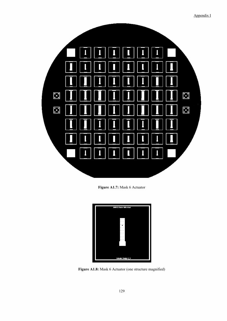
Appendix I
129
Figure A1.7: Mask 6 Actuator
Figure A1.8: Mask 6 Actuator (one structure magnified)

Appendix II
130
Appendix II
A map of microactuator design distribution over the waver
This Appendix contains a drawing explaining how the designs were distributed on the wafer
1_3 1_2 1_1 1_1 1_2 1_3
3_1 2_3 2_2 2_1 2_1 2_2 2_3 3_1
4_2 4_1 3_3 3_2 3_2 3_3 4_1 4_2
5_3 5_2 5_1 4_3 4_3 5_1 5_2 5_3
5_3 5_2 5_1 4_3 4_3 5_1 5_2 5_3
4_2 4_1 3_3 3_2 3_2 3_3 4_1 4_2
3_1 2_3 2_2 2_1 2_1 2_2 2_3 3_1
1_3 1_2 1_1 1_1 1_2 1_3
Figure A2.1: Microactuator designs distribution on the wafer

Appendix III
131
Appendix III
Microvalve housing/holder for flow rate measurements
This Appendix contains a technical drawing used by tool operators in the workshop to make a
housing/holder used to characterize the flow rate of a microvalve.

Appendix III
132
Figure A3.1: Microvalve housing/holder for flow rate measurements
List of figures
133
List of figures
Figure 1.1: Airbag control system (left) and acceleration sensor in a package (right) [5] ............................................. 2
Figure 1.2: Current and future MEMS sensor applications in a car [2] ......................................................................... 3
Figure 1.3: Cross-section of a print-head [3] ................................................................................................................. 3
Figure 1.4: The GeneExpert cartridge with a rotary valve for sample preparation and real-time PCR [8] .................. 4
Figure 1.5: Bulk (left) and surface (right) micromachining sequences ......................................................................... 5
Figure 1.6: Schematic of an actuator function. .............................................................................................................. 7
Figure 1.7: Heat conduction in a solid between two plates at different temperatures. ................................................ 11
Figure 1.8: Schematic representation of a bimorph actuation principle. ..................................................................... 13
Figure 1.9: Surgical SMA microgripper [21] .............................................................................................................. 16
Figure 1.10: Check valve concept [22]. ....................................................................................................................... 17
Figure 1.11: Actuation principles of active mechanical microvalves: (a) electromagnetic; (b) electrostatic; ............. 18
Figure 1.12: The microvalve with a solenoid plunger by Terry et al. [23] .................................................................. 18
Figure 1.13: Magnetic microvalve with an integrated magnetic inductor by Oh et al. [24] ........................................ 19
Figure 1.14: Electrostatic fuel valve [28] .................................................................................................................... 20
Figure 1.15: A concept of microvalve with an S-shaped electrostatic microactuator.................................................. 20
Figure 1.16: A concept of a piezoelectrically actuated microvalve with stacked PZT [26] ....................................... 21
Figure 1.17: Cross section of a bimetallically actuated diaphragm microvalve [32] ................................................... 22
Figure 1.18: The thermopneumatic microvalve with composite ................................................................................. 23
Figure 1.19: A normally closed SMA microvalve with external metal spring [33] .................................................... 23
Figure 1.20: Schematic cross-section of a thin film SMA microvalve [39] ................................................................ 24
Figure 1.21: A stepper-motor actuated microvalve [41] .............................................................................................. 25
Figure 1.22: The bistable electromagnetic microvalve with an integrated magnet [43] .............................................. 25
Figure 1.23: Thermopneumatic microvalve and its working principle (adapted from [15]) ....................................... 27
Figure 1.24: A distributed cooling system concept [26] .............................................................................................. 28
Figure 1.25: A general representation of a curved beam actuator for a microvalve. ................................................... 30
Figure 2.1: The mechanism of electrostatic interaction. .............................................................................................. 32
Figure 2.2: Parallel plate capacitor. ............................................................................................................................. 33

List of figures
134
Figure 2.3: Schematic of an electrostatic actuator. ...................................................................................................... 34
Figure 2.4: Microactuator mechanical concept [49] .................................................................................................... 36
Figure 2.5: The electrical working principal of the curved beam electrostatic microatuator ...................................... 37
Figure 2.6: Actuators bending curve as a result of internal stress gradient and external electrostatic force ............... 37
Figure 2.7: Neutral axis in a beam of j layers .............................................................................................................. 40
Figure 2.8: Mechanical stresses inside a multilayered beam ....................................................................................... 41
Figure 2.9: Breakdown voltage vs. gas pressure [57] .................................................................................................. 44
Figure 2.10: Static deflection of the double layered nickel actuator ........................................................................... 50
Figure 2.11: Actuator static deflection vs. layer thickness ratio .................................................................................. 51
Figure 2.12: Pull-in voltage vs. actuator length ........................................................................................................... 52
Figure 2.13: Pull-in voltage vs. layer thickness ratio. Lb = 3000 µm, b = 500 µm ...................................................... 52
Figure 2.14:Pull-in voltage vs minimal gap. Lb = 3000 µm, b = 500 µm .................................................................... 53
Figure 2.15: Graphical estimation of the pull-in voltage by static and electrostatic deflection ................................... 53
Figure 2.16: Actuators reaction time vs. beam length and layer thickness ratio ......................................................... 54
Figure 2.17: Schematic representation of the gas flow through the orifice ................................................................. 57
Figure 2.18: Qualitative representation of the outflow function. ................................................................................. 58
Figure 2.19: On the influence of the channel geometry on the gas flow (adapted from [62]) ..................................... 60
Figure 2.20: Position of the actuator above the gas inlet channel ............................................................................... 62
Figure 2.21: To the calculation of the smean ................................................................................................................. 62
Figure 2.22: A cross-sectional view of a microvalve chip with basic dimensions (not to scale)................................. 64
Figure 2.23: Volume flow rate as a function of inlet pressure at different channel diameters .................................... 65
Figure 2.24: Volume flow as a function of inlet pressure at different valve lifts ........................................................ 65
Figure 2.25: Forces acting on the actuator’s beam in the pulled-in state ..................................................................... 66
Figure 2.26: Comparison of forces acting on the actuator's beam in a pulled-in state (Upi = 12 V) ............................ 67
Figure 3.1: Wafer geometry gauge Eichhorn & Hausmann MX-203 [66] .................................................................. 72
Figure 3.2: Ni layer stress vs. current density at layer thickness from 2.4 to 3 µm ..................................................... 73
Figure 3.3: Ni layer stress vs. current density at layer thickness from 5.5 to 6 µm ..................................................... 73
Figure 3.4: Contact thickness measurement points on the substrate. .......................................................................... 77
Figure 3.5: Graphical representation of the etching results in PWS. .......................................................................... 77
Figure 3.6: Graphical representation of the etching results in H3PO4. ....................................................................... 77

List of figures
135
Figure 3.7: KER710 Substrates covered with patterned chromium layer: .................................................................. 79
Figure 3.8: Broken CeramTec Rubalit 710 substrate covered with chromium mask .................................................. 80
Figure 3.9: Alumina KER 708 91% covered with TI35 photoresist mask .................................................................. 81
Figure 3.10: The released actuators on the alumina substrate ..................................................................................... 82
Figure 3.11: First design of a borosilicate glass photomask for bottom electrodes ..................................................... 84
Figure 3.12: Passive microactuator production flow ................................................................................................... 85
Figure 3.13: Wet etched cavity for a stand-off bump in a Cu layer:............................................................................ 86
Figure 3.14: Chrome underetching in Chrom-Etch 3144 after 10 sec. dip .................................................................. 88
Figure 3.15: Chrome underetching in "Chrom-Etch 3144": thin structure destroyed ................................................. 88
Figure 3.16: Resist ashes on the Cr electrodes surface after Ar-plasma etching ......................................................... 90
Figure 3.17: Dry etched Cr/Au/Cr electrodes: etching with thermal paste .................................................................. 91
Figure 3.18: Etching result of a Cr/Au/Ti electrode. ................................................................................................... 91
Figure 3.19: Microvalve flow: thermal oxidation ........................................................................................................ 94
Figure 3.20: Microvalve flow: back side alignment markings .................................................................................... 94
Figure 3.21: Microvalve flow: adhesion and bottom electrodes layer ......................................................................... 94
Figure 3.22: Microvalve flow: structured bottom electrodes....................................................................................... 95
Figure 3.23: Microvalve flow: DRIE of gas inlet channels ......................................................................................... 95
Figure 3.24: Microvalve flow: PECVD of Si3N4 isolation ......................................................................................... 96
Figure 3.25: Gas inlet from the top side ...................................................................................................................... 96
Figure 3.26: Microvalve flow: PVD of Ti/Cu sacrificial layer .................................................................................... 96
Figure 3.27: Microvalve flow: wet etching, ................................................................................................................ 97
Figure 3.28: Microvalve flow: Ni electroplating ......................................................................................................... 97
Figure 3.29: Microvalve flow: back side etching of the SiO2/Si3N4 membrane .......................................................... 97
Figure 3.30: Microvalve flow: actuator release ........................................................................................................... 98
Figure 3.31: Electrically disconnected electrodes after Ti/Cu etching ........................................................................ 98
Figure 3.32: Fabricated microactuator on a chip (REM representation) ..................................................................... 98
Figure 4.1: Shear test diagram (not to scale) ............................................................................................................. 101
Figure 4.2: Shear test setup with XYZTEC Condor 100 tool .................................................................................... 102
Figure 4.3: Failure force for different actuator designs ............................................................................................. 103
Figure 4.4: Standard deviation of the failure measurement for differnt actuator designs .......................................... 103
List of figures
136
Figure 4.5: Remains of the sacrificial layer (actuator removed)................................................................................ 104
Figure 4.6: Typical half sinusoidal form of the deceleration vs. time (adapted from [72]) ....................................... 105
Figure 4.7: Scheme of a drop test set up .................................................................................................................... 106
Figure 4.8: Thermal cycling set up ............................................................................................................................ 107
Figure 4.9: Thermal cycling temperature profile ....................................................................................................... 107
Figure 4.10: Deflection of the actuator s before and after thermal cycling compared with theory ........................... 108
Figure 4.11: Standard deviation in % of the beam deflection measurements ............................................................ 108
Figure 4.12: Microvalve chip on a circuit board ready for electrical tests ................................................................ 109
Figure 4.13: Pull-in voltage test set up ...................................................................................................................... 110
Figure 4.14: Pull-in voltage measured for different actuator designs ........................................................................ 110
Figure 4.15: Standard deviation in % for pull-in voltage measurements ................................................................... 111
Figure 4.16: Flow rate measurement set up diagram ................................................................................................. 112
Figure 4.17: Flow rate measurement working place (pressure control valve (2) not shown) .................................... 113
Figure 4.18: A microvalve on a housing/holder ........................................................................................................ 113
Figure 4.19: Results of the flow rate measurement for different microactuator designs ........................................... 114
Figure 4.20: Standard deviation in % for microvalve flow rate measurements ......................................................... 115
Figure A1.1: Mask 1 Back-side alignment markings ................................................................................................ 124
Figure A1.2: Mask 2 Bottom electrodes .................................................................................................................... 125
Figure A1.3: Mask 3 Gas-inlet channels ................................................................................................................... 126
Figure A1.4: Mask 4 Anchor and electrodes openings .............................................................................................. 127
Figure A1.5: Mask 5 Stand-off bumps ...................................................................................................................... 128
Figure A1.6: Mask 5 Stand-off bumps (one structure magnified) ............................................................................. 128
Figure A1.7: Mask 6 Actuator ................................................................................................................................... 129
Figure A1.8: Mask 6 Actuator (one structure magnified) ......................................................................................... 129
Figure A2.1: Microactuator designs distribution on the wafer .................................................................................. 130
Figure A3.1: Microvalve housing/holder for flow rate measurements ...................................................................... 132
List of tables
137
List of tables
Table 1.1 IC and MEMS Processes and materials ......................................................................................................... 6
Table 1.2: Comparison of basic microvalve principles and their properties................................................................ 26
Table 2.1: Classification of basic parameters for actuator's dimensioning .................................................................. 49
Table 2.2: Actuator geometry design variations .......................................................................................................... 55
Table 2.3: Properties of N2 and air at normal conditions ............................................................................................ 56
Table 2.4: Summary of the calculated parameters for different actuator design variants ............................................ 68
Table 3.1: Ni layer stress measurement order. Wafers 1 to 12 .................................................................................... 71
Table 3.2: Ni layer stress measurement order. Wafers 13 to 20 .................................................................................. 71
Table 3.3: Wet etching experimental setups ................................................................................................................ 76

Declaration
138
Declaration
Herewith, I assure that present work has been done independently, with use of listed literature
sources and additional materials.
Denis A. Petrov
Pinneberg, March 2012