DESIGN AND IMPLEMENTATION OF COMBINED PIPELINING AND...
16
International Journal of VLSI design & Communication Systems (VLSICS) Vol 10, No 4, August 2019 DOI : 10.5121/vlsic.2019.10401 1 DESIGN AND IMPLEMENTATION OF COMBINED PIPELINING AND P ARALLEL PROCESSING ARCHITECTURE FOR FIR AND IIR FILTERS USING VHDL Jacinta Potsangbam 1 and Manoj Kumar 2 1 M. Tech VLSI Design, Dept. of ECE, National Institute of Technology, Manipur, India 2 Assistant Professor, Dept. of ECE, National Institute of Technology, Manipur, India ABSTRACT Along with the advancement in VLSI (Very Large Scale Integration) technology, the implementation of Finite impulse response (FIR) filters and Infinite impulse response (IIR) filters with enhanced speed has become more demanding. This paper aims at designing and implementing a combined pipelining and parallel processing architecture for FIR and IIR filter using VHDL (Very High Speed Integrated Circuit Hardware Descriptive Language) to reduce the power consumption and delay of the filter. The proposed architecture is compared with the original FIR and IIR filter respectively in terms of speed, area, and power. Also, the proposed architecture is compared with existing architectures in terms of delay. The implementation is done by using VHDL codes. FIR and IIR filters structures are implemented at 1200 KHz clock frequency. Synthesis and simulation have been accomplished on Artix-7 series FPGA, target device (xc7a200tfbg676) (speed grade -1) using VIVADO 2016.3. KEYWORDS DSP, FIR, FPGA, IIR, MIMO. 1. INTRODUCTION A filter is one of the basic signal processing circuits used in communication systems and physical applications. Filters are the electronic circuits which allow or transmit the desired band of frequencies and attenuate the unwanted band of frequencies. Digital filters process and generate digital data. Digital filters consist of elements like adder, multiplier and delay unit. The properties of a causal digital filter can be completely characterized by its unit-sample response h(n), or its transfer function H(z), or by difference equations [1]. Difference equation representations definitely show the computations required to implement the filter. The transfer function for a linear, causal and time-invariant, digital filter can be expressed as a transfer function in the z- domain as: 1 2 0 1 2 1 2 1 2 ... () () () 1 ... N N M M b bz bz bz Bz Hz Az az az a z (1) Where the order of the filter should be greater than N or M. In discrete-time systems, the digital filter is often implemented by converting the transfer function to a linear difference equation. The resultant linear difference equation is: [2]
Transcript of DESIGN AND IMPLEMENTATION OF COMBINED PIPELINING AND...
International Journal of VLSI design & Communication Systems (VLSICS) Vol 10, No 4, August 2019
DOI : 10.5121/vlsic.2019.10401 1
DESIGN AND IMPLEMENTATION OF COMBINED
PIPELINING AND PARALLEL PROCESSING
ARCHITECTURE FOR FIR AND IIR FILTERS USING
VHDL
Jacinta Potsangbam1 and Manoj Kumar2
1M. Tech VLSI Design, Dept. of ECE, National Institute of Technology, Manipur, India
2Assistant Professor, Dept. of ECE, National Institute of Technology, Manipur, India
ABSTRACT
Along with the advancement in VLSI (Very Large Scale Integration) technology, the implementation of
Finite impulse response (FIR) filters and Infinite impulse response (IIR) filters with enhanced speed has
become more demanding. This paper aims at designing and implementing a combined pipelining and
parallel processing architecture for FIR and IIR filter using VHDL (Very High Speed Integrated Circuit
Hardware Descriptive Language) to reduce the power consumption and delay of the filter. The proposed
architecture is compared with the original FIR and IIR filter respectively in terms of speed, area, and
power. Also, the proposed architecture is compared with existing architectures in terms of delay. The
implementation is done by using VHDL codes. FIR and IIR filters structures are implemented at 1200 KHz
clock frequency. Synthesis and simulation have been accomplished on Artix-7 series FPGA, target device
(xc7a200tfbg676) (speed grade -1) using VIVADO 2016.3.
KEYWORDS
DSP, FIR, FPGA, IIR, MIMO.
1. INTRODUCTION
A filter is one of the basic signal processing circuits used in communication systems and physical
applications. Filters are the electronic circuits which allow or transmit the desired band of
frequencies and attenuate the unwanted band of frequencies. Digital filters process and generate
digital data. Digital filters consist of elements like adder, multiplier and delay unit. The properties
of a causal digital filter can be completely characterized by its unit-sample response h(n), or its
transfer function H(z), or by difference equations [1]. Difference equation representations
definitely show the computations required to implement the filter. The transfer function for a
linear, causal and time-invariant, digital filter can be expressed as a transfer function in the z-
domain as:
1 2
0 1 2
1 2
1 2
...( )( )
( ) 1 ...
N
N
M
M
b b z b z b zB zH z
A z a z a z a z
(1)
Where the order of the filter should be greater than N or M.
In discrete-time systems, the digital filter is often implemented by converting the transfer function
to a linear difference equation. The resultant linear difference equation is: [2]

International Journal of VLSI design & Communication Systems (VLSICS) Vol 10, No 4, August 2019
2
1 0
( ) ( ) ( )N M
k k
k k
y n a y n k b x n k
(2)
High-performance digital filter is the need for digital signal processing. The speed of a filter
realization depends not only on the potentialities of the hardware platform on which it is
employed, but as well on the computational structure of the code [3].
The objective of the paper is to design and implement a combined pipelining and parallel
processing architectures on FIR and IIR digital filters to achieve high-speed or low power
consumption.
This paper is organized as follows: In Section 2 and 3, the FIR and IIR filter are discussed.
Pipelining and parallel processing techniques are discussed in Section 4 and 5. In Section 6,
literature survey is presented. In Section 7, implementation of the combined pipelining and
parallel processing is discussed. Simulation results and performance analysis of the implemented
architectures are discussed in sections 8 and 9. Conclusions are given in Section 10.
2. FIR FILTER
The FIR digital filter is widely used in DSP systems, ranging from wireless communications to
video and image processing [4]. FIR filters are non-recursive filters as there is no feedback
involved. All paths connecting the input to the output flows in the forward direction, so the signal
flow is strictly feed-forward in FIR Filter.
The difference equation for the FIR filter which defines the relation of the input signal to the
output signal is given as
0 1( ) ( ) ( 1) ... ( )Ny n b x n b x n b x n N (3)
It can also be expressed as
0
( ) ( )N
i
i
y n b x n i
(4)
Where x(n) is the input signal, y(n) is the output signal, bi is the filter coefficients and N is the
filter order [5].
In an FIR filter, DSP microprocessors feature multiply-accumulate (MAC) units since adders for
additions are required in combination with multiplier for the multiplications. Based on the
multiplication and accumulation of filter coefficients, the accuracy of designing a filter is
determined. FIR filters are the causal, linear and time-invariant systems.
The realization of FIR filter in transpose form configuration is required. Transpose form FIR
filter preserves the functionality of the filter and overcomes the computational delay problem of
the direct form FIR Filter [6].
International Journal of VLSI design & Communication Systems (VLSICS) Vol 10, No 4, August 2019
3
3. IIR FILTER
IIR filters have feedback loop (a recursive part of a filter) so they are also called as recursive
filters. The difference equation for IIR filter that defines how the output signal is related to the
input signal is given as
0 10
1( ) ( ) ( )
QP
i j
i j
y n b x n i a y n ja
(5)
The transfer function is defined as
1
0
1
0
( )( )
( )
P
ii
Q
jj
b zY zH z
X z a z
(6)
Considering that in most IIR filter designs coefficient a0 is 1, the IIR filter transfer function can
be rewritten as
1
0
1
1
( )( )
( ) 1
P
ii
Q
jj
b zY zH z
X z a z
(7)
where P is the feed-forward filter order, bi is the feed-forward filter coefficients, Q is the feedback
filter order, ajis the feedback filter coefficients, x(n) is the input signal and y(n) is the output
signal [7].
IIR filters are better to implement than FIR filters to meet the specifications like pass band, stop
band, etc. Computation time is saved by using digital IIR filters which is a large factor. IIR filters
are computationally more efficient than FIR filters as they require fewer coefficients due to the
usage of poles and feedback [21].
4. PIPELINING
Pipelining is an implementation technique where a stream of instructions are executed
simultaneously and results in speed enhancement for the critical path by reducing the critical path
delay in most of the DSP system [8]. Pipelining accumulates the instructions from the processor
making the processors fast [5]. By using pipelining technique, critical path can be reduced, which
in turn increases the sample speed and throughput of the system. It can also be used to reduce
power consumption at the same speed [1] [4].

International Journal of VLSI design & Communication Systems (VLSICS) Vol 10, No 4, August 2019
4
Figure 1. Fine-grain pipelining of a 3-tap FIR filter.
In the FIR filter, the pipeline latches are introduced across any feed-forward cutset without
changing the transfer function at the expense of latency. This is referred to as fine-grain
pipelining. Figure 1 shows a fine-grain pipelining of a 3-tap FIR filter. In an M-level pipelined
system, the number of delay elements in any path from input to output is (M-1) greater than the
delay element in the original sequential circuit [1].
In IIR filter, simply inserting pipelining latches alter the loop delay which leads to a change in the
transfer function. Hence, in order to pipeline an IIR filter while conserving its original transfer
function, the computations must first be redeveloped into what is called a look-ahead filter
form[5][9]. IIR filters are pipelined using look-ahead techniques and decomposition technique
which is discussed in [10]. This reformulation provides additional delays in the feedback loop
that can be used to balance the pipeline stages by introducing a new cancelling pole and zero for
each additional register inserted.
Pipelining does not accelerate instruction execution time, but it does accelerate program
execution time by increasing the number of instructions finished per unit time [5] [8] [4].
There is a limitation in pipelining which is imposed by the input/output (I/O) bottlenecks. This
essentially means that pipelining can be used only to the extent such that the critical path
computation time is limited by the communication or I/O bound, and once the system is
communication bounded, pipelining can no longer increase the speed of the system. Once the
system is communication bounded, pipelining can be combined with parallel processing to further
increase the speed of the architecture [1].
5. PARALLEL PROCESSING
Parallel processing is an implementation technique in which multiple outputs are computed in
parallel in a clock period. In parallel processing, the hardware for the original serial system is
duplicated and the resulting system is a MIMO (multiple inputs multiple outputs) parallel system.
Figure 2 shows the block diagram of conversion of SISO (single input single output) system to a
MIMO system.
Figure 2. Sequential system to 3-parallel system.
International Journal of VLSI design & Communication Systems (VLSICS) Vol 10, No 4, August 2019
5
Parallel processing systems are also referred to as block processing systems. Because of the
MIMO system, placing a latch at any path produces a delay of L clock cycles. In the block
structure with block size L, each implementable latch is L-slow, i.e., the clock rate of the latch in
the block filter is L times slower than the input sample rate. If an L parallel filter is operated, L
output samples are generated every clock period whereas in the original filter single output
sample is generated in every clock period. This implies that the L-parallel filter effectively
operates at L times the rate of the original filter [11] [12]. In parallel filter, the sampling
frequency is increased while the frequency of the clock remains the same. Therefore, the effective
sampling speed of the system is increased by the level of parallelism [1].
Parallel processing is a robust technique because it can be used to increase the throughput of a
digital filter or to reduce the power consumption of a digital filter [11] [13]. The block processing
method not only increases the throughput of the system but also improves area-delay efficiency.
In IIR filter, in straightforward implementation of parallel processing, the hardware complexity is
L2 multiply-add operations since L multiply-add operations are required for each output and there
are L outputs in total. The incremental block processing technique can be used to reduce
hardware complexity. In the incremental computation, the outputs are incrementally computed in
a sequential manner using the non-recursively computed intermediate states [14]. The hardware
complexity has been reduced to 2L −1 from L2at the expense of an increase in the system latency
[1].
Parallel processing is used for the reduction of power consumption while using slow clocks. This
reduces the power consumption due to the clock lines as compared with a pipelined system,
which needs to be operated using a faster clock for equivalent throughput or sample speed.
6. RELATED WORK
In [5], the author uses the technique of pipelining to measure the efficiency of an algorithm. The
author uses different FPGAs to perform a comparative study between pipelined & non-pipelined
FIR and IIR filters. The results show that the implemented pipelined filter improves the overall
speed of the filter than the non-pipelined filter. In [20], for high throughput applications, the
author implemented four different structures: unfolded direct form parallel
architectures(UDFPA), unfolded broadcast form parallel architectures(UBFPA), parallel retimed
broadcast architecture (PRBA) and parallel systolic architecture (PSA) with varying levels of
parallel and pipelined implementations of finite impulse response (FIR) filter using different
FPGAs. The author concluded that PSA has a better resource utilization based in terms of area-
delay product and power-delay product. In [3], the author proposes an FPGA based design of
exceedingly high-speed notch filter which practically operates at a maximum clock frequency of
1200MHz using Scattered-Look-Ahead (SLA) pipelining with a power-of-2-decomposition
approach. The author also proposes a new efficient simpler approach for calculating the
coefficients of the multiplier of both feed-forward and feedback portions of an exceedingly high-
speed notch filter using Pascal’s Triangle. The proposed work is applicable in communication as
well as in the non-communication field where noise elimination is necessary.In [19], a 4-tap
sequential and parallel micro-programmed based digital FIR filter have been implemented with
the help of a 16 bit Wallace tree multiplier and a 16 bit Vedic multiplier using VHDL codes.
Based on the implementation results obtained through FPGA synthesis tools performance of the
filter is evaluated. The author observes that the sequential filter achieves better performance with
reference to speed and resource utilization than the parallel filter. Also, Vedic multiplier is faster
than Wallace multiplier.

International Journal of VLSI design & Communication Systems (VLSICS) Vol 10, No 4, August 2019
6
7. PROPOSED WORK
7.1. Implementation of 3-Tap FIR Filter
The difference equation of the 3-tap FIR filter can be expressed as
( ) ( ) ( 1) ( 2)y n ax n bx n cx n (8)
Figure 3. Direct form 3-tap FIR Filter [1].
Figure 4. Transposed form 3-tap FIR Filter [1].
The direct form structure and transposed form structure of 3-tap FIR filter is shown in Figure 3
and Figure 4 respectively. The transposed form 3-tap FIR filter is implemented at 1200 kHz
frequency using VHDL codes. The 1200 kHz clock frequency is derived from the system
frequency of 50 MHz.
7.2. Implementation of Combined Parallel-Pipelined FIR Filter
The parallel structure of the 3-tap FIR filter is shown in Figure 5.
Figure 5. Parallel structure for 3-tap FIR filter [1].
The difference equation of the parallel FIR is

International Journal of VLSI design & Communication Systems (VLSICS) Vol 10, No 4, August 2019
7
2 0 1
1 2 0
0 1 2
(3 ) (3 ) (3 2) (3 1)
(3 1) (3 ) (3 1) (3 1)
(3 2) (3 ) (3 1) (3 2)
y k h x k h x k h x k
y k h x k h x k h x k
y k h x k h x k h x k
For implementing a combined parallel-pipelined structure, the sequential system is converted into
a parallel system by using a serial to parallel converter. In a MIMO system the inputs are
generated using the 3600 kHz frequency clock. The multiplier in the parallel structure is broken
into two smaller units by fine grain pipelining. This parallel-pipelined structure is implemented
using VHDL codes at 1200 kHz clock frequency. Here, the level of parallelism used is 3 and that
of pipelining is 2. Hence, three outputs are generated in every clock cycle.
Combined pipelined and parallel processing architecture for 3-tap FIR filter is shown in Figure 6.
Figure 6. Combined pipelined and parallel processing architecture for 3-tap FIR filter.
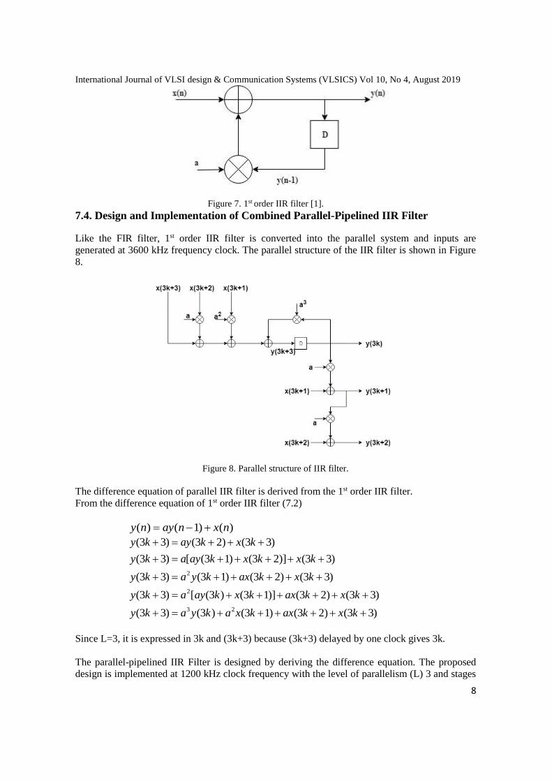
7.3. Implementation of 1st Order IIR Filter
Since it is 1st order IIR filter, it has only one pole at ‘a’. The value of |a| should be less than or
equal to 1 for the system to be stable (here the value of a is assumed to be 0.5).
( ) ( 1) ( )y n ay n x n (9)
It can also be expressed as
( ) 0.5 ( 1) ( )y n y n x n
From the difference equation, the 1st order IIR filter is implemented at 1200 kHz clock using
VHDL codes. Figure 7 shows the block diagram of the 1st order IIR filter.
International Journal of VLSI design & Communication Systems (VLSICS) Vol 10, No 4, August 2019
8
Figure 7. 1st order IIR filter [1].
7.4. Design and Implementation of Combined Parallel-Pipelined IIR Filter
Like the FIR filter, 1st order IIR filter is converted into the parallel system and inputs are
generated at 3600 kHz frequency clock. The parallel structure of the IIR filter is shown in Figure
8.
Figure 8. Parallel structure of IIR filter.
The difference equation of parallel IIR filter is derived from the 1st order IIR filter.
From the difference equation of 1st order IIR filter (7.2)
( ) ( 1) ( )y n ay n x n
2
2
3 2
(3 3) (3 2) (3 3)
(3 3) [ (3 1) (3 2)] (3 3)
(3 3) (3 1) (3 2) (3 3)
(3 3) [ (3 ) (3 1)] (3 2) (3 3)
(3 3) (3 ) (3 1) (3 2) (3 3)
y k ay k x k
y k a ay k x k x k
y k a y k ax k x k
y k a ay k x k ax k x k
y k a y k a x k ax k x k
Since L=3, it is expressed in 3k and (3k+3) because (3k+3) delayed by one clock gives 3k.
The parallel-pipelined IIR Filter is designed by deriving the difference equation. The proposed
design is implemented at 1200 kHz clock frequency with the level of parallelism (L) 3 and stages

International Journal of VLSI design & Communication Systems (VLSICS) Vol 10, No 4, August 2019
9
of pipelining (M) 2. The inputs are generated at 3600 kHz clock. Figure 9 shows the combined
pipelining and parallel processing architecture for IIR filter.
From the difference equation of the 1st order IIR filter (7.2)
( ) ( 1) ( )y n ay n x n
Since M=2, we have to add one more delay to the original sequential filter and L=3, hence (3k).
So (3k+6) delayed by two cycles gives (3k).
Therefore,
(3 1) (3 ) (3 1)
(3 2) (3 1) (3 2)
.
.
(3 5) (3 4) (3 5)
(3 6) (3 5) (3 6)
y k ay k x k
y k ay k x k
y k ay k x k
y k ay k x k
Substituting the values, we get
6 5 4 3 2(3 6) (3 ) (3 1) (3 2) (3 3) (3 4) (3 5) (3 6)y k a y k a x k a x k a x k a x k ax k x k
Figure 9. Combined pipelined and parallel processing architecture for 1st order IIR filter.
The proposed combined pipelining and parallel processing architecture for IIR Filter is designed
and implemented.
The results of the implemented designs are being analyzed in the latter section of this paper.

International Journal of VLSI design & Communication Systems (VLSICS) Vol 10, No 4, August 2019
10
8. EXPERIMENTAL RESULTS
The register transfer level (RTL) schematic of 3-tap FIR filter is shown in Figure 10. The
simulation output waveform of the 3-tap FIR filter is shown in Figure 11. In this Fig,
clk_1200khz represents the 1200 kHz frequency clock, xin represents the 8 bit input sample and
yout represents the 16 bit output.
Figure 10. RTL schematic of 3-tap FIR filter.
Figure 11. Simulation waveform of 3-tap FIR filter.

International Journal of VLSI design & Communication Systems (VLSICS) Vol 10, No 4, August 2019
11
The RTL schematic of the combined pipelining and parallel processing FIR architecture is shown
in Figure 12.
Figure 12. RTL schematic of the combined pipelining and parallel processing FIR architecture.
Figure 13 shows the simulation waveform of the combined pipelined and parallel processing
architecture. Here, temporal represents 3600 kHz frequency clock and clk_out2 represents the
1200 kHz frequency clock, d is the data applied and q is the inputs which are generated in
parallel. Yout1, Yout2 and Yout3 represent y(3k), y(3k+1) and y(3k+2) respectively. Since L=3,
three outputs are generated in a single clock cycle.
Figure 13. Simulation waveform of the parallel-pipelined FIR filter.
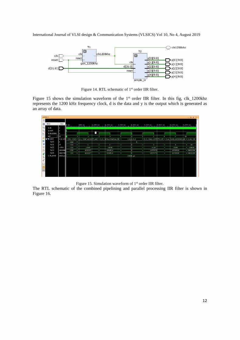
The RTL schematic of 1st order IIR filter is shown below in Figure 14.
International Journal of VLSI design & Communication Systems (VLSICS) Vol 10, No 4, August 2019
12
Figure 14. RTL schematic of 1st order IIR filter.
Figure 15 shows the simulation waveform of the 1st order IIR filter. In this fig, clk_1200khz
represents the 1200 kHz frequency clock, d is the data and y is the output which is generated as
an array of data.
Figure 15. Simulation waveform of 1st order IIR filter.
The RTL schematic of the combined pipelining and parallel processing IIR filter is shown in
Figure 16.

International Journal of VLSI design & Communication Systems (VLSICS) Vol 10, No 4, August 2019
13
Figure 16. RTL schematic of the combined pipelined and parallel processing IIR architecture.
Figure 17 shows the simulation waveform of the combined pipelined and parallel processing IIR
architecture. Here, temporal represents 3600 kHz frequency clock and clk_out2 represents the
1200 kHz frequency clock, d is the data applied and q2 is the inputs which are generated in
parallel. Yout1, Yout2 and Yout3 represents y(3k), y(3k+1) and y(3k+2) respectively. Since L=3,
three outputs are generated in a single clock cycle; outputs are generated as an array of data.
Figure 17. Simulation waveform of parallel-pipelined IIR filter.

International Journal of VLSI design & Communication Systems (VLSICS) Vol 10, No 4, August 2019
14
From the simulation results, we can see that three outputs are generated in every clock period
since the level of parallelism applied is 3. The inputs for the combined architectures for both FIR
and IIR digital filters are generated at 3600 kHz clock frequency and the outputs are generated at
1200 kHz frequency since the proposed architecture works at 1200 kHz clock frequency. From
the synthesis and utilization reports, the area in terms of look up table (LUT), power consumption
and delay of the architecture is analyzed. After analyzing, we can conclude that the combined
architectures consumes less power and has less delay for both FIR and IIR filter hence, speed is
enhanced in the proposed architecture.
9. PERFORMANCE ANALYSIS
Table1. Synthesis results of FIR and IIR filters
SL.NO. FIR 3-tap Par-pip FIR IIR 1st order Par-pip IIR
Area (in terms of
LUT)
38 out of 133800 21 out of 133800 4 out of 133800 6 out of 133800
Power 15.152W 8.053W 10.375W 5.293W
Delay 9.347ns 5.124ns 4.255ns 4.724ns
From the Table 1, we observed that at the same clock frequency i.e. 1200 kHz, the pipelined and
parallel FIR filter has less area, power consumption, and delay which mean that the speed is
increased as compared to the original 3-tap FIR filter. For the IIR filter at 1200 kHz clock
frequency, we have found that with a slight increase in area, power consumption in the filter is
reduced with less or approximately equal speed.
Table2. Comparison between the existing structure and the proposed architecture
Structures Delay(ns)
16 bit Vedic multiplier [19] 4-tap micro-programmed
sequential FIR filter
4-tap micro-programmed
Parallel FIR filter
10.56ns 14.28ns 16 bit Wallace tree multiplier [19] 4-tap micro-programmed
sequential FIR filter
4-tap micro-programmed
Parallel FIR filter
15.56ns 19.51ns
Virtex-4 (XC4VFX12) [17] Serial FIR filter Pipelined FIR filter
24.648ns 22.012ns
Virtex-5 (XC5VLX110T) [17] Serial FIR filter Pipelined FIR filter
18.696ns 15.928ns
Virtex-6 (XC6VCX75T) [17] Serial FIR filter Pipelined FIR filter
17.411ns 15.456ns
Proposed structure(Artix-7)
(xc7a200tfbg676) (speed grade -1)
Par-pip FIR
5.124ns
From Table 2, we can conclude that the proposed architecture is better than the existing structure
since the delay is less hence, speed is improved in the combined pipelining and parallel
processing architecture.
International Journal of VLSI design & Communication Systems (VLSICS) Vol 10, No 4, August 2019
15
10. CONCLUSION
In this paper, we have implemented the combined pipelining and parallel processing architecture
for both FIR and IIR filters. Synthesis and simulation are being carried out on Artix-7 series
FPGA, target device (xc7a200tfbg676) (speed grade -1) using VIVADO 2016.3. The parameters
like area, delay and power are the main focus of this research work. With two stages of pipelining
(M=2) and three levels of parallelism (L=3), FIR and IIR filters are being implemented and
results are being analyzed and compared with the non-pipelined and non-parallel original filter.
From the results, we observed that for FIR filter, in the combined architecture, with the decrease
in area, power is reduced from 15.152W to 8.053W and delay also reduces from 9.347ns to
5.124ns. Ultimately, speed increased in the proposed combined architecture. For IIR filter, with a
slight increase in the area in the combined architecture, power consumption is reduced from
10.375W to 5.293W at approximately equal speed. From Table 9.2, we can conclude that delay is
less in this proposed architecture than the existing structures.
ACKNOWLEDGEMENT
I would like to express my gratitude to Dr. Manoj Kumar, Assistant Professor in the dept. of
ECE, NIT Manipur for his endless support and valuable guidance throughout the research work.
REFERENCES
[1]. K. K. Parhi, VLSI Digital Signal Processing Systems: Design and Implementation. New York: Wiley,
1999.
[2]. S. M. Rabiul Islam, R. Sarker, S. Saha and A. F. M. Nokib Uddin, “Design of a Programmable digital
IIR filter based on FPGA” 2012 International Conference on Informatics, Electronics & Vision
(ICIEV), Dhaka, pp. 716-72, 2012.
[3]. Suresh Gawande and SnehaBhujbal “High Speed IIR Notch Filter Using Pipelined Technique”
International Journal of Advanced Research in Electrical, Electronics and Instrumentation
Engineering Vol. 6, Issue 2, February 2017.
[4]. Yu-Chi Tsao and Ken Choi“Area-Efficient VLSI Implementation for Parallel Linear- Phase FIR
Digital Filters of Odd Length Based on Fast FIR Algorithm” IEEE Transactions On Circuits And
Systems—ii: Express Briefs, Vol. 59, No. 6, June 2012.
[5]. Ravinder Kaur and Ashish Raman “Design and Implementation of High Speed IIR and FIR Filter
using Pipelining” International Journal of Computer Theory and Engineering, Vol. 3, No. 2, April
2011.
[6]. B. K. Mohanty and P. K. Meher, "A High-Performance FIR Filter Architecture for Fixed and
Reconfigurable Applications," IEEE Transactions on Very Large Scale Integration (VLSI) Systems,
vol. 24, no. 2, pp. 444-452, Feb. 2016.
[7]. https://en.wikipedia.org/wiki/Infinite_impulse_responsepage was last edited on 17 January 2019, at
20:29 (UTC).

International Journal of VLSI design & Communication Systems (VLSICS) Vol 10, No 4, August 2019
16
[8]. Aarti Sharma and Sanjay Kumar “VLSI Implementation of Pipelined FIR Filter” International Journal
of Innovative Research In Electrical, Electronics, InstrumentationAnd Control Engineering Vol. 1,
Issue 5, August 2013.
[9]. S. Khorbotly, J. E. Carletta and R. J. Veillette, “A methodology for implementing pipelined fixed-
point infinite impulse response filters,” 41st Southeastern Symposium on System Theory, Tullahoma,
TN, 2009, pp. 280-284, 2009.
[10]. Keshab K. Parhi and David G. Messerschmitt, “Pipeline Interleaving and Parallelism in Recursive
Digital Filters-Part I: Pipelining Using Scattered Look-Ahead and Decomposition” IEEE Transactions
on Acoustics, Speech, and Signal Processing, Vol. 31. No. 7, July 1989.
[11]. David A. Parker and Keshab K. Parhi, “Low-Area/Power Parallel FIR Digital Filter
Implementations,” Journal of VLSI Signal Processing 17, 75–92 (1997).
[12]. Shaila Khan and Uma Sharma, “Implementation of Low Power Area Efficient Parallel FIR Digital
Filter Structures of Odd Length Based on Common Sub expression Algorithm” International Journal
of Advanced Research in Electronics and Communication Engineering (IJARECE) Volume 5, Issue
1, January 2016.
[13]. S. Balasubramaniam and R. Bharathi, “Performance Analysis of Parallel FIR Digital Filter using
VHDL” International Journal of Computer Applications Volume 39– No.9, February 2012.
[14]. Keshab K. Parhi and David G. Messerschmitt, “Pipeline Interleaving and Parallelism in Recursive
Digital Filters-Part II: Pipelined Incremental Block Filtering” IEEE Transactions on Acoustics,
Speech, and Signal Processing. Vol 37. No.7. July1989.
[15]. KanuPriya and Rajesh Mehra “Area Efficient Design of Fir Filter using Symmetric Structure”
International Journal of Advanced Research in Computer and Communication Engineering Vol. 1,
Issue 10, December 2012.
[16]. L KholeePhimu and Manojkumar“VLSI Implementation of Area Efficient 2-parallel FIR Digital
Filter” International Journal of VLSI design & Communication Systems (VLSICS) Vol.7, No.5/6,
December 2016.
[17]. Saranya R, Pradeep C, Neena Baby and R Radhakrishnan “FPGA Synthesis of Reconfigurable
Modules for FIR Filter” International Journal of Reconfigurable and Embedded Systems (IJRES) Vol.
4, No. 2, pp. 63-70, 2015.
[18]. Mahesh Kadam, KishorSawarkar and SudhakarMande “Comparative Analysis and Efficient VLSI
Implementation of FIR Filter” International Journal of Advanced Research in Electrical, Electronics
and Instrumentation Engineering, Vol. 3, Issue 7, July 2014.
[19]. TamliDhanrajSawarkar, Prof.LokeshChawle and Prof. N.G. Narole, “Implementation of 4-Tap
Sequential and Parallel Micro-programmed Based Digital FIR Filter Architecture using VHDL”
International Journal of Innovative Research in Computer and Communication Engineering Vol. 4,
Issue 4, April 2016.
[20]. G. Deepak, P. K. Meher and A. Sluzek, "Performance Characteristics of Parallel and Pipelined
Implementation of FIR Filters in FPGA Platform," 2007 International Symposium on Signals,
Circuits and Systems, Iasi, 2007, pp. 1-4.
[21]. Manoj Kumar, “Design of IIR systolic array architecture by using linear mapping technique”,
International Journal of Computer Applications, vol.182, no.39, pp.14-19, 2019.


![Efficacy of gutta-percha solvents used in endodontic ...revodonto.bvsalud.org/pdf/rsbo/v10n4/a09v10n4.pdf · endodontic treatment failure [9]. The clinical diagnosis of the pulp and](https://static.fdocuments.us/doc/165x107/5ed5a14f1b7fdd786a1b5e23/efficacy-of-gutta-percha-solvents-used-in-endodontic-endodontic-treatment-failure.jpg)