DCP02x 2-W, Isolated, Unregulated DC/DC Converter … · OSC 800 kHz SYNC +V S Divide-by-2 Reset...
28
OSC 800 kHz SYNC +V S Divide- by-2 Reset Watchdog Startup PSU Thermal Shutdown Power Stage +V OUT ±V OUT ±V S Power Controller OSC 800 kHz SYNC +V S Divide- by-2 Reset Watchdog Startup PSU Thermal Shutdown Power Stage +V OUT COM ±V S Power Controller ±V OUT Product Folder Sample & Buy Technical Documents Tools & Software Support & Community DCP020503, DCP020505, DCP020507, DCP020509, DCP020515D, DCP021205 DCP021212, DCP021212D, DCP021515, DCP022405, DCP022405D, DCP022415D SBVS011L – MARCH 2000 – REVISED MAY 2015 DCP02x 2-W, Isolated, Unregulated DC/DC Converter Modules 1 Features 3 Description The DCP02 series is a family of 2-W, isolated, 1• 1-kV Isolation (Operational) unregulated DC/DC converter modules. Requiring a • Device-to-Device Synchronization minimum of external components and including on- • EN55022 Class B EMC Performance chip device protection, the DCP02 series of devices provide extra features such as output disable and • UL1950 Recognized Component synchronization of switching frequencies. • 7-Pin PDIP and 12-Pin SOP Packages This combination of features and small size makes the DCP02 series of devices suitable for a wide range 2 Applications of applications, and is an easy-to-use solution in • Signal Path Isolation applications requiring signal path isolation. • Ground Loop Elimination WARNING: This product has operational isolation • Data Acquisition and is intended for signal isolation only. It should not • Industrial Control and Instrumentation be used as a part of a safety isolation circuit requiring reinforced isolation. See definitions in the Feature • Test Equipment Description section. Device Information (1) PART NUMBER PACKAGE BODY SIZE (NOM) PDIP (7) 19.18 mm × 10.60 mm DCP02xxxx SOP (12) 17.90 mm × 10.33 mm (1) For all available packages, see the orderable addendum at the end of the data sheet. . . Single Output Block Diagram Dual Output Block Diagram . . . . 1 An IMPORTANT NOTICE at the end of this data sheet addresses availability, warranty, changes, use in safety-critical applications, intellectual property matters and other important disclaimers. PRODUCTION DATA.
Transcript of DCP02x 2-W, Isolated, Unregulated DC/DC Converter … · OSC 800 kHz SYNC +V S Divide-by-2 Reset...

OSC800 kHz
SYNC
+VS
Divide-by-2
Reset
WatchdogStartup
PSU Thermal
Shutdown
Power Stage
+VOUT
±VOUT
±VS
Power Controller
OSC800 kHz
SYNC
+VS
Divide-by-2
Reset
WatchdogStartup
PSU Thermal
Shutdown
Power Stage
+VOUT
COM
±VS
Power Controller
±VOUT
Product
Folder
Sample &Buy
Technical
Documents
Tools &
Software
Support &Community
DCP020503, DCP020505, DCP020507, DCP020509, DCP020515D, DCP021205DCP021212, DCP021212D, DCP021515, DCP022405, DCP022405D, DCP022415D
SBVS011L –MARCH 2000–REVISED MAY 2015
DCP02x 2-W, Isolated, Unregulated DC/DC Converter Modules1 Features 3 Description
The DCP02 series is a family of 2-W, isolated,1• 1-kV Isolation (Operational)
unregulated DC/DC converter modules. Requiring a• Device-to-Device Synchronization minimum of external components and including on-• EN55022 Class B EMC Performance chip device protection, the DCP02 series of devices
provide extra features such as output disable and• UL1950 Recognized Componentsynchronization of switching frequencies.• 7-Pin PDIP and 12-Pin SOP PackagesThis combination of features and small size makesthe DCP02 series of devices suitable for a wide range2 Applicationsof applications, and is an easy-to-use solution in• Signal Path Isolation applications requiring signal path isolation.
• Ground Loop EliminationWARNING: This product has operational isolation• Data Acquisition and is intended for signal isolation only. It should not
• Industrial Control and Instrumentation be used as a part of a safety isolation circuit requiringreinforced isolation. See definitions in the Feature• Test EquipmentDescription section.
Device Information(1)
PART NUMBER PACKAGE BODY SIZE (NOM)PDIP (7) 19.18 mm × 10.60 mm
DCP02xxxxSOP (12) 17.90 mm × 10.33 mm
(1) For all available packages, see the orderable addendum atthe end of the data sheet.
.
.
Single Output Block Diagram Dual Output Block Diagram
. .
. .
1
An IMPORTANT NOTICE at the end of this data sheet addresses availability, warranty, changes, use in safety-critical applications,intellectual property matters and other important disclaimers. PRODUCTION DATA.

DCP020503, DCP020505, DCP020507, DCP020509, DCP020515D, DCP021205DCP021212, DCP021212D, DCP021515, DCP022405, DCP022405D, DCP022415DSBVS011L –MARCH 2000–REVISED MAY 2015 www.ti.com
Table of Contents8.4 Device Functional Modes........................................ 111 Features .................................................................. 1
9 Application and Implementation ........................ 132 Applications ........................................................... 19.1 Application Information............................................ 133 Description ............................................................. 19.2 Typical Application ................................................. 134 Revision History..................................................... 2
10 Power Supply Recommendations ..................... 165 Device Comparison Table ..................................... 311 Layout................................................................... 176 Pin Configuration and Functions ......................... 4
11.1 Layout Guidelines ................................................. 177 Specifications......................................................... 511.2 Layout Example .................................................... 177.1 Absolute Maximum Ratings ...................................... 5
12 Device and Documentation Support ................. 197.2 ESD Ratings ............................................................ 512.1 Device Support .................................................... 197.3 Recommended Operating Conditions....................... 512.2 Documentation Support ....................................... 197.4 Thermal Information .................................................. 512.3 Community Resources.......................................... 197.5 Electrical Characteristics........................................... 612.4 Related Links ........................................................ 207.6 Switching Characteristics .......................................... 612.5 Trademarks ........................................................... 207.7 Typical Characteristics .............................................. 712.6 Electrostatic Discharge Caution............................ 208 Detailed Description .............................................. 812.7 Glossary ................................................................ 208.1 Overview ................................................................... 8
13 Mechanical, Packaging, and Orderable8.2 Functional Block Diagrams ....................................... 8Information ........................................................... 208.3 Feature Description................................................... 9
4 Revision History
Changes from Revision K (February 2008) to Revision L Page
• Updated Features .................................................................................................................................................................. 1• Added ESD Ratings table, Feature Description section, Device Functional Modes section, Application and
Implementation section, Power Supply Recommendations section, Layout section, Device and DocumentationSupport section, and Mechanical, Packaging, and Orderable Information section................................................................ 1
• Added Dual Output Block Diagram......................................................................................................................................... 1• Renamed pin "0V" to "COM" (output side common pin) in table............................................................................................ 4• Renamed pin "VS" to "+VS" (input voltage pin) in table .......................................................................................................... 4• Renamed pin "0V" to "–VS" (input side common pin) in table ................................................................................................ 4• Added Recommended Operating Conditions table ................................................................................................................ 5• Added Thermal Information table ........................................................................................................................................... 5• Added information to the ISOLATION section of the Electrical Characteristics table ........................................................... 6• Added Isolation section to the Feature Description section ................................................................................................... 9• Added a typical application design to the Application Information section........................................................................... 13
2 Submit Documentation Feedback Copyright © 2000–2015, Texas Instruments Incorporated
Product Folder Links: DCP020503 DCP020505 DCP020507 DCP020509 DCP020515D DCP021205 DCP021212DCP021212D DCP021515 DCP022405 DCP022405D DCP022415D

DCP020503, DCP020505, DCP020507, DCP020509, DCP020515D, DCP021205DCP021212, DCP021212D, DCP021515, DCP022405, DCP022405D, DCP022415D
www.ti.com SBVS011L –MARCH 2000–REVISED MAY 2015
5 Device Comparison Table
OUTPUT DEVICE LOAD NO LOAD BARRIERINPUT EFFICIENCYVOLTAGE OUTPUT REGULATION CURRENT CAPACITANCEVOLTAGE (%)DEVICE VNOM @ VS (TYP)(V) CURRENT 10% TO 100% IQ (mA) CISO (pF)VS (V) 100% LOADNUMBER 75% LOAD (mA) (1) LOAD (2) 0% LOAD VISO = 750Vrms
MIN TYP MAX MIN TYP MAX MAX TYP MAX TYP TYP TYP
DCP020503P 3.13 3.3 3.46 600 19 30 18 74 26DCP020503U
DCP020505P 4.75 5 5.25 400 14 20 18 80 22DCP020505U
DCP020507P 4.5 5 5.5 6.65 7 7.35 285 14 25 20 81 30DCP020507U
DCP020509P 8.55 9 9.45 222 12 20 23 82 31DCP020509U
DCP020515DP ±14.25 ±15 ±15.75 133 (3) 11 20 27 85 24DCP020515DU
DCP021205P 4.75 5 5.25 400 7 15 14 83 33DCP021205U
DCP021212P 10.8 12 13.2 11.4 12 12.6 166 7 20 15 87 47DCP021212U
DCP021212DP ±11.4 ±12 ±12.6 166 (3) 6 20 16 88 35DCP021212DU
DCP021515P 13.5 15 16.5 14.25 15 15.75 133 6 20 15 88 42DCP021515U
DCP022405P 4.75 5 5.25 400 6 15 13 81 33DCP022405U
DCP022405DP 21.6 24 26.4 ±4.75 ±5 ±5.25 400 (3) 6 15 12 80 22DCP022405DU
DCP022415DP ±14.25 ±15 ±15.75 133 (3) 6 25 16 79 44DCP022415DU
(1) POUT(max) = 2 W(2) Load regulation = (VOUT at 10% load – VOUT at 100%)/VOUT at 75% load(3) IOUT1 + IOUT2
Copyright © 2000–2015, Texas Instruments Incorporated Submit Documentation Feedback 3
Product Folder Links: DCP020503 DCP020505 DCP020507 DCP020509 DCP020515D DCP021205 DCP021212DCP021212D DCP021515 DCP022405 DCP022405D DCP022415D

DCP02
1
2
3
12
13
14
28
27
26
17
16
15
+VS
–VS
–VS
–VOUT
+VOUT
NC
SYNC
NC
NC
NC
NC
NC
DCP02
1
2
3
12
13
14
28
27
26
17
16
15
+VS
–VS
–VS
COM
+VOUT
-VOUT
SYNC
NC
NC
NC
NC
NC
DCP02
1
2
5
6
7
14
8
+VS
–VS
–VOUT
+VOUT
NC
SYNC
NC
DCP02
1
2
5
6
7
14
8
+VS
–VS
COM
+VOUT
-VOUT
SYNC
NC
DCP020503, DCP020505, DCP020507, DCP020509, DCP020515D, DCP021205DCP021212, DCP021212D, DCP021515, DCP022405, DCP022405D, DCP022415DSBVS011L –MARCH 2000–REVISED MAY 2015 www.ti.com
6 Pin Configuration and Functions
NVA Package NVA Package7-Pin PDIP (Single Output) 7-Pin PDIP (Dual Output)
(Top View) (Top View)
DVB PACKAGE DVB Package12-Pin SOP (Single Output) 12-Pin SOP (Dual Output)
(Top View) (Top View)
Pin FunctionsNUMBER
PIN I/O (1) DESCRIPTIONDVB DVB NVA NVANAME(DUAL) (SINGLE) (DUAL) (SINGLE)
COM 12 — 5 — O Output side common14
1515 7
16 16NC 8 — No connection
17 1726 26 827 27
Synchronization Pin - Synchronize multiple devices by connectingSYNC 28 28 14 14 I their SYNC pins together. Pulling this pin low disables the internal
oscillator.+VOUT 13 13 6 6 O Positive output voltage–VOUT 14 12 7 5 O Negative output voltage+VS 1 1 1 1 I Input voltage
2 2–VS 2 2 I Input side common
3 3
(1) I = Input, O = Output
4 Submit Documentation Feedback Copyright © 2000–2015, Texas Instruments Incorporated
Product Folder Links: DCP020503 DCP020505 DCP020507 DCP020509 DCP020515D DCP021205 DCP021212DCP021212D DCP021515 DCP022405 DCP022405D DCP022415D

DCP020503, DCP020505, DCP020507, DCP020509, DCP020515D, DCP021205DCP021212, DCP021212D, DCP021515, DCP022405, DCP022405D, DCP022415D
www.ti.com SBVS011L –MARCH 2000–REVISED MAY 2015
7 Specifications
7.1 Absolute Maximum Ratingsover operating free-air temperature range (unless otherwise noted) (1)
MIN MAX UNIT5-V input devices 712-V input devices 15
Input voltage V15-V input devices 1824-V input devices 29
Storage temperature, Tstg –60 125 °C
(1) Stresses beyond those listed under Absolute Maximum Ratings may cause permanent damage to the device. These are stress ratingsonly, which do not imply functional operation of the device at these or any other conditions beyond those indicated under RecommendedOperating Conditions. Exposure to absolute-maximum-rated conditions for extended periods may affect device reliability.
7.2 ESD RatingsVALUE UNIT
Human-body model (HBM), per ANSI/ESDA/JEDEC JS-001 (1) ±1000V(ESD) Electrostatic discharge VCharged-device model (CDM), per JEDEC specification JESD22- ±250C101 (2)
(1) JEDEC document JEP155 states that 500-V HBM allows safe manufacturing with a standard ESD control process.(2) JEDEC document JEP157 states that 250-V CDM allows safe manufacturing with a standard ESD control process.
7.3 Recommended Operating Conditionsover operating free-air temperature range (unless otherwise noted)
MIN NOM MAX UNIT5-V input devices 4.5 5 5.512-V input devices 10.8 12 13.2
Input Voltage V15-V input devices 13.5 15 16.524-V input devices 21.6 24 26.4
Operating temperature –40 85 °C
7.4 Thermal InformationDCP020x DCP020x
THERMAL METRIC (1) NVA (PDIP) DVB (SOP) UNIT7 PINS 12 PINS
RθJA Junction-to-ambient thermal resistance 61 61RθJC(top) Junction-to-case (top) thermal resistance 19 19RθJB Junction-to-board thermal resistance 24 24
°C/WψJT Junction-to-top characterization parameter 7 7ψJB Junction-to-board characterization parameter 24 24RθJC(bot) Junction-to-case (bottom) thermal resistance N/A N/A
(1) For more information about traditional and new thermal metrics, see the Semiconductor and IC Package Thermal Metrics applicationreport, SPRA953.
Copyright © 2000–2015, Texas Instruments Incorporated Submit Documentation Feedback 5
Product Folder Links: DCP020503 DCP020505 DCP020507 DCP020509 DCP020515D DCP021205 DCP021212DCP021212D DCP021515 DCP022405 DCP022405D DCP022415D

DCP020503, DCP020505, DCP020507, DCP020509, DCP020515D, DCP021205DCP021212, DCP021212D, DCP021515, DCP022405, DCP022405D, DCP022415DSBVS011L –MARCH 2000–REVISED MAY 2015 www.ti.com
7.5 Electrical Characteristicsover operating free-air temperature range (unless otherwise noted)
PARAMETER TEST CONDITIONS MIN TYP MAX UNITOUTPUTPOUT Output power ILOAD = 100% (full load) 2 WVRIPPLE Output voltage ripple COUT = 1 μF, ILOAD = 50% 20 mVPP
–40°C ≤ TA ≤ 25°C 0.046 %/°CVoltage vs. Temperature
25°C ≤ TA ≤ 85°C 0.016 %/°CINPUTVS Input voltage range –10% 10%ISOLATION
Voltage 1 kVrms1-second flash test dV/dt 500 V/s
Leakage Current 30 nAVISO IsolationContinuous working DC 60 VDCvoltage across isolation
AC 42.5 VACbarrierLINE REGULATION
IOUT ≥ 10% load current and constant, 1% 15%VS (min) to VS (typ)Output voltage
IOUT ≥ 10% load current and constant, 1% 15%VS (typ) to VS (max)RELIABILITY
Demonstrated TA = 55°C 75 FITSTHERMAL SHUTDOWN
Die temperature atTSD 150 °CshutdownISD Shutdown current 3 mA
7.6 Switching Characteristicsover operating free-air temperature range (unless otherwise noted)
PARAMETER TEST CONDITIONS MIN TYP MAX UNITfOSC Oscillator frequency fSW = fOSC/2 800 kHzVIL Low-level input voltage, SYNC 0 0.4 VISYNC Input current, SYNC VSYNC = 2 V 75 µAtDISABLE Disable time 2 µsCSYNC Capacitance loading on SYNC pin (1) External 3 pF
(1) The application report External Synchronization of the DCP01/02 Series of DC/DC Converters(SBAA035) describes this configuration.
6 Submit Documentation Feedback Copyright © 2000–2015, Texas Instruments Incorporated
Product Folder Links: DCP020503 DCP020505 DCP020507 DCP020509 DCP020515D DCP021205 DCP021212DCP021212D DCP021515 DCP022405 DCP022405D DCP022415D

Load (%)
100
80
60
40
20
0250 50 75 100
Effi
cien
cy (
%)
DCP021212DPDCP021205P
Load Current (mA)
450
400
300
200
100
01000 200 300 400
Out
put A
C R
ippl
e (m
VP
-P)
350
250
150
50
COUT = 1 µFCOUT = 0.1 µF
Load (%)
5.4
5.3
5.2
5.1
5.0
4.9200 40 60 10080
Out
put V
olta
ge (
V)
Temperature (°C)
2.5
2.0
1.5
1.0
0.5
0±25±50 25 50 10075
Out
put P
ower
(W
)
0
Frequency (MHz)
60
50
30
10
0
±2010.15 10 30
Pea
k E
mis
sion
Lev
el (
dB/µ
A)
40
20
±10
Series 1Series 2Series 3
Temperature (°C)
5.04
5.02
5.00
4.98
4.96
4.94
4.92
4.90±20±40 200 6040 10080
Out
put V
olta
ge (
V)
DCP020503, DCP020505, DCP020507, DCP020509, DCP020515D, DCP021205DCP021212, DCP021212D, DCP021515, DCP022405, DCP022405D, DCP022415D
www.ti.com SBVS011L –MARCH 2000–REVISED MAY 2015
7.7 Typical CharacteristicsTA = 25°C, unless otherwise noted.
DCP020505P ILOAD = 400 mA DCP020505P 75% Load Current
Figure 1. Conducted Emmisions vs. Frequency Figure 2. Output Voltage vs. Temperature
DCP021205P DCP021205P ILOAD = 400 mA
Figure 3. Output Voltage vs. Output Current Figure 4. Output Power vs. Temperature
DCP020505P (20 MHzbandwidth)
Figure 5. Efficiency vs. Percent Load CurrentFigure 6. Output AC Ripple vs. Load Current
Copyright © 2000–2015, Texas Instruments Incorporated Submit Documentation Feedback 7
Product Folder Links: DCP020503 DCP020505 DCP020507 DCP020509 DCP020515D DCP021205 DCP021212DCP021212D DCP021515 DCP022405 DCP022405D DCP022415D

Oscillator
800 kHzSYNC
+VS
Divide-by-2
Reset
Watchdog
Startup
PSU Thermal
Shutdown
Power
Stage
+VOUT
–VOUT
–VS
Power Controller
COM
Oscillator
800 kHzSYNC
+VS
Divide-by-2
Reset
Watchdog
Startup
PSU Thermal
Shutdown
Power
Stage
+VOUT
–VOUT
–VS
Power Controller
DCP020503, DCP020505, DCP020507, DCP020509, DCP020515D, DCP021205DCP021212, DCP021212D, DCP021515, DCP022405, DCP022405D, DCP022415DSBVS011L –MARCH 2000–REVISED MAY 2015 www.ti.com
8 Detailed Description
8.1 OverviewThe DCP02 offers up to 2 W of isolated, unregulated output power from a 5-V, 12-V, 15-V, or 24-V input sourcewith a typical efficiency of up to 89%. This efficiency is achieved through highly integrated packaging technologyand the implementation of a custom power stage and control device. The DCP02 devices are specified foroperational isolation only. The circuit design uses an advanced BiCMOS/DMOS process.
8.2 Functional Block Diagrams
Figure 7. Single Output Device
Figure 8. Dual Output Device
8 Submit Documentation Feedback Copyright © 2000–2015, Texas Instruments Incorporated
Product Folder Links: DCP020503 DCP020505 DCP020507 DCP020509 DCP020515D DCP021205 DCP021212DCP021212D DCP021515 DCP022405 DCP022405D DCP022415D

DCP020503, DCP020505, DCP020507, DCP020509, DCP020515D, DCP021205DCP021212, DCP021212D, DCP021515, DCP022405, DCP022405D, DCP022415D
www.ti.com SBVS011L –MARCH 2000–REVISED MAY 2015
8.3 Feature Description
8.3.1 IsolationUnderwriters Laboratories, UL™ defines several classes of isolation that are used in modern power supplies.
Safety extra low voltage (SELV) is defined by UL (UL1950 E199929) as a secondary circuit which is sodesignated and protected that under normal and single fault conditions the voltage between any two accessibleparts, or between an accessible part and the equipment earthing terminal for operational isolation does notexceed steady state 42 V peak or 60 VDC for more than 1 second.
8.3.1.1 Operation or Functional IsolationOperational or functional isolation is defined by the use of a high-potential (hipot) test only. Typically, thisisolation is defined as the use of insulated wire in the construction of the transformer as the primary isolationbarrier. The hipot one-second duration test (dielectric voltage, withstand test) is a production test used to verifythat the isolation barrier is functioning. Products with operational isolation should never be used as an element ina safety-isolation system.
8.3.1.2 Basic or Enhanced IsolationBasic or enhanced isolation is defined by specified creepage and clearance limits between the primary andsecondary circuits of the power supply. Basic isolation is the use of an isolation barrier in addition to the insulatedwire in the construction of the transformer. Input and output circuits must also be physically separated byspecified distances.
8.3.1.3 Continuous VoltageFor a device that has no specific safety agency approvals (operational isolation), the continuous voltage that canbe applied across the part in normal operation is less than 42.4 VRMS, or 60 VDC. Ensure that both input andoutput voltages maintain normal SELV limits. The isolation test voltage represents a measure of immunity totransient voltages.
WARNINGDo not use the device as an element of a safety isolation system when SELV isexceeded
If the device is expected to function correctly with more than 42.4 VRMS or 60 VDC applied continuously across theisolation barrier, then the circuitry on both sides of the barrier must be regarded as operating at an unsafevoltage, and further isolation or insulation systems must form a barrier between these circuits and any user-accessible circuitry according to safety standard requirements.
8.3.1.4 Isolation VoltageHipot test, flash-tested, withstand voltage, proof voltage, dielectric withstand voltage, and isolation test voltageare all terms that relate to the same thing: a test voltage applied for a specified time across a componentdesigned to provide electrical isolation to verify the integrity of that isolation. TI’s DCP02 series of dc-dcconverters are all 100% production tested at 1.0 kVAC for one second.
8.3.1.5 Repeated High-Voltage Isolation TestingRepeated high-voltage isolation testing of a barrier component can degrade the isolation capability, depending onmaterials, construction, and environment. The DCP02 series of dc-dc converters have toroidal, enameled, wireisolation transformers with no additional insulation between the primary and secondary windings. While a devicecan be expected to withstand several times the stated test voltage, the isolation capability depends on the wireinsulation. Any material, including this enamel (typically polyurethane), is susceptible to eventual chemicaldegradation when subject to very-high applied voltages. Therefore, strictly limit the number of high-voltage testsand repeated high-voltage isolation testing. However, if it is absolutely required, reduce the voltage by 20% fromspecified test voltage with a duration limit of one second per test.
Copyright © 2000–2015, Texas Instruments Incorporated Submit Documentation Feedback 9
Product Folder Links: DCP020503 DCP020505 DCP020507 DCP020509 DCP020515D DCP021205 DCP021212DCP021212D DCP021515 DCP022405 DCP022405D DCP022415D
DCP020503, DCP020505, DCP020507, DCP020509, DCP020515D, DCP021205DCP021212, DCP021212D, DCP021515, DCP022405, DCP022405D, DCP022415DSBVS011L –MARCH 2000–REVISED MAY 2015 www.ti.com
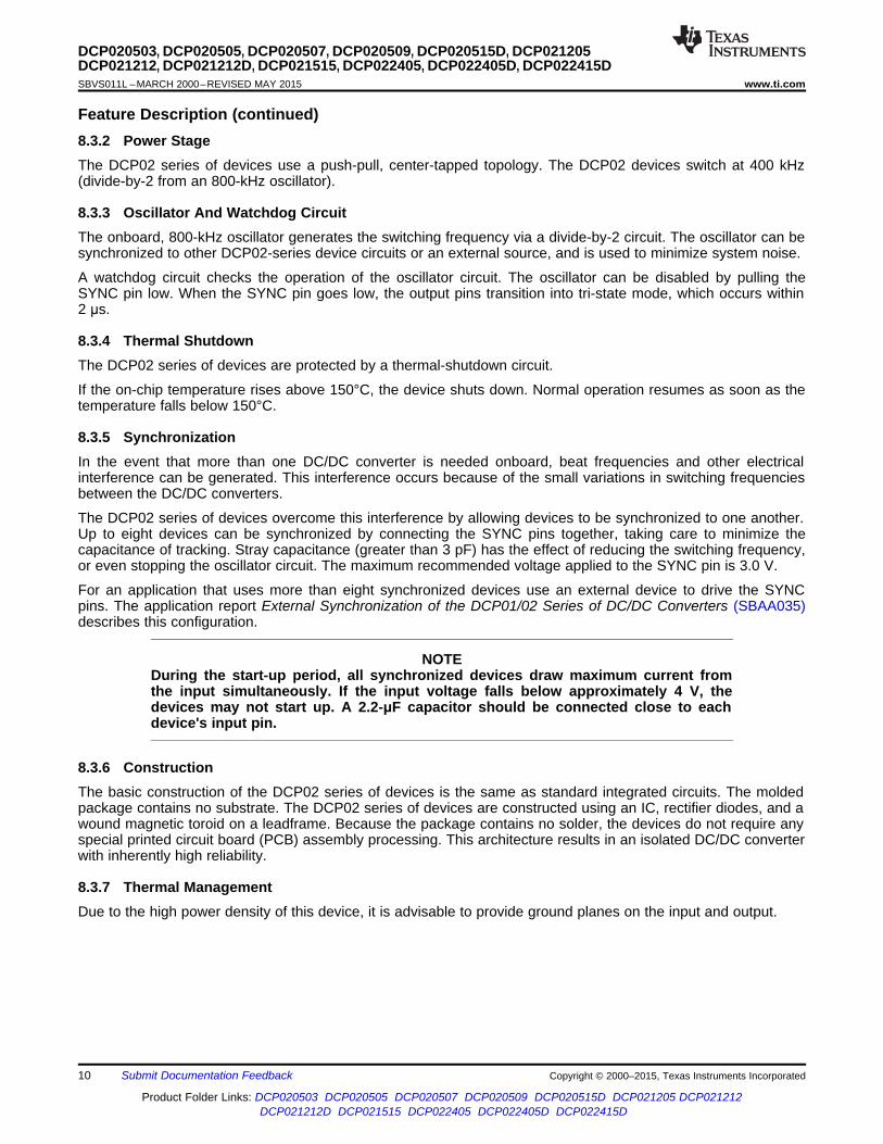
Feature Description (continued)8.3.2 Power StageThe DCP02 series of devices use a push-pull, center-tapped topology. The DCP02 devices switch at 400 kHz(divide-by-2 from an 800-kHz oscillator).
8.3.3 Oscillator And Watchdog CircuitThe onboard, 800-kHz oscillator generates the switching frequency via a divide-by-2 circuit. The oscillator can besynchronized to other DCP02-series device circuits or an external source, and is used to minimize system noise.
A watchdog circuit checks the operation of the oscillator circuit. The oscillator can be disabled by pulling theSYNC pin low. When the SYNC pin goes low, the output pins transition into tri-state mode, which occurs within2 μs.
8.3.4 Thermal ShutdownThe DCP02 series of devices are protected by a thermal-shutdown circuit.
If the on-chip temperature rises above 150°C, the device shuts down. Normal operation resumes as soon as thetemperature falls below 150°C.
8.3.5 SynchronizationIn the event that more than one DC/DC converter is needed onboard, beat frequencies and other electricalinterference can be generated. This interference occurs because of the small variations in switching frequenciesbetween the DC/DC converters.
The DCP02 series of devices overcome this interference by allowing devices to be synchronized to one another.Up to eight devices can be synchronized by connecting the SYNC pins together, taking care to minimize thecapacitance of tracking. Stray capacitance (greater than 3 pF) has the effect of reducing the switching frequency,or even stopping the oscillator circuit. The maximum recommended voltage applied to the SYNC pin is 3.0 V.
For an application that uses more than eight synchronized devices use an external device to drive the SYNCpins. The application report External Synchronization of the DCP01/02 Series of DC/DC Converters (SBAA035)describes this configuration.
NOTEDuring the start-up period, all synchronized devices draw maximum current fromthe input simultaneously. If the input voltage falls below approximately 4 V, thedevices may not start up. A 2.2-μF capacitor should be connected close to eachdevice's input pin.
8.3.6 ConstructionThe basic construction of the DCP02 series of devices is the same as standard integrated circuits. The moldedpackage contains no substrate. The DCP02 series of devices are constructed using an IC, rectifier diodes, and awound magnetic toroid on a leadframe. Because the package contains no solder, the devices do not require anyspecial printed circuit board (PCB) assembly processing. This architecture results in an isolated DC/DC converterwith inherently high reliability.
8.3.7 Thermal ManagementDue to the high power density of this device, it is advisable to provide ground planes on the input and output.
10 Submit Documentation Feedback Copyright © 2000–2015, Texas Instruments Incorporated
Product Folder Links: DCP020503 DCP020505 DCP020507 DCP020509 DCP020515D DCP021205 DCP021212DCP021212D DCP021515 DCP022405 DCP022405D DCP022415D

VIN
COUT
1.0 µFDCP 02
+VS
–VS
+VOUT
COM
CIN
–VOUT
COUT
1.0 µF
+VOUT
–VOUT
VIN
COUT
1.0 µFDCP 02
+VS
SYNC
–VS
+VOUT1
–VOUT1
COUT
1.0 µFDCP 02
VS
SYNC
–VS
+VOUT2
–VOUT2
CIN
CIN
VOUT1
+
VOUT2
DCP020503, DCP020505, DCP020507, DCP020509, DCP020515D, DCP021205DCP021212, DCP021212D, DCP021515, DCP022405, DCP022405D, DCP022415D
www.ti.com SBVS011L –MARCH 2000–REVISED MAY 2015
8.4 Device Functional Modes
8.4.1 Disable/Enable (SYNC pin)Any of the DCP02 series devices can be disabled or enabled by driving the SYNC pin using an open drainCMOS gate. If the SYNC pin is pulled low, the DCP02 becomes disabled. The disable time depends upon theexternal loading. The internal disable function is implemented in 2 μs. Removal of the pull down causes theDCP02 to be enabled.
Capacitive loading on the SYNC pin should be minimized (≤ 3 pF) in order to prevent a reduction in the oscillatorfrequency. The application report External Synchronization of the DCP01/02 Series of DC/DC Converters(SBAA035) describes disable/enable control circuitry.
8.4.2 Decoupling
8.4.2.1 Ripple ReductionThe high switching frequency of 400 kHz allows simple filtering. To reduce ripple, it is recommended that aminimum of 1-μF capacitor be used on the VOUT pin. For dual output devices, decouple both of the outputs to theCOM pin. A 2.2-μF capacitor on the input is also recommended.
8.4.2.2 Connecting the DCP02 in SeriesMultiple DCP02 isolated 2W DC/DC converters can be connected in series to provide non-standard voltage rails.This configuration is possible by using the floating outputs provided by the galvanic isolation of the DCP02.
Connect the +VOUT from one DCP02 to the –VOUT of another (see Figure 9). If the SYNC pins are tied together,the self-synchronization feature of the DCP02 prevents beat frequencies on the voltage rails. The SYNC featureof the DCP02 allows easy series connection without external filtering, thus minimizing cost.
The outputs of a dual-output DCP02 can also be connected in series to provide two times the magnitude of VOUT,as shown in Figure 10. For example, connect a dual-output, 15-V, DCP022415D device to provide a 30-V rail.
All 5-V, 12-V, and 15-V input voltage designs require a2.2-μF, low-ESR ceramic input capacitor, while 24-V inputapplications require only 0.47 μF of input capacitance.
Figure 9. Multiple DCP02 Devices Connected in Series
Figure 10. Dual Output Devices Connected in Series
Copyright © 2000–2015, Texas Instruments Incorporated Submit Documentation Feedback 11
Product Folder Links: DCP020503 DCP020505 DCP020507 DCP020509 DCP020515D DCP021205 DCP021212DCP021212D DCP021515 DCP022405 DCP022405D DCP022415D

VIN
COUT
1.0 µF
DCP 02
+VS
–VS
+VOUT1
–VOUT1
CIN
COUT
1.0 µF
2 × Power Out
GND
DCP 02
+VS
–VS
+VOUT2
–VOUT2
SYNC
SYNCCIN
DCP020503, DCP020505, DCP020507, DCP020509, DCP020515D, DCP021205DCP021212, DCP021212D, DCP021515, DCP022405, DCP022405D, DCP022415DSBVS011L –MARCH 2000–REVISED MAY 2015 www.ti.com
8.4.2.3 Connecting the DCP02 in ParallelIf the output power from one DCP02 is not sufficient, it is possible to parallel the outputs of multiple DCP02s, asshown in Figure 11, ( applies to single output devices only). The SYNC feature allows easy synchronization toprevent power-rail beat frequencies at no additional filtering cost.
All 5-V, 12-V, and 15-V input voltage designs require a 2.2-μF, low-ESR, ceramic input capacitor, while 24-Vinput applications require only 0.47 μF of input capacitance.
Figure 11. Multiple DCP02 Devices Connected in Parallel
12 Submit Documentation Feedback Copyright © 2000–2015, Texas Instruments Incorporated
Product Folder Links: DCP020503 DCP020505 DCP020507 DCP020509 DCP020515D DCP021205 DCP021212DCP021212D DCP021515 DCP022405 DCP022405D DCP022415D

20
30
40
50
60
70
80
90
100
0 20 40 60 80 100
Effi
cien
cy (
%)
Load Current (%) C001
4.5
4.7
4.9
5.1
5.3
5.5
5.7
5.9
0 20 40 60 80 100
Out
put V
olta
ge (
V)
Load Current (%) C004
VIN
COUT
1.0 µF
DCP02
+VS
–VS
+VOUT
CIN
2.2 µF
–VOUT
+VOUT
–VOUT
SYNC
DCP020503, DCP020505, DCP020507, DCP020509, DCP020515D, DCP021205DCP021212, DCP021212D, DCP021515, DCP022405, DCP022405D, DCP022415D
www.ti.com SBVS011L –MARCH 2000–REVISED MAY 2015
9 Application and Implementation
NOTEInformation in the following applications sections is not part of the TI componentspecification, and TI does not warrant its accuracy or completeness. TI’s customers areresponsible for determining suitability of components for their purposes. Customers shouldvalidate and test their design implementation to confirm system functionality.
9.1 Application Information
9.2 Typical Application
Figure 12. Typical DCP020505 Application
9.2.1 Design RequirementsFor this design example, use the parameters listed in Table 1 and follow the design procedures shown inDetailed Design Procedure section.
Table 1. Design Example ParametersPARAMETER VALUE UNIT
V(+VS) Input voltage 5 VV(+VOUT) Output voltage 5 VIOUT Output current rating 400 mAfSW Operating frequency 400 kHz
9.2.2 DCP020505 Application Curves
DCP020505 Load RegulationDCP020505 Efficiency
Figure 14. DCP020505 Load RegulationFigure 13. DCP020505 Efficiency
Copyright © 2000–2015, Texas Instruments Incorporated Submit Documentation Feedback 13
Product Folder Links: DCP020503 DCP020505 DCP020507 DCP020509 DCP020515D DCP021205 DCP021212DCP021212D DCP021515 DCP022405 DCP022405D DCP022415D

Frequency (Hz)
Cap
acito
r Im
peda
nce
( )
f0
XC
XL
0
Z
DCP020503, DCP020505, DCP020507, DCP020509, DCP020515D, DCP021205DCP021212, DCP021212D, DCP021515, DCP022405, DCP022405D, DCP022415DSBVS011L –MARCH 2000–REVISED MAY 2015 www.ti.com
9.2.3 Detailed Design Procedure
9.2.3.1 Input CapacitorFor all 5-V, 12-V, and 15-V input voltage designs, select a 2.2-μF low-ESR ceramic input capacitor to ensure agood startup performance. 24-V input applications require only 0.47-μF of input capacitance.
9.2.3.2 Output CapacitorFor any DCP02 design, select a 1.0-μF low-ESR ceramic output capacitor to reduce output ripple.
9.2.3.3 SYNC PinIn a stand-alone application, leave the SYNC pin floating.
9.2.4 PCB DesignThe copper losses (resistance and inductance) can be minimized by the use of mutual ground and power planes(tracks) where possible. If that is not possible, use wide tracks to reduce the losses. If several devices are beingpowered from a common power source, a star-connected system for the track must be deployed; devices mustnot be connected in series, as this will cascade the resistive losses. The position of the decoupling capacitors isimportant. They must be as close to the devices as possible in order to reduce losses. See the PCB Layoutsection for more details.
9.2.5 Decoupling Ceramic CapacitorsAll capacitors have losses because of internal equivalent series resistance (ESR), and to a lesser degree,equivalent series inductance (ESL). Values for ESL are not always easy to obtain. However, somemanufacturers provide graphs of frequency versus capacitor impedance. These graphs typically show thecapacitor impedance falling as frequency is increased (as shown in Figure 15). In Figure 15, XC is the reactancedue to the capacitance, XL is the reactance due to the ESL, and f0 is the resonant frequency. As the frequencyincreases, the impedance stops decreasing and begins to rise. The point of minimum impedance indicates theresonant frequency of the capacitor. This frequency is where the components of capacitance and inductancereactance are of equal magnitude. Beyond this point, the capacitor is not effective as a capacitor.
Figure 15. Capacitor Impedance vs Frequency
At f0, XC = XL; however, there is a 180° phase difference resulting in cancellation of the imaginary component.The resulting effect is that the impedance at the resonant point is the real part of the complex impedance;namely, the value of the ESR. The resonant frequency must be well above the 800-kHz switching frequency ofthe DCP and DCVs.
14 Submit Documentation Feedback Copyright © 2000–2015, Texas Instruments Incorporated
Product Folder Links: DCP020503 DCP020505 DCP020507 DCP020509 DCP020515D DCP021205 DCP021212DCP021212D DCP021515 DCP022405 DCP022405D DCP022415D

DCP020503, DCP020505, DCP020507, DCP020509, DCP020515D, DCP021205DCP021212, DCP021212D, DCP021515, DCP022405, DCP022405D, DCP022415D
www.ti.com SBVS011L –MARCH 2000–REVISED MAY 2015
The effect of the ESR is to cause a voltage drop within the capacitor. The value of this voltage drop is simply theproduct of the ESR and the transient load current, as shown in Equation 1.
VIN = VPK – (ESR × ITR)
where• VIN is the voltage at the device input• VPK is the maximum value of the voltage on the capacitor during charge• ITR is the transient load current (1)
The other factor that affects the performance is the value of the capacitance. However, for the input and the fullwave outputs (single-output voltage devices), ESR is the dominant factor.
9.2.6 Input Capacitor and the Effects of ESRIf the input decoupling capacitor is not ceramic (and has an ESR greater than 20 mΩ), then at the instant thepower transistors switch on, the voltage at the input pins falls momentarily. If the voltage falls belowapproximately 4 V, the DCP detects an undervoltage condition and switches the DCP drive circuits to the offstate. This detection is carried out as a precaution against a genuine low input voltage condition that could slowdown or even stop the internal circuits from operating correctly. A slow-down or stoppage results in the drivetransistors being turned on too long, causing saturation of the transformer and destruction of the device.
Following detection of a low input voltage condition, the device switches off the internal drive circuits until theinput voltage returns to a safe value, at which time the device tries to restart. If the input capacitor is still unableto maintain the input voltage, shutdown recurs. This process repeats until the input capacitor charges sufficientlyto start the device correctly.
Normal startup should occur in approximately 1 ms after power is applied to the device. If a considerably longerstartup duration time is encountered, it is likely that either (or both) the input supply or the capacitors are notperforming adequately.
For 5-V to 15-V input devices, a 2.2-μF, low-ESR ceramic capacitor ensures a good startup performance. For 24-V input voltage devices, 0.47 μF ceramic capacitors are recommended. Tantalum capacitors are notrecommended, since most do not have low-ESR values and will degrade performance. If tantalum capacitorsmust be used, close attention must be paid to both the ESR and voltage as derated by the vendor.
NOTEDuring the start-up period, these devices may draw maximum current from the inputsupply. If the input voltage falls below approximately 4 V, the devices may not startup. Connect a 2.2-μF ceramic capacitor close to the input pins.
9.2.7 Ripple and NoiseA good quality, low-ESR ceramic capacitor placed as close as practical across the input reduces reflected rippleand ensures a smooth startup.
A good quality, low-ESR ceramic capacitor placed as close as practical across the rectifier output terminal andoutput ground gives the best ripple and noise performance. See DC-to-DC Converter Noise Reduction(SBVA012), for more information on noise rejection.
9.2.7.1 Output Ripple Calculation ExampleThe following example shows that increasing the capacitance has a much smaller effect on the output ripplevoltage than does reducing the value of the ESR for the filter capacitor.
To calculate the output ripple for a DCP020505 device:• VOUT = 5 V• IOUT = 0.4 A• At full output power, the load resistor is 12.5Ω• Output capacitor of 1μF, ESR of 0.1Ω• Capacitor discharge time 1% of 800 kHz (ripple frequency
tDIS = 0.0125 μs
Copyright © 2000–2015, Texas Instruments Incorporated Submit Documentation Feedback 15
Product Folder Links: DCP020503 DCP020505 DCP020507 DCP020509 DCP020515D DCP021205 DCP021212DCP021212D DCP021515 DCP022405 DCP022405D DCP022415D

DCP020503, DCP020505, DCP020507, DCP020509, DCP020515D, DCP021205DCP021212, DCP021212D, DCP021515, DCP022405, DCP022405D, DCP022415DSBVS011L –MARCH 2000–REVISED MAY 2015 www.ti.com
τ = C × RLOADτ = 1 × 10-6 × 12.5 = 12.5 μsVDIS = VO(1 – EXP(–tDIS/τ))VDIS = 5 mV
By contrast, the voltage dropped because of ESR:VESR = ILOAD × ESRVESR = 40 mVRipple voltage = 45 mV
9.2.8 Dual DCP02 Output VoltageThe voltage output for dual DCP02 devices is half wave rectified; therefore, the discharge time is 1.25 μs.Repeating the above calculations using the 100% load resistance of 25 Ω (0.2 A per output), the results are:
τ = 25 μstDIS = 1.25 μsVDIS = 244 mVVESR = 20 mVRipple Voltage = 266 mV
This time, it is the capacitor discharging that contributes to the largest component of ripple. Changing the outputfilter to 10 μF, and repeating the calculations, the result is:
Ripple Voltage = 45 mV.
This value is composed of almost equal components.
The previous calculations are offered as a guideline only. Capacitor parameters usually have large tolerancesand can be susceptible to environmental conditions.
9.2.9 Optimizing PerformanceOptimum performance can only be achieved if the device is correctly supported. The very nature of a switchingconverter requires power to be instantly available when it switches on. If the converter has DMOS switchingtransistors, the fast edges will create a high current demand on the input supply. This transient load placed onthe input is supplied by the external input decoupling capacitor, thus maintaining the input voltage. Therefore, theinput supply does not see this transient (this is an analogy to high-speed digital circuits). The positioning of thecapacitor is critical and must be placed as close as possible to the input pins and connected via a low-impedancepath.
The optimum performance primarily depends on two factors:• Connection of the input and output circuits for minimal loss.• The ability of the decoupling capacitors to maintain the input and output voltages at a constant level.
10 Power Supply RecommendationsThe DCP02 is a switching power supply, and as such can place high peak current demands on the input supply.In order to avoid the supply falling momentarily during the fast switching pulses, ground and power planes shouldbe used to connect the power to the input of DCP02. If this connection is not possible, then the supplies must beconnected in a star formation with the traces made as wide as possible.
16 Submit Documentation Feedback Copyright © 2000–2015, Texas Instruments Incorporated
Product Folder Links: DCP020503 DCP020505 DCP020507 DCP020509 DCP020515D DCP021205 DCP021212DCP021212D DCP021515 DCP022405 DCP022405D DCP022415D

+VS
–VS
DCP02xxxxP
+VOUT
–VOUT
1
2
6
7
C1
C2
COM5
C4
C2-1
C4-1
C3
C5
R1
R2
14SYNC JP1VS1
0V1
+V1
COM1
– V1
+VS
–VS
DCP02xxxxP
+VOUT
–VOUT
1
2
6
7
C6
C7
COM5
C9
C7-1
C9-1
C8
C10
R3
R4
14SYNC JP2VS2
0V2
+V2
COM2
– V2
CON1
CON2
+VS
–VS
DCP02xxxxU
+VOUT
–VOUT
1
2
13
14
C11
C12
COM12
C15
C13
C14
R5
R6
28SYNC JP1VS3
0V3
+V3
COM3
– V3
JP2
CON3
CON4
27
26
NC
NC
–VS3
+VS
–VS
+VOUT
–VOUT
1
2
13
14
C16
C18
COM12
C19
C17
C20
R7
R8
28SYNCVS4
0V4
+V4
COM4
– V4
27
26
NC
NC
–VS3
DCP02xxxxU
DCP020503, DCP020505, DCP020507, DCP020509, DCP020515D, DCP021205DCP021212, DCP021212D, DCP021515, DCP022405, DCP022405D, DCP022415D
www.ti.com SBVS011L –MARCH 2000–REVISED MAY 2015
11 Layout
11.1 Layout GuidelinesDue to the high power density of these devices, provide ground planes on the input and output.
Figure 19 and Figure 17 illustrate a printed circuit board (PCB) layout for the two conventional (DCP01/02,DCV01), and two SOP surface-mount packages (DCP02U). Figure 16 shows the schematic.
Including input power and ground planes provides a low-impedance path for the input power. For the output, theCOM signal connects via a ground plane, while the connections for the positive and negative voltage outputsconduct via wide traces in order to minimize losses.
The output should be taken from the device using ground and power planes, thereby ensuring minimum losses.
The location of the decoupling capacitors in close proximity to their respective pins ensures low losses due to theeffects of stray inductance, thus improving the ripple performance. This location is of particular importance to theinput decoupling capacitor, because this capacitor supplies the transient current associated with the fastswitching waveforms of the power drive circuits.
Allow the unused SYNC pin, to remain configured as a floating pad. It is advisable to place a guard ring(connected to input ground) or annulus connected around this pin to avoid any noise pick up. When connecting aSYNC pin to one or more SYNC design the linking trace to be short and narrow to avoid stray capacitance.Ensure that no other trace is in close proximity to this trace SYNC trace to decrease the stray capacitance onthis pin. The stray capacitance affects the performance of the oscillator.
11.2 Layout Example
Figure 16. PCB Schematic, P Package Figure 17. PCB Schematic, U Package
Copyright © 2000–2015, Texas Instruments Incorporated Submit Documentation Feedback 17
Product Folder Links: DCP020503 DCP020505 DCP020507 DCP020509 DCP020515D DCP021205 DCP021212DCP021212D DCP021515 DCP022405 DCP022405D DCP022415D

DCP020503, DCP020505, DCP020507, DCP020509, DCP020515D, DCP021205DCP021212, DCP021212D, DCP021515, DCP022405, DCP022405D, DCP022415DSBVS011L –MARCH 2000–REVISED MAY 2015 www.ti.com
Layout Example (continued)
Figure 18. PCB Layout Example, Component-Side View
Figure 19. PCB Layout Example, Non-Component-Side View
18 Submit Documentation Feedback Copyright © 2000–2015, Texas Instruments Incorporated
Product Folder Links: DCP020503 DCP020505 DCP020507 DCP020509 DCP020515D DCP021205 DCP021212DCP021212D DCP021515 DCP022405 DCP022405D DCP022415D

Basic model number: 2-W productVoltage input:
5, 12,15, or 24Voltage output:
3, 5, 7, 9 or 15Output type:
S (single) or D (dual)Package code:
P = 7-pin PDIP (NVA package)U = 12-pin SOP (DVB package)
05DCP02 03 (D) (P)
DCP020503, DCP020505, DCP020507, DCP020509, DCP020515D, DCP021205DCP021212, DCP021212D, DCP021515, DCP022405, DCP022405D, DCP022415D
www.ti.com SBVS011L –MARCH 2000–REVISED MAY 2015
12 Device and Documentation Support
12.1 Device Support
12.1.1 Device Nomenclature
Figure 20. Supplemental Ordering Information
12.2 Documentation Support
12.2.1 Related DocumentationDC-to-DC Converter Noise Reduction (SBVA012)
External Synchronization of the DCP01/02 Series of DC/DC Converters (SBAA035)
Optimizing Performance of the DCP01/02 Series of DC/DC Converters (SBVA013)
12.3 Community ResourcesThe following links connect to TI community resources. Linked contents are provided "AS IS" by the respectivecontributors. They do not constitute TI specifications and do not necessarily reflect TI's views; see TI's Terms ofUse.
TI E2E™ Online Community TI's Engineer-to-Engineer (E2E) Community. Created to foster collaborationamong engineers. At e2e.ti.com, you can ask questions, share knowledge, explore ideas and helpsolve problems with fellow engineers.
Design Support TI's Design Support Quickly find helpful E2E forums along with design support tools andcontact information for technical support.
Copyright © 2000–2015, Texas Instruments Incorporated Submit Documentation Feedback 19
Product Folder Links: DCP020503 DCP020505 DCP020507 DCP020509 DCP020515D DCP021205 DCP021212DCP021212D DCP021515 DCP022405 DCP022405D DCP022415D

DCP020503, DCP020505, DCP020507, DCP020509, DCP020515D, DCP021205DCP021212, DCP021212D, DCP021515, DCP022405, DCP022405D, DCP022415DSBVS011L –MARCH 2000–REVISED MAY 2015 www.ti.com
12.4 Related LinksThe table below lists quick access links. Categories include technical documents, support and communityresources, tools and software, and quick access to sample or buy.
Table 2. Related LinksTECHNICAL TOOLS & SUPPORT &PARTS PRODUCT FOLDER SAMPLE & BUY DOCUMENTS SOFTWARE COMMUNITY
DCP020503 Click here Click here Click here Click here Click hereDCP020505 Click here Click here Click here Click here Click hereDCP020507 Click here Click here Click here Click here Click hereDCP020509 Click here Click here Click here Click here Click here
DCP020515D Click here Click here Click here Click here Click hereDCP021205 Click here Click here Click here Click here Click hereDCP021212 Click here Click here Click here Click here Click here
DCP021212D Click here Click here Click here Click here Click hereDCP021515 Click here Click here Click here Click here Click hereDCP022405 Click here Click here Click here Click here Click here
DCP022405D Click here Click here Click here Click here Click hereDCP022415D Click here Click here Click here Click here Click here
12.5 TrademarksE2E is a trademark of Texas Instruments.Underwriters Laboratories, UL are trademarks of UL LLC.All other trademarks are the property of their respective owners.
12.6 Electrostatic Discharge CautionThese devices have limited built-in ESD protection. The leads should be shorted together or the device placed in conductive foamduring storage or handling to prevent electrostatic damage to the MOS gates.
12.7 GlossarySLYZ022 — TI Glossary.
This glossary lists and explains terms, acronyms, and definitions.
13 Mechanical, Packaging, and Orderable InformationThe following pages include mechanical, packaging, and orderable information. This information is the mostcurrent data available for the designated devices. This data is subject to change without notice and revision ofthis document. For browser-based versions of this data sheet, refer to the left-hand navigation.
20 Submit Documentation Feedback Copyright © 2000–2015, Texas Instruments Incorporated
Product Folder Links: DCP020503 DCP020505 DCP020507 DCP020509 DCP020515D DCP021205 DCP021212DCP021212D DCP021515 DCP022405 DCP022405D DCP022415D

PACKAGE OPTION ADDENDUM
www.ti.com 24-Aug-2018
Addendum-Page 1
PACKAGING INFORMATION
Orderable Device Status(1)
Package Type PackageDrawing
Pins PackageQty
Eco Plan(2)
Lead/Ball Finish(6)
MSL Peak Temp(3)
Op Temp (°C) Device Marking(4/5)
Samples
DCP020503P ACTIVE PDIP NVA 7 25 Pb-Free(RoHS)
CU NIPDAU N / A for Pkg Type -40 to 85 DCP020503P
DCP020503U ACTIVE SOP DVB 12 28 Pb-Free(RoHS)
CU NIPDAU Level-3-260C-168 HR -40 to 85 DCP020503U
DCP020505P ACTIVE PDIP NVA 7 25 Pb-Free(RoHS)
CU NIPDAU N / A for Pkg Type -40 to 85 DCP020505P
DCP020505U ACTIVE SOP DVB 12 28 Pb-Free(RoHS)
CU NIPDAU Level-3-260C-168 HR -40 to 85 DCP020505U
DCP020505U/1K ACTIVE SOP DVB 12 1000 Pb-Free(RoHS)
CU NIPDAU Level-3-260C-168 HR -40 to 85 DCP020505U
DCP020505UE4 ACTIVE SOP DVB 12 28 Pb-Free(RoHS)
CU NIPDAU Level-3-260C-168 HR -40 to 85 DCP020505U
DCP020507P ACTIVE PDIP NVA 7 25 Pb-Free(RoHS)
CU NIPDAU N / A for Pkg Type -40 to 85 DCP020507P
DCP020507U ACTIVE SOP DVB 12 28 Pb-Free(RoHS)
CU NIPDAU Level-3-260C-168 HR -40 to 85 DCP020507U
DCP020507U/1K ACTIVE SOP DVB 12 1000 Pb-Free(RoHS)
CU NIPDAU Level-3-260C-168 HR -40 to 85 DCP020507U
DCP020509P ACTIVE PDIP NVA 7 25 Pb-Free(RoHS)
CU NIPDAU N / A for Pkg Type -40 to 85 DCP020509P
DCP020509U ACTIVE SOP DVB 12 28 Pb-Free(RoHS)
CU NIPDAU Level-3-260C-168 HR -40 to 85 DCP020509U
DCP020515DP ACTIVE PDIP NVA 7 25 Pb-Free(RoHS)
CU NIPDAU N / A for Pkg Type -40 to 85 DCP020515DP
DCP020515DU ACTIVE SOP DVB 12 28 Pb-Free(RoHS)
CU NIPDAU Level-3-260C-168 HR -40 to 85 DCP020515DU
DCP020515DU/1K ACTIVE SOP DVB 12 1000 Pb-Free(RoHS)
CU NIPDAU Level-3-260C-168 HR -40 to 85 DCP020515DU
DCP021205P ACTIVE PDIP NVA 7 25 Pb-Free(RoHS)
CU NIPDAU N / A for Pkg Type -40 to 85 DCP021205P
DCP021205PE4 ACTIVE PDIP NVA 7 25 Pb-Free(RoHS)
CU NIPDAU N / A for Pkg Type -40 to 85 DCP021205P
DCP021205U ACTIVE SOP DVB 12 28 Pb-Free(RoHS)
CU NIPDAU Level-3-260C-168 HR -40 to 85 DCP021205U

PACKAGE OPTION ADDENDUM
www.ti.com 24-Aug-2018
Addendum-Page 2
Orderable Device Status(1)
Package Type PackageDrawing
Pins PackageQty
Eco Plan(2)
Lead/Ball Finish(6)
MSL Peak Temp(3)
Op Temp (°C) Device Marking(4/5)
Samples
DCP021205U/1K ACTIVE SOP DVB 12 1000 Pb-Free(RoHS)
CU NIPDAU Level-3-260C-168 HR -40 to 85 DCP021205U
DCP021212DP ACTIVE PDIP NVA 7 25 Pb-Free(RoHS)
CU NIPDAU N / A for Pkg Type -40 to 85 DCP021212DP
DCP021212DU ACTIVE SOP DVB 12 28 Pb-Free(RoHS)
CU NIPDAU Level-3-260C-168 HR -40 to 85 DCP021212DU
DCP021212DU/1K ACTIVE SOP DVB 12 1000 Pb-Free(RoHS)
CU NIPDAU Level-3-260C-168 HR -40 to 85 DCP021212DU
DCP021212P ACTIVE PDIP NVA 7 25 Pb-Free(RoHS)
CU NIPDAU N / A for Pkg Type -40 to 85 DCP021212P
DCP021212U ACTIVE SOP DVB 12 28 Pb-Free(RoHS)
CU NIPDAU Level-3-260C-168 HR -40 to 85 DCP021212U
DCP021212U/1K ACTIVE SOP DVB 12 1000 Pb-Free(RoHS)
CU NIPDAU Level-3-260C-168 HR -40 to 85 DCP021212U
DCP021515P ACTIVE PDIP NVA 7 25 Pb-Free(RoHS)
CU NIPDAU N / A for Pkg Type -40 to 85 DCP021515P
DCP021515U ACTIVE SOP DVB 12 28 Pb-Free(RoHS)
CU NIPDAU Level-3-260C-168 HR -40 to 85 DCP021515U
DCP021515U/1K ACTIVE SOP DVB 12 1000 Pb-Free(RoHS)
CU NIPDAU Level-3-260C-168 HR -40 to 85 DCP021515U
DCP022405DP ACTIVE PDIP NVA 7 25 Pb-Free(RoHS)
CU NIPDAU N / A for Pkg Type -40 to 85 DCP022405DP
DCP022405DU ACTIVE SOP DVB 12 28 Pb-Free(RoHS)
CU NIPDAU Level-3-260C-168 HR -40 to 85 DCP022405DU
DCP022405P ACTIVE PDIP NVA 7 25 Pb-Free(RoHS)
CU NIPDAU N / A for Pkg Type -40 to 85 DCP022405P
DCP022405U ACTIVE SOP DVB 12 28 Pb-Free(RoHS)
CU NIPDAU Level-3-260C-168 HR -40 to 85 DCP022405U
DCP022415DP ACTIVE PDIP NVA 7 25 Pb-Free(RoHS)
CU NIPDAU N / A for Pkg Type -40 to 85 DCP022415DP
DCP022415DU ACTIVE SOP DVB 12 28 Pb-Free(RoHS)
CU NIPDAU Level-3-260C-168 HR -40 to 85 DCP022415DU
DCP022415DU/1K ACTIVE SOP DVB 12 1000 Pb-Free(RoHS)
CU NIPDAU Level-3-260C-168 HR -40 to 85 DCP022415DU
(1) The marketing status values are defined as follows:

PACKAGE OPTION ADDENDUM
www.ti.com 24-Aug-2018
Addendum-Page 3
ACTIVE: Product device recommended for new designs.LIFEBUY: TI has announced that the device will be discontinued, and a lifetime-buy period is in effect.NRND: Not recommended for new designs. Device is in production to support existing customers, but TI does not recommend using this part in a new design.PREVIEW: Device has been announced but is not in production. Samples may or may not be available.OBSOLETE: TI has discontinued the production of the device.
(2) RoHS: TI defines "RoHS" to mean semiconductor products that are compliant with the current EU RoHS requirements for all 10 RoHS substances, including the requirement that RoHS substancedo not exceed 0.1% by weight in homogeneous materials. Where designed to be soldered at high temperatures, "RoHS" products are suitable for use in specified lead-free processes. TI mayreference these types of products as "Pb-Free".RoHS Exempt: TI defines "RoHS Exempt" to mean products that contain lead but are compliant with EU RoHS pursuant to a specific EU RoHS exemption.Green: TI defines "Green" to mean the content of Chlorine (Cl) and Bromine (Br) based flame retardants meet JS709B low halogen requirements of <=1000ppm threshold. Antimony trioxide basedflame retardants must also meet the <=1000ppm threshold requirement.
(3) MSL, Peak Temp. - The Moisture Sensitivity Level rating according to the JEDEC industry standard classifications, and peak solder temperature.
(4) There may be additional marking, which relates to the logo, the lot trace code information, or the environmental category on the device.
(5) Multiple Device Markings will be inside parentheses. Only one Device Marking contained in parentheses and separated by a "~" will appear on a device. If a line is indented then it is a continuationof the previous line and the two combined represent the entire Device Marking for that device.
(6) Lead/Ball Finish - Orderable Devices may have multiple material finish options. Finish options are separated by a vertical ruled line. Lead/Ball Finish values may wrap to two lines if the finishvalue exceeds the maximum column width.
Important Information and Disclaimer:The information provided on this page represents TI's knowledge and belief as of the date that it is provided. TI bases its knowledge and belief on informationprovided by third parties, and makes no representation or warranty as to the accuracy of such information. Efforts are underway to better integrate information from third parties. TI has taken andcontinues to take reasonable steps to provide representative and accurate information but may not have conducted destructive testing or chemical analysis on incoming materials and chemicals.TI and TI suppliers consider certain information to be proprietary, and thus CAS numbers and other limited information may not be available for release.
In no event shall TI's liability arising out of such information exceed the total purchase price of the TI part(s) at issue in this document sold by TI to Customer on an annual basis.


www.ti.com
PACKAGE OUTLINE
C
80
TYP0.320.23
10.6510.01
8X 1.27
12X 0.510.33
2X 16.51
2.65 MAX
0.30.11.27
0.40
A
NOTE 3
18.117.7
B 7.67.4
4222497/A 10/2015
SOP - 2.65 mm max heightDVB0012APLASTIC SMALL OUTLINE
NOTES: 1. All linear dimensions are in millimeters. Dimensions in parenthesis are for reference only. Dimensioning and tolerancing per ASME Y14.5M. 2. This drawing is subject to change without notice. 3. This dimension does not include mold flash, protrusions, or gate burrs. Mold flash, protrusions, or gate burrs shall not exceed 0.15 mm per side. 4. Reference JEDEC registration MS-013.
128
0.25 C A B
1514
PIN 1 IDAREA
SEATING PLANE
0.1 C
SEE DETAIL A
DETAIL ATYPICAL
SCALE 0.900
www.ti.com
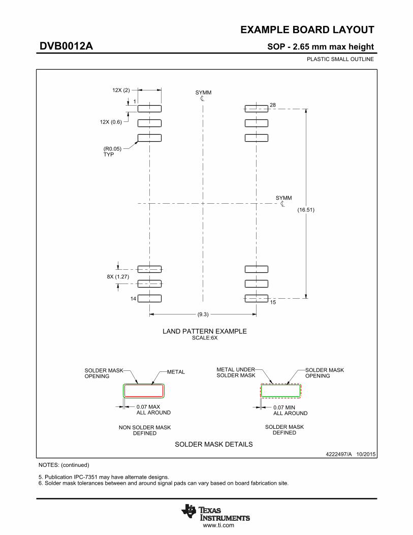
EXAMPLE BOARD LAYOUT
(9.3)
0.07 MAXALL AROUND
0.07 MINALL AROUND
12X (2)
12X (0.6)
8X (1.27)
(R )TYP
0.05
(16.51)
4222497/A 10/2015
SOP - 2.65 mm max heightDVB0012APLASTIC SMALL OUTLINE
SYMM
SYMM
LAND PATTERN EXAMPLESCALE:6X
1
1415
28
NOTES: (continued) 5. Publication IPC-7351 may have alternate designs. 6. Solder mask tolerances between and around signal pads can vary based on board fabrication site.
METALSOLDER MASKOPENING
NON SOLDER MASKDEFINED
SOLDER MASK DETAILS
SOLDER MASKOPENING
METAL UNDERSOLDER MASK
SOLDER MASKDEFINED

www.ti.com
EXAMPLE STENCIL DESIGN
(9.3)
8X (1.27)
12X (0.6)
12X (2)
(R )0.05
(16.51)
4222497/A 10/2015
SOP - 2.65 mm max heightDVB0012APLASTIC SMALL OUTLINE
NOTES: (continued) 7. Laser cutting apertures with trapezoidal walls and rounded corners may offer better paste release. IPC-7525 may have alternate design recommendations. 8. Board assembly site may have different recommendations for stencil design.
SYMM
SYMM
1
1415
28
SOLDER PASTE EXAMPLEBASED ON 0.125 mm THICK STENCIL
SCALE:6X

IMPORTANT NOTICE
Texas Instruments Incorporated (TI) reserves the right to make corrections, enhancements, improvements and other changes to itssemiconductor products and services per JESD46, latest issue, and to discontinue any product or service per JESD48, latest issue. Buyersshould obtain the latest relevant information before placing orders and should verify that such information is current and complete.TI’s published terms of sale for semiconductor products (http://www.ti.com/sc/docs/stdterms.htm) apply to the sale of packaged integratedcircuit products that TI has qualified and released to market. Additional terms may apply to the use or sale of other types of TI products andservices.Reproduction of significant portions of TI information in TI data sheets is permissible only if reproduction is without alteration and isaccompanied by all associated warranties, conditions, limitations, and notices. TI is not responsible or liable for such reproduceddocumentation. Information of third parties may be subject to additional restrictions. Resale of TI products or services with statementsdifferent from or beyond the parameters stated by TI for that product or service voids all express and any implied warranties for theassociated TI product or service and is an unfair and deceptive business practice. TI is not responsible or liable for any such statements.Buyers and others who are developing systems that incorporate TI products (collectively, “Designers”) understand and agree that Designersremain responsible for using their independent analysis, evaluation and judgment in designing their applications and that Designers havefull and exclusive responsibility to assure the safety of Designers' applications and compliance of their applications (and of all TI productsused in or for Designers’ applications) with all applicable regulations, laws and other applicable requirements. Designer represents that, withrespect to their applications, Designer has all the necessary expertise to create and implement safeguards that (1) anticipate dangerousconsequences of failures, (2) monitor failures and their consequences, and (3) lessen the likelihood of failures that might cause harm andtake appropriate actions. Designer agrees that prior to using or distributing any applications that include TI products, Designer willthoroughly test such applications and the functionality of such TI products as used in such applications.TI’s provision of technical, application or other design advice, quality characterization, reliability data or other services or information,including, but not limited to, reference designs and materials relating to evaluation modules, (collectively, “TI Resources”) are intended toassist designers who are developing applications that incorporate TI products; by downloading, accessing or using TI Resources in anyway, Designer (individually or, if Designer is acting on behalf of a company, Designer’s company) agrees to use any particular TI Resourcesolely for this purpose and subject to the terms of this Notice.TI’s provision of TI Resources does not expand or otherwise alter TI’s applicable published warranties or warranty disclaimers for TIproducts, and no additional obligations or liabilities arise from TI providing such TI Resources. TI reserves the right to make corrections,enhancements, improvements and other changes to its TI Resources. TI has not conducted any testing other than that specificallydescribed in the published documentation for a particular TI Resource.Designer is authorized to use, copy and modify any individual TI Resource only in connection with the development of applications thatinclude the TI product(s) identified in such TI Resource. NO OTHER LICENSE, EXPRESS OR IMPLIED, BY ESTOPPEL OR OTHERWISETO ANY OTHER TI INTELLECTUAL PROPERTY RIGHT, AND NO LICENSE TO ANY TECHNOLOGY OR INTELLECTUAL PROPERTYRIGHT OF TI OR ANY THIRD PARTY IS GRANTED HEREIN, including but not limited to any patent right, copyright, mask work right, orother intellectual property right relating to any combination, machine, or process in which TI products or services are used. Informationregarding or referencing third-party products or services does not constitute a license to use such products or services, or a warranty orendorsement thereof. Use of TI Resources may require a license from a third party under the patents or other intellectual property of thethird party, or a license from TI under the patents or other intellectual property of TI.TI RESOURCES ARE PROVIDED “AS IS” AND WITH ALL FAULTS. TI DISCLAIMS ALL OTHER WARRANTIES ORREPRESENTATIONS, EXPRESS OR IMPLIED, REGARDING RESOURCES OR USE THEREOF, INCLUDING BUT NOT LIMITED TOACCURACY OR COMPLETENESS, TITLE, ANY EPIDEMIC FAILURE WARRANTY AND ANY IMPLIED WARRANTIES OFMERCHANTABILITY, FITNESS FOR A PARTICULAR PURPOSE, AND NON-INFRINGEMENT OF ANY THIRD PARTY INTELLECTUALPROPERTY RIGHTS. TI SHALL NOT BE LIABLE FOR AND SHALL NOT DEFEND OR INDEMNIFY DESIGNER AGAINST ANY CLAIM,INCLUDING BUT NOT LIMITED TO ANY INFRINGEMENT CLAIM THAT RELATES TO OR IS BASED ON ANY COMBINATION OFPRODUCTS EVEN IF DESCRIBED IN TI RESOURCES OR OTHERWISE. IN NO EVENT SHALL TI BE LIABLE FOR ANY ACTUAL,DIRECT, SPECIAL, COLLATERAL, INDIRECT, PUNITIVE, INCIDENTAL, CONSEQUENTIAL OR EXEMPLARY DAMAGES INCONNECTION WITH OR ARISING OUT OF TI RESOURCES OR USE THEREOF, AND REGARDLESS OF WHETHER TI HAS BEENADVISED OF THE POSSIBILITY OF SUCH DAMAGES.Unless TI has explicitly designated an individual product as meeting the requirements of a particular industry standard (e.g., ISO/TS 16949and ISO 26262), TI is not responsible for any failure to meet such industry standard requirements.Where TI specifically promotes products as facilitating functional safety or as compliant with industry functional safety standards, suchproducts are intended to help enable customers to design and create their own applications that meet applicable functional safety standardsand requirements. Using products in an application does not by itself establish any safety features in the application. Designers mustensure compliance with safety-related requirements and standards applicable to their applications. Designer may not use any TI products inlife-critical medical equipment unless authorized officers of the parties have executed a special contract specifically governing such use.Life-critical medical equipment is medical equipment where failure of such equipment would cause serious bodily injury or death (e.g., lifesupport, pacemakers, defibrillators, heart pumps, neurostimulators, and implantables). Such equipment includes, without limitation, allmedical devices identified by the U.S. Food and Drug Administration as Class III devices and equivalent classifications outside the U.S.TI may expressly designate certain products as completing a particular qualification (e.g., Q100, Military Grade, or Enhanced Product).Designers agree that it has the necessary expertise to select the product with the appropriate qualification designation for their applicationsand that proper product selection is at Designers’ own risk. Designers are solely responsible for compliance with all legal and regulatoryrequirements in connection with such selection.Designer will fully indemnify TI and its representatives against any damages, costs, losses, and/or liabilities arising out of Designer’s non-compliance with the terms and provisions of this Notice.
Mailing Address: Texas Instruments, Post Office Box 655303, Dallas, Texas 75265Copyright © 2018, Texas Instruments Incorporated